


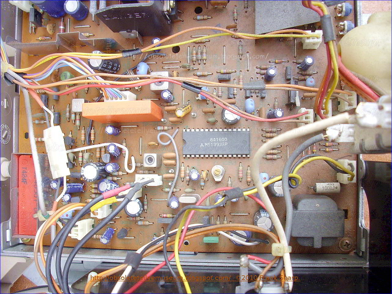
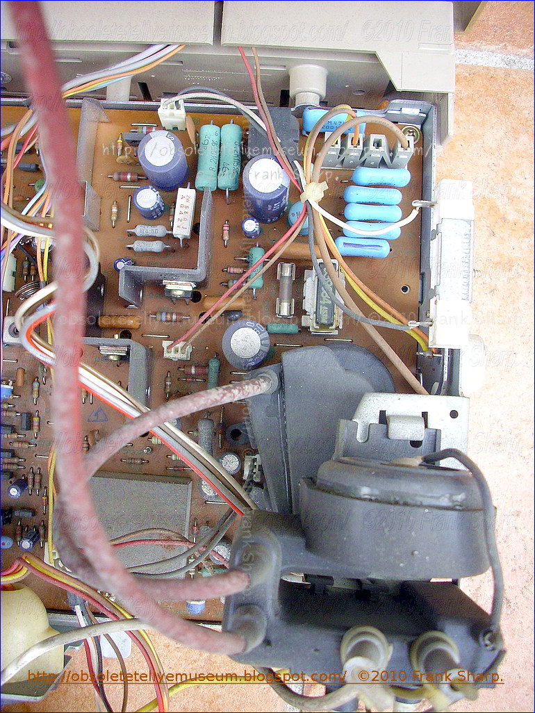


COMMODORE MODEL NO. 1701 CHASSIS GE-100A CK10151-B01 CK30170-B01 CK30169-B01 PAL system color.
B1 VOLTAGE - inject a video signal
1701 (11OV)
Regulate VR, R109, for B, adjustment so that DC voltage between TP-91 and earth is 110 volts.
1702 (125V.)
Confirm that the voltage at TP-94 and IC901 pin 4 is 125 volts.
NOTE: Meter should be periodically calibrated at 20K ohms/volt.
FOCUS
Adjust the FOCUS control for best overall definition and picture detail at normal brightness and contrast.
VERTICAL POSITION
Adjust the V. center VR R428 (R429) to the optimum vertical picture position.
VERTICAL HEIGHT AND LINEARITY
1. Display a pattern which allows easy
confirmation of symmetry (such as a circle or crosshatch).
2. Reduce the vertical size with the V.
HEIGHT VR.
3. Adjust the vertical linearity with the
V. LIN. VR.
4. Readjust the vertical height, so that
the picture extends to normal size.
HORIZONTAL WIDTH
Adjust H. WIDTH control coil L503 (L522) by turning it with a hexagonal adjusting bar only if RIGHT
and LEFT sides of picture can’t be seen.
HORIZONTAL OSCILLATOR
1. Set the H. FREQ. VR to the mechanical center position.
2. Connect a jumper clip between TP-33A and TP-33B.
3. While rotating the H. FREQ. VR, R504, keep the picture stationary or slowly moving.
4. Remove the jumper wire.
5. Make sure that the set maintains horizontal sync, when signals are switched.
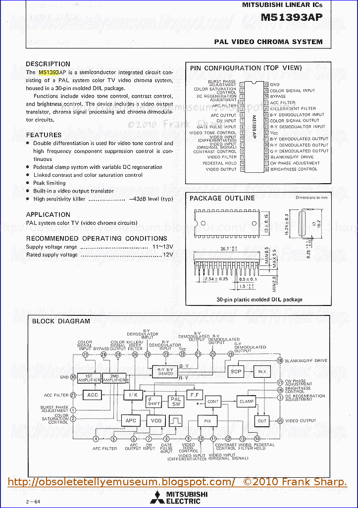
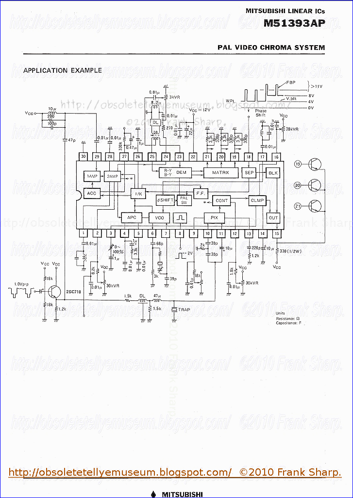
M51393AP PAL VIDEO CHROMA SYSTEM:
DESCR IPTION
The M51393AP is a semiconductor integrated circuit con'sisting of a PAL system color TV video chroma system,
housed in a 30-pin molded DIL package
Functions include video tone control, contrast control,
and brightness control. The device includes a video output
transistor, chroma signal processing and chroma demodulator circuits.
FEATURES
• Double differentiation 'is used for video tone control and
high frequency component suppression control is continuous
• Pedestal clamp system with variable DC regeneration
• Linked contrast and color saturation control
• Peak limiting
'*. Built-in a video output transistor
• High sensitivity killer
-43dB level (typ)
APPLICATION PAL system color TV (video chroma circuits)
Power supply is realized with mains transformer
and Linear transistorized power supply stabilizer, A DC power supply
apparatus includes a rectifier circuit which rectifies an input
commercial AC voltage. The rectifier output voltage is smoothed in a
smoothing capacitor. Voltage stabilization is provided in the
stabilizing circuits by the use of Zener diode circuits to provide
biasing to control the collector-emitter paths of respective
transistors.A linear regulator circuit according to an embodiment of
the present invention has an input node receiving an unregulated
voltage and an output node providing a regulated voltage. The linear
regulator circuit includes a voltage regulator, a bias circuit, and a
current control device.
In one embodiment, the current
control device is implemented as an NPN bipolar junction transistor
(BJT) having a collector electrode forming the input node of the linear
regulator circuit, an emitter electrode coupled to the input of the
voltage regulator, and a base electrode coupled to the second terminal
of the bias circuit. A first capacitor may be coupled between the input
and reference terminals of the voltage regulator and a second
capacitor may be coupled between the output and reference terminals of
the voltage regulator. The voltage regulator may be implemented as
known to those skilled in the art, such as an LDO or non-LDO 3-terminal
regulator or the like.
In the bias device and current source embodiment, the bias device may be implemented as a Zener diode, one or more diodes coupled in series, at least one light emitting diode, or any other bias device which develops sufficient voltage while receiving current from the current source. The current source may be implemented with a PNP BJT having its collector electrode coupled to the second terminal of the bias device, at least one first resistor having a first end coupled to the emitter electrode of the PNP BJT and a second end, a Zener diode and a second resistor. The Zener diode has an anode coupled to the base electrode of the PNP BJT and a cathode coupled to the second end of the first resistor. The second resistor has a first end coupled to the anode of the Zener diode and a second end coupled to the reference terminal of the voltage regulator. A second Zener diode may be included having an anode coupled to the cathode of the first Zener diode and a cathode coupled to the first current electrode of the current control device.
A circuit is disclosed for improving operation of a linear regulator, having an input terminal, an output terminal, and a reference terminal. The circuit includes an input node, a transistor, a bias circuit, and first and second capacitors. The transistor has a first current electrode coupled to the input node, a second current electrode for coupling to the input terminal of the linear regulator, and a control electrode. The bias circuit has a first terminal for coupling to the output terminal of the linear regulator and a second terminal coupled to the control electrode of the transistor. The first capacitor is for coupling between the input and reference terminals of the linear regulator, and the second capacitor is for coupling between the output and reference terminals of the linear regulator. The bias circuit develops a voltage sufficient to drive the control terminal of the transistor and to operate the linear regulator. The bias circuit may be a battery, a bias device and a current source, a floating power supply, a charge pump, or any combination thereof. The transistor may be implemented as a BJT or FET or any other suitable current controlled device.

Power Supply: The examples chosen are taken from manufacturers' circuit diagrams and are usually simplified to emphasise the fundamental nature of the circuit. For each example the particular transistor properties that are exploited to achieve the desired performance are made clear. As a rough and ready classification the circuits are arranged in order of frequency: this part is devoted to circuits used at zero frequency, field frequency and audio frequencies. Series Regulator Circuit Portable television receivers are designed to operate from batteries (usually 12V car batteries) and from the a.c. mains. The receiver usually has an 11V supply line, and circuitry is required to ensure that the supply line is at this voltage whether the power source is a battery or the mains. The supply line also needs to have good regulation, i.e. a low output resistance, to ensure that the voltage remains constant in spite of variations in the mean current taken by some of the stages in the receiver. Fig. 1 shows a typical circuit of the power -supply arrangements. The mains transformer and bridge rectifier are designed to deliver about 16V. The battery can be assumed to give just over 12V. Both feed the regulator circuit Trl, Tr2, Tr3, which gives an 11V output and can be regarded as a three -stage direct -coupled amplifier. The first stage Tr 1 is required to give an output current proportional to the difference between two voltages, one being a constant voltage derived from the voltage reference diode D I (which is biased via R3 from the stabilised supply).

The second voltage is obtained from a preset potential divider connected across the output of the unit, and is therefore a sample of the output voltage. In effect therefore Tr 1 compares the output voltage of the unit with a fixed voltage and gives an output current proportional to the difference between them. Clearly a field-effect transistor could do this, but the low input resistance of a bipolar transistor is no disadvantage and it can give a current output many times that of a field-effect transistor and is generally preferred therefore. The output current of the first stage is amplified by the two subsequent stages and then becomes the output current of the unit. Clearly therefore Tr2 and Tr3 should be current amplifiers and they normally take the form of emitter followers or common emitter stages (which have the same current gain). By adjusting the preset control we can alter the fraction of the output voltage' applied to the first stage and can thus set the output voltage of the unit at any desired value within a certain range. By making assumptions about the current gain of the transistors we can calculate the degree of regulation obtainable. For example, suppose the gain of Tr2 and Tr3 in cascade is 1,000, and that the current output demanded from the unit changes by 0.1A (for example due to the disconnection of part of the load). The corresponding change in Tr l's collector current is 0.1mA and, if the standing collector current of Tr 1 is 1mA, then its mutual conductance is approximately 4OmA/V and the base voltage must change by 2.5mV to bring about the required change in collector current. If the preset potential divider feeds one half of the output voltage to Tr l's base, then the change in output voltage must be 5mV. Thus an 0.1A change in output current brings about only 5mV change in output voltage: this represents an output resistance of only 0.0552.
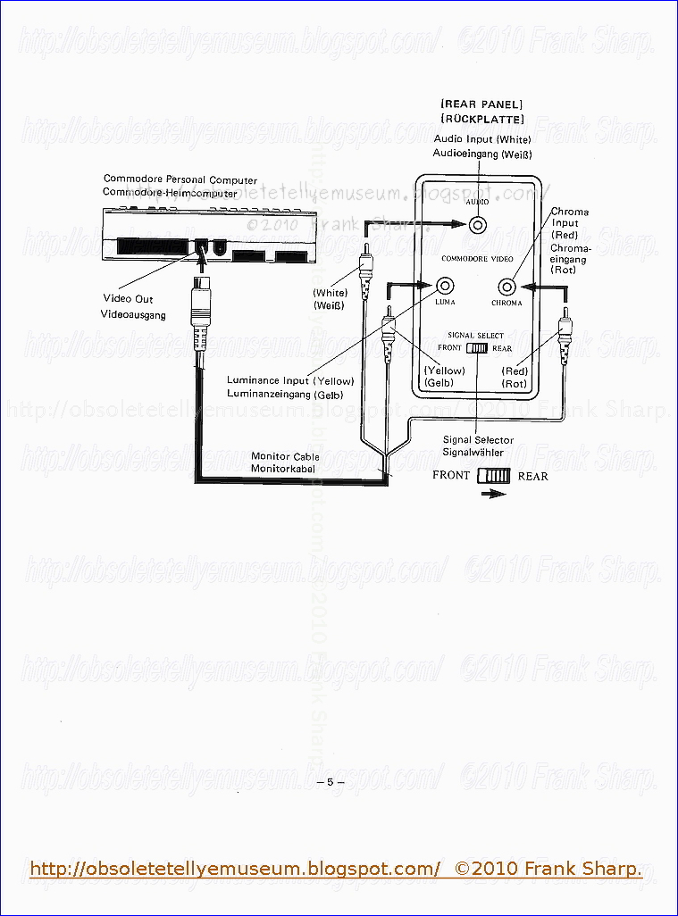
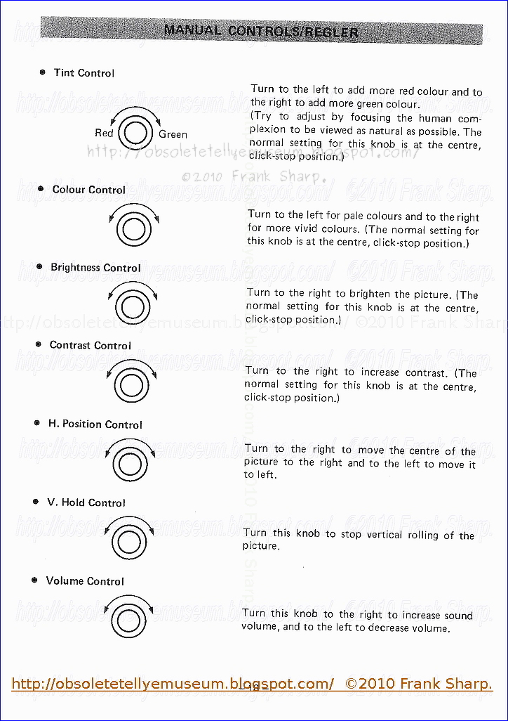
COMMODORE MODEL NO. 1701 CHASSIS GE-100A USER MANUAL PAGES:


No comments:
Post a Comment
The most important thing to remember about the Comment Rules is this:
The determination of whether any comment is in compliance is at the sole discretion of this blog’s owner.
Comments on this blog may be blocked or deleted at any time.
Fair people are getting fair reply. Spam and useless crap and filthy comments / scrapers / observations goes all directly to My Private HELL without even appearing in public !!!
The fact that a comment is permitted in no way constitutes an endorsement of any view expressed, fact alleged, or link provided in that comment by the administrator of this site.
This means that there may be a delay between the submission and the eventual appearance of your comment.
Requiring blog comments to obey well-defined rules does not infringe on the free speech of commenters.
Resisting the tide of post-modernity may be difficult, but I will attempt it anyway.
Your choice.........Live or DIE.
That indeed is where your liberty lies.
Note: Only a member of this blog may post a comment.