


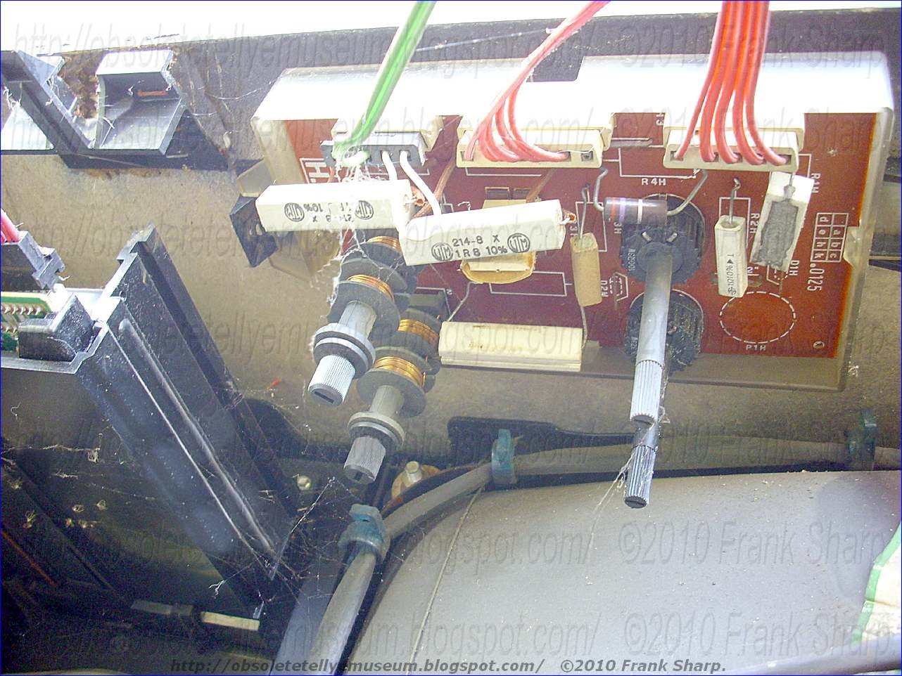


Power Supply Unit (Dual Power Thyristor with PHILIPS BR161 phase regulated !)
AUTOVOX TVC2278 ALTAIR CHASSIS 100 POWER
Supply CONSTANT-VOLTAGE CONVERTER EMPLOYING THYRISTOR:

A constant voltage converter having a rectifier for rectifying AC power and with a thyristor connected between the rectifier and a filter for selectively passing therethrough a rectified output to an output terminal. There is a wave generator connected to the output of the rectifier for producing a first signal and an intergrator circuit connected to the output of the wave generator for producing an integral output in response to this first signal. In addition there is a detector circuit for detecting a fluctuation of the rectified output power and for producing second signal. A comparison circuit is connected between the intergrator circuit and the detector circuit for producing third signal in accordance with the comparison. A trigger circuit is connected between the comparison circuit and the control gate of the thyristor for supplying a phase control signal to the thyristor to thereby obtain a constant voltage output regardless of the fluctuation of the rectified output.
AUTOVOX TVC2278 ALTAIR CHASSIS 100 POWER
Supply CONSTANT-VOLTAGE CONVERTER EMPLOYING THYRISTOR:
A constant voltage converter having a rectifier for rectifying AC power and with a thyristor connected between the rectifier and a filter for selectively passing therethrough a rectified output to an output terminal. There is a wave generator connected to the output of the rectifier for producing a first signal and an intergrator circuit connected to the output of the wave generator for producing an integral output in response to this first signal. In addition there is a detector circuit for detecting a fluctuation of the rectified output power and for producing second signal. A comparison circuit is connected between the intergrator circuit and the detector circuit for producing third signal in accordance with the comparison. A trigger circuit is connected between the comparison circuit and the control gate of the thyristor for supplying a phase control signal to the thyristor to thereby obtain a constant voltage output regardless of the fluctuation of the rectified output.

1. A constant voltage converter comprising an input of a power supply means, an output terminal, filter means, rectifier means connected to said input for rectifying a.c. power and for supplying output thereof to said output terminal, thyristor means connected between said rectifier means and said filter means for selectively passing therethrough a rectified output to the output terminal by way of said filter means, saw-tooth wave generator means connected between the output of said rectifier means and at least one integrator circuit means for producing an integral output in response to a saw-tooth wave produced, a first transistor in said saw-tooth wave generator, the input of said integrator circuit means being connected to a collector of said first transistor, detector circuit means connected to said output terminal for detecting a fluctuation of the rectified output power and for producing an output signal, said detector circuit me
ans having a second transistor, pulse generator circuit means connected between said saw-tooth wave generator means and said detector circuit means for producing a trigger pulse to said thyristor through a trigger means, a third transistor in said pulse circuit generator means, the base of said third transistor being connected to the output of said integrator circuit means, the emitter thereof being connected to the emitter of said second transistor in said detector circuit means, and the collector thereof being connected to the gate of the thyristor means so as to supply a phase control signal thereto, thereby obtaining a constant voltage output regardless of the fluctuation of the rectified output.
Description:
This invention relates to constant-voltage converters and more particularly to a constant-voltage converter employing a thyristor.
Conventional constant-voltage converters of the type employing a thyristor are arranged to phase shift and full-wave-rectify an input a.c. power applied thereto and to maintain the output voltages constant by regulating the firing angle of the thyristor in comparison of the output voltages with the phase-shifted and rectified input a.c. power. When, however, these converters are connected to a common a.c. source having a relatively high internal impedance, the waveform of the phase-shifted and rectified a.c. input power is distorted thereby causing undesired operations of the converters.
It is therefore an object of the present invention to provide a constant-voltage converter which correctly operates notwithstanding the distortion of the input a.c. voltage.
Another object of the invention is to provide a constant-voltage converter which effectively suppress an undesired rush current.
Another object of the invention is to provide a constant-voltage converter having an improved feed-back circuit of a substantially constant loop gain .
In the drawings:
FIG. 1 is a schematic view of a converter according to the present invention;
FIG. 2 is a diagram showing a circuit arrangement of the converter of FIG. 1;
FIG. 3 is a diagram showing various waveforms of signals appearing in the circuit of FIG. 2;
FIG. 4 is a diagram showing various waveforms appearing in the circuit of FIG. 2 when an a.c. power is supplied to the circuit;
FIG. 5 is a diagram showing another circuit arrangement of the converter of FIG. 1;
FIG. 6 is a diagram showing waveforms of signals appearing in the circuit of FIG. 5; and
FIG. 7 is a diagram showing further another circuit arrangement of generator the of FIG. 1.
Referring now to FIG. 1, a cons tant-voltage converter 10 according to the present invention comprises a rectifier 11 having two input terminals 12 and 13 through which an a.c. power is supplied. The rectifier 11 is preferably a full-wave rectifier although a half-wave rectifier may be employed. An output 14 of the rectifier 11 is connected through a line 15 to an anode of a thyristor 16. The thyristor 16 passes therethrough the rectified a.c. power in only one direction from its anode to cathode when triggered by a trigger pulse through its gate. The cathode of the thyristor 16 is connected through a line 17 to an input of a smoothing filter 18. The smoothing filter 18 smoothes the power from the thyristor 16. An output of the smoothing filter 18 is connected through a line 19 to an output terminal 20. The output 14 of the rectifier 11 is also connected through a line 21 to a saw-tooth wave generator 22 which generates a saw-tooth wave signal having the same repetition period as the rectified input a.c. power. An output of the saw-tooth wave generator 22 is connected through a line 23 to one input of a trigger pulse generator 24. The other input of the trigger pulse generator 24 is connected through a line 25 to the line 19. An output of the trigger pulse generator 24 is connected through a line 26 to the gate of the thyristor 16. The trigger pulse generator 24 produces a trigger pulse on its output when the voltage of the saw-tooth wave signal reaches a level which is varied in response to the output voltage on the terminal 20. The trigger pulse generator 24 may be variously arranged and in this case arranged to comprise rectangular generator 27 having one input connected through the line 23 to the saw-tooth wave generator 22 and the other input connected through a line 28 to an output voltage detector 29. The detector 29 produces a reference signal representing the output voltage on the terminal 20. The pulse generator 27 is adapted to produces a rectangular pulse when the saw-tooth wave signal to the one input reaches a level which defined is in accordance with the reference signal. An output of the rectangular pulse generator 27 is connected through a line 30 to an input of a trigger circuit 31. The trigger circuit 31 is adapted to convert the rectangular pulse into a spike pulse. An output of the trigger circuit 31 is connected through the line 26 to the gate of the thyristor 16.
FIG. 2 illustrates a prefe rred circuit arrangement of the converter shown in FIG. 1 which comprises a rectifier 11 of a full-wave rectifier consisting of rectifiers 40, 41, 42 and 43. Inputs of the rectifier are connected to terminals 12 and 13 through which an a.c. power is applied. The output 14 of the rectifier 11 is connected through a line 15 to an anode of a thyristor 16. A cathode of the thyristor 16 is connected through a line 17 to a smoothing filter 18 which includes a capacitor C4 having one terminal connected to the line 17 and the other terminal grounded. The output of the smoothing filter 18 is connected through a line 19 to an output terminal 20.
The saw-tooth wave generator 22 includes a resistor R 1 having one terminal connected to the line 21 and the terminal connected through a junction J 1 to one terminal of a resistor R 2 . The other terminal of the resistor R 2 is grounded. The junction J 1 is connected through a coupling capacitor C 1 to a base of a transistor T 1 of PNP type. An emitter of the transistor T 1 is connected through a resistor R 3 to the line 21. A resistor R 4 is provided between the emitter and the base of the transistor T 1 so as to apply a bias potential to the base. A collector of the transistor T 1 is grounded th rough a parallel connection of a resistor R 5 and capacitor C 2 . To the emitter is connected a capacitor C 3 which is in turn grounded and passes therethrough only a.c. signals to the ground.
The rectangular pulse generator 27 comprises a transistor T 2 of PNP type having a base connected through a resistor R 6 to the collector of the transistor T 1 . An emitter of the transistor T 2 is connected through a resistor R 7 to the emitter of the transistor T 1 . A collector of the transistor T 2 is grounded through a resistor R 8 and connected through the line 30 to one terminal of a capacitor C 4 of the trigger circuit 31. The other terminal of the capacitor C 4 is connected through a line 26 to the gate of the thyristor 16.
The output voltage detector 29 includes a transistor T 3 of NPN type having an emitter grounded through a zener diode ZD. A collector of the transistor T 3 is connected through a line 28 to the emitter of the transistor T 2 and, on the other hand, connected through a capacitor C 5 to the grounded. A base of the transistor T 3 is connected to a tap of an adjustable resistor R 9 connected through a resistor R 10 and a line 25 to the line 19 and connected, in turn, to the ground through a resistor R 11 .
When, in operation, an a.c. electric power is applied through the input terminals 12 and 13 of the rectif ier 11, a full-wave rectified power as shown in FIG. 3 (a) appears on the output 14. The rectified power is applied through the line 15 to the anode of the thyristor 16. The thyristor 16 passes therethrough the rectified power while its firing angle is regulated by the trigger signal applied to the gate. The rectified power passed through the thyristor 16 is applied through the line 17 to the smoothing filter 18. The smoothing filter smoothes the power by removing the ripple component in the power. The smoothed power appears on the line 19 which is to be supplied to a load through the output terminal 20. The smoothed power on the line 19 is, on the other hand, delivered through the line 25 to the resistor R 10 of the output voltage detector 29. The resistor R 10 constitutes a voltage divider in cooperation with the resistors R 9 and R 11 . The output of the voltage divider is applied through the tap of the resistor R 9 to the base of the transistor T 3 . When the potential of the base of the transistor T 3 exceeds the zener voltage of the zener diode ZD, a base current flows through the transistor T 3 so as to render the transistor T 3 conductive. The potential of the collector of the transistor T 3 then varies in accordance with the voltage of the smoothed output power on the line 19. The potential variation at the collector of the transistor T 3 is then applied through the line 28 to the trigger pulse generator 27 and utilized to regulate the triggering timing of the thyristor 16.
The full-wave rectified power is, on the other hand, applied through the line 21 to the saw-tooth wave generator 22. Since the resistors R 1 and R 2 consistute a voltage divider to reduce the voltage of the full-wave rectified power to a potential at the junction J 1 , a charging current to the capacitor C 1 flows from the emitter to the base of the transistor T 1 whereby the transistor T 1 repeats ON-OFF operation in accordance with the voltage of the rectified power. If the transistor T 1 is conductive when the voltage of the full-wave rectified power is lower than a threshold voltage v 1 as shown in FIG. 3(a), then the potential at the collector of the transistor T 1 is varied as shown in FIG. 3 (b) due to the charge and discharge of the capacitor C 2 . The variation of the potential at the collector of the transistor T 1 is supplied through the line 23 to the resistor R 6 of the trigger pulse generator 27.
As long as the voltage of the smoothed power on the line 19 equals to the rated output voltage, the transistor T 2 is adapted to become conductive when the voltage of the saw-tooth wave signal falls below a threshold value v 3 shown in FIG. 3(b). Therefore, a potential at the collector of the transistor T 2 varies as shown in FIG. 3(c). The potential variation, that is, a pulse signal at the collector of the transistor T 2 is supplied through the line 30 to the capacitor C 4 of the trigger circuit trigger 31. The trigger circuit 31 converts the pulse signal into a spike pulse or a trigger pulse shown in FIG. 3(d) which is then applied through the line 25 to the gate of the thyristor 16. Upon receiving the spike pulse, the thyristor 16 becomes conductive until the voltage of the rectified power on the line 15 falls below the cut-off voltage of the thyristor 16.
When the voltage of the smoothed power on the line 19 exceeds the rated output voltage, the collector current of the transistor T 3 increases with the result that the current flowing through the resistor R 7 increases. The threshold voltage of the transistor T 2 therefore reduces to a voltage v 2 as shown in FIG. 3(b). At this instant, leading edge of the pulse signal delays as shown by dot-and-dash lines in FIG. 3(c), so that each trigger pulse delays as shown by dot-and-dash line in FIG. 3(d). When on the contrary, the voltage of the smoothed signal on the line 19 lowers below the rated output voltage, the collector current of the transistor T 3 decreases whereby the threshold voltage rises to a voltage v 4 in FIG. 3(b). Each leading edge of the signal pulse now leads as shown by dotted line in FIG. 3(d). Being apparent from the above description, the appearance timing of each trigger pulse is regulated in accordance with the voltage of the smoothed power on the line 19 so that the voltage of the output voltage at the terminal 20 is held substantially constant.
Referring now to FIG. 4, start operation of the converte r 10 is discussed hereinbelow in conjunction with FIG. 2. When an a.c. voltage is applied to the input terminals 12 and 13, the capacitor C 3 begins to be charged by the voltage on the line 15, and the capacitor C 5 also begins to be charged through the resistors R 3 and R 7 . It is important that the time constant of power supply circuit constituted by the resistor R 3 and the capacitor C 3 is selected to be much larger than that of the time constant of another power supply circuit constituted by the resistor R 7 and the capacitor C 5 . Thus, the emitter potential of the transistor T 1 is built up more quickly than that of the transistor T 2 . Upon completion of the charging of the capacitor C 3 , the saw-tooth wave generator 22 begins to generate saw-tooth wave signal as shown in FIG. 4(b). Since the capacitor C 5 is, on the other hand, slowly charged, the emitter voltage of the transistor T 2 slowly rises as shown in FIG. 4(c), so that, the threshold voltage of the transistor T 2 gradually rises as shown by a dotted line in FIG. 4 (b). Accordingly, the trigger pulses is produced on the gate of the thyristor 16 as shown in FIG. 4(d), whereby the firing angle of the thyristor 16 is gradually reduced as shown in FIG. 4(a) which illustrates the voltage at the output terminal 14 of the rectifier 11. The output voltage on the output terminal 20 therefore gradually rise up as shown in FIG. 4(e). It is to be understood that since the output voltage of the converter 10 starts to gradually rise up as shown in FIG. 4(e), an undesired rush current is effectively suppressed.
FIG. 5 illustrates another fo rm of the converter 10 which is arranged identically to the circuit arrangement of FIG. 1 except that an integrator 50 is interposed between the output of the saw-tooth wave generator 22 and the input of the trigger pulse generator 27. The integrator 50 includes a resistor R 12 having one terminal connected to the output of the saw-tooth wave generator 22 and the other terminal connected to the input of the rectangular pulse generator 27, and a capacitor C 7 having one terminal connected to the other terminal of the resistor R 12 and the other terminal grounded.
In operation, the saw-tooth wave generator 22 produces on its ouput a saw-tooth wave signal having decreasing exponential wave form portion as shown in FIG. 6 (a), although the saw-tooth wave signal ideally is illustrated in FIG. 3. This saw-tooth wave signal is converted by the integrator 50 into another form of saw-tooth wave having a increasing exponential wave form portion as shown in FIG. 6(b).
It should be noted that the saw-tooth wave signal of FIG. 6(a) has a smaller inclination near 180°. Hence, when the integrator 50 is omitted and the saw-tooth wave signal as shown in FIG. 6(a) is applied to the trigger pulse generator 27, the rate of change of the output voltage of the converter 10 become larger at a firing angle near to 1 80°. On the other hand, it is apparent from FIG. 6(c) that the rate of change the output voltage of the thyristor 16 with respect to the firing angle become large at a firing angle near to 180°. Therefore, the loop gain of the trigger pulse generator 24 increases when the firing angle of the thyristor 16 is near to 180°. It is apparent through a similar discussion that the loop gain of the trigger pulse generator 24 decreases when the firing angle is near to 90°. Such non-uniformity of the loop gain of the trigger pulse generator invites a difficulty of the regulation of the output voltage of the converter. It is to be noted that the saw-tooth wave signal shown in FIG. 6(b) has a large inclination at an angle near 180°. Therefore, when the saw-tooth wave signal of FIG. 6(b) is applied to the trigger pulse generator 24, the loop gain of the trigger pulse generator 24 is held substantially constant, whereby the output voltage of the converter is effectively held constant.
 It is to be understood that the integrator 50 may be substituted for by a miller integrator and a bootstrap integrator. Furthermore, a plurality of integrator may be employed, if desired.
FIG. 7 illustrates another circuit arrangement of the converter according to the present invention, which is arranged identically to the circuit of FIG. 2 except for the trigger circuit 31 and the smoothing circuit 18.
The trigger circuit 31 of FIG. 7 comprises a transformer TR with primary and secondary coils. One terminal of the primary coil is connected to the resistor R 7 of the pulse generator 27. The other terminal of the primary coil is connected to a collector of a transistor T 4 of NPN type. The secondary coil has terminals respectively con nected to the gate and cathode of the thyristor 16. An emitter of the transistor T 4 is grounded through a resistor R 13 . A base of the transistor T 4 is grounded through a resistor R 14 and connected through a capacitor C 8 to the collector of the transistor T 2 of the pulse generator 27.
The smoothing filter 18 of FIG. 7 comprises a choke coil CH connected to the lines 17 and 19, and to capacitors C 9 and C 10 which are in turn grounded. The circuit of FIG. 7 operates in the same manner as the circuit of FIG. 2.
Obviously many modifications and variations of the present invention are possible in the light of the above teachings. It is therefore to be understood that within the scope of the appended claims the invention may be practiced otherwise than as specifically described.
Conventional constant-voltage converters of the type employing a thyristor are arranged to phase shift and full-wave-rectify an input a.c. power applied thereto and to maintain the output voltages constant by regulating the firing angle of the thyristor in comparison of the output voltages with the phase-shifted and rectified input a.c. power. When, however, these converters are
connected to a common a.c. source having a relatively high internal impedance, the waveform of the phase-shifted and rectified a.c. input power is distorted thereby causing undesired operations of the converters.It is therefore an object of the present invention to provide a constant-voltage converter which correctly operates notwithstanding the distortion of the input a.c. voltage.
Another object of the invention is to provide a constant-voltage converter which effectively suppress an undesired rush current.
Another object of the invention is to provide a constant-voltage converter having an improved feed-back circuit of a substantially constant loop gain .
In the drawings:
FIG. 1 is a schematic view of a converter according to the present invention;
FIG. 2 is a diagram showing a circuit arrangement of the converter of FIG. 1;
FIG. 3 is a diagram showing various waveforms of signals appearing in the circuit of FIG. 2;
FIG. 4 is a diagram showing various waveforms appearing in the circuit of FIG. 2 when an a.c. power is supplied to the circuit;
FIG. 5 is a diagram showing another circuit arrangement of the converter of FIG. 1;
FIG. 6 is a diagram showing waveforms of signals appearing in the circuit of FIG. 5; and
FIG. 7 is a diagram showing further another circuit arrangement of generator the of FIG. 1.
Referring now to FIG. 1, a cons
tant-voltage converter 10 according to the present invention comprises a rectifier 11 having two input terminals 12 and 13 through which an a.c. power is supplied. The rectifier 11 is preferably a full-wave rectifier although a half-wave rectifier may be employed. An output 14 of the rectifier 11 is connected through a line 15 to an anode of a thyristor 16. The thyristor 16 passes therethrough the rectified a.c. power in only one direction from its anode to cathode when triggered by a trigger pulse through its gate. The cathode of the thyristor 16 is connected through a line 17 to an input of a smoothing filter 18. The smoothing filter 18 smoothes the power from the thyristor 16. An output of the smoothing filter 18 is connected through a line 19 to an output terminal 20. The output 14 of the rectifier 11 is also connected through a line 21 to a saw-tooth wave generator 22 which generates a saw-tooth wave signal having the same repetition period as the rectified input a.c. power. An output of the saw-tooth wave generator 22 is connected through a line 23 to one input of a trigger pulse generator 24. The other input of the trigger pulse generator 24 is connected through a line 25 to the line 19. An output of the trigger pulse generator 24 is connected through a line 26 to the gate of the thyristor 16. The trigger pulse generator 24 produces a trigger pulse on its output when the voltage of the saw-tooth wave signal reaches a level which is varied in response to the output voltage on the terminal 20. The trigger pulse generator 24 may be variously arranged and in this case arranged to comprise rectangular generator 27 having one input connected through the line 23 to the saw-tooth wave generator 22 and the other input connected through a line 28 to an output voltage detector 29. The detector 29 produces a reference signal representing the output voltage on the terminal 20. The pulse generator 27 is adapted to produces a rectangular pulse when the saw-tooth wave signal to the one input reaches a level which defined is in accordance with the reference signal. An output of the rectangular pulse generator 27 is connected through a line 30 to an input of a trigger circuit 31. The trigger circuit 31 is adapted to convert the rectangular pulse into a spike pulse. An output of the trigger circuit 31 is connected through the line 26 to the gate of the thyristor 16.FIG. 2 illustrates a prefe
rred circuit arrangement of the converter shown in FIG. 1 which comprises a rectifier 11 of a full-wave rectifier consisting of rectifiers 40, 41, 42 and 43. Inputs of the rectifier are connected to terminals 12 and 13 through which an a.c. power is applied. The output 14 of the rectifier 11 is connected through a line 15 to an anode of a thyristor 16. A cathode of the thyristor 16 is connected through a line 17 to a smoothing filter 18 which includes a capacitor C4 having one terminal connected to the line 17 and the other terminal grounded. The output of the smoothing filter 18 is connected through a line 19 to an output terminal 20.The saw-tooth wave generator 22 includes a resistor R 1 having one terminal connected to the line 21 and the terminal connected through a junction J 1 to one terminal of a resistor R 2 . The other terminal of the resistor R 2 is grounded. The junction J 1 is connected through a coupling capacitor C 1 to a base of a transistor T 1 of PNP type. An emitter of the transistor T 1 is connected through a resistor R 3 to the line 21. A resistor R 4 is provided between the emitter and the base of the transistor T 1 so as to apply a bias potential to the base. A collector of the transistor T 1 is grounded th
rough a parallel connection of a resistor R 5 and capacitor C 2 . To the emitter is connected a capacitor C 3 which is in turn grounded and passes therethrough only a.c. signals to the ground.The rectangular pulse generator 27 comprises a transistor T 2 of PNP type having a base connected through a resistor R 6 to the collector of the transistor T 1 . An emitter of the transistor T 2 is connected through a resistor R 7 to the emitter of the transistor T 1 . A collector of the transistor T 2 is grounded through a resistor R 8 and connected through the line 30 to one terminal of a capacitor C 4 of the trigger circuit 31. The other terminal of the capacitor C 4 is connected through a line 26 to the gate of the thyristor 16.
The output voltage detector 29 includes a transistor T 3 of NPN type having an emitter grounded through a zener diode ZD. A collector of the transistor T 3 is connected through a line 28 to the emitter of the transistor T 2 and, on the other hand, connected through a capacitor C 5 to the grounded. A base of the transistor T 3 is connected to a tap of an adjustable resistor R 9 connected through a resistor R 10 and a line 25 to the line 19 and connected, in turn, to the ground through a resistor R 11 .
When, in operation, an a.c. electric power is applied through the input terminals 12 and 13 of the rectif
ier 11, a full-wave rectified power as shown in FIG. 3 (a) appears on the output 14. The rectified power is applied through the line 15 to the anode of the thyristor 16. The thyristor 16 passes therethrough the rectified power while its firing angle is regulated by the trigger signal applied to the gate. The rectified power passed through the thyristor 16 is applied through the line 17 to the smoothing filter 18. The smoothing filter smoothes the power by removing the ripple component in the power. The smoothed power appears on the line 19 which is to be supplied to a load through the output terminal 20. The smoothed power on the line 19 is, on the other hand, delivered through the line 25 to the resistor R 10 of the output voltage detector 29. The resistor R 10 constitutes a voltage divider in cooperation with the resistors R 9 and R 11 . The output of the voltage divider is applied through the tap of the resistor R 9 to the base of the transistor T 3 . When the potential of the base of the transistor T 3 exceeds the zener voltage of the zener diode ZD, a base current flows through the transistor T 3 so as to render the transistor T 3 conductive. The potential of the collector of the transistor T 3 then varies in accordance with the voltage of the smoothed output power on the line 19. The potential variation at the collector of the transistor T 3 is then applied through the line 28 to the trigger pulse generator 27 and utilized to regulate the triggering timing of the thyristor 16.The full-wave rectified power is, on the other hand, applied through the line 21 to the saw-tooth wave generator 22. Since the resistors R 1 and R 2 consistute a voltage divider to reduce the voltage of the full-wave rectified power to a potential at the junction J 1 , a charging current to the capacitor C 1 flows from the emitter to the base of the transistor T 1 whereby the transistor T 1 repeats ON-OFF operation in accordance with the voltage of the rectified power. If the transistor T 1 is conductive when the voltage of the full-wave rectified power is lower than a threshold voltage v 1 as shown in FIG. 3(a), then the potential at the collector of the transistor T 1 is varied as shown in FIG. 3 (b) due to the charge and discharge of the capacitor C 2 . The variation of the potential at the collector of the transistor T 1 is supplied through the line 23 to the resistor R 6 of the trigger pulse generator 27.
As long as the voltage of the smoothed power on the line 19 equals to the rated output voltage, the transistor T 2 is adapted to become conductive when the voltage of the saw-tooth wave signal falls below a threshold value v 3 shown in FIG. 3(b). Therefore, a potential at the collector of the transistor T 2 varies as shown in FIG. 3(c). The potential variation, that is, a pulse signal at the collector of the transistor T 2 is supplied through the line 30 to the capacitor C 4 of the trigger circuit trigger 31. The trigger circuit 31 converts the pulse signal into a spike pulse or a trigger pulse shown in FIG. 3(d) which is then applied through the line 25 to the gate of the thyristor 16. Upon receiving the spike pulse, the thyristor 16 becomes conductive until the voltage of the rectified power on the line 15 falls below the cut-off voltage of the thyristor 16.
When the voltage of the smoothed power on the line 19 exceeds the rated output voltage, the collector current of the transistor T 3 increases with the result that the current flowing through the resistor R 7 increases. The threshold voltage of the transistor T 2 therefore reduces to a voltage v 2 as shown in FIG. 3(b). At this instant, leading edge of the pulse signal delays as shown by dot-and-dash lines in FIG. 3(c), so that each trigger pulse delays as shown by dot-and-dash line in FIG. 3(d). When on the contrary, the voltage of the smoothed signal on the line 19 lowers below the rated output voltage, the collector current of the transistor T 3 decreases whereby the threshold voltage rises to a voltage v 4 in FIG. 3(b). Each leading edge of the signal pulse now leads as shown by dotted line in FIG. 3(d). Being apparent from the above description, the appearance timing of each trigger pulse is regulated in accordance with the voltage of the smoothed power on the line 19 so that the voltage of the output voltage at the terminal 20 is held substantially constant.
Referring now to FIG. 4, start operation of the converte
r 10 is discussed hereinbelow in conjunction with FIG. 2. When an a.c. voltage is applied to the input terminals 12 and 13, the capacitor C 3 begins to be charged by the voltage on the line 15, and the capacitor C 5 also begins to be charged through the resistors R 3 and R 7 . It is important that the time constant of power supply circuit constituted by the resistor R 3 and the capacitor C 3 is selected to be much larger than that of the time constant of another power supply circuit constituted by the resistor R 7 and the capacitor C 5 . Thus, the emitter potential of the transistor T 1 is built up more quickly than that of the transistor T 2 . Upon completion of the charging of the capacitor C 3 , the saw-tooth wave generator 22 begins to generate saw-tooth wave signal as shown in FIG. 4(b). Since the capacitor C 5 is, on the other hand, slowly charged, the emitter voltage of the transistor T 2 slowly rises as shown in FIG. 4(c), so that, the threshold voltage of the transistor T 2 gradually rises as shown by a dotted line in FIG. 4 (b). Accordingly, the trigger pulses is produced on the gate of the thyristor 16 as shown in FIG. 4(d), whereby the firing angle of the thyristor 16 is gradually reduced as shown in FIG. 4(a) which illustrates the voltage at the output terminal 14 of the rectifier 11. The output voltage on the output terminal 20 therefore gradually rise up as shown in FIG. 4(e). It is to be understood that since the output voltage of the converter 10 starts to gradually rise up as shown in FIG. 4(e), an undesired rush current is effectively suppressed.FIG. 5 illustrates another fo
rm of the converter 10 which is arranged identically to the circuit arrangement of FIG. 1 except that an integrator 50 is interposed between the output of the saw-tooth wave generator 22 and the input of the trigger pulse generator 27. The integrator 50 includes a resistor R 12 having one terminal connected to the output of the saw-tooth wave generator 22 and the other terminal connected to the input of the rectangular pulse generator 27, and a capacitor C 7 having one terminal connected to the other terminal of the resistor R 12 and the other terminal grounded.In operation, the saw-tooth wave generator 22 produces on its ouput a saw-tooth wave signal having decreasing exponential wave form portion as shown in FIG. 6 (a), although the saw-tooth wave signal ideally is illustrated in FIG. 3. This saw-tooth wave signal is converted by the integrator 50 into another form of saw-tooth wave having a increasing exponential wave form portion as shown in FIG. 6(b).
It should be noted that the saw-tooth wave signal of FIG. 6(a) has a smaller inclination near 180°. Hence, when the integrator 50 is omitted and the saw-tooth wave signal as shown in FIG. 6(a) is applied to the trigger pulse generator 27, the rate of change of the output voltage of the converter 10 become larger at a firing angle near to 1
 80°. On the other hand, it is apparent from FIG. 6(c) that the rate of change the output voltage of the thyristor 16 with respect to the firing angle become large at a firing angle near to 180°. Therefore, the loop gain of the trigger pulse generator 24 increases when the firing angle of the thyristor 16 is near to 180°. It is apparent through a similar discussion that the loop gain of the trigger pulse generator 24 decreases when the firing angle is near to 90°. Such non-uniformity of the loop gain of the trigger pulse generator invites a difficulty of the regulation of the output voltage of the converter. It is to be noted that the saw-tooth wave signal shown in FIG. 6(b) has a large inclination at an angle near 180°. Therefore, when the saw-tooth wave signal of FIG. 6(b) is applied to the trigger pulse generator 24, the loop gain of the trigger pulse generator 24 is held substantially constant, whereby the output voltage of the converter is effectively held constant.
FIG. 7 illustrates another circuit arrangement of the converter according to the present invention, which is arranged identically to the circuit of FIG. 2 except for the trigger circuit 31 and the smoothing circuit 18.
The trigger circuit 31 of FIG. 7 comprises a transformer TR with primary and secondary coils. One terminal of the primary coil is connected to the resistor R 7 of the pulse generator 27. The other terminal of the primary coil is connected to a collector of a transistor T 4 of NPN type. The secondary coil has terminals respectively con
nected to the gate and cathode of the thyristor 16. An emitter of the transistor T 4 is grounded through a resistor R 13 . A base of the transistor T 4 is grounded through a resistor R 14 and connected through a capacitor C 8 to the collector of the transistor T 2 of the pulse generator 27.Obviously many modifications and variations of the present invention are possible in the light of the above teachings. It is therefore to be understood that within the scope of the appended claims the invention may be practiced otherwise than as specifically described.


IF VIDEO DEMOD + AMPL + SOUND IF unit (Motorola TBA120C) (Motorola CA270BE) VIF STAGE
- CHROMINANCE unit (PHILIPS TBA570 + TBA540 + TAA630S)
- LUMINANCE + SYNCHRONIZATION unit (TBA920)
- Color difference amplifier + Luminance amplifier stage unit
- Line deflection output unit. (Texas Instruments BU208A)
- Frame deflection output unit. ( 2 x Motorola BD142-4 )
- E/W Correction output unit. (RCA BD182)
The Luminance and the chrominance are amplified and performed in separate way until the CRT MATRIX (CRT DEMATRIXING)
THE Philips TBA SERIES
The TBA series of i.c.s developed by Philips for use in TV receivers comprises the TBA500Q, TBA510Q, TBA520Q, TBA530Q, TBA540Q, TBA550Q, TBA560Q, TBA750Q and TBA990Q, the Q signifying that the lead out pins are in zig-zag form as illustrated in other posts here at Obsolete Technology Tellye !
The operations the various i.c.s in this series perform are as follows:
TBA500Q: Luminance Combination. Luminance amplifier for colour receivers incorporating luminance delay line matching stages, gated black level clamp and a d.c. contrast control which maintains a constant black level over its range of operation. A c.r.t. beam limiter facility is incorporated, first reducing the picture contrast and then the brightness. Line and field flyback blanking can also be applied.
TBA510Q: Chrominance Combination. Chrominance amplifier for colour receivers incorporating a gain controlled stage, a d.c. control for saturation which can be ganged to the receiver's contrast control, burst gating and blanking, a colour killer, and burst output and PAL delay line driver stages.
TBA520Q: Chrominance Demodulator. Incorporates U and V synchronous demodulators, G-Y matrix and PAL V switch. This type will be superseded by
the TBA990Q (development of which was nearing completion in 1972) listed later.
TBA530Q: RGB Matrix. Luminance and colour difference signal matrix incorporating preamplifiers.
TBA540Q: Reference Combination. Decoder reference oscillator (with external crystal) and a.p.c. loop. Also provides a.c.c., colour killer and ident outputs. TBA550Q: Video signal processor for colour or monochrome receivers. This i.c. is the successor to the TAA700. It is very similar electrically to the TAA700. TBA560Q: Luminance and Chrominance Combination. Provides luminance and chrominance signal channels for a colour receiver. Although not equivalent to the TBA500Q and TBA510Q it performs similar functions to those i.c.s.
TBA750Q: Intercarrier Sound Channel. Incorporates five stage intercarrier sound limiter/amplifier plus quadrature detector and audio preamplifier. External
TBA990Q: Chrominance Demodulator. Incorporates U and V synchronous demodulators, G -Y matrix and PAL V switch. This is at the time in the final stages of development and was been available from March 1972 onwards. As I have given information previously on the TBA550Q and TBA750Q we may concentrate in this and the concluding post in the series on the colour receiver i.c.s. such as multistandard sets or bistandard color decoders here at Obsolete Technology Tellye !
Fig. 1 shows in block diagram form their application for luminance and chrominance signal processing. We will look first at the TBA520Q an
 d TBA530Q which are in use for example in the Philips G8 single standard colour chassis.
TBA530Q RGB Matrix Preamplifier:
The internal circuitry of this i.c. is shown in Fig. 2 while Fig. 3 shows the immediate external connections as used in the Philips G8 chassis. The chip layout is designed to ensure tight thermal coupling between all transistors to minimise thermal drift between channels and each channel has an identical layout to the others to ensure equal frequency response characteristics. The colour -difference signals are fed in at pins 2, 3 and 4 and the luminance input is at pin 5. Trl and Tr2 form the matrix in each channel, driving the differential amplifiers Tr3, Tr4, Tr5. The operating conditions are set by Tr5 and Tr7, using an external current -determining resistor connected to pin 7. Pin 6 is the chassis connection and pin 8 the 12V supply line connection (maximum voltage permitted 13.2V, approximate current consumption 30mA). External load resistors are connected to pins 1, 14 and 11 from a 200V line and the outputs are taken from pins 16, 13 and 10. The output pins are internally connected to the load resistor pins via Tr6
 which provides a zener-type junction giving a level shift appropriate
for driving the bases of the external output transistors directly.
External l0kpF capacitors are required between the output and load
resistor pins to bypass these zener junctions at h.f. Feedback from the
external output stages is fed in at pins 15, 12 and 9. A common supply
line should be used for this and any other i.c.s in the series used in
the decoder, to ensure that any changes in the black level caused by
variations in the supply voltage occur in a predictable way : the
stability of the supply should be not worse than ±3% due to operational
variations to limit changes in picture black level during receiver
operation. To reduce the possibility of patterning on the picture due to
radiation of the harmonics of the demodulation
which provides a zener-type junction giving a level shift appropriate
for driving the bases of the external output transistors directly.
External l0kpF capacitors are required between the output and load
resistor pins to bypass these zener junctions at h.f. Feedback from the
external output stages is fed in at pins 15, 12 and 9. A common supply
line should be used for this and any other i.c.s in the series used in
the decoder, to ensure that any changes in the black level caused by
variations in the supply voltage occur in a predictable way : the
stability of the supply should be not worse than ±3% due to operational
variations to limit changes in picture black level during receiver
operation. To reduce the possibility of patterning on the picture due to
radiation of the harmonics of the demodulation process the leads carrying the drive signals to the tube should be kept
as short as possible : resistors (typically 1.51J) connected in series
with the leads and mounted close to the collectors of the out- put
transistors provide useful additional filtering of these harmonics.
process the leads carrying the drive signals to the tube should be kept
as short as possible : resistors (typically 1.51J) connected in series
with the leads and mounted close to the collectors of the out- put
transistors provide useful additional filtering of these harmonics. TBA520Q Chrominance Demodulator:
 In addition to U and V balanced synchronous detectors this i.c. incorporates a PAL switch which inverts on alternate lines the V reference signal fed to the V synchronous detector. The PAL switch is controlled by an integrated flip-flop circuit which is driven by line frequency pulses and is under the control of an ident input to synchronise the V switching. Outputs from the U and V demodulators are matrixed within the i.c. to obtain the G-Y signal so that all three colour difference signals are available at pins 4, 5 and 7. The internal circuit of this i.c. is shown in Fig. 4 while Fig. 5 shows the immediate external circuitry as used in the Philips G8 chassis. The separated U and ±V chrominance signals from the PAL delay line/matrix circuit are fed in at pins 9 and 13 respectively. The U and V reference signals, in phase quadrature, are fed in at pins 8 and 2. Taking the U channel first we see that the U chrominance signal is fed to Tr18 base. This transistor with Tr19 forms a differential pair which drives the emitters of the transistors-Tr4, Try, Tr6 and Tr7-which comprise the U synchronous demodulator. The U reference signal is fed to Tr12 base, this transistor with Tr13 forming a further differential pair which drive the bases of the synchronous demodulator transistors. The B -Y signal is developed across R3 and appears at output pin 7. A similar arrangement is followed in the V channel except that here the V reference signal fed in at pin 2 to the base of Tr22 is routed to the V synchronous demodulator (Tr8-Tr11) via the PAL switch Tr14-Tr17. This switch is controlled by the integrated flip-flop (bistable) Tr24 and Tr25 (with diodes DI and D2). The bases of the transistors in the flip-flop circuit are driven by negative goin
 g
line frequency pulses fed in at pins 14 and 15. As a result half line
frequency antiphase squarewaves are developed across R13 and R14 and fed
to the PAL switch via R57 and R58. The ident signal is fed into the
base of Tr32 at pin 1. A positive -going input to pin 1 drives Tr32 on
so that the base of Tr24 is shorted and the flip-flop rendered inactive
until the positive input is removed. In the Philips circuit a 4V peak
-to -peak 7.8kHz sinewave ident signal is fed in at pin 1 to synchronise
the flip-flop. The squarewave signal is externally available at pin 3
from the emitter -follower Tr39 which requires an external load
resistor. The R-Y signal developed across R9 is fed via R10 to output
pin 4. The G-Y signal appears at the output of the matrix network R4, R5
and R6 and is fed via R7 to pin 5. The d.c. voltages applied to pins 11
and 12 establish the correct G -Y and R-Y signal levels relative to the
B -Y signal. Pin 10 is internally connected and no external connection
should be made to this pin. The U and V reference carrier inputs should
be about IV p -p, via a d.c. blocking capacitor in each feed. These
inputs must not be less than 0-5V. The flip-flop starts when the voltage
at pin 1 is reduced The amplitudes of the pulses fed in at pins 14 and
15 below 0.4V : it should not be allowed to exceed -5V. to drive the
flip-flop should be between 2.5 and 5V p-p.
g
line frequency pulses fed in at pins 14 and 15. As a result half line
frequency antiphase squarewaves are developed across R13 and R14 and fed
to the PAL switch via R57 and R58. The ident signal is fed into the
base of Tr32 at pin 1. A positive -going input to pin 1 drives Tr32 on
so that the base of Tr24 is shorted and the flip-flop rendered inactive
until the positive input is removed. In the Philips circuit a 4V peak
-to -peak 7.8kHz sinewave ident signal is fed in at pin 1 to synchronise
the flip-flop. The squarewave signal is externally available at pin 3
from the emitter -follower Tr39 which requires an external load
resistor. The R-Y signal developed across R9 is fed via R10 to output
pin 4. The G-Y signal appears at the output of the matrix network R4, R5
and R6 and is fed via R7 to pin 5. The d.c. voltages applied to pins 11
and 12 establish the correct G -Y and R-Y signal levels relative to the
B -Y signal. Pin 10 is internally connected and no external connection
should be made to this pin. The U and V reference carrier inputs should
be about IV p -p, via a d.c. blocking capacitor in each feed. These
inputs must not be less than 0-5V. The flip-flop starts when the voltage
at pin 1 is reduced The amplitudes of the pulses fed in at pins 14 and
15 below 0.4V : it should not be allowed to exceed -5V. to drive the
flip-flop should be between 2.5 and 5V p-p. For a colou bar signal a U input of approximately 360mV is required at pin 9 and a V input of approximately 500mV is required at pin 13. The supply is fed in at pin 6 and this also sets the d.c. level of the B-Y output signal. The maximum voltage allowed at this pin is 13.2V. In early versions of the Philips G8 chassis a TAA630 i.c. was used in place of the TBA520Q.
Philips TBA SERIES SINCE the last part in this series Philips have released details of a PAL -D decoder developed in their laboratories in which most of the circuitry has been integrated into four i.c.s a TBA560Q which undertakes the luminance and chrominance signal processing, a TBA540Q which provides the reference signal channel, a TBA990Q which provides synchronous demodulation of the colour -difference signals, G -Y signal matrixing and PAL V switching, and a TBA530Q which matrixes the colour -difference signals and the luminance signal to obtain the R, G and B signals which after amplification by single -transistor output stages drive the cathodes of the shadowmask tube.
The TBA540Q and TBA560Q and also the TBA500Q and TBA510Q which provide an alternative luminance and chrominance signal processing arrangement will be covered this time.
The internal circuits of the TBA530Q and TBA520Q (predecessor to the TBA990Q which shows how fast things are moving at present) were shown in Part 6 in order to give an idea of the type of circuitry used in these linear colour receiver i.c.s. The internal circuitry is not however of great importance to the user or service engineer: all we need to know about a particular i.c. are the functions it performs, the inputs and outputs it requires and provides and the external connections necessary. The i.c.s we shall deal with in this instalment are highly complex internally the TBA560Q for example contains some 67 integrated transistor elements alone. This time therefore we shall just show the immediate external circuitry in conjunction with a block diagram to indicate the functions performed within the i.c.
TBA540Q Reference Signal Channel:

A block diagram with external connections for this i.c. is shown in Fig. 1. In addition to providing the reference signal required for synchronous demodulation of the colour difference signals this i.c. incorporates automatic phase and amplitude control of the reference oscillator and a half line frequency synchronous demodulator which compares the phases and amplitudes of the burst ripple and the square waveform from the PAL V switch circuit in order to generate a.c.c., colour killer and ident outputs. The use of a synchronous demodulator for these functions provides a high standard of noise immunity in the decoder. The internal reference oscillator operates in conjunction with an external 4.43MHz crystal connected between pins 1 and 15. The nominal load capacitance of the crystal is 20pF. The reference oscillator output, in correct phase for feeding to the V signal synchronous demodulator, is taken from pin 4 at a nominal amplitude of 1.5V peak -to -peak. This is a low -impedance output and no d.c. load to earth is required here. The bifilar inductor Ll provides the antiphase signal necessary for push-pull reference signal drive to the burst detector circuit, the antiphase input being at pin 6. The U subcarrier is obtained from the junction of a 900 phase shift network (R1, C1) connected across Ll. The oscillator is controlled by the output at pin 2. This pin is fed internally with a sinewave derived from the reference signal and controlled in amplitude by the internal reactance control circuit. The phase of the feedback from pin 2 to the crystal via C2 is such that the value of C2 is effectively increased. Pin 2 is held internally at a very low impedance. Thus the tuning of the crystal is automatically controlled by the amplitude of the feedback waveform and its influence on the effective value of C2. The burst signal is fed in at pin 5. A burst waveform amplitude of 1V peak -to -peak is required (the minimum threshold is 0.7V) and this is a.c. coupled. The a.p.c. loop phase detector (burst detector) loads and filter (R2, C4, C5 and C6) are connected to pins 13 and 14. A synchronously -generated a.c.c. potential is produced at pin 9. The voltage at this pin is set by R3 to 4V with zero burst input. The synchronous demodu- lator producing this output is fed with the burst signal and the PAL half line frequency squarewave which is a.c. coupled at pin 8 at 2.5V peak -to -peak. If the phase of the squarewave is correct the potential at pin 9 will fall and normal a.c.c. action will commence. If the phase of the squarewave is incorrect the voltage at pin 9 will rise, providing the ident action as this rise will make the PAL switch miss a count thereby correcting its phase. A colour -killer output is provided at pin 7 from an internal switching transistor. If the ident conditions are incorrect this transistor is saturated and the output at pin 7 is about 250mV. When the ident conditions are correct (voltage at pin 9 below 2.5V) the transistor is cut off providing a positive -going turn -on bias at pin 7. The network between pins 10 and 12 provides filtering and a.c.c. level (R3) setting. The control connected to pin 11 is set so that in conjunction with the rest of the decoder circuitry the level of the burst signal at pin 5 under a.c.c. control is correct. The positive d.c. supply required is applied to pin 3 and the chassis connection is pin 16.
TBA560Q Chroma-Luminance IC:

A block diagram with external connections for this i.c. is shown in Fig. 2. The i.c. incorporates the circuits required to process the luminance and chrominance signals, providing a luminance output for the RGB matrix and a chrominance output for the PAL delay line circuit.
The luminance input is a.c. coupled from the luminance delay line terminating resistor at pin 3. This pin also requires a d.c. bias current which is obtained via the 22kI resistor shown. The brightness control is connected to pin 6: variation from OV to 1 2V at this pin gives a variation in the black level of the luminance output at pin 5 of from OV to 3V, which is a greater range than is needed in practice. The contrast control is connected to pin 2 and the potential applied here controls the gain of both the luminance and the chrominance channels so that the two signals track together correctly. Picture tube beam current limiting can be applied at either pin 6 or pin 2 (by taking the earthy side of one of the controls to a beam limiter network). To maintain correct picture black level it is preferable to apply the beam limiting facility to reduce the contrast. A positive going pulse timed to coincide with the back porch period is fed in at pin 10 to provide burst gating and to operate the black -level clamp in the luminance channel: the black -level clamp requires a charge storage capacitor which is connected to pin 4. The luminance output is obtained from an internal emitter follower at pin 5, an external load resistor of not less than 2kS2 being required here. The output has a nominal black level of 1.6V and 1V black -to -white amplitude. The chrominance signal is applied in push-pull to pins 1 and 15. A.c.c. is applied at pin 14, a negative going potential giving a 26dB control range starting at 1V and giving maximum gain reduction at 200mV. The saturation control is connected to pin 13 and the colour -killer potential is also applied to this pin : the chrominance channel is muted when the voltage at this pin falls below IV. The chrominance output, at an amplitude of about 2V peak -to -peak, is obtained at pin 9: an external network is required which provides d.c. negative feedback in the chrominance channel via pin 12. The burst output, at about 1V peak -to -peak, is obtained at pin 7. A network connected to this pin also provides d.c. feedback to the chrominance input transformer (connected between pins 1 and 15) to give good d.c. stability. Line and field blanking pulses are fed in at pin 8 to the luminance and chrominance channels : these negative -going pulses should not exceed -5V in amplitude. The d.c. supply is applied to pin 11 and pin 16 is the chassis connection.
TBA500Q Luminance IC:
A block diagram with external connections for this i.c. is shown in Fig. 3. This i.c. provides a colour receiver luminance channel incorporating luminance delay -line matching stages, a black -level clamp and a d.c. contrast control which maintains a constant black level over its range of operation. A beam current limiting facility which first reduces picture ,contrast and then picture brightness is provided and line and field flyback blanking can be applied. A video input signal of 2V peak -to -peak with negative -going sync pulses is required at pin 2, a.c. coupled. A clamp potential obtained from pin 13 via a smoothing circuit is fed to pin 2 to regulate the black level of the signal at pin 2 to about 10-4V. The smoothing network for the black -level control potential should have a time -constant which is less than the time constant of the video signal coupling network. The 3V peak -to -peak composite video output with positive -going sync pulses obtained at pin 3 from an emitter -follower can be used as a source of chroma signal: in Fig. 3 it is used as a source of sync pulses for the black -level clamp, fed in at pin 15. This pin requires positive -going sync pulses of 2V amplitude or greater for sync -cancelling the black -level clamp. The other input to the clamp consists of negative going back porch pulses fed in at pin 1 to operate th
 e
clamp. The timing of these pulses is not critical provided the pulse
does not encroach on the sync pulse period and that it dwells for at
least Zus on any part of the back porch-clamp pulse overlap into the
picture line period is unimportant. A low-pass filter capacitor for the
clamp is connected at pin 14 to prevent the operation of the clamp being
affected by the bursts or h.f. noise. The contrast control is connected
to pin 5 and is linked to the saturation control so that the two track
together. A variation of from 2 to 4V at pin 5 gives a control range of
at least 40dB, the relationship between the video at pin 4 and the
potential at pin 5 being linear. An output to drive the luminance delay
line is provided at pin 4. This is a low -impedance source and a
luminance delay line with a characteristic impedance of 1-2.7161 can be
used. The delayed luminance signal is fed back into the i.c. at pin 8.
Line and field flyback banking pulses and the brightness control are
also connected to this pin. The gain of the luminance channel is
determined by the value of the resistor connected to pin 9. The
luminance output is taken from an emitter -follower at pin 10, an
external load resistor being required. The voltage output range
available is from 0.7V to 5-5V. The potential of the black level of the
output signal is normally set to 1.5V by appropriate setting of the
potential at pin 8. A luminance signal output amplitude of 2.8V black to
white at maximum contrast is produced : superimposed on this is the
blanking waveform which remains of constant amplitude independently of
the contrast and brightness control settings. A beam current limiting
input is provided at pin 6. A rising positive potential at this pin will
start to reduce the contrast at about 2V. Further increase in the
voltage at this pin will continue to reduce the contrast until a
threshold is reached, determined by the potential applied to pin 7, when
the d.c. level of the video signal is reduced giving reduction in
picture brightness. The d.c. supply is connected to pin 12 and pin 16 is
the chassis connection.
e
clamp. The timing of these pulses is not critical provided the pulse
does not encroach on the sync pulse period and that it dwells for at
least Zus on any part of the back porch-clamp pulse overlap into the
picture line period is unimportant. A low-pass filter capacitor for the
clamp is connected at pin 14 to prevent the operation of the clamp being
affected by the bursts or h.f. noise. The contrast control is connected
to pin 5 and is linked to the saturation control so that the two track
together. A variation of from 2 to 4V at pin 5 gives a control range of
at least 40dB, the relationship between the video at pin 4 and the
potential at pin 5 being linear. An output to drive the luminance delay
line is provided at pin 4. This is a low -impedance source and a
luminance delay line with a characteristic impedance of 1-2.7161 can be
used. The delayed luminance signal is fed back into the i.c. at pin 8.
Line and field flyback banking pulses and the brightness control are
also connected to this pin. The gain of the luminance channel is
determined by the value of the resistor connected to pin 9. The
luminance output is taken from an emitter -follower at pin 10, an
external load resistor being required. The voltage output range
available is from 0.7V to 5-5V. The potential of the black level of the
output signal is normally set to 1.5V by appropriate setting of the
potential at pin 8. A luminance signal output amplitude of 2.8V black to
white at maximum contrast is produced : superimposed on this is the
blanking waveform which remains of constant amplitude independently of
the contrast and brightness control settings. A beam current limiting
input is provided at pin 6. A rising positive potential at this pin will
start to reduce the contrast at about 2V. Further increase in the
voltage at this pin will continue to reduce the contrast until a
threshold is reached, determined by the potential applied to pin 7, when
the d.c. level of the video signal is reduced giving reduction in
picture brightness. The d.c. supply is connected to pin 12 and pin 16 is
the chassis connection.TBA510Q Chrominance IC:

A block diagram with external connections for this i.c. is shown in Fig. 4. It provides a colour receiver chrominance signal processing channel with a variable gain a.c.c. chroma amplifier circuit, d.c. control of chroma saturation which can be ganged to the opera- tion of the contrast control, chroma blanking and burst gating, a burst output stage, colour -killer circuit and PAL delay line driver stage. The chroma signal is a.c. coupled to pin 4, the a.c.c. control potential being applied at pin 2. The non - signal side of the differential amplifier used for the a.c.c. system is taken to pin 3 where a decoupling capacitor should be connected. A resistor can be connected between pins 2 and 3 to reduce the control sensitivity of the a.c.c. system to any desired level. The saturation control is connected to pin 15, the d.c. control voltage range required here being 1.5-4-5V. For chrominance blanking a negative -going line flyback pulse of amplitude not greater than 5V is fed in at pin 14. A series network is connected to pin 6 to decouple the emitter of one of the amplifying stages in the i.c.: the value of the resistor in this network influences the gain of both the burst and the chroma channels in the i.c. The chrominance signal outputs are obtained at pin 8 (collector) to drive the chroma delay line and pin 9 (emitter) to feed the chrominance signal matrix (undelayed signal). A resistive path to earth is essen- tial at pin 9. The colour -killer turn -on bias is applied to pin 5 : colour is "on" at 2.3V, "off" at 1.9V. Chroma signal suppression when killed is greater than 50dB. The burst signal output is at pin 11 (collector) or 12 (emitter). If a low -impedance output is required pin 11 is connected direct to the 12V supply rail and the output is taken from pin 12. An external load of 2kn connected to chassis is required here. The burst gating pulse is fed in at pin 13, a negative -going pulse of not greater than 5V amplitude being required. Pins 7 and 10 are connected to an internal screen whose purpose is to prevent unwanted burst and chroma outputs : the pins must be linked together and taken via a direct path to earth. Pin 1 is the d.c.
supply pin and pin 16 the chassis connection.
A TBA510 as example is used in the Grundig 1500/3010 series and also the YR 1972 Grundig colour chassis (5010 / 5050 series) introduced in the70's. Grundig continue in these models to favour colour -difference tube drive. The 5010 series uses a TBA510 together with a TAA630 colour demodulator i.c. in the chrominance section and a TBA970 luminance i.c. which drives a single BF458 luminance output transistor operated from a 280V rail. As this series has been appearing more and more i.c.s have come to be used in television receivers, both monochrome and colour, and more and more i.c.s designed for television set use have been announced. Some of these have been mentioned in recent argumentations here in this Web Museum. There seems little doubt that a major increase in the use of integrated circuits in television receivers is about to occur in the future. Fully integrated i.f. and vision detector sections are already in use (PHILIPS K9-K11) and this is the likely area, together with the decoder in colour sets, in which integration will most rapidly spread. Elsewhere integrated line and field oscillators using circuits without inductors have been developed and a field output stage in integrated form is now feasible. Line output stages consisting of hybrid i.c. and thick film circuits (PHILIPS K12) have been built and there is a programme of work directed to the integration of the r.f. tuner, using digital frequency synthesisers to provide local oscillator action controlled by signals from a remote point.
We seem to have reached the position where the only part of the set which does not attract the i.c. manufacturers is the picture tube itself !
TBA920 line oscillator combination
 DESCRIPTION
The line oscillator combination TBA920 is a monolithic
integrated circuit intended for the horizontal deflection of the black and white
and colour TV sets
picture tube.
FEATURES:
SYNC-PULSE SEPARATION
OPTIONAL NOISE INVERSION
GENERATION OF A LINE FREQUENCY VOL-
TAGE BY MEANS OF AN OSCILLATOR
PHASE COMPARISON BETWEEN SYNC-
PULSE AND THE OSCILLATOR WAVEFORM
PHASE COMPARISON BETWEEN THE OS-
CILLATOR WAVEFORM AND THE MIDDLE OF
THE LINE FLY-BACK PULSE
AUTOMATIC SWITCHING OF THE VARIABLE
TRANSCONDUCTANCE AND THE VARIABLE
TIME CONSTANT TO ACHIEVE NOISE SUP-
PRESSION AND, BY SWITCHING OFF, POS-
SIBILITY OF TAPE-VIDEO-REGISTERED RE-
PRODUCTION
SHAPING AND AMPLIFICATION OF THE OS-
CILLATOR WAVEFORM TO OBTAIN PULSES
FOR THE CONTROL OF DRIVING STAGES IN
HORIZONTAL, DEFLECTION CIRCUITS
USING EITHER TRANSISTORS OR THYRISTORS,
BU208(A)
Silicon NPN
npn transistors,pnp transistors,transistors
Category: NPN Transistor, Transistor
MHz: <1 MHz
Amps: 5A
Volts: 1500V
HIGH VOLTAGE CAPABILITY
JEDEC TO-3 METAL CASE.
DESCRIPTION
The BU208A, BU508A and BU508AFI are
manufactured using Multiepitaxial Mesa
technology for cost-effective high performance
and use a Hollow Emitter structure to enhance
switching speeds.
APPLICATIONS:
* HORIZONTAL DEFLECTION FOR COLOUR TV With 110° or even 90° degree of deflection angle.
ABSOLUTE MAXIMUM RATINGS
Symbol Parameter Value Unit
VCES Collector-Emit ter Voltage (VBE = 0) 1500 V
VCEO Collector-Emit ter Voltage (IB = 0) 700 V
VEBO Emitter-Base Voltage (IC = 0) 10 V
IC Collector Current 8 A
ICM Collector Peak Current (tp < 5 ms) 15 A
TO - 3 TO - 218 ISOWATT218
Ptot Total Dissipation at Tc = 25 oC 150 125 50 W
Tstg Storage Temperature -65 to 175 -65 to 150 -65 to 150 oC
Tj Max. Operating Junction Temperature 175 150 150 °C
A vertical deflection circuit for use in a television receiver, comprising a control circuit for stabilizing the width of a pulse either in a vertical oscillator circuit or between a vertical oscillator circuit and vertical output circuit to thereby stabilize the width of a pulse component included in the vertical deflection output signal.
AUTOVOX TVC2278 ALTAIR TDA1170 vertical deflection FRAME DEFLECTION INTEGRATED CIRCUIT
GENERAL DESCRIPTION f The TDA1170 and TDA1270 are monolithic integrated
circuits designed for use in TV vertical deflection systems. They are manufactured using
the Fairchild Planar* process.
Both devices are supplied in the 12-pin plastic power package with the heat sink fins bent
for insertion into the printed circuit board.
The TDA1170 is designed primarily for large and small screen black and white TV
receivers and industrial TV monitors. The TDA1270 is designed primarily for driving
complementary vertical deflection output stages in color TV receivers and industrial
monitors.
APPLICATION INFORMATION (TDA1170)
The vertical oscillator is directly synchronized by the sync pulses (positive or negative); therefore its free
running frequency must be lower than the sync frequency. The use of current feedback causes the yoke
current to be independent of yoke resistance variations due to thermal effects, Therefore no thermistor is
required in series with the yoke. The flyback generator applies a voltage, about twice the supply voltage, to
the yoke. This produces a short flyback time together with a high useful power to dissipated power
ratio.
1. A transformerless output vertical deflection circuit, comprising a vertical oscillator circuit for generating a vertical pulse train in response to vertical synchronizing pulses applied thereto, a sawtooth signal generator for generating a series of sawtooth signals, each cycle of said sawtooth signal including a pulse component, a vertical output circuit coupled to said sawtooth generator for amplifying said sawtooth signal including said pulse component and loading a vertical deflection coil, and stabilizing means connected between said vertical oscillator and said sawtooth signal generator for varying the width of the pulse component which is to be fed to said vertical output circuit in response to the average level of DC output voltage fed from the vertical output circuit. 2. A transformerless output vertical deflection circuit claimed in claim 1, wherein said stabilizing means comprises a control circuit means for receiving a series of pulses from the vertical oscillator and a feedback signal from the vertical output circuit and for varying the width of the pulse which is to be fed to the vertical output circuit in response to a DC control signal proportional to the width of the pulse component included in the vertical output signal and smoothing circuit means connected between said vertical output circuit and said stabalizing means for smoothing said feedback signal. 3. A transformerless output vertical deflection circuit claimed in claim 2, wherein said control circuit comprises a charging capacitor which is parallel to a transistor, said transistor being switched on in response to pulses fed from the vertical oscillator wherein said capacitor is charged by the voltage fed from said smoothing circuit, and discharged in response to conduction of the transistor, a differential amplifier circuit which receives the voltage on said capacitor and a fixed voltage, and a gating circuit for producing a pulse which has a width equal to the difference between the width of the pulse fed from the vertical oscillator circuit and the width of pulse fed from the differential amplifier circuit. 4. A transformerless output vertical deflection circuit claimed in claim 2, wherein said control circuit comprises a capacitor which is charged by a fixed power source and is discharged by means of a switching transistor operated by the pulses fed from the vertical oscillator circuit and a differential amplifier circuit receiving the voltage on the capacitor and the output of said smoothing circuit. 5. A transformable output vertical deflection circuit comprising a vertical oscillator for generating a vertical pulse train in response to vertical synchronizing pulses applied thereto, a sawtooth signal generator for generating a series of sawtooth signals each cycle of said sawtooth signal including a pulse component, a vertical output circuit for amplifying said sawtooth signal including said pulse component and loading a vertical deflection coil, and pulse stabilizing means coupled between the vertical oscillator circuit a
nd the sawtooth signal generator, said stabilizing means comprising a capacitor which is charged by a fixed power source and discharged by means of a discharging means operated in response to the vertical pulse fed from the vertical oscillator, a circuit means for generating a train of output pulses each starting at the time when the voltage appearing on the capacitor exceeds a predetermined value and terminating in synchronism with termination of the pulse fed from the vertical oscillator, and gating means for generating pulses having a width equal to the difference between the width of the pulse fed from the vertical oscillator and the width of the output pulse of the circuit means. 6. A transformerless output vertical deflection circuit, comprising a vertical oscillator circuit for generating a vertical pulse train in response to vertical synchronizing pulses applied thereto, a sawtooth signal generator for generating a series of sawtooth signals, each cycle of said sawtooth signal including a pulse component, a vertical output circuit coupled to said sawtooth generator for amplifying said sawtooth signal including said pulse component and loading a vertical deflection coil, and stabilizing means, comprising a control circuit connected between said vertical output circuit and said vertical oscillator circuit for varying the width of each pulse produced by the vertical oscillator circuit in response to a DC control signal having a value corresponding to the width of the pulse component applied to the vertical deflection coil of the vertical output circuit for controlling the pulse width of the output of said vertical oscillator circuit and thereby the pulse width of said pulse component.
Description:
BACKGROUND OF THE INVENTION
The present invention relates to a vertical deflection circuit for use in a television receiver and, more particularly, to a vertical deflection circuit of a type wherein no vertical output transformer is employed. This type of vertical deflection circuit with no output transformer is generally referred to as an OTL (Output Transformerless) type vertical deflection circuit.
It is known that variation of the pulse width of the flyback pulse produced in a vertical output stage of the vertical deflection circuit is the cause in the raster on the television picture tube, of a white bar, flicker, jitter, line crowding and/or other raster disorders. In addition thereto, in the vertical deflection output circuit where the output stage is composed of a single-ended push-pull amplifier having a vertical output transistor, an excessive load is often imposed on the output transistor and, in an extreme case, the output transistor is destroyed.
AUTOVOX TVC2278 ALTAIR CHASSIS 100 Amplifier suitable for use as a color kinescope driver:
A color kinescope matrix amplifier has a first input coupled through a capacitor to a source of color difference signals. Another input is coupled to a source of luminance signals. The matrix amplifier includes a cascode output stage direct current coupled to a cathode of a kinescope. A portion of a direct voltage developed at the cascode output amplifier is coupled to one input of a comparator circuit. The other input of the comparator circuit is coupled to a temperature compensated direct voltage reference source. The comparator is rendered operative during horizontal retrace intervals to provide a current to either charge or discharge the input capacitor in accordance with the difference between the voltage at the output of the cascode output amplifier and the reference voltage to compensate for voltage variations at the output of the cascode amplifier due to power supply variations and the like. To compensate for droop caused by the discharge of the input capacitor during the scanning interval, one input of a differential amplifier is included between the input capacitor and the input of the cascode output stage. Negative signal feedback is provided from the output stage to the other input of the differential amplifier via a capacitor arranged to be charged during the horizontal retrace interval. The two capacitors discharge at substantially the same rates during the scanning interval. By virtue of the common mode operation of the differential amplifier droop effects are minimized.
1. In a tel
evision receiver including an image reproducing device, a source of chrominance signals, a source of luminance signals and a source of horizontal blanking pulses, said horizontal blanking pulses occurring during the time interval during which said image reproducing device is horizontally retraced, the apparatus comprising:
amplifying means for combining said chrominance signals and said luminance signals, said amplifying means including first and second input terminals and an output terminal, said output terminal being direct current coupled to said image reproducing device, said second input terminal being direct current coupled to said source of said luminance signals;
first capacitive means for coupling said chrominance signals to said first input terminal;
comparator means having first and second input terminals for comparing voltages applied thereto, said comparator means being normally inoperative;
a relatively low level stabilized reference voltage source coupled to said first input terminal of said comparator means;
means coupled to said second input terminal of said comparator means for providing a direct voltage proportional to the direct voltage developed at said output terminal;
means for selectively rendering said comparator operative in response to said horizontal blanking pulses; and
current converting means coupled to said comparator and to said first capacitive means for charging and discharging said capacitive means to a direct voltage level in relation to the difference in voltage between said first and second input terminals of said comparator means so as to counteract the changes of the voltage developed at said output terminal.
2. The apparatus recited in claim 1 wherein said amplifying means includes:
a differential amplifier having first and second input terminals and an output terminal, said first input terminal being coupled to sai d first input terminal of said amplifying means, said output terminal of said differential amplifier being coupled to said output terminal of said amplifying means;
d first input terminal of said amplifying means, said output terminal of said differential amplifier being coupled to said output terminal of said amplifying means;
second capacitive means coupled to said second input terminal of said differential amplifier; and
means for selectively charging said second capacitive means during said horizontal retrace interval, said first and second capacitive means being selected to have substantially equal discharging rates during the time intervals between said horizontal retrace intervals.
3. The apparatus recited in claim 2 wherein said second capacitive means is coupled between said output terminal of said ampl ifying means and said second input terminal of said differential amplifier. 4. The apparatus recited in claim 3 wherein said amplifying means includes a cascode amplifier coupled between the output of said differential amplifier and said output terminal of said amplifying means. 5. The apparatus recited in claim 3 wherein said amplifying means includes first and second transistors, the emitter of said first transistor being direct current coupled to the collector of said second transistor, the base of said first transistor being coupled to said first input terminal of said amplifying means, the base of said second transistor being coupled to said second input terminal of said amplifying means, the emitter of said first transist
 or being coupled to said first input terminal of said differential amplifier. 6. The apparatus recited in claim 3 wherein said means for selectively charging said second capacitive means includes means for clamping the second input terminal of said differential amplifier to a predetermined voltage during said horizontal retrace interval. 7. The apparatus recited in claim 3 wherein means are provided for adjusting the portion of the voltage developed at said output terminal of said amplifying means which is coupled to said second capacitive means. 8. The apparatus recited in claim 1 wherein said means coupled to said second input terminal of said comparator means for providing a direct voltage proportional to the direct voltage developed at said output terminal of said amplifying means includes means for adjusting the voltage coupled to said second input terminal of said comparator means. 9. The apparatus recited in claim 1 wherein said comparator means includes:
 ifying means and said second input terminal of said differential amplifier. 4. The apparatus recited in claim 3 wherein said amplifying means includes a cascode amplifier coupled between the output of said differential amplifier and said output terminal of said amplifying means. 5. The apparatus recited in claim 3 wherein said amplifying means includes first and second transistors, the emitter of said first transistor being direct current coupled to the collector of said second transistor, the base of said first transistor being coupled to said first input terminal of said amplifying means, the base of said second transistor being coupled to said second input terminal of said amplifying means, the emitter of said first transistor being coupled to said first input terminal of said differential amplifier. 6. The apparatus recited in claim 3 wherein said means for selectively charging said second capacitive means includes means for clamping the second input terminal of said differential amplifier to a predetermined voltage during said horizontal retrace interval. 7. The apparatus recited in claim 3 wherein means are provided for adjusting the portion of the voltage developed at said output terminal of said amplifying means which is coupled to said second capacitive means. 8. The apparatus recited in claim 1 wherein said means coupled to said second input terminal of said comparator means for providing a direct voltage proportional to the direct voltage developed at said output terminal of said amplifying means includes means for adjusting the voltage coupled to said second input terminal of said comparator means. 9. The apparatus recited in claim 1 wherein said comparator means includes:
a differential amplifier having two input terminals and two output terminals, one of said input terminals being coupled to said reference voltage source, the other of said input terminals being coupled to said output terminal of said amplifier means; and
a current mirror circuit having an input and an output, one of said output terminals of said differential amplifier being coupled to said input terminal of said current mirror circuit, the other of said output terminals of said differential amplifier being coupled to the output of said current mirror circuit and to said first capacitor means.
10. The apparatus recited in claim 1 wherein said voltage reference source is temperature compensated. 11. In a television receiver including a color kinescope leaving a plurality of electron beam forming apparatus, a source of luminance signals, a source of a plurality of color difference signals, and a source of horizontal blanking pulses, said horizontal blanking pulses corresponding to the time interval during which said electron beams are horizontally retraced, the apparatus comprising:
a plurality of amplifiers, each of said amplifiers including
amplifying means for com bining one of said plurality of color difference signals with said luminance signals, said amplifying means including first and second input terminals and an output terminal, said output terminal being direct current coupled to a respective one of said plurality of electron beam forming apparatus, said second input terminal being direct current coupled to said source of said luminance signals, capacitive means for coupling said one of said plurality of color difference signals to said first input terminal,
bining one of said plurality of color difference signals with said luminance signals, said amplifying means including first and second input terminals and an output terminal, said output terminal being direct current coupled to a respective one of said plurality of electron beam forming apparatus, said second input terminal being direct current coupled to said source of said luminance signals, capacitive means for coupling said one of said plurality of color difference signals to said first input terminal,
comparator means having first and second input terminals for comparing voltages applied thereto, said comparator means being normally inoperative,
means coupled to said second input terminal of said comparator means for providing a direct voltage proportional to the direct voltage developed at said output terminal,
means for selectively rendering said comparator operative in response to said horizontal blanking pulses, and
current converting means coupled to said comparator and to said capacitive means for charging and discharging said capacitive means to a direct voltage level in relation to the difference in voltage between said first and second input terminals of said comparator means so as to counteract the changes of the voltage developed at said output terminal; and a relatively low level stabilized reference
voltage source coupled to said first input terminals of each of said plurality of comparator means.
Description:
The present invention is directed to the field of amplifiers and is particularly directed to the field of amplifier arrangements utilized to drive color image reproducing devices such as kinescopes.
The electron guns of a color kinescope are typically driven by separate amplifier stages. Variations of the operating conditions of an amplifier stage, such as variations of the stage's supply voltage, tend to produce variations in the brightness of a reproduced image. Furthermore, because each of the stages tends to operate at different power dissipation levels the operating conditions of the stages vary with respect to each other and hence color imbalances may occur.
Athough supply voltage regulators and high level clamping circuits have been employed in conjunction with kinescope amplifier stages to inhibit the aformentioned problems, it is desirable to provide kinescope driver amplifier arrangements which maintain their operating point stability with variations in operating conditions such as power supply variations without the need of supply voltage regulators or high level clamping circuits.
gh supply voltage regulators and high level clamping circuits have been employed in conjunction with kinescope amplifier stages to inhibit the aformentioned problems, it is desirable to provide kinescope driver amplifier arrangements which maintain their operating point stability with variations in operating conditions such as power supply variations without the need of supply voltage regulators or high level clamping circuits.
Furthermore, it is desirable, because of the trend toward miniaturization in electronic art, that at least a portion of the kinescope amplifier driver should be able to be constructed in integrated circuit form.
It is also desirable to provide kinescope driver amplifier arrangements which include independent controls for adjusting the DC level and the AC amplitude of the signals coupled to the kinescope. This is particularly desirable where "precision-in-line" kinescopes or the like, in which the electron guns have common control electrodes, are employed since, in these types of kinescopes, it is difficult to independently adjust the operating conditions associated with the respective guns because of the commonality of control electrodes.
Furthermore, it is desirable that a kinescope driver amplifier which is to be utilized with a precision-in-line type of kinescope provide a relatively wide bandwidth without the requirement of high frequency peaking coils. Peaking coils tend to be bulky. In addition, undesirable voltages may be developed across a peaking coil due to the large magnetic fields which may be produced by the yokes associated with a precision-in-line kinescope. These undesirable voltages may produce disconcerting brightness and/or hue changes.
In accordance with the present invention, one input terminal of amplifying means is coupled to a source of chrominance signals through capacitive means. A second input of the amplifying means is direct current coupled to a source of luminance signals. The output terminal of the amplifying means is direct current coupled to a color image reproducing device such as a precision-in-line kinescope of the like. The amplifying means includes means for combining the luminance and chrominance signals to provide the image reproducing device with color signals. The amplifying means also includes comparator means for comparing the voltage developed at the output terminal to a reference voltage to generate a current to control the charging of the capacitive means in a manner so as to counter-act the changes of the voltage developed at the output due, for example, to changes in the power supply voltage. The comparator means is arranged to be normally inoperative and is selectively rendered operative during the horizontal retrace interval.
In accordance with another aspect of the present invention, the amplifying means includes a differential amplifier having first and second input terminals and an output terminal. The output terminal of the differential amplifier is coupled to the output terminal of the amplifying means. The first input terminal of the differential amplifier is coupled to the input terminal of the amplifying means. The second input terminal of the differential amplifying means is coupled to a second capacitive means. Means are provided for selectively charging the second capacitive means during the horizontal retrace interval. The first and second capacitive means are selected to have substantially equal discharging rates so as to compensate for any decrease in the DC content (i.e., droop) at the output terminal of the amplifying means during the scanning interval.
In accordance with still another feature of the present invention, the second capacitive means is coupled to the output terminal of the amplifying means in a manner so as to allow adjustment of the AC gain of the amplifying means. The DC conditions of the output of the amplifying means may be controlled by controlling the portion of the voltage developed at the output terminal coupled to the comparator means.
with still another feature of the present invention, the second capacitive means is coupled to the output terminal of the amplifying means in a manner so as to allow adjustment of the AC gain of the amplifying means. The DC conditions of the output of the amplifying means may be controlled by controlling the portion of the voltage developed at the output terminal coupled to the comparator means.
The present invention may best be understood by reference to the following detailed description and accompanying drawing which shows, partially in block diagram form and partially in schematic form, the general arrangement of a color television receiver employing a kinescope driver amplifier arrangement constructed in accordance with the present invention .
The color television receiver includes a video signal processing unit 141 responsive to radio frequency (RF) signals, received by an antenna, for receiving in a known manner, a composite video signal comprising chrominance, luminance, sound and synchronizing signal components.
The output of video processing unit 141 is coupled to a chrominance channel 142 including a chrominance processing unit 143 and a color demodulator 144. Chrominance processing unit 143 separates chrominance signals from the composite video signal. Color demodulator 144 derives signals of the appropriate polarity representing, for example, R-Y, G-Y and B-Y color difference signal information from the chrominance signals. The TAA630 integrated circuit or similar circuit is suitable for use as color demodulator 144.
n from the chrominance signals. The TAA630 integrated circuit or similar circuit is suitable for use as color demodulator 144.
The output of video processing unit 141 is also coupled to a luminance channel 145 including a luminance processing unit 146 which amplifies and processes luminance components of the composite signal to form an output signal of the appropriate polarity representing luminance, Y, information. A brightness control unit 147 to control the DC content of luminance signal Y and a contrast control unit 148 to control the amplitude of luminance signal Y are coupled to processing unit 146.
The composite video signal is also coupled to a sync separator 149 which, in turn, is coupled to a horizontal deflection unit 151 and a vertical deflection unit 152. Horizontal deflection unit 151 is also coupled to a high voltage unit 154 which generates operating voltages for kinescope 153. Outputs from horizontal deflection unit 151 and vertical deflection unit 152 are coupled to luminance processing unit 146 to inhibit or blank luminance signal Y during the horizontal and vertical retrace intervals. Similarly, an output from horizontal deflection unit 151 may be coupled to chroma processing unit 143 or color demodulator 144 to inhibit the color difference signals during the horizontal retrace interval. Furthermore, first and second signals including positive going pulses, the pulses of each signal being coincident with the horizontal retrace or blanking interval, are coupled to matrix unit 100 to control its operation, as will appear below, via conductors 159 and 167, respectively.
ocessing unit 146 to inhibit or blank luminance signal Y during the horizontal and vertical retrace intervals. Similarly, an output from horizontal deflection unit 151 may be coupled to chroma processing unit 143 or color demodulator 144 to inhibit the color difference signals during the horizontal retrace interval. Furthermore, first and second signals including positive going pulses, the pulses of each signal being coincident with the horizontal retrace or blanking interval, are coupled to matrix unit 100 to control its operation, as will appear below, via conductors 159 and 167, respectively.
The R-Y output signal and luminance signal Y are coupled to a matrix unit 100 where they are combined to form a color signal representing red (R) information. Similarly, the B-Y and G-Y color difference signals are respectively coupled to matrix-driver units 150 and 157, similar to the combination of matrix unit 100 and kinescope driver 199, where they are matrixed with luminance signal Y to produce color signals representing blue (B) and green (G) information. Since the matrix units for the various color difference signals are similar, only matrix unit 100 will be described in detail.
Matrix unit 100, enclosed within dotted line 160, is suitable for construction as an integrated circuit. The R-Y color difference signal is coupled through a capacitor 110 to the base of an NPN transistor 101 which is arranged as a common collector amplifier for color difference signals. Transistor 101, NPN transistor 102, resistors 178 and 184 form a summing circuit 161 for the color difference signal and luminance signal Y, the latter being direct current coupled to the base of transistor 102. The combined output of circuit 161, taken at the collector of transistor 102, is coupled to the base of an NPN transistor 105. Transistor 105 and an NPN transistor 106 form a differential amplifier 162 to which bias current is supplied from a current source including a suitably biased transistor 182. The output of differential amplifier 162, taken at the collector of transistor 105, is coupled through a level shifter, shown as the series connection of a zener diode 163, and a diode 165 to a kinescope 199. Bias current is provided for zener diode 163 and diode 165 through a resistor 183, which serves as the load resistor of transistor 105, and resistors 176 and 177.
rranged as a common collector amplifier for color difference signals. Transistor 101, NPN transistor 102, resistors 178 and 184 form a summing circuit 161 for the color difference signal and luminance signal Y, the latter being direct current coupled to the base of transistor 102. The combined output of circuit 161, taken at the collector of transistor 102, is coupled to the base of an NPN transistor 105. Transistor 105 and an NPN transistor 106 form a differential amplifier 162 to which bias current is supplied from a current source including a suitably biased transistor 182. The output of differential amplifier 162, taken at the collector of transistor 105, is coupled through a level shifter, shown as the series connection of a zener diode 163, and a diode 165 to a kinescope 199. Bias current is provided for zener diode 163 and diode 165 through a resistor 183, which serves as the load resistor of transistor 105, and resistors 176 and 177.
Kinescope driver 199 comprises a cascode amplifier 164 including NPN transistors 120 and 119. The output of matrix unit 100 is coupled to the base of transistor 119 while a positive supply voltage (e.g. +12 volts) is coupled to the base of transistor 120. The output of kinescope driver 199, taken at the collector of transistor 120 is direct current coupled through a resistor 179 to the red (R) cathode of kinescope 153. The collector of transistor 120 is coupled to a source of supply voltage B+ through a load resistor 165. Supply voltage B+ is a relatively high voltage, typically, in the order of 200 to 300 vdc.
The collector of transistor 120 is also coupled to a series combination of a resistor 166 and a black level setting potentiometer 167, the latter being returned to ground. A direct voltage proportional to that at the collector of transistor 120 is developed at the wiper arm of potentiometer 167 and is coupled to one input of a voltage comparator circuit 168. Comparator 168 comprises NPN transistors 103 and 104 coupled as a differential amplifier. A second input of comparator 168, at the base of transistor 103, is coupled to a temperature compensated voltage reference (TCVR) unit 169. Voltage reference unit 169, which may, for example, be similar to that employed in the CA3085 integrated circuit manufactured by RCA Corporation, supplies a regulated reference voltage of approximately 1.6 vdc.
Voltage reference unit 169 is also coupled to the matrix portions of units 150 and 157 via conductor 155 so that a common reference voltage is coupled to the respective comparators of units 100, 150 and 157. It is noted that matrix unit 100 and the matrix portions of units 150 and 153 may be constructed as a single integrated circuit.
A current source including an NPN transistor 170 is coupled to the jointly connected emitters of transistors 103 and 104. The first horizontal blanking pulse signal generated by horizontal deflection unit 151 is coupled to the base of transistor 170 via conductor 159.
The output of differential amplifier 168 provided at the collector of NPN transistor 103 is converted to a bidirectional current by means of a current mirror circuit 180 comprising a diode-connected PNP transistor 172 and a PNP transistor 173. The collector of transistor 173 is coupled to the collector of transistor 104 and to the base of transistor 101.
The junction of resistors 166 and 167 is coupled to a signal feedback circuit comprising a series connection of a potentiometer 174 and a resistor 175. Feedback voltage developed at the wiper arm of potentiometer 174 is coupled through a capacitor 120 to the base of transistor 106 (i.e., one input of differential amplifier 162). The base of transistor 106 is returned to ground through resistor 181 and the collector-emitter junction of a transistor 108. The base of transistor 108 is coupled to horizontal deflection unit 151 to receive the first horizontal blanking pulse signal via conductor 159. An NPN transistor 107, the emitter of which is coupled to the base of transistor 106, is arranged together with resistor 181 and the collector-emitter junction of transistor 108 as an emitter follower. The base of transistor 107 is coupled to horizontal deflection unit 151 to receive the second horizontal blanking pulse signal via conductor 167. It is noted that this signal may also be generated within the IC device.
Kinescope 153 may be a precision-in-line kinescope such as the RCA type 15VADTCO1. As is described in U.S. Pat. No. 3,817,397, issued May 21, 1974, there is no provision for separate adjustment of red, green and blue gun screen and grid potentials and only the cathodes of the three guns of such a kinescope are available for separate adjustment of the cut off point of the guns. As will become apparent in the following description, matrix unit 100 and kinescope driver 199 are particularly suited to a kinescope of the precision-in-line type but it should be appreciated that they may be utilized for other types of kinescopes such as delta-gun, shadow mask or other slotted mask types.
In operation, the signal supplied to the base of transistor 107 during the scanning interval by horizontal deflection unit 151 is of sufficiently low amplitude (e.g., less than +4vdc) in relationship to the voltage at its emitter (controlled by the charge on capacitor 120 as will be explained) that it is non-conductive. Because of relatively low voltage applied to the bases of transistors 108 and 170 during the scanning interval, transistors 108, 170, 103 and 104 are also non-conductive and do not affect the operation of matrix circuit 100 during the scanning interval.
The signal -(R-Y), representing red color difference information, and the signal Y, representing luminance information, are coupled to amplifier 161 where they are combined in the emitter circuit of transistor 101 to form a signal -R, representing red information. The signal -R is further amplified and inverted twice by differential amplifier 162 and cascode amplifier 164 for application to kinescope 153.
It is noted that resistors 183, 176 and 177 should be selected so that zener diode 163 is biased well into its reverse breakdown region to inhibit noise.
The portion of the output signal of cascode amplifier 164 developed at the wiper arm of potentiometer 174, is capacitively fed back to one input of differential amplifier 162. This negative feedback arrangement, in conjunction with the use of cascode amplifier 199, provides for a relatively wide bandwidth, thereby eliminating the need for peaking coils or the like to improve high frequency response. The AC gain (or drive) of the matrix unit-kinescope driver arrangement may be adjusted by adjustment of the wiper arm of potentiometer 174 (normally a service or factory adjustment).
During the horizontal retrace interval, a relatively high voltage (e.g., approximately +6 vdc plus the base to emitter voltage of transistor 107 when transistor 107 is rendered conductive) is applied to the base of transistor 107 from horizontal deflection unit 151. Horizontal deflection unit 151 also applies a relatively high voltage to the bases of transistors 108 and 170. As a result transistors 107, 108, 170, 103 and 104 are rendered conductive and the base of transistor 106 is clamped to a voltage substantially equal to the voltage at the base of transistor 107 less the base emitter voltage of transistor 107 (e.g., +6 vdc). The voltage to which the base of transistor 106 is clamped is sufficiently lower than that at the base of transistor 105 so that transistor 106 will be rendered non-conductive and transistor 105 will be rendered fully conductive. Under these conditions, the voltage developed at the collector of transistor 120 will rise toward B+ to a voltage determined by the conduction of transistors 119 and 120 and the voltage division action of resistors 165, 166 and the impedance of potentiometer 167 in parallel combination with the series combination of potentiometer 174 and resistor 175.
he conduction of transistors 119 and 120 and the voltage division action of resistors 165, 166 and the impedance of potentiometer 167 in parallel combination with the series combination of potentiometer 174 and resistor 175.
While the base of transistor 106 is clamped to the voltage applied to the base of transistor 107 less the voltage developed between the base and emitter of transistor 107, the AC feedback provided by capacitor 120 is effectively disconnected and capacitor 120 is provided with a charging path including resistor 166 and a portion of potentiometer 174 by which it is rapidly charged to a voltage determined by the voltage at the emitter of transistor 107 and DC voltage developed at the collector of transistor 120.
The voltage developed at the wiper arm of potentiometer 167 is coupled to the base of transistor 104 and, during each horizontal retrace interval, is compared to the voltage developed at the base of transistor 103 by TCVR 169. A difference in voltage is converted by virtue of the current mirror configuration of transistors 172 and 173 into an error current at the junction of the collectors of transistors 104 and 173. The error current acts, depending on the relative levels at the bases of transistors 103 and 104, to charge or discharge capacitor 110.
Potentiometer 167 initially is adjusted to provide a voltage at the collector of transistor 120 sufficient to cut off the red gun of kinescope 153 when a black image signal is present. Therefore, it is desirable to select the values of resistors 165 and 166 and potentiometer 167 to ensure that the full range of black level control at the red cathode of kinescope 153 is available.
Matrix circuit 100 is arranged so that capacitor 110 will be charged or discharged in a manner to compensate for any change in B+. For example, if B+ decreases, the voltage developed at the base of transistor 104 will decrease relative to the stable reference voltage developed at the base of transistor 103. Therefore, the collector current of transistor 103 and the substantially equal currents flowing through the emitter-collector circuits of transistors 172 and 173 will increase, causing capacitor 110 to be charged. As a result, the voltage at the base of transistor 101 will increase, the voltage at the base of transistor 105 will increase, the voltage at the collector of transistor 105 will decrease and the voltage at the collector of transistor 120 will increase.
e of transistor 105 will increase, the voltage at the collector of transistor 105 will decrease and the voltage at the collector of transistor 120 will increase.
It is noted that transistor 173 and transistor 104 operate in what may be termed a push-pull fashion in that the change in current flowing between the emitter and collector of transistor 173 is inversely related to the change in current flowing between the collector and the emitter of transistor 104. Thus, if the current flowing through the emitter-collector of transistor 104 increases, the current through the collector-emitter of transistor 173 decreases, so that capacitor 110 is discharged by the excess of current flowing through transistor 104 rather than being charged by current from transistor 173.
Thus, the feedback arrangement including TCVR 169 of matrix unit 100 adjusts the charge on capacitor 110 to compensate for, and therefore substantially eliminate, the effect on the direct voltage applied to the kinescope cathodes of variations in B+. Furthermore, it is noted that variations in other portions of the matrix amplifier driver arrangement (such as variations caused by temperature or component tolerance changes) affecting the DC conditions at the collector of transistor 120 will be compensated for by the arrangement in a similar manner.
The charge stored on capacitor 110 during the horizontal retrace interval serves to control the bias on cascode amplifier 164 during the succeeding scanning interval. It is noted that the charge on capacitor 110 is not affected by the color difference signals or luminance signals during the horizontal retrace interval, since these signals are arranged to be constant during the horizontal retrace interval.
After the horizontal retrace interval, transistors 103, 104, 170, 172, 173, 107 and 108 are rendered nonconductive (as previously described) and capacitors 110 and 120 begin to discharge. While capacitor 110 controls the bias voltage at the base of transistor 105, capacitor 120 controls the bias voltage at the base of transistor 106. Capacitors 110 and 120 and their associated discharging circuitry preferably are selected so that capacitors 110 and 120 discharge at substantially equal rates. The similar changes in voltage are applied to opposite sides of differential amplifier 162. The common mode rejection characteristics of differential amplifier 162 will prevent the discharging of capacitor 110 to be reflected in the DC conditions at the collector of transistor 120. This "droop" compensation feature provided by capacitor 120 in junction with differential amplifier 162 is desirable, since in its absence, capacitor 110 would have to be a relatively large value to prevent droop. This is especially undesirable if it is desired to construct matrix unit 100 as an integrated circuit because large currents, not compatible with integrated circuit technology, would be required to charge and discharge capacitor 110.
Typical values for the arrangement are shown on the accompanying drawing.
AUTOVOX TVC2278 CHASSIS 100 ALTAIR receiver tuning circuit in which without operation of extra switches a change-over can be made from tuning by means of a continuously varying tuning voltage to tuning by means of one of a number of adjusted tuning voltages by using a capacitor controlled by an automatic tuning correction current source circuit for obtaining said voltage, and an automatic switch for applying the desired tuning voltages to this capacitor.
1. A receiver tuning circuit comprising a tuning section having a tuning input, a capacitor means coupled to said tuning input for applying a tuning voltage thereto, a controllable current source coupled to said capacitor, a tuning correction signal detector means coupled between said tuning section and said current source for applying an automatic tuning correction signal to said capacitor means through said current sourc
2. A receiver tuning circuit as claimed in claim 1, wherein said switch comprises a current source which can be influenced by an operating signal, said source being coupled to two parallel branches the first of which includes a transistor having an emitter coupled to said current source, a base coupled to an input of the switch, and a collector, a current mirror circuit having an input coupled to said collector and an output, the second branch including a pair of series connected diodes coupled to the current source and to said output of the current mirror circuit, and output of the switch being coupled to the pair of diodes.
3. A circuit as claimed in claim 1, further comprising a manually operable second switch means for obtaining a continuous coupling between said potentiometer means and said capacitor.
4. A circuit as claimed in claim 1 further comprising a supply circuit means for obtaining a desired tuning voltage, said memory means being independent of said supply circuit, said first switch further comprising a second time constant circuit means coupled to said supply circuit means for temporarily applying a tuning voltage determined by the potentiometer to said capacitor when the supply voltage is switched on.
Present television receivers are adapted to receive both high frequency (VHF) and ultrahigh frequency (UHF) television broadcast signal bands. The VHF tuner generally is of a rotary preset channel tuning type and covers the 12 broadcast channels (2 to 13) in the lower frequency VHF band. This tuner may be manually operated or motor driven and includes a rotary mechanical control element, such as a control shaft, movable in steps progressively through detent-controlled channel tuning positions over a full rotational range of movement in either direction.
The UHF tuners generally employed also are of a rotary type but, instead of being detent controlled, are of the continuous tuning type, covering the 70 broadcast channels (14 to 83) in the higher frequency UHF band. Tuners of this type have a control shaft for continuous rotational tuning movement but of less than one full rotation of the shaft.
In order to switch between the VHF and UHF bands, it is necessary to set the VHF tuner to a UHF position (the channel 1 position). In this position the VHF tuner is disconnected from the receiver, and the UHF tuner is connected; so that control of the channels being received is under the control of the setting of the UHF tuner. Whenever the VHF tuner is in any of its other positions, the UHF tuner is disconnected from the receiver or is disabled; so that control of the received channel then is effected by the setting of the VHF tuner.
In addition, the mechanical VHF and UHF tuners are relatively large and cumbersome and are subject to the problems of wear and adjustment normally associated with mechanical devices of this type. The construction of these mechanical tuners is sufficiently complicated to make the tuners relatively expensive to manufacture thereby resulting in an increased cost of the television receiver.
Description:
The invention relates to a receiver tuning circuit having a tuning section tunable by means of a tuning voltage obtained from a capacitor whose charge can be changed by means of a current source circuit controllable by a
 t least an automatic tuning correction signal, while furthermore a desired tuning voltage can temporarily be applied to said capacitor with the aid of a switch controllable by an operating device so as to make it possible to immediately tune to a desired frequency independently of the previous charge condition of said capacitor.
A tuning circuit of the kind described above is known from German Offenlegungsschrift No. 2,025,369 in which the said capacitor is optionally connected to a tuning potentiometer by means of a push-button switch for applying a voltage determined by said potentiometer to said capacitor as long as the push-button switch is operated, whereafter a tuning frequency thus selected is corrected with the automatic tuning correction signal through the current source circuit and the charge of said capacitor.
It is an object of the invention to enhance the comfort of operation of such a tuning circuit.
To this end a tuning circuit of the kind described in the preamble is characterized in that the operating device includes a memory for storing the last adjusted state of said operating device, and a signal generator which upon operation of the operating device applies a signal to an output thereof, which output is coupled to a time-constant circuit coupled to said switch for maintaining said switch switched on for a period determined by the time-constant circuit independently of the operating duration of the operating device.
Due to the step according to the invention it is possible at any moment to ascertain, by means of the state of the memory, the last operating action of the operating device, maintaining the advantage of a temporary tuning voltage supply to the capacitor so that subsequently other functions such as, for example, a tuning correction device or a search tuning device can become active on said capacitor through the current source circuit.
The invention will now be described with reference to the drawing.
FIG. 1 shows by way of a block-schematic diagram a receiver tuning circuit according to the invention;
FIG. 2 shows by way of a principle circuit diagram a possible embodiment of part of the receiver tuning circuit according to the invention.
In FIG. 1 a tuning section 1 has an input 3 to which a received RF signal is applied and an output 5 from which an IF signal is obtained. This IF signal is applied to an input 7 of an IF amplifier 9 and derived in an amplified form fr om an output 11 thereof and applied to an input 13 of a tuning correction signal detector 15 and an input 17 of a signal amplitude detector 19.
Furthermore, the tuning section 1 has an input 21 which receives a tuning voltage from a capacitor 23. The charge of the capacitor 23 can be changed with the aid of a current source circuit 25 for which purpose an output 27 thereof is connected to the capacitor 23 whose other end is connected to ground.
An input 29 of the current source circuit 25 is controlled by a tuning correction signal originating from an output 31 of the tuning correction signal detector 15. This correction signal can be rendered inactive with the aid of a switch-off device 33 incorporated in the connection between the output 31 and the input 29, and with the aid of signals applied to an input 35 or 37 thereof.
For this purpose the input 35 of the switch-off device 33 is connected to an output 39 of a station finder 41 two outputs 43, 45 of which are connected to inputs 47, 49 of the current source circuit 25. Thus, the station finder 41 can continuously bring about a charge or discharge of the capacitor 23 when the automatic tuning correction is switched off so that the tuning section 1 is continuously detuned. When a station is found, a signal is produced at the output 31 of the tuning correction signal detector 15, which signal causes stop signal at an input 55 of the station finder through a polarity correction circuit 51 and a delay circuit 53, and this for a certain period, for example, 1.5 seconds so that station finding is temporarily discontinued and the automatic tuning correction is activated. As a result, tuning is effected immediately and correctly at the frequency of the received station. If this station is not desired, further station finding can be continued after 1.5 seconds.
The capacitor 23 providing the tuning voltage for the tuning section 1 may be controlled not only by the current source circuit 25, but also by an output 57 of a switch 59 an input 61 of which is connected to an output 63 of an operating device 65.
A voltage originating from one of a plurality of tuning potentiometers 67, 69, 71 can be temporarily applied to the capacitor 23 with the aid of the operating device 65. When the device 65 is operated a signal is obtained to that end from a signal generator 73. This signal is applied through an output 75 of the operating device to an input 77 of a time-constant circuit 79. The time constant circuit 79 is coupled to the switch 59 and closes it for a certain time so that the capacitor 23 assumes the desired voltage of a selected potentiometer 67, 69 or 71.
The operating device 65 has a memory which is symbolically shown in the figure as a block 81. This memory 81 ensures that it can always be seen which potentiometers 67, 69 or 71 is interconnected to the output 63 of the operating device 65, while due to the action of the time-constant circuit 79 the voltage originating from this potentiometer is not continuously present at the capacitor 23. The said memory 81 may be either a mechanical or an electrical memory. When using a mechanical memory, the signal generator 73 may be an AFC switch which is present on many operating devices. When using an electrical memory, as is common practice with touch controls in the operating device 65, any change of state of this memory may be converted in a simple manner into a signal applied to the output 75.
The switch 59 has an output 83 which applies a signal to the input 37 of the switch-off device 33. This signal renders the automatic tuning correction inactive as long as the switch 59 is closed, as is the case when a tuning voltage is applied to the capacitor 23 with the aid of the operating device 65. The tuning correction is active again immediately when the switch 59 is open so that tuning is effected immediately and correctly when a selected station is received.
To be able to adjust the potentiometers 67, 69 or 71, easily, a switch 85, which can be operated manually, is connected to a further input 87 of the switch 59 which can be maintained closed with the aid of the manually operated switch 85 as long as is desired for adjustment.
Coupled to the switch 59 is a further time-constant circuit 89 which has an input 91 connected to an output 93 of a supply circuit 95. Thus, whenever the receiver is switched on, the switch 59 is maintained closed for some time so that firstly the station to which the operating device 65 is adjusted is tuned to, even if the station finder 41 were switched on. In that case the operating device 65 must have, for example, a mechanical memory 81, which is independent of the supply voltage, in order to maintain its adjustment also when the supply voltage is switched off.
Furthermore, the switch 59 has an input 97 which is connected to an output 99 of the signal amplitude detector 19. When the signal received by the receiver becomes too weak, the switch 59 can be closed via this path so that tuning to a frequency selected by the operating device 65 is maintained and is stil present when the received signal becomes stronger again. A further possibility, which may be particularly attractive for motorcar radios, is to incorporate a switch which can be operated in this manner between the capacitor and an output of a memory which can be coupled to that capacitor. When the field strength is sufficient, this memory may be written in with the voltage on the capacitor and when the field strength is insufficient, an output of this memory may be coupled to the capacitor for transferring the memory voltage to the capacitor. This memory may be, for example, a motor adjusting a potentiometer and operated with the aid of a control system. When the supply voltage drops out, the last adjusted state of the potentiometer is maintained.
The described tuning circuit may immediately change over from, for example, a search tuning state to a state tuned to a desired station without operating extra switches and only by operating the relevant operating members.
It will be evident that the switch tuning may be omitted, if desired.
FIG. 2 shows a possible embodiment of the switch 59 and, coupled thereto, the time-constant circuits 79 and 89 of the receiver tuning circuit of FIG. 1. The inputs and outputs have the same reference numerals as the corresponding inputs and outputs in FIG. 1.
The input 61 of the switch 59 is connected to the base of a npn transistor 201. The emitter of this transistor 201 is connected through a diode 203 to the collector of an npn transistor 205 arranged as a current source whose emitter is connected to the output 83 and is furthermore connected to ground through a resistor 207.
The collector of the transistor 201 is connected through a diode 209 to the input 91 to which the supply voltage is applied. The diode 209 shunts the base-emitter path of a pnp transistor 211 which together with the diode 209 constitutes a current mirror circuit. The collector of the transistor 211 allows a current to flow through a series arrangement of two diodes 215, 217, which current has substantially the same intensity as the current flowing through the diode 203. Furthermore, the diode 217 is connected to the collector of the transistor 205, while the junction of the collector of the transistor 205 and the diode 215 is connected to the output 57.
The base of the transistor 205 is connected to a tap on a potential divider 219, 221 between the supply voltage and ground. This potential divider will raise the voltage at the base of the transistor 205 to such an extent that it produces a current, which is further determined by the emitter resistor 207, equally distributed over the collector branches with the diode 203 and the transistor 201 and with the diodes 217 and 215, respectively. When the circuit is designed in a integrated form, it can be achieved in a simple manner that the output 57 will always assume the same voltage as the input 61. Since the output 57 is connected to the capacitor 23, both a discharge and a charge of this capacitor 23 is possible. Charging is effected through the transistor 211 and discharging is effected through the diodes 215, 217. The circuit is independent of temperature influences. The diode 203 and consequently the diode 217 are provided to prevent a too large voltage difference at the base-emitter junction of the transistor 201.
The current source 205 can be turned off by connecting the base of transistor 205 to ground with the aid of a npn transistor 223 connected across the resistor 221. This is effected when the base of this transistor receives a voltage from a potential divider comprising three resistors 225, 227, 229. However, when the base of the transistor 223 receives a low voltage through the input 87 or the input 97, the transistors 223 is cut off and the transistor 205 conducts so that the switch 59 is closed.
The voltage at the base of the transistor 223 remains low for some time after switching on the supply voltage because a capacitor 231, which is connected to the junction between the resistors 225 and 227, must firstly be charged. Thus, the switch 59 is closed during that period.
Furthermore, the voltage at the base of the transistor 223 may be decreased by discharging the capacitor 231 through a resistor 233 to the input 77 when this input is earthed for a moment during operating device 65. The voltage at the capacitor 231 will subsequently increase in accordance with a certain time constant and after a certain time the transistor 223 conducts again and the switch 59, which was closed when the transistor 223 was cut off, will be open again.
The input 97 is interconnected to the input 87 so that the transistor 223 is also cut off and the switch 59 starts to conduct when the voltage at the input 97 becomes low upon a drop-out of a transmitter signal.
The switch 59 in this embodiment also acts as an amplifier so that the adjustments of the tuning potentiometer 67, 69 or 71 do not have any influence on the rate at which the charge of the capacitor 23 is changed.
An automatic fine tuning (AFT) circuit is provided which generates an AFT control signal in response to a video intermediate frequency (I.F.) signal. The I.F. signal is supplied to the inputs of two buffer amplifiers, which couple signals of like phase relationship to two inputs of a discriminator network. The discriminator network is tuned to the desired frequency of the video I.F. signal, and is responsive to the buffered I.F. signals for causing respective signal voltages to be developed at its inputs which vary differentially in magnitude in response to the frequency deviation of the I.F. signals from the desired I.F. frequency. The differentially related signals are detected by two peak detector networks for use as AFT control signals. The buffer amplifiers and peak detectors may be conveniently fabricated on a single I.C. chip. The discriminator network is coupled to the buffer amplifiers by two external I.C. terminals.
A tuning circuit of the kind described above is known from German Offenlegungsschrift No. 2,025,369 in which the said capacitor is optionally connected to a tuning potentiometer by means of a push-button switch for applying a voltage determined by said potentiometer to said capacitor as long as the push-button switch is operated, whereafter a tuning frequency thus selected is corrected with the automatic tuning correction signal through the current source circuit and the charge of said capacitor.
It is an object of the invention to enhance the comfort of operation of such a tuning circuit.
To this end a tuning circuit of the kind described in the preamble is characterized in that the operating device includes a memory for storing the last adjusted state of said operating device, and a signal generator which upon operation of the operating device applies a signal to an output thereof, which output is coupled to a time-constant circuit coupled to said switch for maintaining said switch switched on for a period determined by the time-constant circuit independently of the operating duration of the operating device.
Due to the step according to the invention it is possible at any moment to ascertain, by means of the state of the memory, the last operating action of the operating device, maintaining the advantage of a temporary tuning voltage supply to the capacitor so that subsequently other functions such as, for example, a tuning correction device or a search tuning device can become active on said capacitor through the current source circuit.
The invention will now be described with reference to the drawing.
FIG. 1 shows by way of a block-schematic diagram a receiver tuning circuit according to the invention;
FIG. 2 shows by way of a principle circuit diagram a possible embodiment of part of the receiver tuning circuit according to the invention.
In FIG. 1 a tuning section 1 has an input 3 to which a received RF signal is applied and an output 5 from which an IF signal is obtained. This IF signal is applied to an input 7 of an IF amplifier 9 and derived in an amplified form fr
 om an output 11 thereof and applied to an input 13 of a tuning correction signal detector 15 and an input 17 of a signal amplitude detector 19.
 Furthermore, the tuning section 1 has an input 21 which receives a tuning voltage from a capacitor 23. The charge of the capacitor 23 can be changed with the aid of a current source circuit 25 for which purpose an output 27 thereof is connected to the capacitor 23 whose other end is connected to ground.
An input 29 of the current source circuit 25 is controlled by a tuning correction signal originating from an output 31 of the tuning correction signal detector 15. This correction signal can be rendered inactive with the aid of a switch-off device 33 incorporated in the connection between the output 31 and the input 29, and with the aid of signals applied to an input 35 or 37 thereof.
For this purpose the input 35 of the switch-off device 33 is connected to an output 39 of a station finder 41 two outputs 43, 45 of which are connected to inputs 47, 49 of the current source circuit 25. Thus, the station finder 41 can continuously bring about a charge or discharge of the capacitor 23 when the automatic tuning correction is switched off so that the tuning section 1 is continuously detuned. When a station is found, a signal is produced at the output 31 of the tuning correction signal detector 15, which signal causes stop signal at an input 55 of the station finder through a polarity correction circuit 51 and a delay circuit 53, and this for a certain period, for example, 1.5 seconds so that station finding is temporarily discontinued and the automatic tuning correction is activated. As a result, tuning is effected immediately and correctly at the frequency of the received station. If this station is not desired, further station finding can be continued after 1.5 seconds.
The capacitor 23 providing the tuning voltage for the tuning section 1 may be controlled not only by the current source circuit 25, but also by an output 57 of a switch 59 an input 61 of which is connected to an output 63 of an operating device 65.
A voltage originating from one of a plurality of tuning potentiometers 67, 69, 71 can be temporarily applied to the capacitor 23 with the aid of the operating device 65. When the device 65 is operated a signal is obtained to that end from a signal generator 73. This signal is applied through an output 75 of the operating device to an input 77 of a time-constant circuit 79. The time constant circuit 79 is coupled to the switch 59 and closes it for a certain time so that the capacitor 23 assumes the desired voltage of a selected potentiometer 67, 69 or 71.
The operating device 65 has a memory which is symbolically shown in the figure as a block 81. This memory 81 ensures that it can always be seen which potentiometers 67, 69 or 71 is interconnected to the output 63 of the operating device 65, while due to the action of the time-constant circuit 79 the voltage originating from this potentiometer is not continuously present at the capacitor 23. The said memory 81 may be either a mechanical or an electrical memory. When using a mechanical memory, the signal generator 73 may be an AFC switch which is present on many operating devices. When using an electrical memory, as is common practice with touch controls in the operating device 65, any change of state of this memory may be converted in a simple manner into a signal applied to the output 75.
The switch 59 has an output 83 which applies a signal to the input 37 of the switch-off device 33. This signal renders the automatic tuning correction inactive as long as the switch 59 is closed, as is the case when a tuning voltage is applied to the capacitor 23 with the aid of the operating device 65. The tuning correction is active again immediately when the switch 59 is open so that tuning is effected immediately and correctly when a selected station is received.
To be able to adjust the potentiometers 67, 69 or 71, easily, a switch 85, which can be operated manually, is connected to a further input 87 of the switch 59 which can be maintained closed with the aid of the manually operated switch 85 as long as is desired for adjustment.
Coupled to the switch 59 is a further time-constant circuit 89 which has an input 91 connected to an output 93 of a supply circuit 95. Thus, whenever the receiver is switched on, the switch 59 is maintained closed for some time so that firstly the station to which the operating device 65 is adjusted is tuned to, even if the station finder 41 were switched on. In that case the operating device 65 must have, for example, a mechanical memory 81, which is independent of the supply voltage, in order to maintain its adjustment also when the supply voltage is switched off.
Furthermore, the switch 59 has an input 97 which is connected to an output 99 of the signal amplitude detector 19. When the signal received by the receiver becomes too weak, the switch 59 can be closed via this path so that tuning to a frequency selected by the operating device 65 is maintained and is stil present when the received signal becomes stronger again. A further possibility, which may be particularly attractive for motorcar radios, is to incorporate a switch which can be operated in this manner between the capacitor and an output of a memory which can be coupled to that capacitor. When the field strength is sufficient, this memory may be written in with the voltage on the capacitor and when the field strength is insufficient, an output of this memory may be coupled to the capacitor for transferring the memory voltage to the capacitor. This memory may be, for example, a motor adjusting a potentiometer and operated with the aid of a control system. When the supply voltage drops out, the last adjusted state of the potentiometer is maintained.
It will be evident that the switch tuning may be omitted, if desired.
FIG. 2 shows a possible embodiment of the switch 59 and, coupled thereto, the time-constant circuits 79 and 89 of the receiver tuning circuit of FIG. 1. The inputs and outputs have the same reference numerals as the corresponding inputs and outputs in FIG. 1.
The input 61 of the switch 59 is connected to the base of a npn transistor 201. The emitter of this transistor 201 is connected through a diode 203 to the collector of an npn transistor 205 arranged as a current source whose emitter is connected to the output 83 and is furthermore connected to ground through a resistor 207.
The collector of the transistor 201 is connected through a diode 209 to the input 91 to which the supply voltage is applied. The diode 209 shunts the base-emitter path of a pnp transistor 211 which together with the diode 209 constitutes a current mirror circuit. The collector of the transistor 211 allows a
 current to flow through a series arrangement of two diodes 215, 217, which current has substantially the same intensity as the current flowing through the diode 203. Furthermore, the diode 217 is connected to the collector of the transistor 205, while the junction of the collector of the transistor 205 and the diode 215 is connected to the output 57.
 The base of the transistor 205 is connected to a tap on a potential divider 219, 221 between the supply voltage and ground. This potential divider will raise the voltage at the base of the transistor 205 to such an extent that it produces a current, which is further determined by the emitter resistor 207, equally distributed over the collector branches with the diode 203 and the transistor 201 and with the diodes 217 and 215, respectively. When the circuit is designed in a integrated form, it can be achieved in a simple manner that the output 57 will always assume the same voltage as the input 61. Since the output 57 is connected to the capacitor 23, both a discharge and a charge of this capacitor 23 is possible. Charging is effected through the transistor 211 and discharging is effected through the diodes 215, 217. The circuit is independent of temperature influences. The diode 203 and consequently the diode 217 are provided to prevent a too large voltage difference at the base-emitter junction of the transistor 201.
The current source 205 can be turned off by connecting the base of transistor 205 to ground with the aid of a npn transistor 223 connected across the resistor 221. This is effected when the base of this transistor receives a voltage from a potential divider comprising three resistors 225, 227, 229. However, when the base of the transistor 223 receives a low voltage through the input 87 or the input 97, the transistors 223 is cut off and the transistor 205 conducts so that the switch 59 is closed.
The voltage at the base of the transistor 223 remains low for some time after switching on the supply voltage because a capacitor 231, which is connected to the junction between the resistors 225 and 227, must firstly be charged. Thus, the switch 59 is closed during that period.
Furthermore, the voltage at the base of the transistor 223 may be decreased by discharging the capacitor 231 through a resistor 233 to the input 77 when this input is earthed for a moment during operating device 65. The voltage at the capacitor 231 will subsequently increase in accordance with a certain time constant and after a certain time the transistor 223 conducts again and the switch 59, which was closed when the transistor 223 was cut off, will be open again.
The input 97 is interconnected to the input 87 so that the transistor 223 is also cut off and the switch 59 starts to conduct when the voltage at the input 97 becomes low upon a drop-out of a transmitter signal.
The switch 59 in this embodiment also acts as an amplifier so that the adjustments of the tuning potentiometer 67, 69 or 71 do not have any influence on the rate at which the charge of the capacitor 23 is changed.
An automatic fine tuning (AFT) circuit is provided which generates an AFT control signal in response to a video intermediate frequency (I.F.) signal. The I.F. signal is supplied to the inputs of two buffer amplifiers, which couple signals of like phase relationship to two inputs of a discriminator network. The discriminator network is tuned to the desired frequency of the video I.F. signal, and is responsive to the buffered I.F. signals for causing respective signal voltages to be developed at its inputs which vary differentially in magnitude in response to the frequency deviation of the I.F. signals from the desired I.F. frequency. The differentially related signals are detected by two peak detector networks for use as AFT control signals. The buffer amplifiers and peak detectors may be conveniently fabricated on a single I.C. chip. The discriminator network is coupled to the buffer amplifiers by two external I.C. terminals.
AUTOVOX TVC2278 ALTAIR Switching arrangement for picking up stored constant voltages:
A circuit arrangement for recalling stored, constant electric voltages such as tuning voltages for fixed transmitter selection in communication devices with capacitance diode-tuning in which the tuning voltages for the capacitance diodes are adapted to be picked off by means of an adjustable voltage storer, the arrangement including a common differential amplifier stage connected with the circuit to be tuned or adjusted, the common differential amplifier circuit being oppositely selectively coupled through at least one further, adjustable, uni- or multi-stage differential amplifier with each of voltage storers. The further uni- or multi-stage differential amplifier preferably has a symmetrical output which is connected with the inputs of the common differential amplifier.
Description:
This invention relates to a switching arrangement for picking up stored constant voltages, for example, tuning voltages for fixed transmitting selection in communicating devices such as radio and TV receivers, having capacitance diode tuning, in which the tuning voltages for the capacitance diodes can be read off from an adjustable voltage storer, preferably a potentiometer storer.It is known to read off the tuning voltages which are stored in the potentiometer circuits for fixed transmitter selection by manually actuable switches. In such known devices the voltages are picked off from the individual potentiometers for changing the tuners or oscillators of the tuning circuit, and the means for activating the pertinent switch is placed at the capacitance diodes of the corresponding tuning circuits or oscillators.
It is furthermore known to switch the tuning voltages electronically by means of so-called sensor scanners which are contactless switching members actuated by energizing fields. In a known embodiment the individual contacting fields act directly with an integrating circuit (IC), the outputs of which are connected with the individual potentiometers of the voltage storer. With the contacting of an individual sensor key a corresponding switching order is given to the integrated circuit, whereby the corresponding potentiometer is subjected to the desired voltage. The picked off voltage is conducted in the usual manner to the capacitance diode for tuning the HF-circuit.
A substantial drawback with this type of switching arrangement is that the temperature coefficient enters as a disturbing factor into the manually actuable switch as well as into the electronic switch, so that for the optimal tuning a post-adjusting must be carried out after the switching operation. The temperature coefficient fluctuates in known switching arrangements between 100 to 300 mV/°C. This variation in voltage causes an additional frequency drift during tuning. Also, in switching arrangements wherein the release of the tuning voltage is not effected via a sensor circuit, there is present a frequency drift as a result of the temperature-dependent electrical reference elements.
In order to avoid these drawbacks, it has already been proposed to incorporate in the device temperature compensating circuits, which compensate the voltage changes which result as a consequence of warming up the device, and thereby to make possible an optimum tuning. These types of temperature compensating circuits make the control circuits substantially more costly, and only are limited in providing an optimum tuning.
This object is attained in accordance with an embodiment of the invention by a combination of a differential amplifier stage which is connected with the controlled circuit to be adjusted, and with at least one oppositely connected, adjustable single or multi-stage differential amplifier which is connected to a voltage storer.
In a preferred embodiment of the circuit of this invention, there is provided an electronic switch for the electrical connection of the individual voltage storers to the corresponding differential amplifiers. In one embodiment of the invention the differential amplifier is controlled via a current generator which can be switched by means of an electronic sensor circuit via contacting fields or a manually actuable switch.
As the current generator is switched on the differential amplifier is simultaneously put into operation, whereby the current generator, by means of an emitter opposing coupling and its defined maintained base voltage, limits the differential amplifier current. The DC key input voltage range is very high with this differential amplifier due to the current generator. By this it is to be understood that the voltage at both inputs of the differential amplifier can be continuously increased in the same sense through a large range without the working points of both transistors being thereby displaced.
In a further embodiment of the invention there are provided a plurality of further similar differential amplifiers connected in parallel, there is arranged for each such further differential amplifier a separate voltage storer, the symmetrical outputs of the further differential amplifiers being connected with the inputs of a common differential amplifier stage, whereby the further differential amplifiers are individually switchable via a switching member. The further differential amplifiers preferably consist of equal-paired transistors, so that a uniform basic construction and equal electrical properties are available. It is thus possible to arrange the common differential amplifier stage with the oppositely coupled further differential amplifiers in an integrated circuit.
According to a further feature of the invention, the output of the common differential amplifier stage is connected with an amplifier, the output of which is connected with the input of the post-connected "user" circuit, that is, the circuit to be controlled, and with the input of the oppositely coupled inputs of the further differential amplifiers which are connected in parallel relative to each other.
No comments:
Post a Comment
The most important thing to remember about the Comment Rules is this:
The determination of whether any comment is in compliance is at the sole discretion of this blog’s owner.
Comments on this blog may be blocked or deleted at any time.
Fair people are getting fair reply. Spam and useless crap and filthy comments / scrapers / observations goes all directly to My Private HELL without even appearing in public !!!
The fact that a comment is permitted in no way constitutes an endorsement of any view expressed, fact alleged, or link provided in that comment by the administrator of this site.
This means that there may be a delay between the submission and the eventual appearance of your comment.
Requiring blog comments to obey well-defined rules does not infringe on the free speech of commenters.
Resisting the tide of post-modernity may be difficult, but I will attempt it anyway.
Your choice.........Live or DIE.
That indeed is where your liberty lies.
Note: Only a member of this blog may post a comment.