


TOSHIBA A66JMZ30X03
CRT TUBE TOSHIBA UNITIZED Electron gun
An electron gun comprising a plurality of focusing grids spatially arranged along the path of an electron beam generated from a cathode and each bored with at least one opening for allowing the passage of the electron beam, wherein at least one of said plural focusing grids is formed of at least one electrode set at a grounding potential or a lower potential than a focusing voltage and at least one more electrode whose potential is defined by an electrostatic capacity; and a high voltage is produced to provide an electron lens, though enabling the electron lens to improve its performance without being obstructed by requirements associated with the construction of a picture tube.
1. An electron gun comprising a plurality of focusing grids spatially arranged along the path of an electron beam generated from a cathode and each bored with at least one opening for allowing passage of the electron beam, wherein at least one of said plural focusing grids is formed between two other grids and includes a second electrode set at a grounding potential or a lower potential than a focusing voltage, and first and third electrodes arranged on opposite sides of said second electrode along the electron beam path and electrically connected with each other, the potentials of said first and third electrodes being defined by the potentials of said two other grids and the potential of said second electrode and by the capacitance between said first electrode and the adjacent other grid, the capacitance between said first electrode and said second electrode, the capacitance between said third electrode and the adjacent other grid and the capacitance between said third electrode and said second electrode. 2. The electron gun according to claim 1, wherein the second electrode is grounded through a variable capacitor.
Description:
BACKGROUND OF THE INVENTION
This invention relates to an electron gun for generating one or more electron beams and more particularly to an electron gun provided with means for effectively focusing the electron beams on a target.
With the ordinary color picture tube provided with a multi-beam electron gun designed to generate a plurality of electron beams, the respective electron beams pass through separate electron lenses to be focussed at a point on a target. The electron lens is generally formed of a static electric field to focus the electron beams at a single point. The static electric field is formed at right angles to an electron beam path, and is disposed between at least two electrodes each bored with an opening allowing the passage of an electron beam. The properties of the electron lens can generally be varied according to interelectrode voltage, the size of an opening bored in the electrodes and a distance therebetween.
The electron gun is generally regarded to have a more improved performance, according as the electron lens is more reduced in the degree of magnification and spherical aberration. To provide an electron gun of high quality, therefore, it is necessary to extend the focal length of the electron lens. The most effective process to attain this object is to vary interelectrode voltage. However, the level of the interelectrode voltage should generally be restricted to fall within such a range as prevents arcing from taking place at the base portion of a picture tube. Further, enlargement of an electrode opening to extend the focal length of the electron lens is subject to certain limitations, because the neck diameter of the picture tube is restricted by other electrical requirements. Moreover, extension of the interelectrode distance is not advisable since the properties of the electron lens are harmfully affected by a electric charge occurring in the neck portion of the picture tube and the generation of an unnecessary electric field in the electron gun. As mentioned above, the design of the electron lens is subject to limitations due to various physical requirements associated with the construction of a picture tube. These limitation are particularly rigid in the case of a color picture tube using a multi-beam electron gun.
The customary process of manufacturing an electron lens having a long focal length without being obstructed by the above-mentioned limitations is to combine properly interelectrode voltage and the kind of electrode. An electron gun constructed by the above-mentioned process has already beam set forth in the Japanese patent disclosures Nos. 76072/1976 and 77061/1976.
 However, the disclosed
processes have the drawbacks that the electron gun unavoidably has a
complicated construction and extra voltage has to be applied to
improve the formation of an electron lens, thus leading to economic
disadvantage. For elevation of the performance of an electron lens, it
is necessary
to apply high voltage with respect to not only the electron guns
used in the above-mentioned disclosed processes but also electron
guns in general use. In such a case, a special device has to be
provided to suppress arcing which might otherwise occur in the base
portion of a picture tube in order to ensure its reliable operation,
thus rendering the picture tube more expensive.
However, the disclosed
processes have the drawbacks that the electron gun unavoidably has a
complicated construction and extra voltage has to be applied to
improve the formation of an electron lens, thus leading to economic
disadvantage. For elevation of the performance of an electron lens, it
is necessary
to apply high voltage with respect to not only the electron guns
used in the above-mentioned disclosed processes but also electron
guns in general use. In such a case, a special device has to be
provided to suppress arcing which might otherwise occur in the base
portion of a picture tube in order to ensure its reliable operation,
thus rendering the picture tube more expensive.
SUMMARY OF THE INVENTION
It is accordingly the object of this invention to provide an electron gun admitting of the elevation of the performance of an electron lens without being obstructed by requirements associated with the construction of a picture tube.
According to this invention, there is provided an electron gun comprising a plurality of focusing grids spatially arranged along the path of an electron beam generated from a cathode and each bored with at least one opening for allowing the passage of the electron beam, wherein at least one of said plural focusing grids is formed of at least one electrode set at a grounding potential or a lower potential than the focusing voltage and at least one more electrode whose potential is defined by an electrostatic capacity.
BRIEF DESCRIPTION OF THE DRAWING
FIG. 1A is a front view of an electron gun according to one embodiment of this invention;
FIG. 1B is a plan view of the electron gun of FIG. 1A;
FIG. 2 is a sectional view of the electron gun of FIG. 1A;
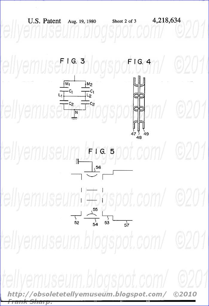
FIG. 3 shows an equivalent circuit of the electron gun of FIG. 2;
FIG. 4 is a sectional view of a modification of a fourth focusing grid used with the electron gun of FIG. 2;
FIG. 5 schematically illustrates a modification of the electron gun of FIG. 1; and
FIG. 6 is a sectional view of an electron gun according to another embodiment of this invention.
DESCRIPTION OF THE PREFERRED EMBODIMENTS
For an electron gun embodying this in vention,
there is applied an entirely novel process never known to date which
utilizes an electrostatic capacity of an electrode to apply voltage
on said electrode. Therefore, an electron lens can be designed to act
as a high voltage electrode, though actually a much lower voltage is
externally applied.
vention,
there is applied an entirely novel process never known to date which
utilizes an electrostatic capacity of an electrode to apply voltage
on said electrode. Therefore, an electron lens can be designed to act
as a high voltage electrode, though actually a much lower voltage is
externally applied.
There will now be described by reference to the accompanying drawing the cases where this invention is applied to a uni-potential type electron gun and a bi-potential type electron gun. Description is first given of the case where this invention is applied to the uni-potential type electron gun. FIGS. 1A, 1B and 2 are respectively a front view, plan view and sectional view of an in-line type electron gun used with a color picture tube. An electron gun 1 comprises a plurality of electrodes and glass supports thereof. The plural electrodes constitute these cathodes 2, 3, 4, first grid 5, second grid 6, third grid or first focusing grid 7, fourth grid or third focusing grid 8 and fifth grid or second focusing grid 9. These grids are fitted to the glass supports 10 in the order mentioned as counted from the cathode side. The cathodes 2, 3, 4, send forth electron beams along three paths lying on the same plane. The first grid 5 and second grid 6 are flat electrodes closely facing each other and are respectively bored with a group of three openings 11-12-13 and another group of three openings 14-15-16 which are aligned with the three electron beam paths. The third grid or first focusing grid 7 is positioned adjacent to the second grid 6. The grid 7 is formed of a pair of cups 20, 21 joined with each other on the peripheral edges of the openings thereof. The bottoms of said cups 20, 21 are respectively bored with a group of three openings 17-18-19 and another group of three openings 22, 23, 24 which are aligned with the three electron beam paths. The openings 17, 18, 19 of the first cup 20 have a larger diameter than the openings 14, 15, 16 of the second grid 6. The openings 22, 23, 24 of the second cup 21 have a larger diameter than the openings 17, 18, 19 of the first cup 20. The fourth grid or third focusing grid 8 is formed of at least three auxiliary electrodes 25, 26, 27. The first electrode 25 and third electrode 27 are respectively formed of a pair of cups joined with each other. Both electrodes 25, 27 are respectively bored with a group of three openings 28-29-30 and another group of three openings 33-34-35 which are aligned with the three electron beam paths. Said electrodes 25, 27 are electrically connected together to have the same potential, and spatially arranged along the electron beam paths. Provided between the electrodes 25, 27 is a plate-shaped second electrode 26, which is also bored with three openings aligned with the three electron beam paths. The fifth grid or second focusing grid 9 is cup-shaped, spaced from the fourth grid 8 substantially as much as a distance between the third grid 7 and fourth grid 8, and also bored with three openings 36, 37, 38. The central opening 37 is aligned with the axis 43 of the central opening of the first grid 5 to that of the fourth grid 8. But the other openings 36, 38 are respectively slightly displaced outward from the axes 44 of the side openings of the first grid 5 to that of the fourth grid 8. The displacement is intended to cause two electron beams other than the central one to be slightly deflected by an asymmetrical electric field in order to converge the three electron beams at a single point on a target. The fifth grid or second focusing grid 9 is fitted with a cylindrical shield cup 42 whose bottom is bored with three openings aligned with the three electron beam paths. A plurality of bulb spacers 45 made of a metal strip are mounted on the edge of the open side of the cylindrical shield cup 42.
The grids of the electron gun are spaced from each other as follows.
The third grid 7 and fifth grid 9 are electrically
connected together to have the same potential. The second electrode
26 of the fourth grid 8 is electrically insulated from the first
electrode 25 and third electrode 27 of said fourth grid 8, and is set
at a grounding potential or externally applied with a prescribed
value of voltage when the electron gun is put into operation.
However, the first electrode 25 and third electrode 27 of said fourth
grid 8 are not externally supplied with any voltage.
When an electron gun is built in a picture tube, the bulb spacers 45 are pressed against the inner wall of the picture tube, thereby electrically connecting the fifth grid 9 to the inner wall of the picture tube. During the operation of the electron gun, the third grid 7 and fifth grid 9 are applied with voltage of about 25 to 30 kv through the inner wall of the picture tube. The second electrode 26 of the fourth grid 8 is grounded through the base portion of the picture tube. At the time, the first electrode 25 and third electrode 27 of the fourth grid 8 are naturally applied with voltage of about 10 kv. The reason why this voltage is naturally generated in the first and third electrodes 25, 27 of the fourth grid 8 may be explained as follows by reference to the equivalent circuit of FIG. 3.
Two capacitors C 1
of FIG. 3 are respectively formed between the third grid 7 and the
first electrode 25 of the fourth grid 8, and also between the third
electrode 27 of the fourth grid 8 and fifth grid 9. Two other
capacitors C 2 are produced between the first and second
electrodes 25, 26 of the fourth grid 8, and also between the second
and third electrodes 26, 27 of said fourth grid 8.
C 1
of FIG. 3 are respectively formed between the third grid 7 and the
first electrode 25 of the fourth grid 8, and also between the third
electrode 27 of the fourth grid 8 and fifth grid 9. Two other
capacitors C 2 are produced between the first and second
electrodes 25, 26 of the fourth grid 8, and also between the second
and third electrodes 26, 27 of said fourth grid 8.
Referring to the equivalent circuit of FIG. 3, the two capacitors C 1 and the two other capacitors C 2 are respectively connected in series. The character M 1 denotes the third grid 7; the character M 2 the fifth grid 9; the charactor L 1 the first electrode 25; the character L 2 the third electrode 27; and the character N the second electrode 26. Where voltage of, for example, 25 kv is applied on the third grid 7 or M 1 and the fifth grid 9 or M 2 , and the second electrode 26 or N is set at a grounding potential, then voltage corresponding to the capacities of two capacitors C 1 , C 2 constituting one set is generated in the first electrode 25 or L 1 , and voltage corresponding to the capacities of two capacitors C 1 , C 2 constituting another set is generated in the third electrode 27 or L 2 . The capacities of the capacitors C 1 , C 2 are defined only by a distance between the respective electrodes constituting said capacitors, if the electrodes have substantially the same shape. Where, therefore, levels of voltage being applied on the first and third electrodes 25, 27 of the fourth grid 8 are selected in designing an electron gun, then a ratio which a distance between the electrodes constituting the capacitor C 1 bears to a distance between the electrodes constituting the capacitor C 2 is defined. Conversely speaking, where the ratio between said distances is chosen, then values of voltage applied on the first and third electrodes 25, 27 of the fourth grid 8 are determined. Values of the above-mentioned voltage and distance are practically decided as follows. An electron gun in which all the electrodes constituting the fourth grid 8 have the same potential represents the ordinary uni-potential type. Where this type of electron gun is designed by setting the focusing voltage (voltage impressed on the fourth grid 8) at 10 kv when voltage of 25 kv is applied on the third and fifth grids 7, 9, then it is advised to set a distance between the first and second electrodes 25, 26 of the fourth grid 8 and that between the second and third electrodes 26, 27 thereof and ground the second electrode 26. Assuming that a distance between the third grid 7 and first electrode 25, and a distance between the fifth grid 9 and third electrode 27, that is, distances between the electrodes respectively constituting the two capacitors C 1 are chosen to be 1 mm, then a distance between the first and second electrodes 25, 26 of the fourth grid 8 and a distance between the second and third electrodes 26, 27 thereof, that is, distances between the electrodes respectively constituting the two other capacitors C 2 are calculated to be 0.67 mm, as measured from the following equation: ##EQU1##
What should be taken into consideration in adopting the above-mentioned method of designing an electron gun, is to prevent the potential of the second electrode 26 of the fourth grid 8 from exerting a harmful effect on an electron lens. Namely, it is necessary, for example, to bore the second electrode 26 of the fourth grid 8 with three openings larger than those of the first and third electrode 25, 27 thereof and, where required, construct the fourth grid 8 as illustrated in FIG. 4, thereby preventing an electrostatic field created by the second electrode 26 from substantially exerting a harmful effect on the function of an electron gun particularly, an electron lens. The fourth grid of FIG. 4 is formed of a first electrode 47, second electrode 48 and third electrode 49. The peripheral edges of the three openings bored in the first electrode 47 and those of the third electrode 49 projects towrard the second electrode 48. If however, an electrostatic field generated in the neighborhood of the second electrode does not substantially exert any harmful effect on the function of an electron lens, then it is unnecessary to construct the fourth grid 8 as shown in FIG. 4. It is obviously possible positively to utilize an electrostatic field produced in the proximity of the second electrode 48. In such case, the interelectrode distance can not be determined by the previously described method.
Rigidly speaking, an electrostatic capacity is not defined solely by a distance between two mutually facing electrodes or other factors thereof, but is actually affected by the properties of other electrodes and earth capacity. Practically, therefore, a proper interelectrode distance has to be experimentally determined.
FIG.
5 schematically shows the arrangement of a modification of focusing
means used with an electron gun embodying this invention. This
focusing means is formed of a first focusing grid 52, second focusing
grid 53 and third focusing grid 54. The first focusing grid 52 is
bored with three openings aligned with three electron beam paths. The
second focusing grid 53 is bored, like the first focusing grid 52,
with three openings aligned with three electron beam paths, and
further fitted with a shield cup 57. The third focusing grid 54 is
formed of an inner annular auxiliary electrode 55 disposed
substantially halfway between the first and second focusing grids 52,
53 along an electron beam path and an outer annular auxiliary
electrode 56 positioned coaxially with the inner annular auxiliary
electrode 55 spatially to surround it. The inner annular auxiliary
electrode 55 is not externally impressed with voltage. The outer
annular auxiliary electrode 56 is set at a grounding potential. With
the focusing means of the above-mentioned construction, the potential
of the inner annular auxiliary electrode 55 is substantially defined
by an electrostatic capacity generated between the first and second
focusing grids 52, 53 and an electrostatic capacity produced between
the inner annular auxiliary electrode 55 and outer annular auxiliary
electrode 56.
The foregoing description relates to the case where this invention was applied to a uni-potential type electron gun. There will now be described by reference to FIG. 6 the case where the invention is applied to a bi-potential type electron gun. The electron gun of FIG. 6 comprises a cathode 60, first grid 61, second grid 62, first focusing grid 63 and second focusing grid 64 which are arranged in the order mentioned as counted from the cathode side, and each bored with one opening aligned with a common electron beam path. The first focusing grid 63 is formed of at least three electrodes, namely, first electrode 65, second electrode 66 and third electrode 67. With a bi-potential type electron gun constructed as described above, the second focusing grid 64 is applied with the final electron beam-accelating voltage (for example, 25 kv) of a picture tube. The second grid 62 is generally applied with voltage of about 500 v. With the ordinary bi-potential type electron gun, the first focusing grid 63 is applied with voltage of 3 to 4 kv. With a bi-potential type electron gun embodying this invention, however, it is only necessary to impress low voltage of, for example, 500 v or grounding voltage on the second electrode 66 and connect together the first and third electrodes 65, 67 disposed on both sides of the second electrode 66 with the same potential. Namely, the first and third electrodes 65, 67 are not externally impressed with any voltage. The potential of the mutually connected first and third electrodes 65, 67 is defined by the potentials of the second focusing grid 64, second electrode 66 and second grid 62 and the capacitances C 1 , C 2 , C 3 , C 4 generated between the respective electrodes (FIG. 6). The interelectrode distance is determined by the similar method to the aforementioned embodiment. Since the capacitances C 1 to C 4 vary with the shape of the corresponding electrodes, it should be defined with said variation taken into account.
With the bi-potential type electron gun of FIG. 6 embodying this invention, a sort of uni-potential electrostatic lens is formed in the first focusing grid 63. Therefore, electron beams are subjected to a certain degree of focusing while passing through the openings of the first focusing grid 63, thereby improving the focusing property of the bi-potential type electron gun of FIG. 6 over that of a similar type of electron gun in which the above-mentioned uni-potential electrostatic lens is not produced. Unless required, it is obviously possible to change that portion of the first focusing grid 63 in which the above-mentioned uni-potential electrostatic lens is produced into such shape as prevents electron beams from being focusing.
As described above, this invention makes it possible to elevate electron lens-forming voltage whose level has hitherto been subject to certain limitations due to requirements associated with the construction of a picture tube, thereby improving the function of the electron lens.
Namely, with the electron gun of this invention, high electrode voltage is indeed applied to increase the performance of an electron lens. To this end, however, much lower voltage has only to be externally applied, thereby eliminating arcings at the base portion of a picture tube which have hitherto raised problems. Further advantages of the invention are that since an external power source need not generate high voltage, the arrangement of a picture tube circuit
is simplified, decreasing the power consumption of said circuit; and
since the base portion of the picture tube is not applied with high
voltage, the picture tube can be operated more reliably, making it
possible to design the base portion so as to ensure the reduction of
cost. With the first embodiment of FIG. 2 relative to a uni-potential
type electron gun, the second electrode 26 was set at a grounding
potential. With the second embodiment of FIG. 6 relative to a
bi-potential type electron gun, the second electrode 66 is impressed
with low voltage of, for example, 500 v. With either type of electron
gun, the second electrode may be set at a grounding potential or be
impressed with low voltage. Where, as show in FIG. 6, the second
electrode is set at a grounding potential, provision of a variable
capacitor 68 between the second electrode 66 and the grounding electrode
outside of the picture tube makes it possible to control focusing
voltage, if necessary. Further, insertion of a high resister between
the second electrode and grounding electrode, though not changing the
focusing voltage, has the advantage that should a arcing take place
in a picture tube, said high resistor acts as a damping resistor,
minimising the generation of arc current and saving the cathode from
damage and other difficulties.
not generate high voltage, the arrangement of a picture tube circuit
is simplified, decreasing the power consumption of said circuit; and
since the base portion of the picture tube is not applied with high
voltage, the picture tube can be operated more reliably, making it
possible to design the base portion so as to ensure the reduction of
cost. With the first embodiment of FIG. 2 relative to a uni-potential
type electron gun, the second electrode 26 was set at a grounding
potential. With the second embodiment of FIG. 6 relative to a
bi-potential type electron gun, the second electrode 66 is impressed
with low voltage of, for example, 500 v. With either type of electron
gun, the second electrode may be set at a grounding potential or be
impressed with low voltage. Where, as show in FIG. 6, the second
electrode is set at a grounding potential, provision of a variable
capacitor 68 between the second electrode 66 and the grounding electrode
outside of the picture tube makes it possible to control focusing
voltage, if necessary. Further, insertion of a high resister between
the second electrode and grounding electrode, though not changing the
focusing voltage, has the advantage that should a arcing take place
in a picture tube, said high resistor acts as a damping resistor,
minimising the generation of arc current and saving the cathode from
damage and other difficulties.
The first embodiment relates to a uni-potential type electron gun provided with three in-line cathodes. The second embodiment relates to a bi-potential type electron gun comprising a single cathode. Obviously the type of electron gun and that of cathode can be freely combined. The point is that this invention is applicable to any type of electron gun, provided the focusing electrode or grid can be used as a capacitor type. With the foregoing embodiments, electrodes aligned with electron beam paths were utilized as the capacitor electrodes. However, application of this invention need not be limited to such type of electron gun. Namely, the electron gun of, for example, FIG. 2 may comprise a second cylindrical electrode which encloses a fourth grid and is bored with three openings aligned with three electron beam paths. In this case, an electron lens has its inner diameter reduced. Therefore, the electron lens should be constructed in consideration of the result of comparison between the effect of the voltage supplied thereto and the effect of the inner diameter thereof. Obviously, this invention is applicable to a tri-potential type electron gun.
This invention relates to an electron gun for generating one or more electron beams and more particularly to an electron gun provided with means for effectively focusing the electron beams on a target.
With the ordinary color picture tube provided with a multi-beam electron gun designed to generate a plurality of electron beams, the respective electron beams pass through separate electron lenses to be focussed at a point on a target. The electron lens is generally formed of a static electric field to focus the electron beams at a single point. The static electric field is formed at right angles to an electron beam path, and is disposed between at least two electrodes each bored with an opening allowing the passage of an electron beam. The properties of the electron lens can generally be varied according to interelectrode voltage, the size of an opening bored in the electrodes and a distance therebetween.
The electron gun is generally regarded to have a more improved performance, according as the electron lens is more reduced in the degree of magnification and spherical aberration. To provide an electron gun of high quality, therefore, it is necessary to extend the focal length of the electron lens. The most effective process to attain this object is to vary interelectrode voltage. However, the level of the interelectrode voltage should generally be restricted to fall within such a range as prevents arcing from taking place at the base portion of a picture tube. Further, enlargement of an electrode opening to extend the focal length of the electron lens is subject to certain limitations, because the neck diameter of the picture tube is restricted by other electrical requirements. Moreover, extension of the interelectrode distance is not advisable since the properties of the electron lens are harmfully affected by a electric charge occurring in the neck portion of the picture tube and the generation of an unnecessary electric field in the electron gun. As mentioned above, the design of the electron lens is subject to limitations due to various physical requirements associated with the construction of a picture tube. These limitation are particularly rigid in the case of a color picture tube using a multi-beam electron gun.
The customary process of manufacturing an electron lens having a long focal length without being obstructed by the above-mentioned limitations is to combine properly interelectrode voltage and the kind of electrode. An electron gun constructed by the above-mentioned process has already beam set forth in the Japanese patent disclosures Nos. 76072/1976 and 77061/1976.
However, the disclosed
processes have the drawbacks that the electron gun unavoidably has a
complicated construction and extra voltage has to be applied to
improve the formation of an electron lens, thus leading to economic
disadvantage. For elevation of the performance of an electron lens, it
is necessary
to apply high voltage with respect to not only the electron guns
used in the above-mentioned disclosed processes but also electron
guns in general use. In such a case, a special device has to be
provided to suppress arcing which might otherwise occur in the base
portion of a picture tube in order to ensure its reliable operation,
thus rendering the picture tube more expensive. SUMMARY OF THE INVENTION
It is accordingly the object of this invention to provide an electron gun admitting of the elevation of the performance of an electron lens without being obstructed by requirements associated with the construction of a picture tube.
According to this invention, there is provided an electron gun comprising a plurality of focusing grids spatially arranged along the path of an electron beam generated from a cathode and each bored with at least one opening for allowing the passage of the electron beam, wherein at least one of said plural focusing grids is formed of at least one electrode set at a grounding potential or a lower potential than the focusing voltage and at least one more electrode whose potential is defined by an electrostatic capacity.
BRIEF DESCRIPTION OF THE DRAWING
FIG. 1A is a front view of an electron gun according to one embodiment of this invention;
FIG. 1B is a plan view of the electron gun of FIG. 1A;
FIG. 2 is a sectional view of the electron gun of FIG. 1A;
FIG. 3 shows an equivalent circuit of the electron gun of FIG. 2;
FIG. 4 is a sectional view of a modification of a fourth focusing grid used with the electron gun of FIG. 2;
FIG. 5 schematically illustrates a modification of the electron gun of FIG. 1; and
FIG. 6 is a sectional view of an electron gun according to another embodiment of this invention.
DESCRIPTION OF THE PREFERRED EMBODIMENTS
For an electron gun embodying this in
 vention,
there is applied an entirely novel process never known to date which
utilizes an electrostatic capacity of an electrode to apply voltage
on said electrode. Therefore, an electron lens can be designed to act
as a high voltage electrode, though actually a much lower voltage is
externally applied.
vention,
there is applied an entirely novel process never known to date which
utilizes an electrostatic capacity of an electrode to apply voltage
on said electrode. Therefore, an electron lens can be designed to act
as a high voltage electrode, though actually a much lower voltage is
externally applied. There will now be described by reference to the accompanying drawing the cases where this invention is applied to a uni-potential type electron gun and a bi-potential type electron gun. Description is first given of the case where this invention is applied to the uni-potential type electron gun. FIGS. 1A, 1B and 2 are respectively a front view, plan view and sectional view of an in-line type electron gun used with a color picture tube. An electron gun 1 comprises a plurality of electrodes and glass supports thereof. The plural electrodes constitute these cathodes 2, 3, 4, first grid 5, second grid 6, third grid or first focusing grid 7, fourth grid or third focusing grid 8 and fifth grid or second focusing grid 9. These grids are fitted to the glass supports 10 in the order mentioned as counted from the cathode side. The cathodes 2, 3, 4, send forth electron beams along three paths lying on the same plane. The first grid 5 and second grid 6 are flat electrodes closely facing each other and are respectively bored with a group of three openings 11-12-13 and another group of three openings 14-15-16 which are aligned with the three electron beam paths. The third grid or first focusing grid 7 is positioned adjacent to the second grid 6. The grid 7 is formed of a pair of cups 20, 21 joined with each other on the peripheral edges of the openings thereof. The bottoms of said cups 20, 21 are respectively bored with a group of three openings 17-18-19 and another group of three openings 22, 23, 24 which are aligned with the three electron beam paths. The openings 17, 18, 19 of the first cup 20 have a larger diameter than the openings 14, 15, 16 of the second grid 6. The openings 22, 23, 24 of the second cup 21 have a larger diameter than the openings 17, 18, 19 of the first cup 20. The fourth grid or third focusing grid 8 is formed of at least three auxiliary electrodes 25, 26, 27. The first electrode 25 and third electrode 27 are respectively formed of a pair of cups joined with each other. Both electrodes 25, 27 are respectively bored with a group of three openings 28-29-30 and another group of three openings 33-34-35 which are aligned with the three electron beam paths. Said electrodes 25, 27 are electrically connected together to have the same potential, and spatially arranged along the electron beam paths. Provided between the electrodes 25, 27 is a plate-shaped second electrode 26, which is also bored with three openings aligned with the three electron beam paths. The fifth grid or second focusing grid 9 is cup-shaped, spaced from the fourth grid 8 substantially as much as a distance between the third grid 7 and fourth grid 8, and also bored with three openings 36, 37, 38. The central opening 37 is aligned with the axis 43 of the central opening of the first grid 5 to that of the fourth grid 8. But the other openings 36, 38 are respectively slightly displaced outward from the axes 44 of the side openings of the first grid 5 to that of the fourth grid 8. The displacement is intended to cause two electron beams other than the central one to be slightly deflected by an asymmetrical electric field in order to converge the three electron beams at a single point on a target. The fifth grid or second focusing grid 9 is fitted with a cylindrical shield cup 42 whose bottom is bored with three openings aligned with the three electron beam paths. A plurality of bulb spacers 45 made of a metal strip are mounted on the edge of the open side of the cylindrical shield cup 42.
The grids of the electron gun are spaced from each other as follows.
| ______________________________________ |
| A distance between the third grid or first focusing grid 7 and the first electrode 25 of the fourth grid or about 1 mm third focusing grid 8 A distance between the third electrode 27 of the fourth grid or third focusing about 1 mm grid 8 and the fifth grid or second focusing grid 9 A distance between the second electrode 26 and the first electrode 25 of the about 0.6 mm fourth grid or third focusing grid 8 A distance between the second electrode 26 and the third electrode 27 of the about 0.6 mm fourth grid or third focusing grid 8 |
| ______________________________________ |
When an electron gun is built in a picture tube, the bulb spacers 45 are pressed against the inner wall of the picture tube, thereby electrically connecting the fifth grid 9 to the inner wall of the picture tube. During the operation of the electron gun, the third grid 7 and fifth grid 9 are applied with voltage of about 25 to 30 kv through the inner wall of the picture tube. The second electrode 26 of the fourth grid 8 is grounded through the base portion of the picture tube. At the time, the first electrode 25 and third electrode 27 of the fourth grid 8 are naturally applied with voltage of about 10 kv. The reason why this voltage is naturally generated in the first and third electrodes 25, 27 of the fourth grid 8 may be explained as follows by reference to the equivalent circuit of FIG. 3.
Two capacitors
 C 1
of FIG. 3 are respectively formed between the third grid 7 and the
first electrode 25 of the fourth grid 8, and also between the third
electrode 27 of the fourth grid 8 and fifth grid 9. Two other
capacitors C 2 are produced between the first and second
electrodes 25, 26 of the fourth grid 8, and also between the second
and third electrodes 26, 27 of said fourth grid 8.
C 1
of FIG. 3 are respectively formed between the third grid 7 and the
first electrode 25 of the fourth grid 8, and also between the third
electrode 27 of the fourth grid 8 and fifth grid 9. Two other
capacitors C 2 are produced between the first and second
electrodes 25, 26 of the fourth grid 8, and also between the second
and third electrodes 26, 27 of said fourth grid 8. Referring to the equivalent circuit of FIG. 3, the two capacitors C 1 and the two other capacitors C 2 are respectively connected in series. The character M 1 denotes the third grid 7; the character M 2 the fifth grid 9; the charactor L 1 the first electrode 25; the character L 2 the third electrode 27; and the character N the second electrode 26. Where voltage of, for example, 25 kv is applied on the third grid 7 or M 1 and the fifth grid 9 or M 2 , and the second electrode 26 or N is set at a grounding potential, then voltage corresponding to the capacities of two capacitors C 1 , C 2 constituting one set is generated in the first electrode 25 or L 1 , and voltage corresponding to the capacities of two capacitors C 1 , C 2 constituting another set is generated in the third electrode 27 or L 2 . The capacities of the capacitors C 1 , C 2 are defined only by a distance between the respective electrodes constituting said capacitors, if the electrodes have substantially the same shape. Where, therefore, levels of voltage being applied on the first and third electrodes 25, 27 of the fourth grid 8 are selected in designing an electron gun, then a ratio which a distance between the electrodes constituting the capacitor C 1 bears to a distance between the electrodes constituting the capacitor C 2 is defined. Conversely speaking, where the ratio between said distances is chosen, then values of voltage applied on the first and third electrodes 25, 27 of the fourth grid 8 are determined. Values of the above-mentioned voltage and distance are practically decided as follows. An electron gun in which all the electrodes constituting the fourth grid 8 have the same potential represents the ordinary uni-potential type. Where this type of electron gun is designed by setting the focusing voltage (voltage impressed on the fourth grid 8) at 10 kv when voltage of 25 kv is applied on the third and fifth grids 7, 9, then it is advised to set a distance between the first and second electrodes 25, 26 of the fourth grid 8 and that between the second and third electrodes 26, 27 thereof and ground the second electrode 26. Assuming that a distance between the third grid 7 and first electrode 25, and a distance between the fifth grid 9 and third electrode 27, that is, distances between the electrodes respectively constituting the two capacitors C 1 are chosen to be 1 mm, then a distance between the first and second electrodes 25, 26 of the fourth grid 8 and a distance between the second and third electrodes 26, 27 thereof, that is, distances between the electrodes respectively constituting the two other capacitors C 2 are calculated to be 0.67 mm, as measured from the following equation: ##EQU1##
What should be taken into consideration in adopting the above-mentioned method of designing an electron gun, is to prevent the potential of the second electrode 26 of the fourth grid 8 from exerting a harmful effect on an electron lens. Namely, it is necessary, for example, to bore the second electrode 26 of the fourth grid 8 with three openings larger than those of the first and third electrode 25, 27 thereof and, where required, construct the fourth grid 8 as illustrated in FIG. 4, thereby preventing an electrostatic field created by the second electrode 26 from substantially exerting a harmful effect on the function of an electron gun particularly, an electron lens. The fourth grid of FIG. 4 is formed of a first electrode 47, second electrode 48 and third electrode 49. The peripheral edges of the three openings bored in the first electrode 47 and those of the third electrode 49 projects towrard the second electrode 48. If however, an electrostatic field generated in the neighborhood of the second electrode does not substantially exert any harmful effect on the function of an electron lens, then it is unnecessary to construct the fourth grid 8 as shown in FIG. 4. It is obviously possible positively to utilize an electrostatic field produced in the proximity of the second electrode 48. In such case, the interelectrode distance can not be determined by the previously described method.
Rigidly speaking, an electrostatic capacity is not defined solely by a distance between two mutually facing electrodes or other factors thereof, but is actually affected by the properties of other electrodes and earth capacity. Practically, therefore, a proper interelectrode distance has to be experimentally determined.
FIG.
5 schematically shows the arrangement of a modification of focusing
means used with an electron gun embodying this invention. This
focusing means is formed of a first focusing grid 52, second focusing
grid 53 and third focusing grid 54. The first focusing grid 52 is
bored with three openings aligned with three electron beam paths. The
second focusing grid 53 is bored, like the first focusing grid 52,
with three openings aligned with three electron beam paths, and
further fitted with a shield cup 57. The third focusing grid 54 is
formed of an inner annular auxiliary electrode 55 disposed
substantially halfway between the first and second focusing grids 52,
53 along an electron beam path and an outer annular auxiliary
electrode 56 positioned coaxially with the inner annular auxiliary
electrode 55 spatially to surround it. The inner annular auxiliary
electrode 55 is not externally impressed with voltage. The outer
annular auxiliary electrode 56 is set at a grounding potential. With
the focusing means of the above-mentioned construction, the potential
of the inner annular auxiliary electrode 55 is substantially defined
by an electrostatic capacity generated between the first and second
focusing grids 52, 53 and an electrostatic capacity produced between
the inner annular auxiliary electrode 55 and outer annular auxiliary
electrode 56. The foregoing description relates to the case where this invention was applied to a uni-potential type electron gun. There will now be described by reference to FIG. 6 the case where the invention is applied to a bi-potential type electron gun. The electron gun of FIG. 6 comprises a cathode 60, first grid 61, second grid 62, first focusing grid 63 and second focusing grid 64 which are arranged in the order mentioned as counted from the cathode side, and each bored with one opening aligned with a common electron beam path. The first focusing grid 63 is formed of at least three electrodes, namely, first electrode 65, second electrode 66 and third electrode 67. With a bi-potential type electron gun constructed as described above, the second focusing grid 64 is applied with the final electron beam-accelating voltage (for example, 25 kv) of a picture tube. The second grid 62 is generally applied with voltage of about 500 v. With the ordinary bi-potential type electron gun, the first focusing grid 63 is applied with voltage of 3 to 4 kv. With a bi-potential type electron gun embodying this invention, however, it is only necessary to impress low voltage of, for example, 500 v or grounding voltage on the second electrode 66 and connect together the first and third electrodes 65, 67 disposed on both sides of the second electrode 66 with the same potential. Namely, the first and third electrodes 65, 67 are not externally impressed with any voltage. The potential of the mutually connected first and third electrodes 65, 67 is defined by the potentials of the second focusing grid 64, second electrode 66 and second grid 62 and the capacitances C 1 , C 2 , C 3 , C 4 generated between the respective electrodes (FIG. 6). The interelectrode distance is determined by the similar method to the aforementioned embodiment. Since the capacitances C 1 to C 4 vary with the shape of the corresponding electrodes, it should be defined with said variation taken into account.
With the bi-potential type electron gun of FIG. 6 embodying this invention, a sort of uni-potential electrostatic lens is formed in the first focusing grid 63. Therefore, electron beams are subjected to a certain degree of focusing while passing through the openings of the first focusing grid 63, thereby improving the focusing property of the bi-potential type electron gun of FIG. 6 over that of a similar type of electron gun in which the above-mentioned uni-potential electrostatic lens is not produced. Unless required, it is obviously possible to change that portion of the first focusing grid 63 in which the above-mentioned uni-potential electrostatic lens is produced into such shape as prevents electron beams from being focusing.
As described above, this invention makes it possible to elevate electron lens-forming voltage whose level has hitherto been subject to certain limitations due to requirements associated with the construction of a picture tube, thereby improving the function of the electron lens.
Namely, with the electron gun of this invention, high electrode voltage is indeed applied to increase the performance of an electron lens. To this end, however, much lower voltage has only to be externally applied, thereby eliminating arcings at the base portion of a picture tube which have hitherto raised problems. Further advantages of the invention are that since an external power source need
 not generate high voltage, the arrangement of a picture tube circuit
is simplified, decreasing the power consumption of said circuit; and
since the base portion of the picture tube is not applied with high
voltage, the picture tube can be operated more reliably, making it
possible to design the base portion so as to ensure the reduction of
cost. With the first embodiment of FIG. 2 relative to a uni-potential
type electron gun, the second electrode 26 was set at a grounding
potential. With the second embodiment of FIG. 6 relative to a
bi-potential type electron gun, the second electrode 66 is impressed
with low voltage of, for example, 500 v. With either type of electron
gun, the second electrode may be set at a grounding potential or be
impressed with low voltage. Where, as show in FIG. 6, the second
electrode is set at a grounding potential, provision of a variable
capacitor 68 between the second electrode 66 and the grounding electrode
outside of the picture tube makes it possible to control focusing
voltage, if necessary. Further, insertion of a high resister between
the second electrode and grounding electrode, though not changing the
focusing voltage, has the advantage that should a arcing take place
in a picture tube, said high resistor acts as a damping resistor,
minimising the generation of arc current and saving the cathode from
damage and other difficulties.
not generate high voltage, the arrangement of a picture tube circuit
is simplified, decreasing the power consumption of said circuit; and
since the base portion of the picture tube is not applied with high
voltage, the picture tube can be operated more reliably, making it
possible to design the base portion so as to ensure the reduction of
cost. With the first embodiment of FIG. 2 relative to a uni-potential
type electron gun, the second electrode 26 was set at a grounding
potential. With the second embodiment of FIG. 6 relative to a
bi-potential type electron gun, the second electrode 66 is impressed
with low voltage of, for example, 500 v. With either type of electron
gun, the second electrode may be set at a grounding potential or be
impressed with low voltage. Where, as show in FIG. 6, the second
electrode is set at a grounding potential, provision of a variable
capacitor 68 between the second electrode 66 and the grounding electrode
outside of the picture tube makes it possible to control focusing
voltage, if necessary. Further, insertion of a high resister between
the second electrode and grounding electrode, though not changing the
focusing voltage, has the advantage that should a arcing take place
in a picture tube, said high resistor acts as a damping resistor,
minimising the generation of arc current and saving the cathode from
damage and other difficulties. The first embodiment relates to a uni-potential type electron gun provided with three in-line cathodes. The second embodiment relates to a bi-potential type electron gun comprising a single cathode. Obviously the type of electron gun and that of cathode can be freely combined. The point is that this invention is applicable to any type of electron gun, provided the focusing electrode or grid can be used as a capacitor type. With the foregoing embodiments, electrodes aligned with electron beam paths were utilized as the capacitor electrodes. However, application of this invention need not be limited to such type of electron gun. Namely, the electron gun of, for example, FIG. 2 may comprise a second cylindrical electrode which encloses a fourth grid and is bored with three openings aligned with three electron beam paths. In this case, an electron lens has its inner diameter reduced. Therefore, the electron lens should be constructed in consideration of the result of comparison between the effect of the voltage supplied thereto and the effect of the inner diameter thereof. Obviously, this invention is applicable to a tri-potential type electron gun.
Toshiba, "Blackstripe Vertical Stripe Screen Colour Picture Tube", 1973.


Claims:
I claim: 1. In a cathode ray tube including a faceplate and a shadow mask containing an array of vertically oriented slotted apertures for restricting electron beams directed therethrough to impinge upon and excite selected areas of phosphor material on said faceplate, a viewing screen comprising:
a horizontally repetitive pattern of sets of three vertically oriented stripes of phosphor material extending vertically across and coating the inside surface of said faceplate, each stripe within a set being of different phosphor material so as to emit a different color when excited by the corresponding one of the three electron beams passing through the associated aperture in said shadow mask, and a layer of light absorbing material coating the inside surface of said faceplate and containing a vertical and horizontal array of vertically oriented slotted openings, said stripes and openings being juxtaposed so that said openings define viewable portions of said stripes, each viewable portion being totally surrounded with light absorbing material,
said openings and stripes being aligned with the apertures in said shadow mask so that a corresponding one of said three electron beams is allowed to impinge upon each viewable portion,
the vertical dimension of each opening being greater than the vertical dimension of that part of said viewable portion excited by the electron beam impinging thereupon, such that a positive vertical guardband is provided, and
the horizontal dimension of each opening being less than the horizontal dimension of the impinging electron beam, such that a negative horizontal guardband is provided.
2. In a cathode ray tube including a faceplate and a shadow mask containing an array of vertically oriented slotted apertures for restricting electron beams directed therethrough to impinge upon and excite selected areas of phosphor material on said faceplate, a viewing
screen comprising:
a series of vertically oriented stripes of phosphor material extending across and coating the inside surface of said faceplate, the phosphor material of horizontally successive stripes differing in a repetitive pattern so as to emit different colors within each pattern when excited by electron beams, and
a layer of light absorbing material coating the inside surface of said faceplate in the form of a matrix comprising vertical stripes of material interposed between the phosphor stripes and horizontal spans of material crossing said phosphor stripes,
the vertical stripes and horizontal spans of light absorbing material defining the viewable portions of said phosphor stripes,
the vertical dimension of said horizontal spans being less than or equal to the vertical region of each phosphor stripe between vertically adjacent beam landings not excited by said electron beams, such that a zero to positive vertical guardband is provided for each viewable portion,
the horizontal dimension of the vertical stripes of light absorbing material being greater than the horizontal separation between horizontally adjacent phosphor stripes, such that a negative horizontal guardband is provided for each viewable portion.
3. In a cathode ray tube including a faceplace and a shadow mask containing an array of vertically oriented slotted apertures for restricting electron beams directed therethrough to land upon and excite selected areas of phosphor materials on said faceplate, a viewing screen comprising:
a layer of light absorbing material coating the inside surface of said faceplate and comprising a web containing an array of vertically oriented slotted openings therein, there being a unique set of three horizontally spaced openings for each aperture of said shadow mask aligned to receive the electron beams passing through said aperture, and
a layer of phosphor material coated on the inside surface of said faceplate within the boundaries of said openings, there being a different phosphor material for each of the openings of a set so as to emit a different color when excited by the electron beam impinging thereupon,
the height of said web between vertically adjacent sets of openings being less than or equal to the vertical distance between vertically adjacent beam landings to provide a zero to positive vertical guardband for each phosphor area,
the width of said web between horizontally adjacent openings being greater than the horizontal distance between horizontally adjacent beam landings to provide a negative horizontal guardband for each phosphor area.
I claim: 1. In a cathode ray tube including a faceplate and a shadow mask containing an array of vertically oriented slotted apertures for restricting electron beams directed therethrough to impinge upon and excite selected areas of phosphor material on said faceplate, a viewing screen comprising:
a horizontally repetitive pattern of sets of three vertically oriented stripes of phosphor material extending vertically across and coating the inside surface of said faceplate, each stripe within a set being of different phosphor material so as to emit a different color when excited by the corresponding one of the three electron beams passing through the associated aperture in said shadow mask, and a layer of light absorbing material coating the inside surface of said faceplate and containing a vertical and horizontal array of vertically oriented slotted openings, said stripes and openings being juxtaposed so that said openings define viewable portions of said stripes, each viewable portion being totally surrounded with light absorbing material,
said openings and stripes being aligned with the apertures in said shadow mask so that a corresponding one of said three electron beams is allowed to impinge upon each viewable portion,
the vertical dimension of each opening being greater than the vertical dimension of that part of said viewable portion excited by the electron beam impinging thereupon, such that a positive vertical guardband is provided, and
the horizontal dimension of each opening being less than the horizontal dimension of the impinging electron beam, such that a negative horizontal guardband is provided.
2. In a cathode ray tube including a faceplate and a shadow mask containing an array of vertically oriented slotted apertures for restricting electron beams directed therethrough to impinge upon and excite selecte
d areas of phosphor material on said faceplate, a viewing
screen comprising: a series of vertically oriented stripes of phosphor material extending across and coating the inside surface of said faceplate, the phosphor material of horizontally successive stripes differing in a repetitive pattern so as to emit different colors within each pattern when excited by electron beams, and
a layer of light absorbing material coating the inside surface of said faceplate in the form of a matrix comprising vertical stripes of material interposed between the phosphor stripes and horizontal spans of material crossing said phosphor stripes,
the vertical stripes and horizontal spans of light absorbing material defining the viewable portions of said phosphor stripes,
the vertical dimension of said horizontal spans being less than or equal to the vertical region of each phosphor stripe between vertically adjacent beam landings not excited by said electron beams, such that a zero to positive vertical guardband is provided for each viewable portion,
the horizontal dimension of the vertical stripes of light absorbing material being greater than the horizontal separation between horizontally adjacent phosphor stripes, such that a negative horizontal guardband is provided for each viewable portion.
3. In a cathode ray tube including a faceplace and a shadow mask containing an array of vertically oriented slotted apertures for restricting electron beams directed therethrough to land upon and excite selected areas of phosphor materials on said faceplate, a viewing screen comprising:
a layer of light absorbing material coating the inside surface of said faceplate and comprising a web containing an array of vertically oriented slotted openings therein, there being a unique set of three horizontally spaced openings for each aperture of said shadow mask aligned to receive the electron beams passing through said aperture, and
a layer of phosphor material coated on the inside surface of said faceplate within the boundaries of said openings, there being a different phosphor material for each of the openings of a set so as to emit a different color when excited by the electron beam impinging thereupon,
the height of said web between vertically adjacent sets of openings being less than or equal to the vertical distance between vertically adjacent beam landings to provide a zero to positive vertical guardband for each phosphor area,
the width of said web between horizontally adjacent openings being greater than the horizontal distance between horizontally adjacent beam landings to provide a negative horizontal guardband for each phosphor area.
Description:
This
invention relates to cathode ray tube screens, and more particularly to
black matrix screens for color television picture tubes employing
slotted aperture masks and a process for fabricating such screens.
Manufacturers
of cathode ray tubes of the color television picture tube type have
recently begun employing aperture masks having slotted apertures instead
of the more conventional circular apertures in order to achieve greater
electron beam transmission through the mask, since an array of slots in
an aperture mask allows the mask geometrically to be fabricated with
more total open area than the same size mask containing round or
circular apertures. The slotted apertures are typically arranged in
vertical columns on the mask, each column being comprised of a plurality
of slotted apertures. Since more electrons can impinge on the phosphor
regions of the screen in a tube of this type than of the circular
aperture, mask type, a brighter picture results. Unlike the
circularly-configured phosphor regions on the screen of a tube employing
an aperture mask having circular apertures, however, the phosphor
regions on the screen of a tube employing an aperture mask having
slotted apertures are formed in a pattern of adjacent vertical stripes,
typically with each stripe running continuously from the top of the
screen to the bottom.
Black
matrix tubes have also become widely popular as of late, both in
circular aperture mask tubes and slotted aperture mask tubes. As seen
from the viewing side of the screen of circular aperture mask tubes, the
black matrix material completely surrounds each circular phosphor dot,
serving to improve image contrast by absorbing ambient light that might
otherwise be reflected by the screen. Also as seen from the viewing side
of the screen of slotted aperture mask tubes, each vertical phosphor
stripe is separated from the adjacent vertical phosphor stripe by a
stripe of black matrix material running from the bottom to the top of
the screen.
In
fabricating screens for conventional slotted aperture mask tubes of the
black matrix type, a photoresist material coated over the inside
surface of a tube faceplate is exposed in a so-called lighthouse to
actinic radiation in a pattern corresponding to the pattern of matrix
openings ultimately to be formed on the screen. This radiation is
transmitted through the slotted apertures in the mask before impinging
on the photoresist material. The actinic light source used in this
fabrication process is linearly-elongated in a direction parallel to the
columns of slots in the aperture mask in order to permit the black
matrix material to be formed with a pattern of vertically and
horizontally-aligned, vertically-oriented slots extending between the
top and bottom of the screen. The phosphor stripes are thereafter
deposited so that phosphor of a predetermined color emission
characteristic, respectively, is deposited on the faceplate through a
predetermined slot, respectively. Three different phosphor materials are
conventionally deposited in a horizontally-repetitive pattern.
When
a screen formed in the aforementioned manner is operated in a color
television picture tube, parts of each of the phosphor stripes are not
excited by the electron beams, since electrons are blocked by the webs
of the mask between vertically-adjacent slots. These parts of the
stripes, therefore, are essentially useless in producing images, since
they provide no illumination on the face of the tube as a result of
direct bombardment by primary electrons. Moreover, the phosphor material
in these regions adds to overall reflectivity of the screen and hence
has a deleterious effect on image contrast. To overcome this problem,
the present invention contemplates substituting black matrix material to
be seen from the viewing side of the screen to avoid reflection from
the parts of the phosphor stripes not excited by the electron beams.
This may be accomplished by using a source of actinic radiation for
producing slotted openings in the black matrix material that is of
shorter length than the linear source of actinic radiation for producing
the phosphor stripes. The resulting increase in area of black matrix
material serves to reduce screen reflectivity and enhance contrast of
the displayed images. Moreover, by controlling vertical size of the mask
webs between vertically-adjacent openings in the black matrix material,
either a positive guardband or negative guardband mode of operation in
the vertical direction may be achieved.
Accordingly,
one object of the invention is to provide a new and improved color
television picture tube of the black matrix type exhibiting reduced
screen reflectivity and enhanced image contrast.
Another
object is to provide a color television picture tube of the slotted
aperture mask type having a screen, as seen from the viewing side,
formed of a plurality of vertically-oriented linear phosphor regions
completely surrounded by black matrix material.
Another
object is to provide a black matrix color television picture tube of
the slotted aperture mask type capable of operating in a positive or
negative guardband mode of operation in the vertical direction.
A
further object is to provide a black matrix color television picture
tube wherein the vertical guardband of the matrix is controlled to
enhance image contrast without reducing image brightness.
Another
object is to provide a method of fabricating a color television picture
tube of the black matrix type wherein exposures to different levels of
actinic radiation are employed sequentially in forming the picture tube
screen.
Briefly,
in accordance with a preferred embodiment of the invention, a viewing
screen is provided for a cathode ray tube. The tube includes a faceplate
and employs a shadow mask containing an array of vertically-oriented
slotted apertures for restricting electron beams directed therethrough
to impinge on, and excite, selected areas of phosphor material on the
faceplate. The viewing screen comprises a layer of light-absorbing
material coated over the inside surface of the faceplate, with the layer
including a pattern of vertically-elongated openings therein, and a
plurality of vertically-oriented stripes of phosphor material arranged
such that horizontally successive stripes are comprised of different
phosphor materials according to a repeating pattern. Each of the
stripes, respectively, is coated over substantially the entire area of
all the elongated openings situated essentially in separate vertical
alignment, respectively.
In
accordance with another preferred embodiment of the invention, a method
of forming on the faceplate of a cathode ray tube a viewing screen for a
high contrast color television picture tube of the slotted aperture
mask, black matrix type is described. The method comprises forming a
first layer of photosensitive material on the inside surface of the
faceplate and exposing the photosensitive material to actinic radiation
through slotted apertures in the mask from a first linear radiation
source of predetermined dimension along its longitudinal axis. The
longitudinal axis of the first source is maintained substantially
parallel to the longitudinal axis of the slotted apertures. The
unexposed regions of the first layer of photosensitive material are then
removed, and a layer of black matrix material is formed atop the first
layer of photosensitive material and the inside surface of the
faceplate. The exposed regions of the first layer of photosensitive
material and the black matrix material coated thereon are next removed,
leaving openings in the black matrix material. A second layer of
photosensitive material is formed atop the black matrix material coated
on the inside surface of the faceplate and atop the exposed portions of
the inside surface of the faceplate. The second layer of photosensitive
material carries a phosphor material either coated thereon or mixed
therein, emitting a characteristic color of light when excited by
electrons. This is followed by exposing the second layer of
photosensitive material to actinic radiation through the slotted
apertures from a second linear radiation source of dimension along its
longitudinal axis exceeding the predetermined dimension, the
longitudinal axis of the second source also being substantially parallel
to the longitudinal axis of the slotted apertures. The unexposed
regions of the second layer of photosensitive material are then removed.
In this fashion, phosphor material is applied over the inside surface
of the faceplate in registry with the openings in the black matrix
layer. If desired, the phosphor material may be applied in the form of
vertical stripes extending between the top and bottom of the screen by
increasing the length of the second radiation source, increasing the
duration of exposure therefrom, or a combination of both.
Deflection device for use in color television receiver:
Self convergent deflection system in color CRT TUBE TOSHIBA.
 A
deflection device for use in a color television receiver comprises a
deflection yoke fitted to a neck portion of the color television
receiver having three horizontally arranged electron guns so designed as
to emit three electron beams, for deflecting horizontally and
vertically said three electron beams emitted onto a fluorescent screen
from the electron guns of the color television receiver, and soft
magnetic material pieces fitted to an end portion of the deflection yoke
nearer to the screen, for locally varying the distribution of a
deflection field generated by the yoke so as to correct mis-convergence
of said three electron beams occurring at the peripheral portion of the
screen.
A
deflection device for use in a color television receiver comprises a
deflection yoke fitted to a neck portion of the color television
receiver having three horizontally arranged electron guns so designed as
to emit three electron beams, for deflecting horizontally and
vertically said three electron beams emitted onto a fluorescent screen
from the electron guns of the color television receiver, and soft
magnetic material pieces fitted to an end portion of the deflection yoke
nearer to the screen, for locally varying the distribution of a
deflection field generated by the yoke so as to correct mis-convergence
of said three electron beams occurring at the peripheral portion of the
screen.
1.
In a deflection device for use in a color television receiver, which
is fitted to a neck portion of a color picture tube having electron
guns emitting three electron beams, said electron guns being arranged
in a horizontal plane and which comprises a deflection yoke for
horizontally and vertically deflecting said three electron beams on a
screen and at least a soft magnetic material piece fitted on said
deflection yoke, the improvement which comprises a deflection yoke
which is so designed as to eliminate mis-convergences MC1, MC2, MC3, MC4 and MC7, in the mis-convergence MC1
the three electron beams being horizontally displaced from each other
at both the upper and lower end portions of the vertical or Y axis, in
the mis-convergence MC2, the three electron beams being
vertically displaced from each other at both the upper and lower end
portions of the Y axis, in the mis-convergence MC3, the three
electron beams being horizontally displaced from each other at both
the right and left end portions of the horizontal or X axis, in the
mis-convergence MC4 three electron beams being vertically
displaced from each other at both the right and left end portions of the
X axis, and in the mis-convergence MC7 scanning lines of
the three electron beams being vertically displaced at intermediate
portions between the Y axis and each of said right and left ends of the
screen; and at least a soft magnetic material piece fitted to an end
portion of said deflection yoke nearer to the screen of the color
picture tube so as only to eliminate a mis-convergence MC5
wherein the three electron beams are horizontally displaced from each
other at the diagonal end portions of the screen and a mis-convergence
MC6 wherein the three electron beams are vertically displaced from each other at the diagonal end portions of the screen.
2. A deflection device according to claim 1, wherein said soft magnetic piece defines an angle θ of 45° to 70° with a vertical line of the color picture tube.
3. A deflection device according to claim 1 wherein said soft magnetic material pieces are fitted at positions symmetrical with respect to each of two planes including therein the axial center of said deflection yoke and being in parallel with the horizontal and vertical deflecting directions, respectively.
4. A deflection device according to claim 1 wherein said soft magnetic material pieces have a configurational anisotropy.
5. A deflection device according to claim 1 wherein said soft magnetic material pieces are constructed so that at least either one of their configurational anisotropy and attachment position can be varied.
Self convergent deflection system in color CRT TUBE TOSHIBA.
 A
deflection device for use in a color television receiver comprises a
deflection yoke fitted to a neck portion of the color television
receiver having three horizontally arranged electron guns so designed as
to emit three electron beams, for deflecting horizontally and
vertically said three electron beams emitted onto a fluorescent screen
from the electron guns of the color television receiver, and soft
magnetic material pieces fitted to an end portion of the deflection yoke
nearer to the screen, for locally varying the distribution of a
deflection field generated by the yoke so as to correct mis-convergence
of said three electron beams occurring at the peripheral portion of the
screen.1.
In a deflection device for use in a color television receiver, which
is fitted to a neck portion of a color picture tube having electron
guns emitting three electron beams, said electron guns being arranged
in a horizontal plane and which comprises a deflection yoke for
horizontally and vertically deflecting said three electron beams on a
screen and at least a soft magnetic material piece fitted on said
deflection yoke, the improvement which comprises a deflection yoke
which is so designed as to eliminate mis-convergences MC1, MC2, MC3, MC4 and MC7, in the mis-convergence MC1
the three electron beams being horizontally displaced from each other
at both the upper and lower end portions of the vertical or Y axis, in
the mis-convergence MC2, the three electron beams being
vertically displaced from each other at both the upper and lower end
portions of the Y axis, in the mis-convergence MC3, the three
electron beams being horizontally displaced from each other at both
the right and left end portions of the horizontal or X axis, in the
mis-convergence MC4 three electron beams being vertically
displaced from each other at both the right and left end portions of the
X axis, and in the mis-convergence MC7 scanning lines of
the three electron beams being vertically displaced at intermediate
portions between the Y axis and each of said right and left ends of the
screen; and at least a soft magnetic material piece fitted to an end
portion of said deflection yoke nearer to the screen of the color
picture tube so as only to eliminate a mis-convergence MC5
wherein the three electron beams are horizontally displaced from each
other at the diagonal end portions of the screen and a mis-convergence
MC6 wherein the three electron beams are vertically displaced from each other at the diagonal end portions of the screen.
A
deflection device for use in a color television receiver comprises a
deflection yoke fitted to a neck portion of the color television
receiver having three horizontally arranged electron guns so designed as
to emit three electron beams, for deflecting horizontally and
vertically said three electron beams emitted onto a fluorescent screen
from the electron guns of the color television receiver, and soft
magnetic material pieces fitted to an end portion of the deflection yoke
nearer to the screen, for locally varying the distribution of a
deflection field generated by the yoke so as to correct mis-convergence
of said three electron beams occurring at the peripheral portion of the
screen.1.
In a deflection device for use in a color television receiver, which
is fitted to a neck portion of a color picture tube having electron
guns emitting three electron beams, said electron guns being arranged
in a horizontal plane and which comprises a deflection yoke for
horizontally and vertically deflecting said three electron beams on a
screen and at least a soft magnetic material piece fitted on said
deflection yoke, the improvement which comprises a deflection yoke
which is so designed as to eliminate mis-convergences MC1, MC2, MC3, MC4 and MC7, in the mis-convergence MC1
the three electron beams being horizontally displaced from each other
at both the upper and lower end portions of the vertical or Y axis, in
the mis-convergence MC2, the three electron beams being
vertically displaced from each other at both the upper and lower end
portions of the Y axis, in the mis-convergence MC3, the three
electron beams being horizontally displaced from each other at both
the right and left end portions of the horizontal or X axis, in the
mis-convergence MC4 three electron beams being vertically
displaced from each other at both the right and left end portions of the
X axis, and in the mis-convergence MC7 scanning lines of
the three electron beams being vertically displaced at intermediate
portions between the Y axis and each of said right and left ends of the
screen; and at least a soft magnetic material piece fitted to an end
portion of said deflection yoke nearer to the screen of the color
picture tube so as only to eliminate a mis-convergence MC5
wherein the three electron beams are horizontally displaced from each
other at the diagonal end portions of the screen and a mis-convergence
MC6 wherein the three electron beams are vertically displaced from each other at the diagonal end portions of the screen.2. A deflection device according to claim 1, wherein said soft magnetic piece defines an angle θ of 45° to 70° with a vertical line of the color picture tube.
3. A deflection device according to claim 1 wherein said soft magnetic material pieces are fitted at positions symmetrical with respect to each of two planes including therein the axial center of said deflection yoke and being in parallel with the horizontal and vertical deflecting directions, respectively.
4. A deflection device according to claim 1 wherein said soft magnetic material pieces have a configurational anisotropy.
5. A deflection device according to claim 1 wherein said soft magnetic material pieces are constructed so that at least either one of their configurational anisotropy and attachment position can be varied.
Description:
This
invention relates to a deflection device for use in a color television
receiver, used in a three-electron beam type color picture tube
wherein reproduction of a picture image is effected by causing three
electron beams corresponding to three primary colors of red, green and
blue to scan a fluorescent screen in both horizontal and vertical
directions while said three electron beams being allowed to impinge
upon said screen.
 The
three-electron beam type color picture tube should be so constructed
that when the three electron beams corresponding to red, green and blue
scan the fluorescent screen of the color picture tube, the rasters of
the three primary colors are overlapped by permitting the three electron
beams to be converged, for the purpose of preventing the occurrence of
color displacement due to mis-convergence of said three electron
beams. To this end, in a color picture tube of a so-called in-line
arranged beam system wherein three electron beams are emitted in a
state wherein they are arranged in a horizontal plane, electron guns 1,
3 at both opposite sides of a central electron gun 2 shown in FIG. 1
are usually disposed respectively horizontally inclined at prescribed
angles to the central electron gun. In an actually manufactured color
picture tube unit, however, three electron beams ER, EG and EB are not
always converged at one point due to a low accuracy with which the
electron guns are arranged, the effect of an external magnetic field,
etc. To solve this problem, a static convergence yoke 5 is usually
fitted to a neck portion 4 of the color picture tube and a so-called
static convergence is effected by this yoke 5 so as to permit the
three-electron beams to be completely converged at least at the screen
center.
The
three-electron beam type color picture tube should be so constructed
that when the three electron beams corresponding to red, green and blue
scan the fluorescent screen of the color picture tube, the rasters of
the three primary colors are overlapped by permitting the three electron
beams to be converged, for the purpose of preventing the occurrence of
color displacement due to mis-convergence of said three electron
beams. To this end, in a color picture tube of a so-called in-line
arranged beam system wherein three electron beams are emitted in a
state wherein they are arranged in a horizontal plane, electron guns 1,
3 at both opposite sides of a central electron gun 2 shown in FIG. 1
are usually disposed respectively horizontally inclined at prescribed
angles to the central electron gun. In an actually manufactured color
picture tube unit, however, three electron beams ER, EG and EB are not
always converged at one point due to a low accuracy with which the
electron guns are arranged, the effect of an external magnetic field,
etc. To solve this problem, a static convergence yoke 5 is usually
fitted to a neck portion 4 of the color picture tube and a so-called
static convergence is effected by this yoke 5 so as to permit the
three-electron beams to be completely converged at least at the screen
center.
Even in a color picture tube so constructed that the three electron beams ER, EB and EG are converged at the screen center by effecting the static convergence as above mentioned, in cases where the three electron beams are deflected by a deflection yoke 6 up to the peripheral portion of the screen, they fail to be converged at one point, that is, a mis-convergence occurs. The reason is that the three electron guns 1, 2 and 3 are disposed spatially separately from each other. In order to zero this mis-convergence, a dynamic convergence is generally carried out. For the purpose of effecting the dynamic convergence, as shown in, for example, FIG. 2, a pair of cores 7a, 7b are disposed, respectively, at both opposite sides of a neck portion 6 of the color picture tube and dynamic convergence windings 8a, 9a, 10a and 8b, 9b, 10b are wound, respectively, about said pair of cores, and a dynamic correcting current is supplied from a dynamic convergence control circuit 11 to said windings 8a, 8b, 9a, 9b, 10a and 10b. Note that in FIG. 2 reference numerals 12, 13 and 14, 15 denote permanent magnets for effecting a static convergence. The above-mentioned dynamic correcting current is made to have a suitable waveform so as to correct in accordance with the line scanning rate, field scanning rate, etc. the paths of the side beams ER and EB of the three electron beams (ER, EG, EB of FIG. 1) emitted from the electron guns 1, 2 and 3, in order to attain a sufficient convergence at all points of the screen. Accordingly, a circuit for supplying said correcting current, i.e., said dynamic convergence control circuit 11 generally becomes extremely complicated in construction and simultaneously the power consumption in this circuit 11 becomes large. In cases where, in a shadow mask type color receiving tube as presently widely used, a dynamic convergence is carried out, the incident angle of the three electron beams incident into the shadow mask is also varied as this dynamic convergence is effected. Accordingly, when it is desired to obtain a desired color purity, a correcting device used for light exposure in forming a fluorescent screen also becomes complicated.
The above-mentioned problems encountered where the dynamic convergence is carried out are becoming more and more remarkable with the widening of a deflection angle for the electron beams of the color picture tube (at present, there is a tendency that a wide-angled Braun tube of 110° or more is favourably used), or with application of higher anode voltage. In the case of, for example, a color picture tube 20 inch in screen size and 110° in electron beam-deflecting angle, the dynamic convergence control circuit 11 has 10 or more portions to be readjusted. In such a case, the manufacturer needs a long time to perform the convergence-correcting operation, which results in a costly color picture tube. Further, there is an inconvenience that difficulties are encountered in performing quickly and properly the above-mentioned readjustment upon a domestic replacement of the color picture tube.
The color picture tube of in-line arranged beam system is somewhat simplified in respect of the construction of its circuit device for effecting the above-mentioned dynamic convergence as compared with the conventionally widely used color picture tube of Δ-arranged beam system but if possible, it is strongly desired for the color picture tube to require no dynamic convergence-operation at all.
There have in recent years been contemplated various color picture tubes which eliminate the necessity of performing the dynamic convergence, for example, through making the magnetic field distribution of the deflection device appropriate and yet reducing the manufacturing errors. For example, U.S. Pat. No. 2,764,628 describes in its specification that three horizontally arranged electron beams are allowed to scan directly the fluorescent screen without being converged, and three primary color signals for modulating the three electron beams are delayed by a length of time corresponding to the interval between the three parallel emitted electron beams, thereby to prevent the color pictures from being subjected to color displacement. This system will indeed well serve the purpose if the deflection field is not distorted at all by the deflection yoke, but in the case of an actual deflection yoke it is impossible to zero the distortion of the deflection field. The color picture tube of this system, therefore, has no realizability.
 Under
these circumstances, the present inventors have contemplated a color
picture tube which does not have the above-mentioned drawbacks. As shown
in FIG. 3, in this color picture tube, the direction and position in
which the three electron guns 1, 2 and 3 are disposed are so determined
that electron beams ER, EG and EB emitted from the three electron guns
1, 2 and 3 are converged at a point outside of a fluorescent screen F. A
deflection yoke 6 for deflecting the three electron beams ER, EG and
EB is so designed as to generate a deflection field whose distribution
has an appropriate distortion. Three primary color signals for
modulating the three electron beams ER, EG and EB are respectively
delayed by a length of time corresponding respectively to the intervals
D between those points of the fluorescent screen F upon which the
three electron beams ER, EG and EB impinge at a point of time.
Accordingly, the three electron beams ER, EG and EB scan the
fluorescent screen under the requirements that they impinge upon a
given region of the fluorescent screen F substantially at prescribed
intervals, to permit each of phosphor dots provided on the fluorescent
screen to emit a necessary amount of fluorescent light. On the other
hand, the three primary color signals for modulating the three electron
beams ER, EG and EB are respectively given a prescribed length of
delay time in corresponding relationship to a length of time
corresponding to the above-mentioned intervals D. Thus, this color
picture tube exhibits the same function as that in the case where the
three electron beams ER, EG and EB scan the fluorescent screen while
being kept converged at one point of the fluorescent screen. The color
picture tube having the foregoing construction, however, still remains
to have the following problems.
Under
these circumstances, the present inventors have contemplated a color
picture tube which does not have the above-mentioned drawbacks. As shown
in FIG. 3, in this color picture tube, the direction and position in
which the three electron guns 1, 2 and 3 are disposed are so determined
that electron beams ER, EG and EB emitted from the three electron guns
1, 2 and 3 are converged at a point outside of a fluorescent screen F. A
deflection yoke 6 for deflecting the three electron beams ER, EG and
EB is so designed as to generate a deflection field whose distribution
has an appropriate distortion. Three primary color signals for
modulating the three electron beams ER, EG and EB are respectively
delayed by a length of time corresponding respectively to the intervals
D between those points of the fluorescent screen F upon which the
three electron beams ER, EG and EB impinge at a point of time.
Accordingly, the three electron beams ER, EG and EB scan the
fluorescent screen under the requirements that they impinge upon a
given region of the fluorescent screen F substantially at prescribed
intervals, to permit each of phosphor dots provided on the fluorescent
screen to emit a necessary amount of fluorescent light. On the other
hand, the three primary color signals for modulating the three electron
beams ER, EG and EB are respectively given a prescribed length of
delay time in corresponding relationship to a length of time
corresponding to the above-mentioned intervals D. Thus, this color
picture tube exhibits the same function as that in the case where the
three electron beams ER, EG and EB scan the fluorescent screen while
being kept converged at one point of the fluorescent screen. The color
picture tube having the foregoing construction, however, still remains
to have the following problems.
Usually, where, in the color picture tube of in-line arranged beam system, the three electron beams as emitted are deflected by the deflection yoke, they are mis-converged as shown in FIG. 4. That is to say, when it isassumed that a
horizontal one of two axes passing through a screen center and
intersecting at right angles to each other is represented by X and a
vertical one of said two axes by Y. Then, the following
mis-convergences occur. That is, a mis-convergence MC 1
wherein the three electron beams are horizontally displaced from each
other at both the upper and lower end portions of the Y axis and a
mis-convergence MC 2 wherein the three electron beams are
vertically displaced from each other at both the upper and lower end
portions of the Y axis, a mis-convergence MC 3 wherein the
three electron beams are horizontally displaced from each other at both
the right and left end portions of the X axis and a mis-convergence MC 4
wherein the three electron beams are vertically displaced from each
other at both the right and left end portions of the X axis, a
mis-convergence MC 5 wherein the three electron beams are
horizontally displaced from each other at the diagonal end portions of
the screen and a mis-convergence MC 6 wherein the three
electron beams are vertically displaced from each other at the diagonal
end portions of the screen, and a mis-convergence MC 7
wherein scanning lines at the proximities of both the upper and lower
ends of the screen coincide with each other at the respective
proximities of the Y axis and the right and left ends of the screen and
are vertically displaced at intermediate portions between the Y axis
and each of said right and left ends of the screen.
The MC 2 and MC 4 of the above-mentioned mis-convergence occur due to errors in arranging the electron guns, errors in attaching the deflection yokes, or unsymmetry of the deflection yokes, but can be adjusted by constructing an attaching mechanism for electron guns and an attaching mechanism for attaching deflection yokes to a color picture tube so that each of these mechanisms may have a correcting function. That is to say, said MC 2 and MC 4 can readily be corrected by simple adjusting mechanisms mounted on a conventional picture tube and deflection yoke.
The MC 1 can be removed by distorting into an appropriate barrel-configuration the distribution of a magnetic field produced by vertical deflection coils. The MC 3 can be removed by distorting into an appropriate pincushion-configuration the distribution of a magnetic field produced by horizontal deflection coils. Further, the MC 5 can be substantially zeroed by removing said MC 1 and MC 3 .
Where attempts are made to remove the MC 1 and MC 3 by varying the winding distribution of each deflection coil, either one of the MC 6 and MC 7 necessarily occurs, that is to say, it is impossible to remove both of them at the same time the MC 6 and MC 7 run counter to each other, that is, are related to each other in such a manner that if either one of them becomes small, the other becomes large. In the prior art, no attempt was made to completely remove any one of the MC 6 and MC 7 . That is, in the prior art, at ten or more portions of the color picture tube adjustment was so made as to permit the MC 6 and MC 7 to be equalized in degree with each other thereby to prevent occurrence of an extremely large mis-convergence, or alternatively arrangement was so made as to permit mis-convergences to occur at the peripheral portion of the screen where mis-convergences are relatively not outstanding. Accordingly, in the case of time indication or score display of baseball, a viewer has heretofore viewed a deteriorated picture image.
The above-mentioned reciprocal relationship between the MC 6 and MC 7 is established also in the case of the above-mentioned color picture tube of FIG. 3.
The object of the invention is to provide a deflection device for use in a color television receiver wherein soft magnetic material pieces having a configurational anisotropy, for example, rectangular soft iron pieces are fitted to the front end portion of a deflection yoke mounted on an in-line arranged three-electron beam type color picture tube, that is, to an end portion of the deflection yoke on the screenside, whereby the distribution of a deflection field produced by the deflection yoke is locally varied so as to correct the mis-convergence of in-line arranged three-electron beams occurring at four corners of the screen thus to achieve a good convergence over a substantially entire region of the screen.
According to the present invention there can be obtained a deflection device which comprises a deflection yoke fitted to a neck portion of a color picture tube provided with three electron guns emitting three electron beams in a state arranged in a horizontal plane, said deflection yoke being horizontally and vertically, and soft magnetic material pieces fitted to an end portion of the deflection yoke nearer to the screen, whereby the distribution of deflection field from the deflection yoke is varied by the soft magnetic material pieces to correct mis-convergences.
The present inventors have found that the above-mentioned mis-convergences MC 6 and MC 7 can be both removed at the same time if the following measures are taken. A first measures is to prepare vertical and horizontal deflection coils so designed that they can remove the MC 1 and MC 3 , respectively, and also remove the above MC 7 . With respect to the MC 6 occurring at corners of the screen as shown in FIG. 5, a magnetic material piece free from permanent magnetization, for example, a soft magnetic material piece 23 is fitted to the front end portion of a deflection yoke 21, that is, to a yoke holder 22 as shown in FIGS. 6A, 6B and 7, thereby to locally vary the distribution of deflecti on field, thus to remove the MC 6
utilizing the relative movement of the three electron beams made in
accordance with the variation of the deflection field distribution. If
arrangement is made as such, a dynamic convergence becomes unnecessary.
Therefore, a great advantage results. Note here that what is important
is that unless a material free from permanent magnetization is used as
said magnetic material piece, the effect of the invention can not be
obtained. This material should be magnetically soft, namely, is a soft
magnetic material. Have it in mind that it is important to locally vary
the distribution of magnetic field produced by the deflection yoke 21
so as to remove the MC 6 of FIG. 5 without affecting the
convergence at the remaining region of the screen, through adjusting the
size (width a, length b and thickness c), the attachment position (an
angle θ defined by the piece 23 with a vertical line Y in the case
where the piece 23 is fitted to the picture tube), or the attachment
angle (an inclined angle Ψ defined by the longitudinal axis of the
piece 23 with said vertical line Y) of the magnetic material piece 23.
on field, thus to remove the MC 6
utilizing the relative movement of the three electron beams made in
accordance with the variation of the deflection field distribution. If
arrangement is made as such, a dynamic convergence becomes unnecessary.
Therefore, a great advantage results. Note here that what is important
is that unless a material free from permanent magnetization is used as
said magnetic material piece, the effect of the invention can not be
obtained. This material should be magnetically soft, namely, is a soft
magnetic material. Have it in mind that it is important to locally vary
the distribution of magnetic field produced by the deflection yoke 21
so as to remove the MC 6 of FIG. 5 without affecting the
convergence at the remaining region of the screen, through adjusting the
size (width a, length b and thickness c), the attachment position (an
angle θ defined by the piece 23 with a vertical line Y in the case
where the piece 23 is fitted to the picture tube), or the attachment
angle (an inclined angle Ψ defined by the longitudinal axis of the
piece 23 with said vertical line Y) of the magnetic material piece 23.
This invention can be more fully understood from the following detailed description when taken in conjunction with the accompanying drawings, in which:
FIGS. 1 to 4 are intended to explain the object of the present invention,
FIG. 1 being a sectional view schematically showing a prior art color picture tube,
FIG. 2 showing a dynamic convergence means fitted to the prior art color picture tube,
FIG. 3 schematically showing a color picture tube wherein color displacement is corrected by giving a prescribed length of delay time to each of modulation signals of three electron beams without causing said three electron beams to be converged on a fluorescent screen of the color picture tube,
FIG. 4 being intended to explain mis-convergences in a color picture tube of in-line arranged beam system;
FIGS. 5 to 7 are intended to explain the fundamental principle of the present invention,
FIG. 5 showing the condition wherein mis-convergences occur only at four corners of the screen,
FIGS. 6A and 6B being respectively side and rear views showing the condition wherein a soft magnetic material piece is fitted to a deflection yoke,
FIG. 7 being a perspective view of the soft magnetic material piece; and
FIGS. 8 to 22 show an embodiment of the present invention,
FIG. 8 showing respective details of a shadow mask type color picture tube and a three-primary color signal supply section,
FIG. 9 showing the relations between inclined angles of electron beams and various values associated with said inclined angles,
FIGS. 10A and 10B being curve diagrams showing the distribution of deflection field from a horizontal deflection coil,
FIGS. 11A and 11B being curve diagrams showing the distribution of deflection field from a vertical deflection coil,
 FIGS.
12 and 13 showing respectively the variations in intensity of magnetic
fields produced from the horizontal and vertical deflection coils, as
viewed on the Z axes thereof,
FIGS.
12 and 13 showing respectively the variations in intensity of magnetic
fields produced from the horizontal and vertical deflection coils, as
viewed on the Z axes thereof,
FIG. 14 being intended to explain the positional displacement of three electron beams on the fluorescent screen,
FIGS. 15A and 15B being respectively side and rear views showing the condition wherein soft magnetic material pieces are fitted to a deflection yoke,
FIG. 16 being a perspective view of the soft magnetic material piece,
FIGS. 17A and 17B showing vertical and horizontal movements of the three electron beams relative to the variation of the attachment position of the soft magnetic material piece,
FIGS. 18A and 18B showing vertical and horizontal movements of the three electron beams relative to the variation of the attachment angle of the soft magnetic material piece,
FIGS. 19A, 19B, 19C, 19D, 19E, 19F, 20A, 20B, 20C, 20D, 20E and 20F showing individually vertical and horizontal movements of the three electron beams relative to the variation in width, length and thickness of a rectangular magnetic material piece,
FIG. 21 showing a detailed arrangement of a delay circuit,
FIG. 22 being intended to explain the operation of this embodiment.
FIG.
8 shows the detail of a shadow mask type color picture tube
constituting the main part of a color television receiver to which the
present invention is applied and the detail of a three-primary color
signal supply section for supplying three primary color signals to said
color picture tube. In FIG. 8, a glass bulb 31 is a vacuum envelope
having at its front portion a face plate 31a constituting a screen of
the color television receiver and at its rear portion a neck portion 31b
whose diameter is made small. In the inner surface of the face plate
31a of the glass bulb 31 is formed a fluorescent screen 32 on which are
arranged in a regular order phosphor dots which, when three electron
beams have impinged thereupon, emit three color television primary
colors of red (R), green (G) and blue (B). At a position a little
shifted from the surface of the fluorescent screen 32 toward the
incident side of the electron beams is disposed a shadow mask 33 having a
large number of small holes (not shown) corresponding to the phosphor
dots of the fluorescent screen 32. Within the neck portion 31b of the
glass bulb 31 are arranged three electron guns 34R, 34G and 34B, which
are in-line arranged horizontally to the screen. These electron guns
34R, 34G and 34B are so constructed as to emit toward the fluorescent
screen 32 three electron beams ER, EG and EB modulated by three primary
color signals SR, SG and SB as later described, respectively. Further,
these three electron guns 34R, 34G and 34B are arranged such that both
side-electron guns 34R and 34B are inclined in the same horizontal
plane at a prescribed angle α to the center electron gun 34G so as to
permit the three electron beams ER, EG and EB to be converged at one
point in a region outside of the fluorescent screen 32, that is,
outside of the face plate 31a. Since, as above described, a converged
point of the three electron beams ER, EG and EB is situated outside of
the fluorescent screen 32, these three electron beams impinge, at
intervals D, upon the surface of the fluorescent screen 32.
Further in detail, when α represents the inclined angle of the electron guns 34R, 34G and 34B, d represents the intervals between the three electron beams at the electron beam-emitting ends of the electron guns (in other words, the mutual intervals between the center positions of those ends of the electron guns from which to emit the electron beams ER, EG and EB), and L represents the distance between the forward, or electron beam-emitting end of the electron guns and the fluorescent screen 32, the mutual relation between said α, d and L is so determined as to satisfy the following inequality. d/6< d- Lα
That is to say, the difference between the interval d (mm) between the forward ends of the electron guns, and a product Lα obtained by multiplying the angle α (rad.) defined by both side-electron beams ER, EB with the center electron beam EG by the distance L between the forward end of the electron guns and the fluorescent film 32, namely, d-Lα, is so determined that it is greater than d/6 and smaller than d/2.
The d- Lα of the above inequality (1) is substantially equal to said interval D between the electron beam spots on the fluorescent screen 32. That is, since, as apparent from FIG. 9, tan α = (d- D)/L, D÷ d- Lα. In order to obtain a high resolution, it is preferred that 6.5 mm< d and that, in the case where the fluorescent screen size ranges from 14 inch-tube to 25 inch-tube, 1 mm< D< 5 mm.
For reference, a color picture tube manufactured for experimental use is of the following dimensions.
A deflection yoke 35 is fitted to the outer
periphery of the neck portion 31b of the glass bulb 31. This deflection
yoke 35 has horizontal and vertical deflection coils producing
magnetic fields for horizontally and vertically deflecting said three
electron beams ER, EG and EB. Said horizontal deflection coil is so
formed that a magnetic field distribution formed by this horizontal
deflection coil may assume a so-called pincushion shape wherein the
magnetic field intensity becomes gradually high as the measuring
position horizontally goes away from the axial center of the deflection
yoke 35. Said vertical deflection coil is so formed that a magnetic
field distribution formed by this vertical deflection coil may assume a
so-called barrel shape wherein the magnetic field intensity becomes
gradually low as the measuring position vertically goes away from the
axial center of the deflection yoke 35.
 FIGS.
10A and 10B are curve diagrams showing the magnetic field distribution
of a horizontal deflection coil 35H with a radially (horizontally)
shifted position from the axial center of the deflection yoke 35 plotted
on the abscissa and the magnetic field intensity (relative value)
plotted on the ordinate and a position on the Z axis of the deflection
yoke 35 taken as a parameter. In FIGS. 10A and 10B, however, numerical
values indicating the positions on the Z axis are defined as follows.
That is to say, Z = 0 (mm) is defined to indicate the position of the
forward end (the screen side) of the horizontal deflection coil, and
positive values (Z > 0) are defined to indicate positions shifted
forwardly of this position, that is, positions shifted toward the
screen while negative values (Z< 0) are defined to indicate
positions shifted rearwardly of that position, that is, positions going
away from the screen. At this time, the position of the rear end of the
horizontal deflection coil is represented by Z = -80 mm. Similarly,
FIGS. 11A and 11B are curve diagrams showing the magnetic field
distribution of a vertical deflection coil 35V with a radially
(vertically) shifted position from the axial center of the deflection
yoke 35 plotted on the abscissa and the magnetic field intensity
(relative value) plotted on the ordinate and a position on the Z axis of
the deflection yoke 35 taken as a parameter. Numerical values
indicating the positions on the Z axis are defined in the same manner as
in FIGS. 10A and 10B.
FIGS.
10A and 10B are curve diagrams showing the magnetic field distribution
of a horizontal deflection coil 35H with a radially (horizontally)
shifted position from the axial center of the deflection yoke 35 plotted
on the abscissa and the magnetic field intensity (relative value)
plotted on the ordinate and a position on the Z axis of the deflection
yoke 35 taken as a parameter. In FIGS. 10A and 10B, however, numerical
values indicating the positions on the Z axis are defined as follows.
That is to say, Z = 0 (mm) is defined to indicate the position of the
forward end (the screen side) of the horizontal deflection coil, and
positive values (Z > 0) are defined to indicate positions shifted
forwardly of this position, that is, positions shifted toward the
screen while negative values (Z< 0) are defined to indicate
positions shifted rearwardly of that position, that is, positions going
away from the screen. At this time, the position of the rear end of the
horizontal deflection coil is represented by Z = -80 mm. Similarly,
FIGS. 11A and 11B are curve diagrams showing the magnetic field
distribution of a vertical deflection coil 35V with a radially
(vertically) shifted position from the axial center of the deflection
yoke 35 plotted on the abscissa and the magnetic field intensity
(relative value) plotted on the ordinate and a position on the Z axis of
the deflection yoke 35 taken as a parameter. Numerical values
indicating the positions on the Z axis are defined in the same manner as
in FIGS. 10A and 10B.
 As
apparent from FIGS. 10A and 10B, in the region where the deflecting
magnetic field on the axial center (Z axis) of the deflection yoke 35
has an intensity of 1/2 the maximum value, the magnetic field
distribution of the horizontal deflection coil 35H assumes a pincushion
shape wherein the magnetic field intensity becomes gradually high as
the measuring position radially (horizontally) goes away from the Z
axis. As apparent from FIGS. 11A and 11B, the magnetic field
distribution of the vertical deflection coil 35V assumes a barrel shape
wherein the magnetic field intensity becomes gradually low as the
measuring position radially (vertically) goes away from the Z axis of
the deflection yoke 35.
As
apparent from FIGS. 10A and 10B, in the region where the deflecting
magnetic field on the axial center (Z axis) of the deflection yoke 35
has an intensity of 1/2 the maximum value, the magnetic field
distribution of the horizontal deflection coil 35H assumes a pincushion
shape wherein the magnetic field intensity becomes gradually high as
the measuring position radially (horizontally) goes away from the Z
axis. As apparent from FIGS. 11A and 11B, the magnetic field
distribution of the vertical deflection coil 35V assumes a barrel shape
wherein the magnetic field intensity becomes gradually low as the
measuring position radially (vertically) goes away from the Z axis of
the deflection yoke 35.
FIG.
12 shows for reference the variation of a horizontally deflecting
magnetic field intensity BH on the axial center (Z axis) of the
deflection yoke 35, and FIG. 13 similarly shows for reference the
variation of a vertically deflecting magnetic field intensity BV. The BH
curve of FIG. 12 corresponds to the magnetic field distribution curve
of FIGS. 10A and 10B while the BV curve of FIG. 13 corresponds to the
magnetic field distribution curve of  FIGS. 11A and 11B.
The main reason of using the deflection yoke 35 having the above-mentioned magnetic field distribution is to make zero any of both the difference YH- XH (this difference corresponds to said MC 1 ) where YH represents the interval between the electron beam spots at both the upper and lower ends of the screen and XH the interval between the electron beam spots at the center of the screen and the difference XH- XH' (this difference corresponds to said MC 3 ) where XH' represents the horizontal interval between the electron beam spots at both the right and left ends of the screen. Note that in FIG. 14 DV represents the vertical interval between the electron beam spots at both the right and left ends of the screen.
By the use of the deflection yoke 35 having the above-mentioned construction all the mis-convergences shown in FIG. 4 can be substantially removed except for said MC 6 , but through a complete removal of the MC 7 the MC 6 is relatively allowed to occur to an extent of about 1 mm. Hereinafter, how to zero this MC 6 is described.
 As
shown in FIG. 15A, to the front end portion of the deflection yoke 35,
that is to say, to an end portion of the deflection yoke 35 on the
side of the screen are fitted four soft rectangular magnetic material
pieces 41, 42, 43 and 44 in order to correct mis-convergences of the
three electron beams occurring at the peripheral portion of the screen.
That is to say, these soft magnetic material pieces 41 to 44 are
fitted to one side face of a yoke holder 45 for the deflection yoke 35,
at a position inclined, as shown in FIG. 15B, at an angle θ to a
vertical line Y in the case where the deflection yoke 35 is mounted on
the color picture tube. Accordingly, said four soft magnetic material
pieces 41 to 44 are disposed substantially axis-symmetrical about said
vertical line Y and a horizontal line X intersecting said vertical line
Y at right angles thereto (these vertical and horizontal lines Y and X
are hereinafter referred to as Y axis and X axis, respectively). The
soft magnetic material pieces 41 to 44 have a configurational
anisotropy through forming a magnetic material such as permalloy into a
thin, rectangular sheet-like configuration as shown in FIG. 16, and so
act as to locally vary the magnetic field distribution formed by the
deflection yoke 35. The movements on the fluorescent screen, of the
three electron beams ER, EG and EB due to the local variation of this
magnetic field distribution are made different because of the
difference between the respective effects of said local variation upon
said three electron beams. In addition, the greatness and direction of
the movements of the three electron beams ER, EG and EB are made
different depending upon the configuration, size, attachment position
θ, or attachment angle Ψ of the soft magnetic material pieces 41 to 44.
Accordingly, if such dimensions are appropriately determined, it will
be possible to correct the mis-convergence MC 6 occurring at four corners of the screen.
As
shown in FIG. 15A, to the front end portion of the deflection yoke 35,
that is to say, to an end portion of the deflection yoke 35 on the
side of the screen are fitted four soft rectangular magnetic material
pieces 41, 42, 43 and 44 in order to correct mis-convergences of the
three electron beams occurring at the peripheral portion of the screen.
That is to say, these soft magnetic material pieces 41 to 44 are
fitted to one side face of a yoke holder 45 for the deflection yoke 35,
at a position inclined, as shown in FIG. 15B, at an angle θ to a
vertical line Y in the case where the deflection yoke 35 is mounted on
the color picture tube. Accordingly, said four soft magnetic material
pieces 41 to 44 are disposed substantially axis-symmetrical about said
vertical line Y and a horizontal line X intersecting said vertical line
Y at right angles thereto (these vertical and horizontal lines Y and X
are hereinafter referred to as Y axis and X axis, respectively). The
soft magnetic material pieces 41 to 44 have a configurational
anisotropy through forming a magnetic material such as permalloy into a
thin, rectangular sheet-like configuration as shown in FIG. 16, and so
act as to locally vary the magnetic field distribution formed by the
deflection yoke 35. The movements on the fluorescent screen, of the
three electron beams ER, EG and EB due to the local variation of this
magnetic field distribution are made different because of the
difference between the respective effects of said local variation upon
said three electron beams. In addition, the greatness and direction of
the movements of the three electron beams ER, EG and EB are made
different depending upon the configuration, size, attachment position
θ, or attachment angle Ψ of the soft magnetic material pieces 41 to 44.
Accordingly, if such dimensions are appropriately determined, it will
be possible to correct the mis-convergence MC 6 occurring at four corners of the screen.
It will hereinafter be explained taking examples how the relative movements of the three electron beams ER, EG and EB are varied in accordance with the size of the soft magnetic material pieces 41 to 44, the condition wherein they are fitted to the deflection yoke 35, etc.
At
the front end portion of the deflection yoke 35 mounted on a color
picture tube having in-line arranged electron guns whose screen size is
20 inch and whose electron beam deflecting angle is 110°, rectangular
magnetic material pieces 41 to 44 (whose magnetic permeability μ = 3500)
each having a width a of 60 mm, a length b of 40 mm and a thickness c
of 0.25 mm are fitted to one side face of the yoke holder 45 in a
manner inclined at an angle Ψ of 30° to the Y axis. When, in this
arrangement, the attachment position θ is varied, the relative
movements at the right upper corner of the screen between the center
beam EG and each of the side beams ER, EB are made as shown in FIGS.
17A and 17B. That is to say, FIG. 17A shows the vertical movement Δy
and FIG. 17B the horizontal movement Δx of the electron beams. Note
that positive and negative numerical values of each of the Δy and Δx
represent the direction in which the electron beams go away from the
horizontal and vertical center axes passing through the center of the
screen and the direction in which the electron beams come near to said
horizontal and vertical center axes, respectively. As apparent from
FIGS. 17A and 17B, with respect to the vertical movement, the movement
of one side beam EB in a direction in which it goes away from the
horizontal center axis of the screen relatively to the center beam EG
becomes great as the θ increases, whereas the movement of the other
side beam ER in a direction in which it comes near to the horizontal
center axis of the screen relatively to the center beam EG becomes
great as the θ increases. With respect to the horizontal movement, the
side beams ER and EB move in a direction in which both of them are
aligned with the center beam EG, but this horizontal movement Δx is
extremely small as compared with the vertical movement Δy. For this
reason, if the θ is adjusted within the range of 45° to 70°, a vertical
mis-convergence will be able to be corrected practically.
 FIGS.
18A and 18B show the movements of the side beams ER, EB relative to
the center beam EG in the case where the attachment angle Ψ of the same
magnetic material pieces 41 to 44 as those in FIGS. 17A and 17B is
varied with the θ set at 60°. With respect to the vertical movement Δy
of the electron beams, the side beam ER has a tendency to slightly
approach the center beam EG, whereas the side beam EB is little moved
relatively. With respect to the horizontal movement Δx, the three
electron beams are aligned with each other in the proximity of Ψ = 35°
and, with this point as a boundary, one side beam EB tends to move
toward the vertical axis of the screen relative to the center beam EG as
the Ψ increases, whereas the other side beam ER tends to retreat from
the vertical axis of the screen relatively to the center beam EG as the
Ψ increases.
FIGS.
18A and 18B show the movements of the side beams ER, EB relative to
the center beam EG in the case where the attachment angle Ψ of the same
magnetic material pieces 41 to 44 as those in FIGS. 17A and 17B is
varied with the θ set at 60°. With respect to the vertical movement Δy
of the electron beams, the side beam ER has a tendency to slightly
approach the center beam EG, whereas the side beam EB is little moved
relatively. With respect to the horizontal movement Δx, the three
electron beams are aligned with each other in the proximity of Ψ = 35°
and, with this point as a boundary, one side beam EB tends to move
toward the vertical axis of the screen relative to the center beam EG as
the Ψ increases, whereas the other side beam ER tends to retreat from
the vertical axis of the screen relatively to the center beam EG as the
Ψ increases.
 FIGS.
19A, 19B, 19C, 19D, 19E and 19F show the movements at the right upper
corner of the screen, of both side beams ER, EB relative to the center
beam EG in the case where the width a, length b and thickness c of the
magnetic material pieces 41 to 44 are varied. As apparent from FIGS.
19A, 19B, 19C, 19D, 19E and 19F, with respect to the vertical movement,
when the width a of the magnetic material pieces 41 to 44 is increased,
the side beam EB is greatly moved toward the horizontal center axis of
the screen relative to the center beam EG, whereas when the thickness C
of the magnetic material pieces 41 to 44 is increased, the side beam
EB is greatly moved in a direction in which it goes away from the
horizontal center axis of the screen relative to the center beam EG. In
the case of the width a and the thickness c being varied, the
horizontal movement of the electron beams is little varied. In the case
of the length b being varied, the horizontal movement of the electron
beams has a tendency to become great as the length b is increased,
though the vertical movement of the electron beams is little varied.
FIGS.
19A, 19B, 19C, 19D, 19E and 19F show the movements at the right upper
corner of the screen, of both side beams ER, EB relative to the center
beam EG in the case where the width a, length b and thickness c of the
magnetic material pieces 41 to 44 are varied. As apparent from FIGS.
19A, 19B, 19C, 19D, 19E and 19F, with respect to the vertical movement,
when the width a of the magnetic material pieces 41 to 44 is increased,
the side beam EB is greatly moved toward the horizontal center axis of
the screen relative to the center beam EG, whereas when the thickness C
of the magnetic material pieces 41 to 44 is increased, the side beam
EB is greatly moved in a direction in which it goes away from the
horizontal center axis of the screen relative to the center beam EG. In
the case of the width a and the thickness c being varied, the
horizontal movement of the electron beams is little varied. In the case
of the length b being varied, the horizontal movement of the electron
beams has a tendency to become great as the length b is increased,
though the vertical movement of the electron beams is little varied.
 FIGS.
20A, 20B, 20C, 20D, 20E and 20F show the similar movements of both
side beams ER, EB relative to the center beam EG in the case where
θ=55° and Ψ = 0°. As seen, the vertical and horizontal movements of the
electron beams have a tendency similar to that shown in FIGS. 19A,
19B, 19C, 19D, 19E and 19F.
FIGS.
20A, 20B, 20C, 20D, 20E and 20F show the similar movements of both
side beams ER, EB relative to the center beam EG in the case where
θ=55° and Ψ = 0°. As seen, the vertical and horizontal movements of the
electron beams have a tendency similar to that shown in FIGS. 19A,
19B, 19C, 19D, 19E and 19F.
Hereinafter, explanation is made, in accordance with the results of actual measurements, of the circumstances of the correction of the mis-convergences in the case where magnetic material pieces each of the dimensions a = 60 mm, b = 40 mm and c = 0.25 mm and of the magnetic permeability μ= 3500 are fitted to the front end portion of the deflection yoke 35 under the condition wherein θ = 65° and Ψ= 0°. When measurement was made of the vertical movements of the three electron beams at a corner position of the screen shifted 135 mm from the screen center in the Y axial direction and shifted 180 mm from the screen center in the X axial direction, one side beam, center beam and the other side beam were moved 1.8 mm, 1.3 mm and 0.9 mm in the vertical deflecting direction, respectively. Accordingly, the interval between both side beams is reduced by the extent of 0.9 mm. At this time, each of said three electron beams was moved 1.5 mm toward the Y axis i.e., in the horizontal direction. In contrast, at a position shifted 85 mm in the Y axial direction and spaced 100 mm in the X axial direction, the vertical and horizontal movements of each of the three electron beams were in the range of 0.2 mm or less. That is, it has been proved that the effect upon the screen center portion, of the fitting of the magnetic material pieces to the front end portion of the deflection yoke is practically negligibly small. Where, in this manner, the magnetic material pieces are fitted to the front end portion of the deflection yoke 35, mis-convergences occurring at the peripheral portion of the screen of the color picture tube can be corrected with no practical effect upon the convergences at the remaining portion of the screen.
 Primary
color signals SR, SG and SB corresponding to the three primary colors
of red, green and blue are supplied from a color television receiver
body (not shown) to the three electron guns 34R, 34G and 34B of FIG. 8
so as to permit the electron beams ER, EG and EB to be independently
modulated. In FIG. 8, a reference numeral 36 denotes a primary color
signal demodulation circuit, and the red-primary color signal SR of the
three primary color signals SR, SG and SB demodulated by this
modulation circuit 36 is directly amplified by a video amplifier 38R to
a prescribed amplitude and is thereafter supplied to the electron gun
34R so as to modulate the electron beam ER. The green-primary color
signal SG is supplied to a delay circuit 37G and subject there to a
time delay of tG, and after amplified by a video amplifier 38G to a
prescribed amplitude, is supplied to the electron gun 34G so as to
modulate the electron beam EG. The blue-primary color signal SB is
supplied to a delay circuit 37B and subject there to a time delay of tB
and then is amplified by a video amplifier 38 to a prescribed
amplitude and then is supplied to the electron gun 34B so as to
modulate the electron beam EB.
Primary
color signals SR, SG and SB corresponding to the three primary colors
of red, green and blue are supplied from a color television receiver
body (not shown) to the three electron guns 34R, 34G and 34B of FIG. 8
so as to permit the electron beams ER, EG and EB to be independently
modulated. In FIG. 8, a reference numeral 36 denotes a primary color
signal demodulation circuit, and the red-primary color signal SR of the
three primary color signals SR, SG and SB demodulated by this
modulation circuit 36 is directly amplified by a video amplifier 38R to
a prescribed amplitude and is thereafter supplied to the electron gun
34R so as to modulate the electron beam ER. The green-primary color
signal SG is supplied to a delay circuit 37G and subject there to a
time delay of tG, and after amplified by a video amplifier 38G to a
prescribed amplitude, is supplied to the electron gun 34G so as to
modulate the electron beam EG. The blue-primary color signal SB is
supplied to a delay circuit 37B and subject there to a time delay of tB
and then is amplified by a video amplifier 38 to a prescribed
amplitude and then is supplied to the electron gun 34B so as to
modulate the electron beam EB.
The length of time tG by which the primary color signal SG is delayed by the delay circuit 37G and the length of time tB by which the primary color signal SB is delayed by the delay circuit 37B are given for the purpose of spatially correcting the picture image displacement due to the interval D between the electron beam spots on the fluorescent screen 32. Accordingly, when the lateral width of the fluorescent screen 32 is represented by W H (mm) and the horizontal scanning frequency by f H (Hz), said lengths of times tG and tB are so determined as to satisfy the following inequalities. 0.8/W H .f H < tG< 0.65d/W H.f H (2) 1.6/w h .f H < tB< 1.3d/W H .f H (3)
note that it is desirable that where the picture quality, discriminating limit, manufacturing cost, etc. are taken into consideration, said delay times be set at about 0.15 microseconds.
An example of a delay circuit giving the above-mentioned delay times is shown in FIG. 21. This example is a delay circuit constructed using an LC type delay line having intermediate taps. In FIG. 21, a reference numeral 51 denotes a delay line, 52 at-the-input-end matching impedance element, 53 an output terminating impedance element, 54a to 54d a plurality of intermediate taps equidistantly provided sequentially from the output end-side of the delay line 51, 55 an intermediate tap changer, and 56 a buffer. These intermediate taps 54a to 54d are provided, considering that a small deviation occurs in a prescribed length of delay time due to a minute deviation in the arranging accuracy of the electron guns 34R, 34G and 34B or a minute deviation in the distribution of magnetic field produced by the deflection yoke 35, for the purpose of adjusting said small deviation. Accordingly, where this deviation is extremely small to have no substantial effect upon the prescribed length of delay time, said intermediate taps 54a to 54d do not have to be necessarily provided. A length of delay time tT between said intermediate taps is determined from the limit within which color displacement on the fluorescent screen 32 is permissible. That is to say, the tT should be so determined as to meet the following inequality. tT< 1/W H .f H
in the case of using the above-constructed delay circuit in place of the delay circuits 37G and 37B of FIG. 8, the delay time of the delay line 51, that is, the length of time required for a signal applied to an input terminal 51 IN of the delay line 51 to reach an output terminal 51 OUT of the delay line 51 has only to be so set as to satisfy the requirements of said unequalities (2) and (3).
Hereinafter,
the operation of the embodiment of the invention having the foregoing
construction is explained. For convenience of explanation, description
is made on the temporary assumption that the delay circuits 37G and 37B
are not provided. The primary color signals SR, SG and SB demodulated
by the demodulation circuit 36 are amplified by the video amplifiers
38R, 38G and 38B, respectively, and then are supplied to the electron
guns 34R, 34G and 34B, respectively, at the same time. For this reason,
the three electron beams ER, EG and EB emitted from the electron guns
34R, 34G and 34B, respectively, are respectively modulated by the
primary color signals and then are allowed to impinge upon the
fluorescent screen 32.
Since a converged point of the three electron beams ER, EG and EB is situated outside of the fluorescent screen 32, the respective impingement positions of the three electron beams are arranged such that each of the side beams ER, EB is spaced by the distance of D from the center beam EG. These three electron beams ER, EG and EB are horizontally and vertically deflected by the deflection yoke 35 and scan the fluorescent screen 32. Even if, at this time, the three electron beams ER, EG and EB are horizontally deflected thus to scan the peripheral portion of the screen, the beam-to-beam's interval D will be subject to little variation since, as above described, a converged point of the three electron beams is situated outside of the screen 32. In addition, the magnetic field for horizontal deflection assumes a pincushion-like configuration and the magnetic field for vertical deflection assumes a barrel-like configuration and yet the magnetic material pieces 41 to 44 are axis-symmetrically fitted to the front end portion of the deflection yoke 35. For this reason, as shown in FIG. 22, the mis-convergences at the central part of the screen are corrected and simultaneously the mis-convergence MC 6 at the peripheral portion, particularly four corners of the screen is completely corrected or removed. However, if any further step is taken, color displacement will occur in the color picture image since the mutual interval between the center beam EG and each of the side beams ER, EB is kept at D.
Suppose now that the length of delay time tG corresponding to the interval D between the electron beams ER and EG is given to the primary color signal by the delay circuit 37G and that the length of delay time corresponding to the interval 2D between the electron beams ER and EB is given to the primary color signal SB by the delay circuit 37B. Then, picture images formed by the respective electron beams ER, EG and EB are allowed to spatially coincide with each other and therefore any color displacement does not take place.
Note here that what is important is that the lengths of delay times allotted to the delay circuits 37G and 37B are respectively fixed at all times and are not varied depending upon the scanning region.
This invention is not limited to the foregoing embodiment but can be practised in various modifications. That is to say, the magnetic material piece is not limited to a rectangular configuration but may be formed into an elliptical configuration, a semicircular configuration, or a bent plate-like configuration such as an L shape or U shape. Further, with respect to the magnetic material piece, the one whose configuration and size are predetermined may be fixedly fitted to the deflection yoke, or may be fitted to the deflection yoke with some tolerance left for adjustment so that the attachment position of the magnetic material piece can be varied after it has been fitted. Further, various kinds of magnetic material pieces of different configurations and sizes are prepared in advance and a suitable kind of magnetic material piece selected from these pieces may be fitted. Further, the preceding embodiment referred to the case where the magnetic material pieces of the same configuration and size were fitted, under the same condition, at four positions axis-symmetrical with respect to the Y and X axes of the deflection yoke, but the magnetic material pieces of different configurations and sizes may be fitted at said positions so as to absorb errors in manufacturing the color picture tube and deflection yoke and unsymmetrical mis-convergences produced in combining both. Further, it is not necessary that one magnetic material piece is fitted at each of said four positions. The point is that the magnetic material pieces have only to be fitted at positions symmetrical with respect to each of two planes including therein the axial center of the deflection yoke and being in parallel with the horizontal and vertical deflecting directions, respectively.
The preceding embodiment referred to the case where, on the premise that the dynamic convergence means are not used at all, this invention was applied to the color picture tube of in-line arranged beam system, but this invention may be used as a supplementary means for dynamic convergence and in this sense can be widely applied to the color picture tube of in-line arranged beam system and of Δ-arranged beam system. Further, the preceding embodiment referred to the case where this invention was applied to the color picture tube of the system wherein a converged point of the three electron beams is situated outside of the fluorescent screen, but can of course be applied also to the color picture tube of the system wherein the three electron beams are converged at one point of the fluorescent screen.
 The
three-electron beam type color picture tube should be so constructed
that when the three electron beams corresponding to red, green and blue
scan the fluorescent screen of the color picture tube, the rasters of
the three primary colors are overlapped by permitting the three electron
beams to be converged, for the purpose of preventing the occurrence of
color displacement due to mis-convergence of said three electron
beams. To this end, in a color picture tube of a so-called in-line
arranged beam system wherein three electron beams are emitted in a
state wherein they are arranged in a horizontal plane, electron guns 1,
3 at both opposite sides of a central electron gun 2 shown in FIG. 1
are usually disposed respectively horizontally inclined at prescribed
angles to the central electron gun. In an actually manufactured color
picture tube unit, however, three electron beams ER, EG and EB are not
always converged at one point due to a low accuracy with which the
electron guns are arranged, the effect of an external magnetic field,
etc. To solve this problem, a static convergence yoke 5 is usually
fitted to a neck portion 4 of the color picture tube and a so-called
static convergence is effected by this yoke 5 so as to permit the
three-electron beams to be completely converged at least at the screen
center.
The
three-electron beam type color picture tube should be so constructed
that when the three electron beams corresponding to red, green and blue
scan the fluorescent screen of the color picture tube, the rasters of
the three primary colors are overlapped by permitting the three electron
beams to be converged, for the purpose of preventing the occurrence of
color displacement due to mis-convergence of said three electron
beams. To this end, in a color picture tube of a so-called in-line
arranged beam system wherein three electron beams are emitted in a
state wherein they are arranged in a horizontal plane, electron guns 1,
3 at both opposite sides of a central electron gun 2 shown in FIG. 1
are usually disposed respectively horizontally inclined at prescribed
angles to the central electron gun. In an actually manufactured color
picture tube unit, however, three electron beams ER, EG and EB are not
always converged at one point due to a low accuracy with which the
electron guns are arranged, the effect of an external magnetic field,
etc. To solve this problem, a static convergence yoke 5 is usually
fitted to a neck portion 4 of the color picture tube and a so-called
static convergence is effected by this yoke 5 so as to permit the
three-electron beams to be completely converged at least at the screen
center. Even in a color picture tube so constructed that the three electron beams ER, EB and EG are converged at the screen center by effecting the static convergence as above mentioned, in cases where the three electron beams are deflected by a deflection yoke 6 up to the peripheral portion of the screen, they fail to be converged at one point, that is, a mis-convergence occurs. The reason is that the three electron guns 1, 2 and 3 are disposed spatially separately from each other. In order to zero this mis-convergence, a dynamic convergence is generally carried out. For the purpose of effecting the dynamic convergence, as shown in, for example, FIG. 2, a pair of cores 7a, 7b are disposed, respectively, at both opposite sides of a neck portion 6 of the color picture tube and dynamic convergence windings 8a, 9a, 10a and 8b, 9b, 10b are wound, respectively, about said pair of cores, and a dynamic correcting current is supplied from a dynamic convergence control circuit 11 to said windings 8a, 8b, 9a, 9b, 10a and 10b. Note that in FIG. 2 reference numerals 12, 13 and 14, 15 denote permanent magnets for effecting a static convergence. The above-mentioned dynamic correcting current is made to have a suitable waveform so as to correct in accordance with the line scanning rate, field scanning rate, etc. the paths of the side beams ER and EB of the three electron beams (ER, EG, EB of FIG. 1) emitted from the electron guns 1, 2 and 3, in order to attain a sufficient convergence at all points of the screen. Accordingly, a circuit for supplying said correcting current, i.e., said dynamic convergence control circuit 11 generally becomes extremely complicated in construction and simultaneously the power consumption in this circuit 11 becomes large. In cases where, in a shadow mask type color receiving tube as presently widely used, a dynamic convergence is carried out, the incident angle of the three electron beams incident into the shadow mask is also varied as this dynamic convergence is effected. Accordingly, when it is desired to obtain a desired color purity, a correcting device used for light exposure in forming a fluorescent screen also becomes complicated.
The above-mentioned problems encountered where the dynamic convergence is carried out are becoming more and more remarkable with the widening of a deflection angle for the electron beams of the color picture tube (at present, there is a tendency that a wide-angled Braun tube of 110° or more is favourably used), or with application of higher anode voltage. In the case of, for example, a color picture tube 20 inch in screen size and 110° in electron beam-deflecting angle, the dynamic convergence control circuit 11 has 10 or more portions to be readjusted. In such a case, the manufacturer needs a long time to perform the convergence-correcting operation, which results in a costly color picture tube. Further, there is an inconvenience that difficulties are encountered in performing quickly and properly the above-mentioned readjustment upon a domestic replacement of the color picture tube.
The color picture tube of in-line arranged beam system is somewhat simplified in respect of the construction of its circuit device for effecting the above-mentioned dynamic convergence as compared with the conventionally widely used color picture tube of Δ-arranged beam system but if possible, it is strongly desired for the color picture tube to require no dynamic convergence-operation at all.
There have in recent years been contemplated various color picture tubes which eliminate the necessity of performing the dynamic convergence, for example, through making the magnetic field distribution of the deflection device appropriate and yet reducing the manufacturing errors. For example, U.S. Pat. No. 2,764,628 describes in its specification that three horizontally arranged electron beams are allowed to scan directly the fluorescent screen without being converged, and three primary color signals for modulating the three electron beams are delayed by a length of time corresponding to the interval between the three parallel emitted electron beams, thereby to prevent the color pictures from being subjected to color displacement. This system will indeed well serve the purpose if the deflection field is not distorted at all by the deflection yoke, but in the case of an actual deflection yoke it is impossible to zero the distortion of the deflection field. The color picture tube of this system, therefore, has no realizability.
 Under
these circumstances, the present inventors have contemplated a color
picture tube which does not have the above-mentioned drawbacks. As shown
in FIG. 3, in this color picture tube, the direction and position in
which the three electron guns 1, 2 and 3 are disposed are so determined
that electron beams ER, EG and EB emitted from the three electron guns
1, 2 and 3 are converged at a point outside of a fluorescent screen F. A
deflection yoke 6 for deflecting the three electron beams ER, EG and
EB is so designed as to generate a deflection field whose distribution
has an appropriate distortion. Three primary color signals for
modulating the three electron beams ER, EG and EB are respectively
delayed by a length of time corresponding respectively to the intervals
D between those points of the fluorescent screen F upon which the
three electron beams ER, EG and EB impinge at a point of time.
Accordingly, the three electron beams ER, EG and EB scan the
fluorescent screen under the requirements that they impinge upon a
given region of the fluorescent screen F substantially at prescribed
intervals, to permit each of phosphor dots provided on the fluorescent
screen to emit a necessary amount of fluorescent light. On the other
hand, the three primary color signals for modulating the three electron
beams ER, EG and EB are respectively given a prescribed length of
delay time in corresponding relationship to a length of time
corresponding to the above-mentioned intervals D. Thus, this color
picture tube exhibits the same function as that in the case where the
three electron beams ER, EG and EB scan the fluorescent screen while
being kept converged at one point of the fluorescent screen. The color
picture tube having the foregoing construction, however, still remains
to have the following problems.
Under
these circumstances, the present inventors have contemplated a color
picture tube which does not have the above-mentioned drawbacks. As shown
in FIG. 3, in this color picture tube, the direction and position in
which the three electron guns 1, 2 and 3 are disposed are so determined
that electron beams ER, EG and EB emitted from the three electron guns
1, 2 and 3 are converged at a point outside of a fluorescent screen F. A
deflection yoke 6 for deflecting the three electron beams ER, EG and
EB is so designed as to generate a deflection field whose distribution
has an appropriate distortion. Three primary color signals for
modulating the three electron beams ER, EG and EB are respectively
delayed by a length of time corresponding respectively to the intervals
D between those points of the fluorescent screen F upon which the
three electron beams ER, EG and EB impinge at a point of time.
Accordingly, the three electron beams ER, EG and EB scan the
fluorescent screen under the requirements that they impinge upon a
given region of the fluorescent screen F substantially at prescribed
intervals, to permit each of phosphor dots provided on the fluorescent
screen to emit a necessary amount of fluorescent light. On the other
hand, the three primary color signals for modulating the three electron
beams ER, EG and EB are respectively given a prescribed length of
delay time in corresponding relationship to a length of time
corresponding to the above-mentioned intervals D. Thus, this color
picture tube exhibits the same function as that in the case where the
three electron beams ER, EG and EB scan the fluorescent screen while
being kept converged at one point of the fluorescent screen. The color
picture tube having the foregoing construction, however, still remains
to have the following problems. Usually, where, in the color picture tube of in-line arranged beam system, the three electron beams as emitted are deflected by the deflection yoke, they are mis-converged as shown in FIG. 4. That is to say, when it is
assumed that a
horizontal one of two axes passing through a screen center and
intersecting at right angles to each other is represented by X and a
vertical one of said two axes by Y. Then, the following
mis-convergences occur. That is, a mis-convergence MC 1
wherein the three electron beams are horizontally displaced from each
other at both the upper and lower end portions of the Y axis and a
mis-convergence MC 2 wherein the three electron beams are
vertically displaced from each other at both the upper and lower end
portions of the Y axis, a mis-convergence MC 3 wherein the
three electron beams are horizontally displaced from each other at both
the right and left end portions of the X axis and a mis-convergence MC 4
wherein the three electron beams are vertically displaced from each
other at both the right and left end portions of the X axis, a
mis-convergence MC 5 wherein the three electron beams are
horizontally displaced from each other at the diagonal end portions of
the screen and a mis-convergence MC 6 wherein the three
electron beams are vertically displaced from each other at the diagonal
end portions of the screen, and a mis-convergence MC 7
wherein scanning lines at the proximities of both the upper and lower
ends of the screen coincide with each other at the respective
proximities of the Y axis and the right and left ends of the screen and
are vertically displaced at intermediate portions between the Y axis
and each of said right and left ends of the screen. The MC 2 and MC 4 of the above-mentioned mis-convergence occur due to errors in arranging the electron guns, errors in attaching the deflection yokes, or unsymmetry of the deflection yokes, but can be adjusted by constructing an attaching mechanism for electron guns and an attaching mechanism for attaching deflection yokes to a color picture tube so that each of these mechanisms may have a correcting function. That is to say, said MC 2 and MC 4 can readily be corrected by simple adjusting mechanisms mounted on a conventional picture tube and deflection yoke.
The MC 1 can be removed by distorting into an appropriate barrel-configuration the distribution of a magnetic field produced by vertical deflection coils. The MC 3 can be removed by distorting into an appropriate pincushion-configuration the distribution of a magnetic field produced by horizontal deflection coils. Further, the MC 5 can be substantially zeroed by removing said MC 1 and MC 3 .
Where attempts are made to remove the MC 1 and MC 3 by varying the winding distribution of each deflection coil, either one of the MC 6 and MC 7 necessarily occurs, that is to say, it is impossible to remove both of them at the same time the MC 6 and MC 7 run counter to each other, that is, are related to each other in such a manner that if either one of them becomes small, the other becomes large. In the prior art, no attempt was made to completely remove any one of the MC 6 and MC 7 . That is, in the prior art, at ten or more portions of the color picture tube adjustment was so made as to permit the MC 6 and MC 7 to be equalized in degree with each other thereby to prevent occurrence of an extremely large mis-convergence, or alternatively arrangement was so made as to permit mis-convergences to occur at the peripheral portion of the screen where mis-convergences are relatively not outstanding. Accordingly, in the case of time indication or score display of baseball, a viewer has heretofore viewed a deteriorated picture image.
The above-mentioned reciprocal relationship between the MC 6 and MC 7 is established also in the case of the above-mentioned color picture tube of FIG. 3.
The object of the invention is to provide a deflection device for use in a color television receiver wherein soft magnetic material pieces having a configurational anisotropy, for example, rectangular soft iron pieces are fitted to the front end portion of a deflection yoke mounted on an in-line arranged three-electron beam type color picture tube, that is, to an end portion of the deflection yoke on the screenside, whereby the distribution of a deflection field produced by the deflection yoke is locally varied so as to correct the mis-convergence of in-line arranged three-electron beams occurring at four corners of the screen thus to achieve a good convergence over a substantially entire region of the screen.
According to the present invention there can be obtained a deflection device which comprises a deflection yoke fitted to a neck portion of a color picture tube provided with three electron guns emitting three electron beams in a state arranged in a horizontal plane, said deflection yoke being horizontally and vertically, and soft magnetic material pieces fitted to an end portion of the deflection yoke nearer to the screen, whereby the distribution of deflection field from the deflection yoke is varied by the soft magnetic material pieces to correct mis-convergences.
The present inventors have found that the above-mentioned mis-convergences MC 6 and MC 7 can be both removed at the same time if the following measures are taken. A first measures is to prepare vertical and horizontal deflection coils so designed that they can remove the MC 1 and MC 3 , respectively, and also remove the above MC 7 . With respect to the MC 6 occurring at corners of the screen as shown in FIG. 5, a magnetic material piece free from permanent magnetization, for example, a soft magnetic material piece 23 is fitted to the front end portion of a deflection yoke 21, that is, to a yoke holder 22 as shown in FIGS. 6A, 6B and 7, thereby to locally vary the distribution of deflecti
 on field, thus to remove the MC 6
utilizing the relative movement of the three electron beams made in
accordance with the variation of the deflection field distribution. If
arrangement is made as such, a dynamic convergence becomes unnecessary.
Therefore, a great advantage results. Note here that what is important
is that unless a material free from permanent magnetization is used as
said magnetic material piece, the effect of the invention can not be
obtained. This material should be magnetically soft, namely, is a soft
magnetic material. Have it in mind that it is important to locally vary
the distribution of magnetic field produced by the deflection yoke 21
so as to remove the MC 6 of FIG. 5 without affecting the
convergence at the remaining region of the screen, through adjusting the
size (width a, length b and thickness c), the attachment position (an
angle θ defined by the piece 23 with a vertical line Y in the case
where the piece 23 is fitted to the picture tube), or the attachment
angle (an inclined angle Ψ defined by the longitudinal axis of the
piece 23 with said vertical line Y) of the magnetic material piece 23.
on field, thus to remove the MC 6
utilizing the relative movement of the three electron beams made in
accordance with the variation of the deflection field distribution. If
arrangement is made as such, a dynamic convergence becomes unnecessary.
Therefore, a great advantage results. Note here that what is important
is that unless a material free from permanent magnetization is used as
said magnetic material piece, the effect of the invention can not be
obtained. This material should be magnetically soft, namely, is a soft
magnetic material. Have it in mind that it is important to locally vary
the distribution of magnetic field produced by the deflection yoke 21
so as to remove the MC 6 of FIG. 5 without affecting the
convergence at the remaining region of the screen, through adjusting the
size (width a, length b and thickness c), the attachment position (an
angle θ defined by the piece 23 with a vertical line Y in the case
where the piece 23 is fitted to the picture tube), or the attachment
angle (an inclined angle Ψ defined by the longitudinal axis of the
piece 23 with said vertical line Y) of the magnetic material piece 23. This invention can be more fully understood from the following detailed description when taken in conjunction with the accompanying drawings, in which:
FIGS. 1 to 4 are intended to explain the object of the present invention,
FIG. 1 being a sectional view schematically showing a prior art color picture tube,
FIG. 2 showing a dynamic convergence means fitted to the prior art color picture tube,
FIG. 3 schematically showing a color picture tube wherein color displacement is corrected by giving a prescribed length of delay time to each of modulation signals of three electron beams without causing said three electron beams to be converged on a fluorescent screen of the color picture tube,
FIG. 4 being intended to explain mis-convergences in a color picture tube of in-line arranged beam system;
FIGS. 5 to 7 are intended to explain the fundamental principle of the present invention, FIG. 5 showing the condition wherein mis-convergences occur only at four corners of the screen,
FIGS. 6A and 6B being respectively side and rear views showing the condition wherein a soft magnetic material piece is fitted to a deflection yoke,
FIG. 7 being a perspective view of the soft magnetic material piece; and
FIGS. 8 to 22 show an embodiment of the present invention,
FIG. 8 showing respective details of a shadow mask type color picture tube and a three-primary color signal supply section,
FIG. 9 showing the relations between inclined angles of electron beams and various values associated with said inclined angles,
FIGS. 10A and 10B being curve diagrams showing the distribution of deflection field from a horizontal deflection coil,
FIGS. 11A and 11B being curve diagrams showing the distribution of deflection field from a vertical deflection coil,
 FIGS.
12 and 13 showing respectively the variations in intensity of magnetic
fields produced from the horizontal and vertical deflection coils, as
viewed on the Z axes thereof,
FIGS.
12 and 13 showing respectively the variations in intensity of magnetic
fields produced from the horizontal and vertical deflection coils, as
viewed on the Z axes thereof, FIG. 14 being intended to explain the positional displacement of three electron beams on the fluorescent screen,
FIGS. 15A and 15B being respectively side and rear views showing the condition wherein soft magnetic material pieces are fitted to a deflection yoke,
FIG. 16 being a perspective view of the soft magnetic material piece,
FIGS. 17A and 17B showing vertical and horizontal movements of the three electron beams relative to the variation of the attachment position of the soft magnetic material piece,
FIGS. 18A and 18B showing vertical and horizontal movements of the three electron beams relative to the variation of the attachment angle of the soft magnetic material piece,
FIGS. 19A, 19B, 19C, 19D, 19E, 19F, 20A, 20B, 20C, 20D, 20E and 20F showing individually vertical and horizontal movements of the three electron beams relative to the variation in width, length and thickness of a rectangular magnetic material piece,
FIG. 21 showing a detailed arrangement of a delay circuit,
FIG. 22 being intended to explain the operation of this embodiment.
FIG.
8 shows the detail of a shadow mask type color picture tube
constituting the main part of a color television receiver to which the
present invention is applied and the detail of a three-primary color
signal supply section for supplying three primary color signals to said
color picture tube. In FIG. 8, a glass bulb 31 is a vacuum envelope
having at its front portion a face plate 31a constituting a screen of
the color television receiver and at its rear portion a neck portion 31b
whose diameter is made small. In the inner surface of the face plate
31a of the glass bulb 31 is formed a fluorescent screen 32 on which are
arranged in a regular order phosphor dots which, when three electron
beams have impinged thereupon, emit three color television primary
colors of red (R), green (G) and blue (B). At a position a little
shifted from the surface of the fluorescent screen 32 toward the
incident side of the electron beams is disposed a shadow mask 33 having a
large number of small holes (not shown) corresponding to the phosphor
dots of the fluorescent screen 32. Within the neck portion 31b of the
glass bulb 31 are arranged three electron guns 34R, 34G and 34B, which
are in-line arranged horizontally to the screen. These electron guns
34R, 34G and 34B are so constructed as to emit toward the fluorescent
screen 32 three electron beams ER, EG and EB modulated by three primary
color signals SR, SG and SB as later described, respectively. Further,
these three electron guns 34R, 34G and 34B are arranged such that both
side-electron guns 34R and 34B are inclined in the same horizontal
plane at a prescribed angle α to the center electron gun 34G so as to
permit the three electron beams ER, EG and EB to be converged at one
point in a region outside of the fluorescent screen 32, that is,
outside of the face plate 31a. Since, as above described, a converged
point of the three electron beams ER, EG and EB is situated outside of
the fluorescent screen 32, these three electron beams impinge, at
intervals D, upon the surface of the fluorescent screen 32. Further in detail, when α represents the inclined angle of the electron guns 34R, 34G and 34B, d represents the intervals between the three electron beams at the electron beam-emitting ends of the electron guns (in other words, the mutual intervals between the center positions of those ends of the electron guns from which to emit the electron beams ER, EG and EB), and L represents the distance between the forward, or electron beam-emitting end of the electron guns and the fluorescent screen 32, the mutual relation between said α, d and L is so determined as to satisfy the following inequality. d/6< d- Lα
That is to say, the difference between the interval d (mm) between the forward ends of the electron guns, and a product Lα obtained by multiplying the angle α (rad.) defined by both side-electron beams ER, EB with the center electron beam EG by the distance L between the forward end of the electron guns and the fluorescent film 32, namely, d-Lα, is so determined that it is greater than d/6 and smaller than d/2.
The d- Lα of the above inequality (1) is substantially equal to said interval D between the electron beam spots on the fluorescent screen 32. That is, since, as apparent from FIG. 9, tan α = (d- D)/L, D÷ d- Lα. In order to obtain a high resolution, it is preferred that 6.5 mm< d and that, in the case where the fluorescent screen size ranges from 14 inch-tube to 25 inch-tube, 1 mm< D< 5 mm.
For reference, a color picture tube manufactured for experimental use is of the following dimensions.
| ______________________________________ |
| Fluorescent Screen Size 20 inch-tube Electron Beam-Deflecting Angle 110° Outer Diameter of the Neck Portion 36.5 φ Inclined Angle α of Electron Beam 1.06° Distance Between the Forward End of the Electron Gun and the 280 mm Fluorescent Screen Interval Between the Forward Ends 8.2 mm of the Electron Guns Interval Between the Electron Beam Spots on the Fluorescent 2.5 mm Screen Distance Between the Converged Point of the Electron Beams and 160 mm the Fluorescent Screen |
| ______________________________________ |
 FIGS.
10A and 10B are curve diagrams showing the magnetic field distribution
of a horizontal deflection coil 35H with a radially (horizontally)
shifted position from the axial center of the deflection yoke 35 plotted
on the abscissa and the magnetic field intensity (relative value)
plotted on the ordinate and a position on the Z axis of the deflection
yoke 35 taken as a parameter. In FIGS. 10A and 10B, however, numerical
values indicating the positions on the Z axis are defined as follows.
That is to say, Z = 0 (mm) is defined to indicate the position of the
forward end (the screen side) of the horizontal deflection coil, and
positive values (Z > 0) are defined to indicate positions shifted
forwardly of this position, that is, positions shifted toward the
screen while negative values (Z< 0) are defined to indicate
positions shifted rearwardly of that position, that is, positions going
away from the screen. At this time, the position of the rear end of the
horizontal deflection coil is represented by Z = -80 mm. Similarly,
FIGS. 11A and 11B are curve diagrams showing the magnetic field
distribution of a vertical deflection coil 35V with a radially
(vertically) shifted position from the axial center of the deflection
yoke 35 plotted on the abscissa and the magnetic field intensity
(relative value) plotted on the ordinate and a position on the Z axis of
the deflection yoke 35 taken as a parameter. Numerical values
indicating the positions on the Z axis are defined in the same manner as
in FIGS. 10A and 10B.
FIGS.
10A and 10B are curve diagrams showing the magnetic field distribution
of a horizontal deflection coil 35H with a radially (horizontally)
shifted position from the axial center of the deflection yoke 35 plotted
on the abscissa and the magnetic field intensity (relative value)
plotted on the ordinate and a position on the Z axis of the deflection
yoke 35 taken as a parameter. In FIGS. 10A and 10B, however, numerical
values indicating the positions on the Z axis are defined as follows.
That is to say, Z = 0 (mm) is defined to indicate the position of the
forward end (the screen side) of the horizontal deflection coil, and
positive values (Z > 0) are defined to indicate positions shifted
forwardly of this position, that is, positions shifted toward the
screen while negative values (Z< 0) are defined to indicate
positions shifted rearwardly of that position, that is, positions going
away from the screen. At this time, the position of the rear end of the
horizontal deflection coil is represented by Z = -80 mm. Similarly,
FIGS. 11A and 11B are curve diagrams showing the magnetic field
distribution of a vertical deflection coil 35V with a radially
(vertically) shifted position from the axial center of the deflection
yoke 35 plotted on the abscissa and the magnetic field intensity
(relative value) plotted on the ordinate and a position on the Z axis of
the deflection yoke 35 taken as a parameter. Numerical values
indicating the positions on the Z axis are defined in the same manner as
in FIGS. 10A and 10B.  As
apparent from FIGS. 10A and 10B, in the region where the deflecting
magnetic field on the axial center (Z axis) of the deflection yoke 35
has an intensity of 1/2 the maximum value, the magnetic field
distribution of the horizontal deflection coil 35H assumes a pincushion
shape wherein the magnetic field intensity becomes gradually high as
the measuring position radially (horizontally) goes away from the Z
axis. As apparent from FIGS. 11A and 11B, the magnetic field
distribution of the vertical deflection coil 35V assumes a barrel shape
wherein the magnetic field intensity becomes gradually low as the
measuring position radially (vertically) goes away from the Z axis of
the deflection yoke 35. FIG.
12 shows for reference the variation of a horizontally deflecting
magnetic field intensity BH on the axial center (Z axis) of the
deflection yoke 35, and FIG. 13 similarly shows for reference the
variation of a vertically deflecting magnetic field intensity BV. The BH
curve of FIG. 12 corresponds to the magnetic field distribution curve
of FIGS. 10A and 10B while the BV curve of FIG. 13 corresponds to the
magnetic field distribution curve of
As
apparent from FIGS. 10A and 10B, in the region where the deflecting
magnetic field on the axial center (Z axis) of the deflection yoke 35
has an intensity of 1/2 the maximum value, the magnetic field
distribution of the horizontal deflection coil 35H assumes a pincushion
shape wherein the magnetic field intensity becomes gradually high as
the measuring position radially (horizontally) goes away from the Z
axis. As apparent from FIGS. 11A and 11B, the magnetic field
distribution of the vertical deflection coil 35V assumes a barrel shape
wherein the magnetic field intensity becomes gradually low as the
measuring position radially (vertically) goes away from the Z axis of
the deflection yoke 35. FIG.
12 shows for reference the variation of a horizontally deflecting
magnetic field intensity BH on the axial center (Z axis) of the
deflection yoke 35, and FIG. 13 similarly shows for reference the
variation of a vertically deflecting magnetic field intensity BV. The BH
curve of FIG. 12 corresponds to the magnetic field distribution curve
of FIGS. 10A and 10B while the BV curve of FIG. 13 corresponds to the
magnetic field distribution curve of  FIGS. 11A and 11B.
The main reason of using the deflection yoke 35 having the above-mentioned magnetic field distribution is to make zero any of both the difference YH- XH (this difference corresponds to said MC 1 ) where YH represents the interval between the electron beam spots at both the upper and lower ends of the screen and XH the interval between the electron beam spots at the center of the screen and the difference XH- XH' (this difference corresponds to said MC 3 ) where XH' represents the horizontal interval between the electron beam spots at both the right and left ends of the screen. Note that in FIG. 14 DV represents the vertical interval between the electron beam spots at both the right and left ends of the screen.
By the use of the deflection yoke 35 having the above-mentioned construction all the mis-convergences shown in FIG. 4 can be substantially removed except for said MC 6 , but through a complete removal of the MC 7 the MC 6 is relatively allowed to occur to an extent of about 1 mm. Hereinafter, how to zero this MC 6 is described.
 As
shown in FIG. 15A, to the front end portion of the deflection yoke 35,
that is to say, to an end portion of the deflection yoke 35 on the
side of the screen are fitted four soft rectangular magnetic material
pieces 41, 42, 43 and 44 in order to correct mis-convergences of the
three electron beams occurring at the peripheral portion of the screen.
That is to say, these soft magnetic material pieces 41 to 44 are
fitted to one side face of a yoke holder 45 for the deflection yoke 35,
at a position inclined, as shown in FIG. 15B, at an angle θ to a
vertical line Y in the case where the deflection yoke 35 is mounted on
the color picture tube. Accordingly, said four soft magnetic material
pieces 41 to 44 are disposed substantially axis-symmetrical about said
vertical line Y and a horizontal line X intersecting said vertical line
Y at right angles thereto (these vertical and horizontal lines Y and X
are hereinafter referred to as Y axis and X axis, respectively). The
soft magnetic material pieces 41 to 44 have a configurational
anisotropy through forming a magnetic material such as permalloy into a
thin, rectangular sheet-like configuration as shown in FIG. 16, and so
act as to locally vary the magnetic field distribution formed by the
deflection yoke 35. The movements on the fluorescent screen, of the
three electron beams ER, EG and EB due to the local variation of this
magnetic field distribution are made different because of the
difference between the respective effects of said local variation upon
said three electron beams. In addition, the greatness and direction of
the movements of the three electron beams ER, EG and EB are made
different depending upon the configuration, size, attachment position
θ, or attachment angle Ψ of the soft magnetic material pieces 41 to 44.
Accordingly, if such dimensions are appropriately determined, it will
be possible to correct the mis-convergence MC 6 occurring at four corners of the screen.
As
shown in FIG. 15A, to the front end portion of the deflection yoke 35,
that is to say, to an end portion of the deflection yoke 35 on the
side of the screen are fitted four soft rectangular magnetic material
pieces 41, 42, 43 and 44 in order to correct mis-convergences of the
three electron beams occurring at the peripheral portion of the screen.
That is to say, these soft magnetic material pieces 41 to 44 are
fitted to one side face of a yoke holder 45 for the deflection yoke 35,
at a position inclined, as shown in FIG. 15B, at an angle θ to a
vertical line Y in the case where the deflection yoke 35 is mounted on
the color picture tube. Accordingly, said four soft magnetic material
pieces 41 to 44 are disposed substantially axis-symmetrical about said
vertical line Y and a horizontal line X intersecting said vertical line
Y at right angles thereto (these vertical and horizontal lines Y and X
are hereinafter referred to as Y axis and X axis, respectively). The
soft magnetic material pieces 41 to 44 have a configurational
anisotropy through forming a magnetic material such as permalloy into a
thin, rectangular sheet-like configuration as shown in FIG. 16, and so
act as to locally vary the magnetic field distribution formed by the
deflection yoke 35. The movements on the fluorescent screen, of the
three electron beams ER, EG and EB due to the local variation of this
magnetic field distribution are made different because of the
difference between the respective effects of said local variation upon
said three electron beams. In addition, the greatness and direction of
the movements of the three electron beams ER, EG and EB are made
different depending upon the configuration, size, attachment position
θ, or attachment angle Ψ of the soft magnetic material pieces 41 to 44.
Accordingly, if such dimensions are appropriately determined, it will
be possible to correct the mis-convergence MC 6 occurring at four corners of the screen. It will hereinafter be explained taking examples how the relative movements of the three electron beams ER, EG and EB are varied in accordance with the size of the soft magnetic material pieces 41 to 44, the condition wherein they are fitted to the deflection yoke 35, etc.
At
the front end portion of the deflection yoke 35 mounted on a color
picture tube having in-line arranged electron guns whose screen size is
20 inch and whose electron beam deflecting angle is 110°, rectangular
magnetic material pieces 41 to 44 (whose magnetic permeability μ = 3500)
each having a width a of 60 mm, a length b of 40 mm and a thickness c
of 0.25 mm are fitted to one side face of the yoke holder 45 in a
manner inclined at an angle Ψ of 30° to the Y axis. When, in this
arrangement, the attachment position θ is varied, the relative
movements at the right upper corner of the screen between the center
beam EG and each of the side beams ER, EB are made as shown in FIGS.
17A and 17B. That is to say, FIG. 17A shows the vertical movement Δy
and FIG. 17B the horizontal movement Δx of the electron beams. Note
that positive and negative numerical values of each of the Δy and Δx
represent the direction in which the electron beams go away from the
horizontal and vertical center axes passing through the center of the
screen and the direction in which the electron beams come near to said
horizontal and vertical center axes, respectively. As apparent from
FIGS. 17A and 17B, with respect to the vertical movement, the movement
of one side beam EB in a direction in which it goes away from the
horizontal center axis of the screen relatively to the center beam EG
becomes great as the θ increases, whereas the movement of the other
side beam ER in a direction in which it comes near to the horizontal
center axis of the screen relatively to the center beam EG becomes
great as the θ increases. With respect to the horizontal movement, the
side beams ER and EB move in a direction in which both of them are
aligned with the center beam EG, but this horizontal movement Δx is
extremely small as compared with the vertical movement Δy. For this
reason, if the θ is adjusted within the range of 45° to 70°, a vertical
mis-convergence will be able to be corrected practically.  FIGS.
18A and 18B show the movements of the side beams ER, EB relative to
the center beam EG in the case where the attachment angle Ψ of the same
magnetic material pieces 41 to 44 as those in FIGS. 17A and 17B is
varied with the θ set at 60°. With respect to the vertical movement Δy
of the electron beams, the side beam ER has a tendency to slightly
approach the center beam EG, whereas the side beam EB is little moved
relatively. With respect to the horizontal movement Δx, the three
electron beams are aligned with each other in the proximity of Ψ = 35°
and, with this point as a boundary, one side beam EB tends to move
toward the vertical axis of the screen relative to the center beam EG as
the Ψ increases, whereas the other side beam ER tends to retreat from
the vertical axis of the screen relatively to the center beam EG as the
Ψ increases.
FIGS.
18A and 18B show the movements of the side beams ER, EB relative to
the center beam EG in the case where the attachment angle Ψ of the same
magnetic material pieces 41 to 44 as those in FIGS. 17A and 17B is
varied with the θ set at 60°. With respect to the vertical movement Δy
of the electron beams, the side beam ER has a tendency to slightly
approach the center beam EG, whereas the side beam EB is little moved
relatively. With respect to the horizontal movement Δx, the three
electron beams are aligned with each other in the proximity of Ψ = 35°
and, with this point as a boundary, one side beam EB tends to move
toward the vertical axis of the screen relative to the center beam EG as
the Ψ increases, whereas the other side beam ER tends to retreat from
the vertical axis of the screen relatively to the center beam EG as the
Ψ increases.  FIGS.
19A, 19B, 19C, 19D, 19E and 19F show the movements at the right upper
corner of the screen, of both side beams ER, EB relative to the center
beam EG in the case where the width a, length b and thickness c of the
magnetic material pieces 41 to 44 are varied. As apparent from FIGS.
19A, 19B, 19C, 19D, 19E and 19F, with respect to the vertical movement,
when the width a of the magnetic material pieces 41 to 44 is increased,
the side beam EB is greatly moved toward the horizontal center axis of
the screen relative to the center beam EG, whereas when the thickness C
of the magnetic material pieces 41 to 44 is increased, the side beam
EB is greatly moved in a direction in which it goes away from the
horizontal center axis of the screen relative to the center beam EG. In
the case of the width a and the thickness c being varied, the
horizontal movement of the electron beams is little varied. In the case
of the length b being varied, the horizontal movement of the electron
beams has a tendency to become great as the length b is increased,
though the vertical movement of the electron beams is little varied.
FIGS.
19A, 19B, 19C, 19D, 19E and 19F show the movements at the right upper
corner of the screen, of both side beams ER, EB relative to the center
beam EG in the case where the width a, length b and thickness c of the
magnetic material pieces 41 to 44 are varied. As apparent from FIGS.
19A, 19B, 19C, 19D, 19E and 19F, with respect to the vertical movement,
when the width a of the magnetic material pieces 41 to 44 is increased,
the side beam EB is greatly moved toward the horizontal center axis of
the screen relative to the center beam EG, whereas when the thickness C
of the magnetic material pieces 41 to 44 is increased, the side beam
EB is greatly moved in a direction in which it goes away from the
horizontal center axis of the screen relative to the center beam EG. In
the case of the width a and the thickness c being varied, the
horizontal movement of the electron beams is little varied. In the case
of the length b being varied, the horizontal movement of the electron
beams has a tendency to become great as the length b is increased,
though the vertical movement of the electron beams is little varied.  FIGS.
20A, 20B, 20C, 20D, 20E and 20F show the similar movements of both
side beams ER, EB relative to the center beam EG in the case where
θ=55° and Ψ = 0°. As seen, the vertical and horizontal movements of the
electron beams have a tendency similar to that shown in FIGS. 19A,
19B, 19C, 19D, 19E and 19F.
FIGS.
20A, 20B, 20C, 20D, 20E and 20F show the similar movements of both
side beams ER, EB relative to the center beam EG in the case where
θ=55° and Ψ = 0°. As seen, the vertical and horizontal movements of the
electron beams have a tendency similar to that shown in FIGS. 19A,
19B, 19C, 19D, 19E and 19F. Hereinafter, explanation is made, in accordance with the results of actual measurements, of the circumstances of the correction of the mis-convergences in the case where magnetic material pieces each of the dimensions a = 60 mm, b = 40 mm and c = 0.25 mm and of the magnetic permeability μ= 3500 are fitted to the front end portion of the deflection yoke 35 under the condition wherein θ = 65° and Ψ= 0°. When measurement was made of the vertical movements of the three electron beams at a corner position of the screen shifted 135 mm from the screen center in the Y axial direction and shifted 180 mm from the screen center in the X axial direction, one side beam, center beam and the other side beam were moved 1.8 mm, 1.3 mm and 0.9 mm in the vertical deflecting direction, respectively. Accordingly, the interval between both side beams is reduced by the extent of 0.9 mm. At this time, each of said three electron beams was moved 1.5 mm toward the Y axis i.e., in the horizontal direction. In contrast, at a position shifted 85 mm in the Y axial direction and spaced 100 mm in the X axial direction, the vertical and horizontal movements of each of the three electron beams were in the range of 0.2 mm or less. That is, it has been proved that the effect upon the screen center portion, of the fitting of the magnetic material pieces to the front end portion of the deflection yoke is practically negligibly small. Where, in this manner, the magnetic material pieces are fitted to the front end portion of the deflection yoke 35, mis-convergences occurring at the peripheral portion of the screen of the color picture tube can be corrected with no practical effect upon the convergences at the remaining portion of the screen.
 Primary
color signals SR, SG and SB corresponding to the three primary colors
of red, green and blue are supplied from a color television receiver
body (not shown) to the three electron guns 34R, 34G and 34B of FIG. 8
so as to permit the electron beams ER, EG and EB to be independently
modulated. In FIG. 8, a reference numeral 36 denotes a primary color
signal demodulation circuit, and the red-primary color signal SR of the
three primary color signals SR, SG and SB demodulated by this
modulation circuit 36 is directly amplified by a video amplifier 38R to
a prescribed amplitude and is thereafter supplied to the electron gun
34R so as to modulate the electron beam ER. The green-primary color
signal SG is supplied to a delay circuit 37G and subject there to a
time delay of tG, and after amplified by a video amplifier 38G to a
prescribed amplitude, is supplied to the electron gun 34G so as to
modulate the electron beam EG. The blue-primary color signal SB is
supplied to a delay circuit 37B and subject there to a time delay of tB
and then is amplified by a video amplifier 38 to a prescribed
amplitude and then is supplied to the electron gun 34B so as to
modulate the electron beam EB.
Primary
color signals SR, SG and SB corresponding to the three primary colors
of red, green and blue are supplied from a color television receiver
body (not shown) to the three electron guns 34R, 34G and 34B of FIG. 8
so as to permit the electron beams ER, EG and EB to be independently
modulated. In FIG. 8, a reference numeral 36 denotes a primary color
signal demodulation circuit, and the red-primary color signal SR of the
three primary color signals SR, SG and SB demodulated by this
modulation circuit 36 is directly amplified by a video amplifier 38R to
a prescribed amplitude and is thereafter supplied to the electron gun
34R so as to modulate the electron beam ER. The green-primary color
signal SG is supplied to a delay circuit 37G and subject there to a
time delay of tG, and after amplified by a video amplifier 38G to a
prescribed amplitude, is supplied to the electron gun 34G so as to
modulate the electron beam EG. The blue-primary color signal SB is
supplied to a delay circuit 37B and subject there to a time delay of tB
and then is amplified by a video amplifier 38 to a prescribed
amplitude and then is supplied to the electron gun 34B so as to
modulate the electron beam EB. The length of time tG by which the primary color signal SG is delayed by the delay circuit 37G and the length of time tB by which the primary color signal SB is delayed by the delay circuit 37B are given for the purpose of spatially correcting the picture image displacement due to the interval D between the electron beam spots on the fluorescent screen 32. Accordingly, when the lateral width of the fluorescent screen 32 is represented by W H (mm) and the horizontal scanning frequency by f H (Hz), said lengths of times tG and tB are so determined as to satisfy the following inequalities. 0.8/W H .f H < tG< 0.65d/W H.f H (2) 1.6/w h .f H < tB< 1.3d/W H .f H (3)
note that it is desirable that where the picture quality, discriminating limit, manufacturing cost, etc. are taken into consideration, said delay times be set at about 0.15 microseconds.
An example of a delay circuit giving the above-mentioned delay times is shown in FIG. 21. This example is a delay circuit constructed using an LC type delay line having intermediate taps. In FIG. 21, a reference numeral 51 denotes a delay line, 52 at-the-input-end matching impedance element, 53 an output terminating impedance element, 54a to 54d a plurality of intermediate taps equidistantly provided sequentially from the output end-side of the delay line 51, 55 an intermediate tap changer, and 56 a buffer. These intermediate taps 54a to 54d are provided, considering that a small deviation occurs in a prescribed length of delay time due to a minute deviation in the arranging accuracy of the electron guns 34R, 34G and 34B or a minute deviation in the distribution of magnetic field produced by the deflection yoke 35, for the purpose of adjusting said small deviation. Accordingly, where this deviation is extremely small to have no substantial effect upon the prescribed length of delay time, said intermediate taps 54a to 54d do not have to be necessarily provided. A length of delay time tT between said intermediate taps is determined from the limit within which color displacement on the fluorescent screen 32 is permissible. That is to say, the tT should be so determined as to meet the following inequality. tT< 1/W H .f H
in the case of using the above-constructed delay circuit in place of the delay circuits 37G and 37B of FIG. 8, the delay time of the delay line 51, that is, the length of time required for a signal applied to an input terminal 51 IN of the delay line 51 to reach an output terminal 51 OUT of the delay line 51 has only to be so set as to satisfy the requirements of said unequalities (2) and (3).
Hereinafter,
the operation of the embodiment of the invention having the foregoing
construction is explained. For convenience of explanation, description
is made on the temporary assumption that the delay circuits 37G and 37B
are not provided. The primary color signals SR, SG and SB demodulated
by the demodulation circuit 36 are amplified by the video amplifiers
38R, 38G and 38B, respectively, and then are supplied to the electron
guns 34R, 34G and 34B, respectively, at the same time. For this reason,
the three electron beams ER, EG and EB emitted from the electron guns
34R, 34G and 34B, respectively, are respectively modulated by the
primary color signals and then are allowed to impinge upon the
fluorescent screen 32. Since a converged point of the three electron beams ER, EG and EB is situated outside of the fluorescent screen 32, the respective impingement positions of the three electron beams are arranged such that each of the side beams ER, EB is spaced by the distance of D from the center beam EG. These three electron beams ER, EG and EB are horizontally and vertically deflected by the deflection yoke 35 and scan the fluorescent screen 32. Even if, at this time, the three electron beams ER, EG and EB are horizontally deflected thus to scan the peripheral portion of the screen, the beam-to-beam's interval D will be subject to little variation since, as above described, a converged point of the three electron beams is situated outside of the screen 32. In addition, the magnetic field for horizontal deflection assumes a pincushion-like configuration and the magnetic field for vertical deflection assumes a barrel-like configuration and yet the magnetic material pieces 41 to 44 are axis-symmetrically fitted to the front end portion of the deflection yoke 35. For this reason, as shown in FIG. 22, the mis-convergences at the central part of the screen are corrected and simultaneously the mis-convergence MC 6 at the peripheral portion, particularly four corners of the screen is completely corrected or removed. However, if any further step is taken, color displacement will occur in the color picture image since the mutual interval between the center beam EG and each of the side beams ER, EB is kept at D.
Suppose now that the length of delay time tG corresponding to the interval D between the electron beams ER and EG is given to the primary color signal by the delay circuit 37G and that the length of delay time corresponding to the interval 2D between the electron beams ER and EB is given to the primary color signal SB by the delay circuit 37B. Then, picture images formed by the respective electron beams ER, EG and EB are allowed to spatially coincide with each other and therefore any color displacement does not take place.
Note here that what is important is that the lengths of delay times allotted to the delay circuits 37G and 37B are respectively fixed at all times and are not varied depending upon the scanning region.
This invention is not limited to the foregoing embodiment but can be practised in various modifications. That is to say, the magnetic material piece is not limited to a rectangular configuration but may be formed into an elliptical configuration, a semicircular configuration, or a bent plate-like configuration such as an L shape or U shape. Further, with respect to the magnetic material piece, the one whose configuration and size are predetermined may be fixedly fitted to the deflection yoke, or may be fitted to the deflection yoke with some tolerance left for adjustment so that the attachment position of the magnetic material piece can be varied after it has been fitted. Further, various kinds of magnetic material pieces of different configurations and sizes are prepared in advance and a suitable kind of magnetic material piece selected from these pieces may be fitted. Further, the preceding embodiment referred to the case where the magnetic material pieces of the same configuration and size were fitted, under the same condition, at four positions axis-symmetrical with respect to the Y and X axes of the deflection yoke, but the magnetic material pieces of different configurations and sizes may be fitted at said positions so as to absorb errors in manufacturing the color picture tube and deflection yoke and unsymmetrical mis-convergences produced in combining both. Further, it is not necessary that one magnetic material piece is fitted at each of said four positions. The point is that the magnetic material pieces have only to be fitted at positions symmetrical with respect to each of two planes including therein the axial center of the deflection yoke and being in parallel with the horizontal and vertical deflecting directions, respectively.
The preceding embodiment referred to the case where, on the premise that the dynamic convergence means are not used at all, this invention was applied to the color picture tube of in-line arranged beam system, but this invention may be used as a supplementary means for dynamic convergence and in this sense can be widely applied to the color picture tube of in-line arranged beam system and of Δ-arranged beam system. Further, the preceding embodiment referred to the case where this invention was applied to the color picture tube of the system wherein a converged point of the three electron beams is situated outside of the fluorescent screen, but can of course be applied also to the color picture tube of the system wherein the three electron beams are converged at one point of the fluorescent screen.
TOSHIBA COLOR PICTURE TUBE FILTER-COATED PHOSPHOR
Disclosed is a filter-coated phosphor having phosphor particles coated with filter particles formed of pigments of the same color as that of light emitted from the phosphor, the phosphor particles coated with the filter particles being additionally coated with a borate compound. According to this filter-coated phosphor, the filter particles never exfoliate from the surfaces of the phosphor particles in a slurry, satisfactory dispersibility is obtained in the slurry, and the slurry pH is stable. A phosphor screen of a color picture tube obtained with use of the filter-coated phosphor exhibits highly outstanding contrast and luminous efficiency.
This invention relates to a filter-coated phosphor including phosphor particles coated with filter particles, more specifically to an improvement of a filter-coated phosphor used for phosphor screens of color picture tubes.
Conventionally, in order to improve the contrast property of picture images projected on a phosphor screen of a color picture tube, filter material is caused to absorb external light by using a filter-coated phosphor formed of phosphor particles coated with filter particles. Filter materials to constitute these filter particles include pigments of the same colors as those of phosphors emitting blue, red and green colors which are used for the phosphor screens of color picture tubes. For example, there may be used blue pigments such as cobalt aluminate and ultramarine blue for blue-emitting phosphors such as ZnS/Ag,Cl and ZnS/Ag,Al, red pigments such as red iron oxide, cadmium sulfoselenide and indium sulfide, a newly developed filter material, for red-emitting phosphors such as Y2 O2 S/Eu, Y2 O3 /Eu, and YVO4 /Eu, and green pigments such as chromium oxide and a mixture of yellow cadmium sulfoselenide and bluish green cobalt aluminate for green-emitting phosphors such as Zns/Cu,Al and (ZnCd)S/Cu,Al.
As methods for coating phosphor particles with filter particles, various measures to bond or fix the filter particles to the surfaces of the phosphor particles by means of organic binders have hitherto been put to practical use. For example, there are proposed a method using gelatin (Japanese Patent Disclosure No. 56146/75), a method using colloidal particles in acrylic resin emulsion (Japanese Patent Disclosure No. 109488/77), a method using acidic and basic polymers (Japanese Patent Disclosure No. 3980/78), a method using gelatin and gum arabic (Japanese Patent Disclosure No. 5088/78), etc.
Filter-coated phosphors prepared by those methods, however, are poor in dispersibility in slurry because phosphor particles are liable to cohere. Accordingly, phosphor layers formed from a slurry containing such filter-coated phosphor are low in packing density, and hence are susceptible to significant perforation Further, prolonged stirring of the slurry will allow polyvinyl alcohol in the slurry to be decomposed or deteriorated by the action of bacteria, causing pH variations of the slurry. The phosphor layers formed by using the slurry with such unstable pH values will suffer more significant perforation besides the aforesaid perforation due to poor dispersibility. This phenomenon is expressly noticeable where gelatin, which may easily be decomposed by bacteria, is used as the organic binder or if Y2 O2 S/Eu is used as the phosphor. Such perforation of varied degrees will reduce the luminous efficiency of the phosphor layers. Thus, satisfactory phosphor layers cannot be obtained with the prior art methods using organic binders.
Moreover, if a phosphor screen is formed by coating a glass faceplate, which is previously coated with blue and green phosphors, with a conventional slurry prepared from a filter-coated red phosphor, especially a red phosphor coated with indium sulfide as the filter material, then such phosphor screen will suffer the so-called "color blend" or a phenomenon that the red phosphor remains on blue or green phosphor layers, reducing the luminous brightness of the blue or green phosphor layers. This may be caused because indium sulfide as the filter material, having active surface, is liable to be adsorbed by the blue or green phosphor layers.
Although not in practical use yet, there is proposed a method to fix the filter particles on the surfaces of the phosphor particles by means of inorganic material. This method utilizes silica or water-insoluble metal silicate for the binder (Japanese Patent Disclosure No. 28785/79). In a filter-coated phosphor prepared by such method, however, silica or water-insoluble metal silicate will accelerate the cohesion of the filter particles which are fine particles with the mean diameter of 0.2 to 0.5μ, and even the cohesion of the phosphor particles, so that resultant phosphor layers will be liable to coagulation and hence to substantial perforation. Thus, even this method cannot provide phosphor layers with satisfactory properties.
The object of this invention is to provide a filter-coated phosphor affording a high-luminous brightness phosphor layer with improved slurry dispersibility and contrast property without involving the possibility of exfoliation of filter particles from the surfaces of phosphor particles in a slurry.
According to the invention, there may be provided a filter-coated phosphor having phosphor particles coated with filter particles formed of pigments of the same color as that of light emitted from the phosphor, the phosphor particles coated with the filter particles being additionally coated with a borate compound.
Toshiba Corporation (Kabushiki-gaisha Tōshiba) is a Japanese
multinational
conglomerate corporation, headquartered in Tokyo, Japan. The company's
main business is in infrastructure, consumer products, electronic
devices and components.
Toshiba-made Semiconductors are among the Worldwide Top 20 Semiconductor Sales Leaders. In 2009, Toshiba
was the world's fifth largest personal computer vendor, after
Hewlett-Packard of the U.S., Dell of the U.S., Acer of Taiwan, and
Lenovo of China.
Toshiba was founded by the merging of two companies in 1939.
One, Tanaka Seisakusho (Tanaka Engineering Works), was Japan's first manufacturer of telegraph equipment and was established by Hisashige Tanaka in 1875.[2]
. In 1904, its name was changed to Shibaura Seisakusho (Shibaura
Engineering Works). Through the first part of the 20th century Shibaura
Engineering Works became a major manufacturer of heavy electrical
machinery as Japan modernized during the Meiji Era and became a world industrial power.
The
second company, Hakunetsusha, was established in 1890 and was Japan's
first producer of incandescent electric lamps. It diversified into the
manufacture of other consumer products and in 1899 was renamed Tokyo Denki (Tokyo Electric).
The merger in 1939 of Shibaura Seisakusho and Tokyo Denki created a new company called Tokyo Shibaura Denki (Tokyo Shibaura Electric) (東京芝浦電気). It was soon nicknamed Toshiba, but it was not until 1978 that the company was officially renamed Toshiba Corporation.
The
group expanded strongly, both by internal growth and by acquisitions,
buying heavy engineering and primary industry firms in the 1940s and
1950s and then spinning off subsidiaries in the 1970s and beyond. Groups
created include Toshiba EMI (1960), Toshiba International Corporation
(1970's) Toshiba Electrical Equipment (1974), Toshiba Chemical (1974),
Toshiba Lighting and Technology (1989), Toshiba America Information Systems (1989) and Toshiba Carrier Corporation (1999).
Toshiba
is responsible for a number of Japanese firsts, including radar
(1942), the TAC digital computer (1954), transistor television and
microwave oven (1959), color video phone (1971), Japanese word
processor (1978), MRI system (1982), laptop personal computer (1986),
NAND EEPROM (1991), DVD (1995), the Libretto sub-notebook personal computer (1996) and HD DVD (2005).
In 1977, Toshiba merged with the Brazilian company Semp (Sociedade Eletromercantil Paulista), forming Semp Toshiba.
 In
1987, Toshiba Machine, a subsidiary of Toshiba, was accused of
illegally selling CNC milling machines used to produce very quiet
submarine propellers to the Soviet Union in violation of the CoCom
agreement, an international embargo on certain countries to COMECON
countries. The Toshiba-Kongsberg scandal involved a subsidiary of
Toshiba and the Norwegian company Kongsberg Vaapenfabrikk. The incident
strained relations between the United States and Japan, and resulted in
the arrest and prosecution of two senior executives, as well as the
imposition of sanctions on the company by both countries.[3]
The US had always relied on the fact that the Soviets had noisy boats,
so technology that would make the USSR's submarines harder to detect
created a significant threat to America's security. Senator John Heinz of Pennsylvania said "What Toshiba and Kongsberg did was ransom the security of the United States for $517 million."
In
2001, Toshiba signed a contract with Orion Electric, one of the
world's largest OEM consumer video electronic makers and suppliers, to
manufacture and supply finished consumer TV and video products for
Toshiba to meet the increasing demand for the North American market. The
contract ended in 2008, ending 7 years of OEM production with Orion.
In
December 2004, Toshiba quietly announced it would discontinue
manufacturing traditional in-house cathode ray tube (CRT) televisions.
In 2006, Toshiba terminated production of in-house plasma TVs. Toshiba
quickly switched to Orion as the supplier and maker of Toshiba-branded
CRT-based TVs and plasma TVs until 2007. To ensure its future
competitiveness in the flat-panel digital television and display market,
Toshiba has made a considerable investment in a new kind of display
technology called SED.
Toshiba
is a diversified manufacturer and marketer of electrical products,
spanning information & communications equipment and systems,
Internet-based solutions and services, electronic components and
materials, power systems, industrial and social infrastructure systems,
and household appliances.
Some References:
"Toshiba Financial Statements" (PDF). Toshiba Corporation. Retrieved 10 May 2019."Renewables 2014 Global Status Report, page 50" (PDF). Retrieved 30 December 2016.
Jones, Daniel (2003) [1917], Peter Roach; James Hartmann; Jane Setter (eds.), English Pronouncing Dictionary, Cambridge: Cambridge University Press, ISBN 3-12-539683-2
Walton, Justin. "The world's top 10 semiconductor companies". Investopedia. Retrieved 14 September 2019.
"Toshiba files unaudited results and says future is in doubt". BBC News. 11 April 2017. Retrieved 11 April 2017.
"Toshiba and Midea Complete the Transfer of Toshiba's Home Appliances Business". 30 June 2016. Retrieved 11 January 2019.
"China's Midea Buys Majority of Toshiba's Home Appliance Business". Bloomberg. 17 March 2016. Retrieved 11 January 2019.
Odagiri, Hiroyuki (1996). Technology and Industrial Development in Japan. Clarendon Press, Oxford. p. 158. ISBN 0-19-828802-6.
Corporate History | Shibaura Mechatronics Corporation. Shibaura.co.jp. Retrieved on 26 July 2013.
"Toshiba : History of Toshiba's Corporate Logo". www.toshiba.co.jp. Retrieved 26 January 2017.
"Toshiba : History of Toshiba's Corporate Logo". www.toshiba.co.jp. Retrieved 25 February 2016.
Seeman, Roderick (April 1987). "Toshiba Case—CoCom – Foreign Exchange and Foreign Trade Control Revision". The Japan Lawletter. Archived from the original on 27 September 2007. Retrieved 18 September 2007.
"Hitachi, Matsushita, Toshiba cement LCD venture plan | ITworld". www.itworld.com.
"BNFL plans to sell Westinghouse". BBC News. 1 July 2004. Retrieved 11 June 2007.
"BNFL to sell US power plant arm". BBC News. 23 January 2004. Retrieved 11 June 2007.
"Back in Times Square, Toshiba Stands Tall". The New York Times. 3 December 2007. Retrieved 20 November 2011.
"Toshiba and Fujitsu reach HDD deal: Nikkei" (Press release). Reuters. 14 January 2009. Retrieved 14 January 2009.
"Toshiba to Acquire Fujitsu's Hard-disk Drive Business". PC World. 17 February 2009. Retrieved 24 December 2012.
"Toshiba to Buy Swiss Power Meter Maker". The Wall Street Journal. 20 May 2011. Retrieved 20 May 2011.
"Toshiba's Jacob Jensen Design TVs". Flat Panel.
"Toshiba in $850m deal to buy IBM's point-of-sale unit". BBC News. 18 April 2012. Retrieved 24 December 2012.
"Toshiba to buy IBM's point-of-sale terminal business". Reuters. 16 April 2012. Retrieved 24 December 2012.
"Toshiba". 4 July 2012.
"Toshiba". 12 July 2012.
Martyn Williams @martyn_williams. "It's official: Toshiba owns OCZ's SSD business". PCWorld. Retrieved 20 March 2014.
Kristian Vättö (27 November 2013). "OCZ Files for Bankruptcy – Toshiba Offers to Buy the Assets". Anand Tech. Retrieved 27 November 2013.
"OCZ Filing for Bankruptcy, Announces Offer From Toshiba to Purchase Assets". Press release. 27 November 2013. Archived from the original on 30 November 2013. Retrieved 3 December 2013.
"OCZ Reaches Agreement With Toshiba Corporation to Acquire Solid State Drive Business" (Press release). San Jose, California: OCZ Technology. 2 December 2013. Archived from the original on 4 December 2013. Retrieved 3 December 2013.
"Toshiba Corporation Completes Acquisition of OCZ Technology Group's Assets and Launches New Subsidiary, OCZ Storage Solutions". Financial Post. 21 January 2014. Retrieved 22 January 2014.
"Form 8-K". 21 January 2014. Retrieved 20 May 2017.
"Form 8-K". 30 July 2014. Retrieved 20 May 2017.
"OCZ Storage Solutions – A Toshiba Group Company". Retrieved 26 April 2016.
Valich, Theo (6 April 2016). "Toshiba Rebrands OCZ Storage Solutions". VR-World. Retrieved 26 April 2016.
"Toshiba Sues SK Hynix Over Chip Secrets". The Wall Street Journal. 13 March 2014. Retrieved 19 March 2014.
"Toshiba and United Technologies ink deal to expand outside Japan" (Press release). Reuters. 16 October 2014.
Dian Schaffhauser, The Journal. “Toshiba Launches Surveillance Education Program.” 19 January 2016. 19 January 2016.
Maria Deutscher, Silicon Angle. “Toshiba to spend $3.2BN on cutting-edge new 3D flash plant.” 17 March 2016. 18 March 2016.
Aaron Smith, CNN Money. “Toshiba recalls 100,000 batteries that can melt your laptop.” 1 April 2016. 1 April 2016.
"Toshiba Announces Industry's First Qi v1.2 Certified 15W Wireless Power Receiver IC". Business Wire. 16 September 2016. Retrieved 21 November 2016.
Smith, Rebecca; Narioka, Kosaku (29 December 2016). "Toshiba Shares Plunge Further Over Problems at Nuclear-Power Subsidiary". Wall Street Journal. ISSN 0099-9660. Retrieved 30 December 2016.
"Toshiba board to approve plans to split off chip business on Friday: source". Reuters. 24 January 2017. Retrieved 24 January 2017.
Ando, Ritsuko; Gallagher, Chris (8 May 2015). "Toshiba cancels dividend, pulls outlook in accounting scandal". Reuters. Retrieved 15 May 2015.
Ando, Ritsuko; Sano, Hideyuki; Desai, Umesh (14 May 2015). "Toshiba eyes three-year profit markdown in accounts probe; impact seen limited, shares up". Reuters. Retrieved 15 May 2015.
"Toshiba CEO quits over $1.2 billion accounting scandal". CNN. 22 July 2015.
"Toshiba CEO resigns over faked profits". CNN Money. 21 July 2015. Retrieved 22 July 2015.
Ritsuko Ando (21 July 2015). "Toshiba CEO quits over accounting scandal". Reuters. Retrieved 21 July 2015.
Kitanaka, Anna; Sano, Nao (7 August 2015). "Japan Shame Index Dumps Toshiba After Scandal, Adds Olympus". Bloomberg Business. Retrieved 10 August 2015.
BBC News. "Toshiba troubles continue with new losses and falling sales". 14 September 2015. 22 September 2015.
Alpeyev, Pavel; Amano, Takashi (29 December 2015). "Toshiba Seeks $2.5 Billion Credit Line to Pay for Reforms". Bloomberg. Retrieved 8 January 2016.
"Toshiba nominates new CEO in bid to put accounting scandal behind it". Business Insider. Retrieved 6 May 2016.
Mochizuki, Takashi; Fukase, Atsuko (6 May 2016). "Toshiba Announces New Chief Executive After Accounting Scandal". Wall Street Journal. ISSN 0099-9660. Retrieved 6 May 2016.
Makiko Yamazaki, Taiga Uranaka (14 February 2017). "Delays, confusion as Toshiba reports $6.3 billion nuclear hit and slides to loss". Reuters. Retrieved 14 February 2017.
"Toshiba chairman quits over nuclear loss". BBC News. 14 February 2017. Retrieved 14 February 2017.
Karishma Vaswani (14 February 2017). "Toshiba: Why troubled Japanese firms survive". BBC News. Retrieved 14 February 2017.
Crooks, Ed (17 February 2016). "Toshiba brought to its knees by two US nuclear plants". Financial Times. Retrieved 20 February 2017.
Tom Hals, Makiko Yamazaki, Tim Kelly (30 March 2017). "Huge nuclear cost overruns push Toshiba's Westinghouse into bankruptcy". Reuters. Retrieved 31 March 2017.
http://www.westinghousenuclear.com 29 March 2017: Westinghouse announces strategic restructuring (press release)
"Toshiba to drop its auditor: Nikkei". Reuters. 25 April 2017. Retrieved 25 April 2017.
"Toshiba files earnings without auditor endorsement, delisting risk rises". NASDAQ. Reuters. 11 April 2017. Retrieved 11 April 2017.
"Toshiba Is Replacing Its Auditor PwC Over Irreconcilable Differences". Fortune. 26 April 2017. Retrieved 27 April 2017.
"Bain-Led Group to Buy Toshiba Chip Unit in $18 Billion Deal". Bloomberg.com. 20 September 2017. Retrieved 5 December 2017.
Mochizuki, Takashi; Landers, Peter; Cimilluca, Dana (20 September 2017). "Toshiba Decides on Bain-Apple Group in Chip-Business Sale". The Wall Street Journal. New York City, New York, United States. Retrieved 21 September 2017.
"Toshiba sells its electronics department to Hisense". The Verge. Retrieved 15 November 2017.
"Cash-strapped Toshiba bids farewell to Times Square and 'Sazae-san'". The Japan Times. 22 November 2017. ISSN 0447-5763. Retrieved 5 December 2017.
"Toshiba sells Westinghouse-related assets in USA". World Nuclear News. 6 April 2018. Retrieved 12 April 2018.
Armasu 2018-06-05T17:50:00Z, Lucian. "Toshiba Agrees To Sell Its PC Business To Sharp For $36 Million". Tom's Hardware.
Herzig, Benjamin. "Exit from the PC market: Toshiba sells its laptop-business to Sharp". Notebookcheck.
Shilov, Anton. "Toshiba's PC Products Rebranded to Dynabook". Anandtech. Retrieved 2 January 2020.
"Toshiba Basic Corporate Data". Toshiba. Retrieved 25 April 2019.
"Annual Report 2012: Operational Review" (PDF). Toshiba. Retrieved 30 May 2012.
"Toshiba : This page has been moved". Retrieved 30 December 2016.
"PC Magazine Discussions – HP Vista Recovery Disks". Archived from the original on 30 December 2016. Retrieved 30 December 2016.
Toshiba Samsung Storage Technology Archived 20 February 2012 at the Wayback Machine
"Toshiba : Management Structure". Retrieved 30 December 2016.
"Toshiba Consumer Electronics Holdings Corporation". Toshiba Corporation. Retrieved 8 January 2012.
"Digital Products & Services Company". Toshiba Corporation. Retrieved 8 January 2012.
"Social Infrastructure Systems Company". Toshiba Corporation. Retrieved 8 January 2012.
"Toshiba TEC Corporation". Toshiba Corporation. Retrieved 8 January 2012.
"Toshiba Elevator and Building Systems Corporation". Toshiba Corporation. Retrieved 8 January 2012.
"Toshiba Solutions Corporation". Toshiba Corporation. Retrieved 8 January 2012.
"New Lighting Systems Division". Toshiba Corporation. Retrieved 8 January 2012.
"Materials & Devices Division". Toshiba Corporation. Retrieved 8 January 2012.
"Toshiba Medical Systems Corporation". Toshiba Corporation. Retrieved 8 January 2012.
"Multifunction Toshiba Printers, Business Scanner, Copiers & Fax". www.opusdigital.co.uk. Retrieved 15 December 2015.
JDA, Inc. Retail Ready Design ™ www.jdainc.com. "Business Phone Systems- VoIP, IP Telephone Systems for SMB & Enterprises". Telecom.toshiba.com. Retrieved 20 March 2014.
"Semiconductor & Storage Products Company". Toshiba Corporation. Retrieved 8 January 2012.
"Power Systems Company". Toshiba Corporation. Retrieved 8 January 2012.
"Toshiba Mobile Display Co., Ltd". Toshiba Corporation. Retrieved 8 January 2012.
Vlad Savov. "Toshiba Regza GL1 wants you to put down the glasses, enjoy the 3D". Engadget.
"Loading site please wait..." www.toshiba.com.
"Toshiba Announces Discontinuation of HD DVD Businesses" (Press release). Toshiba. 19 February 2008. Retrieved 15 April 2008.
"Toshiba Gives Up On HD DVD; To Be Out By End Of March". Forbes. 19 February 2008. Retrieved 18 November 2017.
"Toshiba joins Blu-ray disc camp". BBC News. 10 August 2009. Retrieved 6 January 2010.
https://www.toshiba.co.jp/about/ir/en/news/20150129_1.pdf
By Sara Angeles, BusinessNewsDaily. “Toshiba Chromebook 2: A Better Chromebook for Business? Archived 30 October 2014 at the Wayback Machine.” 28 October 2014. 29 October 2014.
By Lucas Mearian, ComputerWorld. “Toshiba announces industry's densest 3D flash memory.” 26 March 2015. 21 April 2015.
"Guide to Greener Electronics". Greenpeace. November 2012. Retrieved 9 December 2013.
"Development of Environmentally Conscious Products: Toshiba Visual Products Company / Toshiba Storage Products Company Environmental Conservation Activities". Toshiba. Archived from the original on 29 January 2011. Retrieved 17 August 2010.
"Japan's Corporate Network". 14 April 2008. Archived from the original on 12 August 2010. Retrieved 27 April 2008.
"Nuclear Reactor Maps: Fukushima-Daiichi". Nuclear Transparency in the Asia Pacific. Archived from the original on 15 February 2005. Retrieved 21 March 2011.
Yasu, Mariko; Maki Shiraki (22 April 2011). "Silver lining in sight for makers of solar panels". The Japan Times online. Archived from the original on 26 April 2011. Retrieved 23 April 2011.
For Toshiba, Japan's biggest maker of nuclear reactors, atomic energy still has the edge over other power sources. "Even if we hypothetically say an accident occurs once in every 30 years and that we need to consider the cost for radiation leak problems, we're also left with an issue of reducing carbon dioxide", Toshiba President Norio Sasaki said in Tokyo last week. "Nuclear power will remain as a strong option."
No comments:
Post a Comment
The most important thing to remember about the Comment Rules is this:
The determination of whether any comment is in compliance is at the sole discretion of this blog’s owner.
Comments on this blog may be blocked or deleted at any time.
Fair people are getting fair reply. Spam and useless crap and filthy comments / scrapers / observations goes all directly to My Private HELL without even appearing in public !!!
The fact that a comment is permitted in no way constitutes an endorsement of any view expressed, fact alleged, or link provided in that comment by the administrator of this site.
This means that there may be a delay between the submission and the eventual appearance of your comment.
Requiring blog comments to obey well-defined rules does not infringe on the free speech of commenters.
Resisting the tide of post-modernity may be difficult, but I will attempt it anyway.
Your choice.........Live or DIE.
That indeed is where your liberty lies.
Note: Only a member of this blog may post a comment.