


 The PHILIPS CHASSIS K9 is an awesome and amazing example of PHILIPS ENGINEERING.
It's the first PHILIPS CHASSIS completely based on semiconductors and further advanced with ASIC'S around all signal processing boards.
It's developed in 2 main sections borad panels:
- DEFLECTIONS LEFT SIDE (POWER SIGNALS PANEL)
- SIGNAL RIGHT SIDE (SMALL SIGNALS PANEL)
- MIDDLE BOTTOM POWER SUPPLY UNIT.
The chassis K9 is higly sophisticated and complex but it has an unique fashinating structure and design which expands his technology in a way of simplicity which is today, long time, lost and forgotten (forever).


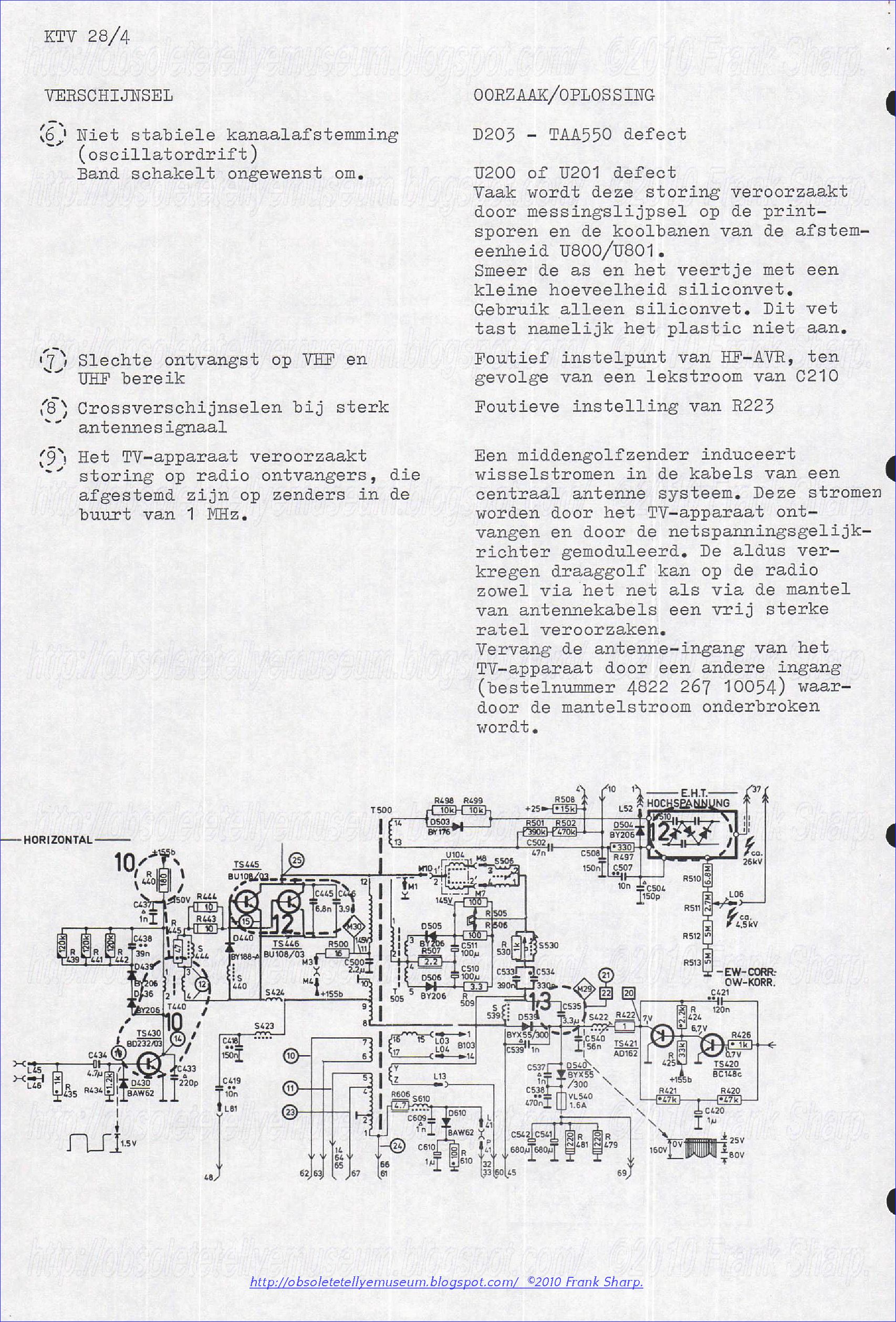


PHILIPS 26C465/58 CHASSIS K9 SWITCH MODE POWER SUPPLY CIRCUIT.


Control circuit for a switched-mode power supply, particularly for a television receiver: PHILIPS CHASSIS K9 SWITCH MODE POWER SUPPLY.
A switched-mode power supply provided with a control stage and a switching stage coupled by means of a transformer. The collector of an additional transistor is connected to the transformer. In this manner the ratio of the collector current to the base current of the switching transistor can assume a predetermined value, for example a constant value whatever the value of the mains voltage applied to the power supply.
It is known that the specific qualities of a switched-mode power supply depend for a large part on the switching speed of the switching transistor at the moment at which the latter passes periodically from the conductive state to the blocking state; this speed is at its maximum when the switching transistor presents, at the turn-off moment, a certain ratio between the collector current and the base current IC/IB: if this ratio is too low, the delay in the recombination of the charges stored in the base increases the switching time; if it is too high there is the risk that the transistor is brought out of saturation before it is blocked, which results in its substantially immediate destruction. For the known switched-mode power supplies it is not possible to maintain a suitable IC/IB ratio in the presence of large variations of the non-regulated rectified DC voltage which result from the connection to the nominal mains voltages of, for example, 110 or 220 V; actually, if the variations in IB are substantially proportional to the variations in the non-regulated voltage, the same does not happen for those of the IC whose amplitude is less.
CIRCUIT ARRANGEMENT FOR GENERATING IN A PICTURE DISPLAY DEVICE A SAWTOOTH CURRENT OF LINE FREQUENCY HAVING AN AMPLITUDE VARYING AT FIELD FREQUENCY IN PHILIPS CHASSIS K9.
A circuit arrangement for generating by means of a modulator in a colour picture display device a sawtooth correction current of line frequency flowing through the line deflection coils and having an amplitude varying at field frequency for the purpose of obtaining a better colour superposition in the corners of the screen of the display tube, comprising means to add an additional correction current which flows in the same direction as the first mentioned current and which is proportional to the third power of both the line and the field deflection currents. Said means may be a saturable coil or a resonant circuit which is tuned to a frequency which lies between the like frequency and twice the value thereof. In the latter case the voltage present across the circuit may be used for correcting the North-South pincushion distortion. Also, the modulator is controlled by an amplifier comprising a linear and a voltage-dependent resistor which ensure that a third-power component is added also to said field deflection current.
1. A distortion correction circuit for line and field deflection coils of a display tube, said circuit comprising line and field deflection generator means coupled to said coils respestively for producing line and field deflection signals respectively; a modulator means for providing a line frequency first correction current having a field frequency varying amplitude to at least one of said coils; and means for supplying an additional correction current distinct from said deflection signals that is a thrid power function of at least one of said deflection signals and for applying it to said one deflection coil in the same direction as said first correction current.
2. A circuit as claimed in claim 1 wherein said supplying means comprises a non-linear inductor series coupled to said modulator and having an inductance that decreases with increasing current.
3. A circuit as claimed in claim 1 wherein said supplying means comprises a tuned circuit including an inductor and a capacitor parallel coupled thereto, said circuit being tuned to a frequency between the line frequency and twice the line frequency and being series coupled to said modulator.
4. A circuit as claimed in claim 3 wherein said inductor comprises a transformer primary, said transformer including a secondary; and further comprising means coupled to said secondary for correcting North-South pincushion distortion in said display tube.
5. A circuit as claimed in claim 1 wherein said modulator comprises diode switch means operating at the line frequency for coupling during the line scan time the field generator to a resonant circuit having a period twice the line flyback period, said resonant circuit including a capacitor and said line deflection coil; and further comprising a coil coupled in series between said line generator and said line coil.
6. A circuit as claimed in claim 5 further comprising a resistor series coupled to said capacitor.
7. A circuit as claimed in claim 5 further comprising a series circuit including in order a first capacitor, a pair of diodes that are non-conducting during the line flyback time, and a second capacitor, said series circuit being parallel coupled to said coil; and an inductance capacitance parallel resonant circuit coupled to the junction of the diodes, said circuit being resonant at a frequency between the line frequency and twice the line frequency.
8. A circuit as claimed in claim 1 further comprising amplifier means for applying said field signal to said modulator, said amplifier including a complementary pair of transistors adapted to receive a negative feedback network having an input coupled to the output electrodes of said transistors for receiving a zero average signal, said network comprising fixed and voltage dependent resistors coupled thereto.
9. A circuit as claimed in claim 1 further comprising a circuit coupled between said modulator and said field generator, said circuit comprising a fixed and a voltage dependent resistor parallel coupled thereto.
10. A circuit as claimed in claim 1 further comprising North-South pincushion correction means for adding a sinusoidal current of line frequency to said correction current.
11. A circuit as claimed 1 wherein said additional correction current is a third power function of both of said deflection signals.
 Description:

1. A circuit for generating an output deflection current for a deflection coil from an input sawtooth deflection voltage signal having a polarity changes at the start of the flyback period which are short with respect to said flyback period; said circuit comprising an amplifier having an input adapted to receive said input signal, and an output means adapted to be coupled to said coil for providing said output current; means coupled to said amplifier for generating a control voltage that is the difference between a voltage that is proportional to said input signal and a voltage that is proportional to said output current; a direct voltage source; and means for rendering said output current independent of voltage and load variations comprising means for reversing the polarity of said deflection current at the start of said flyback period including a switch means coupled to said amplifier and said source and having a control input coupled to said means for generating for coupling said coil to said source at the start of said flyback period and separating said coil from said source upon said deflection current reaching a selected value required for the start of the scan period.
2. A circuit as claimed in claim 1, wherein said amplifier comprises a junction having a potential that differs from a threshold value during said flyback period, said switch being coupled to said junction and switching at about said threshold value; and further comprising feedback means for applying said voltage proportional to said deflection current to said amplifier input.
3. A circuit as claimed in claim 2 wherein said junction potential goes below said threshold value during said flyback period, said switch switching above said threshold value.
4. A circuit as claimed in claim 2 wherein said junction potential exceeds said threshold value during said flyback period, said switch switching below said threshold value.
5. A circuit as claimed in claim 2 wherein said amplifier comprises first and second final stage class B push pull transistors, each of said transistors having emitter and collector conduction electrodes, a conduction electrode of one of said transistors being coupled to a like conduction electrode of said other transistor, said first transistor being conductive during said start of said scan period; a pass direction coupled diode having a first end coupled to first transistor conduction electrode, and a second end adapted to receive a first terminal of a power supply; a capacitor having a first end coupled to said diode first end, and a second end coupled to said switch; and a resistor having a first end coupled to said capacitor second end, and a second end adapted to receive a second terminal of said power supply.
6. A circuit as claimed in claim 5 wherein said like conduction electrodes comprise said collector electrodes and said diode first end is coupled to said first transistor emitter.
7. A circuit as claimed in claim 5 wherein said like conduction electrodes comprise said emitter electrodes and said diode first end is coupled to said first transistor collector.
8. A circuit as claimed in claim 5 further comprising a second cut off direction coupled diode having a first end coupled to a conduction electrode of said first transistor, and a second end coupled to the remaining conduction electrode of said first transistor.
PHILIPS 26C465/58 CHASSIS K9 E/W CORRECTION Circuit arrangement in an image display apparatus for (horizontal) line deflection
Line deflection circuit in which the deflection coil is east-west modulated. In order to cancel an east-west dependent horizontal linearity defect the inductance value of the linearity correction coil is made independent of the field frequency, for example by means of a compensating current. In an embodiment this current is supplied by the shunt coil of the east-west modulator.
1. Circuit arrang ement for use with a line deflection coil, said circuit comprising a generator means adapted to be coupled to said coil for producing a sawtooth line-deflection current through said line deflection coil, said deflection current having a field-frequency component current, a horizontal linearity correction coil adapted to be coupled in series with said deflection coil and including an inductor having a bias-magnetized core, and means for making the inductance value of the linearity correction coil substantially independent of the field frequency component current. 2. Circuit arrangement as claimed in claim 1, wherein said making means includes a current supply source means for producing a compensating line-frequency sawtooth current through a winding of the linearity correction coil, the amplitude of the compensating current having a field-frequency variation. 3. Circuit arrangement as claimed in claim 2, wherein the direction of curvature of the field-frequency envelope of the compensating current is opposite to the direction of curvature of the field-frequency component current of the line deflection current, whereby the magnetic fields produced in the core of the correction coil by the two currents have the same direction. 4. Circuit arrangement as claimed in claim 2, wherein the direction of curvature of the field-frequency envelope of the compensating current is the same as the direction of curvature of the field-frequency component current of the line deflection current, whereby the magnetic fields produced in the core of the correction coil by the two currents have opposite directions. 5. Circuit arrangement as claimed in claim 2, wherein said correction coil further comprises an additional winding disposed on the core, said additional winding being coupled to said supply source means to receive the compensating current. 6. Circuit arrangement as claimed in claim 5, further comprising modulator means for modulating the line deflection current with said field frequency component, said modulator including a compensation coil coupled in series with said additional winding. 7. Horizontal linearity correction coil comprising a core made of a magnetic material and bias-magnetized by at least one permanent magnet, and an additional winding disposed on the core. 8. Image display apparatus including a circuit arrangement as claimed in claim 1.
PHILIPS 26C465/58 CHASSIS K9 Receiver tuning circuit PHILIPS CHASSIS K9
A receiver tuning circuit in which without operation of extra switches a change-over can be made from tuning by means of a continuously varying tuning voltage to tuning by means of one of a number of adjusted tuning voltages by using a capacitor controlled by an automatic tuning correction current source circuit for obtaining said voltage, and an automatic switch for applying the desired tuning voltages to this capacitor.
2. A receiver tuning circuit as claimed in claim 1, wherein said switch comprises a current source which can be influenced by an operating signal, said source being coupled to two parallel branches the first of which includes a transistor having an emitter coupled to said current source, a base coupled to an input of the switch, and a collector, a current mirror circuit having an input coupled to said collector and an output, the second branch including a pair of series connected diodes coupled to the current source and to said output of the current mirror circuit, and output of the switch being coupled to the pair of diodes.
3. A circuit as claimed in claim 1, further comprising a manually operable second switch means for obtaining a continuous coupling between said potentiometer means and said capacitor.
4. A circuit as claimed in claim 1 further comprising a supply circuit means for obtaining a desired tuning voltage, said memory means being independent of said supply circuit, said first switch further comprising a second time constant circuit means coupled to said supply circuit means for temporarily applying a tuning voltage determined by the potentiometer to said capacitor when the supply voltage is switched on.
5. A receiver tuning circuit comprising a tuning section having a tuning input, a capacitor means coupled to said tuning input for applying a tuning voltage thereto, a controllable current source coupled to said capacitor, a tuning correction signal detector means coupled between said tuning section and said current source for applying an automatic tuning correction signal to said capacitor through said current source, means coupled to said capacitor for immediately tuning said tuning section to a selected frequency independently of the previous voltage on said capacitor, a memory means coupled to said immediate tuning means for storing a tuning voltage corresponding to a selected frequency and signal amplitude detector means coupled to said immediate tuning means for effecting that said tuning voltage stored in said memory means is applied to said capacitor through said immediate tuning means when said signal amplitude goes below a selected value.

Circuit arrangement for establishing a reference potential of a chassis of an electrical device such as a radio and/or TV receiver, such device being provided with at least one contactless touching switch operating under the AC voltage principle. The device is switched by touching a unipole touching field in a contactless manner so as to establish connection to a grounded network pole. The circuit arrangement includes in combination an electronic blocking switch and a unidirectional rectifier which separates such switch from the network during the blocking phase.
 1. A circuit arrangement for establishing, at the chassis of an electrical device powered by a grounded AC supply network, a reference potential with relation to ground, said device having at least one contactless touching switch operating on the AC voltage principle, the switch being operated by touching a unipole touching field in a contactless manner, said arrangement comprising an electronic switch for selectively blocking the circuit of the device from the supply network, a half-wave rectifier including a pair of diodes individually connected in series-aiding relation between the terminals of the supply network and the terminals of the device for separating the electronic blocking switch from the supply network during a blocking phase defined by a prescribed half period of the AC cycle, and a pair of condensers individually connected in parallel with the respective diodes. 2. A circuit arrangement according to claim 1, wherein the capacitances of the two condensers are of equal magnitude.


Control circuit for a switched-mode power supply, particularly for a television receiver: PHILIPS CHASSIS K9 SWITCH MODE POWER SUPPLY.
A switched-mode power supply provided with a control stage and a switching stage coupled by means of a transformer. The collector of an additional transistor is connected to the transformer. In this manner the ratio of the collector current to the base current of the switching transistor can assume a predetermined value, for example a constant value whatever the value of the mains voltage applied to the power supply.
What is claimed is:
1. A control circuit for a switched-mode power supply, said power supply comprising a non-regulated rectified DC voltage source, a driver transistor, a first transformer having primary and secondary windings, an end of said primary being coupled to the collector-emitter path of said driver transistor, a switching transistor having a base coupled to said secondary, a second transformer having a primary winding coupled in series with said switching transistor, and a plurality of secondary windings, said control circuit comprising a first additional transistor having a collector coupled to the remaining end of the primary winding of the first transformer not connected to the driver-transistor and an emitter coupled to the non-regulated direct voltage source.
2. A control circuit as claimed in claim 1, further comprising a constant voltage source coupled to the base of the additional transistor.
3. A control circuit as claimed in claim 1, further comprising a constant current source, and a resistor coupled between the emitter of the additional transistor and the constant current source.
4. A control circuit as claimed in claim 3, wherein the constant current source comprises a second additional transistor, the two additional transistors being of complementary conductivity and their emitters being connected with each other through said resistor, the collector of the second additional transistor being coupled to the non-regulated rectified direct voltage source and the collector of the first additional transistor being coupled to the end of the primary winding of the first transformer not connected to the driver transistor.
5. A control circuit as claimed in claim 4, further comprising a resistor coupled in series with the collector circuit of said second additional transistor and the non-regulated rectified direct voltage source.
6. A control circuit as claimed in claim 5, further comprising a zener diode coupled between the base of the second additional transistor and the non-regulated voltage source.
7. A control circuit as claimed in claim 6, further comprising a resistance bridge coupled to the base of the first additional transistor and arranged between the two electrodes of the zener diode.
8. A control circuit as claimed in claim 7, wherein the driver transistor and the switching transistor do not conduct simultaneously, and the voltage between the two electrodes of the zener diode as well as the values of the resistors arranged between the said electrodes and of the resistor arranged between the emitters of the two additional transistors are chosen so that the first additional transistor is in the saturated state at the lowest value of the non-regulated voltage while it operates in the linear state at a higher value of said non-regulated voltage.
1. A control circuit for a switched-mode power supply, said power supply comprising a non-regulated rectified DC voltage source, a driver transistor, a first transformer having primary and secondary windings, an end of said primary being coupled to the collector-emitter path of said driver transistor, a switching transistor having a base coupled to said secondary, a second transformer having a primary winding coupled in series with said switching transistor, and a plurality of secondary windings, said control circuit comprising a first additional transistor having a collector coupled to the remaining end of the primary winding of the first transformer not connected to the driver-transistor and an emitter coupled to the non-regulated direct voltage source.
2. A control circuit as claimed in claim 1, further comprising a constant voltage source coupled to the base of the additional transistor.3. A control circuit as claimed in claim 1, further comprising a constant current source, and a resistor coupled between the emitter of the additional transistor and the constant current source.
4. A control circuit as claimed in claim 3, wherein the constant current source comprises a second additional transistor, the two additional transistors being of complementary conductivity and their emitters being connected with each other through said resistor, the collector of the second additional transistor being coupled to the non-regulated rectified direct voltage source and the collector of the first additional transistor being coupled to the end of the primary winding of the first transformer not connected to the driver transistor.
5. A control circuit as claimed in claim 4, further comprising a resistor coupled in series with the collector circuit of said second additional transistor and the non-regulated rectified direct voltage source.
6. A control circuit as claimed in claim 5, further comprising a zener diode coupled between the base of the second additional transistor and the non-regulated voltage source.7. A control circuit as claimed in claim 6, further comprising a resistance bridge coupled to the base of the first additional transistor and arranged between the two electrodes of the zener diode.
8. A control circuit as claimed in claim 7, wherein the driver transistor and the switching transistor do not conduct simultaneously, and the voltage between the two electrodes of the zener diode as well as the values of the resistors arranged between the said electrodes and of the resistor arranged between the emitters of the two additional transistors are chosen so that the first additional transistor is in the saturated state at the lowest value of the non-regulated voltage while it operates in the linear state at a higher value of said non-regulated voltage.
Description:
The present invention relates to a control circuit for a switched-mode power supply, particularly in a television receiver, said power supply comprising a rectified, non-regulated rectified DC voltage source, a driver transistor whose collector-emitter path is arranged in series with a primary winding of a first transformer, a secondary winding of the latter being coupled to the base of a switching transistor which is arranged in series with a primary winding of a second transformer having a plurality of secondary windings.
This type of switched-mode power supply is used more and more because of the numerous advantages it presents as regards energy efficiency, reliability, compactness, etc. However, as for the majority of the other types of power supplies, its operation on mains supplies of different voltages imposes the use of either a transformer with taps or switch-over from full wave rectification at the highest mains voltage to a voltage doubler rectification for the lowest mains voltage.
It is known that the specific qualities of a switched-mode power supply depend for a large part on the switching speed of the switching transistor at the moment at which the latter passes periodically from the conductive state to the blocking state; this speed is at its maximum when the switching transistor presents, at the turn-off moment, a certain ratio between the collector current and the base current IC/IB: if this ratio is too low, the delay in the recombination of the charges stored in the base increases the switching time; if it is too high there is the risk that the transistor is brought out of saturation before it is blocked, which results in its substantially immediate destruction. For the known switched-mode power supplies it is not possible to maintain a suitable IC/IB ratio in the presence of large variations of the non-regulated rectified DC voltage which result from the connection to the nominal mains voltages of, for example, 110 or 220 V; actually, if the variations in IB are substantially proportional to the variations in the non-regulated voltage, the same does not happen for those of the IC whose amplitude is less.
However, the importance of having a power supply which can operate without any switching on mains supplies of 110 or 220 V is evident: for the manufacturer it is cheaper to produce and the reliability is increased; while the user does not run the risk of incorrect manipulations, particularly when the power supply is destined for use in portable television sets.
One of the objects of the invention is to realize a control circuit which permits the switched-mode power supply to operate without switching in conditions which are substantially optimum and in the presence of mains voltage variations in the range of 90 to 250 Volts.
A further object of the invention is to ensure that said IC/IB ratio of the switching transistor has a predetermined and, more particularly a constant value at the turn-off moment whatever the value of the mains voltage applied to the power supply.
The control circuit according to the invention is characterized in that the end of the primary winding of the first transformer not connected to the driver transistor is connected to the collector of an additional transistor whose emitter is coupled with the non-regulated direct voltage source. Advantageously it is characterized in that the emitter of the additional transistor is connected to one end of a resistor, the other end of this resistor being connected to a constant current source, and that the constant current source is constituted by a second additional transistor, the two additional transistors being of complementary conductivity and their emitters being connected with each other through a resistor, whilst the collector of the second additional transistor is connected to one of the poles of the non-regulated rectified direct voltage source and the collector of the first additional transistor is connected to the end of the primary winding of the first transformer not connected to the driver transistor.
Whilst combining the action of a ballast transistor with that of a variable current generator, the circuit according to the invention thus maintains automatically a desired IC/IB ratio of the switching transistor whatever the value of the mains voltage applied to the power supply.
CIRCUIT ARRANGEMENT FOR GENERATING IN A PICTURE DISPLAY DEVICE A SAWTOOTH CURRENT OF LINE FREQUENCY HAVING AN AMPLITUDE VARYING AT FIELD FREQUENCY IN PHILIPS CHASSIS K9.
A circuit arrangement for generating by means of a modulator in a colour picture display device a sawtooth correction current of line frequency flowing through the line deflection coils and having an amplitude varying at field frequency for the purpose of obtaining a better colour superposition in the corners of the screen of the display tube, comprising means to add an additional correction current which flows in the same direction as the first mentioned current and which is proportional to the third power of both the line and the field deflection currents. Said means may be a saturable coil or a resonant circuit which is tuned to a frequency which lies between the like frequency and twice the value thereof. In the latter case the voltage present across the circuit may be used for correcting the North-South pincushion distortion. Also, the modulator is controlled by an amplifier comprising a linear and a voltage-dependent resistor which ensure that a
third-power component is added also to said field deflection current.1. A distortion correction circuit for line and field deflection coils of a display tube, said circuit comprising line and field deflection generator means coupled to said coils respestively for producing line and field deflection signals respectively; a modulator means for providing a line frequency first correction current having a field frequency varying amplitude to at least one of said coils; and means for supplying an additional correction current distinct from said deflection signals that is a thrid power function of at least one of said deflection signals and for applying it to said one deflection coil in the same direction as said first correction current.
2. A circuit as claimed in claim 1 wherein said supplying means comprises a non-linear inductor series coupled to said modulator and having an inductance that decreases with increasing current.
3. A circuit as claimed in claim 1 wherein said supplying means comprises a tuned circuit including an inductor and a capacitor parallel coupled thereto, said circuit being tuned to a frequency between the line frequency and twice the line frequency and being series coupled to said modulator.
4. A circuit as claimed in claim 3 wherein said inductor comprises a transformer primary, said transformer including a secondary; and further comprising means coupled to said secondary for correcting North-South pincushion distortion in said display tube.
5. A circuit as claimed in claim 1 wherein said modulator comprises diode switch means operating at the line frequency for coupling during the line scan time the field generator to a resonant circuit having a period twice the line flyback period, said resonant circuit including a capacitor and said line deflection coil; and further comprising a coil coupled in series between said line generator and said line coil.
6. A circuit as claimed in claim 5 further comprising a resistor series coupled to said capacitor.
7. A circuit as claimed in claim 5 further comprising a series circuit including in order a first capacitor, a pair of diodes that are non-conducting during the line flyback time, and a second capacitor, said series circuit being parallel coupled to said coil; and an inductance capacitance parallel resonant circuit coupled to the junction of the diodes, said circuit being resonant at a frequency between the line frequency and twice the line frequency.
8. A circuit as claimed in claim 1 further comprising amplifier means for applying said field signal to said modulator, said amplifier including a complementary pair of transistors adapted to receive a negative feedback network having an input coupled to the output electrodes of said transistors for receiving a zero average signal, said network comprising fixed and voltage dependent resistors coupled thereto.
9. A circuit as claimed in claim 1 further comprising a circuit coupled between said modulator and said field generator, said circuit comprising a fixed and a voltage dependent resistor parallel coupled thereto.
10. A circuit as claimed in claim 1 further comprising North-South pincushion correction means for adding a sinusoidal current of line frequency to said correction current.
11. A circuit as claimed 1 wherein said additional correction current is a third power function of both of said deflection signals.
Description:
The invention relates to a circuit arrangement for generating in a picture display device a sawtooth correction current of line frequency having an amplitude varying at field frequency, the picture display device being provided with a line and a field deflection current generator for applying a sawtooth current of line and field frequency to a line and a field deflection coil at a substantially constant peak-to-peak amplitude, and a modulator controlled by the field deflection generator for obtaining the amplitude variation of field frequency of the sawtooth correction current of line frequency, said sawtooth correction current of line frequency being proportional to the instantaneous value of the line deflection current and of the field deflection current.
U.S. Pat. No. 3,440,483 described a display device for colour television wherein for the purpose of correction on the screen of a display tube in the device use is made of a sawtooth correction current of line frequency having an amplitude varying at field frequency. From the beginning up to the end of the scan of a field period this correction current of line frequency is to decrease down to zero from a given value in a substantially linear manner, whereafter a substantially equal increase in the reverse current direction follows. This correction current is superimposed on the deflection current flowing in the line and/or field deflection coil, the peak-to-peak a mplitude of the deflection current being substantially constant. Since the deflection coil is divided into two coil halves provided substantially symmetrically on either side of the neck of the display tube, it is possible to add the correction current in one coil half to the deflection current and to subtract it from the deflection current in the other coil half. The magnetic deflection field of one coil half will therefore be enlarged and that of the other coil half will be reduced to a substantially equal extent.
As has been described in the said U.S. patent the so-called anisotropic astigmatism of a deflection coil causes a distortion which gives an electron beam having a circular or ellipse cross-section a tilted ellipse shape, which distortion is dependent on the extent of the deflection. In other words, this distortion occurs most seriously in the corners of the displayed picture and it results in colour superposition errors. The said patent application shows that it is possible to eliminate this distortion with the aid of an oppositely directed distortion caused by the above-mentioned correction current.
The said amplitude variation of field frequency of the sawtooth current of line frequency is established by means of a modulator controlled by the field deflection current generator. The said patent application describes inter alia an arrangement wherein this modulator is formed as a multiplier to which information regarding the line and field deflection currents is supplied. If the centre horizontal line on the screen of the display tube is referred to as x'Ox and the central vertical line is referred to as y'Oy, wherein O is the centre of the screen while, as is common practice in mathematics, x'Ox extends from left to right y'Oy extends from bottom to top, it can be assumed that the compensating deviation Δ x which is established by means of the modulator is in the first instance proportional to x and to y. In this case x and y are the coordinates of one point on the screen relative to the previously defined system of coordinates. In this manner the compensating deviation Δ x is indeed increased in the corners of the screen and is zero on the axes x'Ox and y'Oy.
However, the invention is based on the recognition of the fact that the previously described correction is not sufficient to completely eliminate the colour superposition errors in the corners of the screen of the display tube. In order to be able to eliminate this the circuit arrangement according to the invention is characterized in that it includes means to add an additional correction current to the sawtooth current in the vicinity of the beginning and the end of each scan period, which additional current flows in the same direction as the said correction current and which is proportional to the third power of the line deflection current and to the third power of the field deflection current.
The correction currents may be produced in different manners. To this end the circuit arrangement according to the invention is further characterized in that the means for producing the additional correction current during the line scan period are obtained by means of a coil which is series-arranged with the modulator and whose inductance decreases when the current flowing therethrough increases and that the means for producing the additional correction current during the line scan period are obtained by means of a parallel circuit which is series-arranged with the modulator and whose resonant frequency lies between the line frequency and twice the value thereof.
Furthermore the invention is based on the recognition of the fact that the voltage which is present under these circumstances across the said parallel circuit may alternatively be used for other purposes. To this end, the circuit arrangement according to the invention is characterized in that the coil in the parallel circuit constitutes the primary winding of a transformer and that the voltage produced across the secondary winding of the transformer controls a circuit for the correction of the North-South pincushion distortion on the screen of a picture display tube present in the picture display device.
U.S. Pat. No. 3,440,483 described a display device for colour television wherein for the purpose of correction on the screen of a display tube in the device use is made of a sawtooth correction current of line frequency having an amplitude varying at field frequency. From the beginning up to the end of the scan of a field period this correction current of line frequency is to decrease down to zero from a given value in a substantially linear manner, whereafter a substantially equal increase in the reverse current direction follows. This correction current is superimposed on the deflection current flowing in the line and/or field deflection coil, the peak-to-peak a
mplitude of the deflection current being substantially constant. Since the deflection coil is divided into two coil halves provided substantially symmetrically on either side of the neck of the display tube, it is possible to add the correction current in one coil half to the deflection current and to subtract it from the deflection current in the other coil half. The magnetic deflection field of one coil half will therefore be enlarged and that of the other coil half will be reduced to a substantially equal extent.As has been described in the said U.S. patent the so-called anisotropic astigmatism of a deflection coil causes a distortion which gives an electron beam having a circular or ellipse cross-section a tilted ellipse shape, which distortion is dependent on the extent of the deflection. In other words, this distortion occurs most seriously in the corners of the displayed picture and it results in colour superposition errors. The said patent application shows that it is possible to eliminate this distortion with the aid of an oppositely directed distortion caused by the above-mentioned correction current.
The said amplitude variation of field frequency of the sawtooth current of line frequency is established by means of a modulator controlled by the field deflection current generator. The said patent application describes inter alia an arrangement wherein this modulator is formed as a multiplier to which information regarding the line and field deflection currents is supplied. If the centre horizontal line on the screen of the display tube is referred to as x'Ox and the central vertical line is referred to as y'Oy, wherein O is the centre of the screen while, as is common practice in mathematics, x'Ox extends from left to right y'Oy extends from bottom to top, it can be assumed that the compensating deviation Δ x which is established by means of the modulator is in the first instance proportional to x and to y. In this case x and y are the coordinates of one point on the screen relative to the previously defined system of coordinates. In this manner the compensating deviation Δ x is indeed increased in the corners of the screen and is zero on the axes x'Ox and y'Oy.
However, the invention is based on the recognition of the fact that the previously described correction is not sufficient to completely eliminate the colour superposition errors in the corners of the screen of the display tube. In order to be able to eliminate this the circuit arrangement according to the invention is characterized in that it includes means to add an additional correction current to the sawtooth current in the vicinity of the beginning and the end of each scan period, which additional current flows in the same direction as the said correction current and which is proportional to the third power of the line deflection current and to the third power of the field deflection current.
The correction currents may be produced in different manners. To this end the circuit arrangement according to the invention is further characterized in that the means for producing the additional correction current during the line scan period are obtained by means of a coil which is series-arranged with the modulator and whose inductance decreases when the current flowing therethrough increases and that the means for producing the additional correction current during the line scan period are obtained by means of a parallel circuit which is series-arranged with the modulator and whose resonant frequency lies between the line frequency and twice the value thereof.
Furthermore the invention is based on the recognition of the fact that the voltage which is present under these circumstances across the said parallel circuit may alternatively be used for other purposes. To this end, the circuit arrangement according to the invention is characterized in that the coil in the parallel circuit constitutes the primary winding of a transformer and that the voltage produced across the secondary winding of the transformer controls a circuit for the correction of the North-South pincushion distortion on the screen of a picture display tube present in the picture display device.
FRAME DEFLECTION CIRCUIT CHASSIS K9
A field deflection circuit in which the deflection coil is connected to a direct voltage source during the flyback period so as to reverse the polarity of the deflection current. For this purpose the deflection coil is connected through a switch controllable connected to the direct voltage source, which switch is controlled by the difference between a voltage proportional to the steep-edged sawtooth input signal and a voltage proportional to the deflection current. This difference is considerable during the flyback period and is utilized for switching on the controllable switch; it becomes zero as soon as the deflection current has reached its required value at which the switch is switched off again. It is thus achieved that the polarity reversal is always terminated when the required value is reached, even when the direct voltage fluctuates and also when the inductive load is changed.

1. A circuit for generating an output deflection current for a deflection coil from an input sawtooth deflection voltage signal having a polarity changes at the start of the flyback period which are short with respect to said flyback period; said circuit comprising an amplifier having an input adapted to receive said input signal, and an output means adapted to be coupled to said coil for providing said output current; means coupled to said amplifier for generating a control voltage that is the difference between a voltage that is proportional to said input signal and a voltage that is proportional to said output current; a direct voltage source; and means for rendering said output current independent of voltage and load variations comprising means for reversing the polarity of said deflection current at the start of said flyback period including a switch means coupled to said amplifier and said source and having a control input coupled to said means for generating for coupling said coil to said source at the start of said flyback period and separating said coil from said source upon said deflection current reaching a selected value required for the start of the scan period.
2. A circuit as claimed in claim 1, wherein said amplifier comprises a junction having a potential that differs from a threshold value during said flyback period, said switch being coupled to said junction and switching at about said threshold value; and further comprising feedback means for applying said voltage proportional to said deflection current to said amplifier input.
3. A circuit as claimed in claim 2 wherein said junction potential goes below said threshold value during said flyback period, said switch switching above said threshold value.
4. A circuit as claimed in claim 2 wherein said junction potential exceeds said threshold value during said flyback period, said switch switching below said threshold value.
5. A circuit as claimed in claim 2 wherein said amplifier comprises first and second final stage class B push pull transistors, each of said transistors having emitter and collector conduction electrodes, a conduction electrode of one of said transistors being coupled to a like conduction electrode of said other transistor, said first transistor being conductive during said start of said scan period; a pass direction coupled diode having a first end coupled to first transistor conduction electrode, and a second end adapted to receive a first terminal of a power supply; a capacitor having a first end coupled to said diode first end, and a second end coupled to said switch; and a resistor having a first end coupled to said capacitor second end, and a second end adapted to receive a second terminal of said power supply.
6. A circuit as claimed in claim 5 wherein said like conduction electrodes comprise said collector electrodes and said diode first end is coupled to said first transistor emitter.
7. A circuit as claimed in claim 5 wherein said like conduction electrodes comprise said emitter electrodes and said diode first end is coupled to said first transistor collector.
8. A circuit as claimed in claim 5 further comprising a second cut off direction coupled diode having a first end coupled to a conduction electrode of said first transistor, and a second end coupled to the remaining conduction electrode of said first transistor.
Description:
The invention relates to a field deflection circuit including an amplifier whose input conveys a saw-tooth signal whose polarity changes at the commencement of the flyback period within a period of time which is very short as compared with the flyback period, the field deflection coil being connected to the output of said amplifier, and a controllable switch by means of which the deflection coil is connected to a direct voltage source at the commencement of the flyback pulse for the purpose of reversing the polarity of the deflection current.
As compared with a vertical deflection circuit in which the deflection coil with an additionally arranged capacitor is constituted as a part of a resonance circuit, which circuit performs an unattenuated half oscillation during the flyback period whereby considerable voltage amplitudes at the output of the amplifier circuit occur, the advantage of such a deflection circuit is that the direct voltage to which the deflection coil must be connected is not so high, so that transistors having a slight collector breakdown voltage can be used. In a circuit arrangement of the kind described in the preamble and in U.S. Pat. No. 3,070,727 the flyback voltage depends on the height of the direct voltage, the inductance of the deflection coil and the maximum deflection current in accordance with the relation T = LI/U, in which T denotes the duration of the polarity reversal, I denotes the height of the deflection current (measured from peak to peak), L denotes the inductance of the deflection coil and U denotes the height of the direct voltage.
In a known circuit arrangement of this kind the input of the controllable (transistor) switch is connected to the output of theamplifier through the series arrangement of a capacitor and a resistor. At the commencement of the flyback period the sawtooth voltage changes from its positive to its negative maximum value while a negative pulse becomes available through the RC member at the input of the transistor switch, which pulse causes this transistor to conduct and which connects the deflection coil to a negative direct voltage so that the current flowing through the coil is reversed in polarity. The duration of this polarity reversal depends on the time constant of the RC member before the input of the transistor switch. In case of fluctuations of the direct voltage to which the deflection coil is connected during the flyback period, the amplitude of the current reached by the deflection current during this polarity reversal of course also changes so that the scan period commences either at a too low or at a too high value of the vertical deflection current. Since in addition, as stated, the period of time during which the deflection coil must be connected to the direct voltage depends on the inductance of the deflection coil, the time constant of the RC member must be adapted to the inductance of the deflection coils.
An object of the present invention is to obviate these drawbacks and to provide a circuit arrangement in which the deflection coil is connected to the direct voltage as long as is necessary for reaching the amplitude of the deflection current required for the commencement of the scan period and in which an adaptation is not necessary when the inductance of the deflection circuit changes, for example, by including a transformer for the North-South raster correction.
Starting from a vertical deflection circuit of the kind described in the preamble this object is achieved according to the invention in that the controllable switch is controlled by the difference between a voltage which is proportional to the sawtooth signal and a voltage which is proportional to the deflection current, said two voltages and/or the switch being dimensioned in such a manner that the deflection coil is separated from the direct voltage by means of the switch as soon as the current flowing through the deflection coil has reached the value required for the commencement of the scan period.
The invention is based on the regulation of the fact that the sawtooth signal at the input of the amplifier and the current flowing through the vertical deflection coil have substantially the same variation throughout the scan period; during the flyback period the sawtooth signal is, however, reversed in polarity within a few microseconds, while the polarity reversal for the deflection current is considerably slower due to the limited direct voltage present at the deflection coil. These differences in the variation with time between the input signal and the deflection current may be utilized for the purpose of rendering the switch operative, which switch becomes inoperative again as soon as the deflection current has reached its value required for the commencement of the scan period, because then no difference exists any longer between the sawtooth input signal and the deflection current.
According to a further embodiment of the invention the voltage proportional to the deflection current is applied as a feedback voltage to the input of the amplifier and the controllable switch is connected to a point of the amplifier whose potential exceeds a threshold value only during the flyback period, which threshold value renders the controllable switch operative.
In order that the invention may be readily carried into effect, an embodiment thereof will now be described in detail by way of example with reference to the accompanying diagrammatic drawing. In this embodiment a class B push-pull amplifier is used which, as is known, has a lower dissipation then a class A amplifier for a determined deflection output. The amplifier is substantially symmetrical so that two corresponding parts are denoted by two corresponding reference numerals (for example, 12, 12').
The input signal 1 is applied through a capacitor 2 of 10 μF to the interconnected bases of the input transistors 3 and 3'. The collector of npn-transistor 3 is connected through a resistor 4 of 1.5 kOhms to the positive supply voltage terminal, while its emitter is connected through a resistor 5 of 6.8 kOhms to the negative supply voltage. Transistor 3' is of the pnp type and accordingly it has a polarity which is opposite to that of transistor 3; however, the resistors 4' in the collector lead and 5' in the emitter lead have the same values as resistors 4 and 5. The collector of the transistor 3(3') is connected to the base of a pnp- (npn-) transistor 6 (6') whose emitter is connected through a resistor 7 (7') of 470 Ohms to the positive (negative) supply voltage. The collectors of transistors 6 and 6' are connected together through a diode arranged in the pass direction. The collector voltages of transistors 6 and 6' are applied to the bases of transistors 8 and 8' which are of a conductivity type opposite to that of the transistors driving them. The collectors of transistors 8 and 8' are connected through resistors 9 and 9' to the bases of final transistors 10 and 10' which are again of a conductivity type which is opposite to that of the transistors driving them. The collectors of transistors 10 and 10' are connected together and the junction is connected to ground through the deflection coil 11 and a low-value resistor 12 of 2.2 Ohms. The final transistors are protected by diodes 15 and 15' from the voltage peaks occurring at the deflection coil when the current is reversed in polarity and when flashovers occur in the picture display tube, said diodes being connected in the blocking direction in parallel with the collector-emitter path of the final transistors. In case of a short circuit at the end of the final stage the driver current is limited by the resistors 9, 9'.
In case of a class B push-pull stage the output potential is normally highly dependent on the adjusted quiescent current which in turn is determined by the ambient temperature. In the present circuit arrangement this would give rise to the fact that the vertical position of the picture highly depends on the temperature. To avoid this, the bases of the final transistors 10 and 10' are connected through the series arrangement of diodes 13 and 13' arranged in the pass direction and resistors 14 and 14' to supply voltage terminal for their emitters. A resistor 16 of 47 kOhms arranged between the cathode of the diode 13 connected to the positive potential and the anode of the diode 13' connected to the negative potential ensures that the diodes 13 and 13' are always slightly biassed. As a result the base potential and the quiescent current of the final transistors 10 and 10' is determined by the bias voltage of these diodes when the input signal fails, hence when transistors 8 and 8' are cut off. Since this bias voltage is already very low and is even more reduced by the voltage drops at resistors 14 and 14', quiescent currents of a few μA can be adjusted. The distortions of the output signal to be expected at such a low quiescent current adjustment are eliminated in known manner (Austrian Pat. specification 245038) in that the bases of the final transistors are not connected to the emitters of the driver stages 8 and 8' but to their collectors so that the output resistance of the driver stages 8, 8' driving the final transistors 10, 10' is considerably larger than the input resistance of the final stages. The non-linearity of the input resistance therefore does not exert any influence on the course of the signal.
A voltage is derived from resistor 12 which is applied through resistors 17 and 17' to the emitters of input transistors 3 and 3'. The voltage 18 proportional to the deflection current derived from resistor 12 has the same phase and substantially also the same shape as the input signal 1 and therefore acts as a direct current feedback. The mean value of the deflection current and hence the position of the picture is determined in this circuit arrangement by the potential at the bases of transistors 3 and 3'. To adjust this potential a potentiometer connected to the supply voltage would be sufficient, while its wiper would be connected to the bases of the input transistors, but in this case the position of the picture would be greatly dependent on fluctuations in the supply voltage. Adjustment of the picture position substantially independent of supply voltage fluctuations is obtained when, as shown in the drawing, the base is connected to the wiper on a potentiometer 18' of 5 kOhms whose ends are connected to ground through resistors 19 and 19' of 22 kOhms and further resistors 20 and 20' of 330 Ohms, the junction of resistors 19, 20 and 19', 20' being connected through resistors 21 and 21', respectively, to the positive and negative potential, respectively. The amplifier and particularly the driver stages 8, 8' and the final stages 10, 10' are substantially insensitive to hum voltages so that the positive voltage of 24 volts and the negative voltage of -20 Volts need not be especially smooth. For the preliminary stages this smoothing may be effected in known manner by resistors 22 and 22' of 680 Ohms arranged in the supply lead which resistors together with capacitors 23 and 23' of 500 μF constitute a smoothing member.
It is achieved by the direct current feedback that the deflection current is adjusted such that the voltage fed back on the emitters of the input transistors 3 and 3' corresponds but for a small difference to the voltage at the bases of transistor 3 and 3' (for this reason the deflection current can be varied by varying the value of resistor 12 in case of a given amplitude of the input signal). As a result the deflection current has the same variation with time as the input signal 1 at least during the scan period. At the beginning of the flyback period the input voltage changes within a few microseconds from its positive to its negative maximum value; the deflection current can, however, not be reversed in polarity at the same rate. As a result the base-emitter voltage of the input transistors 3 varies substantially stepwise after the beginning of the flyback period when the input signal has already reached its negative peak value while the deflection current has only very slightly varied. The bases of the input transistors 3, 3' become thus considerably more negative so that the lower transistor 3' and at the same time the transistors 6', 8', 10' conduct heavily while transistors, 3, 6, 8 and 10 are cut off. This voltage variation produces a negative voltage step, for example, at the interconnected emitters of driver transistor 8, 8' which emitters are connected to ground through a resistor 24 of 100 Ohms, said voltage step being applied to the input of a controllable switch 27 through a potential divider consisting of resistors 25 of 1 kOhm and 26 of 22 kOhms and having one end connected to the said emitters and the other end connected to the positive supply voltage, so that said switch then onducts. In the conducting state the switch 27 must conduct current in both directions; when using a transistors switch the collector-emitter path of the switching transistor may be connected for this purpose in parallel with a diode having an opposite pass direction and having such a polarity that it does not conduct during the scan period.
The current flowing through the deflection coil might alternatively be reversed in polarity when the deflection coil would be directly connected via the switch to the negative supply voltage. In case of a negative supply voltage of - 20 Volts, a deflection inductance of 30 mH and a deflection current of 1,2 A (peak-to-peak) a time of 1.8 ms would, however, be required for reversing the polarity of the deflection current; a flyback period of less than one ms is, however, desirable. This shorter flyback period could be obtained by increasing the negative and the positive supply voltage. Then, however, the dissipation of the final stage transistors 10, 10' would also be increased.
In the circuit arrangement shown in the drawing the duration of the flyback period is reduced by means of a clamping circuit without increase of dissipation of the final stage transistors. For this purpose the emitter of transistor 10', unlike the emitter of transistor 10 is not directly connected to the associated voltage supply terminal but through a diode 28 conducting in the pass direction. In addition the emitter of transistor 10' is connected through a large capacitor 29 of 250 μF to the end of the transistor switch not connected to the negative supply voltage, which end is simultaneously connected through a resistor 30 of 220 Ohms to the positive supply voltage terminal. The clamping circuit operates as follows:
During the scan period capacitor 29 is charged through resistor 30 and the diode 28, a voltage of + 24 Volts occurring at the end of capacitor 29 connected to the switch and a voltage of approximately - 20 Volts occurring at the other end, so that a voltage of approximately 44 Volts is present at the capacitor. As soon as the transistor switch 27 conducts as a result of the steep-edged voltage step of the input voltage 1 the electrode of capacitor 29 which was positive (+ 24 Volts) up till that instant is connected to the negative supply voltage; this potential step is transferred to the other electrode of the capacitor which was previously at - 20 Volts and subsequently at approximately - 60 Volts. Diode 28 is blocked at this voltage.
At the beginning of the flyback period a negative voltage peak is produced at the end of the deflection coil 11 connected to the amplifier output, and this as a result of the sudden cut-off of the final stage transistor 10 which was still conducting relatively strongly at the end of the scan period. The negative voltage peak is limited by diode 15' to a voltage which is slightly more negative than - 60 Volts, for example, -60.6 Volts. The deflection current flows via diode 15' in the same direction as it did previously through transistor 10, but due to the negative voltage at the end of the deflection coil connected to the amplifier output it decreases to the value of zero. Subsequently, the current is reversed in polarity and flows through the collector-emitter path of the npn transistor 10' whose base also carries a positive voltage during the first part of the flyback period. The voltage at the deflection coil is then only slightly less negative than the voltage on the left-hand electrode of capacitor 29 due to the small voltage drop on the collector-emitter path of transistor 10', so that the deflection current furthermore decreases at approximately the same rate as during the first half of the flyback period, because substantially the same voltage is present at the deflection coil. Simultaneously also the voltage at resistor 12 decreases and hence the difference between the base-emitter voltages of the input transistors 3 and 3'. Consequently the lower half of the class B push-pull amplifier becomes less conducting so that the emitter potential of transistors 8 and 8' becomes again less negative. In case of suitable dimensioning of the potential divider 25, 26 and of the threshold at which the transistor switch 27 is opened again it can be achieved that opening is effected just at the instant when the deflection current has reached its required value. The capacitor 29 is still further charged during the first part of the flyback period and the more the lower its capacitance is, and during the second part of the flyback period it is discharged to the voltage present at the commencement of the flyback period. The mean value of the potential on the left-hand electrode of this capacitor is thus still more negative than - 60 Volts during the flyback period and the more as the capacitance of the capacitor is lower so that the deflection current is reversed in polarity at an even faster rate. However, restrictions are imposed in this case due to the dielectric strength of the final stage transistors; consequently, when the dielectric strength of transistors 10, 10' is only slightly more than 60 Volts, a capacitor having a high capacitance (250 μF) is to be used, as in the embodiment.
This circuit arrangement is insensitive to fluctuations during operation. When, for example, the negative and/or the positive supply voltage increases, the flyback duration decreases; accordingly the emitter potential of the driver transistors 8 and 8' reaches the positive threshold value more quickly so that the switch is opened again and the polarity reversal is interrupted as soon as the deflection current has reached its required value.
PHILIPS 26C465/58 CHASSIS K9 NORD SOUTH (NORD/SUD) CORRECTION CIRCUIT ARRANGEMENT FOR CORRECTING THE DEFLECTION OF AT LEAST ONE ELECTRON BEAM IN A TELEVISION PICTURE TUBE BY MEANS OF A TRANSDUCTOR :
A circuit arrangement for raster correction in a television picture tube by means of a transductor whose power winding is connected in parallel with at least a portion of the line deflection coils, the line deflection genera tor having a low internal impedance. In order to increase this impedance a mainly inductive impedance is connected in series with the generator. In a picture tube employing at least two electron beams the series impedance may include the convergence circuit. As a result the convergence in the corners of the picture screen is also improved. The linearity control circuit may likewise form part of the series impedance.
1. A deflection circuit for a cathode ray tube comprising a transistor horizontal deflection generator; a horizontal deflection coil parallel coupled to said generator; means for pincushion correction of said tube comprising a saturable reactor having a control winding adapted to receive a vertical deflection signal and a power winding parallel coupled to at least a portion of said deflection coil; and means for increasing the effectiveness of said correction means comprising an impedance element external to said generator having a substantially inductive reactance series coupled between said generator and said coil. 2. A circuit as claimed in claim 1 wherein said generator comprises a transformer having a tap and said power winding has a first end coupled to said coil and a second end coupled to said tap. 3. A circuit as claimed in claim 1 wherein said impedance element comprises means for controlling the linearity of the beam deflection. 4. A deflection circuit for a cathode ray tube having at least two electron beams comprising a transistor horizontal deflection generator; a horizontal deflection coil parallel coupled to said generator; means for pincushion correction of said tube comprising a saturable reactor having a control winding adapted to receive a vertical deflection signal and a power winding parallel coupled to at least a portion of said deflection coil; means for increasing the effectiveness of said correction means comprising an Impedance element external to said generator having a substantially inductive reactance series coupled between said generator and said coil; and means for dynamically converging said beams comprising a convergence circuit coupled to said horizontal generator and to said transductor. 5. A circuit as claimed in claim 4 wherein said generator comprises a transformer having a tap and said power winding has a first end coupled to said coil and a second end coupled to said tap. 6. A circuit as claimed in claim 4 wherein said impedance element comprises means for controlling the linearity of the beam deflection.
As compared with a vertical deflection circuit in which the deflection coil with an additionally arranged capacitor is constituted as a part of a resonance circuit, which circuit performs an unattenuated half oscillation during the flyback period whereby considerable voltage amplitudes at the output of the amplifier circuit occur, the advantage of such a deflection circuit is that the direct voltage to which the deflection coil must be connected is not so high, so that transistors having a slight collector breakdown voltage can be used. In a circuit arrangement of the kind described in the preamble and in U.S. Pat. No. 3,070,727 the flyback voltage depends on the height of the direct voltage, the inductance of the deflection coil and the maximum deflection current in accordance with the relation T = LI/U, in which T denotes the duration of the polarity reversal, I denotes the height of the deflection current (measured from peak to peak), L denotes the inductance of the deflection coil and U denotes the height of the direct voltage.
In a known circuit arrangement of this kind the input of the controllable (transistor) switch is connected to the output of the
amplifier through the series arrangement of a capacitor and a resistor. At the commencement of the flyback period the sawtooth voltage changes from its positive to its negative maximum value while a negative pulse becomes available through the RC member at the input of the transistor switch, which pulse causes this transistor to conduct and which connects the deflection coil to a negative direct voltage so that the current flowing through the coil is reversed in polarity. The duration of this polarity reversal depends on the time constant of the RC member before the input of the transistor switch. In case of fluctuations of the direct voltage to which the deflection coil is connected during the flyback period, the amplitude of the current reached by the deflection current during this polarity reversal of course also changes so that the scan period commences either at a too low or at a too high value of the vertical deflection current. Since in addition, as stated, the period of time during which the deflection coil must be connected to the direct voltage depends on the inductance of the deflection coil, the time constant of the RC member must be adapted to the inductance of the deflection coils.An object of the present invention is to obviate these drawbacks and to provide a circuit arrangement in which the deflection coil is connected to the direct voltage as long as is necessary for reaching the amplitude of the deflection current required for the commencement of the scan period and in which an adaptation is not necessary when the inductance of the deflection circuit changes, for example, by including a transformer for the North-South raster correction.
Starting from a vertical deflection circuit of the kind described in the preamble this object is achieved according to the invention in that the controllable switch is controlled by the difference between a voltage which is proportional to the sawtooth signal and a voltage which is proportional to the deflection current, said two voltages and/or the switch being dimensioned in such a manner that the deflection coil is separated from the direct voltage by means of the switch as soon as the current flowing through the deflection coil has reached the value required for the commencement of the scan period.
The invention is based on the regulation of the fact that the sawtooth signal at the input of the amplifier and the current flowing through the vertical deflection coil have substantially the same variation throughout the scan period; during the flyback period the sawtooth signal is, however, reversed in polarity within a few microseconds, while the polarity reversal for the deflection current is considerably slower due to the limited direct voltage present at the deflection coil. These differences in the variation with time between the input signal and the deflection current may be utilized for the purpose of rendering the switch operative, which switch becomes inoperative again as soon as the deflection current has reached its value required for the commencement of the scan period, because then no difference exists any longer between the sawtooth input signal and the deflection current.
According to a further embodiment of the invention the voltage proportional to the deflection current is applied as a feedback voltage to the input of the amplifier and the controllable switch is connected to a point of the amplifier whose potential exceeds a threshold value only during the flyback period, which threshold value renders the controllable switch operative.
In order th
at the invention may be readily carried into effect, an embodiment thereof will now be described in detail by way of example with reference to the accompanying diagrammatic drawing. In this embodiment a class B push-pull amplifier is used which, as is known, has a lower dissipation then a class A amplifier for a determined deflection output. The amplifier is substantially symmetrical so that two corresponding parts are denoted by two corresponding reference numerals (for example, 12, 12').The input signal 1 is applied through a capacitor 2 of 10 μF to the interconnected bases of the input transistors 3 and 3'. The collector of npn-transistor 3 is connected through a resistor 4 of 1.5 kOhms to the positive supply voltage terminal, while its emitter is connected through a resistor 5 of 6.8 kOhms to the negative supply voltage. Transistor 3' is of the pnp type and accordingly it has a polarity which is opposite to that of transistor 3; however, the resistors 4' in the collector lead and 5' in the emitter lead have the same values as resistors 4 and 5. The collector of the transistor 3(3') is connected to the base of a pnp- (npn-) transistor 6 (6') whose emitter is connected through a resistor 7 (7') of 470 Ohms to the positive (negative) supply voltage. The collectors of transistors 6 and 6' are connected together through a diode arranged in the pass direction. The collector voltages of transistors 6 and 6' are applied to the bases of transistors 8 and 8' which are of a conductivity type opposite to that of the transistors driving them. The collectors of transistors 8 and 8' are connected through resistors 9 and 9' to the bases of final transistors 10 and 10' which are again of a conductivity type which is opposite to that of the transistors driving them. The collectors of transistors 10 and 10' are connected together and the junction is connected to ground through the deflection coil 11 and a low-value resistor 12 of 2.2 Ohms. The final transistors are protected by diodes 15 and 15' from the voltage peaks occurring at the deflection coil when the current is reversed in polarity and when flashovers occur in the picture display tube, said diodes being connected in the blocking direction in parallel with the collector-emitter path of the final transistors. In case of a short circuit at the end of the final stage the driver current is limited by the resistors 9, 9'.
In case of a class B push-pull stage the output potential is normally highly dependent on the adjusted quiescent current which in turn is determined by the ambient temperature. In the present circuit arrangement this would give rise to the fact that the vertical position of the picture highly depends on the temperature. To avoid this, the bases of the final transistors 10 and 10' are connected through the series arrangement of diodes 13 and 13' arranged in the pass direction and resistors 14 and 14' to supply voltage terminal for their emitters. A resistor 16 of 47 kOhms arranged between the cathode of the diode 13 connected to the positive potential and the anode of the diode 13' connected to the negative potential ensures that the diodes 13 and 13' are always slightly biassed. As a result the base potential and the quiescent current of the final transistors 10 and 10' is determined by the bias voltage of these diodes when the input signal fails, hence when transistors 8 and 8' are cut off. Since this bias voltage is already very low and is even more reduced by the voltage drops at resistors 14 and 14', quiescent currents of a few μA can be adjusted. The distortions of the output signal to be expected at such a low quiescent current adjustment are eliminated in known manner (Austrian Pat. specification 245038) in that the bases of the final transistors are not connected to the emitters of the driver stages 8 and 8' but to their collectors so that the output resistance of the driver stages 8, 8' driving the final transistors 10, 10' is considerably larger than the input resistance of the final stages. The non-linearity of the input resistance therefore does not exert any influence on the course of the signal.
A voltage is derived from resistor 12 which is applied through resistors 17 and 17' to the emitters of input transistors 3 and 3'. The voltage 18 proportional to the deflection current derived from resistor 12 has the same phase and substantially also the same shape as the input signal 1 and therefore acts as a direct current feedback. The mean value of the deflection current and hence the position of the picture is determined in this circuit arrangement by the potential at the bases of transistors 3 and 3'. To adjust this potential a potentiometer connected to the supply voltage would be sufficient, while its wiper would be connected to the bases of the input transistors, but in this case the position of the picture would be greatly dependent on fluctuations in the supply voltage. Adjustment of the picture position substantially independent of supply voltage fluctuations is obtained when, as shown in the drawing, the base is connected to the wiper on a potentiometer 18' of 5 kOhms whose ends are connected to ground through resistors 19 and 19' of 22 kOhms and further resistors 20 and 20' of 330 Ohms, the junction of resistors 19, 20 and 19', 20' being connected through resistors 21 and 21', respectively, to the positive and negative potential, respectively. The amplifier and particularly the driver stages 8, 8' and the final stages 10, 10' are substantially insensitive to hum voltages so that the positive voltage of 24 volts and the negative voltage of -20 Volts need not be especially smooth. For the preliminary stages this smoothing may be effected in known manner by resistors 22 and 22' of 680 Ohms arranged in the supply lead which resistors together with capacitors 23 and 23' of 500 μF constitute a smoothing member.
It is achieved
by the direct current feedback that the deflection current is adjusted such that the voltage fed back on the emitters of the input transistors 3 and 3' corresponds but for a small difference to the voltage at the bases of transistor 3 and 3' (for this reason the deflection current can be varied by varying the value of resistor 12 in case of a given amplitude of the input signal). As a result the deflection current has the same variation with time as the input signal 1 at least during the scan period. At the beginning of the flyback period the input voltage changes within a few microseconds from its positive to its negative maximum value; the deflection current can, however, not be reversed in polarity at the same rate. As a result the base-emitter voltage of the input transistors 3 varies substantially stepwise after the beginning of the flyback period when the input signal has already reached its negative peak value while the deflection current has only very slightly varied. The bases of the input transistors 3, 3' become thus considerably more negative so that the lower transistor 3' and at the same time the transistors 6', 8', 10' conduct heavily while transistors, 3, 6, 8 and 10 are cut off. This voltage variation produces a negative voltage step, for example, at the interconnected emitters of driver transistor 8, 8' which emitters are connected to ground through a resistor 24 of 100 Ohms, said voltage step being applied to the input of a controllable switch 27 through a potential divider consisting of resistors 25 of 1 kOhm and 26 of 22 kOhms and having one end connected to the said emitters and the other end connected to the positive supply voltage, so that said switch then onducts. In the conducting state the switch 27 must conduct current in both directions; when using a transistors switch the collector-emitter path of the switching transistor may be connected for this purpose in parallel with a diode having an opposite pass direction and having such a polarity that it does not conduct during the scan period.The current flowing through the deflection coil might alternatively be reversed in polarity when the deflection coil would be directly connected via the switch to the negative supply voltage. In case of a negative supply voltage of - 20 Volts, a deflection inductance of 30 mH and a deflection current of 1,2 A (peak-to-peak) a time of 1.8 ms would, however, be required for reversing the polarity of the deflection current; a flyback period of less than one ms is, however, desirable. This shorter flyback period could be obtained by increasing the negative and the positive supply voltage. Then, however, the dissipation of the final stage transistors 10, 10' would also be increased.
In the circuit arrangement shown in the drawing the duration of the flyback period is reduced by means of a clamping circuit without increase of dissipation of the final stage transistors. For this purpose the emitter of transistor 10', unlike the emitter of transistor 10 is not directly connected to the associated voltage supply terminal but through a diode 28 conducting in the pass direction. In addition the emitter of transistor 10' is connected through a large capacitor 29 of 250 μF to the end of the transistor switch not connected to the negative supply voltage, which end is simultaneously connected through a resistor 30 of 220 Ohms to the positive supply voltage terminal. The clamping circuit operates as follows:
During the scan period capacitor 29 is charged through resistor 30 and the diode 28, a voltage of + 24 Volts occurring at the end of capacitor 29 connected to the switch and a voltage of approximately - 20 Volts occurring at the other end, so that a voltage of approximately 44 Volts is present at the capacitor. As soon as the transistor switch 27 conducts as a result of the steep-edged voltage step of the input voltage 1 the electrode of capacitor 29 which was positive (+ 24 Volts) up till that instant is connected to the negative supply voltage; this potential step is transferred to the other electrode of the capacitor which was previously at - 20 Volts and subsequently at approximately - 60 Volts. Diode 28 is blocked at this voltage.
At the beginning of the flyback period a negative voltage peak is produced at the end of the deflection coil 11 connected to the amplifier output, and this as a result of the sudden cut-off of the final stage transistor 10 which was still conducting relatively strongly at the end of the scan period. The negative voltage peak is limited by diode 15' to a voltage which is slightly more negative than - 60 Volts, for example, -60.6 Volts. The deflection current flows via diode 15' in the same direction as it did previously through transistor 10, but due to the negative voltage at the end of the deflection coil connected to the amplifier output it decreases to the value of zero. Subsequently, the current is reversed in polarity and flows through the collector-emitter path of the npn transistor 10' whose base also carries a positive voltage during the first part of the flyback period. The voltage at the deflection coil is then only slightly less negative than the voltage on the left-hand electrode of capacitor 29 due to the small voltage drop on the collector-emitter path of transistor 10', so that the deflection current furthermore decreases at approximately the same rate as during the first half of the flyback period, because substantially the same voltage is present at the deflection coil. Simultaneously also the voltage at resistor 12 decreases and hence the difference between the base-emitter voltages of the input transistors 3 and 3'. Consequently the lower half of the class B push-pull amplifier becomes less conducting so that the emitter potential of transistors 8 and 8' becomes again less negative. In case of suitable dimensioning of the potential divider 25, 26 and of the threshold at which the transistor switch 27 is opened again it can be achieved that opening is effected just at the instant when the deflection current has reached its required value. The capacitor 29 is still further charged during the first part of the flyback period and the more the lower its capacitance is, and during the second part of the flyback period it is discharged to the voltage present at the commencement of the flyback period. The mean value of the potential on the left-hand electrode of this capacitor is thus still more negative than - 60 Volts during the flyback period and the more as the capacitance of the capacitor is lower so that the deflection current is reversed in polarity at an even faster rate. However, restrictions are imposed in this case due to the dielectric strength of the final stage transistors; consequently, when the dielectric strength of transistors 10, 10' is only slightly more than 60 Volts, a capacitor having a high capacitance (250 μF) is to be used, as in the embodiment.
This circuit arrangement is insensitive to fluctuations during operation. When, for example, the negative and/or the positive supply voltage increases, the flyback duration decreases; accordingly the emitter potential of the driver transistors 8 and 8' reaches the positive threshold value more quickly so that the switch is opened again and the polarity reversal is interrupted as soon as the deflection current has reached its required value.
PHILIPS 26C465/58 CHASSIS K9 NORD SOUTH (NORD/SUD) CORRECTION CIRCUIT ARRANGEMENT FOR CORRECTING THE DEFLECTION OF AT LEAST ONE ELECTRON BEAM IN A TELEVISION PICTURE TUBE BY MEANS OF A TRANSDUCTOR :
A circuit arrangement for raster correction in a television picture tube by means of a transductor whose power winding is connected in parallel with at least a portion of the line deflection coils, the line deflection genera
 tor having a low internal impedance. In order to increase this impedance a mainly inductive impedance is connected in series with the generator. In a picture tube employing at least two electron beams the series impedance may include the convergence circuit. As a result the convergence in the corners of the picture screen is also improved. The linearity control circuit may likewise form part of the series impedance.
1. A deflection circuit for a cathode ray tube comprising a transistor horizontal deflection generator; a horizontal deflection coil parallel coupled to said generator; means for pincushion correction of said tube comprising a saturable reactor having a control winding adapted to receive a vertical deflection signal and a power winding parallel coupled to at least a portion of said deflection coil; and means for increasing the effectiveness of said correction means comprising an impedance element external to said generator having a substantially inductive reactance series coupled between said generator and said coil. 2. A circuit as claimed in claim 1 wherein said generator comprises a transformer having a tap and said power winding has a first end coupled to said coil and a second end coupled to said tap. 3. A circuit as claimed in claim 1 wherein said impedance element comprises means for controlling the linearity of the beam deflection. 4. A deflection circuit for a cathode ray tube having at least two electron beams comprising a transistor horizontal deflection generator; a horizontal deflection coil parallel coupled to said generator; means for pincushion correction of said tube comprising a saturable reactor having a control winding adapted to receive a vertical deflection signal and a power winding parallel coupled to at least a portion of said deflection coil; means for increasing the effectiveness of said correction means comprising an Impedance element external to said generator having a substantially inductive reactance series coupled between said generator and said coil; and means for dynamically converging said beams comprising a convergence circuit coupled to said horizontal generator and to said transductor. 5. A circuit as claimed in claim 4 wherein said generator comprises a transformer having a tap and said power winding has a first end coupled to said coil and a second end coupled to said tap. 6. A circuit as claimed in claim 4 wherein said impedance element comprises means for controlling the linearity of the beam deflection.
Description:
The invention relates to a circuit arrangement for correcting the deflection of at least one electron beam (raster correction) in a television picture tube by means of a saturable reactor a power winding of which is connected in parallel with at least a portion of the coils for the horizontal deflection, the current flowing through these coils being supplied by a deflection generator having a low internal impedance.
A circuit arrangement for raster correction with the aid of a transductor is described, for example, in U.S. Pat. No. 3,444,422. In this patent the power winding of a transductor is connected in parallel with the horizontal deflection coils while the control winding receives a signal of field frequency so that the current of line frequency which flows through the deflection coils is modulated at the field-frequency (East-West correction), whereas the vertical deflection current is modulated at the line frequency (North-South correction). However, in this known arrangement there is the difficulty that the transductor can exert little influence on the horizontal deflection current if the internal impedance of the deflection generator is low because the transductor then only constitutes an additional load on the generator. This is the case when the deflection generator includes a valve with feedback -- or a switch formed with one or more transistors. In order to be able to use a transductor arrangement also in such a case the circuit arrangement according to the invention is characterized in that a mainly inductive impedance is connected in series between the said parallel arrangement and the deflection generator.
Due to the step according to the invention the internal impedance of the deflection generator is increased and the different components of the circuit remain mainly inductive so that the deflection current is more or less linear when the voltage provided by the deflection generator during the line scan period is substantially constant. The series impedance may be, for example, a fixed coil. However, the invention is furthermore based on the recognition of the fact that the increase in the internal resistance of the horizontal deflection generator may not only be obtained by a constant impedance, but other arrangements envisaging other improvements of the deflection may be used for this purpose. In that case even special improvements may be obtained as will be apparent hereinafter and possible small non-linearities of the additionally used arrangements have no detrimental results.
It is true that in known convergence circuits in picture tubes employing a plurality of electron beams a satisfactory improvement is obtained for the central horizontal and vertical lines of a picture tube of the shadow mask type. However, it is found that convergence errors may subsist in the corners of the picture. Known circuit arrangements which correct these second-order errors are often complicated and expensive. In the circuit arrangement according to the invention a satisfactory compensation of such convergence errors is possible in a simple manner if the series impedance which is arranged between the horizontal deflection generator and the deflection coils includes the convergence circuit. In this manner the sum of the deflection current and of the current derived for the field correction and modulated by the transductor flows through the convergence circuit so that the desired additional convergence correction in the corners of the written raster is obtained.
In order that the invention may be readily carried into effect a few embodiments thereof will now be described in detail by way of example with reference to the accompanying diagrammatic drawings in which:
FIG. 1 shows a circuit arrangement in which the transductor is connected in parallel with the deflection coils, while in
FIG. 2 the transductor is only fed by part of the voltage applied to the deflection coils.
FIG. 1 shows two line-output transistors 1 and 2 which are arranged in series. The emitter of transistor 2 is connected to ground through a winding 3 while the collector of transistor 1 is connected through a winding 4 and a small series impedance 5, preferably a resistor, to the positive terminal of a supply source V b whose negative terminal is connected to ground.
Windings 3 and 4 are wound together with an EHT-winding 6 on the same transformer core 7. The ends of windings 3 and 4 remote from each other are connected through the capacitor 10 for the S-correction to the deflection-unit consisting of two windings 8 and 9 arranged, for example, in parallel. The base of transistors 1 and 2 receive pulses of line frequency in a manner not shown in FIG. 1 so that these transistors are cut off during the flyback period. During the scan period, a substantially constant voltage is applied to the deflection unit. Consequently a more or less sawtooth-shaped current flows through windings 8 and 9. The bipartite power winding 11 of a transductor ensuring the raster correction is connected in parallel with this deflection unit 8, 9. The control winding 12 of said transductor, and a converting capacitor 13 in parallel therewith form part of the circuit for the vertical deflection through terminals 14 and 15. An adjustable coil 16 with which the raster correction can be adjusted exactly is connected in series with winding 12.
Windings 3 and 4 have the same number of turns so that pulses of the same amplitude and reversed polarity are produced at the emitter of transistor 2 and at the collector of transistor 1. As a result a disturbing radiation of these pulses is reduced. Furthermore, transistor types are chosen in this Example for transistors 1 and 2 whose collector-base diodes may function as efficiency diodes. All this has been described in U.S. Pat. No. 3,504,224.
According to the invention the convergence circuit 17 is arranged through a separation transformer 20 between the end of winding 3 remote from winding 4 and the horizontal deflection coils 8, 9. Furthermore, this current branch includes the linearity control circuit 21 which comprises the parallel arrangement of a resistor and a coil whose inductance is adjustable, for example, by means of premagnetization of the core of the coil. A current, which is the sum of the current for the deflection coils 8, 9 and of the current for the power winding 11 of the transductor, flows through the primary winding of transformer 20. This primary current is transformed to the secondary circuit of transformer 20 so that a current flows through convergence circuit 17.
In known arrangements the convergence current is only influenced by the deflection current itself. It has been found that in this case the convergence correction is not sufficient in the corners of the picture. At these areas, where the deflection in both directions is at a maximum, a greater intensity of the convergence current is required. This is especially the case in picture tubes having a great deflection angle and according to the invention this is achieved in that the current which is derived from the power winding 11 of the transductor for the raster correction is also applied to the convergence circuit. This current flows from the horizontal deflection generator constituted by windings 3 and 4 through the primary winding of transformer 20 to power winding 11 of the transductor. The transductor current is in fact at a minimum in the center of the picture and increases towards the edges and particularly towards the corners. Thus the convergence current varies in the desired manner. According to the invention the desired improvements of the convergence correction and simultaneously the likewise desired increase in the internal resistance of the horizontal deflection generator is consequently obtained without a considerable increase in the number of required circuit elements and without disturbing the normal operation of the circuit arrangement. Due to transformer 20 a terminal of convergence circuit 17 may be connected to ground so that the convergence can be adjusted safely. If necessary, a suitable impedance transformation may also be obtained with the aid of transformer 20.
The linearity control circuit 21 may alternatively be connected in series with the said branch which includes transformer 20. As a result the internal resistance of the horizontal deflection generator for the line frequency is further increased without the field correction and the convergence correction being disturbingly influenced.
FIG. 2 shows a modification of the circuit arrangement according to the invention in which the deflection current is not changed relative to that of FIG. 1. The end of power winding 11 of the transductor shown on the upper side of FIG. 1 is connected to ground in FIG. 2. In addition convergence circuit 17 is included between winding 3 and ground so that separation transformer 20 may be omitted. If as a first approximation the impedances 5 and 17 are assumed to be negligibly small relative to the other impedance of the circuit arrangement, power winding 11 may be considered to be connected to a tap on the deflection generator 3, 4. Consequently, only approximately half the voltage of the deflection generator is applied to transductor winding 11 which winding must therefore be proportioned in such a manner that it can convey a current which is approximately twice as large as that of FIG. 1. This larger current also flows through convergence circuit 17 which, with the omission of separation transformer 20, is favorable for the convergence in the corners of the picture screen.
In FIG. 2 the emitter of transistor 2 is connected to ground i.e., the said tap on the deflection generator. During the scan period the series arrangement of supply source V b and windings 3 and 4 FIG. 1 is substantially short-circuited by transistors 1 and 2. In order that these transistors in the circuit arrangement according to FIG. 2 operate under the same circumstances as those in FIG. 1, an additional winding 24 must be wound on core 7 between windings 4 and 6, winding 24 having the same number of turns as winding 3, and the collector of transistor 1 must be connected to the junction of windings 6 and 24.
The end of power winding 11 connected to ground in FIG. 2 may alternatively be connected for the desired adjustment of the corner convergence to a different tap on the transformer, that is to say, on winding 3 or 4.
Resistor 5 serves in known manner mainly as a safety resistor so that in case of an inadmissible load of the EHT, for example, as a result of flash-over in the picture tube, the supply voltage for transistors 1 and 2 is reduced so that overload of these transistors is avoided.
A circuit arrangement for raster correction with the aid of a transductor is described, for example, in U.S. Pat. No. 3,444,422. In this patent the power winding of a transductor is connected in parallel with the horizontal deflection coils while the control winding receives a signal of field frequency so that the current of line frequency which flows through the deflection coils is modulated at the field
-frequency (East-West correction), whereas the vertical deflection current is modulated at the line frequency (North-South correction). However, in this known arrangement there is the difficulty that the transductor can exert little influence on the horizontal deflection current if the internal impedance of the deflection generator is low because the transductor then only constitutes an additional load on the generator. This is the case when the deflection generator includes a valve with feedback -- or a switch formed with one or more transistors. In order to be able to use a transductor arrangement also in such a case the circuit arrangement according to the invention is characterized in that a mainly inductive impedance is connected in series between the said parallel arrangement and the deflection generator.Due to the step according to the invention the internal impedance of the deflection generator is increased and the different components of the circuit remain mainly inductive so that the deflection current is more or less linear when the voltage provided by the deflection generator during the line scan period is substantially constant. The series impedance may be, for example, a fixed coil. However, the invention is furthermore based on the recognition of the fact that the increase in the internal resistance of the horizontal deflection generator may not only be obtained by a constant impedance, but other arrangements envisaging other improvements of the deflection may be used for this purpose. In that case even special improvements may be obtained as will be apparent hereinafter and possible small non-linearities of the additionally used arrangements have no detrimental results.
It is true that in known convergence circuits in picture tubes employing a plurality of electron beams a satisfactory improvement is obtained for the central horizontal and vertical lines of a picture tube of the shadow mask type. However, it is found that convergence errors may subsist in the corners of the picture. Known circuit arrangements which correct these second-order errors are often complicated and expensive. In the circuit arrangement according to the invention a satisfactory compensation of such convergence errors is possible in a simple manner if the series impedance which is arranged between the horizontal deflection generator and the deflection coils includes the convergence circuit. In this manner the sum of the deflection current and of the current derived for the field correction and modulated by the transductor flows through the convergence circuit so that the desired additional convergence correction in the corners of the written raster is obtained.
In order that the invention may be readily carried into effect a few embodiments thereof will now be described in detail by way of example with reference to the accompanying diagrammatic drawings in which:
FIG. 1 shows a circuit arrangement in which the transductor is connected in parallel with the deflection coils, while in
FIG. 2 the transductor is only fed by part of the voltage applied to the deflection coils.
FIG. 1 shows two line-output transistors 1 and 2 which are arranged in series. The emitter of transistor 2 is connected to ground through a winding 3 while the collector of transistor 1 is connected through a winding 4 and a small series impedance 5, preferably a resistor, to the positive terminal of a supply source V b whose negative terminal is connected to ground.
Windings 3 and 4 are wound together with
an EHT-winding 6 on the same transformer core 7. The ends of windings 3 and 4 remote from each other are connected through the capacitor 10 for the S-correction to the deflection-unit consisting of two windings 8 and 9 arranged, for example, in parallel. The base of transistors 1 and 2 receive pulses of line frequency in a manner not shown in FIG. 1 so that these transistors are cut off during the flyback period. During the scan period, a substantially constant voltage is applied to the deflection unit. Consequently a more or less sawtooth-shaped current flows through windings 8 and 9. The bipartite power winding 11 of a transductor ensuring the raster correction is connected in parallel with this deflection unit 8, 9. The control winding 12 of said transductor, and a converting capacitor 13 in parallel therewith form part of the circuit for the vertical deflection through terminals 14 and 15. An adjustable coil 16 with which the raster correction can be adjusted exactly is connected in series with winding 12.Windings 3 and 4 have the same number of turns so that pulses of the same amplitude and reversed polarity are produced at the emitter of transistor 2 and at the collector of transistor 1. As a result a disturbing radiation of these pulses is reduced. Furthermore, transistor types are chosen in this Example for transistors 1 and 2 whose collector-base diodes may function as efficiency diodes. All this has been described in U.S. Pat. No. 3,504,224.
According to the invention the convergence circuit 17 is arranged through a separation transformer 20 between the end of winding 3 remote from winding 4 and the horizontal deflection coils 8, 9. Furthermore, this current branch includes the linearity control circuit 21 which comprises the parallel arrangement of a resistor and a coil whose inductance is adjustable, for example, by means of premagnetization of the core of the coil. A current, which is the sum of the current for the deflection coils 8, 9 and of the current for the power winding 11 of the transductor, flows through the primary winding of transformer 20. This primary current is transformed to the secondary circuit of transformer 20 so that a current flows through convergence circuit 17.
In known arrangements the con
vergence current is only influenced by the deflection current itself. It has been found that in this case the convergence correction is not sufficient in the corners of the picture. At these areas, where the deflection in both directions is at a maximum, a greater intensity of the convergence current is required. This is especially the case in picture tubes having a great deflection angle and according to the invention this is achieved in that the current which is derived from the power winding 11 of the transductor for the raster correction is also applied to the convergence circuit. This current flows from the horizontal deflection generator constituted by windings 3 and 4 through the primary winding of transformer 20 to power winding 11 of the transductor. The transductor current is in fact at a minimum in the center of the picture and increases towards the edges and particularly towards the corners. Thus the convergence current varies in the desired manner. According to the invention the desired improvements of the convergence correction and simultaneously the likewise desired increase in the internal resistance of the horizontal deflection generator is consequently obtained without a considerable increase in the number of required circuit elements and without disturbing the normal operation of the circuit arrangement. Due to transformer 20 a terminal of convergence circuit 17 may be connected to ground so that the convergence can be adjusted safely. If necessary, a suitable impedance transformation may also be obtained with the aid of transformer 20.The linearity control circuit 21 may alternatively be connected in series with the said branch which includes transformer 20. As a result the internal resistance of the horizontal deflection generator for the line frequency is further increased without the field correction and the convergence correction being disturbingly influenced.
FIG. 2 shows a modification of the circuit arrangement according to the invention in which the deflection current is not changed relative to that of FIG. 1. The end of power winding 11 of the transductor shown on the upper side of FIG. 1 is connected to ground in FIG. 2. In addition convergence circuit 17 is included between winding 3 and ground so that separation transformer 20 may be omitted. If as a first approximation the impedances 5 and 17 are assumed to be negligibly small relative to the other impedance of the circuit arrangement, power winding 11 may be considered to be connected to a tap on the deflection generator 3, 4. Consequently, only approximately half the voltage of the deflection generator is applied to transductor winding 11 which winding must
therefore be proportioned in such a manner that it can convey a current which is approximately twice as large as that of FIG. 1. This larger current also flows through convergence circuit 17 which, with the omission of separation transformer 20, is favorable for the convergence in the corners of the picture screen.In FIG. 2 the emitter of transistor 2 is connected to ground i.e., the said tap on the deflection generator. During the scan period the series arrangement of supply source V b and windings 3 and 4 FIG. 1 is substantially short-circuited by transistors 1 and 2. In order that these transistors in the circuit arrangement according to FIG. 2 operate under the same circumstances as those in FIG. 1, an additional winding 24 must be wound on core 7 between windings 4 and 6, winding 24 having the same number of turns as winding 3, and the collector of transistor 1 must be connected to the junction of windings 6 and 24.
The end of power winding 11 connected to ground in FIG. 2 may alternatively be connected for the desired adjustment of the corner convergence to a different tap on the transformer, that is to say, on winding 3 or 4.
Resistor 5 serves in known manner mainly as a safety resistor so that in case of an inadmissible load of the EHT, for example, as a result of flash-over in the picture tube, the supply voltage for transistors 1 and 2 is reduced so that overload of these transistors is avoided.
PHILIPS 26C465/58 CHASSIS K9 E/W CORRECTION Circuit arrangement in an image display apparatus for (horizontal) line deflection
Line deflection circuit in which the deflection coil is east-west modulated. In order to cancel an east-west dependent horizontal linearity defect the inductance value of the linearity correction coil is made independent of the field frequency, for example by means of a compensating current. In an embodiment this current is supplied by the shunt coil of the east-west modulator.
1. Circuit arrang
ement for use with a line deflection coil, said circuit comprising a generator means adapted to be coupled to said coil for producing a sawtooth line-deflection current through said line deflection coil, said deflection current having a field-frequency component current, a horizontal linearity correction coil adapted to be coupled in series with said deflection coil and including an inductor having a bias-magnetized core, and means for making the inductance value of the linearity correction coil substantially independent of the field frequency component current. 2. Circuit arrangement as claimed in claim 1, wherein said making means includes a current supply source means for producing a compensating line-frequency sawtooth current through a winding of the linearity correction coil, the amplitude of the compensating current having a field-frequency variation. 3. Circuit arrangement as claimed in claim 2, wherein the direction of curvature of the field-frequency envelope of the compensating current is opposite to the direction of curvature of the field-frequency component current of the line deflection current, whereby the magnetic fields produced in the core of the correction coil by the two currents have the same direction. 4. Circuit arrangement as claimed in claim 2, wherein the direction of curvature of the field-frequency envelope of the compensating current is the same as the direction of curvature of the field-frequency component current of the line deflection current, whereby the magnetic fields produced in the core of the correction coil by the two currents have opposite directions. 5. Circuit arrangement as claimed in claim 2, wherein said correction coil further comprises an additional winding disposed on the core, said additional winding being coupled to said supply source means to receive the compensating current. 6. Circuit arrangement as claimed in claim 5, further comprising modulator means for modulating the line deflection current with said field frequency component, said modulator including a compensation coil coupled in series with said additional winding. 7. Horizontal linearity correction coil comprising a core made of a magnetic material and bias-magnetized by at least one permanent magnet, and an additional winding disposed on the core. 8. Image display apparatus including a circuit arrangement as claimed in claim 1.
Description:
The invention relates to a circuit arrangement in an image display apparatus for (horizontal) line deflection, which apparatus also includes a circuit arrangement for (vertical) field deflection, provided with a generator for generating a sawtooth line-frequency deflecting current through a line deflection coil and with a modulator for field-frequency modulation of this current, the deflection coil being connected in series with a linearity correction coil in the form of an inductor having a bias-magnetized core.
By means of the linearity correction coil the linearity error due to the ohmic resistance of the deflection circuit is corrected. The sign of the bias magnetisation is chosen so that it is cancelled by the deflection current at the beginning of the deflection interval, so that the inductance of the correction coil is a maximum, whereas the voltage drop across the deflection coil then is a minimum. This voltage drop is adjustable by adjustment of the starting inductance of the correction coil. During the deflection interval the core gradually becomes saturated so that the inductance of, and the voltage drop across, the correction coil decrease. Thus the linearity error can be cancelled exactly at the beginning of the interval, that is to say on the left on the screen of the image display tube, and with a certain approximation at other locations.
In image display tubes using a large deflection angle, raster distortion, which generally is pincushion-shaped, of the image displayed occurs. This distortion can be removed in the horizontal direction, the so-called east-west direction, by means of field-frequency modulation of the line deflection current, the envelope in the case of pincushion-shaped distortion being substantially parabolic so that the amplitude of the line deflection current is a maximum at the middle of the field deflection interval.
It was found in practice that the said two corrections are not independent of one another, that is to say the adjustment of the east-west modulation affects horizontal linearity. As long as the modulation depth is not excessive, a satisfactory compromise can be found. However, in display tubes having a deflection angle of 110° and particularly in colour display tubes in which the deflection coils have a converging effect also, it is difficult to find such a compromise. A tube of this type is described in "Philips Research Reports," volume Feb. 14, 1959, pages 65 to 97; the distribution of the deflection field is such that throughout the display screen the landing points of the electron beams coincide without the need for a converging device. Owing to this field distribution, however, the pin-cushion-shaped distortion in the image displayed in the east-west direction is greater than in comparable display tubes of another type. Hence there must be east-west modulation of the line deflection current to a greater depth. It is true that under these conditions horizontal linearity can correctly be adjusted over a given horizontal strip after the east-west modulation has been adjusted correctly, i.e., for a rectangular image, but it is found that in other parts of the display screen a serious linearity error remains. When vertical straight lines are displayed as straight lines in the right-hand part of the screen, they are displayed as curved lines in the left-hand part.
It is an object of the present invention to remove the said defect so that horizontal linearity can satisfactorily be adjusted throughout the screen, and for this purpose the circuit arrangement according to the invention is characterized in that it includes means by which the inductance of the linearity correction coil is made substantially independent of the field frequency.
The invention is based on the recognition that the defect to be removed is due to a field-frequency variation of the said inductance because the latter is current-dependent. According to a further recognition of the invention the circuit arrangement is characterized in that it includes a current supply source for producing a compensating line-frequency sawtooth current through a winding of the linearity correction coil, the amplitude of the current being field-frequency modulated. The circuit arrangement according to the invention may further be characterized in that an additional winding is provided on the core of the linearity correction coil and is traversed by the compensating current. A circuit arrangement in which the modulator for modulating the line deflection current includes a compensation or bridge coil may according to the invention be characterized in that the additional winding is connected in series with the said coil.
The invention also relates to a linearity correction coil for use in a line deflection circuit having a core which is made of a magnetic material and is bias magnetized by at least one permanent magnet, which coil is characterized in that an additional winding is provided on the core.
Embodiments of the invention will now be described by way of example, with reference to the accompanying diagrammatic drawings, in which
FIG. 1 is the circuit diagram of a known circuit arrangement for line deflection in which the line deflection current is east-west modulated,
FIG. 2 shows the distorted image which is displayed on the screen when the circuit arrangement of FIG. 1,
FIG. 3 is a graph explaining the observed defect, and
FIGS. 4 and 7 show embodiments of the circuit arrangement according to the invention by which this defect can be cancelled.
FIG. 1 is a greatl simplified circuit diagram of a line deflection circuit of an image display apparatus, not shown further. The circuit includes the series combination of a line deflection coil L y , a linearity correction coil L and a trace capacitor C t , which series combination is traversed by the line deflection current i y . The collector of an npn switching transistor T r and one end of a choke coil L 1 are connected to a junction point A of a diode D, a capacitor C r and the said series combination. The other end of the choke coil is connected to the positive terminal of a supply voltage source which supplies a substantially constant direct voltage V b and to the negative terminal of which the emitter of transistor Tr is connected. This negative terminal may be connected to earth. The other junction point B of elements D and C r and of the series combination of elements C t , L y and L is connected to one terminal of a modulation source M for east-west correction which has its other terminal connected to earth. Diode D has the pass direction shown in the FIG.
 simplified circuit diagram of a line deflection circuit of an image display apparatus, not shown further. The circuit includes the series combination of a line deflection coil L y , a linearity correction coil L and a trace capacitor C t , which series combination is traversed by the line deflection current i y . The collector of an npn switching transistor T r and one end of a choke coil L 1 are connected to a junction point A of a diode D, a capacitor C r and the said series combination. The other end of the choke coil is connected to the positive terminal of a supply voltage source which supplies a substantially constant direct voltage V b and to the negative terminal of which the emitter of transistor Tr is connected. This negative terminal may be connected to earth. The other junction point B of elements D and C r and of the series combination of elements C t , L y and L is connected to one terminal of a modulation source M for east-west correction which has its other terminal connected to earth. Diode D has the pass direction shown in the FIG.
To the base of transistor Tr line-frequency switching pulses are supplied. In known manner the said series combination is connected to the supply voltage source during the deflection interval (the trace time), diode D and transistor Tr conducting alternately. During the retrace time these elements are both cut off. Under these conditions the current i y is a sawtooth current. The coil L, which has a saturable ferrite core which is bias-magnetized by means of at least one permanent magnet, serves to correct the linearity of the current i y during the trace time, whilst the capacitance of the capacitor C t is chosen so that the currenct i y is subjected to what is generally referred to as S correction. During the retrace time, at point A pulses are produced the amplitude of which is much higher than that of the voltage V b and would be constant in the absence of modulation source M. Information from the field deflection circuit, not shown, of the image display apparatus and line retrace pulses, the latter for example by means of a transformer, are supplied in known manner to modulation source M. Amplitude-modulated line retrace pulses having a field-frequency parabolic envelope, as indicated in the FIG., are produced at point B. During the line trace time the voltage at point B is zero. Thus the current i y is given the desired field-frequency modulated form which is also shown in FIG. 1.
The amplitude of the envelope in point B at the beginning and at the end of the field trace time and the amplitude of this envelope at the middle of the said time can both be adjusted so that the image displayed on the display screen of the display tube (not shown) has the correct substantially rectangular form. If, however, the required modulation depth is comparatively large, a linearity error of the line deflection is produced which cannot be removed by means of the correction coil L.
FIG. 2 shows the image of a pattern of vertical straight lines as it is displayed on the screen with the correction coil L adjusted so that horizontal linearity is satisfactory along and near the central horizontal line. In FIG. 2 the defect is exaggerated. It is found that horizontal linearity is defective in other areas of the screen so that the vertical lines are displayed correctly in the right-hand half of the screen but as curves in the left-hand path, the defect increasing as the line is farther to the left.
This phenomenon can be explained with reference to FIG. 3. In this FIG. the inductance L of the linearity correction coil is plotted as a function of the magnetic field strength H. In the absence of current, H has a value H 0 owing to the bias magnetization. If an approximately linear sawtooth current i (t) as shown in the b ottom left-hand part of FIG. 3 flows through the coil, the field strength H varies proportionally about the value H 0 , for the mean value of the current is zero. Because the curve of L is not linear, the variation L(t) of L, which is shown in the top right-hand part, is not a linear function of time. The resulting curve may be regarded as composed of a linear component and a substantially parabolic component which is to be taken into account when choosing the capacitance of capacitor C t .
 ottom left-hand part of FIG. 3 flows through the coil, the field strength H varies proportionally about the value H 0 , for the mean value of the current is zero. Because the curve of L is not linear, the variation L(t) of L, which is shown in the top right-hand part, is not a linear function of time. The resulting curve may be regarded as composed of a linear component and a substantially parabolic component which is to be taken into account when choosing the capacitance of capacitor C t .
Because owing to the east-west modulation the amplitude of current i(t) varies, the amplitude of L(t) also varies. This implies a field-frequency variation of L which is non-linear. This variation is undesirable. In the case of a small variation of the amplitude of current i(t) the variation of L(t) can be more or less neglected, but this is no longer possible when the amplitude of current i(t) varies greatly owing to the east-west modulation. L(t) varies according to different curves. FIG. 3 shows two of such curves and also illustrates the fact that the undesirable variation of L(t) is greatest at the beginning of the trace time and smallest at the end thereof.
FIG. 4 shows a circuit arrangement in which the defect described can be corrected. On the core of the correction coil L of the circuit of FIG. 1 an additional winding L 2 is provided. Winding L 2 is connected to a current source which produces a compensating current i 2 which has a line-frequency sawtooth variation and a field-frequency amplitude modulation. The envelope here also is parabolic, however, with a shape opposite to that of deflection current i y , that is to say having a minimum at the middle of the field trace time. The direction of current i 2 and the winding sense of winding L 2 relative to that of coil L are chosen so that the magnetic field produced in the core by winding L 2 has the same direction as the field produced by coil L. Hence the two field strengths are added. The amplitude of current i 2 and the turns number of winding L 2 can be chosen so that current i y flows through inductances the total value of which is not dependent upon the field frequency. The curve L(t) of FIG. 3 remains substantially unchanged. Consequently the undesirable field-frequency modulation is removed without variation of the bias magnetization, which would have been varied if current i 2 were a field-frequency current. Obviously the same result can be achieved by a choice such of the direction of current i 2 and of the winding sense of winding L 2 that the two field strengths are subtracted one from the other, whilst the curvature of the envelope of current i 2 has the same direction as that of the envelope of current i y .
. The amplitude of current i 2 and the turns number of winding L 2 can be chosen so that current i y flows through inductances the total value of which is not dependent upon the field frequency. The curve L(t) of FIG. 3 remains substantially unchanged. Consequently the undesirable field-frequency modulation is removed without variation of the bias magnetization, which would have been varied if current i 2 were a field-frequency current. Obviously the same result can be achieved by a choice such of the direction of current i 2 and of the winding sense of winding L 2 that the two field strengths are subtracted one from the other, whilst the curvature of the envelope of current i 2 has the same direction as that of the envelope of current i y .
The current source of FIG. 4 may be formed in known manner by means of a modulator in which a line-frequency sawtooth signal is field-frequency modulated, the envelope being parabolic. FIG. 5 shows a circuit arrangement in which current i 2 is produced by the modulation source which provides the east-west correction. In FIG. 5, the source M of FIG. 1 comprises a diode D', a coil L' and two capacitors C' r and C' t , which elements constitute a network of the same structure as the network formed by elements D, L y , C r and C t . The capacitor C' t is shunted by a modulation source V m which supplies a field-frequency parabolic voltage having a minimum at the middle of the field trace time.
With the exception of the linearity correction means to be described hereinafter, the circuit arrangement of FIG. 5 was described in more detail in U.S. Pat. No. 3,906,305. Hence it will be sufficient to mention that the capacitances of capacitors C r and C' r and of a capacitor C 1 connected between junction point A and earth and the inductance of coil L' are chosen so that the three sawtooth currents flowing through L y , L' and L 1 have the same retrace time. The capacitances of capacitors C t and C' t , which are large, are ignored. When voltage V b is constant, current i y is subjected to the desired east-west modulation having the form shown in FIG. 1.
Coil L y is connected in series with correction coil L, and winding L 2 is connected in series with coil L'. FIG. 5 shows that the current flowing through winding L 2 has the same waveform as the current i 2 of FIG. 4, for its envelope has the same shape as the voltage supplied by source V m . By a suitable choice of the number of turns of winding L 2 it can be ensured that the linearity correction remains the same for every line during the field trace time.
Modified embodiments of the circuit arrangement of FIG. 5 can also be used. FIG. 6 shows such a modified embodiment in which the capacitive voltage divider C r , C' r of FIG. 5 is replaced by an inductive voltage divider by means of a tapping on coil L 1 . A capacitor C 2 is included between the tapping and the junction point of diodes D and D', whilst capacitor C' t here forms part of two networks C t , L y and C' t , L' traversed by a sawtooth current. In FIG. 6 modulation source V m is connected via a choke coil L 3 to the junction point of D, D', C 2 and C' t . One end of winding L 2 is connected to the junction point of capacitor C' t and the coil L, whilst the other end is connected to earth via coil L'. The capacitances of capacitors C 1 and C 2 and the location of the tapping on coil L 1 are chosen so that the sawtooth currents flowing through L y , and L' and L 1 have the same retrace time, whilst the field-frequency linearity defect of FIg. 2 is cancelled by correctly proportioning winding L 2 .
 C' t . One end of winding L 2 is connected to the junction point of capacitor C' t and the coil L, whilst the other end is connected to earth via coil L'. The capacitances of capacitors C 1 and C 2 and the location of the tapping on coil L 1 are chosen so that the sawtooth currents flowing through L y , and L' and L 1 have the same retrace time, whilst the field-frequency linearity defect of FIg. 2 is cancelled by correctly proportioning winding L 2 .
Other east-west modulators are known in which the step of FIGS. 5 and 6 can be used. An example is the modulator described in the publication by Philips, Electronic Components and Materials: "110° Colour television receiver with A66-140X standard-neck picture tube and DT 1062 multisection saddle yoke," May 1971, pages 19 and 20, which modulator also comprises two diodes and a compensation coil L', which are arranged in a slightly different manner. In another example the east-west modulator and the line deflection generator are included in a bridge circuit whilst they are decoupled from one another by means of a bridge coil which has the same function as coil L' in FIGS. 5 and 6. In these circuit arrangements coil L and winding L 2 may be arranged in the same manner as in FIG. 6. The same applies to an east-west modulator using a transductor the operating winding of which is in series with the deflection coil.
In the abovedescribed embodiments of the circuit arrangement according to the invention the compensating current i 1 is provided by transformer action. In the embodiment of FIG. 7 the current source which supplies the current i 2 is connected in parallel with correction coil L, i.e., without an auxiliary winding. In this embodiment the east-west modulation is achieved not by means of a modulator, but by means of the fact that the supply voltage V b is the super-position of a field-frequency parabolic voltage on the direct voltage. In this known manner the supply source also is the modulator.
It will be seen that in the embodiments of FIGS. 4, 5 and 6 current i 2 counteracts the east-west modulation of deflection current i y . It was found in practice, however, that this counteraction is slight.
PHILIPS 26C465/58 CHASSIS K9 Receiver tuning circuit PHILIPS CHASSIS K9
A receiver tuning circuit in which without operation of extra switches a change-over can be made from tuning by means of a continuously varying tuning voltage to tuning by means of one of a number of adjusted tuning voltages by using a capacitor controlled by an automatic tuning correction current source circuit for obtaining said voltage, and an automatic switch for applying the desired tuning voltages to this capacitor.
1. A receiver tuning circuit comprising a tuning section having a tuning input, a capacitor means coupled to said tuning input for applying a tuning voltage thereto, a controllable current source coupled to said capacitor, a tuning correction signal detector means coupled between said tuning section and said current source for applying an automatic tuning correction signal to said capacit or means through said current source, and means for immediately tuning said tuning section to a selected frequency independently of the previous voltage on said capacitor comprising a first switch coupled to said capacitor and an operating device means for controlling said switch for an operating period, said operating device including a memory means for storing the last adjusted state of said operating device, at least one potentiometer and a generator means for effecting that a signal from said potentiometer is applied to said capacitor through said switch upon operation of said operating device, and said first switch including a first time constant circuit means coupled to said generator for maintaining said switch in an on position for a selected period of time independent of said operating period.
or means through said current source, and means for immediately tuning said tuning section to a selected frequency independently of the previous voltage on said capacitor comprising a first switch coupled to said capacitor and an operating device means for controlling said switch for an operating period, said operating device including a memory means for storing the last adjusted state of said operating device, at least one potentiometer and a generator means for effecting that a signal from said potentiometer is applied to said capacitor through said switch upon operation of said operating device, and said first switch including a first time constant circuit means coupled to said generator for maintaining said switch in an on position for a selected period of time independent of said operating period.2. A receiver tuning circuit as claimed in claim 1, wherein said switch comprises a current source which can be influenced by an operating signal, said source being coupled to two parallel branches the first of which includes a transistor having an emitter coupled to said current source, a base coupled to an input of the switch, and a collector, a current mirror circuit having an input coupled to said collector and an output, the second branch including a pair of series connected diodes coupled to the current source and to said output of the current mirror circuit, and output of the switch being coupled to the pair of diodes.
3. A circuit as claimed in claim 1, further comprising a manually operable second switch means for obtaining a continuous coupling between said potentiometer means and said capacitor.
4. A circuit as claimed in claim 1 further comprising a supply circuit means for obtaining a desired tuning voltage, said memory means being independent of said supply circuit, said first switch further comprising a second time constant circuit means coupled to said supply circuit means for temporarily applying a tuning voltage determined by the potentiometer to said capacitor when the supply voltage is switched on.
5. A receiver tuning circuit comprising a tuning section having a tuning input, a capacitor means coupled to said tuning input for applying a tuning voltage thereto, a controllable current source coupled to said capacitor, a tuning correction signal detector means coupled between said tuning section and said current source for applying an automatic tuning correction signal to said capacitor through said current source, means coupled to said capacitor for immediately tuning said tuning section to a selected frequency independently of the previous voltage on said capacitor, a memory means coupled to said immediate tuning means for storing a tuning voltage corresponding to a selected frequency and signal amplitude detector means coupled to said immediate tuning means for effecting that said tuning voltage stored in said memory means is applied to said capacitor through said immediate tuning means when said signal amplitude goes below a selected value.
Description:
The invention relates to a receiver tuning circuit having a tuning section tunable by means of a tuning voltage obtained from a capacitor whose charge can be changed by means of a current source circuit controllable by a t least an automatic tuning correction signal, while furthermore a desired tuning voltage can temporarily be applied to said capacitor with the aid of a switch controllable by an operating device so as to make it possible to immediately tune to a desired frequency independently of the previous charge condition of said capacitor.
A tuning circuit of the kind described above is known from German Offenlegungsschrift No. 2,025,369 in which the said capacitor is optionally connected to a tuning potentiometer by means of a push-button switch for applying a voltage determined by said potentiometer to said capacitor as long as the push-button switch is operated, whereafter a tuning frequency thus selected is corrected with the automatic tuning correction signal through the current source circuit and the charge of said capacitor.
It is an object of the invention to enhance the comfort of operation of such a tuning circuit.
To this end a tuning circuit of the kind described in the preamble is characterized in that the operating device includes a memory for storing the last adjusted state of said operating device, and a signal generator which upon operation of the operating device applies a signal to an output thereof, which output is coupled to a time-constant circuit coupled to said switch for maintaining said switch switched on for a period determined by the time-constant circuit independently of the operating duration of the operating device.
Due to the step according to the invention it is possible at any moment to ascertain, by means of the state of the memory, the last operating action of the operating device, maintaining the advantage of a temporary tuning voltage supply to the capacitor so that subsequently other functions such as, for example, a tuning correction device or a search tuning device can become active on said capacitor through the current source circuit.
The invention will now be described with reference to the drawing.
FIG. 1 shows by way of a block-schematic diagram a receiver tuning circuit according to the invention;
FIG. 2 shows by way of a principle circuit diagram a possible embodiment of part of the receiver tuning circuit according to the invention.
In FIG. 1 a tuning section 1 has an input 3 to which a received RF signal is applied and an output 5 from which an IF signal is obtained. This IF signal is applied to an input 7 of an IF amplifier 9 and derived in an amplified form fr om an output 11 thereof and applied to an input 13 of a tuning correction signal detector 15 and an input 17 of a signal amplitude detector 19.
Furthermore, the tuning section 1 has an input 21 which receives a tuning voltage from a capacitor 23. The charge of the capacitor 23 can be changed with the aid of a current source circuit 25 for which purpose an output 27 thereof is connected to the capacitor 23 whose other end is connected to ground.
An input 29 of the current source circuit 25 is controlled by a tuning correction signal originating from an output 31 of the tuning correction signal detector 15. This correction signal can be rendered inactive with the aid of a switch-off device 33 incorporated in the connection between the output 31 and the input 29, and with the aid of signals applied to an input 35 or 37 thereof.
For this purpose the input 35 of the switch-off device 33 is connected to an output 39 of a station finder 41 two outputs 43, 45 of which are connected to inputs 47, 49 of the current source circuit 25. Thus, the station finder 41 can continuously bring about a charge or discharge of the capacitor 23 when the automatic tuning correction is switched off so that the tuning section 1 is continuously detuned. When a station is found, a signal is produced at the output 31 of the tuning correction signal detector 15, which signal causes stop signal at an input 55 of the station finder through a polarity correction circuit 51 and a delay circuit 53, and this for a certain period, for example, 1.5 seconds so that station finding is temporarily discontinued and the automatic tuning correction is activated. As a result, tuning is effected immediately and correctly at the frequency of the received station. If this station is not desired, further station finding can be continued after 1.5 seconds.
The capacitor 23 providing the tuning voltage for the tuning section 1 may be controlled not only by the current source circuit 25, but also by an output 57 of a switch 59 an input 61 of which is connected to an output 63 of an operating device 65.
A voltage originating from one of a plurality of tuning potentiometers 67, 69, 71 can be temporarily applied to the capacitor 23 with the aid of the operating device 65. When the device 65 is operated a signal is obtained to that end from a signal generator 73. This signal is applied through an output 75 of the operating device to an input 77 of a time-constant circuit 79. The time constant circuit 79 is coupled to the switch 59 and closes it for a certain time so that the capacitor 23 assumes the desired voltage of a selected potentiometer 67, 69 or 71.
The operating device 65 has a memory which is symbolically shown in the figure as a block 81. This memory 81 ensures that it can always be seen which potentiometers 67, 69 or 71 is interconnected to the output 63 of the operating device 65, while due to the action of the time-constant circuit 79 the voltage originating from this potentiometer is not continuously present at the capacitor 23. The said memory 81 may be either a mechanical or an electrical memory. When using a mechanical memory, the signal generator 73 may be an AFC switch which is present on many operating devices. When using an electrical memory, as is common practice with touch controls in the operating device 65, any change of state of this memory may be converted in a simple manner into a signal applied to the output 75.
The switch 59 has an output 83 which applies a signal to the input 37 of the switch-off device 33. This signal renders the automatic tuning correction inactive as long as the switch 59 is closed, as is the case when a tuning voltage is applied to the capacitor 23 with the aid of the operating device 65. The tuning correction is active again immediately when the switch 59 is open so that tuning is effected immediately and correctly when a selected station is received.
To be able to adjust the potentiometers 67, 69 or 71, easily, a switch 85, which can be operated manually, is connected to a further input 87 of the switch 59 which can be maintained closed with the aid of the manually operated switch 85 as long as is desired for adjustment.
Coupled to the switch 59 is a further time-constant circuit 89 which has an input 91 connected to an output 93 of a supply circuit 95. Thus, whenever the receiver is switched on, the switch 59 is maintained closed for some time so that firstly the station to which the operating device 65 is adjusted is tuned to, even if the station finder 41 were switched on. In that case the operating device 65 must have, for example, a mechanical memory 81, which is independent of the supply voltage, in order to maintain its adjustment also when the supply voltage is switched off.
Furthermore, the switch 59 has an input 97 which is connected to an output 99 of the signal amplitude detector 19. When the signal received by the receiver becomes too weak, the switch 59 can be closed via this path so that tuning to a frequency selected by the operating device 65 is maintained and is stil present when the received signal becomes stronger again. A further possibility, which may be particularly attractive for motorcar radios, is to incorporate a switch which can be operated in this manner between the capacitor and an output of a memory which can be coupled to that capacitor. When the field strength is sufficient, this memory may be written in with the voltage on the capacitor and when the field strength is insufficient, an output of this memory may be coupled to the capacitor for transferring the memory voltage to the capacitor. This memory may be, for example, a motor adjusting a potentiometer and operated with the aid of a control system. When the supply voltage drops out, the last adjusted state of the potentiometer is maintained.
The described tuning circuit may immediately change over from, for example, a search tuning state to a state tuned to a desired station without operating extra switches and only by operating the relevant operating members.
It will be evident that the switch tuning may be omitted, if desired.
FIG. 2 shows a possible embodiment of the switch 59 and, coupled thereto, the time-constant circuits 79 and 89 of the receiver tuning circuit of FIG. 1. The inputs and outputs have the same reference numerals as the corresponding inputs and outputs in FIG. 1.
The input 61 of the switch 59 is connected to the base of a npn transistor 201. The emitter of this transistor 201 is connected through a diode 203 to the collector of an npn transistor 205 arranged as a current source whose emitter is connected to the output 83 and is furthermore connected to ground through a resistor 207.
The collector of the transistor 201 is connected through a diode 209 to the input 91 to which the supply voltage is applied. The diode 209 shunts the base-emitter path of a pnp transistor 211 which together with the diode 209 constitutes a current mirror circuit. The collector of the transistor 211 allows a current to flow through a series arrangement of two diodes 215, 217, which current has substantially the same intensity as the current flowing through the diode 203. Furthermore, the diode 217 is connected to the collector of the transistor 205, while the junction of the collector of the transistor 205 and the diode 215 is connected to the output 57.
The base of the transistor 205 is connected to a tap on a potential divider 219, 221 between the supply voltage and ground. This potential divider will raise the voltage at the base of the transistor 205 to such an extent that it produces a current, which is further determined by the emitter resistor 207, equally distributed over the collector branches with the diode 203 and the transistor 201 and with the diodes 217 and 215, respectively. When the circuit is designed in a integrated form, it can be achieved in a simple manner that the output 57 will always assume the same voltage as the input 61. Since the output 57 is connected to the capacitor 23, both a discharge and a charge of this capacitor 23 is possible. Charging is effected through the transistor 211 and discharging is effected through the diodes 215, 217. The circuit is independent of temperature influences. The diode 203 and consequently the diode 217 are provided to prevent a too large voltage difference at the base-emitter junction of the transistor 201.
The current source 205 can be turned off by connecting the base of transistor 205 to ground with the aid of a npn transistor 223 connected across the resistor 221. This is effected when the base of this transistor receives a voltage from a potential divider comprising three resistors 225, 227, 229. However, when the base of the transistor 223 receives a low voltage through the input 87 or the input 97, the transistors 223 is cut off and the transistor 205 conducts so that the switch 59 is closed.
The voltage at the base of the transistor 223 remains low for some time after switching on the supply voltage because a capacitor 231, which is connected to the junction between the resistors 225 and 227, must firstly be charged. Thus, the switch 59 is closed during that period.
Furthermore, the voltage at the base of the transistor 223 may be decreased by discharging the capacitor 231 through a resistor 233 to the input 77 when this input is earthed for a moment during operating device 65. The voltage at the capacitor 231 will subsequently increase in accordance with a certain time constant and after a certain time the transistor 223 conducts again and the switch 59, which was closed when the transistor 223 was cut off, will be open again.
The input 97 is interconnected to the input 87 so that the transistor 223 is also cut off and the switch 59 starts to conduct when the voltage at the input 97 becomes low upon a drop-out of a transmitter signal.
The switch 59 in this embodiment also acts as an amplifier so that the adjustments of the tuning potentiometer 67, 69 or 71 do not have any influence on the rate at which the charge of the capacitor 23 is changed.
 t least an automatic tuning correction signal, while furthermore a desired tuning voltage can temporarily be applied to said capacitor with the aid of a switch controllable by an operating device so as to make it possible to immediately tune to a desired frequency independently of the previous charge condition of said capacitor.
 A tuning circuit of the kind described above is known from German Offenlegungsschrift No. 2,025,369 in which the said capacitor is optionally connected to a tuning potentiometer by means of a push-button switch for applying a voltage determined by said potentiometer to said capacitor as long as the push-button switch is operated, whereafter a tuning frequency thus selected is corrected with the automatic tuning correction signal through the current source circuit and the charge of said capacitor.
It is an object of the invention to enhance the comfort of operation of such a tuning circuit.
To this end a tuning circuit of the kind described in the preamble is characterized in that the operating device includes a memory for storing the last adjusted state of said operating device, and a signal generator which upon operation of the operating device applies a signal to an output thereof, which output is coupled to a time-constant circuit coupled to said switch for maintaining said switch switched on for a period determined by the time-constant circuit independently of the operating duration of the operating device.
Due to the step according to the invention it is possible at any moment to ascertain, by means of the state of the memory, the last operating action of the operating device, maintaining the advantage of a temporary tuning voltage supply to the capacitor so that subsequently other functions such as, for example, a tuning correction device or a search tuning device can become active on said capacitor through the current source circuit.
The invention will now be described with reference to the drawing.
FIG. 1 shows by way of a block-schematic diagram a receiver tuning circuit according to the invention;
FIG. 2 shows by way of a principle circuit diagram a possible embodiment of part of the receiver tuning circuit according to the invention.
In FIG. 1 a tuning section 1 has an input 3 to which a received RF signal is applied and an output 5 from which an IF signal is obtained. This IF signal is applied to an input 7 of an IF amplifier 9 and derived in an amplified form fr
 om an output 11 thereof and applied to an input 13 of a tuning correction signal detector 15 and an input 17 of a signal amplitude detector 19.
 Furthermore, the tuning section 1 has an input 21 which receives a tuning voltage from a capacitor 23. The charge of the capacitor 23 can be changed with the aid of a current source circuit 25 for which purpose an output 27 thereof is connected to the capacitor 23 whose other end is connected to ground.
An input 29 of the current source circuit 25 is controlled by a tuning correction signal originating from an output 31 of the tuning correction signal detector 15. This correction signal can be rendered inactive with the aid of a switch-off device 33 incorporated in the connection between the output 31 and the input 29, and with the aid of signals applied to an input 35 or 37 thereof.
For this purpose the input 35 of the switch-off device 33 is connected to an output 39 of a station finder 41 two outputs 43, 45 of which are connected to inputs 47, 49 of the current source circuit 25. Thus, the station finder 41 can continuously bring about a charge or discharge of the capacitor 23 when the automatic tuning correction is switched off so that the tuning section 1 is continuously detuned. When a station is found, a signal is produced at the output 31 of the tuning correction signal detector 15, which signal causes stop signal at an input 55 of the station finder through a polarity correction circuit 51 and a delay circuit 53, and this for a certain period, for example, 1.5 seconds so that station finding is temporarily discontinued and the automatic tuning correction is activated. As a result, tuning is effected immediately and correctly at the frequency of the received station. If this station is not desired, further station finding can be continued after 1.5 seconds.
The capacitor 23 providing the tuning voltage for the tuning section 1 may be controlled not only by the current source circuit 25, but also by an output 57 of a switch 59 an input 61 of which is connected to an output 63 of an operating device 65.
A voltage originating from one of a plurality of tuning potentiometers 67, 69, 71 can be temporarily applied to the capacitor 23 with the aid of the operating device 65. When the device 65 is operated a signal is obtained to that end from a signal generator 73. This signal is applied through an output 75 of the operating device to an input 77 of a time-constant circuit 79. The time constant circuit 79 is coupled to the switch 59 and closes it for a certain time so that the capacitor 23 assumes the desired voltage of a selected potentiometer 67, 69 or 71.
The operating device 65 has a memory which is symbolically shown in the figure as a block 81. This memory 81 ensures that it can always be seen which potentiometers 67, 69 or 71 is interconnected to the output 63 of the operating device 65, while due to the action of the time-constant circuit 79 the voltage originating from this potentiometer is not continuously present at the capacitor 23. The said memory 81 may be either a mechanical or an electrical memory. When using a mechanical memory, the signal generator 73 may be an AFC switch which is present on many operating devices. When using an electrical memory, as is common practice with touch controls in the operating device 65, any change of state of this memory may be converted in a simple manner into a signal applied to the output 75.
The switch 59 has an output 83 which applies a signal to the input 37 of the switch-off device 33. This signal renders the automatic tuning correction inactive as long as the switch 59 is closed, as is the case when a tuning voltage is applied to the capacitor 23 with the aid of the operating device 65. The tuning correction is active again immediately when the switch 59 is open so that tuning is effected immediately and correctly when a selected station is received.
To be able to adjust the potentiometers 67, 69 or 71, easily, a switch 85, which can be operated manually, is connected to a further input 87 of the switch 59 which can be maintained closed with the aid of the manually operated switch 85 as long as is desired for adjustment.
Coupled to the switch 59 is a further time-constant circuit 89 which has an input 91 connected to an output 93 of a supply circuit 95. Thus, whenever the receiver is switched on, the switch 59 is maintained closed for some time so that firstly the station to which the operating device 65 is adjusted is tuned to, even if the station finder 41 were switched on. In that case the operating device 65 must have, for example, a mechanical memory 81, which is independent of the supply voltage, in order to maintain its adjustment also when the supply voltage is switched off.
Furthermore, the switch 59 has an input 97 which is connected to an output 99 of the signal amplitude detector 19. When the signal received by the receiver becomes too weak, the switch 59 can be closed via this path so that tuning to a frequency selected by the operating device 65 is maintained and is stil present when the received signal becomes stronger again. A further possibility, which may be particularly attractive for motorcar radios, is to incorporate a switch which can be operated in this manner between the capacitor and an output of a memory which can be coupled to that capacitor. When the field strength is sufficient, this memory may be written in with the voltage on the capacitor and when the field strength is insufficient, an output of this memory may be coupled to the capacitor for transferring the memory voltage to the capacitor. This memory may be, for example, a motor adjusting a potentiometer and operated with the aid of a control system. When the supply voltage drops out, the last adjusted state of the potentiometer is maintained.
The described tuning circuit may immediately change over from, for example, a search tuning state to a state tuned to a desired station without operating extra switches and only by operating the relevant operating members.
It will be evident that the switch tuning may be omitted, if desired.
FIG. 2 shows a possible embodiment of the switch 59 and, coupled thereto, the time-constant circuits 79 and 89 of the receiver tuning circuit of FIG. 1. The inputs and outputs have the same reference numerals as the corresponding inputs and outputs in FIG. 1.
The input 61 of the switch 59 is connected to the base of a npn transistor 201. The emitter of this transistor 201 is connected through a diode 203 to the collector of an npn transistor 205 arranged as a current source whose emitter is connected to the output 83 and is furthermore connected to ground through a resistor 207.
The collector of the transistor 201 is connected through a diode 209 to the input 91 to which the supply voltage is applied. The diode 209 shunts the base-emitter path of a pnp transistor 211 which together with the diode 209 constitutes a current mirror circuit. The collector of the transistor 211 allows a
 current to flow through a series arrangement of two diodes 215, 217, which current has substantially the same intensity as the current flowing through the diode 203. Furthermore, the diode 217 is connected to the collector of the transistor 205, while the junction of the collector of the transistor 205 and the diode 215 is connected to the output 57.
 The base of the transistor 205 is connected to a tap on a potential divider 219, 221 between the supply voltage and ground. This potential divider will raise the voltage at the base of the transistor 205 to such an extent that it produces a current, which is further determined by the emitter resistor 207, equally distributed over the collector branches with the diode 203 and the transistor 201 and with the diodes 217 and 215, respectively. When the circuit is designed in a integrated form, it can be achieved in a simple manner that the output 57 will always assume the same voltage as the input 61. Since the output 57 is connected to the capacitor 23, both a discharge and a charge of this capacitor 23 is possible. Charging is effected through the transistor 211 and discharging is effected through the diodes 215, 217. The circuit is independent of temperature influences. The diode 203 and consequently the diode 217 are provided to prevent a too large voltage difference at the base-emitter junction of the transistor 201.
The current source 205 can be turned off by connecting the base of transistor 205 to ground with the aid of a npn transistor 223 connected across the resistor 221. This is effected when the base of this transistor receives a voltage from a potential divider comprising three resistors 225, 227, 229. However, when the base of the transistor 223 receives a low voltage through the input 87 or the input 97, the transistors 223 is cut off and the transistor 205 conducts so that the switch 59 is closed.
The voltage at the base of the transistor 223 remains low for some time after switching on the supply voltage because a capacitor 231, which is connected to the junction between the resistors 225 and 227, must firstly be charged. Thus, the switch 59 is closed during that period.
Furthermore, the voltage at the base of the transistor 223 may be decreased by discharging the capacitor 231 through a resistor 233 to the input 77 when this input is earthed for a moment during operating device 65. The voltage at the capacitor 231 will subsequently increase in accordance with a certain time constant and after a certain time the transistor 223 conducts again and the switch 59, which was closed when the transistor 223 was cut off, will be open again.
The input 97 is interconnected to the input 87 so that the transistor 223 is also cut off and the switch 59 starts to conduct when the voltage at the input 97 becomes low upon a drop-out of a transmitter signal.
The switch 59 in this embodiment also acts as an amplifier so that the adjustments of the tuning potentiometer 67, 69 or 71 do not have any influence on the rate at which the charge of the capacitor 23 is changed.
PHILIPS 26C465/58 CHASSIS K9 CONTACTLESS TOUCH SENSOR PROGRAM CHANGE KEYBOARD CIRCUIT ARRANGEMENT FOR ESTABLISHING A CONSTANT POTENTIAL OF THE CHASSIS OF AN ELECTRICAL DEVICE WITH RELATION TO GROUND :

Circuit arrangement for establishing a reference potential of a chassis of an electrical device such as a radio and/or TV receiver, such device being provided with at least one contactless touching switch operating under the AC voltage principle. The device is switched by touching a unipole touching field in a contactless manner so as to establish connection to a grounded network pole. The circuit arrangement includes in combination an electronic blocking switch and a unidirectional rectifier which separates such switch from the network during the blocking phase.
 1. A circuit arrangement for establishing, at the chassis of an electrical device powered by a grounded AC supply network, a reference potential with relation to ground, said device having at least one contactless touching switch operating on the AC voltage principle, the switch being operated by touching a unipole touching field in a contactless manner, said arrangement comprising an electronic switch for selectively blocking the circuit of the device from the supply network, a half-wave rectifier including a pair of diodes individually connected in series-aiding relation between the terminals of the supply network and the terminals of the device for separating the electronic blocking switch from the supply network during a blocking phase defined by a prescribed half period of the AC cycle, and a pair of condensers individually connected in parallel with the respective diodes. 2. A circuit arrangement according to claim 1, wherein the capacitances of the two condensers are of equal magnitude.
Description:
This invention relates to a circuit arrangement for establishing a constant reference potential on the chassis of an electrical instrument such as a radio and/or a TV receiver. Such instrument includes at least one contactless touching switch operating under the AC voltage principle, whereby by touching a single pole touching field the contactless switch is operated.
In electronic devices, for example TV and radio receivers, there are used in ever increasing numbers electronic touching switches for switching and adjusting the functions of the device. In one known embodiment of this type of touching switch, which operates on a DC voltage principle, the function of the electronic device, is contactlessly switched by touching a unipole touching field, the switching being carried out by means of an alternating current voltage. When using such a unipole touching electrode, one takes advantage of the fact that the AC current circuit is generally unipolarly grounded. In order to close the circuit by touching the touching surface via the body of the operator to ground, it is necessary to provide an AC voltage on the touching field. In one special known embodiment there is employed a known bridge current rectifier for the current supply. This type of arrangement has the drawback that the chassis of the device changes its polarity relative to the grounded network pole with the network frequency. With such construction considerable difficulties appear when connecting measuring instruments to the device, such difficulties possibly eventually leading to the destruction of individual parts of the electronic device.
In order to avoid these drawbacks, the present invention provides a normal combination of a unidirectional rectifier with an electronic blocking switch that separates the chassis of the electronic device from the network during the blocking phase. In accordance with the present invention, the polarity of the chassis of the electronic device does not periodically change, because the electronic device is practically separated from the network during the blocking phase of the unidirectional rectifier by means of the electronic blocking switch.
In a further embodiment of the invention a further rectifier is connected in series with the unidirectional rectifier in the connection between the circuit and the negative pole of the chassis. Such further rectifier is preferably a diode which is switched in the transfer direction of the unidirectional rectifier. According to another feature of the invention there are provided condensers, a respective condenser being connected parallel with each of the rectifiers. Preferably the two condensers have equal capacitances. Because of the use of such condensers, which are required because of high frequency reasons, during the blocking phase there is conducted to the chassis of the electronic device an AC voltage proportional to the order of capacitances of the condensers. Thus there is placed upon the touching field in a desired manner an AC voltage, and there is thereby assured a secure functioning of the adjustment of the device when such touching occurs.
In the embodiment of the invention employing two rectifiers there is the further advantage that over a bridging over of the minus conduit of the rectifier that is connected between the network and the negative pole of the chassis connection, no injuries can be caused by a measuring instrument in the electronic device itself and in the circuit arrangement connected thereto.
In the accompanying drawing:
The sole FIGURE of the drawing is a circuit diagram of a preferred embodiment of the invention.
In the illustrated embodiment the current supply part of the device, shown at the left, is connected via connecting terminals A and B to an AC voltage source, the terminal B being grounded at 8. The current supply part consists of a unidirectional rectifier in the form of a diode 1 with its anode connected to the terminal I, the cathode of diode 1 being connected to one input terminal 9 of an electronic device 2. In the device 2 there is also arranged a sensor circuit 3, shown here mainly as a block, circuit 3 being shown as including a pnp input transistor the emitter of which is connected to an output terminal 11 of the device 2. The collector of such transistor is connected to the other output terminal 12 of the device 2. The base of the transistor is connected by a wire 13 to a unipolar touching field 4 which may be in the form of a simple metal plate instead of the pnp transistor shown, the sensor circuit itself may consist of a standard integrating circuit which controls, among other things, the periodic sequential switching during the touching time of the touching field 4. All of the circuits of the electronic device 2 are isolated in a known manner from the chassis potential. Between the network terminal B and the negative pole 10 of the chassis there is arranged in the direction opposite that of diode 1 a further diode 5, the anode of diode 5 being connected to the terminal 10, and the cathode of diode 5 being connected to the terminal B of the current supply. To provide for HF type bridging of the diodes 1 and 5 there are arranged condensers 6 and 7 respectively, which are connected in parallel with such diodes.
The invention functions by reason of the fact that in an AC network separate devices radiate electromagnetic waves which produce freely traveling fields in the body of the person who is operating and/or adjusting the device, thereby producing an alternating current through his body to ground, as indicated by the - line at the right of the circuit diagram. If now the person operating the device touches the switching field 4, then the pnp type input transistor of the sensor circuit 3, which is placed on a definite reference potential (for example 12 Volts) and is connected with the negative halfwave of the AC voltage potential, is made conductive. There is thereby released a control command in the sequential switching, for example, for switching the electronic device to the next receiving channel. It is understood that the most suitable connection is formed between ground and the touching field 4 by means of a wire. By the use of such wires it would be assured that in all cases the base of the transistor in circuit 3 is connected to ground. This would, however, not permit anyone to operate the switch without the use of an auxiliary means such as a wire. It will be assumed that the touching almost always results directly via the almost isolated human body. For this reason the AC current fields are necessary, because otherwise there cannot always be provided a ground contact. Thus this connection is established via the body resistance of the person carrying out the touching of the switch.
The positive half wave of the alternating current travels to the terminal 9 of the electronic device 2 after such current has been rectified and smoothed by the devices 1, 6. Such positive halfwave is also conducted to the sensor circuit 3. The thus formed current circuit is closed by way of the chassis of the electronic device 3, the diode 5, and the terminal B. When there is a negative halfwave of the alternating current delivered by the current supply, both diodes 1 and 5 remain closed so that the chassis of the device 2 remains separated from the network during the blocking phase. Nevertheless, by means of condensers 6 and 7 the chassis is placed in a definite network potential, which depends on the relationship of the order of magnitude of the two condensers 6 and 7. When the capacitances of such condensers are equal, there is placed upon the chassis of the device 2 the constant reference potential, and simultaneously there is present via the sensor circuit 3 the required AC voltage at the touching field 4 for adjusting the function or functions of the device 2 upon the touching of the touching field 4.
The reference character 15 indicates a terminal or point at which the potential of the chassis of the device 2 may be measured. As above explained, the diode 5 causes the potential of the chassis at 15 to be separated from the network ground when a negative AC halfwave arrives. It will be noted that the return conduit of the circuit is held at a fixed chassis potential. The input transistor of the sensor circuit 3 remains, however, locked because it is subjected to a DC current of about 12 volts. If now, by means of touching the touching field 4, the chassis potential is connected to ground, then the transistor switches through and releases a switching function.
If the connecting terminals AB of the current source are exchanged, as by changing the plug, then there is still secured the condition that the chassis of the device is separated from the network ground via the diode, in this case the diode 1. The reference potential of the chassis consequently remains constant and the changing AC fields which are superimposed on the condensers can produce in the touching human body an AC current voltage due to the fields which are radiated by the device.
A suitable sensor which may be employed for the circuit 3 herein may be a sensor known as the "SAS 560 Tastatur IS," manufactured and sold by Siemens AG.
It is to be understood that the present invention is not limited to the illustrated environment. They can also be used in electronic blocking switch including a Thyristor circuit, which in the same manner separates the electronic device during the blocking phase from the network rectifier. With such Thyristor circuit the drawbacks described in the introductory portion of the specification of known circuit arrangements are also avoided.
Although the invention is illustrated and described with reference to a plurality of preferred embodiments thereof, it is to be expressly understood that it is in no way limited to the disclosure of such a plurality of preferred embodiments, but is capable of numerous modifications within the scope of the appended claims.
In electronic devices, for example TV and radio receivers, there are used in ever increasing numbers electronic touching switches for switching and adjusting the functions of the device. In one known embodiment of this type of touching switch, which operates on a DC voltage principle, the function of the electronic device, is contactlessly switched by touching a unipole touching field, the switching being carried out by means of an alternating current voltage. When using such a unipole touching electrode, one takes advantage of the fact that the AC current circuit is generally unipolarly grounded. In order to close the circuit by touching the touching surface via the body of the operator to ground, it is necessary to provide an AC voltage on the touching field. In one special known embodiment there is employed a known bridge current rectifier for the current supply. This type of arrangement has the drawback that the chassis of the device changes its polarity relative to the grounded network pole with the network frequency. With such construction considerable difficulties appear when connecting measuring instruments to the device, such difficulties possibly eventually leading to the destruction of individual parts of the electronic device.
In order to avoid these drawbacks, the present invention provides a normal combination of a unidirectional rectifier with an electronic blocking switch that separates the chassis of the electronic device from the network during the blocking phase. In accordance with the present invention, the polarity of the chassis of the electronic device does not periodically change, because the electronic device is practically separated from the network during the blocking phase of the unidirectional rectifier by means of the electronic blocking switch.
In a further embodiment of the invention a further rectifier is connected in series with the unidirectional rectifier in the connection between the circuit and the negative pole of the chassis. Such further rectifier is preferably a diode which is switched in the transfer direction of the unidirectional rectifier. According to another feature of the invention there are provided condensers, a respective condenser being connected parallel with each of the rectifiers. Preferably the two condensers have equal capacitances. Because of the use of such condensers, which are required because of high frequency reasons, during the blocking phase there is conducted to the chassis of the electronic device an AC voltage proportional to the order of capacitances of the condensers. Thus there is placed upon the touching field in a desired manner an AC voltage, and there is thereby assured a secure functioning of the adjustment of the device when such touching occurs.
I
n the embodiment of the invention employing two rectifiers there is the further advantage that over a bridging over of the minus conduit of the rectifier that is connected between the network and the negative pole of the chassis connection, no injuries can be caused by a measuring instrument in the electronic device itself and in the circuit arrangement connected thereto.In the accompanying drawing:
The sole FIGURE of the drawing is a circuit diagram of a preferred embodiment of the invention.
In the illustrated embodiment the current supply part of the device, shown at the left, is connected via connecting terminals A and B to an AC voltage source, the terminal B being grounded at 8. The current supply part consists of a unidirectional rectifier in the form of a diode 1 with its anode connected to the terminal I, the cathode of diode 1 being connected to one input terminal 9 of an electronic device 2. In the device 2 there is also arranged a sensor circuit 3, shown here mainly as a block, circuit 3 being shown as including a pnp input transistor the emitter of which is connected to an output terminal 11 of the device 2. The collector of such transistor is connected to the other output terminal 12 of the device 2. The base of the transistor is connected by a wire 13 to a unipolar touching field 4 which may be in the form of a simple metal plate instead of the pnp transistor shown, the sensor circuit itself may consist of a standard integrating circuit which controls, among other things, the periodic sequential switching during the touching time of the touching field 4. All of the circuits of the electronic device 2 are isolated in a known manner from the chassis potential. Between the network terminal B and the negative pole 10 of the chassis there is arranged in the direction opposite that of diode 1 a further diode 5, the anode of diode 5 being connected to the terminal 10, and the cathode of diode 5 being connected to the terminal B of the current supply. To provide for HF type bridging of the diodes 1 and 5 there are arranged condensers 6 and 7 respectively, which are connected in parallel with such diodes.
The invention functions by reason of the fact that in an AC network separate devices radiate electromagnetic waves which produce freely traveling fields in the body of the person who is operating and/or adjusting the device, thereby producing an alternating current through his body to ground, as indicated by the - line at the right of the circuit diagram. If now the person operating the device touches the switching field 4, then the pnp type input transistor of the sensor circuit 3, which is placed on a definite reference potential (for example 12 Volts) and is connected with the negative halfwave of the AC voltage potential, is made conductive. There is thereby released a control command in the sequential switching, for example, for switching the electronic device to the next receiving channel. It is understood that the most suitable connection is formed between ground and the touching field 4 by means of a wire. By the use of such wires it would be assured that in all cases the base of the transistor in circuit 3 is connected to ground. This would, however, not permit anyone to operate the switch without the use of an auxiliary means such as a wire. It will be assumed that the touching almost always results directly via the almost isolated human body. For this reason the AC current fields are necessary, because otherwise there cannot always be provided a ground contact. Thus this connection is established via the body resistance of the person carrying out the touching of the switch.
The positive half wave of the alternating current travels to the terminal 9 of the electronic device 2 after such current has been rectified and smoothed by the devices 1, 6. Such positive halfwave is also conducted to the sensor circuit 3. The thus formed current circuit is closed by way of the chassis of the electronic device 3, the diode 5, and the terminal B. When there is a negative halfwave of the alternating current delivered by the current supply, both diodes 1 and 5 remain closed so that the chassis of the device 2 remains separated from the network during the blocking phase. Nevertheless, by means of condensers 6 and 7 the chassis is placed in a definite network potential, which depends on the relationship of the order of magnitude of the two condensers 6 and 7. When the capacitances of such condensers are equal, there is placed upon the chassis of the device 2 the constant reference potential, and simultaneously there is present via the sensor circuit 3 the required AC voltage at the touching field 4 for adjusting the function or functions of the device 2 upon the touching of the touching field 4.
The reference character 15 indicates a terminal or point at which the potential of the chassis of the device 2 may be measured. As above explained, the diode 5 causes the potential of the chassis at 15 to be separated from the network ground when a negative AC halfwave arrives. It will be noted that the return conduit of the circuit is held at a fixed chassis potential. The input transistor of the sensor circuit 3 remains, however, locked because it is subjected to a DC current of about 12 volts. If now, by means of touching the touching field 4, the chassis potential is connected to ground, then the transistor switches through and releases a switching function.
If the connecting terminals AB of the current source are exchanged, as by changing the plug, then there is still secured the condition that the chassis of the device is separated from the network ground via the diode, in this case the diode 1. The reference potential of the chassis consequently remains constant and the changing AC fields which are superimposed on the condensers can produce in the touching human body an AC current voltage due to the fields which are radiated by the device.
A suitable sensor which may be employed for the circuit 3 herein may be a sensor known as the "SAS 560 Tastatur IS," manufactured and sold by Siemens AG.
It is to be understood that the present invention is not limited to the illustrated environment. They can also be used in electronic blocking switch including a Thyristor circuit, which in the same manner separates the electronic device during the blocking phase from the network rectifier. With such Thyristor circuit the drawbacks described in the introductory portion of the specification of known circuit arrangements are also avoided.
Although the invention is illustrated and described with reference to a plurality of preferred embodiments thereof, it is to be expressly understood that it is in no way limited to the disclosure of such a plurality of preferred embodiments, but is capable of numerous modifications within the scope of the appended claims.
List of sets known to have the PHILIPS K9 chassis (made from approximately 1972-1976)
Various factories such as Eindhoven (A), Brugge Belgium (AG), Monza Italy (PM), Wien Austria (WD).
X22K201 (later production with the normal chassis)
X22K202
X22K275
X26K102 push button
X26K201 push button (looks the same as LDH2300)
X26K202 touch
X26K204
X26K206 touch
X26K208
X26K209 as X26K206 but with remote
X26K271
X26K275 (K9A)
X26K460 = D26K460??
X26K462
X26K463
X26K560
X22K201 (later production with the normal chassis)
X22K202
X22K275
X26K102 push button
X26K201 push button (looks the same as LDH2300)
X26K202 touch
X26K204
X26K206 touch
X26K208
X26K209 as X26K206 but with remote
X26K271
X26K275 (K9A)
X26K460 = D26K460??
X26K462
X26K463
X26K560
Austria?
A22K201
A22K202
A26K201
A26K206
A26K209
A22K201
A22K202
A26K201
A26K206
A26K209
Germany
Factory location Krefeld (KR)
The Liesenkötter factory mentioned below, was a cabinet maker working with Philips Germany
D22K450 = X22K202 (made in Belgium alongside eachother according to at least 1 sample)
D26C685
D26K260
D26K265
D26K360
D26K380
D26K460
D26K462 touch with nixie tube indicator in Liesenkötter cabinet
D26K465
Sweden
Factory location Norrköping (NF)
S22K432
S22K452
S26K434
S26K435
S26K437
S26K438
S26K444
S26K445
S26K446
S26K447
S26K448
S26K454
S26K455
S26K456
S26K457
S26K458
S26K535
S26K545
S26K555
Factory location Norrköping (NF)
S22K432
S22K452
S26K434
S26K435
S26K437
S26K438
S26K444
S26K445
S26K446
S26K447
S26K448
S26K454
S26K455
S26K456
S26K457
S26K458
S26K535
S26K545
S26K555
South Africa
Factory location Martinsville
V26K201
V26K206
V26K209
Factory location Martinsville
V26K201
V26K206
V26K209
Other brands (Erres, possibly Schneider (F), ..)
Erres branded sets mostly used the prefix RS
22202K = X22K202
26102K = X26K201
26465K = 26C465
26602K = X26K206
26902K = X26K209
Erres branded sets mostly used the prefix RS
22202K = X22K202
26102K = X26K201
26465K = 26C465
26602K = X26K206
26902K = X26K209
Other Brands
As a rule, the model number below is prefixed by letters indicating the brand name as follows:
As a rule, the model number below is prefixed by letters indicating the brand name as follows:
AR = Aristona
SA = Siera
RA = Radiola
DX = Dux
CT = Conserton?
SA = Siera
RA = Radiola
DX = Dux
CT = Conserton?
56K102 = X22K201
56K202 = X22K202
56K234 (DX56K234 according to K9 schematic ) = S22K432?
56K254
56K932 (RA56K932 according to K9 schematic ) = S22K432?
56K952
66K064
66K102 = X26K201
66K206 = X26K206?
66K334
66K342
66K344
66K354
66K402
66K438
66K448
66K465 = 26C465?
66K534 (DX66K534 according to K9 schematic ) = S26K…?
66K535
66K545
66K554
66K602
66K605
66K634
66K644
66K734 (RA66K734 according to K9 schematic ) = S26K…?
RA66K754
66K802
66K834 (CT66K834 according to K9 schematic ) = S26K…?
66K902
66K934
66K944
66K945
66K954
No comments:
Post a Comment
The most important thing to remember about the Comment Rules is this:
The determination of whether any comment is in compliance is at the sole discretion of this blog’s owner.
Comments on this blog may be blocked or deleted at any time.
Fair people are getting fair reply. Spam and useless crap and filthy comments / scrapers / observations goes all directly to My Private HELL without even appearing in public !!!
The fact that a comment is permitted in no way constitutes an endorsement of any view expressed, fact alleged, or link provided in that comment by the administrator of this site.
This means that there may be a delay between the submission and the eventual appearance of your comment.
Requiring blog comments to obey well-defined rules does not infringe on the free speech of commenters.
Resisting the tide of post-modernity may be difficult, but I will attempt it anyway.
Your choice.........Live or DIE.
That indeed is where your liberty lies.
Note: Only a member of this blog may post a comment.