The TELEFUNKEN CHASSIS 712A was introducing first time a SMPS POWER
SUPPLY and chroma combined 3 chips design in video sections and further
using the 20AX SYSTEM CRT TUBE BUT HERE MADE BY TELEFUNKEN FACTORY.
It's mainly a modular chassis and highly sophisticated and complex.
This chassis THE TELEFUNKEN CHASSIS 712A was even featuring a DYNAMIC FOCUS in the Line deflection EHT circuitry.
Dynamic focus voltages for a CRT are obtained by utilizing the combined
parabolic conversion wave shapes for control of the focusing
electrode to provide sharp focus at all points in the raster. A
current source is coupled to the focus divider chain and the
conversion wave shape controls the current in the divider chain by
controlling the resistance in a transistor. No high voltage capacitors
are required since the dynamic voltages are coupled into the chain
near the low voltage end.
1. In a cathode ray tube device for displaying information by means of a
raster:
a cathode ray tube having an anode and a focus electrode;
an input source of AC voltage having variations of substantially parabolic waveform at both horizontal and vertical rates;
a source of high voltage DC coupled to the anode;
transistor means for amplifying said input AC voltage and coupled to ground and to the ac input source; and
resistive means including first and second elements, the first
element coupled between the source of high voltage and the focus
electrode, the second element coupled between the focus electrode and
the transistor means, the first element having a resistance
substantially greater than that of the second element.
2. A cathode ray tube device for displaying
information on a raster in accordance with claim 1 and wherein the
resistive means also includes a manually variable resistive means.
3. A cathode ray tube device for
displaying information on a raster in accordance with claim 2 wherein
the manually controllable resistive means is a focus control.
4. A cathode ray tube device for
displaying information on a raster in accordance with claim 1 and
further including an amplifier stage coupled between the source of AC
voltage and the transistor means.
5. A cathode ray tube device for displaying information on a raster
in accordance with claim 1 and wherein said lower DC voltage is
manually variable. 6. A cathode
ray tube device for displaying information on a raster in accordance
with claim 1 and further including a source of relatively low voltage
DC coupled to the junction of the second resistive means element and
the transistor means. 7. A
cathode ray tube device for displaying information on a raster in
accordance with claim 6 wherein the source of relatively low voltage
DC is coupled to the junction through a clamping diode means and a
biasing resistive means.
Description:
BACKGROUND OF THE INVENTION
 This
invention relates to the field of cathode ray tubes and, more
particularly, to the provision for dynamic focusing voltages for use in
such tubes.
This
invention relates to the field of cathode ray tubes and, more
particularly, to the provision for dynamic focusing voltages for use in
such tubes.
In CRT devices, the major factor effecting spot
focus is the variation in the distance from the electron gun to the
fluorescent screen as the electron beam is swept from the center of the
screen to the outer areas. For accurate focusing of the beam at all
parts of the screen, the voltage applied to the focus electrode must be
varied as a function of the distance from the spot to the Z axis of
the CRT device, or, in other words, a function of the angle of
deflection. This requires a voltage which varies as the beam moves
horizontally and also as it moves vertically. As a reasonable
approximation, this requires a horizontal voltage variation at line
rate which is of essentially parabolic shape, and which is superimposed
on a similar function at the vertical frame rate. Earlier CRT designs
provided minimum spot de-focusing by optimizing focus at some point
intermediate the center of the CRT screen and the edges of the raster;
e.g., 30° from the Z axis was typical. Later it was recognized that a
better solution would be to add to the static focusing voltage a
voltage varying with the angle of deflection. All known circuits for
accomplishing dynamic focusing in this way have required high voltage
coupling capacitors and thus were expensive and not adaptable to solid
state implementation.
SUMMARY OF THE INVENTION
It
is therefore an object of the present invention to provide dynamic
focusing for a CRT utilizing waveforms which are already present in the
CRT device.
It
is a more particular object to devise such dynamic focusing with
solid state circuitry and without large and costly high voltage
capacitors.
These objects and others are provided by
circuitry constructed in accordance with the invention in which the
effective resistance of a transistor circuit is varied as a function of
the convergence waveform. The transistor circuit is coupled in series
with the focus divider chain, thus the current in the chain is varied
accordingly. No high voltage capacitors are required for coupling the
dynamic focus voltage to the CRT device since the transistor is near
the low voltage end of the divider chain. The convergence waveform is a
combination of two waveforms, one at line rate and one at frame rate,
each essentially of parabolic form.
BRIEF DESCRIPTION OF THE DRAWING
FIG. 1a is a diagram of a CRT device showing the dimensional basis for the problem which is solved by the invention.
FIG. 1b is a diagram of a dot pattern of a CRT device lacking the circuit of the invention.
FIGS. 2a-2c are illustrations of the voltage waveforms required for the invention.
FIG. 3 is a block diagram of a device utilizing a CRT and including the invention.
FIG. 4 is an embodiment of the circuitry of the invention.
DETAILED DESCRIPTION OF THE PREFERRED EMBODIMENT
The diagram of FIG. 1a is intended  to
make clear the problem to be solved by the circuit of the invention. A
3-gun cathode ray tube (CRT) 10 of the type used in color television
is shown in outline form. Such tubes typically have a rounded face
plate or screen 11 (bearing the phosphors) with a radius of curvature
R' longer than the entire tube length, however, the invention is
applicable even to flat face plate tubes. The electron beam thus
travels a path R2 from the point of deflection B to the edges of the
screen 11 which is longer than the path R1 to the central portion, ΔR
being the instantaneous difference. It will be seen then that the
focusing voltage must be adjusted to compensate for this difference as
the electron beam is swept from side to side and top to bottom of a
raster.
to
make clear the problem to be solved by the circuit of the invention. A
3-gun cathode ray tube (CRT) 10 of the type used in color television
is shown in outline form. Such tubes typically have a rounded face
plate or screen 11 (bearing the phosphors) with a radius of curvature
R' longer than the entire tube length, however, the invention is
applicable even to flat face plate tubes. The electron beam thus
travels a path R2 from the point of deflection B to the edges of the
screen 11 which is longer than the path R1 to the central portion, ΔR
being the instantaneous difference. It will be seen then that the
focusing voltage must be adjusted to compensate for this difference as
the electron beam is swept from side to side and top to bottom of a
raster.
FIG. 1b is a graphical representation of the spot
defocusing which occurs at the outer portions of a CRT screen if
dynamic focusing is not used. Instead of providing a sharp focus spot,
as at the center of the screen, a small circle is produced which
reduces the definition of the displayed information.
FIG. 2
shows the types of waveforms needed to provided dynamic focusing and
eliminate the de-focusing effect of FIG. 1b. As may be seen in FIG. 2a, a
roughly parabolic waveform repeating at frame rate, is needed for the
vertical dimension. A similar waveform, FIG. 2b, but repeating at
line rate, is needed for the horizontal dimension. FIG. 2c
illustrates the combined waveform with the horizontal rate greatly
reduced for clarity. As may be seen, no dynamic focusing voltage is
applied as the electron beam sweeps the central portion of the screen.
FIG. 3 is a block diagram of a typical video receiver
utilizing a raster to display information and is given here only for a
better understanding of the invention as the invention could, for
example, be utilized in a monitor which lacks much of this circuitry.
The RF amplifier 12, local oscillator 13, mixer 14, IF amplifier 15,
detector 16, sound portion 17, video amplifier 18 and color
demodulator 19 all function as is well known in the art. The detector
16 output is also coupled to sync circuits 20, which provide
synchronization for vertical and horizontal sweep circuits 21 and 22
respectively. The sync signals are coupled to the CRT 10 for providing
a raster on the screen 11 of the tube. The sweep circuits 21 and 22
are also coupled to a convergence circuit 24 which is coupled to the
CRT 10.
The vertical and horizontal sweep circuits 21 and 22
are coupled to the convergence circuit 24 which is connected to the
convergence coil of the CRT 10. In this embodiment of the invention
the convergence circuit 24 is also coupled through a dynamic focus
circuit 26 to the focus circuit 27 which is coupled to the CRT 10.
FIG.
4 is a schematic diagram of one embodiment of the dynamic focus
circuit of the invention. The terminal 30 is coupled to an amplifier
including a transistor Q1. The terminal 30 could be coupled through
the  convergence
circuit 24 as shown in FIG. 3 or from the pin cushion circuitry (not
shown) which also has the vertical rate parabolic waveform. A terminal
31 may couple an input signal, as from the convergence circuit, which
has the desired parabolic waveform at the horizontal or line rate. A
terminal 33 is coupled to a high voltage source; i.e., the CRT anode
voltage supply. Forming a voltage divider across the high voltage is a
tapped resistor R1, a potentiometer or variable resistor R2 (the
"focus" control) and a transistor Q2. The tap on resistor R1 is coupled
to the focus electrode of the CRT by way of a terminal 34. It will be
seen that the voltage on the terminal 34 can be varied or modulated
by varying the effective resistance of the transistor Q2. A low
voltage is coupled from a terminal 36 to the collector of the
transistor Q2 by way of a biasing transistor R3 and a clamping diode
D1. The voltage on terminal 36 is preferably a variable voltage to
provide for the slight variations which occur from one CRT to another.
A resistor R4 provides a feedback path, and a resistor R5 and a
capacitor C1 provide the necessary time constant. Once the focus
control R2 is set to provide minimum beam spot size at the center of
the screen, the added voltage, having parabolic waveforms at both
horizontal and vertical rate, will optimize the focusing at the edges
of the raster.
convergence
circuit 24 as shown in FIG. 3 or from the pin cushion circuitry (not
shown) which also has the vertical rate parabolic waveform. A terminal
31 may couple an input signal, as from the convergence circuit, which
has the desired parabolic waveform at the horizontal or line rate. A
terminal 33 is coupled to a high voltage source; i.e., the CRT anode
voltage supply. Forming a voltage divider across the high voltage is a
tapped resistor R1, a potentiometer or variable resistor R2 (the
"focus" control) and a transistor Q2. The tap on resistor R1 is coupled
to the focus electrode of the CRT by way of a terminal 34. It will be
seen that the voltage on the terminal 34 can be varied or modulated
by varying the effective resistance of the transistor Q2. A low
voltage is coupled from a terminal 36 to the collector of the
transistor Q2 by way of a biasing transistor R3 and a clamping diode
D1. The voltage on terminal 36 is preferably a variable voltage to
provide for the slight variations which occur from one CRT to another.
A resistor R4 provides a feedback path, and a resistor R5 and a
capacitor C1 provide the necessary time constant. Once the focus
control R2 is set to provide minimum beam spot size at the center of
the screen, the added voltage, having parabolic waveforms at both
horizontal and vertical rate, will optimize the focusing at the edges
of the raster.
Thus, there has been shown and described a
means of providing dynamic focusing for a CRT by using a voltage such
as the pin cushion correction voltage or the dynamic convergence
voltage to control the effective resistance of a solid state circuit
which in turn controls the current in the focus circuit of a CRT.
It
will be apparent that there are a number of variations and
modifications of the above-described embodiment and it is intended to
include all such as fall within the spirit and scope of the appended
claims.
CGE CT 8826 TV 26" TELECOLOR (TELEFUNKEN) CHASSIS 712A POWER
SUPPLY UTILIZING A DIODE AND CAPACITOR VOLTAGE MULTIPLIER FOR TRACKING
FOCUSING AND ULTOR VOLTAGES
A television receiver high voltage power supply
includes an ultor voltage output and an output voltage at some
potential lower than the ultor voltage. The supply is responsive to
kinescope beam current to vary the proportionate magnitudes of the
high and lower voltages at some predetermined ratio.
1.
In a television receiver electron beam deflection system, a power
supply comprising: 2. A circuit as
defined in claim 1 wherein said voltage multiplying means comprise at
least: 3. A circuit as defined in
claim 1 wherein: 4. A circuit as
defined in claim 3 wherein said lower voltage output means further
comprises: 5. A circuit as defined
in claim 1 wherein said lower output voltage means comprises a focus
voltage supply in a television receiver.
6. In a television receiver electron beam deflection circuit, a
power supply comprising: 7. A
circuit as defined in claim 6 and further comprising:
8. A circuit as defined in claim 6 wherein said
lower output voltage means comprises a focus voltage in a television
receiver.
Description:
POWER SUPPLY
This invention relates to high direct voltage power supplies and more
particularly to television receiver high voltage and focus voltage
supplies employing voltage multiplier arrangements.
In a television receiver, electron beam focusing in the kinescope is
commonly achieved by utilizing an electr

ostatic
focusing lens. For optimum focusing, it is necessary to vary the
strength of the focusing lens with varying beam current and electron
velocity (i.e., electron beam accelerating voltage). The focusing lens
may comprise, for example, a pair of cylindrically shaped members
mounted along the kinescope gun axis and having a separating space
between them. Focusing is accomplished by the electric field produced by
the geometry of the focusing members and the potential difference
between them --that is, by the shape and magnitude of the focusing
field. In order to maintain a beam or beams of electrons in optimum
focus under varying beam current conditions and differing electron beam
velocities, it is necessary to vary the focusing field. Since the
geometry of the focusing members is fixed, it is necessary to adjust the
voltage difference between these members to effect proper focusing.
As beam current increases, if the high voltage (the accelerating
potential of the electron beam) remains substantially constant, as is
the case with a regulated high voltage supply, a stronger focusing lens
is needed to maintain focusing of the electron beam. The strength of
the focusing lens can be increased, where, as in a color television
receiver, the focusing members are coupled to a focus voltage supply
and the high beam-accelerating voltage supply, respectively, by
decreasing the output of the focus voltage supply to increase the
potential gradient across the focusing lens. Thus, if the high voltage
is constant and the beam current increases, the focus voltage as a
percentage of the high voltage should be decreased to maintain focus at
high beam current levels. Further, if the high voltage
(electron-accelerating potential) is not maintained constant but
decreases somewhat, and therefore the electron velocity decreases as
beam current increases, the strength of the focusing lens should be
increased which again requires a reduction in focus voltage. The
percentage reduction in focus voltage customarily is equal to or
greater than the corresponding percentage reduction in high voltage.
This effect is commonly referred to as "focus tracking."

In
television receivers, it is common to develop the high voltage from a
secondary winding on the horizontal deflection output transformer.
The flyback pulses developed during horizontal retrace are stepped up
by the flyback transformer and rectified to produce the necessary high
voltage. Further, it is common to provide separate rectifying means
coupled to a lower voltage tap on the flyback transformer, to develop a
focus voltage in a color television receiver.
U.S. Pat. No. 2,879,447 (issued to J. O. Preisig) assigned to the
present assignee discloses such an arrangement including means for
obtaining the necessary "focus tracking" described above.
The present invention obviates the need for separate transformer
windings for the high voltage and focus voltage supplies but provides
the desired focus tracking while deriving both high voltage
(beam-accelerating voltage) and focus voltage from a common point on
the horizontal output transformer by means of a voltage multiplier
arrangement.
Circuits embodying the present invention include a horizontal output
transformer having a high voltage winding, voltage-multiplying means
coupled to the high voltage winding for producing the ultor voltage for
a television receiver, and lower voltage output means associated with
the voltage multiplying means and responsive to beam current for
producing a voltage which tracks with the ultor voltage.
A better understanding of the present invention and its features and
advantages can be obtained by reference to the single FIGURE and the
description below.
In the drawing, a voltage supply constructed in accordance with the
present invention is illustrated partially in block and partially in
schematic form.
Referr
ing
to the FIGURE, horizontal deflection circuits 10 include a horizontal
output stage (not shown) which produces a generally sawtooth current
waveform characterized by a relatively slow rise time during a trace
portion of each deflection cycle and a relatively rapid fall time
during a retrace portion of each deflection cycle. For clarity, the
deflection windings and associated horizontal output circuitry are not
shown. Such a circuit is shown in detail in RCA Television Service
Data 1968 No. 20, published by RCA Sales Corporation, Indianapolis,
Indiana. It is sufficient for the purposes of the present invention to
note that during the retrace portion of each deflection cycle, energy
in the form of a voltage pulse commonly referred to as a flyback pulse
is coupled by means of a primary winding 11 of a horizontal output
transformer 12 to a secondary winding 13 thereof. The turns ratio of
transformer 12 is selected to step up the voltage of this flyback pulse
appearing at a high voltage terminal 14 on secondary winding 13. The
voltage magnitude of this flyback pulse is partially dependent upon
the turns ratio of transformer 12 and in the circuit illustrated is of
the order of 6.25 kilovolts. This will produce an ultor voltage (V
1 )
of approximately 25 kilovolts at ultor output terminal 40 when applied
to the voltage quadrupler described below.
The voltage multiplier may be designed to multiply by any number n by
adding or subtracting successive stages of multiplication. Thus, the
necessary stepped up flyback voltage magnitude will be approximately V
1 /n where V
1
is the desired ultor voltage at terminal 40 and n is the number of
stages of multiplication.
When the system is initially put into operation, positive flyback
pulses will cause a first undirectional conductive device such as a
diode 18 to be forward biased and conduct to charge a focus output
charge storage device such as a capacitor 21 in the polarity shown and
at a potential nearly equal to the peak flyback voltage appearing at
high voltage terminal 14. As the flyback pulse decreases from its peak
value, a second unidirectional conductive device 20 will then be
forward biased, since its anode connected to terminal 50 will be more
positive than its cathode, the latter being at the same voltage as
terminal 14 at this time. When device 20 conducts, at least a portion
of the charge on the output or focus charge storage device 21 is
transferred to a first charge storage device 15 in the polarity shown.
The transfer of charge continues during successive deflection cycles
by the conduction of a third unidirectional conductive device 22 to
charge a second charge storage device 23, the conduction of a fourth
unidirectional conductive device 24 to charge a third charge storage
device 17, the conduction of a fifth unidirectional conductive device
26 to charge a fourth charge storage device 25, the conduction of a
sixth unidirectional conductive device 28 to charge a fifth charge
storage device 19, and the conduction of a seventh unidirectional
conductive device 30 to charge a final charge storage device 27.
Assuming there are no losses within the system and no current is being
drawn from the system as successive flyback pulses occur, the charge
storage devices mentioned, with the exception of devices 15 and 21 as
will be explained below, will each become charged to approximately the
peak to peak value of the transformed flyback pulse waveform
illustrated on the drawing. The charge storage device 21 charges only
during the positive flyback pulse portion of the waveform and, as a
consequence of a resistor 16 coupled in series with conductive device
18, charges to a voltage less than the peak amplitude of the flyback
pulse. Therefore, when conductive device 20 conducts, storage device
15 charges to a voltage equal to the voltage across storage device 21
plus the negative voltage at terminal 14 occurring between flyback
pulses (i.e., less than the peak-to-peak value of the waveform at
terminal 14 by, for example, 200 volts). Adding the series voltages
across charge storage devices 21, 23, 25 and 27, the output voltage at
terminal 40 will be approximately three times the peak to peak
flyback voltage plus the voltage across storage device 21 or almost
four times the peak-to-peak flyback voltage. Kinescope charge storage
device 29, illustrated in dotted lines, is the capacitance of the
aquadag coating on the associated kinescope to ground. A resistance 31
is serially coupled from the final charge storage device 27 to an
output terminal 40 and serves as a current-limiting resistance to
protect the horizontal output circuit in the event of kinescope
arcing.
As
current is drawn from the system due to a flow of beam current within
the kinescope, charge storage devices 21, 23, 25, 27 and 29 begin to
discharge to supply the output current. As this occurs, the voltage
across these devices will decrease. The unidirectional conductive
devices 22, 26 and 30 conduct to equalize the voltage across storage
devices in the upper series connection (in the drawing) with those
across devices in the lower series connection. The flyback pulse will be
coupled via charge storage devices 15, 17 and 19 and unidirectional
conductive devices 18, 20, 26 and 30 will conduct when forward biased
to restore the charge on the charge storage devices. Unidirectional
devices 20, 24 and 28 then conduct to again equalize voltages. A mean
direct current will flow through the charge transfer unidirectional
conductive devices and resistance 16 serially coupled to the first
unidirectional conductive device 18. As beam current increases, this
mean current increases, thus developing a larger voltage drop across
resistance 16. Since the voltage at terminal 50 is approximately
one-quarter that of the ultor voltage V
1 at terminal 40,
and since resistance 16 is relatively large as compared with the forward
resistance of the unidirectional conductive devices, the percentage
decrease of the voltage V
2 present at terminal 50 will be
greater than the percentage decrease of the ultor voltage present at
terminal 40 for high beam current. The utilization of resistance 16 in
series relation to unidirectional conductive device 18 provides the
proper relationship between the focus voltage and ultor voltage. It is
noted that although resistance 16 is illustrated as a separate element,
it may be incorporated within a unidirectional conductive device as
for example, one having a higher forward resistance than the remaining
devices 20, 22, 24, 26, 28 and 30.
A voltage dividing network comprising resistors 32, 34 and 36 serially
coupled from terminal 50 to ground provide a network from which an
adjustable voltage V
3 can be extracted by means of a
variable resistor 34.
Although the present invention is particularly suitable for focus
tracking applications, it may be useful wherever a voltage which is
responsive to beam current is desired.
The parameters listed below have been utilized in the preferred
embodiment.
Capacitors 15, 17, 19 21, 23, 25, 27 2,000 picofarads Capacitor 29
2,500 picofarads Resistors 16 22 kiloohms 31 10 kiloohms Resistors 32 5
megohms 34 15 megohms 36 30 megohms Diodes 18, 20, 22 9 kilovolt peak
inverse voltage,5 milliamp 24,26,28,30 5 ampere surge.
Other References:
IBM Technical Disclosure Bulletin, vol. 17, No. 4, Sep. 1974, K. H. Knickmeyer, pp. 1091-1092.
Arentsen et al, Electronic Applications, vol. 34, No. 2, Philips Semiconductor Application Lab., pp. 52-60.
Loewe Opta, Circuit Schematic, Aug. 1st, 1980.
Thomson-Brandt, Circuit Schematic, Apr. 15th, 1981.
Blaupunkt, Circuit Schematic, (undated).
Grundig, Circuit Schematic, (undated).
ITT, Circuit Schematic, (undated).
Telefunken, Circuit Schematic, (undated).
Schneider, Circuit Schematic, (undated).
CRT TV EHT VOLTAGE MULTIPLIER - KASKADE COCKCROFT-WALTON CASCADE CIRCUIT FOR VOLTAGE MULTIPLICATION:
A
Cockcroft-Walton cascade circuit comprises an input voltage source and a
pumping and storage circuit with a series array of capacitors with
pumping and storage portions of the circuit being interconnected by
silicon rectifiers, constructed and arranged so that at least the
capacitor nearest the voltage source, and preferably one or more of the
next adjacent capacitors in the series array, have lower tendency to
internally discharge than the capacitors in the array more remote from
the voltage source.
1. An improved voltage multiplying circuit comprising,
2.
An improved voltage multiplying circuit in accordance with claim 1
wherein said first pumping capacitor is a self-healing impregnated
capacitor which is impregnated with a high voltage impregnant.
3.
An improved voltage multiplying circuit in accordance with claim 1
wherein said first pumping capacitor comprises a foil capacitor.
Description:
BACKGROUND OF THE INVENTION
The
invention relates in general to Cockcroft-Walton cascade circuits for
voltage multiplication and more particularly to such circuits with a
pumping circuit and a storage circuit composed of capacitors connected
in series, said pumping circuits and storage circuit being linked with
one another by a rectifier circuit whose rectifiers are preferably
silicon rectifiers, especially for a switching arrangement sensitive to
internal discharges of capacitors, and more especially a switching
arrangement containing transistors, and especially an image tube
switching arrangement.
Voltage multiplication cascades composed
of capacitors and rectifiers are used to produce high D.C. voltages from
sinusoidal or pulsed alternating voltages. All known voltage
multiplication cascades and voltage multipliers are designed to be
capacitance-symmetrical, i.e., all capacitors used have the same
capacitance. If U for example is the maximum value of an applied
alternating voltage, the input capacitor connected directly to the
alternating voltage source is charged to a D.C. voltage with a value U,
while all other capacitors are charged to the value of 2U. Therefore, a
total voltage can be obtained from the series-connected capacitors of a
capacitor array.
In voltage multipliers, internal resistance is
highly significant. In order to obtain high load currents on the D.C.
side, the emphasis in the prior art has been on constructing voltage
multipliers with internal resistances that are as low as possible.
Internal
resistance of voltage multipliers can be reduced by increasing the
capacitances of the individual capacitors by equal amounts. However, the
critical significance of size of the assembly in the practical
application of a voltage multiplier, limits the extent to which
capacitance of the individual capacitors can be increased as a practical
matter.
In television sets, especially color television sets,
voltage multiplication cascades are required whose internal resistance
is generally 400 to 500 kOhms. Thus far, it has been possible to achieve
this low internal resistance with small dimensions only by using
silicon diodes as rectifiers and metallized film capacitors as the
capacitors.
When silicon rectifiers are used to achieve low
internal resistance, their low forward resistance produces high peak
currents and therefore leads to problems involving the pulse resistance
of the capacitors. Metallized film capacitors are used because of space
requirements, i.e., in order to ensure that the assembly will have the
smallest possible dimensions, and also for cost reasons. These film
capacitors have a self-healing effect, in which the damage caused to the
capacitor by partial evaporation of the metal coating around the point
of puncture (pinhole), which develops as a result of internal
spark-overs, is cured again. This selfhealing effect is highly desirable
as far as the capacitors themselves are concerned, but is not without
its disadvantages as far as the other cirucit components are concerned,
especially the silicon rectifiers, the image tubes, and the components
which conduct the image tube voltage.
It is therefore an important object of the invention to improve voltage multiplication cascades of the type described above.
It is a further object of the invention to keep the size of the entire assembly small and the internal resistance low.
It is a further object of the invention to increase pulse resistance of the entire circuit.
It is a further object of the invention to avoid the above-described disadvantageous effects on adjacent elements.
It
is a further object of the invention to achieve multiples of the
foregoing objects and preferably all of them consistent with each other.
SUMMARY OF THE INVENTION
In
accordance with the invention, the foregoing objects are met by making
at least one of the capacitors in the pumping circuit, preferably
including the one which is adjacent to the input voltage source, one
which is less prone to internal discharges than any of the individual
capacitors in the storage circuit.
The Cockcroft-Walton cascade
circuit is not provided with identical capacitors. Instead, the
individual capacitors are arranged according to their loads and designed
in such a way that a higher pulse resistance is attained only in
certain capacitors. It can be shown that the load produced by the
voltage in all the capacitors in the multiplication circuit is
approximately the same. But the pulse currents of the capacitors as well
as their forward flow angles are different. In particular, the
capacitors of the pumping circuit are subjected to very high loads in a
pulsed mode. In the voltage multiplication cascade according to the
invention, these capacitors are arranged so that they exhibit fewer
internal discharges than the capacitors in the storage circuit.
The
external dimensions of the entire assembly would be unacceptably large
if one constructed the entire switching arrangement using such
capacitors.
The voltage multiplication cascade according to the invention also makes it possible to construct a reliably operating
arrangement
which has no tendency toward spark-overs, consistent with satisfactory
internal resistance of the voltage multiplication cascade and small
dimensions of the entire assembly. This avoids the above cited
disadvantages with respect to the particularly sensitive components in
the rest of the circuit and makes it possible to design voltage
multiplication cascades with silicon rectifiers, which are characterized
by long lifetimes. Hence, a voltage multiplication cascade has been
developed particularly for image tube circuits in television sets,
especially color television sets, and this cascade satisfies the highest
requirements in addition to having an average lifetime which in every
case is greater than that of the television set.
A further aspect
of the invention is that at least one of the capacitors that are less
prone to internal discharges is a capacitor which is impregnated with a
high-voltage impregnating substance, especially a high-voltage oil such
as polybutene or silicone oil, or mixtures thereof. In contrast to
capacitors made of metallized film which have not been impregnated, this
allows the discharge frequency due to internal discharges or
spark-overs to be reduced by a factor of 10 to 100.
According to a
further important aspect of the invention, at least one of the
capacitors that are less prone to internal discharges is either a foil
capacitor or a self-healing capacitor. In addition, the capacitor in the
pumping circuit which is adjacent to the voltage source input can be a
foil capacitor which has been impregnated in the manner described above,
while the next capacitor in the pumping circuit is a self-healing
capacitor impregnated in the same fashion.
Other objects,
features and advantages of the invention will be apparent from the
following detailed description of preferred embodiments, taken in
connection with the accompanying drawing, the single FIGURE of which:
BRIEF DESCRIPTION OF THE DRAWING
is a schematic diagram of a circuit made according to a preferred embodiment of the invention.
DETAILED DESCRIPTION OF PREFERRED EMBODIMENTS
The
voltage multiplier comprises capacitors C1 to C5 and rectifiers D1 to
D5 connected in a cascade. An alternating voltage source UE is connected
to terminals 1 and 2, said voltage source supplying for example a
pulsed alternating voltage. Capacitors C1 and C2 form the pumping
circuit while capacitors C3, C4 and C5 form the storage circuit.
In
the steady state, capacitor C1 is charged to the maximum value of the
alternating voltage UE as are the other capacitors C2 to C5. The desired
high D.C. voltage UA is picked off at terminals 3 and 4, said D.C.
voltage being composed of the D.C. voltages from capacitors C3 to C5.
Terminal 3 and terminal 2 are connected to one pole of the alternating
voltage source UE feeding the circuit, which can be at ground potential.
In the circuit described here, a D.C. voltage UA can be picked off
whose voltage value is approximately 3 times the maximum value of the
pulsed alternating voltage UE. By using more than five capacitors, a
correspondingly higher D.C. voltage can be obtained.
The
individual capacitors are discharged by disconnecting D.C. voltage UA.
However, they are constantly being recharged by the electrical energy
supplied by the alternating voltage source UE, so that the voltage
multiplier can be continuously charged on the output side.
According
to the invention, in this preferred embodiment, capacitor C1 and/or C2
in the pumping circuit are designed so that they have a lower tendency
toward internal discharges than any of the individual capacitors C3, C4
and C5 in the storage circuit.
It is evident that those skilled
in the art, once given the benefit of the foregoing disclosure, may now
make numerous other uses and modifications of, and departures from the
specific embodiments described herein without departing from the
inventive concepts. Consequently, the invention is to be construed as
embracing each and every novel feature and novel combination of features
present in, or possessed by, the apparatus and techniques herein
disclosed and limited solely by the scope and spirit of the appended
claims.
Inventors:Petrick, Paul (Landshut, DT)
Schwedler, Hans-peter (Landshut, DT)
Holzer, Alfred (Schonbrunn, DT)
ERNST ROEDERSTEIN SPEZIALFABRIK
US Patent References:
3714528 ELECTRICAL CAPACITOR WITH FILM-PAPER DIELECTRIC 1973-01-30 Vail
3699410 SELF-HEALING ELECTRICAL CONDENSER 1972-10-17 Maylandt
3463992 ELECTRICAL CAPACITOR SYSTEMS HAVING LONG-TERM STORAGE CHARACTERISTICS 1969-08-26 Solberg
3457478 WOUND FILM CAPACITORS 1969-07-22 Lehrer
3363156 Capacitor with a polyolefin dielectric 1968-01-09 Cox
2213199 Voltage multiplier 1940-09-03 Bouwers et al.
CGE CT 8826 TV 26" TELECOLOR (TELEFUNKEN) CHASSIS 712A
TELEFUNKEN CHASSIS 712A Switching Power supply voltage stabilizer:
A power supply voltage stabiliz

er
comprising a transformer, of which the primary winding is connected
to a switching means for controlling power supply to the primary
winding. An oscillator circuit is associated with the switching means
in order to control on/off operation of the switching means. An
abnormal overvoltage and/or overcurrent detection circuit is provided
for terminating the oscillation operation of the oscillator circuit
when impending overvoltage and/or overcurrent is detected.
1. A power supply voltage stabilizer comprising:
a transformer including a primary winding connected to a power source and a secondary winding for output purposes;
switching means connected to said primary winding for controlling power supply to said primary winding;
an oscillator circuit for controlling on/off operation of said switching means; and
abnormal condition detection means for developing a control signal
for terminating oscillation operation of said oscillator circuit when
an abnormal condition is detected;
said oscillator circuit
including an astable multivibrator, and variable impedance means for
varying an oscillation frequency of said astable multivibrator.

2. A power supply voltage stabilizer comprising:
a transformer including a primary winding connected to a power source and a secondary winding for output purposes;
switching means connected to said primary winding for controlling power supply to said primary winding;
an oscillator circuit for controlling on/off operation of said switching means; and
abnormal condition detection means for developing a control signal
for terminating oscillation operation of said oscillator circuit when
an abnormal condition is detected;
said transformer further
including an auxiliary winding for developing a voltage proportional
to that developed through said secondary winding, said voltage
developed through said auxiliary winding being applied to said
oscillator circuit for driving said oscillator circuit;
said
abnormal condition detection means including an overvoltage
detection circuit connected to said auxiliary winding for developing
said control signal when an overvoltage is developed through said
auxilliary winding;
said oscillator circuit comprising an
astable multivibrator, and variable impedance means for varying an
oscillation frequency of said astable multivibrator.
3. A power supply voltage stabilizer comprising:
a transformer including a primary winding connected to a power source and a secondary winding for output purposes;
switchi ng means connected to said primary winding for controlling power supply to said primary winding;
an oscillator circuit for controlling on/off operation of said switching means; and
abnormal condition detection means for developing a control signal
for terminating oscillation operation of said oscillator circuit when
an abnormal condition is detected;
said transformer further
including an auxiliary winding for developing a voltage proportional
to that developed through said secondary winding, said voltage
developed through said auxiliary winding being applied to said
oscillator circuit for driving said oscillator circuit;
said abnormal condition detec tion
means including an overvoltage detection circuit connected to said
auxiliary winding for developing said control signal when an
overvoltage is developed through said auxiliary winding;
tion
means including an overvoltage detection circuit connected to said
auxiliary winding for developing said control signal when an
overvoltage is developed through said auxiliary winding;
said overvoltage detection circuit including a latching means for continuously developing said control signal.
4. A power supply voltage stabilizer comprising:
a transformer including a primary winding connected to a power source and a secondary winding for output purposes;
switching means connected to said primary winding for controlling power supply to said primary winding;
an oscillator circuit for controlling on/off operation of said switching means;
abnormal condition detection means for developing a control signal
for terminating oscillation operation of said oscillator circuit when
an abnormal condition is detected;
said transformer further
including an auxiliary winding for developing a voltage proportional
to that developed through said secondary winding, said voltage
developed through said auxiliary winding being applied to said
oscillator circuit for driving said oscillator circuit;
said
abnormal condition detection means including an overvoltage
detection circuit connected to said auxiliary winding for developing
said control signal when an overvoltage is developed through said
auxiliary winding;
said overvoltage detection circui t further includes,
a reference voltage generation means for developing a reference
voltage proportional to a voltage applied from said power source; and
comparing means for comparing said voltage developed through said
auxiliary winding with said reference voltage in order to develop said
control signal when said voltage developed through said auxiliary
winding exceeds said reference voltage.
5. A power supply voltage stabilizer comprising:
a transformer including a primary winding connected to a power source and a secondary winding for output purposes;
switching means connected to said primary winding for controlling power supply to said primary winding;
an oscillator circuit for controlling on/off operation of said switching means; and
abnormal condition detection means for developing a control signal
for terminating oscillation operation of said oscillator circuit when
an abnormal condition is detected;
said abnormal condition
detection means including an overcurrent detection circuit connected
to said primary winding for developing said control signal when an
overcurrent flows through said primary winding;
wherein said
oscillator circuit includes an astable multivibrator, and variable
impedance means for varying an oscillation frequency of said astable
multivibrator.
6. A power supply voltage stabilizer comprising:
a transformer including a primary winding connected to a power source and a secondary winding for output purposes;
switching means connected to said primary winding for controlling power supply to said primary winding;
an oscillator circuit for controlling on/off operation of said switching means; and
abnormal condition detection means for developing a control signal
for terminating oscillation operation of said oscillator circuit when
an abnormal condition is detected;
said abnormal condition
detection means including an overcurrent detection circuit connected
to said primary winding for developing said control signal when an
overcurrent flows through said primary winding;
said overcurrent detection circuit including a latching means for continuously developing said control signal;
said oscillator circuit including an astable multivibrator, and
variable impedance means for varying an oscillation frequency of said
astable multivibrator.
7. The
power supply voltage stabilizer of claim 1, 2, 5, or 6, wherein said
variable impedance means comprise a photo transistor, and wherein a
light emitting diode is connected to said secondary wind
ing
for emitting a light of which amount is proportional to a voltage
developed through said secondary winding, said light emitted from said
light emitting diode being applied to said photo transistor.
8. The power supply voltage stabilizer
of claim 7, wherein said light emitting diode and said photo
transistor are incorporated in a single photo coupler.
9. A power supply voltage stabilizer
comprising:
a transformer including a primary winding connected to a power source and a secondary winding for output purposes;
switching means connected to said primary winding for controlling power supply to said primary winding;
an oscillator circuit for controlling on/off operation of said switching means; and
abnormal condition detection means for developing a control signal
for terminating oscillation operation of said oscillator circuit when
an abnormal condition is detected;
said transformer further
including an auxiliary winding for developing a voltage proportional
to that developed through said secondary winding, said voltage
developed through said auxiliary winding being applied to said
oscillator circuit for driving said oscillator circuit;
said
abnormal condition detection means including an overvoltage
detection circuit connected to said auxiliary winding for developing
said control signal when an overvoltage is developed through said
auxilliary winding;
said overvoltage detection circuit including a latching means for continuously developing said control signal;
said oscillator circuit including an astable multivibrator, and
variable impedance means for varying an oscillation frequency of said
astable multivibrator.
10. A power supply voltage stabilizer comprising:
a transformer including a primary winding connected to a power source and a secondary winding for output purposes;
switching means connected to said primary winding for controlling power supply to said primary winding;
an oscillator circuit for controlling on/off operation of said switching means;
abnormal condition detection means for developing a control signal
for terminating oscillation operation of said oscillator circuit when
an abnormal condition is detected;
said transformer further including an auxiliary winding for developing a voltage proportional to that developed through
said secondary winding, said voltage developed through said
auxiliary winding being applied to said oscillator circuit for
driving said oscillator circuit;
said abnormal condition
detection means including an overvoltage detection circuit connected
to said auxiliary winding for developing said control signal when an
overvoltage is developed through said auxiliary winding;
said overvoltage detection circuit including,
a reference voltage generation means for developing a reference
voltage proportional to a voltage applied from said power source; and
comparing means for comparing said voltage developed through said
auxiliary winding with said reference voltage in order to develop said
control signal when said voltage developed through said auxiliary
winding exceeds said reference voltage;
said oscillator
circuit including an astable multivibrator, and a variable impedance
means for varying an oscillation frequency of said astable
multivibrator.
11. A power supply voltage stabilizer comprising:
transformer means including a primary winding connected to a power
source, a secondary winding for producing an output voltage, and an
auxiliary winding for developing a voltage proportional to said output
voltage produced by said secondary winding;
switching means
connected to said primary winding for controlling the power supply
from said power source to said primary winding;
oscillator circuit means for controlling the on/off operation of said switching means;
overvoltage detection circuit means connected to said auxiliary
winding for developing a control signal to terminate the oscillation
operation of said oscillator circuit means when an overvoltage condition
is detected, said overvoltage detection circuit means including,
means for developing a reference potential, and
comparing
means responsive to said voltage developed at said auxiliary winding
and to said reference potential for comparing said reference
potential with said voltage developed at said auxiliary winding and
for generating said control signal to terminate the oscillation
operation of said oscillator circuit means when said voltage
developed at said auxiliary winding exceeds said reference potential.
12. A power supply voltage stabilizer comprising:
transformer means including a primary winding connected to a power
source and having a voltage supplied thereto, a secondary winding for
producing an output voltage, and an auxiliary winding for developing
a voltage proportional to said output voltage produced by said
secondary winding;
switching means connected to said primary
winding for controlling the power supply from said power source to
said primary winding;
oscillator circuit means for controlling the on/off operation of said switching means;
overcurrent detection circuit means connected to said primary
winding for developing a control signal to terminate the oscillation
operation of said oscillator circuit means when an overcurrent
condition is detected, said overcurrent detection circuit means
including,
means for monitoring said voltage supplied to said primary winding of said transformer means,
means for measuring the amount of current passing through said
primary winding of said transformer means by translating said amount of
current into a corresponding amount of voltage potential,
switching means responsive to said corresponding amount of voltage
potential for switching to a first switched condition when the
corresponding voltage potential exceeds a predetermined voltage
potential and for switching to a second switched condition when said
voltage potential does not exceed said predetermined voltage potential,
and
comparing means responsive to said voltage supplied to
said primary winding and connected to an output of said switching
means for generating said control signal to terminate oscillation
operation of said oscillator circuit means when said switching means
switches to said first switched condition in response to the
exceeding of said predetermined voltage potential by said
corresponding voltage potential.
13. A power supply voltage stabilizer in accordance with claim 11
or 12 wherein said comparing means comprises a double base diode.
Description:
BACKGROUND AND SUMMARY OF THE INVENTION
The
present invention relates to a power supply voltage stabilizer and,
more particularly, to a power supply voltage stabilizer employing a
switching system for controlling power supply to a transformer
included in the power supply voltage stabilizer.
In the
conventional power supply voltage stabilizer employing a switching
system for controlling power supply to a transformer included in the
power supply voltage stabilizer, there is a possibility that an
abnormal overvoltage will be developed from an output terminal
thereof and/or an abnormal overcurrent may flow through the primary
winding of the transformer.
Accordingly, an object of the
present invention is to provide a protection means for protecting the
power supply voltage stabilizer from an abnormal overvoltage and/or
overcurrent.
Another object of the present invention is to
provide a detection means for detecting an impending overvoltage
and/or overcurrent occurring within the power supply voltage
stabilizer.
Other objects and further scope of applicability
of the present invention will become apparent from the detailed
description given hereinafter. It should be understood, however, that
the detailed description and specific examples, while indicating
preferred embodiments of the invention, are given by way of illustration
only, since various changes and modifications within the spirit and
scope of the invention will become apparent to those skilled in the
art from this detailed description.
The power supply voltage stabilizer of the present invention mainly
comprises a transformer including a primary winding connected to a
commercial power source through a rectifying circuit, a secondary
winding for output purposes, and an auxiliary winding. A driver circuit
including a switching means is connected to the primary winding for
controlling the power supply to the primary winding. An oscillator
circuit is associated with the switching means to control ON/OFF
operation of the switching means, thereby controlling the power supply
to the primary winding.
power supply voltage stabilizer of the present invention mainly
comprises a transformer including a primary winding connected to a
commercial power source through a rectifying circuit, a secondary
winding for output purposes, and an auxiliary winding. A driver circuit
including a switching means is connected to the primary winding for
controlling the power supply to the primary winding. An oscillator
circuit is associated with the switching means to control ON/OFF
operation of the switching means, thereby controlling the power supply
to the primary winding.
To achieve the above objects,
pursuant to an embodiment of the present invention, an overvoltage
detection circuit is connected to the auxiliary winding. The
overvoltage detection circuit functions to compare a voltage created
in the auxiliary winding with the rectified power supply voltage, and
develop a control signal, when an impending overvoltage is detected,
for terminating operation of the oscillator circuit, thereby
precluding power supply to the primary winding.
In another
embodiment of the present invention, an overcurrent detection circuit
is provided for detecting an impending overcurrent flowing through
the primary winding to develop a control signal for terminating
operation of the oscillator circuit.
BRIEF DESCRIPTION OF THE DRAWINGS
The
present invention will become more fully understood from the
detailed description given hereinbelow and the accompanying drawings,
which are given by way of illustration only, and thus are not
limitative of the present invention and wherein:
FIG. 1 is a circuit diagram of a basic construction of a power supply voltage stabilizer of the present invention;
FIG.
2 is a block diagram of an embodiment of a power supply voltage
stabilizer of the present invention, which includes an oscillator
circuit and an over voltage detection circuit;
FIG. 3 is a
circuit diagram of an embodiment of the overvoltage detection circuit
included in the power supply voltage stabilizer of FIG. 2;
FIG.
4 is a circuit diagram of an embodiment of the oscillator circuit
included in the power supply voltage stabilizer of FIG. 2;
FIG. 5 is a waveform chart for explaining operation of the oscillator circuit of FIG. 4;
FIG.
6 is a block diagram of another embodiment of a power supply voltage
stabilizer of the present invention, which includes an oscillator
circuit and an overcurrent detection circuit; and
FIG. 7 is a
circuit diagram of an embodiment of the overcurrent detection circuit
included in the power supply voltage stabilizer of FIG. 6.
DESCRIPTION OF THE PREFERRED EMBODIMENTS
R eferring
now in detail to the drawings, and to facilitate a more complete
understanding of the present invention, a basic construction of a power
supply voltage stabilizer of the present invention will be first
described with reference to FIG. 1.
eferring
now in detail to the drawings, and to facilitate a more complete
understanding of the present invention, a basic construction of a power
supply voltage stabilizer of the present invention will be first
described with reference to FIG. 1.
The power supply voltage stabillizer mainly comprises a transformer T including a primary winding N 1 connected to a commercial power source V, a secondary winding N 2 connected to an output terminal V 0 , and an auxiliary winding N 3 . An oscillator circuit OSC is associated with the primary winding N 1 and the auxiliary winding N 3 to control the power supply from the commercial power source V to the primary winding N 1 .
A rectifying circuit E is connected to the commercial power source V for applying a rectified voltage to a capacitor C 1 . A negative terminal of the capacitor C 1 is grounded, and a positive terminal of the capacitor C 1 is connected to the collector electrode of a switching transistor Q 5 through the primary winding N 1
of the transformer T. The oscillator circuit OSC performs the
oscillating operation when receiving a predetermined voltage, and
develops a control signal toward the base electrode of the switching
transistor Q 5 to control the switching operation of the switching transistor Q 5 . The switching transistor Q 5 functions to control the power supply to the primary winding N 1 , thereby controlling the power transfer to the secondary winding N 2 and the auxiliary winding N 3 .
The auxiliary winding N 3 is connected to a capacitor C 3 in a parallel fashion via a diode D 1 . A positive terminal of the capacitor C 3 is connected to the oscillator circuit OSC to supply a drive voltage Vc 3 . A negative terminal of the capacitor C 3 is connected to the emitter electrode of the switching transistor Q 5 and grounded. The positive terminal of the capacitor C 3 is connected to the primary winding N 1 via a diode D 2 and a capacitor C 2 in order to stabilize the initial condition of the oscillator circuit OSC.
The secondary winding N 2 functions to develop a predetermined voltage through the output terminal V 0 . A smoothing capacitor C 0 is connected to the secondary winding N 2 via a diode D 0 , and a series circuit of a resistor R 0 and a light emitting diode D i is connected to the smoothing capacitor C 0 in a parallel fashion. The light emitted from the light emitting diode D i is applied to a photo transistor Q 8 employed in the oscillator circuit OSC. The light emitting diode D i and the photo transistor Q 8 are preferably incorporated in a single package as a photo coupler.
The light amount emitted from the light emitting diode D i is proportional to the output voltage developed from the output terminal V 0 . The photo transistor Q 8
exhibits the impedance corresponding to the applied light amount.
The oscillator circuit OSC is so constructed that the oscillation
frequency is varied in response to variation of the impedance of the
photo transistor Q 8 . Accordingly, the ON/OFF operation of the switching transistor Q 5 is controlled in response to the output voltage level, thereby stabilizing the output voltage level.
In
the above constructed power supply voltage stabilizer, there is a
possibility that an abnormal overvoltage is developed through the
secondary winding N 2 and the auxiliary winding N 3 when the oscillator circuit OSC or the light emitting diode D i is placed in the fault condition.
FIG. 2 show s
an embodiment of the power supply voltage stabilizer of the present
invention, which includes means for precluding occurrence of the
above-mentioned overvoltage. Like elements corresponding to those of
FIG. 1 are indicated by like numerals.
s
an embodiment of the power supply voltage stabilizer of the present
invention, which includes means for precluding occurrence of the
above-mentioned overvoltage. Like elements corresponding to those of
FIG. 1 are indicated by like numerals.
The power supply voltage
stabilizer of FIG. 2 mainly comprises the transformer T, the
oscillator circuit OSC, a driver circuit 1 including the switching
transistor Q 5 , and an overvoltage detection circuit 3.
The positive terminal of the capacitor C 3
is connected to the driver circuit 1 and the oscillator circuit OSC
to apply the driving voltage thereto. The positive terminal of the
capacitor C 3 is also connected to the primary winding N 1 through the diode D 2 and a parallel circuit of the capacitor C 2 and a resistor R 2 in order to stabilize the initial start operation of the oscillator circuit OSC. The secondary winding N 2 is connected to an output level detector 2, which comprises the light emitting diode D i as shown in FIG. 1. The ON/OFF control of the switching transistor Q 5 is similar to that is achieved in the power supply voltage stabilizer of FIG. 1.
The secondary winding N 2 and the auxiliary winding N 3 are wound in the same polarity fashion and, therefore, the voltage generated through the auxiliary winding N 3 is proportional to that voltage generated through the secondary winding N 2 .
The overvoltage detection circuit 3 is connected to receive the
voltage at a point a as a power source voltage, and the voltage at a
point b which is connected to the positive terminal of the capacitor C 3 .
When the voltage level at the point b exceeds a reference level, the
overvoltage detection circuit 3 develops a control signal for
terminating the operation of the oscillator circuit OSC.
FIG. 3 shows a typical construction of the overvoltage detection circuit 3.
The voltage at the point a is applied to a series circuit of resistors R 3 and R 4 , and grounded. The voltage at the point b is applied to the connection point of the resistors R 3 and R 4 via a diode D 3 . The connection point of the resistors R 3 and R 4 is grounded through resistors R 5 and R 6 and a Zener diode Z 1 . A double-base diode (Trade Name Programmable Unijunction Transistor) P 1
is provided for developing the control signal to be applied to the
oscillator circuit OSC. The anode electrode of the programmable
unijunction transistor P 1 is connected to the connection point of the resistors R 3 and R 4 , the gate electrode of the programmable unijunction transistor P 1 is connected to the connection point of the resistors R 5 and R 6 , and the cathode electrode is connected to the oscillator circuit OSC.
When the voltage level of the point b exceeds a reference level VZ 1 , the programmable unijunction transistor P 1
is turned on to develop the control signal for terminating the
oscillation operation of the oscillator OSC. In this way, the impending
abnormal overvoltage is detected to protect the circuit elements. The
ON condition of the programmable unijunction transistor P 1
is maintained as long as the main power switch is closed, because
the overvoltage detection circuit 3 is connected to receive the
voltage from the point a.
The voltage detection circuit 3
does not necessarily employ the programmable unijunction transistor.
Another element showing the latching characteristics such as a
negative resistance element can be employed instead of the
programmable unijunction transistor.
FIG. 4 shows a typical construction of the oscillator circuit OSC.
The oscillation circuit OSC mainly comprises an astable multivibrator including transistors Q 1 , Q 2 and Q 3 , and an output stage including a transistor Q 4 . The astable multivibrator is connected to receive the voltage appearing across the capacitor C 3 ,
and develops an output signal of which frequency is determined by
the circuit condition as long as the multivibrator receives a voltage
greater than a predetermined level.
The output signal of the output stage is applied to the base electrode of the switching transistor Q 5 included in the driver circuit 1 in order to switch the switching transistor Q 5 with a predetermined frequency. A transistor Q 9 is interposed between the base electrode of the transistor Q 3 and the grounded terminal. The transistor Q 9 is controlled by the control signal derived from the overvoltage detection circuit 3. Accordingly, the transistor Q 3
is turned off to terminate the oscillation operation when the
abnormal overvoltage is detected by the overvoltage detection circuit
3.
Now assume that a voltage Vc 3 is developed across the capacitor C 3 . When main power supply switch is closed, the voltage Vc 3 varies in a manner shown by a curve X in FIG. 5. When the voltage Vc 3 reaches a predetermined level, the astable multivibrator begins the oscillation operation. More specifically, the transistor Q 1 is first turned on because the base electrode of the transistor Q 1 is connected to a capacitor C 4 of which the capacitance value is relatively small. At this moment, the transistor Q 2 is held off.
Because of turning on of the transistor Q 1 , the capacitor C 4 is gradually charged through a resistor R 4 and the transistor Q 1 . Accordingly, the base electrode voltage of the transistor Q 1 is gradually increased and, hence, the emitter electrode voltage of the transistor Q 1 is also increased to turn on the transistor Q 2 . When the transistor Q 2 is turned on, the transistor Q 3 is also turned on. The base electrode voltage of the transistor Q 2 which is bypassed by a resistor R 1 is reduced and, therefore, the transistor Q 2 is stably on. At this moment, the transistor Q 1 is turned off.
When the transistor Q 3 is turned on, the transistor Q 4 is turned on to develop a signal to turn on the switching transistor Q 5 . Upon turning on of the transistor Q 3 , the charge stored in the capacitor C 4 is gradually discharged through paths shown by arrows in FIG. 4. Therefore, the base electrode voltage of the transistor Q 1 is gradually reduced. When the base electrode voltage of the transistor Q 1 becomes less than a predetermined level, the transistor Q 1 is turned on, and the transistor Q 2 , Q 3 and Q 4 are turned off. Accordingly, the transistor Q 5 is turned off. After passing the initial start condition, the driving voltage Vc 3 is held at a predetermined level as shown by a curve Y in FIG. 5 to maintain the above-mentioned oscillation operation.
The photo transistor Q 8 is disposed in the discharge path of the capacitor C 4 in order to control the discharge period in response to the impedance of the photo transistor Q 8 .
That is, the oscillation frequency is controlled in response to the
light amount emitted from the light emitting diode included in the
output level detector 2.
FIG. 6 shows another em bodiment
of the power supply voltage stabilizer of the present invention,
which includes means for precluding occurrence of an abnormal
overcurrent. Like elements corresponding to those of FIG. 2 are
indicated by like numerals.
bodiment
of the power supply voltage stabilizer of the present invention,
which includes means for precluding occurrence of an abnormal
overcurrent. Like elements corresponding to those of FIG. 2 are
indicated by like numerals.
In the power supply voltage
stabilizer of FIG. 1, there is a possibility that an abnormally large
current flows through the primary winding N 1 when the
magnetic flux is saturated due to requirement of large current at the
secondary winding side. The power supply voltage stabilizer of FIG. 6
includes an overcurrent detection circuit 4 for detecting an
impending abnormally large current.
A resistor R 9 is interposed between the emitter electrode of the switching transistor Q 5
included in the driver circuit 1 and the grounded terminal. The
overcurrent detection circuit 4 is connected to receive a signal from
the connection point of the resistor R 9 and the emitter electrode of the switching transistor Q 5 , thereby developing a control signal for terminating the oscillation operation of the oscillation circuit OSC.
FIG. 7 shows a typical construction of the overcurrent detection circuit 4.
The voltage at the point a is applied to a series circuit of resistors R 10 and R 11 , and grounded. The collector electrode of a transistor Q 10 is connected to the connection point of the resistors R 10 and R 11 through resistors R 12 and R 13 . The emitter electrode of the transistor Q 10 is grounded. The base electrode of the transistor Q 10 is connected to the connection point of the resistor R 9 and the emitter electrode of the switching transistor Q 5 via a resistor R 14 .
When the switching transistor Q 5 is turned on, a current flows through the resistor R 9 . When the voltage drop across the resistor R 9 exceeds a predetermined value due to a large current, the transistor Q 10 is turned on to turn on the programmable unijunction transistor P 1 . That is, when a large current flows through the primary winding N 1 , the programmable unijunction transistor P 1 develops the control signal to terminate the oscillation operation of the oscillator circuit OSC.
The
invention being thus described, it will be obvious that the same may
be varied in many ways. Such variations are not to be regarded as a
departure from the spirit and scope of the invention, and all such
modifications are intended to be included within the scope of the
following claims.


CHASSIS 712A SUPPLY UNIT (NETZTEIL SM)
AT 349354065
This is a SMPS Supply unit which seems simple but is not !
- 3 SUB Units are composing the FINAL device unit
1
- MAINS RECTIFIER + DEGAUSS PTC + BOBBIN FILTERS + CAPS (burned !! !!!) BS422
ET 309378996 (NETZEINGANG)
2
- Pulse Command unit with S417T (Telefunken) BS423 AT349354067 (ANSTEUERUNG)
3
- Secondary Voltages Generation and separation (With a LM317) BS426 AT349354068
(SEC.SPANNUNGSERZEUGUNG).
- CHROMA IA (1) with TDA2150 (Telefunken) BS202 AT349354052
- CHROMA II (2) with TDA2160 + TDA2140 (Telefunken) BS302
- Synchronization BS531 AT349354014 with ITT TBA950X2
- Frame Oscillator BS451 AT349354015
- Frame deflection output amplifier BS491 AT349354016 with BD312T + 2N5877T
(Motorola + Fairchild)
- E/W Correction unit BS501 AT349354017
- RGB ENDSTUFEN RGB OUT BS333 AT349354063
- TON ENDSTUFE SOUND UNIT BS151 AT349354008
- if video unit BS104 AT349 354 105.
Search and Tuning drive circuitry
.
- BS33 (UAA170 Siemens + UA741 Texas Instruments + CD4011 RCA) Display search
- SPP core unit with AY-3-8203 (General Instruments) + MSM4956 (General Instruments)
+ ER1400 EAROM (General Instruments)
- RECEIVER 5000 With U318M (Telefunken) BS48 AT349370969.
CGE CT 8826 TV 26" TELECOLOR (TELEFUNKEN) CHASSIS 712A TELEFUNKEN
CHASSIS 712 Drive circuit for an infrared remote control transmitter:
An infrared remote control transmitter includes at least one infrared
light-emitting diode poled with respect to a point of reference
potential so as to be conductive in response to voltages having the
opposite polarity of a DC supply voltage and to be nonconductive in
response to voltages having the same polarity as the DC supply voltage.
A push-pull amplifier is responsive to a pulse signal encoded to
represent a remote control message to selectively couple the DC supply
voltage or the reference potential to a capacitor coupled in series
between the push-pull amplifier and the light-emitting diode. The
capacitor is charged and discharged and an alternating drive voltage
for the light-emitting diode having portions with polarities both
the same as and opposite to the polarity of the DC supply voltage is
generated. The push-pull amplifier is arranged so that when a
component failure occurs, the portions of the alternating drive
voltage having the polarity opposite to the polarity of the DC supply
voltage are at least inhibited to prevent the continuous (i.e., DC)
emission of infrared radiation.

1. In an infrared remote control transmitter for controlling a television system, apparatus comprising:
a reference circuit point for receiving a reference potential;
a supply circuit point for receiving a DC supply voltage;
a battery connected with a predetermined polarity connected between said supply and reference circuit points;
at least one light-emitting diode for emitting infrared radiation
when rendered conductive, said light emitting diode having a cathode
and an anode, one of said cathode and anode being connected to said
reference circuit point, said light-emitting diode being poled with
respect to said reference circuit point so as to be conductive in
response to the application of a voltage to the other one of said
cathode and anode having the opposite polarity to said battery with
respect to said reference circuit point and non-conductive in response
to the application of a voltage to said other one of said cathode
and anode having the same polarity as said battery with respect to
said reference circuit point;
a source cir
cuit
point for receiving an input signal having pulses encoded to
represent information for controlling a predetermined function of said
television receiver;
a drive circuit point;
a capacitor directly connected between said drive circuit point and said other one of said cathode and anode;
a diode directly connected between said other one of said cathode
and anode and said reference circuit point and poled in the opposite
sense to said light-emitting diode with respect to said reference
circuit point;
push-pull amplifier means for developing a drive voltage at said drive point including first and second bipolar  transistors of opposite conduction types, each of said transistors
having a collector-emitter path and a base electrode for controlling
the conduction of said collector-emitter path, said
collector-emitter path of said first transistor being directly
connected between said supply circuit point and said drive circuit
point, said collector-emitter path of said second transistor being
connected between said drive circuit point and said reference point;
and
transistors of opposite conduction types, each of said transistors
having a collector-emitter path and a base electrode for controlling
the conduction of said collector-emitter path, said
collector-emitter path of said first transistor being directly
connected between said supply circuit point and said drive circuit
point, said collector-emitter path of said second transistor being
connected between said drive circuit point and said reference point;
and
input means coupled between said source circuit
point and said bases of said first and second transistors for
rendering said collector-emitter path of said first transistor
conductive and said collector-emitter path of said second transistor
non-conductive in response to a first portion of said pulses of
said input signal and for rendering said collector-emitter path of
said second transistor conductive and said collector-emitter path of
said first transistor non-conductive in response to a second portion
of said pulses of said input signal.
2. The apparatus recited in claim 1 wherein:
three light-emitting diodes poled in the same direction are
connected in series between said capacitor means and said reference
circuit point.
3. The apparatus recited in claim 1 wherein:
a second capacitor is directly connected between said drive point
and said other one of said cathode and anode in parallel with said
first mentioned capacitor directly connected between said drive point
and said other one of said cathode and anode.
4. The apparatus recited in claim 1 wherein:
said input means includes a first capacitor connected between said
source circuit point and said base of said first transistor; first
means connected between said supply circuit point and said base of
said first transistor for discharging said first capacitor; a second
capacitor connected between said source circuit point and said base
of said second transistor; and second means connected between said
base of said second transistor and said reference circuit point for
discharging said second capacitor.
5. The apparatus recited in claim 4 wherein:
said first means includes a further diode poled to be conductive
when said collector-emitter path of said first transistor is
non-conductive and non-conductive when said collector-emitter path of
said first transistor is conductive; and
said second
means includes a still further diode poled to be conductive when
said collector-emitter path of said second transistor is
non-conductive and non-conductive when said collector-emitter path
of said second transistor is conductive.
6. In an infrared remote control transmitter for
controlling a television system, apparatus comprising:
a reference circuit point for receiving a reference potential;
a supply circuit point for receiving a DC supply voltage;
a battery connected with a predetermined polarity connected between said supply and reference circuit points;
three light-emitting diodes which emit infrared radiation when
rendered conductive directly connected in series between a voltage
application circuit point and said reference circuit point, all of said
light-emitting diodes being poled with respect to said reference
circuit point so as to be conductive in response to the application of a
voltage to said voltage application circuit point having the
opposite polarity to said battery with respect to said reference
circuit point and non-conductive in response to the application of a
voltage to said voltage application circuit point having the same
polarity as said battery with respect to said reference circuit
point;
a source circuit point for receiving an input
signal having pulses encoded to represent information for
controlling a predetermined function of said television receiver;
a drive circuit point;
a first capacitor directly connected between said drive circuit point and said voltage application circuit point;
a second capacitor directly connected between said drive circuit point and said voltage application circuit point;
a diode directly connected between said voltage application
circuit point and said reference circuit point and poled in the
opposite sense to said light-emitting diode with respect to said
reference circuit point;
push-pull
amplifier means for developing a drive voltage at said drive point
including first and second bipolar transistors of opposite
conduction types, each of said transistors having a collector-emitter
path and a base electrode for controlling the conduction of said
collector-emitter path, said collector-emitter path of said first
transistor being directly connected between said supply circuit point
and said drive circuit point, said collector-emitter path of said
second transistor being connected between said drive circuit point and
said reference point; and
input means coupled between
said source circuit point and said bases of said first and second
transistors for rendering said collector-emitter path of said first
transistor conductive and said collector-emitter path of said second
transistor non-conductive in response to a first portion of said
pulses of said input signal and for rendering said collector-emitter
path of said second transistor conductive and said
collector-emitter path of said first transistor non-conductive in
response to a second portion of said pulses of said input signal.
Description:
BACKGROUND OF THE PRESENT INVENTION
Th e present invention relates to drive circuits for infrared remote control transmitters.
Infrared
remote control systems for television receivers and the like are
known. The chief advantage of infrared remote control systems in
comparison to ultrasonic remote control systems is that they are less
susceptible to erroneously-generated interference signals.
Unfortunately, the human eye may be harmed under conditions of
prolonged, continuous and direct exposure to infrared radiation.
In
order to reduce the possibility of harm to the eyes of users,
infrared remote control systems utilize special pulse codes which
minimize the duration of infrared radiation during the transmission of
remote controlled messages. However, since in conventional drive
circuits for infrared remote control transmitters the infrared light
source, e.g., a light-emitting diode or diodes, is typically included
in a direct current path from a supply voltage, infrared radiation
may be continuously emitted should there be a component failure in
the remote control transmitter. Therefore, there is a requirement for
drive circuits for use in infrared remote control transmitters in
which component failures do not result in the continuous emission of
infrared radiation. The present invention concerns such a
"fail-safe" drive circuit.
SUMMARY OF THE PRESENT INVENTION
In
a remote control transmitter, at least one infrared light-emitting
diode is coupled to a point of reference potential and poled so as to be substantially nonconductive in response to voltages having
the same polarity as a DC supply voltage for the transmitter and
substantially conductive in response to voltages having the polarity
opposite to the polarity of the DC supply voltage. Driver means
responsive to an input signal is coupled between the source of the DC
supply voltage and the light-emitting diode. The driver means
normally generates an alternating drive voltage for the
light-emitting diode having portions with polarities both the same as
and opposite to the polarity of the DC supply voltage. The driver
means is arranged so that the portions of the drive signal having the
polarity opposite to that of the DC supply voltage are at least
inhibited when a component failure occurs.
to be substantially nonconductive in response to voltages having
the same polarity as a DC supply voltage for the transmitter and
substantially conductive in response to voltages having the polarity
opposite to the polarity of the DC supply voltage. Driver means
responsive to an input signal is coupled between the source of the DC
supply voltage and the light-emitting diode. The driver means
normally generates an alternating drive voltage for the
light-emitting diode having portions with polarities both the same as
and opposite to the polarity of the DC supply voltage. The driver
means is arranged so that the portions of the drive signal having the
polarity opposite to that of the DC supply voltage are at least
inhibited when a component failure occurs.
BRIEF DESCRIPTION OF THE DRAWING
The
sole FIGURE of the drawing shows, partially in block diagram form
and partially in schematic diagram form, an infrared remote control
system constructed in accordance with the present invention as it may
be employed in a television receiver arrangement.
DETAILED DESCRIPTION OF THE DRAWING
A television
receiver 1 includes an antenna 3, a tuner 5, an IF signal
processing unit 7, a picture signal processing unit 9, a sound signal
processing unit 11, a picture tube 13 and a speaker 15 arranged in a
conventional fashion to produce visual and audio responses. A power
supply 17 is selectively energized to generate DC supply voltages
for the portions of the receiver so far described from the AC line
voltage in response to an ON/OFF control signal generated by a remote
control receiver 19. Receiver 1 also includes a standby power
supply 20 which continuously couples a DC supply voltage to remote
control receiver 19 so that it is ready to accept messages from a
remote control transmitter 21.
Remote control receiver 19
includes a photosensitive diode 23. The conduction of photo diode 23
is controlled in response to encoded optical signals having
frequencies in the infrared range generated by remote control
transmitter 21. A detector 25 senses the changes in the conduction of
diode 23 and generates electrical signals corresponding to the
encoded optical signals. The electrical signals are decoded by a
decoder 27 to generate the ON/OFF control signal for tuning receiver
1 on and off, a CHANNEL SELECTION control signal for controlling
the frequency to which a tuner 5 is tuned, and a VOLUME control
signal for controlling the sound level of receiver 1.
Remote
control transmitter 21 includes a keyboard 29 including push buttons
(not shown) by which a user may control the various receiver
functions enumerated above. When a push button is depressed a
corresponding electrical signal is generated by keyboard 29. A pulse
encoder 31 is responsive to these electrical signals to generate
respective coded pulse signals. The coded pulse signals are
processed by a driver 33 to cause infrared light-emitting diodes 35,
37 and 39 to generate corresponding optical signals in the infrared
frequency range.
Various codes for infrared remote control
systems and encoders and decoders for these codes are known. For
example, encoder 31 and decoder 27 may comprise S2600 and S2601
integrated circuits manufactured by American Microsystems, Inc. of
Santa Clara, Calif.
The exact nature of the codes is not
directly germane to the present invention. However, it is desirable
for the reasons of safety discussed earlier that the code formats
are arranged so that the duration of infrared radiation during a
transmission is minimized. Since the pulses of the pulse signals
generated by pulse encoder 31 correspond to the intervals of infrared
radiation, this may be accomplished by causing the electrical pulse
signals generated by encoder 31 to have a relatively low duty cycle,
e.g., less than 20 percent. In addition, for safety reasons, it is
desirable that light-emitting diodes 35, 37 and 39 be physically
separated on transmitter 21 from one another by a distance selected so
that the power of the infrared radiation they generate is
distributed rather than concentrated in a relatively small area.
While
these safety precautions to some extent minimize the danger to
users, they do not account for component failures which may cause the
continuous, i.e., DC, emission of infrared radiation.
Unfortunately, the human eye may be injured when directly exposed to
continuous infrared radiation for prolonged periods. While such
situations are extremely rare, since they would involve not only a
component failure but the misuse of the transmitter, they may
occur under extraordinary circumstances. For example, a curious
child may point an infrared transmitter with a failed component
directly into his eye.
Drive circuit 33 is arranged to
prevent the continuous emission of infrared radiation under any
foreseeable component failure mode. Driver 33 includes a push-pull
amplifier 41 comprising a PNP transistor 43 and an NPN transistor 45
having their collector-emitter junctions coupled in series between a
battery 47 and signal ground. Battery 47 is the source of DC supply
voltage for transmitter 21. The output of pulse encoder 31 is
coupled to the bases of transistors 43 and 45 through capacitors 49
and 51, respectively. Diodes 53 and 55 are coupled in shunt with the
base-emitter junctions of transistors 43 and 45, respectively. The
junction of the collectors of transistors 43 and 45 is coupled through
parallel connected capacitors 57 and 58 to the cathode of
light-emitting diode 35. Light-emitting diodes 35, 37 and 39 are
connected in series with the same polarity between capacitors 57 and
58 and signal ground. The polarity of light-emitting diodes 35, 37
and 39 is selected so that they are rendered nonconductive in
response to the application of voltages to the cathode of
light-emitting diode 35 having the same polarity (i.e., positive) with
respect to signal ground as the DC supply voltage provided by
battery 47 and only rendered conductive in response to the
application of voltages having the opposite polarity (i.e., negative)
with respect to signal ground to the DC supply voltage. A diode 59
is connected in shunt with series connected light-emitting diodes
35, 37 and 39 and poled in the opposite direction.
In
operation, pulse encoder 31 generates a pulse signal encoded as
described above. The pulse signal includes positive-going pulses. In
response to the leading edges of the positive-going pulses,
transistor 45 is rendered conductive. In response to the trailing
edges of the positive-going pulses, transistor 43 is rendered
conductive. Diodes 53 and 55 serve as discharge paths for capacitors
49 and 51 during the intervals when transistors 43 and 45,
respectively, are nonconductive. Diodes 53 and 55 also clamp the
voltage at the bases of transistors 43 and 45 close to the battery
voltage and the voltage at signal ground, respectively, in order to
protect the base-emitter junctions of transistors 43 and 45 from
reverse breakdown failure voltages. Desirably, capacitors 49 and 51
have relatively small values so that capacitors 49 and 51 are charged
and discharged in response to each pulse. As a result, transistors
43 and 45 are alternately rendered conductive and nonconductive in
response to each pulse of the pulse signal.
When transistor
43 is conductive (and transistor 45 is nonconductive) capacitors 57
and 58 are charged from battery 47. When transistor 45 is conductive
(and transistor 43 is nonconductive) capacitors 57 and 58 are
discharged to signal ground. As a result, an alternating drive
voltage, i.e., one having polarity excursions above and below the
potential at signal ground, are generated at the cathode of
light-emitting diode 35. Light-emitting diodes are conductive in
response to the negative portions of the drive voltage and are
nonconductive in response to the positive portions of the drive
voltage. Diodes 35, 37 and 39 only emit infrared
radiation when they are conductive. Therefore, infrared radiation
is only emitted by transmitter 21 when the drive voltage has a
polarity (i.e., negative opposite to the polarity of the DC supply
voltage.
Desirably, the capacitance of the combination of
capacitors 57 and 58 is relatively large, e.g., 1 microfarad, so that
sufficient drive current is provided to light-emitting diodes 35,
37 and 39 to cause them to emit infrared radiation. For the same
reason, two capacitors rather than one are used, since the effective
series resistance associated with the parallel combination is
smaller than the series resistance of a single capacitor.
In
the event that there is a component failure within drive circuit
33, drive voltage developed at the cathode of light-emitting diode
35 will be reduced and, in most cases, substantially inhibited.
Under these conditions, since the amplitude of the negative portions
of the drive signal will at least have a lower than normal
amplitude, the infrared radiation will have a lower than normal
energy.
Briefly, any failure of a component within driver
33 causing the component to open or short, substantially prevents
the development of an alternating drive signal at the cathode of
light-emitting diode 35. Since diodes 35, 37 and 39 are rendered
conductive only in response to negative-going voltages, no infrared
radiation is generated. Any component failure between the extremes
of an open or short causes a reduction in the amplitude of the
alternating drive signal. By way of example, consider the following
failure modes. If either transistor 43 or 45 fails, e.g., by shorting
from collector to emitter, capacitors 57 and 58 will be either
permanently charged or discharged, thereby preventing the development
of an alternating drive signal. If one of capacitors 57 and 58
shorts, only
positive-going voltages are developed at the cathode of
light-emitting diode 35. If the collector to emitter junction of
transistor 43 and one of capacitors 57 and 58 short, a DC signal is
coupled to the cathode of light-emitting diode 35, thereby rendering
diode 59 conductive and preventing light-emitting diodes 35, 37 and 39
from being rendered conductive. If diode 59 opens, capacitors 57
and 58 will not be charged thereby preventing the development of an
alternating voltage at the cathode of diode 35. If diode 59 fails so
as to lose its unidirectional conductive characteristics, i.e., in
essence becomes a passive element, an alternating drive signal will
be developed but it will have a lower than normal amplitude.
Furthermore, failures in pulse encoder 31 causing generation of a DC
signal rather than a pulse signal will also cause the loss of an
alternating drive signal.
Driver circuit 33 may be modified
in some respects without causing the loss of its "fail-safe" nature.
For example, any or all of diodes 53, 55 and 59 may be replaced with
resistors. While this modification causes a reduction in efficiency
of the normal operation of drive circuit 33, it does not alter its
"fail-safe" nature. These and other modifications are intended to be
within the scope of the present invention as set forth in the
following claims.
TELEFUNKEN CHASSIS 712A Tuning circuit arrangement
A tuning circuit arrangement comprises one or more tuned
circuits whose frequency range is tuned by tuning diodes, means being
provided for varying the tuning voltage of the tuning diodes to
provide exclusive variation of the tuned circuit capacitance of the
tuned circuit.
1.
A circuit for adjusting a tuning circuit, the tuning circuit
including at least one resonant circuit composed of a variable
inductance and a variable capacitance constituted by at least one
voltage-variable tuning diode, one side of the resonant circuit being
connected to a point at circuit ground potential and adjustment of the
resonant circuit being effected by changing the resonant circuit
inductance and the resonant circuit capacitance, with changing of the
resonant circuit capacitance being effected exclusively by varying the
tuning voltage of the tuning diode, the tuning circuit further
including a source of a variable tuning potential which is variable
over a range between maximum and minimum extreme values, each extreme
value being different from the circuit ground potential, and said
circuit for adjusting comprising at least one adjustment potentiometer
connected between a point of said source providing the variable
tuning potential and a point of said source permanently providing one
of said extreme values, said potentiometer having an adjustable tap
connected to provide the tuning voltage for said tuning diode.
2. An arrangement as defined in claim 1
wherein said tuning circuit includes a plurality of said resonant
circuits and said circuit for adjusting comprises a plurality of said
potentiometers connected together in parallel and each having a
respective adjustable tap connected to provide the tuning voltage for
at least one respective tuning diode.
3. An arrangement as defined in claim 1 wherein said source
comprises a tuning potentiometer connected to have a respective one of
the extreme values of the tuning potential at each of its ends and
having an adjustable tap providing the variable tuning potential, and
said adjustment potentiometer is connected between one end and said
movable tap of said tuning potentiometer.
4. An arrangement as defined in claim 1 wherein said tuning
circuit includes at least two of said resonant circuits and said
adjustable tap of said adjustment potentiometer is connected to provide
the tuning voltage for said at least two resonant circuits.
5. An arrangement as defined in claim 4
wherein said resonant circuits have respectively different relative
frequency variations.

Description:
BACKGROUND OF THE INVENTION
The
invention relates to a tuning circuit arrangement comprising one or
more tuning circuits in which tuning diodes are provided for tuning
of the frequency range. In such an arrangement, the adjustment of the
tuned circuit takes place, for example, by changing the tuned
circuit inductance and the tuned circuit capacitance.
As is
known, tuning circuits have the object of tuning the resonant
circuits of selective amplifiers and/or oscillators to a given
resonant frequency. In a known tuning circuit, the adjustment to
synchronous operation in each circuit takes place via a tuning coil
and a particular trimmer capacitor. In the known tuning circuit
arrangement a multiply repeated adjustment of the inductance and the
capacitance is required for adjustment to synchronous operation,
because the setting of the trimmer capacitors again changes the
resonant frequency of the frequency previously set inductively.
SUMMARY OF THE INVENTION
It is an object of the invention to provide a tuning circuit arrangement with simplified adjustment.
According
to a first aspect of the invention, there is provided a tuning
circuit arrangement comprising one or more tuned circuits, tuning
diodes in said tuned circuits for tuning the frequency range of said
tuned circuits and means for varying the tuning voltage of said tuning
diodes for providing exclusive variation of the tuned circuit
capacitance of said tuned circuit.
According to a second
aspect of the invention, there is provided a tuning circuit
arrangement comprising one or more tuning circuits, in which tuning
diodes are provided for the purpose of tuning the frequency range and
in which the tuned circuit adjustment takes place by changing the
tuned circuit inductance and the tuned circuit capacitance,
characterized in that the adjustment in capacitance takes place
exclusively by varying the tuning voltage for the tuning diode(s).
BRIEF DESCRIPTION OF THE DRAWINGS
The invention will now be described in greater detail, by way of example, with reference to the drawings in which:
FIG.
1 is a circuit diagram showing a first form of circuit arrangement
in accordance with the invention as applied to two resonant circuits;
FIG. 2 is a circuit diagram similar to FIG. 1 but showing the arrangement applied to n resonant circuits;
FIG. 3 is a circuit diagram similar to FIG. 1 but showing the arrangement with a different form of adjustment;
FIG. 4 is a circuit diagram similar to FIG. 2 in which the arrangement of FIG. 3 is applied to n resonant circuits;
FIG. 5 is a circuit diagram showing a part of the arrangement showing a different form of adjusting circuitry;
FIG. 6 is a circuit diagram similar to FIG. 5 but showing a still further form of adjusting circuitry;
FIG. 7 is a block diagram of part of the arrangement provided with temperature compensation and,
FIG. 8 is a block diagram similar to FIG. 7 but including a decoupling circuit.
DESCRIPTION OF THE PREFERRED EMBODIMENTS
In a tuning circuit arrangement of the type mentioned at the beginning it is proposed in accord ance
with the invention and in order to solve the object that the
adjustment in capacitance should take place exclusively by variation of
the tuning voltage for the tuning diode(s).
ance
with the invention and in order to solve the object that the
adjustment in capacitance should take place exclusively by variation of
the tuning voltage for the tuning diode(s).
The essence of
the invention on the one hand consists in that special trimmer
capacitors for achieving an adjustment in capacitance are omitted and
that the adjustment in capacitance takes place exclusively by
variations of the tuning voltage for the tuning diode(s) which is in
contrast to the known method, and does not take place by means of
trimmer capacitors. On the other hand, the invention does not require
any repetitive adjustment of the tuned circuits of the tuning circuits.
The tuning circuit arrangement in accordance with the
invention makes it possible to reduce considerably the required maximum
tuning voltage. With the tuning circuit arrangement in accordance
with the invention it is possible to operate with small tuning
voltages even when using tuning diodes having abrupt pn junction. The
sought after simplification of the adjustment can be achieved by
means of the fact that the capacitative adjustment does not influence
the previously operated adjustment in inductance.
In the
tuning circuit arrangement according to the invention potentiometers,
for example, are provided in order to adjust the capacitance. There
is the possibility of using the same adjusting means for adjusting
the capacitance of two or more tuned circuits. Similarly, the same
adjustment means may serve to adjust the capacitance of several tuned
circuits having varying relative frequency variation.
In
accordance with a further refinement of the invention a circuit
arrangement for producing minimum and maximum tuning potentials is
provided which is constructed so that the potentials produced by it
have such a temperature dependence that the effect of temperature on
the tuning circuit is compensated.
It is advisable to connect
a decoupling circuit between the means for adjusting capacitance and
the 6 tuning potentiometers, the decoupling circuit reducing the
electrical load on the tuning potentiometer through the adjustment
means. In accordance with an embodiment of the invention, precautions
are taken to ensure that one of the two potentials applied to an
adjustment potentiometer, does not change during adjustment.
The
adjustment potentiometer or potentiometers are connected for example
between a point in the circuit at which the variable tuning
potential is available and a point in the circuit at which the
minimum tuning potential is available. There is also the possibility
of connecting the adjustment potentiometer or potentiometers between a
point in the circuit at which the variable tuning potential is
available and a point in the circuit at which the maximum tuning
potential is available.
Referring now to the drawings, FIG. 1 shows an electronic tuning circuit in accordance with the inv ention
which operates with tuning diodes. The tuning circuit of FIG. 1,
which is for example a component of a VHF tuner, consists of two
variable-frequency resonant circuits and in fact an oscillator circuit 1
and a resonant circuit 2 for selecting the input signal. The
oscillator circuit comprises an inductance 3 and a tuning diode 4,
which is a double diode in this embodiment. The resonant circuit 2
comprises an inductance 5 and a tuning diode 6, which in this
embodiment is also a double diode. As may be seen from FIG. 1, neither
of the two resonant circuits 1 and 2 has a trimmer capacitor. Of
course, parallel to the resonant circuits there are unavoidable circuit
capacitances 7 and 8 which are shown in broken lines.
ention
which operates with tuning diodes. The tuning circuit of FIG. 1,
which is for example a component of a VHF tuner, consists of two
variable-frequency resonant circuits and in fact an oscillator circuit 1
and a resonant circuit 2 for selecting the input signal. The
oscillator circuit comprises an inductance 3 and a tuning diode 4,
which is a double diode in this embodiment. The resonant circuit 2
comprises an inductance 5 and a tuning diode 6, which in this
embodiment is also a double diode. As may be seen from FIG. 1, neither
of the two resonant circuits 1 and 2 has a trimmer capacitor. Of
course, parallel to the resonant circuits there are unavoidable circuit
capacitances 7 and 8 which are shown in broken lines.
The
two resonant circuits 1 and 2 must be adjusted to achieve synchronous
operation. In accordance with the invention the adjustment
potentiometers 9 and 10 are provided for this purpose. The adjustment
potentiometers 9 and 10 are connected in parallel with one another in
the embodiment of FIG. 1. Two limiting potentials are required for
the tuning circuit; in fact the largest potential U max at point 11 and the smallest potential U min
at point 12. In the embodiment of FIG. 1 the two adjustment
potentiometers 9 and 10 lie between the wiper contact 13 of the tuning
potentiometer 14 and the point 12 having the potential U min . The tuning potentiometer 14 lies between the points 11 and 12, i.e. between the maximum potential U max and the minimum potential U min . The maximum tuning potential U max and the minimum tuning potential U min
are in fact linked together, yet they are produced in a separate
circuit arrangement. This is indicated symbolically in FIG. 1 by means
of the two voltage sources 23 and 24. The minimum tuning potential U min is therefore not derived via a purely ohmic voltage divider from the maximum tuning potential U max .
In
the tuning circuit of FIG. 1, in the case where the tuning
potentiometer 14 is set to the minimum tuning voltage, the voltages
taken from the adjustment potentiometers 9 and 10 are not influenced by
the settings of the adjustment potentiometer. Therefore, if the wiper
contact 13 of the tuning potentiometer 14 is located at the lowest
position then no matter how the adjustment potentiometers 9 and 10 are
rotated the adjustment voltages for the tuning diodes will not be
influenced by this. This has the consequence that setting in the upper
frequency range has no influence on the previously set lower
frequency. The adjustment of the lower frequency is only dependent on
the inductance adjustment of the inductances 3 and 5.
The
tuning circuit of FIG. 2 is distinguished from the tuning circuit of
FIG. 1 by the fact that instead of only two resonant circuits n
resonant circuits are provided and, instead of only two adjustment
potentiometers, m adjustment potentiometers are provided. m may be
smaller than n if not merely one resonant circuit but more than one
resonant circuit is adjusted by means of a single adjustment
potentiometer.
FIG. 3 shows an embodiment of the invention in
which in contrast to FIGS. 1 and 2 the adjustment potentiometers 9
and 10 lie between the wiper contact 13 of the tuning potentiometer
14 and point 11 having the potential U max . In this case,
the adjustment in inductance takes place in the upper frequency and
the adjustment in capacitance takes place in the lower frequency by
means of the adjustment potentiometers 9 and 10.
The tuning
circuit of FIG. 4 is distinguished from the tuning circuit of FIG. 3
by the fact that, instead of only two resonant circuits, again n
resonant circuits are provided and instead of only two adjustment
potentiometers m adjustment potentiometers are provided.
According
to FIG. 5 the adjustment in capacitance is undertaken for the upper
frequency by setting the maximum tuning potential. While in the
tuning circuits of FIGS. 1 to 4 the adjustment of the individual
tuned circuits is independent, in the arrangement of FIG. 5 the
setting of the maximum tuning potential effects all tuned circuits.
The setting of the maximum tuning potential takes place in the
arrangement of FIG. 5 by means of the voltage source 20. The voltage
supplying the tuning diodes may for example be taken from the wiper
contact 13 of the tuning potentiometer 14, from a fixed voltage
divider 21 or from the wiper contact of the adjustment potentiometer
9. Several adjustment potentiometers may be provided instead of only
one adjustment potentiometer.
The arrangement of FIG. 6 is
distinguished from the arrangement of FIG. 5 by the fact that the
minimum tuning potential is made settable instead of the maximum
tuning potential for the purpose of adjustment. Moreover, in the
arrangement of FIG. 6, the network which comprises the voltage
divider 21 and the adjustment potentiometer 9, is connected between the
wiper contact 13 of the adjustment potentiometer 14 and the maximum
tuning potential 11.
According to FIG. 7, the maximum and
minimum tuning potential is produced by means of a circuit arrangement
15 which has the object of supplying such a temperature effect of the
potential that the temperature effect of the tuning circuit is
compensated by an appropriate temperature effect of the potentials.
The
arrangement 16 of FIG. 8 also produces the minimum and maximum
tuning potentials at the points 11 and 12 as well as the effective
temperature on these potentials which is required for temperature
compensation of the tuning circuit. In addition, the arrangement 16
contains a decoupling circuit which lies between the wiper contact 13
of the tuning potentiometer 14 and the adjustment potentiometers 9
and 10.
The tuning circuit dealt with in the embodiments is
developed for positive tuning potentials. In a similar manner, the
tuning circuits of the invention may also be designed for negative
tuning potentials.
It will be understood that the above
description of the present invention is susceptible to various
modification changes and adaptations.
AY3-8203

Miscellaneous Digital Circuit - ECONOMEGA/16ch Digital Tuning System.
General Semiconductor, Inc.
Vsup(-) Nom.(V) Neg.Sup.Volt.=0
Vsup(+) Nom.(V) Pos.Sup.Volt.=12
Status=Discontinued
Package=N/A
Pins=N/A
Military=N
Technology=MOS.
FEATURES:
8/12/16 Programs
3/4 Bands
10 bit Coarse-Tune
4 bit Fine-Tune
Non-Volatile Memory without battery
Auto or Manual Tuning
Auto or Manual Band switching.
DESCRIPTION
The
ECONOMEGA Digital Tuning system is a three chip voltage synthesizer.
The first chip (AY-5-8203) is an n-channel control chip which interfaces
the remote control system, memory and D/A converter. The second chip
(ER1400) is a non-volatile EAROM memory which stores the tuning and band
information for 16 programs. The third chip is a CMOS Buffer
amplifier/switch. This amplifies the converter output from the control
chip to a fixed reference voltage and also contains the switch circuitry
for the fine time slot. For detailsor] the MEM4956 D/A converier
circuit and the ER1400 EAROM, refer to the separate data sheet in this
section.
NOTE: 10 bits of coarse time and 4bits of fine tune does not
mean the resolution is 14 bits (described later). The overall
resolution is: Band 3 - 11 bits Bands 1, 2, & 4 - 10 bits.
OPERATION
1. Coarse Tune
The coarse tune resolution is 10 bits with a predominant output ripple at 3.9kHz.
2. Fine Tune
The
fine tune resolution is 4 bits with an output ripple at 15.6kHz. The
fine tune steps twice per second related to system clock; it does not
wrap around or overflow into coarse tune. During scanning it is reset to
mid range.
3. Scanning
The actual tuning rates are fixed by the Tuning Clock and may be
adjusted over wide limits. Typical figures are shown below.
(a) Normal Mode
Operation of a band button initiates scanning on the
selected band, typical scan rates are as follows:
Band
Scan Time
1
0.8 sec.
2
1.6 sec.
3
8.0 sec.
4
1.6 sec.
(b) Constant Time Scan Mode
Operation of a band button initiates scanning on the selected band. The scan rate is a constant 8 seconds for each band.
(c) Auto Band Switching Mode
At the end of each scan the band is automatically changed in the sequence 1, 2, 3, 4. In the 3 band mode, band 4 is omitted.
4. Auto Stop and Validate
In
the Normal Mode a stop is executed immediately on a positive going
input transition. If validate goes positive within 256 msec the system
stops, if not the scan will restart (See Fig. 1 for a suggested validate
circuit). At the end ot' a band the tuning voltage goes back to zero
and after a delay of 256 msec scanning restarts. In the Constant Time
Scan mode in Band 3, the stop is executed on a negative going
transition.
5. Manual Operation
In the Normal Mode Stop and Validate can be linked to the Band Inputs to give full manual control of the tuning operation.
6. Muting
The
Muting output is active from the time that a Scan is initiated until
the Validate input goes positive after a Stop command. When a program
change is made the Muting output is activated. for 256 msec.
7. Tuning Procedure:
(a) 1. Select required program number (1 to 16).
2. Press required band button, scanning commences
from the station currently tuned, scanning stops at the
next station.
3. Fine tune if required.
4. Store Data.
(b) Alternatively using the circuitry shown in Fig. 2, the
following procedure is available:
1. Press Band or Start.
2. Press Store.
3. Press required program.
8. Fine Tune Resolution
When
the MEM4956 D/A is used to combine the Coarse and Fine Data the
relationship between Coarse Tune and Fine Tune is as follOWS:
Band 1
Band 2. 4
Band 3
1 FT step = 7.5 CT steps
1 FT step = 2.5 CT steps
1 FT step = 0.5 CT steps.
9. Additional Fine Tune Information
The
fine tune output is a rectangular waveform with a frequency of 15.6kHz
(system clock +128). The mark/space ratio defines the fine tune level.
16 steps being possible. The following diagram relates the binary number
within the fine tune store to the output waveform. Bit width is
approximately 3.8,Js for a 15.6kHz output waveform.
10. Additional Coarse Tune fnformatlon
The
Coarse tune output is a rectangular waveform with a predominant ripple
frequency of 3.9kHz (system clock +512). The mark/space ratio indicates
the coarse tune level. The addition of a coarse tune bit increases the
mark period by approx. 1.0pS for a 2.0MHz clock. There are thus 256 bits
within the 3.9kHz period. This accounts for8 of the 10 coarse tune
bits. The information from the remaining 2 bits (LS .Bits) is used to
add O. 1. 2. or 3 extra bit periods (1.0ps) over 4 periods of the basic
waveform. The complete coarse tune waveform repeats every 1 ms.
11. MEM 4956 Buller
This
buffer combines coarse and fine data under the control of the Fine Time
slot output from the control chip. The fine time slot controls the CMOS
switch and hence the times the coarse tune or fine tune information are
routed to the output filter. Note the fine tune waveform is filtered
before being routed to the switch.


 The set is build with a Modular chassis design because as modern television receivers become more complex the problem of
repairing the receiver becomes more difficult. As the number of
components used in the television receiver increases the susceptibility
to breakdown increases and it becomes more difficult to replace
defective components as they are more closely spaced. The problem has
become even more complicated with the increasing number of color
television receivers in use. A color television receiver has a larger
number of circuits of a higher degree of complexity than the black and
white receiver and further a more highly trained serviceman is required
to properly service the color television receiver.
The set is build with a Modular chassis design because as modern television receivers become more complex the problem of
repairing the receiver becomes more difficult. As the number of
components used in the television receiver increases the susceptibility
to breakdown increases and it becomes more difficult to replace
defective components as they are more closely spaced. The problem has
become even more complicated with the increasing number of color
television receivers in use. A color television receiver has a larger
number of circuits of a higher degree of complexity than the black and
white receiver and further a more highly trained serviceman is required
to properly service the color television receiver. 


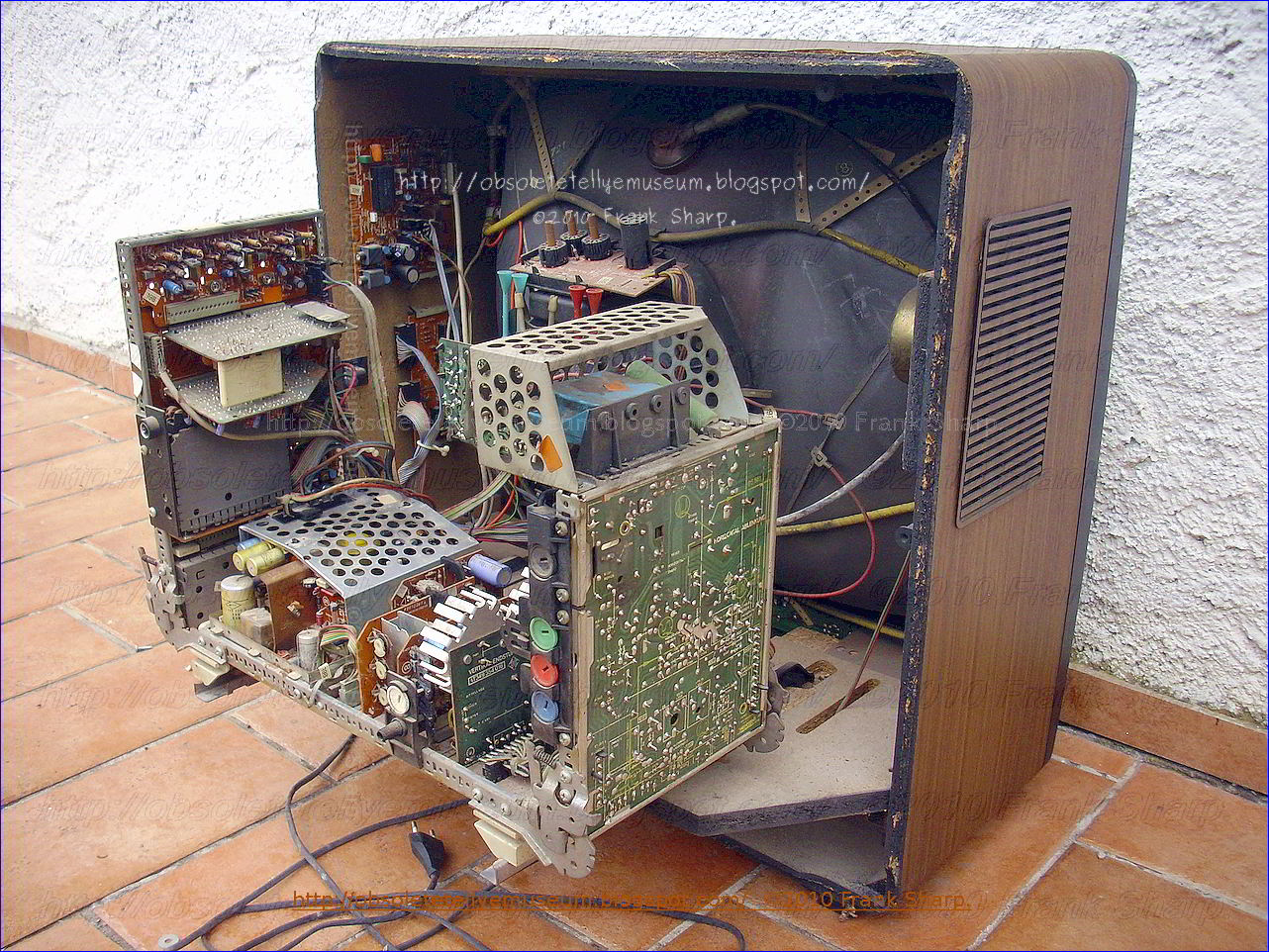


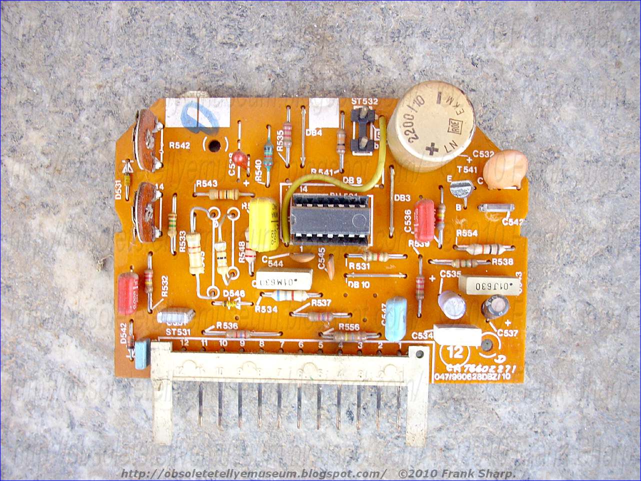


