BACKGROUND OF THE INVENTION
The present invention relates to a switching voltage regulator power supply dev

ice
combined with the horizontal deflection circuit of a television
receiver which it supplies with DC voltage. It relates, more
particularly, to DC voltage supply devices of the type which boost or
increase the voltage supplied at the output of the device in relation to
the level of a DC voltage applied to its input and which regulate this
level by recurrent switching of this input voltage, this switching being
synchronous with the (horizontal) line frequency of the television
receiver supplied by this device.
Switched step-up or boost voltage regulator devices of this type are
known, particularly from the publications U.S. Pat. Nos. 3,571,697 (or
3,736,496) and they are related to switched mode power supply devices or
DC-DC converters of the so-called unisolated flyback type, in which the
collector-emitter path of a bipolar switching transistor is connected
in series with a commutating inductance between the terminals of a DC
source supplying an input voltage and a rectifying diode is connected
between the junction of the inductance with the transistor and one of
the plates of a filtering or storage capacitor (in parallel with the
load), so that the current stored in the inductance during the
conducting period of the transistor is used for charging the capacitor
(and supplying the load) through the diode during its consecutive
cut-off period. The use of a switched-mode power supply device of this
type in television receivers for supplying, particularly, the horizontal
deflection circuit thereof has been described, for example, in two
articles by VAN SCHAIK entitled respectively "AN INTRODUCTION TO
SWITCHED-MODE POWER SUPPLIES IN TV RECEIVERS" and "CONTROL CIRCUITS FOR
SMPS IN TV RECEIVERS," appearing respectively on pages 93 to 108 of No.
3, Vol. 34, of September 1976 and on pages 162 to 180 of No. 4 of this
same volume, of December 1976, in the English language Dutch review
"ELECTRONIC APPLICATIONS BULLETIN" of PHILIPS', or on pages 181 to 195
of No. 135 of July 1977 and on pages 210 to 226 of No. 136 of October
1977 of the British review "MULLARD TECHNICAL COMMUNICATIONS." Since
none of the switched-mode power supply devices described in these
articles, isolated or not from the mains, whether they use a forward or a
flyback converter, supplies at its output a DC voltage for supplying
the horizontal deflection circuit before the switching transistor has
been turned on (saturated or conducting) one or more times, the control
circuit of this transistor must comprise an independent relaxation
oscillator and must be supplied by the same DC input voltage (rectified
and smoothed voltage of the AC mains) as the switching circuit
comprising the inductance and the transistor in series. Synchronization
of the switching with the horizontal deflection can only occur
subsequently, when the horizontal oscillator and/or the horizontal
deflection circuit as a whole have begun to operate, as soon as the
supply voltage supplied thereto by the device which operates
independently on starting up, has become sufficient. This
synchronization of the switching with the horizontal deflection,
advantageous for reducing or eliminating the interferences visible on
the screen which are caused by high-frequency energy radiation due to
abrupt transitions of power switching, particularly when the switching
transistor is being cutt off, is generally carried out by means of a
signal comprising flyback or retrace pulses, taken at the terminals of
an auxiliary secondary winding of the line tranformer whose primary
winding is generally connected between the output of the switched-mode
power supply device and one of the terminals of the trace switch which
is provided in the output stage. It is also possible to use for this
purpose the signal provided by the horizontal oscillator (see, for
example, the publication FR-A-2 040 217).
In a switched-mode supply for a television receiver described in the
publication FR-A-2 261 670, the circuit for controlling the switching
transistor of a forward-type converter, supplied with the rectified and
smoothed voltage of the mains, comprises a bistable trigger circuit of
flip-flop one of whose outputs is coupled back to one of its trigger
inputs through a regulating circuit comprising a sawtooth voltage
generator and a voltage comparator providing transitions which control
the setting of the flip-flop, when the sawtooth voltage reaches the
level of a voltage proportional to the amplitude of the flyback pulse.
The other one of the two complementary outputs of this flip-flop is
coupled back to its other trigger input through a so-called starting
loop comprising an ascending voltage wave-form which approaches
asymptotically a predetermined voltage level smaller than a
predetermined fraction of the nominal level which the amplitude of the
flyback pulse must reach in normal operation, and a voltage comparator
providing transitions which control the recurrent resetting of the
flip-flop to its initial state until the flyback pulse has reached or
exceeded a threshold amplitude slightly below its nominal amplitude.
When this threshold amplitude has been exceeded, resetting of the
flip-flop is controlled by the flyback pulses themselves, negative-going
in the present case, which supplant the starting pulses. Such an
arrangement is equivalent to an astable multivibrator during the
starting period, which later becomes a monostable one and triggered by
the flyback pulses and whose quasi-stable state has a variable duration,
depending on the amplitude of these pulses so as to obtain regulation
thereof by the duty cycle. The pulse which controls the closing of the
switch (saturation of the switching transistor) begins here with the
leading edge of the flyback pulse and its duration or length is
modulated as a function of the current drawn by the load and of the
variation of the rectified and smoothed voltage, so that its end
controlling the opening of the supply switch

(cutting off the transistor) occurs during the trace portion of the
horizontal deflection. Thus it can be seen that this switched-mode
supply, like most of the known ones, effects regulation of its output
voltage by varying the duty cycle as a reverse function of the level
thereof.
Since the high-frequency radiation is precisely at its most intense
during abrupt transitions of current in the switching inductance and of
the voltage accross its terminals, the appearance of one or more
vertical lines (light or dark according to the sense of the modulation
of the carrier wave by the video signal) may be observed, contrasting
with the normal contents of the picture, whose location on the screen
depends on the duration of the pulse controlling the switching
transistor. The effect of this radiation becomes particularly
troublesome when the input signal of the radio-frequency stages or tuner
is small, particularly when the selected channel is situated in the
lower part of the VHF band, for the automatic gain-control device of the
receiver acts on the gain of the high-frequency and/or
intermediate-frequency input stages, so that the sensitivity
(amplification) of the receiver is then maximum and this also as
concerns the spurious radiated signals.
SUMMARY OF THE INVENTION
The present invention, on the one hand, avoids or at least appreciably
reduces the interferences visible on the screen by controlling the
cutting off of the switching transistor in synchronism with the leading
edge or the flyback pulse and, on the other hand, the starting of the
horizontal deflection circuit by means of a simple circuit without any
special oscillator, and provides efficient protection of the switching
transistor which remains cut off when the horizontal deflection circuit
is not operating. This is made possible by using a step-up switching
regulator supply device of the type described in the publication U.S.
Pat. No. 3,571,697 and whose control circuit includes, in accordance
with the invention, the horizontal deflection circuit, which it
supplies.
The object of the present invention is a power supply device with
boosting and regulation of its output voltage by switching, combined
with a horizontal sweep circuit of a television receiver, which it
supplies and which comprises a horizontal oscillator, a driver stage and
an output stage including a line transformer, this device comprising an
inductance and the collector-emitter path of a switching transistor
connected in series between the poles of a DC input voltage source, a
rectifiying diode connected by its anode to the junction between the
inductance and the collector of the transistor and by its cathode to one
of the terminals of a filtering capacitor whose other terminal is
connected to the emitter of the transistor so as to supply between its
terminals an initial output voltage, slightly lower than the input
voltage, when the transistor is cut off permanently, and a regulated DC
output voltage with a level higher than the input voltage, when the
transistor is recurrently alternately turned on and off, the level of
this output voltage depending on the duty cycle of the respective states
of this transistor, and a control circuit for driving the base of the
transistor and including a regulator stage comparing an adjustable
fraction of the output voltage to a fixed reference voltage and
supplying a regulating current or voltage proportional to the difference
between these compared voltages, to a pulse-width modulator triggered
by means a recurrent signal and supplying a rectangular signal whose
duty cycle varies as a function of this regulating current or voltage,
and another driver stage receiving the rectangular signal and
controlling the switching transistor.
In accordance with the invention, the horizontal deflection forming an
integral part of the circuit controlling the switching transistor,
determines therefor, from the start, the repetition period of the
rectangular signal controlling it, and one of the supply inputs of the
other driver stage receives directly a first voltage waveform whose
positive alternations, comprise DC voltage plateaux
and
whose negative alternations comprise negative-going flyback pulses
supplied by a first secondary winding of the line transformer, so as to
control the cut-off the switching transistor substantially
simultaneously with that of the trace switch transistor.
DESCRIPTION OF THE DRAWINGS
The invention will be better understood and other of its objects,
characteristics, features and advantages will become clear from the
following description and the accompanying drawings which refer thereto,
given solely by way of example, in which:
FIG. 1 is partly a block diagram and partly a schematic diagram of a
power supply device combined with the horizontal deflection circuit in
accordance with the invention;
FIG. 2 shows waveforms of two voltages and of a current at different points of the circuit of FIG. 1;
FIG. 3 is a block diagram of the circuit for controlling the switching transistor;
FIGS. 4 and 5 are schematic diagrams of two different embodiments of the
driver circuit 20 forming the output stage of the control circuit of
FIG. 3;
FIG. 6 is the block diagram of one embodiment of the pulse-width modulator 10 of the circuit of FIG. 3;
FIG. 7 shows three voltage waveforms at different points of the circuit of FIG. 6;
FIG. 8 is a schematic diagram of one embodiment of the pulse-width
modulator 10 of the circuit of FIG. 3, using discrete components;
FIG. 9 shows a current waveform and two voltage waveforms at different points of the circuit of FIG. 8;
FIG. 10 is a schematic diagram of a conventional embodiment of a
regulator stage 30 adapted to supply the modulation input of the
modulator of FIG. 8; and
FIGS. 11 and 12 are partial respective schematic diagrams of two
embodiments of a power supply device in accordance with the invention.
DESCRIPTION OF THE PREFERRED EMBODIMENTS

FIG.
1 shows the schematic diagram of the power stages of the power supply
device and of the horizontal deflection circuit of the television
receiver, which it supplies and in block diagram form the respective
circuits which control them.
The DC input voltage VE which is not regulated is supplied by a
rectifier bridge R with four diodes, supplied at its input by the
secondary winding of an insulating step-down transformer TS, whose
primary winding is supplied by the AC mains. The output terminals of
rectifier bridge R are connected respectively to the terminals of a
first filtering capacitor C1 across which this input voltage VE is
taken.
The positive pole P of this source of the input voltage VE is connected
to one of the terminals of an energy-storage inductance L, whereas its
negative pole N is connected to ground G of the receiver, which is
isolated from the mains. The other terminal of inductance L is
connected, on the one hand, to the collector of a first NPN bipolar
switching transistor T1, whose emitter is connected to ground G and, on
the other hand, to the anode of a first diode D1 whose cathode is
connected to the positive terminal of a second filtering and storage
capacitor C2. With the negative terminal of this second capacitor C2
connected to ground G, the output voltage VS which supplies the load is
taken between its terminals.
Such a supply device BS provides both step-up or boost and regulation of
its output voltage level, because the first switching transistor T1 and
the first diode D1 thereof are connected so as to conduct respectively
currents flowing through inductance L in the same direction, it supplies
at its output formed by the terminals of the second capacitor C2, an
initial DC voltage VSI as soon as the primary winding of the insulating
transformer TS is connected to the mains. This initial voltage VSI which
is equal to the input voltage VE less the forward voltage drop VD1
across the first diode D1, is then supplied to the load until the
control circuit SC is started up, whose output 6 is connected to the
base of the first transistor T1 so as to cause it to be alternately
turned on and off.
When the first transistor T1 is turned on by positively biasing its
base-emitter junction, its collector-emitter path connects the junction
of the inductance L with the anode of the first diode D1 to ground G.
Diode D1 being then reversely biased, it ceases to conduct and the
inductance L connected by the first transistor T1 between the positive P
and negative N poles of the source supplying the unregulated DC input
voltage VE, then conducts a linearly increasing current IL so as to
store the energy which increases with the square of the conduction
duration of the first transistor T1, until this latter is cut off. At
the instant when the first transistor T1 is cut off after the control
circuit SC has brought its base-emitter voltage to zero or below, the
voltage at the terminals of inductance L is reversed so that, at its
junction with the collector of transistor T1 and the anode of diode D1,
there appears a voltage VM greater than the input voltage VE, which
results in the forward biasing of diode D1. Consequently, from the
instant when transistor T1 is cut off, diode D1 conducts a linearly
decreasing current until the energy stored in the form of a current IL
in the inductance L, which charges the second capacitor C2 to an output
voltage VS greater than the input voltage VE, disappears. The regulation
of the level of the output voltage VS is here effected in a
conventional way, by varying the duty cycle, i.e. the radio (quotient)
between the duration of the conducting period of transistor T1 and the
sum of the respective durations of two of its successive conducting and
cut off periods, as a function of the desired output voltage VS
(determined by comparison to a stable reference voltage).
According to the invention, a supply device BS of the above-described
type is combined with the horizontal deflection circuit SH of a
television receiver, which it supplies, so that this latter forms an
integral part of its control circuit SC and for determining the
repetition period of its operation and so that the above-mentioned
regulation by varying the duty cycle maintains a stable peak-to-peak
amplitude of the sawtooth scanning current and/or the very high voltage
for biasing the electrodes (anode, focusing electrode and accelerating
grid) of the cathode-ray tube, which are obtained by rectifying the
horizontal flyback pulses supplied by a step-up secondary winding (not
shown) of the line transformer TL.
The horizontal deflection circuit SH which comprises in cascade the
horizontal oscillator OH whose known phase control circuit with respect
to the horizontal sync signal separated from the composite video signal
has not been shown here, the driver stage HD controlled by the
horizontal oscillator OH and controlling the output stage OS of the
horizontal deflection, is as a whole supplied by the above-described
regulated power supply device BS. In fact, the positive supply input AL
of the horizontal deflection circuit SH is connected by means of a fuse
FS to the junction of the cathode of the first diode D1 with the
positive terminal of the second capacitor C2, which forms the positive
output terminal SP of the regulated power supply device BS. This supply
input AL is connected directly to that of the driver circuit HD and,
preferably, through a conventional Zener diode or series ballast
transistor voltage regulator VR, to that of the horizontal oscillator
OH, which are moreover connected to the isolated ground G.
The supply input AL of the horizontal deflection circuit SH is
furthermore connected to one of the primary winding terminals B1 of the
line transformer TL, whose other terminal AB is connected in parallel to
the collector of another switching transistor TH, of NPN type, called
trace switch transistor, to the cathode of a second so-called shun
t
recovery diode DR, to one of the terminals of another capacitor CR,
called line-retrace capacitor, and to one of the plates of an additional
capacitor CS, called trace capacitor, which supplies the horizontal
deflection coils LH one terminal of which is connected to its other
terminal during the trace periods of the scanning. The emitter of the
scanning transistor TH, the anode of the "shunt" recovery diode DR, the
other terminal of the retrace capacitor CR and the other terminal of the
horizontal deflection coils LH are all connected to ground G. This
assembly of components thus connected forms the output stage OS whose
operation is well-known and does not form part of the invention.
As was mentioned above, as soon as the primary winding of the step-down
isolating transformer TS is connected to the mains, rectifier R supplies
the first filtering capacitor C1 so as to provide between its terminals
P and N a unregulated low DC voltage VE. With the first transistor T1
then turned off, this input voltage is applied through the inductance L
and the first diode D1 to the second capacitor C2 so as to obtain
between the terminal SP and ground G an initial output voltage VSI
substantially equal to VE-VD1, which is approximately equal to 60
percent of the regulated output voltage VS. This initial output voltage
VSI (equal to about 0.6 VS) is sufficient to cause the generation of
autonomous oscillations by the horizontal oscillator OH. This latter
supplies at its output, connected to the input of driver circuit HD,
pulses at an independent frequency close to the line frequency. In
response to these pulses, driver circuit HD, also supplied by device BS,
provides at the base of the trace switch transistor TH pulses
controlling its periodical cut off at this independent frequency and its
consecutive turning on after a period greater than the duration of the
flyback period, so that the recovery diode DR may take the current from
the deflector LH during substantially the first half of the trace
portion of the scan. During flyback or retrace, with both transistor TH
and diode DR cut off, the energy stored in the form of currents
respectively in the inductances of deflector LH and of the primary
winding B1 of the line transformer TL which are then, from the AC
current point of view, connected in parallel, flow in an oscillating
manner through the retrace capacitor CR which forms therewith a parallel
resonant circuit whose resonance period determines the duration of the
flyback period.
There then appears periodically between point AB and ground G a voltage
pulse VTH having substantially a sinusoidal half-wave form, which is
shown in Diagram A of FIG. 2. The average value of this voltage VTH
being then equal to VSI, at start-up, and to VS, during established
operation. The line transformer TL comprises, in addition to a
very-high-voltage winding and other windings for supplying rectifying
circuits, not shown, two secondary windings B2, B3 respectively
supplying across their terminals, voltage waveforms comprising flyback
pulses with zero average values and with respectively negative and
positive polarities.
This means that the first secondary winding B2 supplies a voltage
waveform -VTL which, between two successive flyback pulses, comprises a
positive plateau whose level is equal to the average value of these
pulses and which is used, in accordance with the invention, to control
the turn off of the first transistor T1 so that the interferences which
would otherwise be visible only occur during the line-blanking periods
comprising the line-retrace periods. The second secondary winding B3
then supplies a voltage waveform +VTL which is the reverse of or
complementary to the preceding one -VTL.
O

ne
of the terminals of each of these secondary windings B2, B3 is
connected to ground G, whereas their other terminals are respectively
connected to two inputs 2 and 1 of the control circuit SC. A third input
3 of this latter is connected to the SP output of the supply device BS
and a fourth input 4 is connected to the positive pole P of the input
voltage source VE. A fifth terminal 5 of the control circuit SC is
connected to ground G (or negative pole N) and its output 6 is connected
to the base of the first transistor T1. This control circuit SC causes,
following the start up of the horizontal deflection circuit SH, a first
saturation of the first transistor T1 at a time determined by a
pulse-width modulator operating by conventional comparison of a sawtooth
voltage waveform the elaboration of which is controlled by a first
flyback pulse, with a regulating voltage, depending on the output
voltage VS. During this saturation period of transistor T1 which extends
as far as the leading edge of the next flyback pulse, energy is stored
in inductance L.
From the instant when transistor T1 is turned off, diode D1 transfers
this stored energy to the second capacitor C2, at the terminals of which
it causes an increase of the voltage VS with respect to its initial
value VSI, until the current in diode D1 is canceled out, when it
becomes reverse biased.
The collector-emitter voltage waveforms VTH of the trace switch
transistor TH and VCE of the switching transistor T1 in established
operation have been shown respectively by the diagrams A and B of FIG.
2. Diagram C of FIG. 2 shows the corresponding waveform of the current
IL flowing through the inductance L.
When the base of the first transistor T1 receives from the output 6 of
the control circuit SC a rectangular signal which turns it on at time
instant t1, its collector-emitter voltage VCE (Diagram B) becomes close
to zero (V
CEsat ) and a linearly increasing current IL
(Diagram C) flows through inductance L from time t1 until time t2 when
transistor T1 is again turned off, which is controlled by the leading
edge of the flyback pulse VTH (Diagram A). With the collector current of
transistor T1 canceled at the end of the storage time of the excess
minority carriers in the base, the voltage across the terminals of the
inductance L inverses its polarity so as to be added to the input
voltage VE, so that the collector-emitter voltage VCE (Diagram B) then
reaches a level VM greater than VS (as well as VE), so as to apply
forward bias to the first diode D1, which then conducts the current IL
through the inductance L. This current IL, from time instant t2 when it
reaches its maximum value IM, becomes linearly decreasing and it flows
through the first diode D1 in the passing direction in order to recharge
the second capacitor C2 and supply, in particular, the horizontal
deflection circuit SH.
When the current IL passing through the first diode D1 is canceled out
at time t3, the collector-emitter voltage VCE of the first transistor T1
becomes equal to the unregulated input voltage VE until the next turn
on of the transistor T1, and the first diode D1 remains reversely biased
until the time when this latter is cut off again.
From the above it can be easily seen that the principal advantage of
this combined device resides in the fact that a single oscillator OH
belonging to the horizontal deflection circuit SH is sufficient for
controlling the two power switching transistors TH and T1.
Furthermore, a possible overload in the circuitry of the television
receiver, such for example as a short-circuit of the trace switch
transistor TH, results in overloading the diode D and the inductance L.
The first transistor T1 which is consequently cut off is not subjected
to this overload and is therefore protected. In order to protect the
rest of the television receiver as well as inductance L and the first
diode D1, a fuse FS may be connected in series in the supply line from
the second capacitor C2. This fuse FS may also be inserted between pole P
and inductance L.
It is moreover known that it is difficult to construct switched supplies
for obtaining correct operation when it is not fully charged (for
supplying, for example, a ready-state remote-control receiver). In the
present case, the problem does not come up since, when the supply is in
operation, there is always a minimum load formed by the horizontal
deflection circuit. When this circuit is not operating, the supply
circuit BS does not operate either, but it supplies an output voltage
VSI of a value less than the nominal voltage VS which cannot cause
damage and which may, for example, supply a ready-state receiver for
television receivers having a remote control.
Finally, the control circuit SC allows transistor T1 to be cut off at
the beginning of each flyback period, when the blanking circuit has
extinguished the spot (s) on the cathode-ray tube. Thus, the spurious
signals radiated into the receiver input circuits will cause no visible
effect on the screen of the cathode-ray tube.
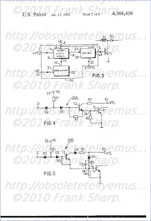
FIG. 3 shows in block diagram form the control circuit SC of FIG. 1.
This control circuit SC comprises a pulse-width modulator stage 10 a
first input 11 of which, connected to input 1, receives flyback pulses
of positive polarity +VTL from the second secondary winding B3 of the
line transformer TL (see FIG. 1 and a second input 12 of which receives a
so-called regulating voltage or current whose level is proportional to
the difference between the actual output voltage VS and a constant
reference value, delivered by the output 32 of a regulating circuit or
stage 30 whose input 31 is connected through input 3 to the positive
output pole SP of the supply device BS supplying the regulated voltage
VS. The variation of the regulating current or voltage causes the
variation of the time instant when the instantaneous amplitude of a
sawtooth voltage waveform, either with substantially constant slope and
amplitude, reaches the level of this regulating voltage, or with a slope
variable depending of the regulating current (which is added to the
current for linearly charging a capacitor), reaches the predetermined
level of a fixed reference (threshold) voltage, with respect to the
beginning or the end of the sawtooth waveform. Thus a two-level
rectangular signal with constant periodicity is generated, whose duty
cycle varies as a function of the regulating current or voltage. If it
is arranged, which is possible, for a reduction of the output voltage VS
with respect to its nominal value defined by the reference voltage, to
cause an increase in the duty cycle and for an increase in VS to have
the opposite effect, regulation of this output voltage VS is provided,
which tends to be stabilized to this nominal value.
The output 14 of modulator 10 supplies a first input 21 of the driver
stage 20 of the first switching transistor T1, a second input 22 of
which receives the flyback pulses of negative polarity -VTL, coming from
the first secondary winding B2 of the line transformer TL.
FIGS. 4 and 5 illustrate two different embodiments of the driver stage
20 of FIG. 3, providing efficient turn off of the first transistor T1.
In FIG. 4, the driver stage 20A comprises a third supply input 23 which
connected to the positive pole (P) of the source of the (unregulated)
input voltage VE and to one of the terminals of a first resistor R1 (1.8
kiloohms) whose other terminal is connected in parallel to the anodes
of two diodes D2 and D3 (of type 1N4148). The second of these diodes D3
has its cathode connected to the base of a third NPN transistor T2 and
to one of the terminals of a second resistor R2 (220 ohms). The emitter
of the third transistor T2 is connected to the other terminal of the
second resistor R2 and to the o
utput
24 of stage 20A, which is connected through the output 6 of the control
circuit SC to the base of the first transistor T1. The collector of the
second transistor T2 is connected through a third resistor R3 (10 ohms)
to the second input 22 of stage 20A receiving the signal -VTL which
comprises the negative-going flyback pulses and, between them, plateaux
of a constant positive level (zero average value). The base of the first
transistor T1 is coupled to its emitter and to ground G, through a
fourth resistor R4 (100 ohms). The third transistor T2 is thus mounted
as a common collector (emitter-follower) stage.
When the output 14 of modulator 10 (FIG. 3) which is connected to the
input 21 of stage 20A supplies a low state (level), i.e. a voltage close
to zero, the thus positively biased diode D2 becomes conducting so that
its anode will be at a voltage of a few tenths of a volt (0.7+V
CEsat )
which is less than the voltage required for making the three series PN
junctions orientated in the same direction conductive, the first of
which is formed by the third diode D3, the second is the base-emitter
junction of a third transistor T2 and the third that of the first
transistor T1, which will thus remain turned off. When, on the other
hand, output 14 supplies a high state or forms an open circuit (the
output stage of modulator 10 being formed by an open-collector
transistor), diode D2 is cut off by its reverse bias and the voltage VE
applied to the input 23 causes a current to flow through the first
resistor R1, the diode D3 and the respective base-emitter junctions of
transistors T2 and T1 connected in series. Under these circumstances and
if, at the same time, the voltage waveform -VTL applied to the
collector of transistor T3 presents its constant positive level portion,
coinciding with the trace periods of the horizontal scan, transistors
T2 and T1 become simultaneously saturated with the effect previously
described insofar as the supply device BS of FIG. 1 is concerned. On the
other hand, when the voltage waveform -VTL applied to the collector of
the third transistor T2 becomes negative, during flyback periods, the
current then flows between terminals 23 and 22 of driver stage 20 A,
through resistor R1, diode D3, the base-collector junction of the third
transistor T2 and resistor R3. The third transistor T2 then operates
along its symmetrical saturation characteristics, i.e. it is inverted so
that its collector becomes emitter and vice versa. It then conducts a
current in the reverse direction between ground and the input 22
(negative) through the resistor R4 across the terminals of which it
causes, after removal of the excess minority carriers from the base of
the first transistor T1 through the third transistor T2, a voltage drop
biasing said base negatively with respect to the emitter. This negative
voltage applied to the base of reversely saturated transistor T3 allows a
considerable reduction in the storage time and a rapid turnoff of the
first transistor T1. Since the sawtooth generator of the pulse-widt
h
modulator 10 described above is controlled by positive-going flyback
pulses, the rectangular signal applied by its output 14 (FIG. 14) to
input 21 of stage 20A undergoes, during the flyback period following the
turn off of the first transistor T1, a transition from its high state
to its low state which causes diode D2 to conduct and, consequently, the
third transistor T2 (reversed) to be cut off before the waveform -VTL
becomes positive again and rebiases this transistor T2 the right way
round.
FIG. 5 shows the schematic diagram of another embodiment of the driver
circuit 20 of FIG. 3, designated by 20B, which has only been modified
with respect to circuit 20A of FIG. 4 insofar as the collector circuit
of the third transistor T2 and the base circuit of the first transistor
T1 are concerned.
This modification is more particularly intented for the case where the
negative peak amplitude of the voltage waveform -VTL applied to the base
of the first transistor T1 through resistor R3 and the
emitter-collector path of the reversely saturated third transistor T2,
exceeds the reverse (Zener) avalanche-effect breakdown voltage of one of
the base-emitter or base-collector junctions of the first transistor
T1. This may occur when the first secondary winding B2 of the line
transformer TL is also used for other functions in the television
receiver.
To prevent the third transistor T2 from being reversely saturated
(symmetrically), the circuit 20B comprises a fourth diode D4 inserted
between the input 22 receiving the voltage waveform -VTL and the
collector thereof, in series with the resistor R3 and connected to
conduct in the same direction as its collector-emitter path. The input
22 is more over connected to the cathode of a fifth diode D5 (1N4148)
whose anode is connected through a circuit formed by a fifth resistor R5
(330 ohms) and a third capacitor C3 (1nF) connected in parallel, to the
base of the first transistor T1.
Diode D5 isolates the base of transistor T1 from the input 22, when the
waveform -VTL is positive, and connects them together through a
resistive voltage divider formed by resistors R5 and R4 in series, when
it becomes negative. Capacitor C3 accelerates the turn-off by favoring
the transmission to the base of T1 of abrupt transitions of the negative
flybacd pulses.

FIG.
6 is a diagram, partly in block form, of a possible embodiment of the
pulse-width modulator 10 of the control circuit SC of FIG. 3. Diagrams
D, E and F of FIG. 7 show the voltage waveforms applied respectively to
the input 11 (+VTL) and supplied by the output SI (VI) of the sawtooth
generator GD and by the output 14 (VP) of circuit 10A.
Modulator 10A of FIG. 5 comprises a sawtooth generator GD formed by a
conventional integrator circuit comprising a first amplifier A1
(integrated operational amplifier, for example), an integrating resistor
R1 inserted in series between the input 11 receiving the voltage
waveform +VTL illustrated by Diagram D of FIG. 7 and supplied by the
second secondary winding B3 of the line transformer TL, and the input
(inverting) of amplifier A1, as well as an interating capacitor CI
connected between this input and the output SI of amplifier A1
(capacitive feedback). In response to this waveform +VTL, the output of
amplifier A1 forming the output SI of sawtooth generator GD, supplies a
voltage waveform VI illustrated by the diagram E of FIG. 7 which
comprises, during the period between time instants t0 and t2
corresponding to the trace period TA of the scan, a voltage decreasing
linearly between a maximum value (positive) and a minimum value
(negative), and during the flyback intervals preceding time instant t0
and succeding to time instant t2, an increasing voltage of substantially
semi-cosinusoidal shape.
Voltage VI is applied to one of the inputs (-) of an analog voltage
comparator which may be formed by means of a second differential-type
amplifier A2 (integrated operational amplifier), whose other input (+)
connected to the input 12 of modulator 10A, receives the regulating
voltage VR supplied by the regulator stage (30 of FIG. 3). This
regulating voltage VR, which is obtained by com
paring
the output voltage VS of the supply device BS of the circuit of FIG. 1
with a reference voltage (VZ supplied by a Zener diode, for example), is
a DC voltage undergoing slow variations, shown in Diagram E of FIG. 7
by a dash-dot line.
When the waveform VI applied to the inverting input (-) of comparator A2
is greater than the regulating voltage VR, which is the case during the
period between time instants t0 and t1, its output connected to the
output 14 of modulator 10A provides a low state. When, on the other
hand, it (VI) reaches or becomes less than VR, which occurs from the
time instant t1, the output 14 of modulator 10A provides a high state
(which causes saturation of the first transistor T1). This high state
continues until time instant t4 subsequent to the time instant t2 of the
beginning of the following flyback pulse whose leading edge controls
the turn-off of the first transistor T1, when the waveform VI becomes
greater than the regulating voltage VR. Thus there is obtained at the
output 14 of modulator 10A a rectangular signal VP shown in Diagram F of
FIG. 7, formed successively of a low-level (zero or negative) beginning
during the first half of the flyback period TR and ending at time
instant t1, and a high level going from time instant t1 to time instant
t4. Time instant t1 of the positive transition of signal VP, which
determines the beginning of conduction of the first transistor T1 is
then situated during the trace period of the scan TA and its position
with respect to the beginning t0 or to the end t2 thereof varies as a
function of the regulating voltage VR. When the regulating voltage VR is
negative (as on the Diagram E of FIG. 7), a predetermined fraction of
the output voltage VS is greater than the reference voltage, the
duration of the high level state (t2-t1) is less than half of the trace
period of the scan T1. In the opposite case, this duration (t2-t1) is
greater than TA/2. The modification of this duration (t2-t1) and thus of
the duty cycle is carried out in the reverse direction of the variation
of the output voltage VS so as to stabilize it at a previously adjusted
level, with respect to this reference voltage. The waveform -VTL may
also be applied to the input 11 of modulator 10A. In this case, the
input of comparator A2 must also be inverted.
To obtain suitable operating limits, while taking into consideration
particularly the value of inductance L, the duty cycle or the durations
(t2-t1) must vary between 0, the case where the input voltage VE is
equal to the nominal output voltage VS, and about two-thirds, the case
where the maximum power is supplied for a minimum voltage at the input.
The ratio between the residual alternating voltage (hum) at the output
and the alternating voltage at the input must also allow an image to be
obtained which is not perturbed for the eye. A value less than or equal
to a hundredth for this ratio gives satisfactory results.

FIG.
8 shows the simplified diagram of a practical embodiment (by means of
discrete components) of the pulse-width modulator 10 of FIG. 3.
Different waveforms of a current I1 and input +VTL and output VP
voltages are respectively illustrated by the Diagrams H, J and K of FIG.
9.
The input 11 of modulator 10B of FIG. 3 receives the voltage waveform
+VTL which may be suppled either directly by the second secondary
winding B3 of line transformer TL, or through a coupling capacitor whose
one terminal is connected to the collector of the trace switch
transistor TH (see FIG. 1). This input 11 supplies a passive shaping
circuit, supplying negative-going (decreasing) sawtooth waveforms during
the trace periods of scan T1. This passive circuit comprises a fourth
coupling capacitor C4 (0.1μ) one terminal of which is connected to the
input 11 and the other of which is connected to one of the terminals of a
sixth resistor R6 (10 Kohms). The other terminal of this resistor R6 is
connected to one of the terminals of a seventh resistor R7 (5.6 Kohms),
to one of the terminals of a fifth capacitor C5 (5.6 nF) and to the
anode of a sixth diode D6. The other terminal of capacitor C5 is
connected to ground G. The cathode of the sixth diode D6 and the other
terminal of resistor R7 are both connected to one of the terminals of an
eighth resistor R8 (33 kohms), to that of a ninth resistor R9 (470
ohms), to that of a sixth capacitor C6 (4.7 nF) and to the regulation
input 12 of modulator 10B, which is connected to the output 32 of the
regulator stage 30 (see FIG. 3). The other terminal of capacitor C6 is
connected to ground. The other terminal of resistor R8 is connected to
the supply input 13 of modulator 10B receiving the input voltage VE. The
other terminal of the ninth resistor R9 is connected to the base of a
fourth NPN transistor T3, which forms the voltage comparator stage,
whose emitter is connected to ground and whose collector (open), which
forms the output 14 of modulator 10 B, is connected to the input 21 of
the driver stage 20A (of FIG. 4) or 20B (of FIG. 5), formed by the
cathode of the second diode D2. The value of capacitor C6 has been
chosen so as to limit the maximum negative voltage applied to the
base-emitter junction of transistor T3 to a value less than its reverse
avalanche breakdown voltage. When the input voltage waveform
+VTL
is positive, as during the major portion of the flyback periods TR,
diode D6 short-circuits resistor R7 and we have then a simple passive RC
integrator formed by resistor R6 in series and two capacitors C5 and C6
in parallel, whose output is connected to the base of transistor T3
through resistor R9. Transistor T3 becomes conducting when its base
current IB formed by the sum of currents I1 and I2 becomes positive. The
current I1 shown by an arrow in FIG. 8 and on the Diagram H of FIG. 9,
results from the application of the +VTL waveform of Diagram J to the
above-mentionned simple integrator, during its positive alternation, and
to the cascaded double integrator R6, C5, R7, C6 during its negative
plateau going from t0 to t2. During this negative voltage plateau of the
+VTL signal, the current I1 becomes negative and linearly decreasing.
When the instantaneous negative amplitude of current I1 becomes equal to
the positive current I2 shown by another arrow in FIG. 8 and by means
of a reversed constant level (-I2) shown by a broken line in diagram H
of FIG. 7, which occurs at time t1, the base current of transistor T3 is
cancelled out and this latter is cut off. Since the current I2 is due
for a large part to the regulating current IR supplied by the output of
the regulator stage (30 in FIG. 3) and proportional to the error
voltage, the duration of the cut-off state (t4-t1) of transistor T3 and,
consequently, that (t2-t1) of the saturated state of the first
transistor T1 (as well as the duty cycle) will vary reversely to the
variation of this current IR. The current IE shown by an arrow in FIG.
8, which flows through the high-value resistor R8 from the input voltage
source VE and which is one of the components with IR of current I2,
forms a small current for maintaining transistor T3 saturated in the
absence of flyback pulses and thus of horizontal deflection. The fact
that resistor R8 is supplied by the unregulated input voltage VE allows
another parameter to be added for acting on the duty cycle of transistor
T3 as a function thereof. Diagram K of FIG. 9 illustrates the
rectangular signal VP obtained at the output 14 of the modulator 10B of
FIG. 8.

FIG.
10 is a schematic diagram of a conventional regulator stage 30 of the
control circuit of FIG. 3. It is formed essentially by a well-known
circuit called differential amplifier having two inputs, the first of
which receives an adjustable fraction of the voltage to be stabilized,
formed, in the present case, by the output voltage VS of the power
supply device (BS, FIG. 1) and the second input of which receives a
stable reference voltage which is generally generated within this stage
(as in most known ballast or switched-mode voltage regulator).
The reference voltage VZ is here produced by means of a Zener diode D7
(of the BZX83C type having a stabilized Zener voltage of 7.5 V) whose
cathode is connected to the input 31 receiving the output voltage VS of
the device BS (FIG. 1) and whose anode is connected through an eleventh
resistor R11 (10 Kohms) to ground G. The second input of the
differential amplifier used here is formed by the emitter of a fifth PNP
transistor T4 which is connected to the anode of the Zener diode D7.
The voltage (VS-VZ) biasing this emitter is then fixed with respect to
the output voltage VS. The first input of the differential amplifier is
here formed by the base of transistor T4 which is biased by a
voltage-divider circuit, formed from a fifteenth resistor R15 (4.7
Kohms), a potentiometer R16 (5 Kohms) and a fourteenth resistor R14 (22
Kohms) connected in series between the input terminal 31 and ground G.
The base of transistor T4, connected to the slider of potentiometer R16
receives then a previously adjusted fraction of the output voltage VS
supplying the horizontal deflection circuit (SH), so that it forms a
constant current generator supplying a current proportional to its
emitter-base voltage which is equal to the difference (error voltage)
between the reference voltage VZ and the selected fraction of the output
voltage VS supplied by potentiometer R16. The collector of the fourth
transistor T4, connected by a tenth resistor R10 (2.2 Kohms) to the
output 32, supplies then the regulating current IR to the regulating
input (12, FIGS. 3 and 8) of the pulse-width modulator (10 or 10B, FIGS.
3 and 8).
It will be noted here that a feedback circuit comprising a twelfth
resistor R12 (5.6 Kohms) and a seventh capacitor C7 (4.7 nF) in series
connects the collector of transistor 14 to its base.
The difference between the voltage respectively provided by the
potentiometer R16 and the Zener diode D7 causes more or less heavy
conduction of transistor T4 which delivers the current IR.
In short, when the output voltage VS increases, the voltage (VS-VZ) at
the emitter of transistor T4 increases more than that applied to its
base and current IR increases. The value of I1 at which transistor T3 is
cut off increases then in absolute value and this transistor T3 is
turned off later, which reduces the conducting period of transistor T1.
The peak current in inductance L then diminishes, which causes a
reduction of the output voltage VS which comes back to its nominal
value, taking into account the residual error required for controlled
operation.
FIG. 11 shows the complete simplified diagram of a power supply device
BS of FIG. 1 whose control circuit SCA is respectively formed by the
driver circuit 20A of FIG. 4, by the modulator 10B of FIG. 8 and the
regulator stage 30 of FIG. 10, except for a few variations.
The variations concern a damping resistor R17 of 1 kiloohm shunting the
inductance L, resistor R8 and resistor R10 which are both connected
directly to the base of transistor T3 instead of being connected to the
cathode of diode D6, resistor R11 which has been omitted and a resistor
R13 which shunts the slider of potentiometer R16 to ground. These
details of construction have no influence at all on the operation of the
circuit such as it has been described above, but simply allow easier
adjustment.

Another
embodiment is shown in FIG. 12. It allows more especially a television
set to be supplied with power in which the horizontal deflection circuit
operates from a higher DC voltage VS, of about 100 volts for example,
itself obtained from an initial output voltage VSI of about 60 volts.
The operation of the circuit is fundamentally the same as that of FIG.
11 and only the differences will be described below. The components
playing the same role in both diagrams bear the same references. The
values may however be different but their dimensioning is within the
scope of a man skilled in the art. The voltage VS delivered by the power
supply is used principally in the horizontal deflection circuit which
is the component consuming most power in the television set. The power
supply circuit components receiving permanently a voltage when the
horizontal deflection circuit is not operating, but when the mains is
connected, are solely those indispensable for activating the power
supply, i.e. the first switching transistor T1 and the circuit for
measuring the output voltage in the regulator stage 300.
To simplify the driver stage 100, instead of the single switching
transistor T1, an integrated Darlington circuit T10 is used of the BU
807 type, for example. Therefore, the gain is sufficient to omit a
discrete driver transistor T2 and to connect the cathode of diode D3
directly to the base input of T10. The negative -VTH pulses, coming from
an intermediate tapping on coil B2 of the line output transformer, are
applied directly to the base of T10 through resistor R3 which is
connected in series with a diode D9 whose cathode is connected to this
intermediate tapping.
Instead of the input voltage VE, the power supply input 4 of the control
circuit SCB is fed by a voltage obtained by rectifying the positive
half-waves (plateaux) of the -VTL voltage supplied by the first
secondary winding B2, by means of a diode D8 and a capacitor C8. Thus
considerably lower voltage may be obtained than that supplying the
horizontal deflection circuit, of the order of 13 volts, for example. A
voltage of this value allows video amplification circuits as well as
other circuit
s
of the television set to be supplied while providing for these latter a
very great reliability. This voltage is applied through resistor R1 to
the anodes of diodes D2 and D3 and through resistor R8 to the base of
the transistor T3 of modulator 10B.
The regulator stage 300 here comprises two PNP transistors T4 and T5
connected differentially. For that, their emitters receive the voltage
rectified by D8 through a resistor R18 of 1.5 kiloohms. The collector of
transistor T5 is connected to ground through a resistor R20 of 3.9
kiloohms and the collector of transistor T4, which supplies the
regulating current IR, is connected to the cathode of diode D6 through a
resistor R10 of 4.7 kiloohms.
The reference voltage (6.2 volts) is supplied by a Zener diode D7 whose
anode is connected to ground, and cathode to a resistor R19 (6.8
kiloohms) which receives the voltage rectified by D8. This reference
voltage is applied to the base of transistor 14. A capacitor C9 (49
microfarads) shunts diode D7 so as to cause the reference voltage to
rise gradually when the apparatus is switched on, which allows a gradual
rise of the output voltage VS to be obtained.
A potentiometer R16 of 10 kiloohms connected between two stopper
resistors R15 (68 kiloohms) and R14 (5.6 kiloohms) receives the voltage
VS through the resistor R15 and is connected to ground through resistor
R14. The sliding contact of potentiometer R16 allows a fraction of the
voltage VS to be applied to the base T5. A resistor R13 (47 kiloohms)
also connects this base to the common point between R15 and R16.
An anti-oscillation capacitor C10 (15 nanofarads) connects the base of the collector of transistor T5.
Thus the regulating current IR supplied by resistor R10 is directly
dependent on the difference between the output voltage VS, applied to
the horizontal deflection circuit, and the reference voltage determined
by the Zener diode D7. The power supply BS thus stabilizes this voltage
VS and at the same time the rectified voltage supplied by diode D8.
To stop this power supply, as well as that of FIG. 11 moreover, it is
sufficient to stop by means of a remote control receiver, for example,
the operation of the horizontal oscillator.
In this case, the input voltage VE is still present, but is considerably
smaller than voltage VS. For the power supply of FIG. 12, this reduced
voltage is only applied to the Darlington transistor T10 and a fraction
thereof to the base of transistor T5 of the regulator stage 300. Thus
the life expectation of the other components of the device BS is
increased. Since the voltage supplied by diode D8 is itself regulated,
it may be used for supplying a major portion of the television set,
except for the horizontal deflection circuit supplied by voltage VS and
the remote control receiver which must be capable of operating
permanently (also in the ready state) so as to detect the turn-on
control signal. The protection which was mentioned earlier on is then
extended to the greatest part of the components of the television set.
It will be noted here that the three stages 10, 20 and 30 of control
circuit SC (see FIGS. 1 and 3) may be formed by means of circuits
different from those described and shown and which are known per se, and
that it is sufficient to have a secondary winding B2 (in addition to
the very-high-voltage winding) of the line transformer TL, supplying
negative line-flyback pulses which may be used for generating a
decreasing or increasing sawtooth voltage waveform as well as for
controlling the cutting off of the first switching transistor T1.
TDA1950, Line Circuits for TV Receivers (18-Pin Plastic Package)

These integrated circuits are advanced versions of the well-known types TDA1940, TDA1940F, TDA1950 and TDA1950F are identical
TBA940/950, TDA9400/9500 etc. integrated line oscillator circuits.
except the following: at pin 2 the types having the suffix "F" supply ,
They comprise all stages for sync separation and line synchronisation
horizontal output pulses of longer duration compared with the basic I
in TV receivers in one single silicon chip. Due to their high degree of
types Integration, the number of external components is very small.
This integrated circuit contains the horizontal sweep generator (HO),
the amplitude filter (AS), the sync-signal separating circuit (SA) and
the frequency/phase comparator (FP). For the purpose of suppressing
noise pulses which are caused via the operating voltage during the upper
and the lower inversion point of the horizontal sweep generator (HO)
which contains a single capacitor (C) and a first threshold stage
circuit (SS1) with two fixed thresholds, there are provided a second and
a third threshold stage circuit (SS2, SS3), to the inputs of which the
sawtooth signal is applied, and with the thresholds thereof,
approximately 2 μs prior to reaching the upper or the lower peak value
of the sawtooth signal, are being passed through thereby. The output
signal of the second threshold circuit (SS2) and the output signal of
the third thresh
old
stage circuit (SS3) which is applied via the pulse shaper circuit
(IF), are superimposed linearly and, via the stopper circuit (blocking
stage) (SP) serve to control the application of the composite video
signal (BAS) to the amplitude filter (AS), or else they are applied to a
clamping circuit which serves to apply the operating points of the
amplitude filter (AS) and/or of the sync-signal separating circuit (SA)
to such a potential that these two stages, for the time duration of
these output pulses, are prevented from operating.
1. An integrated circuit for color television receivers, comprising a
voltage- or current-controlled horizontal sweep generator (HO), an
amplitude filter (AS), a synchronizing-signal separating circuit (SA)
and a frequency/phase comparator (FP) which serves to synchronize the
horizontal sweep generator (HO), with said generator being a sawtooth
generator containing a single capacitor (C) and a first threshold stage
circuit (SS1) having two fixed thresholds, said integrated circuit
further comprising:
a second and a third threshold stage circuit (SS2, SS3) each being
supplied with the sawtooth signal on the input side, comprising each
time one threshold which, approximately 2μs prior to the reaching of
the upper or the lower peak value of the sawtooth signal, is being
passed thereby;
a pulse shaper circuit (IF) coupled to the output of said third
threshold stage circuit (SS3) which pulse shaper circuit reduces the
duration of the output pulse thereof to about the duration of the
output pulse of said second threshold stage circuit (SS2), and
a stopper circuit (blocking stage) (SP) coupled to the outputs of both
said pulse shaper circuit (IF) and said second threshold stage circuit
(SS2), said stopper circuit having a signal input to which there is
applied a composite video signal (BAS) and a signal output which is
coupled to the input of said amplitude filter (AS).
2. The invention of claim 1 wherein the outputs of both said pulse
shaper circuit (IF) and said second threshold stage circuit (SS2) are
coupled to a clamping circuit which applies the operating points of said
amplitude filter (AS) and said sync-separating signal (SA) to such a
potential that they are prevented from operating.
3. An integrated horizontal sweep circuit comprising:
a generator for generating a sawtooth signal;
an amplitude filter having an input for receiving a composite video signal and having an output;
a sync-signal separating circuit having an input coupled to said amplitude filter output and having an output;
a frequency/phase comparator having a first input coupled to said separating circuit output,
a second input receiving said sawtooth signal and an output for controlling said generator; and
a control circuit responsive to said sawtooth signal for inhibiting
said composite video signal when said sawtooth signal is within
predetermined signal level ranges about the upper and lower inversion
points of said sawtooth signal.
4. An integrated circuit in accordance with claim 3 wherein:
said generator comprises a capacitor, circuit means for charging and
discharging said capacitor, and a first threshold circuit controlling
said circuit means in response to said sawtooth signal reaching a first
level corresponding to said first inversion point and a second level
corresponding to said second inversion point.
5. An integrated horizontal sweep circuit comprising:
a sawtooth signal generator;
an amplitude filter having an input receiving a composite video signal and having an output;
a sync-signal separating circuit having an input coupled to said amplitude filter output and having an output;
a frequency/phase comparator having a first input coupled to said
separating circuit output, a second input receiving said sawtooth signal
and an output for controlling said generator; and
a control circuit responsive to said sawtooth signal for inhibiting
operation of said amplitude filter and/or said sync-signal separating
circuit when said sawtooth signal is within predetermined signal level
ranges about the upper and lower inversion point of said sawtooth
signal.
6. An integrated circuit in accordance with claim 5 wherein:
said generator comprises a capacitor, circuit means for charging and
discharging said capacitor and a first threshold circuit controlling
said circuit means in response to said sawtooth signal reaching a first
level corresponding to said first inversion point and a second level
corresponding to said second inversion point.
Description:
BACKGROUND OF THE INVENTION
The invention relates to an integrated circuit for (color) television
receivers, comprising a voltage- or current-controlled horizontal-sweep
generator,
an amplitude filter, a synchronizing signal separating circuit
(sync-separator) and a frequency/phase comparator which serves to
synchronize the horizontal sweep generator which is a sawtooth generator
consisting of a single capacitor and of a first threshold stage having
two fixed switching thresholds, cf. preamble of the patent claim. Such
types of integrated circuits, for example, are known from the
technical journal "Elektronik aktuell", 1976, No. 2, pp. 7 to 14 where
they are referred to as TDA 9400 and TDA 9500.
Especially on account of the fact that the amplitude filter as well as
the horizontal sweep generator in the form of the aforementioned
sawtooth generator, are integrated on a single semiconductor body, it
is likely that noise interference pulses coming from the individual
stages, and via the supply voltage line, may have a disturbing
influence upon the horizontal sweep generator, i.e. upon the threshold
stage thereof, in such a way that either the lower or the upper or
successively both switching thresholds are exceeded before the time by
the voltage at the capacitor, owing to the noise superposition, so that
the generator will show to have a "wrong" frequency or phase position.
This frequency/phase variation, of course, is compensated for by the
circuit, with the aid of the synchronzing pulses, but only in such a
way that the noise effect remains visible in the television picture.
SUMMARY OF THE INVENTION
The invention is characterized in the claim is aimed at overcoming this
drawback by solving the problem of designing an integrated circuit of
the type described in greater detail hereinbefore, in such a way that
noise pulses acting upon the capacitor voltage or the internal reference
voltages for the switching thresholds (see below) in the proximity of
the two switching thresholds, are prevented from having the described
disadvantageous effect. Accordingly, an advantage of the invention
results directly from solving the given problem.
Other objects, features and advantages of the present invention will
become more fully apparent from the following detailed description of
the preferred embodiment, the appended claims and the accompanying
drawing in which:
BRIEF DESCRIPTION OF THE INVENTION
The invention will now be described in greater detail with reference to
the accompanying drawing. This drawing, in the form of a schematical
circuit diagram, shows the construction of an integrated circuit
according to the invention.
DETAILED DESCRIPTION OF THE INVENTION
The horizontal sweep generator HO comprises the capacitor C as connected to the zero point of the circuit, and which is char
ged
and discharged via the two shown constant current sources CS1 and CS2,
thus causing the intended sawtooth voltage to appear thereat.
Moreover, the horizontal sweep generator HO comprises the first
threshold stage circuit SS1, having an upper and a lower threshold. As
soon as the capacitor voltage exceeds one of the thresholds, the first
threshold stage circuit SS1 switches over to the other threshold. The
two thresholds are defined by the voltage divider P as connected to the
operating voltage U, and in which the corresponding threshold inputs
are connected to corresponding tapping points. The output of the
threshold stage circuit SS1 controls the electronic switch S, so that
the constant current source CS2 as connected thereto, is either
disconnected from or connected to the zero point of the circuit.
Accordingly, in the disconnected state, the capacitor C is charged via
the constant current source CS1 arranged in series therewith while in
the connected state the capacitor C is discharged across the
aforementioned constant current source CS2 arranged in parallel
therewith, if, as a matter of fact, the current of the constant current
source CS1 arranged in series with the capacitor C, is smaller than
that of the parallel-arranged constant current source CS2.
Now, for the purpose of avoiding the aforementioned drawbacks, there is
provided a second and a third threshold stage circuit SS2 and SS3,
respectively, as well as the pulse shaper circuit IF. To the respective
input of the two threshold stage circuits SS2, SS3, there is applied
the capacitor voltage, in the form of the sawtooth signal, and these
stages have a threshold voltage which, approximately 2 μs prior to the
reaching of the upper or the lower peak value of the sawtooth voltage,
is being passed thereby. This means to imply that the threshold voltage
of the second threshold stage circuit SS2 is somewhat lower than the
voltage of the upper threshold of the first threshold stage circuit
SS1, and that the threshold voltage of the third threshold stage
circuit SS3 is somewhat higher than the voltage of the lower threshold
of the first threshold stage circuit SS1. The two thresholds of the
threshold stage circuits SS2, SS3 can thus be realized in a simple way
by providing further tapping points at the voltage divider P, as is
shown in the accompanying drawing. Thus, the second threshold stage
circuit SS2 is provided for at a voltage divider tapping point below
the tapping point chosen for the upper threshold, and the tapping point
for the third threshold stage circuit SS3 is provided for above the
tapping point which has been chosen for the lower threshold of the
first threshold stage circuit SS1.
Since, within the area of the lower inversion point of the sawtooth
signal there results an excessively wide output pulse of the third
threshold stage circuit SS3, the pulse shaper circuit IF is arranged
subsequently thereto, for reducing the duration of the output pulse as
applied to its input, to about the duration of the output pulse of the
second threshold stage circuit SS2. This pulse shaper circuit IF, for
example, may be realized by a monoflop, in particular by a digital
monoflop (=monostable circuit).
The output pulses of the second threshold stage circuit SS2 and of the
pulse shaper circuit IF are then super-positioned linearly, with this
being denoted in the drawing by a simple interconnection of the two
respective lines. The combined signal is applied to the input of the
stopper circuit (blocking stage) SP, to the signal input of which there
is fed the composite video signal BAS, and the output thereof controls
both the amplitude filter AS and the
synchronizing signal separating circuit SA.
The combined signal may also be used to control a clamping circuit
applying the operating points of the amplitude filter AS and/or of the
sync-signal-separating circuit SA to such a potential which prevents it
from operating.
If now the sawtooth signal reaches the range of its upper or its lower
inversion point, the composite video signal BAS is not applied to
either the amplitude filter AS or the sync-signal separating circuit
SA, so that shortly before and shortly after the inversion points,
signals are prevented from being processed in the two stages AS, SA.
This, in turn, has the consequence that during these times noise pulses
are prevented from superimposing upon the operating voltage U, so that
there is also prevented an unintended triggering of the first
threshold stage circuit SS1.
Moreover, it is still shown in the drawing that the amplitude filter
AS, the sync-signal separating circuit SA and the frequency/phase
comparator FP are arranged in series in terms of signal flow, with the
latter, in addition, receiving the sawtooth signal, and with the output
signal thereof acting upon the two current sources in a regulating
sense. In the drawing, this is indicated by the setting arrows at the
two current sources.
While the present invention has been disclosed in connection with the
preferred embodiment thereof, it should be understood that there may be
other embodiments which fall within the spirit and scope of the
invention as defined by the following claims.
PHILIPS TDA3505 Video control combination circuit with automatic cut-off control
GENERAL DESCRIPTION
The TDA3505 and TDA3506 are monolithic integrated circuits which perform video control functions in a PAL/SECAM

decoder. The TDA3505 is for negative colour difference signals -(R-Y), -(B-Y) and the TDA3506 is for positive colour
difference signals +(R-Y), +(B-Y).
The required input signals are: luminance and colour difference (negative or positive) and a 3-level sandcastle pulse for
control purposes. Linear RGB signals can be inserted from an external source. RGB output signals are available for
driving the video output stages. The circuits provide automatic cut-off control of the picture tube.
Features
· Capacitive coupling of the colour difference and
luminance input signals with black level clamping in the
input stages
· Linear saturation control acting on the colour difference
signals
· (G-Y) and RGB matrix
· Linear transmission of inserted signals
· Equal black levels for inserted and matrixed signals
· 3 identical channels for the RGB signals
· Linear contrast and brightness controls, operating on
both the inserted and matrixed RGB signals
· Peak beam current limiting input
· Clamping, horizontal and vertical blanking of the three
input signals controlled by a 3-level sandcastle pulse
· 3 DC gain controls for the RGB output signals (white
point adjustment)
· Emitter-follower outputs for driving the RGB output
stages
· Input for automatic cut-off control with compensation for
leakage current of the picture tube
Notes
1. < 110 mA after warm-up.
2. Values are proportional to the supply voltage.
3. When V11-24 < 0,4 V during clamping time - the black levels of the inserted RGB signals are clamped on the black
levels of the internal RGB signals.
When V11-24 > 0,9 V during clamping time - the black levels of the inserted RGB signals are clamped on an internal
DC voltage (correct clamping of the external RGB signals is possible only when they are synchronous with the
sandcastle pulse).
4. When pins 21, 22 and 23 are not connected, an internal bias voltage of 5,5 V is supplied.
5. Automatic cut-off control measurement occurs in the following lines after start of the vertical blanking pulse:
line 20: measurement of leakage current (R + G + B)
line 21: measurement of red cut-off current
line 22: measurement of green cut-off current
line 23: measurement of blue cut-off current
6. Black level of the measured channel is nominal; the other two channels are blanked to ultra-black.
7. All three channels blanked to ultra-black.
The cut-off control cycle occurs when the vertical blanking part of the sandcastle pulse contains more than 3 line
pulses.
The internal blanking continues until the end of the last measured line.
The vertical blanking pulse is not allowed to contain more than 34 line pulses, otherwise another control cycle begins.
8. The sandcastle pulse is compared with three internal thresholds (proportional to VP) and the given levels separate
the various pulses.
9. Blanked to ultra-black (-25%).
10. Pulse duration ³ 3,5 ms.


A SCART Connector (which stands for Syndicat des Constructeurs d'Appareils Radiorécepteurs et Téléviseurs) is a standard for connecting audio-visual equipment together. The official standard for SCART is CENELEC document number EN 50049-1. SCART is also known as Péritel (especially in France) and Euroconnector but the name SCART will be used exclusively herein. The standard defines a 21-pin connector (herein after a SCART connector) for carrying analog television signals. Various pieces of equipment may be connected by cables having a plug fitting the SCART connectors. Television apparatuses commonly include one or more SCART connectors.
Although a SCART connector is bidirectional, the present invention is concerned with the use of a SCART connector as an input connector for receiving signals into a television apparatus. A SCART connector can receive input television signals either in an RGB format in which the red, green and blue signals are received on Pins 15, 11 and 7, respectively, or alternatively in an S-Video format in which the luminance (Y) and chroma (C) signals are received on Pins 20 and 15. As a result of the common usage of Pin 15 in accordance with the SCART standard, a SCART connector cannot receive input television signals in an RGB format and in an S-Video format at the same time.This kind of connector is todays obsoleted !Consequently many commercially available television apparatuses include a separate SCART connectors each dedicated to receive input television signals in one of an RGB format and an S-Video format. This limits the functionality of the SCART connectors. In practical terms, the number of SCART connectors which can be provided on a television apparatus is limited by cost and space considerations. However, different users wish the input a wide range of different combinations of formats of television signals, depending on the equipment they personally own and use. However, the provision of SCART connectors dedicated to input television signals in one of an RGB format and an S-Video format limits the overall connectivity of the television apparatus. Furthermore, for many users the different RGB format and S-Video format are confusing. Some users may not understand or may mistake the format of a television signal being supplied on a given cable from a given piece of equipment. This can result in the supply of input television signals of an inappropriate format for the SCART connector concerned.