NORDMENDE SPECTRA COLOR SC1032 CHASSIS F6TT Controlled power supply for a television receiver equipped with remote control:BLAUPUNKT SWITCH MODE POWER SUPPLY.Blaupunkt-Werke GmbH (Hildesheim, DT)
NORDMENDE SPECTRA COLOR Chassis F6TT Power Supply view.
SMPS supply with S2530A (TOSHIBA) Chassis F6TT Power Supply view.
A
single isolation transformer supplies both the remote control
receiver and the television receiver. A pulse generator such as a
blocking oscillator which energizes the primary winding of the
isolation transformer has its pulse width controlled in response
to the loading of the circuit of the secondary winding of the
isolation transformer, as measured by the voltage across a resistor
in the circuit of a primary winding. This measuring resistor is
interposed between the emitter of the switching transistor of
the blocking oscillator and the receiver chassis. A transistor
switching circuit for cutting off the low voltage supply to the
scanning circuit oscillators of the television receiver is
responsive to the output of the remote control receiver, to a
signal from an operating control of the television receiver, and
to an indication of overcurrent in the picture tube,
independently.
1. A power supply circuit for a television receiver equipped for remote control comprising, in combination:
an
on-off switch for connecting and disconnecting the television
receiver and its power supply circuit respectively to and from the
electricity supply mains;
pulse generating means arranged for energization through said on-off switch;
an isolation transformer having its primary winding supplied with the output of said pulse generating means;
a
power conversion circuit connected to the secondary winding of
said isolation transformer for energization thereby, for supplying
an operating voltage for the scanning circuits of the television
receiver and for supplying a plurality of other voltages to
said receiver, at least one of which other voltages is also
supplied to said scanning circuits;

a
remote control signal receiver for remote control of said
television receiver and controlled switching means responsive to said
remote control receiver for switching said television receiver
between a stand-by condition and an operating condition, both
said remote control receiver and said controlled switching means
being connected to a secondary winding of said isolation
transformer for energization thereby, said controlled switching
means having a switching path for connecting and disconnecting
said scanning circuits of said television receiver respectively
to and from a source of said operating voltage in said power
conversion circuit and
means for reducing energy transfer
through said pulse generating means to said isolation
transformer when said television receiver is in the stand-by
condition.
2. A power supply circuit as defined in claim 1,
in which said pulse generating means includes rectifying means
energized through said on-off switch for supplying direct
current for energization of said pulse generating means.
3. A power supply circuit as
defined in claim 2, in which said energy transfer reducing means
includes means for varying the width (duration) of pulses
generated by said pulse generating means in response to the
extent of loading of the secondary circuit of said isolating
transformer as measured in the primary circuit of said transformer.
4. A power supply circuit
as defined in claim 2, in which said pulse generating means
includes a blocking oscillator and said energy transfer reducing
means includes means for reducing the width (duration) of the
pulses generated by said blocking oscillator.
5. A power supply circuit as defined in claim
4, in which said blocking oscillator includes a switching
transistor (5) and a load measuring resistor (7) interposed in a
connection between the emitter of said switching transistor and
the receiver chassis, and in which said pulse width reducing
means is responsive to the voltage drop across said load
measuring resistor. 6. A
power supply circuit as defined in claim 5, in which said pulse
width reducing means includes a controllable resistance (10) in
the circuit of said blocking oscillator controlled in response to
the voltage drop across said load measuring resistor.
7. A power supply circuit as defined
in claim 1, in which said operating voltage connected and
disconnected to said scanning circuits by said controlled
switching means is the low voltage supply voltage (U 3') of the
line scan and picture scan oscillators of the television receiver
and in which said controlled switching means is controlled so as
to switch off said low voltage supply voltage to put the
television receiver in the stand-by condition.
8. A power supply circuit as defined in claim
7, in which said controlled switching means includes a first
switching transistor (15) at the collector of which there is
applied a direct current supply voltage (U 3) energized through
said isolating transformer and a second switching transistor
(24) for controllably short-circuiting the base bias of said
first switching transistor, whereby a stabilized low voltage (U
3') exists at the emitter of said first switching transistor
(15) when a positive signal is supplied from an operating control
of the television receiver or from said remote control receiver
to the base of said second switching transistor (24).
9. A power supply circuit as defined
in claim 7, in which said controlled switching means is
responsive independently to an overcurrent condition in the
picture tube for switching off said low voltage supply voltage
(U 3') in response to said overcurrent condition.
Description:
The
present invention relates to a power supply unit including a
blocking oscillator for utilization with a television receiver
provided with ultrasonic remote control, and more particularly to a
television receiver the operating conditions of which are normal
operation, a stand-by operation, and the turned-off condition,
and a power supply unit therefor that includes an isolating
transformer.
In recent times television receivers have
frequently been provided with ultrasonic remote control devices
for the purpose of offering easier control. As more and more
television receivers are utilized in combination with additional
equipment, it becomes increasingly necessary to connect the
receivers only indirectly to the electric power mains (house
wiring). In a known advantageous solution of this problem, a
power supply unit includes an isolating transformer which is wired up
with a blocking oscillator in the primary circuit. The blocking
oscillator is supplied with a d-c voltage which is obtained by
rectification of the supply voltage. Compared to the isolating
transformers which are directly mains-operated, these so-called
switch-mode power supply units have the advantage that they can
be made in considerably smaller size, as they are operated at a
significantly higher frequency, and the further advantage that
they require less expensive means for rectification.
It is
necessary to supply television receivers equipped with ultrasonic
remote control with the possibility for a stand-by operation in
which only the ultransonic receiver is supplied with power and,
in some cases, also the heating current for the picture tube.
Usually a separate power supply unit is provided for the
ultrasonic receiver and the heating of the picture tube, a unit
that includes an isolating transformer of its own, the primary
winding of which is directly mains-fed. Upon transition from
normal operation to stand-by operation, the power supply unit of the
blocking osciallator is switched off, so that the television
receiver receives only the relatively small quantity of energy
required for the ultrasonic receiver and, in some cases, also for
the heating of the picture tube.
Because of the required
second isolating transformer, this known circuit has the
disadvantages that it requires both greater space and greater
expenditure.
It is the object of the present invention to
develop a simplified power supply unit which does not have the
above-mentioned disadvantages.
SUMMARY OF THE INVENTION
Briefly,
the television receiver and the ultrasonic receiver are
connected to the same isolating transformer; means for the
switching from normal operation to stand-by operation and vice
versa are placed in the secondary circuit of the isolating
transformer, and means are arranged in the primary circuits of
the isolating transformer for reducing the amount of energy made
available for stand-by operation purposes.
The main
advantages of the present invention are that no separate
isolating transformer is required for supplying the current during
the stand-by operation, and that, during the stand-by operation,
it is nevertheless only the power required for this operation
which is consumed.
An advantageous embodiment of the
present invention obtains reduction of the energy quantum
transmitted through the power supply during stand-by by reduction
of the pulse width of the pulses generated by the blocking
oscillator.
Another advantageous embodiment of the present
invention utilizes measurement in the primary circuit of the
isolating transformer of variation in load occurring in the
secondary circuit as a control variable for determining the pulse
width.
A further advantageous embodiment of the present
invention obtains the control variable for the pulse width across a
measuring resistor interposed in the connection of the emitter of
the switching transistor of the blocking oscillator to the
chassis.
Still another advantageous embodiment of the
present invention provides that the voltage drop across the
measuring resistor controls a controllable resistor.
The
advantageous embodiments described above offer highly simple and
advantageous possibilities for measuring the variation in load
upon switching between normal and stand-by operation, as well as
for the consequent control of the energy transmitted via the
isolating transformer.
The possibility of a simple and
inexpensive switching between normal and stand-by operation is
achieved by effecting the switching between normal and stand-by
operation by means of switching on or switching off,
respectively, the low voltage supply of the line scan oscillator,
and, especially, by a first switching transistor which
short-circuits the base bias of a second switching transistor at
the collector of which a direct current supply voltage is
present and at the emitter of which a stabilized low voltage
exists, when a positive signal is supplied from the operating
control of the television receiver or from the remote control
receiver to the base of the first switching transistor.
The
circuit arrangements just mentioned offer the advantage that
they may simultaneously be utilized as a protective circuit. This
is achieved by a switching-off device for the low voltage which
can also be triggered at any time by a signal built up by
overcurrent in the picture tube.
BRIEF DESCRIPTION OF THE DRAWINGS
The invention is further described by way of illustrative example by reference to the annexed drawings in which:
FIG. 1 is a circuit diagram, partly in block form, of an embodiment of the invention;
FIG.
2 is a circuit diagram of one form of means for interrupting
the power to the picture circuits in the stand-by condition in
connection with the circuit of FIG. 1, and
FIG. 3 is a
circuit diagram of one way of controlling the pulse width of the
blocking oscillator 4 in response to the switching circuit 8 in
the circuit of FIG. 1.
DESCRIPTION OF THE PREFERRED EMBODIMENT

An
on-off power switch 2 of the television receiver is connected
to the supply terminals 1, providing a primary operating control
for the receiver. Consquently, the supply voltage is also
present at the output of the operating control 2 when the
television receiver is turned on thereby, and arrives at a
rectifying stage 3 comprising means for rectifying and smoothing
the supply current as well as for suppressing interference. A
d-c voltage, feeding a blocking oscillator stage 4, is present
at the output of the recifying stage 3. The main part of the
blocking oscillator 4, symbolically represented in FIG. 1 by a
fragmentary circuit diagram, is a switching transistor 5, in the
load circuit of which the primary winding of an isolating
tranformer 6 is placed. A measuring resistor 7 is connected
between the emitter of the switching transistor 5 and the
chassis, across which measuring resistor a voltage is taken and
applied to a load-dependent control circuit 8. The voltage taken
at the measuring resistor 7 is fed via a resistor 9 to the base
of a transistor 10 which serves as a controllable load for the
blocking oscillator 4. A resistor 11 and a capacitor 12, each of
which is connected to chassis with its other terminal, are also
connected to the base of the transistor 10. The emitter of
transistor 10 is connected to chassis, while the collector of
the transistor 10 is connected back to the blocking oscillator
stage 4.
In
the secondary circuit of the isolating transformer 6, a d-c
voltage supply stage or power conversion circuit 13 is placed,
substantially consisting of a rectifying circuit 14, which, in the
example shown, is provided with six outputs at which the voltages
U 1 to U 5 can be taken off with respect to the sixth output
connected to the chassis. At the terminal U 3, there is, in
addition, a branch feeding both the collector-to-emitter path of
the transistor 15 and also, through a resistor 16, the
collector-to-emitter path of the transistor 15a. The emitter of the
transistor 15a is directly connected to the base of transistor
15. The emitter of the transistor 15 is connected to chassis via
a series connection of a resistor 17, a potentiometer 18, and a
further resistor 19. The tap of the potentiometer 18 is connected
to the base of a further transistor 20. The transistor 20 is
connected to chassis by means of its emitter via a Zener diode 21,
the collector of the transistor 20 controlling the base of the
transistor 15a. The emitter of the transistor 20 is connected to
the emitter of the transistor 15 via a resistor 22. A terminal
for tapping off the voltage U 3' is connected to the emitter of
the transistor 15.
The base of the transistor 15a is
connected to a switching stage 23 responsive to a remote control
ultrasonic receiver by a conductor leading to the collector of a
switching transistor 24 which is connected to chassis via its
emitter. The base of the switching transistor 24 is connected to
an input terminal 28 leading into the television receiver via
two resistors 25, 26 and a capacitor 27 connected in series,
that input terminal 28 passing on switching signals from the
receiver to the switching transistor 24, as will be explained in
more detail below.
The cathode of a diode 29, which is
connected to chassis via its anode, is connected to the junction
point of the resistor 26 and the capacitor 27. The junction point
of the two resistors 25, 26 is connected to chassis via a
capacitor 30. The base of the switching transistor 24 is
connected to chassis via a resistor 31. Furthermore, that base
electrode is also connected to a terminal 32 to which an
electrical switching signal is applied which is either built up
in response to an ultrasonic signal received by the remote
control receiver 32' or is supplied from an operating control of
the television receiver. At the terminal 32, the switching
transistor 24 receives the signal containing the information
whether the television receiver is to work in the normal operating
condition, i.e. to receive and process the sound and video
signals, or in the stand-by condition in which it is
substantially only the ultrasonic receiver that is supplied with
current.
When a positive signal arrives at the base of the
switching transistor 24, the latter becomes conductive, and
causes chassis potential to be present at the base of transistor
15a. The transistor 15 is thereby blocked, and there is no
longer any voltage at the terminal U 3'. Since the voltage U 3'
serves as an operating voltage for the line and picture scan
oscillator, the deflecting stages of the receiver cannot work and
no high voltage and other related supply voltages are generated
at the line circuit transformer. In consequence, by means
illustrated diagrammatically in

FIG.
2, the electric circuits connected to the terminals U 1 to U 3
are interrupted. The voltages U 4 and U 5 serve for supplying
the ultrasonic receiver, i.e. they are required for the stand-by
operation.
In case no counteracting means should be provided
for, the variation in load would cause a voltage rise in the
secondary circuit of the isolating transformer 6, which effect
is, of course, not desired. Therefore, a measuring resistor is
connected in the primary circuit in the emitter line of the
switching transistor 5 of the blocking oscillator 6, the
variation in load in the secondary circuit appearing at the
measuring resistor 7 as a current variation. The current change
thus produced, causes a variation in the base bias of the
transistor 10, the capacitor 12 having an integrating effect to
avoid undesired effects due to interference pulses and abrupt load
fluctuations.
The change of the working point of the
transistor 10 causes a change in the pulse width in the blocking
oscillator stage 4, as more fully shown in FIG. 3, so that the
energy quantum transmitted via the isolating transformer 6 is
such that the required voltages are present in the secondary
circuit. It should also be mentioned that the load-dependent
switch 8 and the circuit of FIG. 3 are represented only by way
of illustration and that many circuit arrangements may be devised
by straight-forward application of known principles for
controlling the pulse width.
The
circuit connected between the terminal 28 and the base of the
switching transistor 24 serves as a part of a protective circuit
for the picture tube. Any overcurrent is measured at the low-end
resistor 31 of the high-voltage cascade in conventional
techinque. The voltage thus produced is fed to the base of the
switching transistor 24, and causes the television receiver to
be switched over to stand-by operation, so that no damage can be
done to the picture tube. Thus, the device performing the
switching between normal operation and stand-by operation is
advantageously and simultaneously utilized as a protective
circuit. The circuit 23, as shown, provides for stabilizing the
potential at the base of transistor 24 and for integrating such
possibly occurring overload peaks as are not intended to
triggering the protective circuit.
Using the circuit
diagram according to FIG. 3 it is possible in a simple manner to
control the pulse width of the blocking oscillator 4 in response
to the switching circuit 8.
According to the circuit
diagram of FIG. 2 the terminal U1 is connected to a line scan
oscillator circuit 40, the terminal U2 to a picture scan
oscillator circuit 41 and the terminal U3 to a circuit 42 for a
sound output stage. The circuits 40, 41, 42 get their operating
voltage from the terminal U3'. If the operating voltage U3' is
zero, the circuits 40, 41, 42 are interrupted. In this case the
voltages at the terminals U1, U2, U3 remain.
The
described circuit of this invention for controlling the voltage
in the secondary circuit of the isolating transformer 6 offers
the advantage that it is exclusively arranged in the primary
circuit, and, therefore, permits an uncomplicated design which
is easy to realize. To control the pulse width by measuring the
load fluctuations at the low-end resistor of the switching
transistor 5, represents a very useful means for control since,
thereby the transmitted energy can effectively and easily be
controlled.
The blocking oscillator stage 4 shown in detail
in FIG. 3 incorporates an externally triggered blocking
oscillator arranged to be triggered through an oscillator
operating preferably at the line scanning frequency, which is to
say its wave form is not particularly critical and it should be
provided with means to keep it in step with the line scanning
frequency, as is known to be desirable. The transistors 51 and
52 of the triggered output stage of the blocking oscillator
circuit could be regarded as constituting a differential
amplifier the inputs of which are defined by the base connections
of the respective transistors 51 and 52. The input voltage
applied to the base connection of transistor 52 is the Zener
voltage of the Zener diode 53, thus a constant reference voltage.
The operating voltage for the transistors 51 and 52 and for the
Zener diode 53 is obtained from the supply voltage U
B,
which is to say from the rectifier 3. The diode 67 protects the
transistor 52, for example at the time of the apparatus being
switched on, against damage from an excessively high emitter-base
blocking voltage. The capacitor 65 prevents undesired
oscillation of the circuit of transistors 51 and 52, which could
give rise to undesired disturbances.
At the base of the
transistor 51, there is present as input voltage for the circuit
a composite voltage that is the sum of three voltages. These
are, first, the line scan frequency trigger voltage coupled
through the capacitor 63; second, a bias voltage dependent upon
the loading of the blocking oscillator stage resulting from the
load on the secondary of the transformer 6, but detected by the
voltage across the resistor 7 and actually controlled by the
load-sensitive control circuit 8, and, third, a regulating
voltage applied at the terminal 71 of the resistor 70, which
regulating voltage is proportional to the voltage of the secondary
winding of the transformer 6 and can accordingly be provided by
one or another of the output circuits of the rectifier 14 of FIG.
1 or by a separate winding of the transformer 6 and a separate
rectifier element connected in circuit therewith. This
regulating voltage and the control voltage provided by the control
circuit 8 are applied to the resistor 61 which completes the
circuit for both of these bias voltages and their combined effect
constitutes the bias voltage for the transistor 51 which
determines its working point.
The circuit of the transistors
51 and 52 operates as an overdriven differential amplifier.
When the trigger voltage exceeds the threshold determined by the
base voltage of the transistor 51, the circuit produces an
approximately rectangular output voltage pulse of constant
amplitude. Since the trigger voltage is recurrent, the result is a
periodic succession of rectangular output voltage pulses, but
the duration or pulse width of these pulses depends upon the
loading and the output voltage of the stage. The output voltage of
the circuit constituted by the transistors 51 and 52 comes from
the emitter connection of the transistor 52 and is furnished to
the switching transistor 5, preferably through a driver stage 54,
such as a transformer or another transistor stage for better
matching of the circuit impedances. Of course, the collector
circuit of the transistor 5 includes the primary winding of the
transformer 6 of FIG. 1.

The
described power supply unit thus represents a well functioning
component subject to but a small number of potential sources of
error, due to the simple design, and permits considerable reduction
of costs in comparison with circuits and equipment heretofore
known.
NORDMENDE Chassis F6TT
Detail viewing:
- Line deflection output + EHT + Tripler
- Line deflection output Transistor BU208 (Telefunken)
- Frame deflection output Unit in place + N/S Raster correction components circuitry.
- Signal processing section - IF + Sound + Synch + Luminance + Chrominance + RGB Amplifiers
 CRT Line Output Stage Operation Principle:
I'll
examine the operation of the line output stage, whose basic job is to
generate a sawtooth current in the line scan coils so that the beams are
deflected horizontally across the picture tube's screen. The beams are
deflected from the left-hand side to the right-hand side to give the
forward line scan: this is followed by a rapid, blanked flyback to the
left-hand side ready to trace out the next viewed line. Because of the
way in which the flyback is achieved, the line output transformer
generates various pulse voltages which are rectified to produce the
e.h.t. required by the tube and other supplies. The line output stage is
not just any sort of amplifier. The active device, almost always a
transistor though valves, thyristors and gate -controlled switches have
been used in the past, operates as a switch, the inductive components in
the stage being mainly responsible for generating the sawtooth current
waveform. Tuning is used to generate and control the flyback. The line
drive waveform controls the output transistor's on/off switching and
thus determines the timing of the cycle of operations, keeping them
phase synchronised with the transmitted picture signal.
Basic Operation
Fig.
1 shows in most basic form the main elements in the line output stage,
the active device (transistor) being shown as a switch. When the switch
is closed, capacitor C and diode D are shorted out and the 150V supply
is connected across coil L. Now it's a basic law of inductance that when
a d.c. voltage is connected across a coil the current flowing through
the coil builds up linearly from zero. Fig. 2(a) shows this as a
positive -going ramp that starts at time t 1 , when the switch is
closed. After about 26psec (t2), roughly the time required to deflect
the beams from screen centre flows via the large -value capacitor CR,
charging the tuning capacitor C with the result that the voltage at its
'upper' plate (the one connected to the coil) rises to a relatively high
positive value. When all the energy in coil L has been transferred to
capacitor C (time t3) the latter begi

ns
to discharge, passing the energy back the other way to L via CR which,
as far as the circuit's a.c. operation is concerned, can be regarded as a
short-circuit. At time t4 the capacitor has discharged, having
transferred the energy back to the coil. This to-and-fro interchange of
energy between L and C, which from the a.c. point of view are in
parallel (CR representing a short-circuit), is the normal action of a
tuned/resonant/oscillatory circuit. The resonant frequency is determined
by the values of L and C. These are selected so that when time t4 is
reached, i.e. after a half cycle of oscillation, the sawtooth current
has passed through zero to a negative point on the ramp and the beams
have been deflected to the left-hand side of the screen ready for the
next active line scan. To complete the oscillatory cycle (the normal
resonant circuit action) the voltage at the upper plate of capacitor C
would have to move negatively with respect to chassis. It can't do so
because of the presence of diode D, which is called the efficiency diode
- we'll explain that in a minute. When the voltage at the cathode of D
tries to swing negatively it conducts, i.e. switches on, providing a
discharge path for the coil. Once again because of the inductance in the
circuit there's a gradual, linear current discharge, the enegery being
returned to the supply's reservoir capacitor CR. During this discharge,
the beams are deflected back towards the centre of the screen (times t4
to t5). At this point the magnetic flux (energy) in L has been
dissipated. C is still in its discharged state, being shorted out by
diode D. So at time t5, with the beams at screen centre (zero
deflection), the switch has to be closed so that the cycle of operation
can be repeated. The action of diode D has, with the inductance in the
circuit, provided half the scan power while in the process returning the
energy (minus inevitable circuit losses) to the reservoir capacitor. No
wonder it's called the efficiency diode. It's important to note that
the beam flyback period t2 to t4 is governed by the time -constant of L
and C, consisting of one half cycle of oscillation. To achieve a flyback
time of 12μsec the duration of one cycle needs to be 24μsec: so the
resonant frequency of L and C works out at 41.67kHz. Fig. 3 illustrates
the four phases in the operation of the line output stage. Now the
voltage developed across an inductor is propor- tional to the rate of
change of the current flowing through it. Thus the voltage across L is
relatively low during the forward scan period but correspondingly high
during the flyback, when the current flow is faster because of the
circuit resonance. The voltage developed at the positive plate of
capacitor C is shown in Fig. 2(b), typically peaking at 1,200V. Both the
line output transistor and the efficiency diode must be capable of
withstanding this high reverse voltage. As we've seen, the circuit
action is highly efficient as the energy stored in L is returned to the
supply during the first half of the forward scan: indeed with 'perfect'
components there would be no net demand on the power supply at all! In
practice because of the resistance of the inductor and the losses in the
diode, switch and capacitor the circuit takes out a little more than it
puts back, while the practice of loading the transformer with rectifier
circuits to provide power for other sections of the set increases the
stage's current demand. To make up for these losses, the line output
transistor is switched on slightly before instead of at the centre of
the forward scan. In a practical circuit L is the primary winding of the
line output transformer and the deflection coils are connected across
it via a d.c. blocking capacitor, CB, as shown in Fig. 4. This coupling
capacitor also provides scan -correction (often referred to as S
-correction). Why is this required? If a linear deflection current was
used to control the scanning with a relatively flat -faced picture tube
the sides of the picture would be stretched out in comparison with the
centre section. Hence S -correction: the value of the coupling capacitor
is chosen so that it resonantes with the inductance of the scan coils
at about 5kHz. This has the effect of adding a sinewave component to the
sawtooth current, as shown in
Fig. 5. Thus the deflection power is tailored to suit the length of the
beam paths as the screen is scanned, correcting the horizontal
linearity of the display. At the line scanning frequency the scan coils
behave as an almost perfect inductor, but their small d.c. resistance is
in series with the fixed voltage that should be present across the
coil. It has the effect of introducing an asymmetric sensitivity loss
during the forward scan. To counteract it a further component is added
in series with the scan coils - an inductor with a saturable magnetic
core, biased by a permanent magnet so that its inductance falls as the
scan current increases. The voltage drop across this inductor, which is
known as the linearity coil, varies in the opposite sense to that
produced by the resistance of the coils, thus providing an equal -but
-opposite cancellation effect. In some TV sets the permanent magnet can
be adjusted to trim the linearity correction, though many modern sets
use components with such tight tolerances that a sealed linearity
-correction coil can be used. With some very small -screen sets the
horizontal non -linearity effect is small enough to be ignored.
Practical Line Output Stage
Fig.
6 shows a relatively simple line output stage circuit used with a 90°
-deflection tube. Tr5 is the line output transistor, which incorporates
the efficiency diode in the same package. The primary winding of the
line output trans- former T4 is the section between pins 2 and 10, C95
being the flyback tuning capacitor. Scan coil coupling and S -
correction are provided by C94, the line linearity coil L14 being
connected in series on the chassis side of the scan current path. L14 is
damped by R110 to prevent it ringing when the line flyback pulse occurs
- the effect of an undamped linearity coil is velocity modulation of
the beams at the beginning of their sweeps, showing up as black -and -
white vertical striations at the left-hand side of the screen. C92 is
the reservoir capacitor, the h.t. feed being via 8105. 8106 and R109
feed pulses to the second phase -locked loop (APC2) in the sync chip -
we dealt with this in last month's instalment. A second pulse feed from
the same point goes to the colour decoder chip to provide line blanking,
burst gating and PAL switch drive - this particular set doesn't use the
sandcastle pulse approach.
Secondary Supplies
So
much for the generation and control of the sawtooth scanning current.
The rest of the components in this circuit are used to harness the
energy in the transformer to provide power supplies for other sections
of the receiver. The winding between pins 4 and 8 pulse energises the
picture tube's heaters at 6.3V r.m.s. The other supplies make use of the
transformer as the heart of a d.c.-to-d.c. converter system, by means
of secondary windings that provide pulse feeds to diode/capacitor
rectifier circuits. Small -value (0.680) resistors in the 25V and 200V
supplies provide surge limiting and protection (by going open -circuit)
in the event of a short-circuit in one of these supplies. The most
significant supply is obtained from the diode - split winding that
starts at pin 9. Although not shown in full detail it consists of
several 'cells', each of which consists of an electrically isolated
secondary winding, a built-in high - voltage rectifier diode and, as the
reservoir capacitor, the carefully contrived capacitance that's present
between adjacent, highly -insulated winding layers. These cells are
connected in series to form a voltage -multiplier system capable of
providing an e.h.t. supply for the tube's final anode of typically 24kV -
it may be as high as 30kV in some designs. There's a built-in surge
limiter resistor at the output end of the chain of cells. An important
part of the e.h.t. multiplier system is the final reservoir capacitor
that split chain provides about 8kV to a built-in potential -divider
chain that contains two pres
ets:
the one at the top provides the supply for the tube's focus electrode
while the one near the bottom provides its first anode supply of about
800V. The bottom of the diode -split chain (pin 9) is returned to
chassis via a diode/capacitor/resistor network (not shown here). The
voltage developed across this network is proportional to the total beam
current, since this flows from the tube's cathodes via the e.h.t.
connector and the diode -split chain to chassis. Above a certain
threshold the voltage at pin 9 reduces the picture brightness and/or
contrast via the colour decoder/matrixing chip, limiting the beam
current and hence the dissipation in the tube's shadowmask to safe
levels. The winding between pins 10 and 7 of the transformer produces
50-70V pulses that sit on the h.t. voltage present at pin 10. When
rectified by D23 and C100 a 200V supply is provided for the RGB output
stages that drive the tube's cathodes. Secondary winding 4-6 feeds D24
and C99 which provide a 25V supply for the field timebase. In some
designs supplies for the audio output stage and the signal sections of
the receiver are also obtained from the line output transformer: in this
particular chassis they are obtained from the chopper transformer in
the power supply instead. Incidentally there have been one or two
designs, the Ferguson/philco TX10 chassis being a well-known example,
where the e.h.t. is also obtained from the chopper transformer, the line
output transformer then acting mainly as a load for the line output
transistor. In earlier designs a separate diode - capacitor multiplier
unit (tripler) was fed from a single line output transformer overwiding
to provide the e.h.t.
Scan Rectification
The e.h.t., focus and 200V supplies d
erived
from the transformer are relatively lightly loaded, i.e. no great
current demand is placed on them. They can therefore be obtained by
rectifying the pulses present during the flyback period (time t2 -t4 in
Fig. 2), which is about twenty per cent of the scan cycle. Where the
current demand is greater, e.g. in a supply for the field timebase or an
audio output stage, the phasing of the relevant transformer winding is
often arranged so that the rectifier diode conducts during the scan
rather than the flyback period. Although the voltage available is much
lower, it's present for a longer period (about eighty per cent of the
scan/duty cycle). As a result the output regulation is much better. The
relatively high peak reverse voltage has to be taken into account in the
rectifier diode's specification.
EHT Regulation
The internal impedance of a diode -sp
lit
e.h.t. supply is typically about 1MOhm. Thus with a total beam current
of lmA, present when a bright picture is being displayed on a 22in.
picture tube, the e.h.t. voltage will drop by about 1kV or five per
cent. The result of this is some ballooning, i.e. increase in picture
size. Compensation can be provided by reducing the line scanning power.
Careful choice of the value of the resistor that feeds the line output
transformer - R105 in Fig. 6 - gives automatic compensation in the
horizontal direction, while deriving the supply for the field output
stage from the line output transformer tends to cancel out the
ballooning in the vertical plane. Various 'anti -breathing' arrangements
are used in TV receiver design. Most operate via the diode -modulator
circuit we'll come to shortly. With any line output stage circuit the
picture width and e.h.t. voltage depend on the stage's h.t. supply, so
this must be well regulated and set up correctly. In the circuit shown
in Fig. 6 the h.t. voltage has to be 119V with a 20in. tube and 145V
with a 22in. tube.
Pincushion Distortion
The
raster produced on an almost -flat faced picture tube by constant
-amplitude scan currents has pincushion distortion at all four sides.
This is because of the disparity between the image plane and the
screen's profile - . As a general rule the deflection yokes used with
modern 90° tubes have built-in correction for both NS (vertical) and EW
(horizontal) pincushion distortion while 110° tubes (generally above
22in. screen size) have in -yoke correction for NS distortion but cannot
fully compensate for the

pincushion
effect at the sides of the screen. Thus with these the line scan
current has to be amplitude -modulated by a parabolic waveform at field
frequency as shown in Fig. 7. With present-day tube designs a modulation
depth of about seven per cent is required. the peak -to -peak scan
current being typically 4.1A at the top and bottom of the screen and
4.4A towards the centre of the screen, where the deflection power is
greatest. Amplitude modulation of the line scan current can be achieved
by including a saturable -reactance transformer in series with the scan
coils, but this is expensive. You could put a suitably -shaped ripple on
the supply to the line output stage, but the parabola would be
superimposed on any secondary supplies derived from the line output
transformer. The most widely used solution is to employ a diode -modu-
lator circuit, since this gives full control of the raster shape and
scan amplitude while providing a constant load current and flyback time.
The Diode Modulator
Fig. 8 shows the
essence of a diode -modulator arrange- ment. The efficiency diode is
split in two, DI and D2, which perform the same clamping action as
before. The flyback tuning capacitor is also split in two, Cl and C2:
the upper one tunes the transformer and scan coils (L1) as before while
the lower one tunes a bridge coil, L2, via C4 to the same flyback
frequency of about 42kHz. C3 is the scan coupling capacitor, which
corresponds with CB in Fig. 4. Modulation is achieved by using
transistor Tr2, whose conduction governs the scan width, to vary the
load across C4. When Tr2 is off, the scan energy is shared between the
the two series LC combinations C3/L1 and L2/C4. The charge on C3 and C4
is in the ratio of about 7:1, the scan current being reduced in
proportion. When Tr2 is fully conductive, C4 is effectively shorted out
and acquires no charge. Thus a greater proportion of the energy is
present in C3/L1 and the scan current and picture width are increased.
By varying the conduction of Tr2 during the forward scan in a parabolic
manner, EW pincushion correction is achieved. The basic picture width
can be controlled by varying Tr2's standing bias. Choke L3 and the large
-value capacitor
C5
filter the line -frequency energy so that it doesn't reach Tr2. And
because both sections of the load (L 1/C1 and L2/C2) are individually
tuned to the flyback frequency the flyback time, and hence the e.h.t.
and the other line output transformer -derived supplies, remain constant
over the field period despite the line scan current variation. There
are several different versions of the diode -modu- lator arrangement.
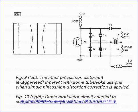
Some tube/yoke combinations have a scan -geometry characteristic such
that when the line scan current is modulated by a simple parabolic
waveform as described above the raster has inner pincushion distortion
as shown in Fig. 9.

Because
of this. the EW-correction system also has to modulate the S
-correction. Fig. 10 shows, in skeleton circuit form. how this can be
done. There are two coupling/S-correction capacitors. C3 and C3A. C3 is
the usual S -correction capacitor, but C3A has an increasing influence
as the diode modulator begins to have maximum effect towards the centre
of the screen. Critical choice of the value of C3A ensures that the
inner curved verticals shown in Fig. 9 are straightened out to give a
raster completely free from geometric distortion. Although all diode
modulators work on the same basic principle, in some designs a
transformer is used in place of the bridge coil to give better impedance
matching and balance. Fig. 11 shows such an arrangement, used by Bang
and Olufsen. The EW correction waveform is applied to transformer T6.
whose winding 1-2 takes the place of L2 in Figs. 8 and 10. This circuit
also provides inner -pincushion distortion correction as just described,
the supplementary S - correction capacitor being C36.
Diode Modulator Drive

The
parabolic EW drive waveform required is easily obtained by feeding the
field -scan sawtooth waveform to a double integrator. By adding a
sawtooth component the shape of the parabolic waveform can be tilted in
either direction to give keystone -distortion correction if required -
this is not generally necessary with modern tube/yoke designs. These EW
correction characteristics are adjustable by preset resistors or, in the
case of bus -programmable sets, remote control commands to the
deflection processor. Very often the EW modulator is used to correct the
previously mentioned picture breathing effect: this is done by feeding
to the EW modulator's control circuit a voltage that's proportional to
beam current.
BU208(A)
Silicon NPN
npn transistors,pnp transistors,transistors
Category: NPN Transistor, Transistor
MHz: <1 MHz
Amps: 5A
Volts: 1500V
HIGH VOLTAGE CAPABILITY
JEDEC TO-3 METAL CASE.
DESCRIPTION
The BU208A, BU508A and BU508AFI are
manufactured using Multiepitaxial Mesa
technology for cost-effective high performance
and use a Hollow Emitter structure to enhance
switching speeds.
APPLICATIONS:
* HORIZONTAL DEFLECTION FOR COLOUR TV With 110° or even 90° degree of deflection angle.
ABSOLUTE MAXIMUM RATINGS
Symbol Parameter Value Unit
VCES Collector-Emit ter Voltage (VBE = 0) 1500 V
VCEO Collector-Emit ter Voltage (IB = 0) 700 V
VEBO Emitter-Base Voltage (IC = 0) 10 V
IC Collector Current 8 A
ICM Collector Peak Current (tp < 5 ms) 15 A
TO - 3 TO - 218 ISOWATT218
Ptot Total Dissipation at Tc = 25 oC 150 125 50 W
Tstg Storage Temperature -65 to 175 -65 to 150 -65 to 150 oC
Tj Max. Operating Junction Temperature 175 150 150 °C
CRT TV EHT VOLTAGE MULTIPLIER - KASKADE COCKCROFT-WALTON CASCADE CIRCUIT FOR VOLTAGE MULTIPLICATION:
A
Cockcroft-Walton cascade circuit comprises an input voltage source and a
pumping and storage circuit with a series array of capacitors with
pumping and storage portions of the circuit being interconnected by
silicon rectifiers, constructed and arranged so that at least the
capacitor nearest the voltage source, and preferably one or more of the
next adjacent capacitors in the series array, have lower tendency to
internally discharge than the capacitors in the array more remote from
the voltage source.
1. An improved voltage multiplying circuit comprising,
2.
An improved voltage multiplying circuit in accordance with claim 1
wherein said first pumping capacitor is a self-healing impregnated
capacitor which is impregnated with a high voltage impregnant.
3.
An improved voltage multiplying circuit in accordance with claim 1
wherein said first pumping capacitor comprises a foil capacitor.
Description:
BACKGROUND OF THE INVENTION
The
invention relates in general to Cockcroft-Walton cascade circuits for
voltage multiplication and more particularly to such circuits with a
pumping circuit and a storage circuit composed of capacitors connected
in series, said pumping circuits and storage circuit being linked with
one another by a rectifier circuit whose rectifiers are preferably
silicon rectifiers, especially for a switching arrangement sensitive to
internal discharges of capacitors, and more especially a switching
arrangement containing transistors, and especially an image tube
switching arrangement.
Voltage multiplication cascades composed
of capacitors and rectifiers are used to produce high D.C. voltages from
sinusoidal or pulsed alternating voltages. All known voltage
multiplication cascades and voltage multipliers are designed to be
capacitance-symmetrical, i.e., all capacitors used have the same
capacitance. If U for example is the maximum value of an applied
alternating voltage, the input capacitor connected directly to the
alternating voltage source is charged to a D.C. voltage with a value U,
while all other capacitors are charged to the value of 2U. Therefore, a
total voltage can be obtained from the series-connected capacitors of a
capacitor array.
In voltage multipliers, internal resistance is
highly significant. In order to obtain high load currents on the D.C.
side, the emphasis in the prior art has been on constructing voltage
multipliers with internal resistances that are as low as possible.
Internal
resistance of voltage multipliers can be reduced by increasing the
capacitances of the individual capacitors by equal amounts. However, the
critical significance of size of the assembly in the practical
application of a voltage multiplier, limits the extent to which
capacitance of the individual capacitors can be increased as a practical
matter.
In television sets, especially color television sets,
voltage multiplication cascades are required whose internal resistance
is generally 400 to 500 kOhms. Thus far, it has been possible to achieve
this low internal resistance with small dimensions only by using
silicon diodes as rectifiers and metallized film capacitors as the
capacitors.
When silicon rectifiers are used to achieve low
internal resistance, their low forward resistance produces high peak
currents and therefore leads to problems involving the pulse resistance
of the capacitors. Metallized film capacitors are used because of space
requirements, i.e., in order to ensure that the assembly will have the
smallest possible dimensions, and also for cost reasons. These film
capacitors have a self-healing effect, in which the damage caused to the
capacitor by partial evaporation of the metal coating around the point
of puncture (pinhole), which develops as a result of internal
spark-overs, is cured again. This selfhealing effect is highly desirable
as far as the capacitors themselves are concerned, but is not without
its disadvantages as far as the other cirucit components are concerned,
especially the silicon rectifiers, the image tubes, and the components
which conduct the image tube voltage.
It is therefore an important object of the invention to improve voltage multiplication cascades of the type described above.
It is a further object of the invention to keep the size of the entire assembly small and the internal resistance low.
It is a further object of the invention to increase pulse resistance of the entire circuit.
It is a further object of the invention to avoid the above-described disadvantageous effects on adjacent elements.
It
is a further object of the invention to achieve multiples of the
foregoing objects and preferably all of them consistent with each other.
SUMMARY OF THE INVENTION
In
accordance with the invention, the foregoing objects are met by making
at least one of the capacitors in the pumping circuit, preferably
including the one which is adjacent to the input voltage source, one
which is less prone to internal discharges than any of the individual
capacitors in the storage circuit.
The Cockcroft-Walton cascade
circuit is not provided with identical capacitors. Instead, the
individual capacitors are arranged according to their loads and designed
in such a way that a higher pulse resistance is attained only in
certain capacitors. It can be shown that the load produced by the
voltage in all the capacitors in the multiplication circuit is
approximately the same. But the pulse currents of the capacitors as well
as their forward flow angles are different. In particular, the
capacitors of the pumping circuit are subjected to very high loads in a
pulsed mode. In the voltage multiplication cascade according to the
invention, these capacitors are arranged so that they exhibit fewer
internal discharges than the capacitors in the storage circuit.
The
external dimensions of the entire assembly would be unacceptably large
if one constructed the entire switching arrangement using such
capacitors.
The voltage multiplication cascade according to the invention also makes it possible to construct a reliably operating
arrangement
which has no tendency toward spark-overs, consistent with satisfactory
internal resistance of the voltage multiplication cascade and small
dimensions of the entire assembly. This avoids the above cited
disadvantages with respect to the particularly sensitive components in
the rest of the circuit and makes it possible to design voltage
multiplication cascades with silicon rectifiers, which are characterized
by long lifetimes. Hence, a voltage multiplication cascade has been
developed particularly for image tube circuits in television sets,
especially color television sets, and this cascade satisfies the highest
requirements in addition to having an average lifetime which in every
case is greater than that of the television set.
A further aspect
of the invention is that at least one of the capacitors that are less
prone to internal discharges is a capacitor which is impregnated with a
high-voltage impregnating substance, especially a high-voltage oil such
as polybutene or silicone oil, or mixtures thereof. In contrast to
capacitors made of metallized film which have not been impregnated, this
allows the discharge frequency due to internal discharges or
spark-overs to be reduced by a factor of 10 to 100.
According to a
further important aspect of the invention, at least one of the
capacitors that are less prone to internal discharges is either a foil
capacitor or a self-healing capacitor. In addition, the capacitor in the
pumping circuit which is adjacent to the voltage source input can be a
foil capacitor which has been impregnated in the manner described above,
while the next capacitor in the pumping circuit is a self-healing
capacitor impregnated in the same fashion.
Other objects,
features and advantages of the invention will be apparent from the
following detailed description of preferred embodiments, taken in
connection with the accompanying drawing, the single FIGURE of which:
BRIEF DESCRIPTION OF THE DRAWING
is a schematic diagram of a circuit made according to a preferred embodiment of the invention.
DETAILED DESCRIPTION OF PREFERRED EMBODIMENTS
The
voltage multiplier comprises capacitors C1 to C5 and rectifiers D1 to
D5 connected in a cascade. An alternating voltage source UE is connected
to terminals 1 and 2, said voltage source supplying for example a
pulsed alternating voltage. Capacitors C1 and C2 form the pumping
circuit while capacitors C3, C4 and C5 form the storage circuit.
In
the steady state, capacitor C1 is charged to the maximum value of the
alternating voltage UE as are the other capacitors C2 to C5. The desired
high D.C. voltage UA is picked off at terminals 3 and 4, said D.C.
voltage being composed of the D.C. voltages from capacitors C3 to C5.
Terminal 3 and terminal 2 are connected to one pole of the alternating
voltage source UE feeding the circuit, which can be at ground potential.
In the circuit described here, a D.C. voltage UA can be picked off
whose voltage value is approximately 3 times the maximum value of the
pulsed alternating voltage UE. By using more than five capacitors, a
correspondingly higher D.C. voltage can be obtained.
The
individual capacitors are discharged by disconnecting D.C. voltage UA.
However, they are constantly being recharged by the electrical energy
supplied by the alternating voltage source UE, so that the voltage
multiplier can be continuously charged on the output side.
According
to the invention, in this preferred embodiment, capacitor C1 and/or C2
in the pumping circuit are designed so that they have a lower tendency
toward internal discharges than any of the individual capacitors C3, C4
and C5 in the storage circuit.
It is evident that those skilled
in the art, once given the benefit of the foregoing disclosure, may now
make numerous other uses and modifications of, and departures from the
specific embodiments described herein without departing from the
inventive concepts. Consequently, the invention is to be construed as
embracing each and every novel feature and novel combination of features
present in, or possessed by, the apparatus and techniques herein
disclosed and limited solely by the scope and spirit of the appended
claims.
Inventors:Petrick, Paul (Landshut, DT)
Schwedler, Hans-peter (Landshut, DT)
Holzer, Alfred (Schonbrunn, DT)
ERNST ROEDERSTEIN SPEZIALFABRIK
US Patent References:
3714528 ELECTRICAL CAPACITOR WITH FILM-PAPER DIELECTRIC 1973-01-30 Vail
3699410 SELF-HEALING ELECTRICAL CONDENSER 1972-10-17 Maylandt
3463992 ELECTRICAL CAPACITOR SYSTEMS HAVING LONG-TERM STORAGE CHARACTERISTICS 1969-08-26 Solberg
3457478 WOUND FILM CAPACITORS 1969-07-22 Lehrer
3363156 Capacitor with a polyolefin dielectric 1968-01-09 Cox
2213199 Voltage multiplier 1940-09-03 Bouwers et al.


Chassis F6TT UNITS view.
- Luminance + Chrominance unit 492.045 G8 with TDA2500/3 + TDA2522 (all PHILIPS)
(Note the long luminance delay line)
- Synchronization Unit with TDA2593 (PHILIPS) 492.174 G10
- Sound - Audio Unit with TBA120U (Telefunken) + L130V (Fairchild Semiconductors) 492.044/E3
- RGB Amplifiers with TBA530 (PHILIPS) 943/K7
- Frame deflection unit 492.225/C1
- E/W Correction Unit 492.213/C
TDA2522 PAL TV CHROMA DEMODULATOR COMBINATION
FAIRCHILD LINEAR INTEGRATED CIRCUIT
GENERAL DESCRIPTION- The TDA2522 is a monolithic integrated circuit designed as
a synchronous demodulator for PAL color television receivers. It includes an 8,8 MHz

oscillator and divider to generate two 4.4 MHz reference signals and provides color difference outputs.
PACKAGE OUTLINE 9B
The
TDA2522 is Intended to Interface directly with the TDA2560 with a
minimum oF external components. The TDA2530 may be added if RGB drive is
required. The TDA2522
is constructed using the Fairchild Planar* process.
TDA2520 COLOUR DEMODULATOR COMBINATION
The TDA2520 is an integrated synchronous demodulator combination for colour television
receivers incorporating the following functions :

~ 8, 8 MHZ oscillator followed by a divider giving two 4, 4 MHZ signals used as reference
signals
- keyed burst phase detector for optimum noise behaviour
- a stage to obtain chrominance signal control (a. c. c.) and an a. c. c. reference level
- a colour killer and identification signal detector
- two synchronous demodulators for the (B-Y) and (R-Y) signals
- temperature compensated emitter follower outputs
- PAL switch
- PAL flip-flop
- integrated capacitors in the symmetrical demodulators reduce unwanted carrier-
signals at the outputs.
TDA2593 SYNCHRO AND HORIZONTAL DEFLECTION CONTROL FOR COLOR TV SETDESCRIPTION
The TDA2593 isa circuit intended for the horizontal
deflectionof color TVsets, suppliedwith transistors
or SCR’S.
.LINE OSCILLATOR(two levels switching)
.PHASE COMPARISON BETWEEN SYNCHRO-
PULSE AND OSCILLATOR VOLTAGE
Ø 1, ENABLED BY AN INTERNAL PULSE,
(better parasitic immunity)
.PHASE COMPARISON BETWEEN THE FLYBACK
PULSES AND THE OSCILLATORVOLTAGE
Ø2
.COINCIDENCE DETECTOR PROVIDING A
LARGE HOLD-IN-RANGE .FILTER CHARACTERISTICS AND GATE
SWITCHING FOR VIDEO RECORDER APPLICATION
.NOISE GATED SYNCHRO SEPARATOR
.FRAME PULSE SEPARATOR
.BLANKING AND SAND CASTLE OUTPUT
PULSES
.HORIZONTAL POWER STAGE PHASE LAGGING
CIRCUIT
.SWITCHING OF CONTROL OUTPUT PULSE
WIDTH
.SEPARATED SUPPLY VOLTAGE OUTPUT
STAGE ALLOWING DIRECT DRIVE OF
SCR’S CIRCUIT .SECURITY CIRCUIT MAKES THE OUTPUT
PULSE SUPPRESSED WHEN LOW SUPPLY
VOLTAGE.

NORDMENDE SPECTRA COLOR SC1032 CHASSIS F6TT COLOR AMPLIFIER WITH Constant bandwidth RGB output amplifiers having simultaneous gain and DC output voltage control :
A
color television receiver includes conventional circuitry for
processing and detecting a received color television signal. Three
chrominance-luminance matrices combine detected color difference and
luminance signals forming color red, blue and green video signals.
Emitter follower coupling stages apply the color video signals
individually to each
of three output amplifiers which in turn drive the cathode electrodes
of a unitized gun CRT. Potentiometers couple the emitter electrodes of
the output amplifiers to a source of operating potential providing a
simultaneous signal gain and DC output voltage adjustment for each
amplifier during CRT color temperature setup. A voltage divider controls
the voltage applied to the common screen grid electrode of the CRT
providing a master setup adjustment.
1. In a color
televison receiver, for processing and displaying a received television
signal bearing modulation components of picture information, having a
cathode ray tube including a trio of electron source means producing
individual electron beams impinging an image screen to form three
substantially overlying images and in which the respective operating
points and relative conduction levels of said electron source means
determine the color temperature of the reproduced image, the
combination comprising:
master conduction means, coupled to said trio of electron source means simultaneously varying said conduction levels;
a
plurality of substantially equal bandwidth amplifiers, each coupled
to a different one of said electron source means, separately
influencing said conduction levels;
low output impedance signal
translation means recovering said picture information and supplying
it to each of said plurality of amplifiers; and
separate
adjusting means individually coupled to at least two of said
amplifiers for simultaneously producing predetermined same sense
variations in gain and DC output voltage of its associated amplifier
while preserving said bandwidths.
2. The combination set forth in
claim 1, wherein the transconductance and cutoff voltage of each of
said electron source means bear a predetermined relationship and
wherein said simultaneous predetermined variations in gain and DC
output voltage are determined by said transconductance-cutoff voltage
relationship. 3. The combination
set forth in claim 2, wherein said plurality of amplifiers each
include a gain and DC output voltage determining impedance and wherein
each of said separate adjusting means include:
a variable
impedance, coupling said gain and DC output voltage determining
impedance of said associated amplifier to a source of bias current and
forming a shunt path for signals within said amplifier.
4. The
combination set forth in claim 3, wherein each of said electron source
means include a cathode electrode and wherein each of said amplifiers
include:
a transistor having input, common, and output
electrodes, said output electrode being coupled to said electron
source means cathode.
5. The combination set forth in claim 4,
wherein said gain and DC output voltage determining impedance is
coupled to said common electrode.
6. The combination set forth in claim 5, wherein said input, common,
and output electrodes of said transistors are defined by base,
emitter, and collector electrodes, respectively.
7. The combination set forth in claim 6, wherein said
gain and DC output voltage determining impedance includes a resistor
coupling said emitter electrode to ground and wherein said variable
impedance includes:
a resistive control, having a variable resistance, coupling said emitter electrode to a source of operating potential.
8.
The combination set forth in claim 7, wherein said three electron
source means include control grid and screen grid electrodes common to
said three electron guns and wherein variations of cathode electrode
voltages permit changes of said relative conduction levels and said
respective operating points. 9.
The combination set forth in claim 8, wherein said master conduction
means includes a variable bias potential source coupled to said common
screen grid electrode.
Description:
BACKGROUND OF THE INVENTION
This
invention relates to color television receivers and in particular to
cathode ray tubes (CRT) drive systems therefor. Each of the several
types of color television cathode ray tubes in current use includes a
trio of individual electron sources producing distinct electron beams
which are directed toward an image screen formed by areas of
colored-light-emitting phosphors deposited on the inner surface of the
CRT. The phosphors emit light of a given additive primary color (red,
blue or green) when struck by high energy electrons. A "delta" electron
gun arrangement, in which the electron sources comprise three
electron guns disposed at the vertice
s
of an equilateral triangle, having its base oriented in a horizontal
plane and its apex above or below the base plane, may be used.
Alternatively, the three electron sources may be "in line", that is,
positioned in a horizontal line. In either case, the three beams
produced are subjected to deflection fields and scan the image screen
in both the horizontal and vertical directions thereby forming three
substantially overlying rasters.
The phosphor deposits forming
the image screen may alternatively comprise round dots, elongated
areas, or uninterrupted vertical lines. A parallax barrier or shadow
mask, defining apertures generally corresponding to the shape of the
phosphor areas, is interposed between the electron guns and the image
screen to "shadow" or block each phosphor area from electrons emitted
from all but its corresponding electron gun.
A color television
signal includes both luminance (monochrome) and chrominance (color)
picture components. In the commonly used RGB drive systems the
separately processed luminance and chrominance information is matrixed
(or combined) before application to the CRT cathodes. Three output
amplifiers apply the respective red, blue and green video signals thus
produced for controlling the respective electron source currents.
The
luminance components have substantially the same effect on all three
electron sources whereas the color components are differential in
nature, causing relative changes in electron source currents. In the
absence of video signals, the combined raster should be a shade of grey.
At high gun currents, the grey is very near white and at low
settings, it is near black. The "color", commonly called color
temperature, of the monochrome raster depends upon the relative
contributions of red, blue and green light. At high color
temperatures, the raster may appear blue and at low color temperatures
it may appear sepia. While the most pleasing color temperature is
largely a matter of design preference, ideally the receiver should not
change color temperature under high and low brightness nor for high
and low frequency picture information.
Generally, the electron
sources comprise individual electron guns each including separately
adjustable cathode, control grid and screen grid electrodes and a
desired color temperature is achieved by adjustment of each electrode
voltage during black and white setup. While the exact setup procedure
employed varies with the manufacturer and specific CRT configuration,
all manufacturers attempt to achieve consistent color temperature
throughout the usable range of CRT beam current variations.
A typical color temperature adjustment involves setting the low light color temperature condition of each electron gun by adju

sting
its screen grid electrode voltage to produce the required DC
conditions between electron guns at minimum beam currents. A high light
or dive adjustment at increased CRT beam current is then made to
insure consistent color temperature. In receivers utilizing CRT's with
separately adjustable screen grid electrode voltages, the drive
adjustment may take the form of a minor change in signal gain of the
output amplifiers. The process is, in essence, one of configuring the
operating points of the three electron guns to conform to three
substantially identical output amplifiers.
The recently
developed economical "unitized gun" type CRT has a combined electron
source structure in which three common control grids and three common
screen grids are used with the cathodes being the only electrically
separate electrodes. The greatly simplified and more economical
unitized gun structure, however, imposes some restrictions on the
circuitry used to drive the electron sources. Perhaps most significant
is the absence of
the
flexibility previously provided by individually adjustable screen
grid electrode voltages. Due in part to the inverse relationship
between electron source transconductance, which may be thought of as
"gain" of the electron source, and cutoff voltage, the typical
individual low level color temperature or equal cutoff adjustment
described above also performs the additional function of establishing
nearly equal transconductances for the three electron sources. As a
result only minor relative changes in electron source currents occur
at higher CRT beam currents.
Color temperature adjustment in a
receiver with a unitized gun CRT involves a somewhat different
process, namely, configuring the drive and bias applied to each of the
gun cathodes to accommodate differences in relative electron source
characteristics which, without the equalizing effect of separate
screen electrode adjustments, may be considerable.
Initially
television receivers using unitized gun CRT's utilized a variable DC
voltage divider operative upon each output amplifier to provide
adjustment of the DC cutoff voltage. Drive, or signal gain, adjustment
to accommodate differences in electron source transconductances was
generally accomplished by separate individual gain controls operative
on each of the output amplifiers.
However, the more recently
developed unitized gun systems combine the DC voltage (cutoff) and
signal gain (drive) adjustments for each electron source by
simultaneously varying the signal gain and DC voltage in the same
direction in a predetermined relationship. One such system used three
CRT coupling networks each of which includes a variable impedance
simultaneously operative on both the amplitude of coupled signal and DC
voltage. Another system uses a variable collector load impedance for
each of the output amplifiers, making use of the changes in amplifier
signal gain and DC output voltage resulting from collector load
variations.
While such systems provide an adequate range of
adjustment to achieve color temperature setup using a reduced number of
controls, they often degrade image quality. Ideally, the luminance
portion of the signal is applied uniformly to each of the three
electron sources. Although the relative signal amplitudes may be
varied to accommodate transconductance differences between electron
sources, it is desirable that each applied signal be an otherwise
identical replica of the others. The variable impedance elements in
the voltage divider networks and variable collector loads of the prior
art interact with the capacities inherent in the output amplifiers
and electron gun structures to produce unequal bandwidths for the
different color video signals, which cause color changes in their high
frequency components (which correspond to detailed picture
information). The resulting effect upon the displayed image is similar
in appearance to the well-known "color fringing" or misconvergence
effect.
OBJECTS OF THE INVENTION
It is an object of the present invention to provide an improved color television receiver.
It is a further object of this invention to provide a novel CRT color temperature setup system.
SUMMARY OF THE INVENTION
In
a color television receiver, for processing and displaying a received
television signal bearing modulation components of picture
information, a
cathode
ray tube includes three electron source means producing individual
electron beams which impinge an image screen to form three
substantially overlying images. The respective operating points and
relative conduction levels of the electron source means determine the
color temperature of the reproduced image. Master conduction means,
coupled to the three electron source means, simultaneously vary the
conduction levels and a plurality of substantially equal bandwidth
amplifiers, each coupled to a different one of the electron source
means, separately influence the conduction levels. Low output impedance
signal translation means recover the picture information and supply it
to each of the amplifiers. Separate adjusting means are individually
coupled to at least two of the amplifiers for simultaneously producing
predetermined variations in the gain and DC output voltage of the
amplifiers while preserving the bandwidths.
BRIEF DESCRIPTION OF THE DRAWING
The
drawing shows a partial-schematic, partial-block diagram
representation of a color television receiver constructed in accordance
with the present invention.
DESCRIPTION OF THE PREFERRED EMBODIMENT
Referring
to the drawing, a signal processor 10 includes conventional circuitry
(not shown) for amplifying a received television signal and detecting
the
modulated components of luminance and chrominance information therein.
The output of signal processor 10 is coupled to a luminance amplifier
11 and a chrominance processor 30. Luminance amplifier 11 is
conventional and includes circuitry controlling brightness and contrast
of the luminance signal. The output of luminance amplifier 11 is
coupled to three luminance-chrominance matrices 12, 13 and 14.
Chrominance processor 30 includes conventional chrominance information
detection circuitry for providing three color difference or
color-minus-luminance output signals (R-Y, G-Y and B-Y) which are
individually coupled to luminance-chrominance matrices 12, 13 and 14,
respectively. The signal from luminance amplifier 11 is combined with
the color-minus-luminance signals from chrominance processor 30 to form
the respective red, green and blue video signals which are coupled to
the R, G and B output amplifiers 15, 16 and 17, respectively. The
outputs of amplifiers 15, 16 and 17 are coupled to the cathode
electrodes 23, 24 and 25, respectively, of a CRT 20 having an image
screen 21. A voltage divider, formed by a series combination of
resistors 83 and 84, is coupled between a source of operating potential
+V
2 and ground. The junction of resistors 83 and 84 is
connected to a common control grid electrode 28 and to ground by a
filter capacitor 85 which provides a signal bypass. A potentiometer 80
and a resistor 81 are series coupled between a source of operating
potential +V
1 and ground, forming another voltage divider.
The junction of potentiometer 80 and resistor 81 is connected to common
screen grid electrode 29 and to ground by a bypass capacitor 82.
Cathode electrodes 23-25, control grid electrode 28 and screen grid
electrode 29 are part of a unitized gun structure in CRT 20 with the
control grid and screen grid being common to each of the three electron
sources defined by the separate cathode electrodes.
While
luminance-chrominance matrices 12 and 13 are shown in block form, it
should be understood that they are identical to the detailed structure
of matrix 14. Similarly, red output amplifier 15 and green output
amplifier 16 are identical to the detailed structure of blue output
amplifier 17. Further, the receiver shown is understood to include
conventional circuitry for horizontal and vertical electron beam
deflection together with means deriving a CRT high voltage accelerating
potential, all of which have, for clarity, been omitted from the
drawing.
Luminance-chrominance matrix 14 includes a matrix
transistor 40 having an emitter electrode 41 coupled to ground by a
resistor 55 and by a series combination of resistors 46 and 47, a base
electrode 42 coupled to the output of luminance amplifier 11, and a
collector electrode 43 coupled to a source of operating potential +V
3 by a resistor 45. The B-Y output of chroma processor 30 is connected to the junction of resistors 46 and 47. An emitte
r-follower
transistor 50 has an emitter electrode 51 coupled to ground by a
resistor 56, a base electrode 52 connected to the collector of matrix
transistor 40, and a collector electrode 53 connected to +V
3.
Blue
amplifier 17 includes an output transistor 60 having an emitter
electrode 61 coupled to ground by a series combination of resistors 67
and 68, a base electrode 62 connected to the emitter of transistor 50,
and a collector electrode 63 coupled to +V
2 by a resistor 66.
A series combination of a potentiometer 70 and a resistor 69 couples
the junction of resistors 67 and 68 to +V
3. Collector 63, which is the output of amplifer 17, is connected to cathode 25 of CRT 20.
During
signal reception, the separately processed luminance and B-Y color
difference signals are applied to matrix transistor 40. The combi
ned
signal developed at its collector 43 forms the blue video signal which
controls the blue electron beam in CRT 20 and represents the relative
contribution of blue light in the image produced.
The blue video
signal at collector 43 is coupled via transistor 50 to base 62 of
output transistor 60. The low source impedance of emitter follower
transistor 50 obviates any detrimental effects upon the blue video
signal due to loading at the input to amplifier 17 caused by gain or
frequency dependent input impedance variations of amplifier 17. The
blue video signal applied to base 62 is amplified by transistor 60 to a
level sufficient to control the conduction of its respective electron
source.
During color temperature setup, a predetermined setup
voltage (corresponding to black) is applied to matrices 12, 13 and 14.
The voltage on common screen grid electrode 29 is adjusted, by varying
potentiometer 80 which together with resistor 81 and capacitor 82 form
master conduction means, to cause a low brightness raster to appear on
image screen 21. As will be seen, adjustment of potentiometer 70 and
the corresponding potentiometers in amplifiers 15 and 16 establish the
correct combination of DC electron source cathode voltages and output
amplifier gains to produce the selected color temperature at both low
and high CRT beam currents.
Amplifier 17 includes a common
emitter transistor stage in which the impedance coupled to emitter
electrode 6 is a gain and DC output voltage determining impedance.
Signal gain is approximately equal to the ratio of the collector
impedance (resistor 66), to this gain and DC voltage determining
impedance (ignoring the effects of capacities associated with the tr
ansistor and the electron gun which will be considered later). Because the source of operating potential +V
3
coupled to potentiometer 70 forms a good AC or signal ground, the
series combination of resistor 69 and potentiometer 70 are effectively
in parallel with resistor 68 and the total impedance coupling emitter 61
to signal ground comprises resistor 67 in series with this combination
of resistors 68 and 69 and potentiometer 70. Variations in this
impedance caused by adjustment of potentiometer 70 changes the ratio of
collector to emitter impedances and thereby the gain of amplifier 17.
If potentiometer 70 is varied to present increased resistance, gain is
reduced and if varied to present decreased resistance, gain is
increased.
The DC voltage at collector 63 of transistor 60 is
determined by the product of the collector resistance and quiescent
collector current (current in the absence of applied signal) and V
2.
The voltage at base 62 is established by the emitter voltage of
transistor 50. Variations in the resistance of potentiometer 70 cause
variations in current flow in the series path including potentiometer 70
and resistors 69 and 68. The voltage developed across resistor 68 is
supplied to emitter 61 through resistor 67.
In the absence of
signal, the DC voltage at base 62 is constant and the relative voltage
between base 62 and emitter 61, which controls the conduction level of
transistor 60, is a function of the voltage at emitter 61. Increases in
the resistance of potentiometer 70 reduce the emitter voltage, increase
the relative base-emitter voltage of transistor 60, and increase
collector current. The increased collector current develops a greater
voltage drop across collector resistor 66 and reduces the DC voltage at
collector 63 (and cathode 25). Conversely, a decrease in the resistance
of potentiometer 70 increases the voltage at emitter 61, reducing the
relative base-emitter voltage and decreasing collector current. The
smaller voltage drop across resistor 66 increases the DC voltage at
collector 63 and cathode 25.
Thus, increasing the resistance
of
potentiometer 70 produces proportionate simultaneous reduction of the
DC voltage applied to cathode 25 and the voltage gain of amplifier 17,
whereas decreasing the resistance of potentiometer 70 produces
proportionate simultaneous increase of the DC voltage and signal gain.
As mentioned above, amplifiers 15 and 16 are identical to amplifier 17.
In practice only two of the three output amplifiers require adjustment
to achieve color temperature setup. However, greater flexibility and
optimum use of amplifier signal handling capability is realized if all
three output amplifiers are adjustable.
As previously mentioned
capacities associated with transistor 60, cathode 25 and corresponding
interconnections (such as those used to couple collector 63 to cathode
25) are effectively in parallel with collector load resistor 66 forming a
partially reactive "coupling network" which exhibits a frequency
characteristic (bandwidth) affecting signals coupled therethrough. In
practice, the other coupling networks have identical bandwidths and
affect their signals in an equal manner. The setup control adjustments
of the present invention do not change the characteristics of these
coupling networks and the uniformity of signal coupling for the
different color signals is preserved. In contrast, conventional
adjustment circuitry (whether variable collector load or voltage
divider) place variable impedances within these couplings. The varied
adjustments of these impedances to effect color temperature control
adjustment disturb the bandwidth characteristics of the coupling
networks causing differential variations in the individual color video
signals.
What has been shown is an RGB CRT drive system which
includes output amplifiers each having a single control which
simultaneously achieves changes of the DC
output voltage and signal gain of the amplifier in a predetermined
relationship. The bandwidths of all three output amplifiers and their
associated coupling networks remain substantially undisturbed by these
control adjustments during CRT color temperature setup.
While
particular embodiments of the invention have been shown and described,
it will be obvious to those skilled in the art that changes and
modifications may be made without departing from the invention in its
broader aspects, and, therefore, the aim in the appended claims is to
cover all such changes and modifications as fall within the true spirit
and scope of the invention.


The new colour picture tube introduced in the UK by Thorn and developed in the US by RCA has an abundance of novel features designed to make it easier to operate and perhaps cheaper to produce. It arrives in an aura of snappy abbreviations such as PST ("precision static toroid") and ITC ("integral tube components") but the proud inventors for some reason insist on giving its full name, Precision In - Line System, the full treatment on each appearance. It seems inevitable that others will have no such inhibitions, so we shall draw comparisons between the new PI tube, the standard shadowmask tube and the Sony Trinitron. These are the only colour large scale production at present. Over twenty years have passed since RCA introduced the shadowmask cathode-ray tube, the first colour television display device to be mass produced. For most of this time it has remained the only colour picture tube available and it is now prodUced under licence to the inventors by many manufacturers all over the world. Detail improvements have been made of course but the basic scheme has remained unchanged: three electron guns in a triangular (or "delta") formation, a shadowmask etched with a pattern of tiny holes and a corresponding array of red, green and blue phosphor dots on the screen. In the last few years the Sony Trinitron has appeared and soon established itself as a display device for use in the small screen portable receivers for which it was designed. The three electron guns in this tube are closely spaced side by side in a horizontal plane. The "shadowmask" contains vertical slits instead of holes and the screen is composed of vertical phosphor stripes in a red -green- blue sequence.

 (1885-1940) in Dresden. Following the destruction of the plant during the bombing raids in 1945, Martin Mende (the founder's son) created a new company in Bremen in 1947, in a former Focke-Wulf plant, under the name North German Mende Broadcast GmbH.
The name was subsequently changed to Nordmende: subsequently the
company became one of the prominent German manufacturers of radios,
televisions, tape recorders and record players in the 1950s and 1960s.
(1885-1940) in Dresden. Following the destruction of the plant during the bombing raids in 1945, Martin Mende (the founder's son) created a new company in Bremen in 1947, in a former Focke-Wulf plant, under the name North German Mende Broadcast GmbH.
The name was subsequently changed to Nordmende: subsequently the
company became one of the prominent German manufacturers of radios,
televisions, tape recorders and record players in the 1950s and 1960s.
 Nordmende
was well known for its televisions throughout Ireland during the
1970s and 1980s, the company bought the rights to the name and
launched a range of white goods including fridges, freezers, washing machines, and dishwashers, alongside a revamped range of flat-screen TVs and stereos.
Nordmende
was well known for its televisions throughout Ireland during the
1970s and 1980s, the company bought the rights to the name and
launched a range of white goods including fridges, freezers, washing machines, and dishwashers, alongside a revamped range of flat-screen TVs and stereos. otalverlust in
Dresden gründet Martin Mende (30.12.1898-1982) unter Mitwirkung von
Hermann Weber am 26. August 1947 [FT5901] in Bremen-Hemelingen die
Norddeutsche Mende-Rundfunk GmbH.
otalverlust in
Dresden gründet Martin Mende (30.12.1898-1982) unter Mitwirkung von
Hermann Weber am 26. August 1947 [FT5901] in Bremen-Hemelingen die
Norddeutsche Mende-Rundfunk GmbH. Auch Konzertschränke
scheinen Ende der 50er bis Anfang 60er Jahre eine tragende Säule für
Nordmende zu sein. Dabei verwendet die Firma immer wieder gleiche Namen
wie «Cabinet», «Caruso», «Casino», «Cosima» sowie «Arabella» und
«Isobella» mit wechselnden Zusatz-Nummern oder den Zusatz «Stereo», z.B.
in den Jahren 1959 und 1960/61.
Auch Konzertschränke
scheinen Ende der 50er bis Anfang 60er Jahre eine tragende Säule für
Nordmende zu sein. Dabei verwendet die Firma immer wieder gleiche Namen
wie «Cabinet», «Caruso», «Casino», «Cosima» sowie «Arabella» und
«Isobella» mit wechselnden Zusatz-Nummern oder den Zusatz «Stereo», z.B.
in den Jahren 1959 und 1960/61. Commons: Nordmende – Sammlung von Bildern, Videos und Audiodateien