


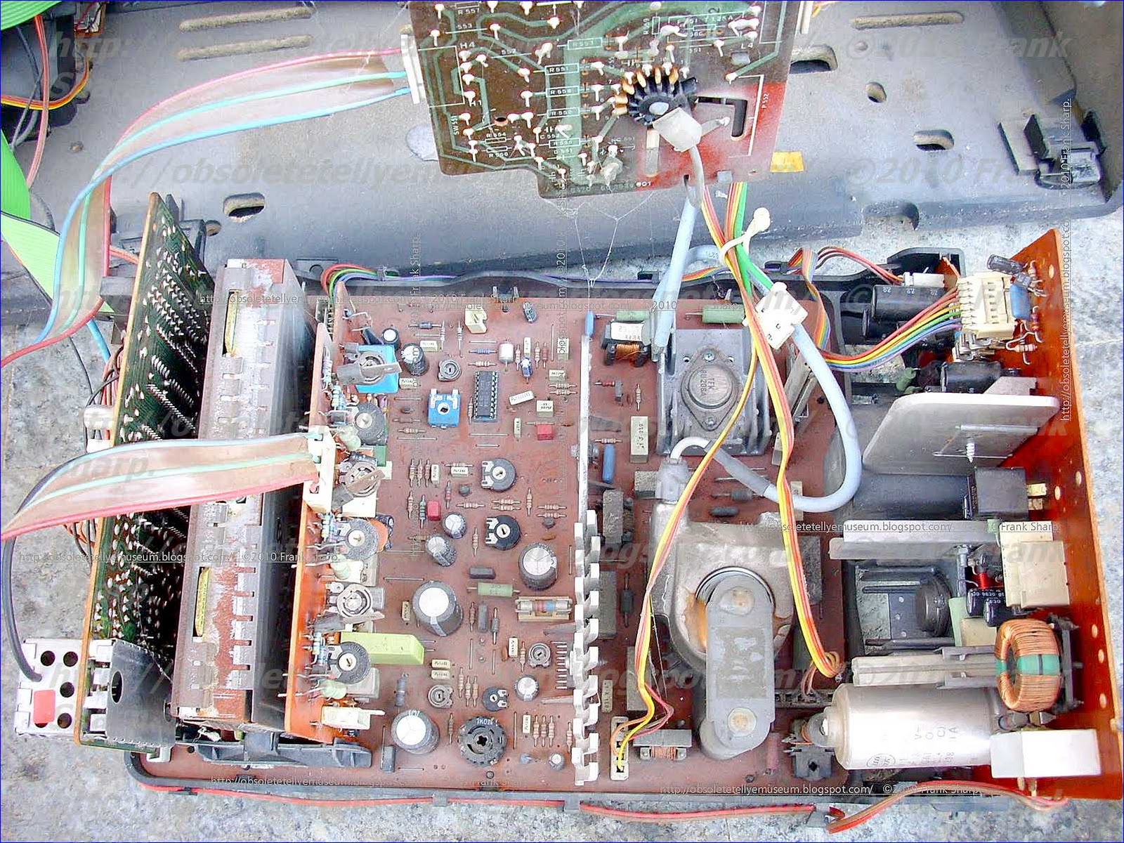
The LUXOR 5134 TYPE 18051341 CHASSIS B3-1 (SX9) was first monocarrier horizontal placed chassis from this firm and was first introducing several features in one board pcb.
TDA3301 -- COLOR PROCESSOR
TDA4290 -- TONE CONTROL
TDA2594 -- SYNC
TDA4427 -- VIDEO IF AMPLIFIER
SAB3035 -- CITAC
TDA1670 -- FRAME DEFLECTION AMPL.
TDA4600 -- POWER SUPPLY
LUXOR CHASSIS B3-1 (SX9) :
 The SX9 is essentially a single -board design (the p.c.b. measures 14in. by 9in.) which of course is designed to facilitate automatic insertion of components, and incorporates frequency synthesis tuning as standard. A block diagram of the receiver is shown in Fig. 1. Starting with the power supply, this is a self -oscillating switch -mode type based on the Siemens design but incorporating the Siemens TDA4600 i.c. providing base current control to a BU208 transistor.
The most important difference is that the Luxor SX9 uses a mains isolated version. There are two versions of the line output stage: one suitable for 90° c.r.t.s and another for 110°. The 90° type uses a diode -split transformer which provides 24kV of e.h.t. The 110° type uses a conventional transformer/ tripler combination and provides 25kV e.h.t. The most interesting aspect is the use of a 110° deflection tube with a pincushion -distortion free yoke. This is the first time that we have seen this type of tube in use. It obviates the need for the usual diode modulator, and width control is provided by a simple adjustable coil in series with the line scan coils as in the 90° version. Vertical deflection is taken car
e of by an SGS-Ates i.c. type TDA1670. This is a development of the well known TDA1170 but housed in a higher power vertically - mounted pack, and offers greater output stage current capability with thermal shutdown protection and an extended blanking pulse generator which effectively suppresses all non -active lines, including the teletext lines. The sync generator/line oscillator uses a PHILIPS TDA2594 which is a later generation PHILIPS TDA2593 with the exception that it offers sound mute when the oscillator is not locked by incoming sync (e.g. when the receiver is not tuned to a station). This feature is a legal requirement for new receivers in some countries, W. Germany for example, and we are going to encounter it frequently from now on.Turning to the signals side, the chassis uses a combined v.h.f./u.h.f. tuner as standard. The tuner has an integral +256 prescaler i.c. which provides the necessary local oscillator signal for the frequency synthesis tuning section. The if output from the tuner is amplified by a Plessey SL1431 i.c. which provides an a.g.c. signal for the tuner without the need for the usual a.g.c. takeover point preset. This i.c. provides a balanced output which drives a Surface Acoustic Wave Filter.
The filter is unusual in that it has two balanced outputs whose bandpass characteristics are different. The vision carrier output has the sound carrier suppressed more than usual, resulting in fewer unwanted interference effects, e.g. sound-chroma beats. This is fed to a TELEFUNKEN TDA4427 i.c. which performs similar functions to the better known PHILIPS TDA2540, i.e. vision if amplification and detection and a.f.c. detection. It differs from the TDA2540 in that it offers two video output signals of opposite polarity.
The sound carrier output from the SAWF is passed to a TDA4282 i.c. for processing. A block diagram is shown in Fig. 2. The i.c. has two basic sections.
 The first is similar to a standard vision LE amplifier and detector. The i.f. amplifier incorporates a.g.c. control; the detector uses a standard LC tuned circuit and produces an output very similar to a standard composite video signal. This is brought out of the i.c. and the 6MHz sound i.f. signal is extracted by the usual 6MHz ceramic filter. This signal is fed back into the second section of the i.c. which com- prises an i.f. amplifier and detector, the latter using a ceramic discriminator and therefore not requiring any adjustment.
The recovered audio signal is routed through a "VCR" switching block inside the i.c. This enables either the off -air signal to pass to the output buffer amplifier or, by applying a switching voltage to the i.c., it blocks the off -air signal and allows an external audio signal to be connected to the buffer. In order to minimise the number of pins on the i.c. and to reduce the switching complexity, a single pin is used to provide an off -air audio output signal via the SCART socket to, say, a VCR in the record mode. When the switching voltage to the i.c. is applied, this same pin reverts to an input pin which will accept an external audio signal (e.g. from a VCR in the playback mode) and route it via the buffer stage to the TV set's audio amplifier. The audio output from the i.c. proceeds to a TDA4290 i.c. which provides d.c. operated control of volume, bass and treble. The output from this i.c. is fed to a TDA2008 a.f. amplifier and then to a speaker and earphone socket. In its standard form the chassis offers only mono reproduction: it's easy to convert for stereo by substituting the audio control/output section for one containing an additional TDA4290 and a twin a.f. amplifier i.c. Meanwhile, back at the composite video output from the TDA4427, this is passed through a 6MHz ceramic trap (again, no adjustment) to remove any residual intercamer sound signal present on the video signal and then, after some switching to enable video out/video in, the selected video signal is processed by a Motorola TDA3301 single -chip colour decoder. This is virtually identical to the TDA3300 which has been described in previous posts on Obsolete Technology Tellye ! .
There is nothing particularly exceptional about the i.c. (except the extraordinary degree of integration) - it offers the usual RGB inputs with fast picture blanking, making an easy interface with the optional teletext decoder module.One nice feature of this i.c. is the facility of automatic black level control. It does this by monitoring beam current during flyback blanking.
The value of the beam current under these conditions should of course be zero (i.e. the tube be cut off or else you don't have blanking!). If the i.c. senses some beam current on any one of the three guns, then it adjusts the d.c. pedestal of the appropriate colour output until there is zero beam current.
Not only does this process result in "perfect" grey scale but it retains this throughout the life of the tube (as tubes age the black level for any of the three guns can change causing a deterioration of grey scale). It also compensates for component value changes in the video output stages due to age. The video output stages themselves are of the class AB type and, as is usual nowadays, mounted on thetube base board to avoid the extra capacitance offered by the RGB connecting cable required with mounting on the main p.c.b. An extra pnp transistor connected between each video output stage and the c.r.t. cathode senses the beam current and feeds the information back to the colour decoder i.c. as explained above.
Digital Control:So much then for the basic outline of the receiver. We now turn our attention to the digital sectionwhich contains the frequency synthesis tuning system. The SX9's control system is based on a Philips/Mullard development which offers: (1) user controls - either by remote plus local or local only; (2) tuning; (3) teletext acquisition and display (optional); and (4) signal processing control. It is a very versatile and sophisticated system, and the high degree of integration means that few peripheral components are needed. The system is illustrated in Fig. 3.
It is based on five i.c.s: PHILIPS MAB8440 microcomputer; PHILIPS SAA3004 remote control transmitter; TDA3048 infra -red preamplifier; PCD8571 CMOS memory; and PHILIPS SAB3035 tuning i.c.
Remote Control:
The remote control transmitter is very straightforward. The keypad is the usual matrix type. The i.c. is capable of a maximum of 7 sets of 64 commandsalthough of course not all are used in the SX9.
Instead of the usual expensive crystal, the PHILIPS SAA3004 uses a 455kHz ceramic resonator to produce its internal clock. In order to conserve battery power, the oscillator is not active until a button is depressed. In this standby condition the i.c. consumes a mere 2µA.
The output from the i.c. is amplified by a single transistor and the output from this is used to drive an i.r. diode. Very few peripheral components are used. The remote control commands are pulse -position coded, with modulated pulses. The spacing between the frequency bursts determines whether thesignal is a "0" or a "1". Frequency bursts allow the use of a narrow band receiver circuit which makes the system less sensitive to interference. A complete command consists of a reference bit, a toggle bit, 3 address bits and 6 bits
for the command itself. Incidentally, if a command button is pressed for sufficiently long to enable the transmitter to start sending 130 the information, but happens to be released before the process is completed, the transmitter will ensure that the complete command is sent before returning to its standby mode. The reference bit is used by the receiver as a time reference - it is always a "1" and lasts for 7.59ms. The toggle bit changes state each time a new command is sent. The address bits are selected by the manufacturer to suit each application. Their selection determines which one out of the possible 7 sets of commands is to be used. In the SX9, the address bits are all "0". The six command bits are dependent on the command itself and of course allow one of 64 commands to be sent. At the receiver end, the TDA3048 infra -red receiver i.c. consists of a controlled r.f. amplifier, demodulator, a.g.c. generator, limiter, pulse shaper and output stage. A filter at the input of the i.c. limits the bandwidth of the applied signal, thus ensuring minimum interference. A "Q -killer" circuit automatically reduces the Q of the input tuned circuit in order to limit strong signals reaching the amplifier. This can happen if the transmitter is operated too close to the receiver, in which case the signal can exceed the a.g.c. range. Microcomputer Control System The heart of the system is the microcomputer. Most of its functions are already programmed, but the customer (TV manufacturer) has a number of options he can specify. It is therefore best described as a dedicated microcomputer (designed specifically for this sort of application) whose parameters can be altered by software control. Its tasks are to decode the remote control com- mands, offer local customer "front panel" control, generate data for a seven segment display, control the tuning i.c. and communicate with other devices connected to the serial bus (i.e. memory, text, etc.). The modulated pulse train from the infra -red receiver module is connected to the microcomputer where it is decoded. This function is performed by a block known as the control/timing block. It incorporates the microcomputer's on chip oscillator which runs at 4MHz. In order to store data when the set is switched off, a 1k memory powered by a rechargeable NiCad 1.2V battery is used. The PCD8571 is a 1024 bit CMOS memory organised as 128 x 8 bits. It is connected to the microcomputer via the serial bus. The memory stores channel number; frequency offset from "correct" channel frequency; TV standards (for use in multistandard sets); long/short time constant; on off satellite; on -off video; on - off a.f.c.; on -off NTSC; preferred teletext pages; seven personal preference adjustments (e.g. volume, brightness, etc.). The above render the memory virtually full. The memory is powered from the +5V rail via a diode when the set is switched on. At the same time, the battery is charged via a current limiting resistor. When the +5V collapses (i.e. when the set is switched off), the diode is reversed biased, therefore preventing the battery from being discharged by other circuitry connected to the +5V rail. The last i.c. in the system is the tuning i.c., type SAB3035. This provides synthesised tuning with a.f.c.; band switching; reception switching (e.g. satellite and VCR); analogue control of up to 8 functions. It receives its information from the microcomputer via the serial bus and has an internal reference clock running at 4MHz using an external crystal. The tuning voltage generator is fed from the stabilised +33V rail and a linear amplifier acts as a series pass element under the control of the information received on the bus, producing an output voltage from around 0.3V to +33V. The analogue controls each produce 64 voltage "step" levels from 0.5V to 10.5V and these are used to control volume, bass, treble, balance (when used), brightness, colour saturation, contrast, and loudness (the last function is used as a switching function to introduce a loudness contour on the frequency response). This is a function of the TDA4290 a.f. processor i.c. The digital control system briefly described is one with a considerable amount of built-in flexibility, thanks to its ability to be programmed. No doubt we shall see it being used elsewhere in a future in the 1980's.Other points of interest on the SX9 chassis are an optional SECAM transcoder based on the Motorola TDA3030 i.c. which is used in conjunction with the TDA3331. The latter is also capable of NTSC operation and this can be catered for in the SX9 chassis. There is, of course, an optional teletext module, which is bases on the Philips/Mullard set of teletext i.c.s. The one difference is the use of the PHILIPS MAB8410 which is another in the microcomputer series. Its essential function is to transcode the bus information into the format required by the teletext i.c.s. Luxor offer the additional facility of either the transmitted teletext colours or their complements, achieved with the use of an XOR gate i.c. type 74LS136.
Another feature when in the teletext mode prevents the usual interlace flicker.
This is achieved by feedback from the field timebase to the sync generator circuit of the teletext decoder to effectively stop the interlace. It appears to be a feature which is becoming more !popular and is usually found on Prestel equipment as an option but is now finding favour amongst TV manufacturers. Another feature included on the SX9 is the SCART socket.
This is simply a socket which allows the TV set to be connected to external equipment. It was a standard agreed by a French committee and seems to have gained favour throughout Europe. SCART stands for Syndicat des Constructeurs d'Appareils Radio Recepteurs et Televiseurs. This is the name of the French originating committee and, even if your French is as non-existent as mine, translation is obvious. Philips have decided to call their SCART socket the "Euroconnector", which is per- haps a more easily remembered title, but the important thing is that it's identical. Yet another name for it is the PERI-connector (peripheral) but this is not much used.
 The connector on the TV set is a 21 pin socket, arranged in two rows with alternating pin numbering, starting on the left hand side of the longest row (see Fig. 4). Before giving the pin functions, it's worthwhile summarising some of the advantages. For a start, it can turn the set into a (fairly) good monitor, capable of accepting either a 1V pk-pk compos- ite colour video signal (multistandard if the set is so designed) or separate RGB plus composite sync.
The former can be used with VCRs, video cameras, most games consoles and some personal computers.
The latter, which produces even better results by bypassing the set's decoder, can be used with most personal computers and most small business computers (watch out though - a 14in. TV tube is not really capable of resolving a line of text with more than 40 characters. Most business machines use 80 characters, as do some programmes written for personal computers, such as word processing). It is also possible to connect the TV sound to external hi-fi equipment with considerable quality improvement. It also makes for simpler source switching if one is equipped with all the gadgets - computer, video disc, VCR etc.
Other, less obvious and possibly with less potential, uses include monitoring and controlling home appliances (e.g. central heating) via the set; bilingual operation by using the left and right sound channels when stereo broadcasting arrives; cheaper teletext decoder addons by using the composite video output to feed the decoder and the RGB connector inputs to display the information. There are still one or two "loose" parameters which have not been finalised, although it is fairly certain that changes, if any, will be minor.
The pinning, then, is as follows: 1: Audio out - right 500mV/ 1 k 2: Audio in - right 500mV/ 1 k 3: Audio out - left 500mV/ 1 k 4: Audio earth 5: Blue earth 6: Audio in - left 500mV/1 k 7: Blue in 0-7V/7551 8: Source switching 0-2V/10-12V/10k 9: Green earth 10: Intercommunication line (data bus) 11: Green in 0.7V/75f1 12: Intercommunication line (data bus) 13: Red earth 14: Data bus earth 15: Red in 07V/7551 16: Status RGB (fast blanking) 0 -0 -4V/1 -3V 17: Composite video earth 18: RGB blanking earth 19: Composite video out 1 V/755/ 20: Composite video in 1V/75n 21: Socket earth Not all the pins need be used of course. Some ready made cables to suit particular applications are becoming available but are expensive. A much cheaper alternative is to make up your own, ensuring that you use 75.51 cable where indicated and that the impedances and levels of the peripheral equipment inputs/outputs
PHILIPS SAB3035 COMPUTER INTERFACE FOR TUNING AND CONTROL (CITAC)
GENERAL DESCRIPTION
The SAB3035 provides closed-loop digital tuning of TV receivers, with or without a.f.c., as required. lt
also controls up to 8 analogue functions, 4 general purpose I/O ports and 4 high-current outputs for
tuner band selection.
The IC is used in conjunction with a microcomputer from the MAB8400 family and is controlled via a two-wire, bidirectional I2 C bus.
Featu res
Combined analogue and digital circuitry minimizes the number of additional interfacing components
required
Frequency measurement with resolution of 50 KHz
Selectable prescaler divisor of 64 or 256
32 V tuning voltage amplifier
4 high-current outputs for direct band selection
8 static digital to analogue converters (DACSI for control of analogue functions
Four general purpose input/output (l/O) ports
Tuning with control of speed and direction
Tuning with or without a.f.c.
Single-pin, 4 MHZ on-chip oscillator
I2 C bus slave transceiver
FUNCTIONAL DESCRIPTION
The SAB3035 is a monolithic computer interface which provides tuning and control functions andoperates in conjunction with a microcomputer via an I2 C bus.
Tuning
This is performed using frequency-locked loop digital control. Data corresponding to the required tuner
frequency is stored in a 15-bit frequency buffer. The actual tuner frequency, divided by a factor of 256
(or by 64) by a prescaler, is applied via a gate to a 15-bit frequency counter. This input (FDIV) is
measured over a period controlled by a time reference counter and is compared with the contents of the frequency buffer. The result of the comparison is used to control the tuning voltage so that the tuner frequency equals the contents of the frequency buffer multiplied by 50 kHz within a programmable tuning window (TUW).
The system cycles over a period of 6,4 ms (or 2,56 ms), controlled by the time reference counter which is clocked by an on-chip 4 lVlHz reference oscillator. Regulation of the tuning voltage is performed by a charge pump frequency-locked loop system. The charge IT flowing into the tuning voltage amplifier is controlled by the tuning counter, 3-bit DAC and the charge pump circuit. The charge IT is linear with the frequency deviation Af in steps of 50 l.
PHILIPS TDA2594 HORIZONTAL COMBINATION
The TDA2594 is a monolithic integrated circuit intended for use in colour television receivers.
The circuit incorporates the following functions:
0 Horizontal oscillator based on the threshold switching principle.
0 Phase comparison between sync pulse and oscillator voltage (tp1).
0 Internal key pulse for phase detector (-D) fYP~ ‘I V
V3-1elp-pl WP- 1° V
* Permissible range: 1 t
SGS TDA1670A VERTICAL DEFLECTION CIRCUIT
.SYNCHRONISATION CIRCUIT
.ESD PROTECTED
.PRECISION OSCILLATOR AND RAMP
GENERATOR
.POWER OUTPUT AMPLIFIER WITH HIGH
CURRENT CAPABILITY
.FLYBACK GENERATOR
.VOLTAGE REGULATOR
.PRECISION BLANKING PULSE GENERATOR
.THERMAL SHUT DOWN PROTECTION
.CRT SCREEN PROTECTION CIRCUIT
WHICH BLANKS THE BEAM CURRENT IN
THE EVENT OF LOSS OF VERTICAL DEFLECTION CURRENT
DESCRIPTION
The TDA1670A is a monolithic integrated circuit in
15-lead Multiwatt® package. It is a full performance
and very efficient vertical deflection circuit intended
for direct drive of the yoke of 110o colour TV picture
tubes. It offers a wide range of applications also in
portable CTVs, B&W TVs, monitors and displays.
APPLICATION INFORMATION
Oscillator and sync gate (Clock generation)
The oscillator is obtained by means of an integrator
driven by a two threshold circuit that switches Ro
high or low so allowing the charge or the discharge
of Co under constant current conditions.
The Sync input pulse at the Sync gate lowers the
level of the upper threshold and than it controls the
period duration. A clock pulse is generated.
Pin 4 is the inverting input of the amplifier used
as integrator.
Pin 6 is the output of the switch driven by the
internal clock pulse generated by the
threshold circuits.
Pin 3 is the output of the amplifier.
Pin 5 is the input for sync pulses (positive)
Ramp generator and buffer stage
A current mirror, the current intensity of which can
be externally adjusted, charges one capacitor
producing a linear voltage ramp.
The internal clock pulse stops the increasing ramp
by a very fast discharge of the capacitor a new
voltage ramp is immediately allowed.
The required value of the capacitance is obtained
by means of th
e series of two capacitors Ca andCb, which allow the linearity control by applying a
feedback between the output of the buffer and the
tapping from Ca and Cb.
Pin 7 The resistance between pin 7 and ground
defines the current mirror current and
than the height of the scanning.
Pin 9 is the output of the current mirror that
charges the series of Ca and Cb. This
pin is also the input of the buffer stage.
Pin 10 is the output of the buffer stage and it is
internally coupled to the inverting input
of the power amplifier through R1.
Power amplifier
This amplifier is a voltage-to-current power
converter, the transconductance of which is
externally defined by means of a negative current
feedback.
The output stage of the power amplifier is supplied
by the main supply during the trace period, and by
the flyback generator circuit during the most of the
duration of the flyback time. The internal clock turns
off the lower power output stage to start the flyback.
The power output stage is thermally protected by
sensing the junction temperature and then by
putting off the current sources of the power stage.
Pin 12 is the inverting input of the amplifier.
An external network, Ra and Rb, defines
the DClevel across Cy so allowing a correct
centering of the output voltage. Theseries network Rc and Cc, in conjunction
with Ra and Rb, applies at the feedback
input I2 a small part of the parabola,
available across Cy, and AC feedback
voltage, taken across Rf. The external
components Rc, Ra and Rd, produce the
linearity correction on the output scanning
currentIy and their values must be
optimized for each type of CRT.
Pin 11 is the non-inverting input. At this pin the
non-inverting input reference voltage
supplied by the voltage regulator can be
measured. A capacitor must be connected
to increase the performances
from the noise point of view.
Pin 1 is the output of the power amplifier and it
drives the yoke by a negative slope current
ramply. Re and the Boucherot cell
are used to stabilize the power amplifier.
Pin 2 The supply of the power output stage is
forced at this pin. During the trace time
the supply voltage is obtained from the
main supply voltage VS by a diode,
while during the retrace time this pin is
supplied from the flyback generator.
Flyback generator
This circuit supplies both the power amplifier output
stage and the yoke during the most of the duration
of the flyback time (retrace).
The internal clock opens the loop of the amplifier
and lets pin 1 floating so allowing the rising of the
flyback. Crossing the main supply voltage at pin 14,
the flyback pulse front end drives the flyback
generator in such a way allowing its output to reach
and overcome the main supply voltage, starting
from a low condition forced during the trace period.
An integrated diode stops the rising of this output
increase and the voltage jump is transferred by
means of capacitor Cf at the supply voltage pin of
the power stage (pin 2).
When the current across the yoke changes its
direction, the output of the flyback generator
fallsdown to the main supply voltage and it is stopped
by means of the saturated output darlington at a
high level. At this time the flyback generator starts
to supply the power output amplifier output stage
by a diode inside the device. The flyback generator
supplies the yoke too.
Later, the increasing flyback current reaches the
peak value and then the flyback time is completed:
the trace period restarts. The output of the power
amplifier (pin 1) falls under the main supply voltage
and the output of the flyback generator is driven for
a low state so allowing the flyback capacitor Cf to
restore the energy lost during the retrace.
Pin 15 is the output of the flyback generator that,
when driven, jumps from low to high
condition. An external capacitor Cf transfers
the jump to pin 2 (see pin 2).
Blanking generator and CRT protection
This circuit is a pulse shaper and its output goes
high during the blanking period or for CRT
protection. The input is internally driven by the clock
pulse that defines the width of the blanking time
when a flyback pulse has been generated. If the
flyback pulse is absent (short cirucit or open cirucit
of the yoke), the blanking output remains high so
allowing the CRT protection.
Pin 13 is an open collector output where the
blanking pulse is available.
Voltage regulator
The main supply voltage VS, is lowered and
regulated internally to allow the required reference
voltages for all the above described blocks.
Pin 14 is the main supply voltage input VS
(positive).
Pin 8 is the GND pin or the negative input of VS.
MOUNTING INSTRUCTIONS
The power dissipated in the circuit must be
removed by adding an external heatsink. Thanks
to the MULTIWATT ® package attaching the
heatsink is very simple, a screw or a compression
spring (clip) being sufficient. Between the heatsink
and the package, it is better to insert a layer of
silicon grease, to optimize the thermal contact; no
electrical isolation is needed between the two
surfaces.
- VIDEO CHROMA PROCESSING WITH TDA3300 (MOTOROLA)

TDA3300 3301 TV COLOR PROCESSOR
TDA3300 3301 TV COLOR PROCESSOR
The Decoder IC The centre -piece of the decoder is the Motorola TDA3300B i.c. which carries out all the luminance and U V Inputs from PAL delay line 9V Frequency nlyv Z 2RV2 100k chroma signal processing required. Features of this 40 -pin chip include: (1) Automatic black -current control via feedback from the RGB output circuits. (2) Peak beam current limiting to prevent blooming on highlights - in addition to the normal beam current limit- ing action. (3) Separate R, G and B input pins for the injection of teletext/data signals (or on -screen display of the channel number with frequency synthesis tuning). These signals can be varied by means of the user brightness and con- trast controls. (4) Low dissipation - about 600mW. (5) By adding a small adaptor panel with a TDA3030A SECAM-to-PAL converter i.c. during production the receiver is given multistandard (PAL, SECAM and NTSC-4.43) capability.

 A
block diagram of the TDA3300B i.c. is shown in Fig. 3. As with the
better known TDA3560 single -chip decoder, both the chroma and the burst
pass through the chroma delay line. The U output from this enters the
TDA3300B at pin 8, passing to the U detector and to the burst detector.
The latter is part of a phase -locked loop, the detector's output being
applied via an H/2 (half-line frequency) switch to the 4.43MHz voltage
-controlled crystal oscillator. The 4.43MHz reference oscillator's
output is applied for PAL switching, and to the U detector via a voltage
-controlled 90° phase shifter. This shifter is under the control of the
90° detec- tor which compares its output with the oscillator's output
coming via the PAL switch: when the phase shift is cor- rect, the output
from the 90° phase detector is zero. The combined effect of the two H/2
switches in the reference oscillator control loop - the two shown on
the right-hand side - cancels phase detector offsets. The outputs from
the U and V detectors include burst "flag" pulses which are used for
a.c.c., ident and colour -killing - there are two colour -killing
actions. RGB Output Stages The RGB output stages are of the class AB
type and incorporate extra circuitry for c.r.t. black -current sampl-
ing and beam limiting. Fig. 4 shows the red output stage. Under most
conditions transistor 2TR1 acts as a class A amplifier, driving the
tube's cathode via 2D5 and 2TR7. A high -value collector load resistor
(2R33) is used to reduce the dissipation in 2TR1. The stage gain is set
by the ratio of 2R40 and 2R36 to 2R25 and 2RV3, the latter setting the
drive level. For good transient response it's necessary for the
tube/base capacitance to be rapidly charged/discharged in accordance
with the signal swings. There is no problem when 2TR1 is being driven
from off to on, since the capacitance is discharged rapidly via 2D5 and
2TR1. When 2TR1 is driven from on to off however 2D5 will become reverse
biased. Under these conditions 2TR4 acts as an emitter -follower so
that the capacitance charges rapidly. Black -level stability is critical
for good results. As we've 2R46 5k6 2R51 120k 2TR7 BF493S 2C43l
Sampling circuit L -J 1k5 Field blanking J Red cathode _Tube input T"and
base 810capacitance nlrr Reference Line pedestal blanking Sample -and -
hold amplifier-ws switched on rt- Video Urn seen, the TDA3300B chip
incorporates circuitry for automatic black -current correction. Making
use of this reduces service calls and ensures constant performance
despite tube ageing or circuit misadjustment. Feedback is required, and
this is provided by the sampling circuit shown in the box with the
broken outline. Transistor 2TR7 acts as an emitter -follower between the
video output stage and the c.r.t.'s cathode. It's a low leakage type,
the components 2C40, 2D10 and 2C43 ensuring that the circuit has
negligible effect on the video signal. Since the beam current flows via
2R51, a voltage proportional to the beam current is produced across this
resistor. It's fed into the TDA3300B at pin 22. Black -current Control
For automatic black -current control the important thing is the small
beam current that flows when the tube is biased just above cut off. To
enable this current to be sampled, the TDA3300B replaces the video
signal with a fixed reference pedestal voltage for a couple of lines at
the end of each field blanking period (this pedestal can be seen as a
grey line at the top of the picture if the height control's setting is
reduced). The sample voltage at pin 22 of the i.c. is fed to one input
of a sample -and -hold amp- lifier which is switched on to sample the
input for one line only of the reference pedestal period. 2C33 acts as
the black -current control reservoir capacitor, holding the charge
acquired during the sampling time for the whole field period. This
charge is added to the video signal within the i.c., thus maintaining
the correct red gun black current. It's interesting to notice that when a
set is switched on from cold there's a momentary screen bright -up with
flyback lines as the beam current begins to flow. This is because it
takes several fields for 2C33 (and the corre- sponding capacitors in the
green and blue channels) to charge fully. Since the voltage
continuously available across 2R51 is proportional to beam current, it's
used within the i.c. for peak beam current limiting during the active
line periods. This is in addition to beam current limiting via the con-
trast control - and a crowbar trip that operates should the beam current
exceed 3mA.
A
block diagram of the TDA3300B i.c. is shown in Fig. 3. As with the
better known TDA3560 single -chip decoder, both the chroma and the burst
pass through the chroma delay line. The U output from this enters the
TDA3300B at pin 8, passing to the U detector and to the burst detector.
The latter is part of a phase -locked loop, the detector's output being
applied via an H/2 (half-line frequency) switch to the 4.43MHz voltage
-controlled crystal oscillator. The 4.43MHz reference oscillator's
output is applied for PAL switching, and to the U detector via a voltage
-controlled 90° phase shifter. This shifter is under the control of the
90° detec- tor which compares its output with the oscillator's output
coming via the PAL switch: when the phase shift is cor- rect, the output
from the 90° phase detector is zero. The combined effect of the two H/2
switches in the reference oscillator control loop - the two shown on
the right-hand side - cancels phase detector offsets. The outputs from
the U and V detectors include burst "flag" pulses which are used for
a.c.c., ident and colour -killing - there are two colour -killing
actions. RGB Output Stages The RGB output stages are of the class AB
type and incorporate extra circuitry for c.r.t. black -current sampl-
ing and beam limiting. Fig. 4 shows the red output stage. Under most
conditions transistor 2TR1 acts as a class A amplifier, driving the
tube's cathode via 2D5 and 2TR7. A high -value collector load resistor
(2R33) is used to reduce the dissipation in 2TR1. The stage gain is set
by the ratio of 2R40 and 2R36 to 2R25 and 2RV3, the latter setting the
drive level. For good transient response it's necessary for the
tube/base capacitance to be rapidly charged/discharged in accordance
with the signal swings. There is no problem when 2TR1 is being driven
from off to on, since the capacitance is discharged rapidly via 2D5 and
2TR1. When 2TR1 is driven from on to off however 2D5 will become reverse
biased. Under these conditions 2TR4 acts as an emitter -follower so
that the capacitance charges rapidly. Black -level stability is critical
for good results. As we've 2R46 5k6 2R51 120k 2TR7 BF493S 2C43l
Sampling circuit L -J 1k5 Field blanking J Red cathode _Tube input T"and
base 810capacitance nlrr Reference Line pedestal blanking Sample -and -
hold amplifier-ws switched on rt- Video Urn seen, the TDA3300B chip
incorporates circuitry for automatic black -current correction. Making
use of this reduces service calls and ensures constant performance
despite tube ageing or circuit misadjustment. Feedback is required, and
this is provided by the sampling circuit shown in the box with the
broken outline. Transistor 2TR7 acts as an emitter -follower between the
video output stage and the c.r.t.'s cathode. It's a low leakage type,
the components 2C40, 2D10 and 2C43 ensuring that the circuit has
negligible effect on the video signal. Since the beam current flows via
2R51, a voltage proportional to the beam current is produced across this
resistor. It's fed into the TDA3300B at pin 22. Black -current Control
For automatic black -current control the important thing is the small
beam current that flows when the tube is biased just above cut off. To
enable this current to be sampled, the TDA3300B replaces the video
signal with a fixed reference pedestal voltage for a couple of lines at
the end of each field blanking period (this pedestal can be seen as a
grey line at the top of the picture if the height control's setting is
reduced). The sample voltage at pin 22 of the i.c. is fed to one input
of a sample -and -hold amp- lifier which is switched on to sample the
input for one line only of the reference pedestal period. 2C33 acts as
the black -current control reservoir capacitor, holding the charge
acquired during the sampling time for the whole field period. This
charge is added to the video signal within the i.c., thus maintaining
the correct red gun black current. It's interesting to notice that when a
set is switched on from cold there's a momentary screen bright -up with
flyback lines as the beam current begins to flow. This is because it
takes several fields for 2C33 (and the corre- sponding capacitors in the
green and blue channels) to charge fully. Since the voltage
continuously available across 2R51 is proportional to beam current, it's
used within the i.c. for peak beam current limiting during the active
line periods. This is in addition to beam current limiting via the con-
trast control - and a crowbar trip that operates should the beam current
exceed 3mA.This device will accept a PAL or NTSC composite video signal and output the
three color signals, needing only a simple driver amplifier to interface to the pic-
ture tube. The provision of high bandwidth on-screen display inputs makes it
suitable for text display, TV games, cameras, etc. The TDA3301 B has user con»
trol laws, and also a phase shift control which operates in PAL, as well as NTSC.
0 Automatic Black Level Setup
0 Beam Current Limiting
0 Uses Inexpensive 4.43 MHZ to 3.58 MHz Crystal
0 No Oscillator Adjustment Required
0 Three OSD Inputs Plus Fast Blanking Input
0 Four DC, High Impedance User Controls
0 lnterlaces with TDA33030B SECAM Adaptor
0 Single 12 V Supply
0 Low Dissipation, Typically 600 mW
The brilliance control operates by adding a pedestal to the output
signals. The amplitude of the pedestal is controlled by Pin 30.
During CRT beam current sampling a standard pedestal is
substituted, its value being equivalent tothe value given by V30 Nom
Brightness at black level with V30 Nom is given by the sum of three gun
currents at the sampling level, i.e. 3x20 |.1A with 100 k reference
resistors on Pins 16, 19, and 22.
During picture blanking the brilliance pedestal is zero; therefore, the
output voltage during blanking is always the minimum brilliance black
level (Note: Signal channels are also gain blanked).
Chrominance Decoder
The chrominance decoder section of the TDA3301 B
consists of the following blocks:
Phase-locked reference oscillator;
Phase-locked 90 degree servo loop;
U and V axis decoders
ACC detector and identification detector; .
Identification circuits and PAL bistable; .
Color difference filters and matrixes with fast blanking
Circuits.
The major design considerations apart from optimum
performance were:
o A minimum number of factory adjustments,
o A minimum number of external components,
0 Compatibility with SECAM adapter TDA3030B,
0 Low dissipation,
0 Use of a standard 4.433618 Mhz crystal rather
than a 2.0 fc crystal with a divider.
The crystal VCO is of the phase shift variety in which the
frequency is controlled by varying the phase of the feedback.
A great deal of care was taken to ensure that the oscillator loop
gain and the crystal loading impedance were held constant in
order to ensure that the circuit functions well with low grade
crystal (crystals having high magnitude spurious responses
can cause bad phase jitter). lt is also necessary to ensure that
the gain at third harmonic is low enough to ensure absence of
oscillation at this frequency.
It can be seen that the
necessary 1 45°C phase shift is obtained by variable addition
ol two currents I1 and I2 which are then fed into the load
resistance of the crystal tuned circuit R1. Feedback is taken
from the crystal load capacitance which gives a voltage of VF
lagging the crystal current by 90°.
The RC network in the T1 collector causes I1 to lag the
collector current of T1 by 45°.
For SECAM operation, the currents I1 and I2 are added
together in a fixed ratio giving a frequency close to nominal.
When decoding PAL there are two departures from normal
chroma reference regeneration practice:
a) The loop is locked to the burst entering from the PAL
delay line matrix U channel and hence there is no
alternating component. A small improvement in signalnoise ratio is gained but more important is that the loop
filter is not compromised by the 7.8 kHz component
normally required at this point for PAL identification
b) The H/2 switching of the oscillator phase is carried out
before the phase detector. This implies any error signal
from the phase detector is a signal at 7.8 kHz and not dc.
A commutator at the phase detector output also driven
from the PAL bistable coverts this ac signal to a dc prior
to the loop filter. The purpose ot this is that constant
offsets in the phase detector are converted by the
commutator to a signal at 7.8 kHz which is integrated to
zero and does not give a phase error.
When used for decoding NTSC the bistable is inhibited, and
slightly less accurate phasing is achieved; however, as a hue
control is used on NTSC this cannot be considered to be a
serious disadvantage.
90° Reference Generation
To generate the U axis reference a variable all-pass network
is utilized in a servo loop. The output of the all-pass network
is compared with the oscillator output with a phase detector of
which the output is filtered and corrects the operating point of
the variable all»pass network .
As with the reference loop the oscillator signal is taken after
the H/2 phase switch and a commutator inserted before the
filter so that constant phase detector errors are cancelled.
For SECAM operation the loop filter is grounded causing
near zero phase shift so that the two synchronous detectors
work in phase and not in quadralure.
The use of a 4.4 MHz oscillator and a servo loop to generate
the required 90° reference signal allows the use of a standard,
high volume, low cost crystal and gives an extremely accurate90° which may be easily switched to 0° for decoding AM
SECAM generated by the TDA3030B adapter.
ACC and Identification Detectors
During burst gate time the output components of the U and
also the V demodulators are steered into PNP emitters. One
collector current of each PNP pair is mirrored and balanced
against its twin giving push-pull current sources for driving the
ACC and the identification filter capacitors.
The identification detector is given an internal offset by
making the NPN current mirror emitter resistors unequal. The
resistors are offset by 5% such that the identification detector
pulls up on its filter capacitor with zero signal.
Identification
See Figure 11 for definitions.
Monochrome I1 > I2
PAL ldent. OK I1 < lg
PAL ldent_ X l1 > I2
NTSC I3 > I2
Only for correctly identified PAL signal is the capacitor
voltage held low since I2 is then greater than I1.
For monochrome and incorrectly identified PAL signals l1>l2
hence voltage VC rises with each burst gate pulse.
When V,ef1 is exceeded by 0.7 V Latch 1 is made to conduct
which increases the rate of voltage rise on C. Maximum
current is limited by R1.
When Vref2 is exceeded by 0.7 V then Latch 2 is made to
conduct until C is completely discharged and the current drops
to a value insufficient to hold on Latch 2.
As Latch 2 turns on Latch 1 must turn off.
Latch 2 turning on gives extra trigger pulse to bistable to
correct identification.
The inhibit line on Latch 2 restricts its conduction to alternate
lines as controlled by the bistable. This function allows the
SECAM switching line to inhibit the bistable operation by firing
Latch 2 in the correct phase for SECAM. For NTSC, Latch 2
is fired by a current injected on Pin 6.
lf the voltage on C is greater than 1.4 V, then the saturation
is held down. Only for SECAM/NTSC with Latch 2 on, or
correctly identified PAL, can the saturation control be
anywhere but minimum.
NTSC Switch
NTSC operation is selected when current (I3) is injected into
Pin 6. On the TDA33O1 B this current must be derived
externally by connecting Pin 6 to +12 V via a 27 k resistor (as
on TDA33OOB). For normal PAL operation Pin 40 should be
connected to +12 V and Pin 6 to the filter capacitor.
4 Color Difference Matrixing, Color Killing,
and Chroma BlankingDuring picture time the two demodulators feed simple RC
filters with emitter follower outputs. Color killing and blanking
is performed by lifting these outputs to a voltage above the
maximum value that the color difference signal could supply.
The color difference matrixing is performed by two
differential amplifiers, each with one side split to give the
correct values of the -(B-Y) and -(Ft-Y) signals. These are
added to give the (G-Y) signal.
The three color difference signals are then taken to the
virtual grounds of the video output stages together with
luminance signal.
Sandcastle Selection
The TDA3301B may be used with a two level sandcastle
and a separate frame pulse to Pin 28, or with only a three level
(super) sandcastle. In the latter case, a resistor of 1.0 MQ is
necessary from + 12 V to Pin 28 and a 70 pF capacitor from
Pin 28 to ground.
Timing Counter for Sample Control
In order to control beam current sampling at the beginning
of each frame scan, two edge triggered flip-flops are used.
The output K ofthe first flip-flop A is used to clock the second
tlip-flop B. Clocking of A by the burst gate is inhibited by a count
of A.B.
The count sequence can only be initiated by the trailing
edge of the frame pulse. ln order to provide control signals for:
Luma/Chroma blanking
Beam current sampling
On-screen display blanking
Brilliance control
The appropriate flip-flop outputs ar matrixed with sandcastle
and frame signals by an emitter-follower matrix.
Video Output Sections
Each video output stage consists of a feedback amplifier in A further drive current is used to control the DC operating
which the input signal is a current drive to the virtual earth from point; this is derived from the sample and hold stage which
the luminance, color difference and on-screen display stages. samples the beam current after frame flyback.
SMPS POWER Supply is based on TDA4600 (SIEMENS).
LUXOR 5134 TYPE 18051341 CHASSIS B3-1 (SX9) Power supply Description based on TDA4601d (SIEMENS)

 TDA4601 Operation. * The TDA4601 device is a single in line, 9 pin chip. Its predecessor was the TDA4600 device, the TDA4601 however has improved switching, better protection and cooler running. The (SIEMENS) TDA4601 power supply is a fairly standard parallel chopper switch mode type, which operates on the same basic principle as a line output stage. It is turned on and off by a square wave drive pulse, when switched on energy is stored in the chopper transformer primary winding in the form of a magnetic flux; when the chopper is turned off the magnetic flux collapses, causing a large back emf to be produced. At the secondary side of the chopper transformer this is rectified and smoothed for H.T. supply purposes. The advantage of this type of supply is that the high chopping frequency (20 to 70 KHz according to load) allows the use of relatively small H.T. smoothing capacitors making smoothing easier. Also should the chopper device go short circuit there is no H.T. output. In order to start up the TDA4601 I.C. an initial supply of 9v is required at pin 9, this voltage is sourced via R818 and D805 from the AC side of the bridge rectifier D801, also pin 5 requires a +Ve bias for the internal logic block. (On some sets pin 5 is used for standby switching). Once the power supply is up and running, the voltage on pin 9 is increased to 16v and maintained at this level by D807 and C820 acting as a half wave rectifier and smoothing circuit. PIN DESCRIPTIONS Pin 1 This is a 4v reference produced within the I.C. Pin 2 This pin detects the exact point at which energy stored in the chopper transformer collapses to zero via R824 and R825, and allows Q1 to deliver drive volts to the chopper transistor. It also opens the switch at pin 4 allowing the external capacitor C813 to charge from its external feed resistor R810. Pin 3 H.T. control/feedback via photo coupler D830. The voltage at this pin controls the on time of the chopper transistor and hence the output voltage. Normally it runs at Approximately 2v and regulates H.T. by sensing a proportion of the +4v reference at pin 1, offset by conduction of the photo coupler D830 which acts like a variable resistor. An increase in the conduction of transistor D830 and therefor a reduction of its resistance will cause a corresponding reduction of the positive voltage at Pin 3. A decrease in this voltage will result in a shorter on time for the chopper transistor and therefor a lowering of the output voltage and vice versa, oscillation frequency also varies according to load, the higher the load the lower the frequency etc. should the voltage at pin 3 exceed 2.3v an internal flip flop is triggered causing the chopper drive mark space ratio to extend to 244 (off time) to 1 (on time), the chip is now in over volts trip condition. Pin 4 At this pin a sawtooth waveform is generated which simulates chopper current, it is produced by a time constant network R810 and C813. C813 charges when the chopper is on and is discharged when the chopper is off, by an internal switch strapping pin 4 to the internal +2v reference, see Fig 2. The amplitude of the ramp is proportional to chopper drive. In an overload condition it reaches 4v amplitude at which point chopper drive is reduced to a mark-space ratio of 13 to 1, the chip is then in over current trip. The I.C. can easily withstand a short circuit on the H.T. rail and in such a case the power supply simply squegs quietly. Pin 4 is protected by internal protection components which limit the maximum voltage at this pin to 6.5v. Should a fault occur in either of the time constant components, then the chopper transistor will probably be destroyed. Pin 5 This pin can be used for remote control on/off switching of the power supply, it is normally held at about +7v and will cause the chip to enter standby mode if it falls below 2v. Pin 6 Ground. Pin 7 Chopper switch off pin. This pin clamps the chopper drive voltage to 1.6v in order to switch off the chopper. Pin 8 Chopper base current output drive pin. Pin 9 L.T. pin, approximately 9v under start-up conditions and 16v during normal running, Current consumption of the I.C. is typically 135mA. The voltage at this pin must reach 6.7v in order for the chip to start-up.l
of said control circuit establishing a potential for pulses controlling
said transistor being connected directly and an eighth terminal of said
control circuit effecting pulse control of the base of said transistor
being connected through the intermediary of a ninth resistance to said
first capacitor leading to the base of said transistor; and a ninth
terminal of said control circuit serving as a power supply input of said
control circuit being connected both to the cathode of said first diode
as well as via the intermediary of a sixth capacitor to a terminal of
said second secondary winding as well as to a terminal of said third
secondary winding.
TDA4601 Operation. * The TDA4601 device is a single in line, 9 pin chip. Its predecessor was the TDA4600 device, the TDA4601 however has improved switching, better protection and cooler running. The (SIEMENS) TDA4601 power supply is a fairly standard parallel chopper switch mode type, which operates on the same basic principle as a line output stage. It is turned on and off by a square wave drive pulse, when switched on energy is stored in the chopper transformer primary winding in the form of a magnetic flux; when the chopper is turned off the magnetic flux collapses, causing a large back emf to be produced. At the secondary side of the chopper transformer this is rectified and smoothed for H.T. supply purposes. The advantage of this type of supply is that the high chopping frequency (20 to 70 KHz according to load) allows the use of relatively small H.T. smoothing capacitors making smoothing easier. Also should the chopper device go short circuit there is no H.T. output. In order to start up the TDA4601 I.C. an initial supply of 9v is required at pin 9, this voltage is sourced via R818 and D805 from the AC side of the bridge rectifier D801, also pin 5 requires a +Ve bias for the internal logic block. (On some sets pin 5 is used for standby switching). Once the power supply is up and running, the voltage on pin 9 is increased to 16v and maintained at this level by D807 and C820 acting as a half wave rectifier and smoothing circuit. PIN DESCRIPTIONS Pin 1 This is a 4v reference produced within the I.C. Pin 2 This pin detects the exact point at which energy stored in the chopper transformer collapses to zero via R824 and R825, and allows Q1 to deliver drive volts to the chopper transistor. It also opens the switch at pin 4 allowing the external capacitor C813 to charge from its external feed resistor R810. Pin 3 H.T. control/feedback via photo coupler D830. The voltage at this pin controls the on time of the chopper transistor and hence the output voltage. Normally it runs at Approximately 2v and regulates H.T. by sensing a proportion of the +4v reference at pin 1, offset by conduction of the photo coupler D830 which acts like a variable resistor. An increase in the conduction of transistor D830 and therefor a reduction of its resistance will cause a corresponding reduction of the positive voltage at Pin 3. A decrease in this voltage will result in a shorter on time for the chopper transistor and therefor a lowering of the output voltage and vice versa, oscillation frequency also varies according to load, the higher the load the lower the frequency etc. should the voltage at pin 3 exceed 2.3v an internal flip flop is triggered causing the chopper drive mark space ratio to extend to 244 (off time) to 1 (on time), the chip is now in over volts trip condition. Pin 4 At this pin a sawtooth waveform is generated which simulates chopper current, it is produced by a time constant network R810 and C813. C813 charges when the chopper is on and is discharged when the chopper is off, by an internal switch strapping pin 4 to the internal +2v reference, see Fig 2. The amplitude of the ramp is proportional to chopper drive. In an overload condition it reaches 4v amplitude at which point chopper drive is reduced to a mark-space ratio of 13 to 1, the chip is then in over current trip. The I.C. can easily withstand a short circuit on the H.T. rail and in such a case the power supply simply squegs quietly. Pin 4 is protected by internal protection components which limit the maximum voltage at this pin to 6.5v. Should a fault occur in either of the time constant components, then the chopper transistor will probably be destroyed. Pin 5 This pin can be used for remote control on/off switching of the power supply, it is normally held at about +7v and will cause the chip to enter standby mode if it falls below 2v. Pin 6 Ground. Pin 7 Chopper switch off pin. This pin clamps the chopper drive voltage to 1.6v in order to switch off the chopper. Pin 8 Chopper base current output drive pin. Pin 9 L.T. pin, approximately 9v under start-up conditions and 16v during normal running, Current consumption of the I.C. is typically 135mA. The voltage at this pin must reach 6.7v in order for the chip to start-up.l
of said control circuit establishing a potential for pulses controlling
said transistor being connected directly and an eighth terminal of said
control circuit effecting pulse control of the base of said transistor
being connected through the intermediary of a ninth resistance to said
first capacitor leading to the base of said transistor; and a ninth
terminal of said control circuit serving as a power supply input of said
control circuit being connected both to the cathode of said first diode
as well as via the intermediary of a sixth capacitor to a terminal of
said second secondary winding as well as to a terminal of said third
secondary winding.Description:
The
invention relates to a blocking oscillator type switching power supply
for supplying power to electrical equipment, wherein the primary winding
of a transformer, in series with the emitter-collector path of a first
bipolar transistor, is connected to a d-c voltage obtained by
rectification of a line a-c voltage fed-in via two external supply
terminals, and a secondary winding of the transformer is provided for
supplying power to the electrical equipment, wherein, furthermore, the
first bipolar transistor has a base controlled by the output of a
control circuit which is acted upon in turn by the rectified a-c line
voltage as actual value and by a set-point transmitter, and wherein a
starting circuit for further control of the base of the first bipolar
transistor is provided.  Such a blocking oscillator switching
power supply is described in the German periodical, "Funkschau" (1975)
No. 5, pages 40 to 44. It is well known that the purpose of such a
circuit is to supply electronic equipment, for example, a television
set, with stabilized and controlled supply voltages. Essential for such
switching power supply is a power switching transistor i.e. a bipolar
transistor with high switching speed and high reverse voltage. This
transistor therefore constitutes an important component of the control
element of the control circuit. Furthermore, a high operating frequency
and a transformer intended for a high operating frequency are provided,
because generally, a thorough separation of the equipment to be supplied
from the supply naturally is desired. Such switching power supplies may
be constructed either for synchronized or externally controlled
operation or for non-synchronized or free-running operation. A blocking
converter is understood to be a switching power supply in which power is
delivered to the equipment to be supplied only if the switching
transistor establishing the connection between the primary coil of the
transformer and the rectified a-c voltage is cut off. The power
delivered by the line rectifier to the primary coil of the transformer
while the switching transistor is open, is interim-stored in the
transformer and then delivered to the consumer on the secondary side of
the transformer with the switching transistor cut off.
Such a blocking oscillator switching
power supply is described in the German periodical, "Funkschau" (1975)
No. 5, pages 40 to 44. It is well known that the purpose of such a
circuit is to supply electronic equipment, for example, a television
set, with stabilized and controlled supply voltages. Essential for such
switching power supply is a power switching transistor i.e. a bipolar
transistor with high switching speed and high reverse voltage. This
transistor therefore constitutes an important component of the control
element of the control circuit. Furthermore, a high operating frequency
and a transformer intended for a high operating frequency are provided,
because generally, a thorough separation of the equipment to be supplied
from the supply naturally is desired. Such switching power supplies may
be constructed either for synchronized or externally controlled
operation or for non-synchronized or free-running operation. A blocking
converter is understood to be a switching power supply in which power is
delivered to the equipment to be supplied only if the switching
transistor establishing the connection between the primary coil of the
transformer and the rectified a-c voltage is cut off. The power
delivered by the line rectifier to the primary coil of the transformer
while the switching transistor is open, is interim-stored in the
transformer and then delivered to the consumer on the secondary side of
the transformer with the switching transistor cut off. In the blocking converter described in the aforementioned reference in the literature, "Funkschau" (1975), No. 5, Pages 40 to 44, the power switching transistor is connected in the manner defined in the introduction to this application. In addition, a so-called starting circuit is provided. Because several diodes are generally provided in the overall circuit of a blocking oscillator according to the definition provided in the introduction hereto, it is necessary, in order not to damage these diodes, that due to the collector peak current in the case of a short circuit, no excessive stress of these diodes and possibly existing further sensitive circuit parts can occur.
Considering
the operation of a blocking oscillator, this means that, in the event of
a short circuit, the number of collector current pulses per unit time
must be reduced. For this purpose, a control and regulating circuit is provided.
Simultaneously, a starting circuit must bring the blocking converter
back to normal operation when the equipment is switched on, and after
disturbances, for example, in the event of a short circuit. The starting
circuit shown in the literature reference "Funkschau" on Page 42
thereof, differs to some extent already from the conventional d-c
starting circuits. It is commonly known for all heretofore known
blocking oscillator circuits, however, that a thyristor or an equivalent
circuit replacing the thyristor is essential for the operation of the
control circuit. 
It is accordingly an object of the invention to provide another starting circuit. It is a further object of the invention to provide a possible circuit for the control circuit which is particularly well suited for this purpose. It is yet another object of the invention to provide such a power supply which is assured of operation over the entire range of line voltages from 90 to 270 V a-c, while the secondary voltages and secondary load variations between no-load and short circuit are largely constant.
With the foregoing and other objects in view, there is
provided, in accordance with the invention, a blocking oscillator-type
switching power supply for supplying power to electrical equipment
wherein a primary winding of a transformer, in series with an
emitter-collector path of a first bipolar transistor, is connected to a
d-c voltage obtained by rectification of a line a-c voltage fed-in via
two external supply terminals, a secondary winding of the transformer
being connectible to the electrical equipment for supplying power
thereto, the first bipolar transistor having a base controlled by the
output of a control circuit acted upon, in turn, by the rectified a-c
line voltage as actual value and by a set-point transmitter, and
including a starting circuit for further control of the base of the
first bipolar transistor, including a first diode in the starting
circuit having an anode directly connected to one of the supply
terminals supplied by the a-c line voltage and a cathode connected via a
resistor to an input serving to supply power to the control circuit,
the input being directly connected to a cathode of a second diode, the
second diode having an anode connected to one terminal of another
secondary winding of the transformer, the other secondary winding having
another terminal connected to the emitter of the first bipolar
transmitter. In
accordance with another feature of the invention, there is provided a
second bipolar transistor having the same conduction type as that of the
first bipolar transistor and connected in the starting circuit with the
base thereof connected to a cathode of a semiconductor diode, the
semiconductor diode having an anode connected to the emitter of the
first bipolar transistor, the second bipolar transistor having a
collector connected via a resistor to a cathode of the first diode in
the starting circuit, and having an emitter connected to the input
serving to supply power to the control circuit and also connected to the
cathode of the second diode which is connected to the other secondary
winding of the transformer. In accordance with a further feature of the invention, the base of the second bipolar transistor is connected to a resistor and via the latter to one pole of a first capacitor, the anode of the first diode being connected to the other pole of the first capacitor.
In accordance with an additional feature of the invention, the other secondary winding is connected at one end to the emitter of the first bipolar transistor and to a pole of a third capacitor, the third capacitor having another pole connected, on the one hand, via a resistor, to the other end of the other secondary winding and, on the other hand, to a cathode of a third diode, the third diode having an anode connected via a potentiometer to an actual value input of the control circuit and, via a fourth capacitor, to the emitter of the first bipolar transistor.
In accordance with yet another feature of the invention, the control circuit has a control output connected via a fifth capacitor to the base of the first bipolar transistor for conducting to the latter control pulses generated in the control circuit.
In accordance with a concomitant feature of the invention, there is provided a sixth capacitor shunting the emitter-collector path of the first transistor.
Other features which are considered as characteristic for the invention are set forth in the appended claim.
Although the invention is illustrated and described herein as embodied in a blocking oscillator type switching power supply, it is nevertheless not intended to be limited to the details shown, since various modifications and structural changes may be made therein without departing from the spirit of the invention and within the scope and range of equivalents of the claims.
-------------------------------------------------------------------------------------------
A flyback transformer (FBT), also called a line output transformer (LOPT), is a special transformer, which is used for conversion of energy (current and voltage) in electronic circuits. It was initially designed to generate high current sawtooth signals at a relatively high frequency. In modern applications is used extensively in switched-mode power supplies for both low (3V) and high voltage (over 10 kV) supplies.
Flyback Transformer
It was invented as a means to control the horizontal movement of the electron beam in a cathode ray tube (CRT). Unlike conventional transformers, a flyback transformer is not fed with a signal of the same waveshape
as the intended output current. A convenient side effect of such a transformer is the considerable energy that is available in its magnetic circuit. This can be exploited using extra windings that can be used to provide power to operate other parts of the equipment. In particular, very high voltages are easily obtained using relatively few turns of winding which, once rectified, can provide the very high accelerating voltage for a CRT. Many more recent applications of such a transformer dispense with the need to produce high currents and just use the device as a relatively efficient means of producing a wide range of lower voltages using a transformer much smaller than a conventional mains transformer would be.
Testing Flyback Transformer:
Nowadays, more and more monitor comes in with flyback transformers problems.
Testing flyback transformer are not difficult if you carefully follow the
instruction. In many cases, the flyback transformer can become short
circuit after using not more than 2 years. This is partly due to bad design
and low quality materials used during manufactures flyback transformer.
The question is what kind of problems can be found in a flyback transformer
and how to test and when to replace it. Here is an explanation that will help
you to identify many flyback transformer problems.
There are nine common problems can be found in a flyback transformer.
a) A shorted turned in the primary winding.
b) An open or shorted internal capacitor in secondary section.
c) Flyback Transformer becomes bulged or cracked.
d) External arcing to ground.
e) Internal arcing between windings.
f) Shorted internal high voltage diode in secondary winding.
g) Breakdown in focus / screen voltage divider causing blur display.
h) Flyback Transformer breakdown at full operating voltage (breakdown when under load).
i) Short circuit between primary and secondary winding.
Testing flyback transformer will be base on (a) and (b) since problem
(c) is visible while problem (d) and (e) can be detected by hearing the arcing
sound generated by the flyback transformer. Problem (f) can be checked with multimeter
set to the highest range measured from anode to ABL pin while (g) can be solved by
adding a new monitor blur buster (For 14' & 15' monitor only.) Problem (h) can only be
tested by substituting a known good similar Flyback Transformer. Different monitor have
different type of flyback transformer design. Problem (i) can be checked using an
ohm meter measuring between primary and secondary winding. A shorted turned or open
in secondary winding is very uncommon.
What type of symptoms will appear if there is a shorted turned in primary winding?
a) No display (No high voltage).
b) Power blink.
c) B+ voltage drop.
d) Horizontal output transistor will get very hot and later become shorted.
e) Along B+ line components will spoilt. Example:- secondary diode UF5404 and B+ FET IRF630.
f) Sometimes it will cause the power section to blow.
What type of symptoms will appear if a capacitor is open or shorted in a flyback transformer?
Capacitor shorted
a. No display (No high voltage).
b. B+ voltage drop.
c. Secondary diode (UF5404) will burned or shorted.
d. Horizontal output transistor will get shorted.
e. Power blink.
f. Sometimes power section will blow, for example: Raffles 15 inch monitor.
g. Power section shut down for example: Compaq V55, Samtron 4bi monitor.
h. Sometimes the automatic brightness limiter (ABL) circuitry components will get burned.
This circuit is usually located beside the flyback transformer. For example: LG520si
Capacitor open
a. High voltage shut down.
b. Monitor will have ‘tic - tic’ sound. Sometimes the capacitor may measure O.K. but
break down when under full operating voltage.
c. Horizontal output transistor will blow in a few hours or days after you have replaced it.
d. Sometimes it will cause intermittent "no display".
e. Distorted display i.e., the display will go in and out.
f. It will cause horizontal output transistor to become shorted and blow the power section.
How to check if a primary winding is good or bad in a Flyback Transformer?
a) By using a flyback/LOPT tester, this instrument identifies faults in primary winding by
doing a ‘ring’ test.
b) It can test the winding even with only one shorted turned.
c) This meter is handy and easy to use.
d) Just simply connect the probe to primary winding.
e) The readout is a clear ‘bar graph’ display which show you if the flyback transformer
primary winding is good or shorted.
f) The LOPT Tester also can be used to check the CRT YOKE coil, B+ coil and switch mode power transformer winding.
NOTE: Measuring the resistance winding of a flyback transformer, yoke coil, B+ coil and
SMPS winding using a multimeter can MISLEAD a technician into believing that a shorted
winding is good. This can waste his precious time and time is money.
How to diagnose if the internal capacitor is open or shorted?
By using a normal analog multimeter and a digital capacitance meter. A good capacitor have the range from 1.5 nanofarad to 3 nanofarad.*
1) First set your multimeter to X10K range.
2) Place your probe to anode and cold ground.
3) You must remove the anode cap in order to get a precise reading.
4) Cold ground means the monitor chassis ground.
5) If the needle of the multimeter shows a low ohms reading, this mean the internal capacitor
is shorted.
6) If the needle does not move at all, this doesn’t mean that the capacitor is O.K.
7) You have to confirm this by using a digital capacitance meter which you can easily get one
from local distributor.
8) If the reading from the digital capacitance meter shows 2.7nf, this mean the capacitor is
within range (O.K.).
9) And if the reading showed 0.3nf, this mean the capacitor is open.
10) You have three options if the capacitor is open or shorted.
- Install a new flyback transformer or
- Send the flyback transformer for refurbishing or
- Send the monitor back to customers after spending many hours and much effort on it.
* However certain monitors may have the value of 4.5nf, 6nf and 7.2nf.
Note: Sometimes the internal capacitor pin is connected to circuits (feedback) instead of ground.
Tv rca flyback transformer circuits usually do not have a internal capacitor in it.
If you have a flyback diagram and circuits which you can get it from the net, that would be an advantage to easily understand how to check them.
No comments:
Post a Comment
The most important thing to remember about the Comment Rules is this:
The determination of whether any comment is in compliance is at the sole discretion of this blog’s owner.
Comments on this blog may be blocked or deleted at any time.
Fair people are getting fair reply. Spam and useless crap and filthy comments / scrapers / observations goes all directly to My Private HELL without even appearing in public !!!
The fact that a comment is permitted in no way constitutes an endorsement of any view expressed, fact alleged, or link provided in that comment by the administrator of this site.
This means that there may be a delay between the submission and the eventual appearance of your comment.
Requiring blog comments to obey well-defined rules does not infringe on the free speech of commenters.
Resisting the tide of post-modernity may be difficult, but I will attempt it anyway.
Your choice.........Live or DIE.
That indeed is where your liberty lies.
Note: Only a member of this blog may post a comment.