Richtige Fernseher haben Röhren!

Richtige Fernseher haben Röhren!

In Brief: On this site you will find pictures and information about some of the electronic, electrical and electrotechnical Obsolete technology relics that the Frank Sharp Private museum has accumulated over the years .
Premise: There are lots of vintage electrical and electronic items that have not survived well or even completely disappeared and forgotten.

Or are not being collected nowadays in proportion to their significance or prevalence in their heyday, this is bad and the main part of the death land. The heavy, ugly sarcophagus; models with few endearing qualities, devices that have some over-riding disadvantage to ownership such as heavy weight,toxicity or inflated value when dismantled, tend to be under-represented by all but the most comprehensive collections and museums. They get relegated to the bottom of the wants list, derided as 'more trouble than they are worth', or just forgotten entirely. As a result, I started to notice gaps in the current representation of the history of electronic and electrical technology to the interested member of the public.

Following this idea around a bit, convinced me that a collection of the peculiar alone could not hope to survive on its own merits, but a museum that gave equal display space to the popular and the unpopular, would bring things to the attention of the average person that he has previously passed by or been shielded from. It's a matter of culture. From this, the Obsolete Technology Tellye Web Museum concept developed and all my other things too. It's an open platform for all electrical Electronic TV technology to have its few, but NOT last, moments of fame in a working, hand-on environment. We'll never own Colossus or Faraday's first transformer, but I can show things that you can't see at the Science Museum, and let you play with things that the Smithsonian can't allow people to touch, because my remit is different.

There was a society once that was the polar opposite of our disposable, junk society. A whole nation was built on the idea of placing quality before quantity in all things. The goal was not “more and newer,” but “better and higher" .This attitude was reflected not only in the manufacturing of material goods, but also in the realms of art and architecture, as well as in the social fabric of everyday life. The goal was for each new cohort of children to stand on a higher level than the preceding cohort: they were to be healthier, stronger, more intelligent, and more vibrant in every way.

The society that prioritized human, social and material quality is a Winner. Truly, it is the high point of all Western civilization. Consequently, its defeat meant the defeat of civilization itself.

Today, the West is headed for the abyss. For the ultimate fate of our disposable society is for that society itself to be disposed of. And this will happen sooner, rather than later.

OLD, but ORIGINAL, Well made, Funny, Not remotely controlled............. and not Made in CHINA.

How to use the site:
- If you landed here via any Search Engine, you will get what you searched for and you can search more using the search this blog feature provided by Google. You can visit more posts scrolling the left blog archive of all posts of the month/year,
or you can click on the main photo-page to start from the main page. Doing so it starts from the most recent post to the older post simple clicking on the Older Post button on the bottom of each page after reading , post after post.

You can even visit all posts, time to time, when reaching the bottom end of each page and click on the Older Post button.

- If you arrived here at the main page via bookmark you can visit all the site scrolling the left blog archive of all posts of the month/year pointing were you want , or more simple You can even visit all blog posts, from newer to older, clicking at the end of each bottom page on the Older Post button.
So you can see all the blog/site content surfing all pages in it.

- The search this blog feature provided by Google is a real search engine. If you're pointing particular things it will search IT for you; or you can place a brand name in the search query at your choice and visit all results page by page. It's useful since the content of the site is very large.

Note that if you don't find what you searched for, try it after a period of time; the site is a never ending job !

Every CRT Television saved let revive knowledge, thoughts, moments of the past life which will never return again.........

Many contemporary "televisions" (more correctly named as displays) would not have this level of staying power, many would ware out or require major services within just five years or less and of course, there is that perennial bug bear of planned obsolescence where components are deliberately designed to fail and, or manufactured with limited edition specificities..... and without considering........picture......sound........quality........
..............The bitterness of poor quality is remembered long after the sweetness of todays funny gadgets low price has faded from memory........ . . . . . .....
Don't forget the past, the end of the world is upon us! Pretty soon it will all turn to dust!

Have big FUN ! !
-----------------------
©2010, 2011, 2012, 2013, 2014 Frank Sharp - You do not have permission to copy photos and words from this blog, and any content may be never used it for auctions or commercial purposes, however feel free to post anything you see here with a courtesy link back, btw a link to the original post here , is mandatory.
All sets and apparates appearing here are property of Engineer Frank Sharp. NOTHING HERE IS FOR SALE !
All posts are presented here for informative, historical and educative purposes as applicable within Fair Use.


Saturday, March 26, 2022

ITT IDEAL COLOR 3214 OSCAR YEAR 1983.


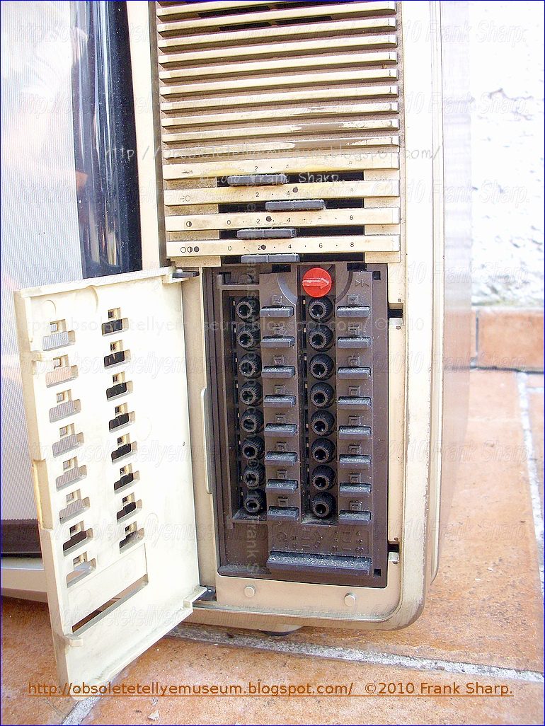
 The ITT IDEAL COLOR 3214 OSCAR is a 15 inches portable color television with 16 programs KEYBOARD selection and potentiometric tuning search.

  • The mechanical turret approach to television tuning has been used almost exclusively for the past 60 years. Even though replete with the inherent disadvantages of mechanical complexity, unreliability and cost, such apparatus has been technically capable of performing its intended function and as a result the consumer has had to bear the burdens associated with the device. However, with the " recent " Broadcast demands for parity of tuning for UHF and VHF channels, the increasing number of UHF and cable TV stations have imposed new tuning performance requirements which severely tax the capability of the mechanical turret tuner. Consequently, attempts are now being made to provide all electronic tuning to meet the new requirements.

The invention relates to a tuning unit with bandswitch for high frequency receivers, especially radio and television receivers, having a potentiometer system for the control of capacity diodes, the said potentiometer system consisting of a plurality of parallel resistance paths along which wiper contacts can be driven by means of screw spindles disposed adjacent one another in a common insulating material housing in which a bandswitch formed of metal rods is associated with each tuning spindle.
In these tuning units, the working voltages of the capacity diodes in the tuning circuits are recorded once a precise tuning to the desired frequency has been performed. A potentiometer tuning system has great advantages over the formerly used channel selectors operating with mechanically adjustable capacitors (tuning condensers) or mechanically adjustable inductances (variometers), mainly because it is not required to have such great precision in its tuning mechanism.
Tuning units with bandswitches formed of variable resistances and combined with interlocking pushbuttons controlling the supply of recorded working voltages to capacity diodes are known. Channel selection is accomplished by depressing the knobs, and the tuning or fine tuning are performed by turning the knobs. The resistances serving as voltage dividers in these tuning units are combined into a component unit such that they are in the form of a ladderlike pattern on a common insulating plate forming the cover of the housing in which the tuning spindles and wiper contacts corresponding to the variable resistances are housed. The number of resistances corresponds to the number of channels or frequencies which are to be recorded. The wiper contact picks up a voltage which, when applied to the capacity diodes determines their capacitance and hence the frequency of the corresponding oscillating circuit. The adjustment of the wipers is performed by turning the tuning spindle coupled to the tuning knob. By the depression of a button the electrical connection between a contact rod and a tuning spindle is brought about and thus the selected voltage is applied to the capacity diodes. Since the push buttons release one another, it is possible simply by depressing another button to tune to a different receiving frequency or a different channel, as the case may be.
 Moreover, using this arrangement, the only indication--during adjustment--of which channel is selected is by station identification.
In the end of the 60's 70's increasingly attention was focused on the varicap diode tuner as the latest, sophisticated means of television receiver frontend tuning in both colour and black and white sets. 

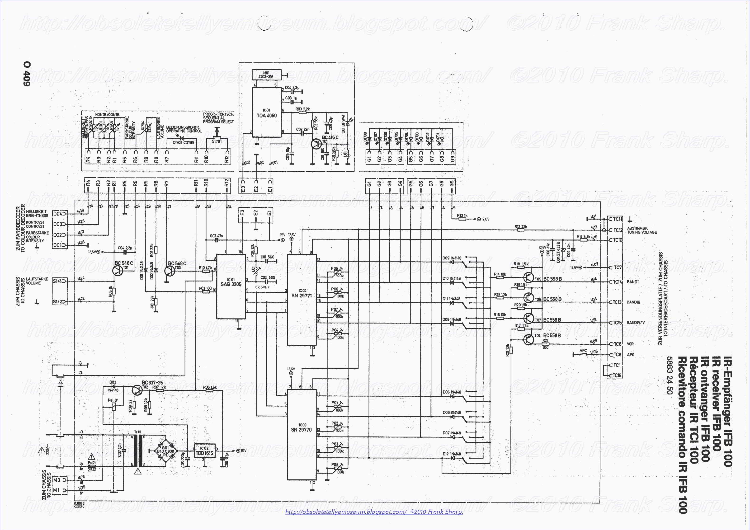
The tuning has a manual AFC red button to deactivate it during search.

The general concept of Automatic Frequency Control (AFC) for television receivers is known in the art and has been adapted to radio receivers as well as to television receivers of both the monochrome and color variety. The general purpose of such a system is to assist the user in attaining proper fine-tuning of the receiver without requiring critical manual adjustment. The advantage of such a system is self-evident but its value to a color receiver is markedly increased due to the fact that improper tuning of a color receiver manifests itself in incorrect colors, or even a total lack of color, in the reproduced image.

Typically, the AFC system is tuned to a reference or center frequency corresponding to the desired video IF frequency and so long as the tuning is reasonably close, within the response of the AFC system, an error voltage is developed to correct the tuning. If the user of the television receiver makes the fine-tuning adjustment while the AFC system is operative, he may adjust it to a point where the picture is acceptable but a substantial amount of AFC correction voltage is required. Thus, the receiver may be tuned at the limit of the "hold-in" range and would not give the proper "pull-in" performance when the channel selector is switched to the next channel. Accordingly, it is desirable to include an AFC defeat circuit for disabling the AFC system during manual fine-tuning. Heretofore, most AFC defeat circuits have required that the user of the television receiver defeat the AFC system by means of a manual switch. It is apparent, however, that the typical user of a television receiver may at times forget to flip the switch and hence the attendant problems are realized.

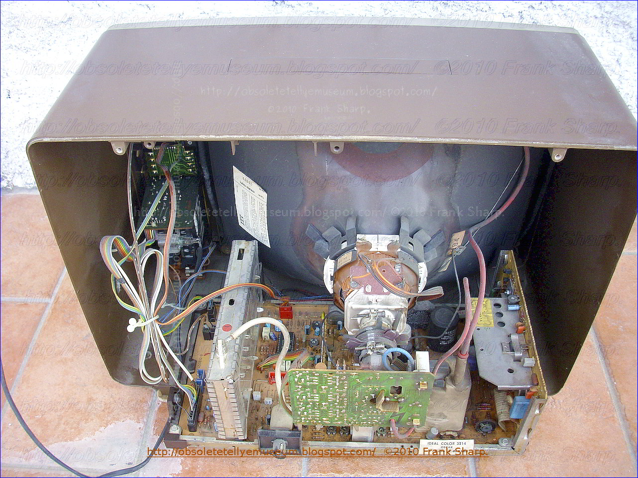
  • The set features a black matrix color picture tube.This invention relates to a black matrix color picture tube and a method for its fabrication and particularly to a high-contrast black matrix color picture tube and a method for its fabrication.

The phosphor screen of a so-called black matrix color picture tube has on its faceplate the formation of a nonluminous, light-absorptive powder layer (black matrix) for partly covering the phosphor layer so that the phosphor layer appears through aperture sections (matrix holes).  A method of reducing the inner surface reflection has been proposed, in which a material having virtually the same refractivity as the faceplate material, e.g., water glass, is filled in the gap between the faceplate and the black matrix layer. See, for example, JP-A-57-115749.

A black matrix color picture tube has a phosphor layer and black matrix layer formed on the inner surface of the faceplate. A layer of glass having a low softening point is provided between the phosphor layer and the inner surface of the faceplate and between the black matrix layer and the inner surface of the faceplate. The softening point of the glass is below the temperature at which the tube is subjected during a frit baking step employed in the fabrication of the tube. For example, a borophosphate glass is used as the layer of glass having a low softening point.


  •  Above the program selection keyboard manual controls for volume,brightness,contrast,color saturation with slide potentiometers.
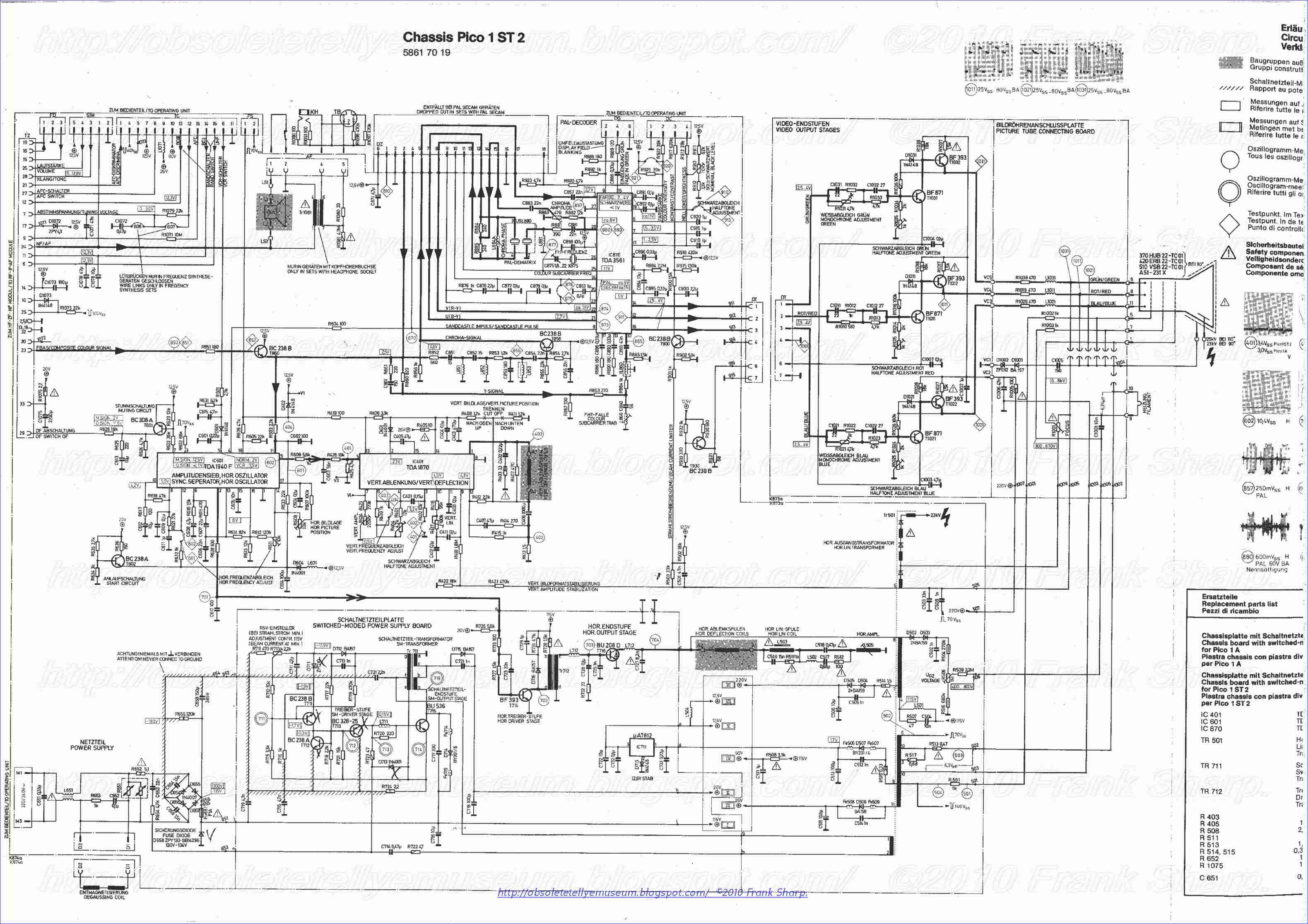
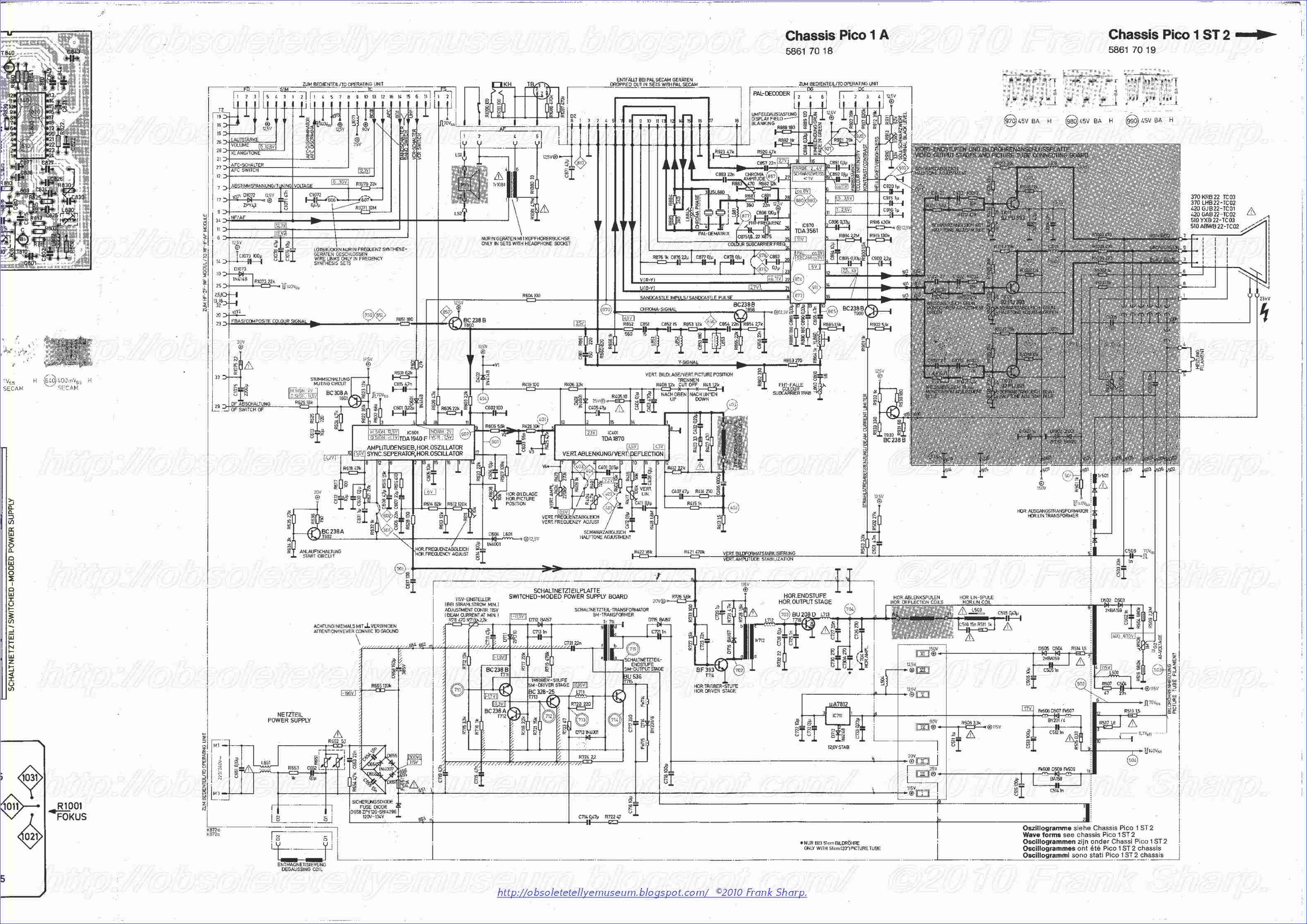
  •  The set  was featuring the PICO 1A chassis allowing  the fitting of a integrated TV Color chassis in little dimensions comprising all functions of the receiver having the legacy with very bigger types fitted in earlier models.
  •  Was first ITT Portable color television featuring the PHILIPS TDA3560A a decoder for the PAL colour television standard. It combines all functions required for the identification and demodulation of PAL signals.
    Furthermore it contains a luminance amplifier, an RGB-matrix and amplifier.
  • Above a hand grip is present and a pair of expandable telescopic antennas.

NO SCART connector is present.

Pictures are EXCELLENT !!.................Sound too.

----------------------------------------------------------------------------


ITT Corporation (NYSE: ITT) is a global diversified manufacturing company with 2008 revenues of $11.7 billion. ITT participates in global markets including water and fluids management, defense and security, and motion and flow control. Forbes.com named ITT Corporation to its list of "America's Best Managed Companies" for 2008, and awarded the company the top spot in the conglomerates category.

,ITT's water business is the world's largest supplier of pumps and systems to transport, treat and control water, and other fluids. The company's defense electronics and services business is one of the ten largest US defense contractors providing defense and security systems, advanced technologies and operational services for military and civilian customers. ITT's motion and flow control business manufactures specialty components for aerospace, transportation and industrial markets.

In 2008, ITT was named to the Dow Jones Sustainability World Index (DJSI World) for the tenth time in recognition of the company's economic, environmental and social performance. ITT is one of the few companies to be included on the list every year since its inception in 1999.

The company was founded in 1920 as International Telephone & Telegraph. During the 1960s and 1970s, under the leadership of its CEO Harold Geneen the company rose to prominence as the archetypal conglomerate, deriving its growth from hundreds of acquisitions in diversified industries. ITT divested its telecommunications assets in 1986, and in 1995 spun off its non-manufacturing divisions, later to be purchased by Starwood Hotels & Resorts Worldwide.

In 1996, the company became ITT Industries, Inc., but changed its name back to ITT Corporation in 2006.


History

ITT was formed in 1920, created from the Puerto Rico Telephone Company co-founded by Sosthenes Behn.
 Its first major expansion was in 1923 when it consolidated the Spanish Telecoms market into what is now Telefónica.[
From 1922 to 1925 it purchased a number of European telephone companies. In 1925 it purchased the Bell Telephone Manufacturing Company of Brussels, Belgium, which was formerly affiliated with AT&T, and manufactured rotary system switching equipment. In the 1930s, ITT grew through purchasing German electronic companies Standard Elektrizitaetsgesellschaft (SEG) and Mix & Genest, both of which were internationally active companies. Its only serious rival was the Theodore Gary & Company conglomerate, which operated a subsidiary, Associated Telephone and Telegraph, with manufacturing plants in Europe.

In the United States, ITT acquired the various companies of the Mackay Companies in 1928 through a specially organized subsidiary corporation, Postal Telegraph & Cable. These companies included the Commercial Cable Company, the Commercial Pacific Cable Company, Postal Telegraph, and the Federal Telegraph Company.


International telecommunications

International telecommunications manufacturing subsidiaries included STC in Australia and Britain, SEL in Germany, BTM in Belgium, and CGCT and LMT in France. Alec Reeves invented Pulse-code modulation (PCM), upon which future digital voice communication was based. These companies manufactured equipment according to ITT designs including the (1960s) Pentaconta crossbar switch and (1970s) Metaconta D, L and 10c Stored Program Control exchanges, mostly for sale to their respective national telephone administrations. This equipment was also produced under license in Poznań (Poland), and in Yugoslavia, and elsewhere. ITT was the largest owner of the LM Ericsson company in Sweden but sold out in 1960.


1989 breakup

In 1989 ITT sold its international telecommunications product businesses to Alcatel, now Alcatel-Lucent. ITT Kellogg was also part of the 1989 sale to Alcatel. The company was then sold to private investors in the U.S. and went by the name Cortelco Kellogg. Today the company is known as Cortelco (Corinth Telecommunications Corporation, named for Corinth, MS headquarters). ITT Educational Services, Inc. (ESI) was spun off through an IPO in 1994, with ITT as an 83% shareholder. ITT merged its long distance division with Metromedia Long Distance, creating Metromedia-ITT. Metromedia-ITT would eventually be acquired by Long Distance Discount Services, Inc. (LDDS) in 1993. LDDS would later change its name to Worldcom in 1995.

In 1995, ITT Corporation split into 3 separate public companies:

* ITT Corp. — In 1997, ITT Corp. completed a merger with Starwood Hotels & Resorts Worldwide, selling off its non-hotel and resorts business. By 1999, ITT completely divested from ITT/ESI; however, the schools still operate as ITT Technical Institute using the ITT name under license.[1] Also in 1999, ITT Corp. dropped the ITT name in favor of Starwood.
* ITT Hartford (insurance) — Today ITT Hartford is still a major insurance company although it has dropped the ITT from its name altogether. The company is now known as The Hartford Financial Services Group, Inc.
* ITT Industries — ITT operated under this name until 2006 and is a major manufacturing and defense contractor business.
o On July 1, 2006, ITT Industries changed its name to ITT Corporation as a result of its shareholders vote on May 9, 2006.


Purchase of International Motion Control (IMC)

An agreement was reached on June 26, 2007 for ITT to acquire privately held International Motion Control (IMC) for $395 million. The deal was closed and finalized in September 2007. An announcement was made September 14, 2010, to close the Cleveland site.
Purchase of EDO

An agreement was reached September 18, 2007 for ITT to buy EDO Corporation for $1.7 billion. After EDO shareholders' approval, the deal was closed and finalized on December 20, 2007.


Purchase of Laing

On April 16, 2009, ITT announced it has signed a definitive agreement to acquire Laing GmbH of Germany, a privately held leading producer of energy-efficient circulator pumps primarily used in residential and commercial plumbing and heating, ventilating and air conditioning (HVAC) systems.


2011 breakup

On January 12, 2011, ITT announced a transformation to separate the company into 3, stand-alone, publicly-traded, and independent companies.


HISTORY OF Standard Elektrik Lorenz AG IN GERMAN:

Die Standard Elektrik Lorenz AG (heute Alcatel-Lucent Deutschland AG) ist ein Unternehmen der Nachrichtentechnik (früherer Slogan: SEL – Die ganze Nachrichtentechnik) mit Hauptsitz in Stuttgart. Zur Nachrichtentechnik zählen auch Informations- und Kommunikationstechnik, Telekommunikationstechnik (SEL war für die Röchelschaltung bekannt) und früher Fernmeldetechnik oder Schwachstromtechnik. Einen weiteren Geschäftsbereich hatte das Unternehmen in der Bahnsicherungstechnik, so wurden für die Deutsche Bundesbahn Relaisstellwerke und elektronische Stellwerke mit den dazugehörigen Außenanlagen (Signale, Gleisfreimeldeanlagen, Weichenantriebe) sowie die Linienzugbeeinflussung entwickelt und gebaut, welche auch bei ausländischen Bahnen Abnehmer fanden. Der Bereich gehört seit 2007 als Thales Transportation Systems GmbH (seit 02.2011 vorher Thales Rail Signalling Solutions GmbH) zum Thales-Konzern. Die bereits 1998 ausgegliederten Bereiche Alcatel Air Navigation Systems und SEL Verteidigungssysteme sind ebenfalls heute in Thales Deutschland beheimatet.
Fernseher Illustraphon 743 von 1957
„Goldsuper Stereo 20“ (1961)
Das Flaggschiff der erfolgreichen Schaub-Lorenz Kofferradios der sechziger Jahre: Touring 70 Universal
Erster Digitalfernseher der Welt (1983)

Bis 1987 gehörte SEL zusammen mit anderen auf dem Sektor Telekommunikation in anderen Ländern tätigen Schwesterfirmen zum US-amerikanischen Mischkonzern International Telephone and Telegraph (ITT). ITT verkaufte die Aktien-Mehrheit an den ITT-Telekommunikationsfirmen an die französische Compagnie Générale d’Electricité (CGE), die nach der Zusammenfassung mit den eigenen Telekommunikationsaktivitäten daraus die Alcatel N.V. bildete.

Die Standard Elektrik Lorenz AG wurde 1993 in Alcatel SEL AG umbenannt. Die Aktienmehrheit liegt mit über 99 % bei der Alcatel. Mit der Fusion von Alcatel und Lucent zu Alcatel-Lucent am 1. Dezember 2006 und der Neu-Firmierung beider Unternehmen in Deutschland zur Alcatel-Lucent Deutschland AG entfiel der Zusatz SEL.


Geschichte

Die beiden Stammfirmen des Unternehmens, die Mix & Genest AG und die Telegraphenbauanstalt von C. Lorenz, wurden 1879 bzw. 1880 gegründet. Das erste Patent von Mix & Genest datiert von 1883, das erste Patent von C. Lorenz ist aus dem Jahr 1902.

Das Unternehmen Mix & Genest war wesentlicher Teil der Standard Elektrizitäts-Gesellschaft (SEG), in die auch die Süddeutsche Apparatefabrik (SAF), die 1875 von F. Heller als "Friedrich Heller, Fabrik Elektrotechnischer Apparate" gegründet wurde, integriert wurde. Der technische Schwerpunkt von Mix & Genest bzw. SEG sowie der C. Lorenz AG war der klassischen Fernmelde- bzw. Funktechnik zuzuordnen. Die C. Lorenz AG baute in den 1920er und 1930er Jahren Großsender für den neu gegründeten Rundfunk.

1930 übernahm die International Telephone and Telegraph Company (ITT) die Aktienmehrheit der Mix & Genest AG und der C. Lorenz AG.

Die C. Lorenz AG positionierte sich mit der Übernahme der G. Schaub Apparatebau-Gesellschaft mbH im Jahr 1940 in der Entwicklung und Herstellung von Rundfunkempfängern. Ab dem Jahr 1950 wurden alle Geräte bei Schaub in Pforzheim gefertigt. 1952 wurde das Typenprogramm beider Unternehmen verschmolzen und der Lorenz-Radio-Vertrieb in die Firma Schaub integriert. Ab 1955 wurden die Geräte unter dem Namen Schaub-Lorenz vertrieben.

1956 wurde das Unternehmen SEG in Standard Elektrik AG umbenannt. Ebenfalls 1956 wurde ein Kabelwerk gegründet. Wesentlicher Motor für das 1957 gegründete Informatikwerk war Karl Steinbuch, der von 1948–1958 dem Unternehmen, zuletzt als Technischer Direktor und Leiter der Zentralen Forschung, angehörte.

1958 erfolgte die Vereinigung der Standard Elektrik AG mit der C. Lorenz AG zur Standard Elektrik Lorenz AG (SEL).

Die Standard Elektrik Lorenz AG übernahm 1961 die Graetz KG. Die Firmenteile Schaub-Lorenz und Graetz waren zusammen mit einem Bildröhrenwerk Bestandteil der Unternehmensgruppe Audio Video der SEL AG, die 1979 als Audio-Video-Elektronik in die ITT ausgegliedert wurde. Die Produkte, die unter anderem Fernsehgeräte, Radios, Autoradios, Kassettenrecorder, Weltempfänger und Lautsprecherboxen umfassen, wurden fortan unter dem Namen ITT Schaub-Lorenz vertrieben.

Versuche, auf dem neuen Gebiet der Raumfahrt-Elektronik Fuß zu fassen, waren auf folgende Produkte beschränkt:

* AZUR: Telemetrie/Telekommandogeräte
* Spacelab: Datenerfassung/Kommandoterminal.

SEL entwickelte zu Beginn der 1970er Jahre das Präzisionsanflugverfahren SETAC. Dieser Unternehmensbereich wurde im Jahre 1987 von der finnischen Firma Nokia übernommen.

1976 hatte SEL ein Grundkapital von 357 Mio. DM bei 33.000 Beschäftigten und einem Umsatz von 2,6 Mrd. DM.


1983 stellte S E L auf der Internationalen Funkausstellung Berlin 1983 mit dem ITT Digivision den weltweit ersten Fernseher mit digitaler Signalverarbeitung vor.

2003 wurden die Markenrechte am Namen Schaub Lorenz an die italienische General Trading SpA verkauft. Die neugegründete Schaub Lorenz International GmbH vertreibt seitdem unter dem alten Markennamen Schaub-Lorenz importierte Konsumelektronik aus dem unteren Preisbereich.


References:
 

Demerjian, Dave (25 October 2007). "As Skies Grow Crowded, FAA Preps Air Traffic Control 2.0". Wired.com. Archived from the original on 14 June 2013. Retrieved 25 May 2013.
"ITT Corporation 2017 Annual Report Form (10-K)" (XBRL). United States Securities and Exchange Commission. February 14, 2018.
"ITT Corporation 2016 Annual Report Form (8-K)" (XBRL). United States Securities and Exchange Commission. February 14, 2017. Archived from the original on March 16, 2017.
"ITT History". ITT Inc. Archived from the original on 2017-08-03. Retrieved 2017-08-02.
"At A Glance | ITT Inc". www.itt.com. Retrieved 2019-01-09.
www.itt.com https://www.itt.com/CMSPages/GetFile.aspx?guid=10cffa55-7c3c-4e27-b649-d0378feddc07. Retrieved 2019-01-09. Missing or empty |title= (help)
"ITT to break itself up, fueling share rally". Reuters. January 12, 2011. Archived from the original on July 1, 2012. Retrieved July 14, 2011.
Jacobs, Karen (July 14, 2011). "UPDATE 1-ITT sets names for planned spin-offs". Reuters. Archived from the original on July 1, 2012. Retrieved July 14, 2011.
Sobel, Robert (2000). ITT: The Management of Opportunity. Beard Books. pp. 35ff.
Macintosh, Norman B.; Paolo Quattrone (2009). Management Accounting and Control Systems. John Wiley and Sons. pp. 155–6.
Ingham, John N. (1983). Biographical dictionary of American business leaders, Volume 1. Greenwood Publishing Group. pp. 62–4.
Sampson, Anthony. The Sovereign State of ITT, Hodder and Stoughton, 1973. ISBN 0-340-17195-2
Garcia Algarra, Javier (2010). "The American influence in Telefónica's public relations strategy during the 20s and 30s" Archived 2013-06-01 at the Wayback Machine, IEEE HISTELCON 2010
AMERICAN VISITS HITLER. Behn of National City Bank Confers With Chancellor in Alps. New York Times, 1933-08-04, "Archived copy". Archived from the original on 2014-03-07. Retrieved 2013-05-16.
»Empfänge beim Reichskanzler«, Vossische Zeitung, Berlin 1933-08-04, Abendausgabe, Seite 3, "Archived copy". Archived from the original on 2014-03-07. Retrieved 2013-05-03.
The Office of Military Government US Zone in Post-war Germany 1946-1949, declassified per Executive Order 12958, Section 3.5 NND Project Number: NND 775057 by: NND Date: 1977
Leidig, Ludwig. Bombshell. sbpra, 2013 ISBN 978-1-62516-346-2
Farnsworth, Emma. "Farnsworth, Philo T. and Elma G." J. Willard Marriott Library, University of Utah. Archived from the original on 14 July 2014. Retrieved 8 July 2014.
"KONI shock absorbers". Archived from the original on 2015-05-18.
International Telephone and Telegraph Corporation Archived 2012-01-22 at the Wayback Machine at Funding Universe
Knippers Black, Jan (1977). United States Penetration of Brazil. The University of Pennsylvania Press. pp. 40–49.
Langguth, A. J. (1979). Hidden Terrors: The Truth about U.S. Police Operations in Latin America. New York: Pantheon Books.
Green, James (2010). We Cannot Remain Silent: Opposition to the Brazilian Military Dictatorship in the United States. Durham and London: Duke University Press. p. 89. ISBN 978-0-8223-4735-4.
Burn Before Reading, Admiral Stansfield Turner, 2005, Hyperion, pg. 99. Also see the article on Humberto de Alencar Castelo Branco. Also see BRAZIL MARKS 40th ANNIVERSARY OF MILITARY COUP Archived 2008-11-20 at the Wayback Machine, National Security Archive, George Washington University. Edited by Peter Kornbluh, 2004.
Ancona, Vincent S. (Fall 1992). "When the Elephants Marched out of San Diego". Journal of San Diego History. San Diego Historical Society. 38 (4). Archived from the original on 2013-07-05.
"ITT: No charges". Time Magazine. June 10, 1974. Archived from the original on 19 October 2012. Retrieved 24 October 2012. United States and American History: 1972 Archived 2007-03-18 at the Wayback Machine at trivia-library.com
Hinchey Report Archived 2009-10-20 at the Wayback Machine at US Dept. of State
Stout, David (January 30, 2003). "Edward Korry, 81, Is Dead; Falsely Tied to Chile Coup". The New York Times. Archived from the original on May 12, 2013. Retrieved May 5, 2010.
The Pinochet File: How U.S. Politicians, Banks and Corporations Aided Chilean Coup, Dictatorship Archived 2015-09-12 at the Wayback Machine. Democracy Now! September 10, 2013.
Montgomery, Paul L. (September 29, 1973). "I.T.T. OFFICE HERE DAMAGED BY BOMB; Caller Linked Explosion at Latin-American Section to 'Crimes in Chile' I.T.T. Latin-American Office on Madison Ave. Damaged by Bomb Fire in Rome Office Bombing on the Coast Rally the Opponents". The New York Times. Archived from the original on May 12, 2011. Retrieved May 5, 2010.
Ayers, Bill. Sing a Battle Song: The Revolutionary Poetry, Statements, and Communiques of The Weather Underground
Wasserstein, Bruce. Big deal: the battle for control of America's leading corporations
Associated Press (23 November 1997). "Obituary: Harold Geneen, 87; Led ITT's Growth for 18 Years". The New York Times. Archived from the original on 27 March 2016.
Viswanathan, T. Telecommunication Switching Systems and Networks, p.225.
US Patent 4,201,891 at freepatentsonline.com
International Telephone Telegraph Corp at encyclopedia.com
Magnet, Myron; Andrew Evan Serwer (11 November 1985). "IS ITT FIGHTING SHADOWS -- OR RAIDERS?". Fortune. Archived from the original on 29 April 2014.
Chapuis, Robert J.; Joel, Amos E., Jr. "IX-7: "The ITT (now Alcatel) System 12"". 100 Years of Telephone Switching.
"ITT Earnings Decline 33% for 3rd Quarter" Archived 2011-12-24 at Wikiwix, Los Angeles Times, 5 November 1985.
Bartlett, Christopher A.; Ghoshal, Sumantra (2002). Managing Across Borders (2 ed.). Harvard Business School Press. ISBN 978-1-57851-707-7.
ITT Telecom Archived 2016-12-20 at the Wayback Machine, The New York Times, 26 June 1984.
"ITT Makes Sale To Southern Bell" Archived 2016-12-20 at the Wayback Machine, The New York Times, 21 March 1985.
ITT System 12 Archived 2016-09-20 at the Wayback Machine at frankoverstreet.com
Hinman, Catherine."ITT Division In Brevard Will Furlough 60" Archived 2011-12-23 at Wikiwix, Orlando Sentinel, 14 March 1986.
Alcatel-Lucent Timeline Archived 2012-02-03 at the Wayback Machine at alcatel-lucent.com
Alcatel SA Company History Archived 2012-01-22 at the Wayback Machine at Funding Universe
"ITT Accepts $3.6 Billion Alcatel Sale" Archived 2016-03-06 at the Wayback Machine, The New York Times, 4 March 1992.
"Archived copy". Archived from the original on 2016-09-08. Retrieved 2016-09-13. ITT Tech closes its doors, blaming ‘unconstitutional’ US sanctions
"COMPANY NEWS; Metromedia Deal For 2 ITT Units" Archived 2017-12-19 at the Wayback Machine, The New York Times, 16 March 1989.
"Company News; Starwood Lodging in $2.1 Billion Deal with Vnu". The New York Times. 1997-12-19. ISSN 0362-4331. Retrieved 2018-05-29.
Webpage at ITTESI.com Archived October 22, 2006, at the Wayback Machine
Nunez, Michael (September 6, 2016). "ITT Tech Is Officially Closing". Gizmodo. Archived from the original on September 6, 2016. Retrieved September 6, 2016.
Center, Arbitration and Mediation. "WIPO Domain Name Decision: D2001-0166". Archived from the original on 2001-06-10.
Lindsey, Sue. "ITT Fined $100M for Illegal Tech Exports"[dead link], Associated Press, March 27, 2007.
Cullen, Drew. "ITT Fined for Illegal Exports" Archived 2011-02-24 at Wikiwix, The Register, 27 March 2007.
"Consent Agreement, 2007: ITT Corporation" Archived 2009-10-10 at the Wayback Machine U.S. State Department, 2007.
"ITT fined $100 million for illegal exports". CNN. 27 March 2007. Archived from the original on 28 March 2010. Retrieved May 5, 2010.
"ITT Corp. Acquires EDO in $1.7B Deal". Archived from the original on 2016-08-17.
"Archived copy". Archived from the original on 2011-09-23. Retrieved 2009-01-03. 67 (block): The International Telephone and Telegraph Building, erected in 1928 by Garment District developer Abraham Lefcourt as the Lefcourt Exchange Building, was almost immediately bought by ITT--which expanded the building to take over the whole block by 1930.
Holusha, John. "Commercial Property /75 Broad Street; Turning Buildings Into Telecommunications Hubs" Archived 2016-03-16 at the Wayback Machine, The New York Times, 10 October 1999.
http://www.thecityreview.com/parkave.html. Archived from the original on 2012-01-20. Missing or empty |title= (help)
Deutsch, Claudia H. (21 May 1989). "REFORGING THE 'GENEEN MACHINE'". The New York Times. Archived from the original on 28 August 2016.
"International Telephone & Telegraph ITT Information and History". Archived from the original on 2016-03-29.
"Radio Tower Demolished". The New York Times. 5 April 1996. Archived from the original on 22 July 2010. Retrieved 2010-07-23.
"ITT Avionics Gets $19.6M Air Force Pact". Bergen Record. 19 September 1991. Archived from the original on 18 May 2013. Retrieved 2010-07-23.
(August 20, 2004.) "ITT Industries Receives Contract for $24.9 Million." Archived 2012-04-20 at the Wayback Machine Impeller.net Archived 2011-11-01 at the Wayback Machine. Accessed November 2011.
(in German) http://1.bp.blogspot.com/-_lUfX51dGQA/T5rl4WcLLdI/AAAAAAAALyY/0qWIKzVoA04/s1600/ITT-2805_SLK-AD2.jpg. Archived from the original on 2018-05-01. Missing or empty |title= (help)
"Consola "pong" Tele-Match (versión con paddle) (1977)". retroordenadoresorty.blogspot.it (in Spanish). Archived from the original on 1 May 2018. Retrieved 14 February 2018.
"ITT DIGIVISION 3447 OSCAR YEAR 1986". Obsolete Technology Tellye. Retrieved 14 February 2018.
"Kellogg Switchboard & Supply Co". Dictionary of Leading Chicago Businesses. Archived from the original on 18 August 2015. Retrieved 15 February 2018.
"Über ITT - ITT". www.itt-deutschland.de (in German). Archived from the original on 17 October 2017. Retrieved 15 February 2018.
"Nokia Announces Final Sale of its Television Manufacturing Business - Nokia". Nokia. Archived from the original on 2017-07-29.
"Über Karcher - ITT". www.itt-deutschland.de (in German). Archived from the original on 22 December 2016. Retrieved 14 February 2018.

--------------------------------------------------------------------------------------------------------------------------------------------------------------


R.I.P.  EUROPE !


ITT IDEAL COLOR 3214 OSCAR CHASSIS PICO 1A INTERNAL VIEW


ITT IDEAL COLOR 3214 OSCAR  CHASSIS PICO 1A CIRCUIT ARRANGEMENT IN A PICTURE DISPLAY DEVICE UTILIZING A STABILIZED SUPPLY VOLTAGE CIRCUIT:
A stabilized supply voltage circuit for a picture display device comprising a chopper wherein the switching signal has the line frequency and is duration-modulated. The coil of the chopper constitutes the primary winding of a transformer a secondary winding of which drives the line output transistor so that the switching transistor of the chopper also functions as a driver for the line output stage. The oscillator generating the switching signal may be the line oscillator. In a special embodiment the driver and line output transistor conduct simultaneously and in order to limit the base current of the line output transistor a coil shunted by a diode is incorporated in the drive line of the line output transistor. Other secondary windings of the transformer drive diodes which conduct simultaneously with the efficiency diode of the chopper so as to generate further stabilized supply voltages.


1. An electrical circuit arrangement for a picture display device operating at a given line scanning frequency, comprising a source of unidirectional voltage, an inductor, first switching transistor means for periodically energizing said inductor at said scanning frequency with current from said source, an electrical load circuit coupled to said inductor and having applied thereto a voltage as determined by the ratio of the ON and OFF periods of said transistor, means for maintaining the voltage across said load circuit at a given value comprising means for comparing the voltage of said load circuit with a reference voltage, means responsive to departures of the value of the load circuit voltage from the value of said reference voltage for varying the conduction ratio of the ON and OFF periods of said transistor thereby to stabilize said load circuit voltage at the given value, a line deflection coil system for said picture display device, means for energizing said line deflection coil system from said load voltage circuit means, means for periodically interrupting the energization of said line deflection coil comprising second switching means and means coupled to said inductor for deriving therefrom a switching current in synchronism with the energization periods of said transistor and applying said switching current to said switching means thereby to actuate the same, and means coupled to said switching means and to said load voltage circuit for producing a voltage for energizing said 2. A circuit as claimed in claim 1 wherein the duty cycle of said switching 3. A circuit as claimed in claim 1 further comprising an efficiency first 4. A circuit as claimed in claim 3 further comprising at least a second diode coupled to said deriving means and to ground, and being poled to 5. A circuit as claimed in claim 1 wherein said second switching means comprises a second transistor coupled to said deriving means to conduct simultaneously with said first transistor, and further comprising a coil coupled between said driving means and said second transistor and a third diode shunt coupled to said coil and being poled to conduct when said 6. A circuit as claimed in claim 1 further comprising a horizontal oscillator coupled to said first transistor, said oscillator being the 7. A circuit as claimed in claim 1 further comprising means coupled to said inductor for deriving filament voltage for said display device.

Description:
The invention relates to a circuit arrangement in a picture display device wherein the input direct voltage between two input terminals, which is obtained be rectifying the mains alternating voltage, is converted into a stabilized output direct voltage by means of a switching transistor and a coil and wherein the transistor is connected to a first input terminal and an efficiency diode is connected to the junction of the transistor and the coil. The switching transistor is driven by a pulsatory voltage of line frequency which pulses are duration-modulated in order to saturate the switching transistor during part of the period dependent on the direct voltage to be stabilized and to cut off this transistor during the remaining part of the period. The pulse duration modulation is effected by means of a comparison circuit which compares the direct voltage to be stabilized with a substantially constant voltage, the coil constituting the primary winding of a transformer.

Such a circuit arrangement is known from German "Auslegeschrift" 1.293.304. wherein a circuit arrangement is described which has for its object to convert an input direct voltage which is generated between two terminals into a different direct voltage. The circuit employs a switch connected to the first terminal of the input voltage and periodically opens and closes so that the input voltage is converted into a pulsatory voltage. This pulsatory voltage is then applied to a coil. A diode is arranged between the junction of the switch and the coil and the second terminal of the input voltage whilst a load and a charge capacitor in parallel thereto are arranged between the other end of the coil and the second terminal of the input voltage. The assembly operates in accordance with the known efficiency principle i.e., the current supplied to the load flows alternately through the switch and through the diode. The function of the switch is performed by a switching transistor which is driven by a periodical pulsatory voltage which saturates this transistor for a given part of the period. Such a configuration is known under different names in the literature; it will be referred to herein as a "chopper." A known advantage thereof, is that the switching transistor must be able to stand a high voltage or provide a great current but it need not dissipate a great power. The output voltage of the chopper is compared with a constant reference voltage. If the output voltage attempts to vary because the input voltage and/or the load varies, a voltage causing a duration modulation of the pulses is produced at the output of the comparison arrangement. As a result the quantity of the energy stored in the coil varies and the output voltage is maintained constant. In the German "Auslegeschrift" referred to it is therefore an object to provide a stabilized supply voltage device.

In the circuit arrangement according to the mentioned German "Auslegeschrift" the frequency of the load variations or a harmonic thereof is chosen as the frequency for the switching voltage. Particularly when the load fed by the chopper is the line deflection circuit of a picture display device, wherein thus the impedance of the load varies in the rhythm of the line frequency, the frequency of the switching voltage is equal to or is a multiple of the line frequency.

It is to be noted that the chopper need not necessarily be formed as that in the mentioned German "Auslegeschrift." In fact, it is known from literature that the efficiency diode and the coil may be exchanged. It is alternatively possible for the coil to be provided at the first terminal of the input voltage whilst the switching transistor is arranged between the other end and the second terminal of the input voltage. The efficiency diode is then provided between the junction of said end and the switching transistor and the load. It may be recognized that for all these modifications a voltage is present across the connections of the coil which voltage has the same frequency and the same shape as the pulsatory switching voltage. The control voltage of a line deflection circuit is a pulsatory voltage which causes the line output transistor to be saturates and cut off alternately. The invention is based on the recognition that the voltage present across the connections of the coil is suitable to function as such a control voltage and that the coil constitutes the primary of a transformer. To this end the circuit arrangement according to the invention is characterized in that a secondary winding of the transformer drives the switching element which applies a line deflection current to line deflection coils and by which the voltage for the final anode of a picture display tube which forms part of the picture display device is generated, and that the ratio between the period during which the switching transistor is saturated and the entire period, i.e., the switching transistor duty cycle is between 0.3 and 0.7 during normal operation.

The invention is also based on the recognition that the duration modulation which is necessary to stabilize the supply voltage with the switching transistor does not exert influence on the driving of the line output transistor. This resides in the fact that in case of a longer or shorter cut-off period of the line output transistor the current flowing through the line deflection coils thereof is not influenced because of the efficiency diode current and transistor current are taken over or, in case of a special kind of transistor, the collector-emitter current is taken over by the base collector current and conversely. However, in that case the above-mentioned ratios of 0.3 : 0.7 should be taken into account since otherwise this take-over principle is jeopardized.

As will be further explained the use of the switching transistor as a driver for the line output transistor in an embodiment to be especially described hereinafter has the further advantage that the line output transistor automatically becomes non-conductive when this switching transistor is short circuited so that the deflection and the EHT for the display tube drop out and thus avoid damage thereof.

Due to the step according to the invention the switching transistor in the stabilized supply functions as a driver for the line deflection circuit. The circuit arrangement according to the invention may in addition be equipped with a very efficient safety circuit so that the reliability is considerably enhanced, which is described in the U.S. Pat. No. 3,629,686. The invention is furthermore based on the recognition of the fact that the pulsatory voltage present across the connections of the coil is furthermore used and to this end the circuit arrangement according to the invention is characterized in that secondary windings of the transformer drive diodes which conduct simultaneously with the efficiency diode so as to generate further stabilized direct voltages, one end of said diodes being connected to ground.

In order that the invention may be readily carried into effect, a few embodiments thereof will now be described in detail by way of example with reference to the accompanying diagrammatic drawings in which:

FIG. 1 shows a principle circuit diagram wherein the chopper and the line deflection circuit are further shown but other circuits are not further shown.

FIGS. 2a, 2b and 2c show the variation as a function of time of two currents and of a voltage occurring in the circuit arrangement according to FIG. 1.

FIGS. 3a 3b, 3c and 3d show other embodiments of the chopper.

FIGS. 4a and 4b show modifications of part of the circuit arrangement of FIG. 1.

In FIG. 1 the reference numeral 1 denotes a rectifier circuit which converts the mains voltage supplied thereto into a non-stabilized direct voltage. The collector of a switching transistor 2 is connected to one of the two terminals between which this direct voltage is obtained, said transistor being of the npn-type in this embodiment and the base of which receives a pulsatory voltage which originates through a control stage 4 from a modulator 5 and causes transistor 2 to be saturated and cut off alternately. The voltage waveform 3 is produced at the emitter of transistor 2. In order to maintain the output voltage of the circuit arrangement constant, the duration of the pulses provided is varied in modulator 5. A pulse oscillator 6 supplies the pulsatory voltage to modulator 5 and is synchronized by a signal of line frequency which originates from the line oscillator 6' present in the picture display device. This line oscillator 6' is in turn directly synchronized in known manner by pulses 7' of line frequency which are present in the device and originate for example from a received television signal if the picture display device is a television receiver. Pulse oscillator 6 thus generates a pulsatory voltage the repetition frequency of which is the line frequency.

The emitter of switching transistor 2 is connected at one end to the cathode of an efficiency diode 7 whose other end is connected to the second input voltage terminal and at the other end to primary winding 8 of a transformer 9. Pulsatory voltage 3 which is produced at the cathode of efficiency diode 7 is clamped against the potential of said second terminal during the intervals when this diode conducts. During the other intervals the pulsatory voltage 3 assumes the value V i . A charge capacitor 10 and a load 11 are arranged between the other end of winding 8 and the second input voltage terminal. The elements 2,7,8,10 and 11 constitute a so-called chopper producing a direct voltage across charge capacitor 10, provided that capacitor 10 has a sufficiently great value for the line frequency and the current applied to load 11 flowing alternately through switching transistor 2 or through efficiency diode 7. The output voltage V o which is the direct voltage produced across charge capacitor 10 is applied to a comparison circuit 12 which compares the voltage V o with a reference voltage. Comparison circuit 12 generates a direct voltage which is applied to modulator 5 so that the duration of the effective period δ T of switching transistor 2 relative to the period T of pulses 3 varies as a function of the variations of output voltage V 0 . In fact, it is readily evident that output voltage V o is proportional to the ratio δ :

V o = V i . δ

Load 11 of the chopper consists in the consumption of parts of the picture display device which are fed by output voltage V 0 . In a practical embodiment of the circuit arrangement according to FIG. 1 wherein the mains alternating voltage has a nominal effective value of 220 V and the rectified voltage V i is approximately 270 V, output voltage V o for δ = 0.5 is approximately 135 V. This makes it also possible, for example, to feed a line deflection circuit as is shown in FIG. 1 wherein load 11 then represents different parts which are fed by the chopper. Since voltage V o is maintained constant due to pulse duration modulation, the supply voltage of this line deflection circuit remains constant with the favorable result that the line amplitude(= the width of the picture displayed on the screen of the picture display tube) likewise remains constant as well as the EHT required for the final anode of the picture display tube in the same circuit arrangement independent of the variations in the mains voltage and the load on the EHT generator (= variations in brightness).

However, variations in the line amplitude and the EHT may occur as a result of an insufficiently small internal impedance of the EHT generator. Compensation means are known for this purpose. A possibility within the scope of the present invention is to use comparison circuit 12 for this purpose. In fact, if the beam current passes through an element having a substantially quadratic characteristic, for example, a voltage-dependent resistor, then a variation for voltage V o may be obtained through comparison circuit 12 which variation is proportional to the root of the variation in the EHT which is a known condition for the line amplitude to remain constant.

In addition this facilitates smoothing of voltage V o since the repetition frequency of pulsatory voltage 3 is many times higher than that of the mains and a comparatively small value may be sufficient for charge capacitor 10. If charge capacitor 10 has a sufficiently high value for the line frequency, voltage V o is indeed a direct voltage so that a voltage having the same form as pulsatory voltage 3 is produced across the terminals of primary winding 8. Thus voltages which have the same shape as pulsatory voltage 3 but have a greater or smaller amplitude are produced across secondary windings 13, 14 of transformer 9 (FIG. 1 shows only 2 secondary windings but there may be more). The invention is based on the recognition that one end of each secondary winding is connected to earth while the other end thereof drives a diode, the winding sense of each winding and the direction of conductance of each diode being chosen to be such that these diodes conduct during the same period as does efficiency diode 7. After smoothing, stabilized supply voltages, for example, at terminal 15 are generated in this manner at the amplitudes and polarities required for the circuit arrangements present in the picture display device. In FIG. 1 the voltage generated at terminal 15 is, for example, positive relative to earth. It is to be noted that the load currents of the supply voltages obtained in this manner cause a reduction of the switching power which is economized by efficiency diode 7. The sum of all diode currents including that of diode 7 is in fact equal to the current which would flow through diode 7 if no secondary winding were wound on transformer 9 and if no simultaneous diode were used. This reduction may be considered an additional advantage of the circuit arrangement according to the invention, for a diode suitable for smaller powers may then be used. However, it will be evident that the overall secondary load must not exceed the primary load since otherwise there is the risk of efficiency diode 7 being blocked so that stabilization of the secondary supply voltages would be out of the question.

It is to be noted that a parabola voltage of line frequency as shown at 28 is produced across the charge capacitor 10 if this capacitor is given a smaller capacitance so that consequently the so-called S-correction is established.

In FIG. 1 charge capacitors are arranged between terminals 15 etc. and earth so as to ensure that the voltages on these points are stabilized direct voltages. If in addition the mean value of the voltage on one of these terminals has been made equal to the effective value of the alternating voltage which is required for heating the filament of the picture display tube present in the picture display device, this voltage is suitable for this heating. This is a further advantage of the invention since the cheap generation of a stabilized filament voltage for the picture display tube has always been a difficult problem in transistorized arrangements.

A further advantage of the picture display device according to the invention is that transformer 9 can function as a separation transformer so that the different secondary windings can be separated from the mains and their lower ends can be connected to ground of the picture display device. The latter step makes it possible to connect a different apparatus such as, for example, a magnetic recording and/or playback apparatus to the picture display device without earth connection problems occurring.

In FIG. 1 the reference numeral 14 denotes a secondary winding of transformer 9 which in accordance with the previously mentioned recognition of the invention can drive line output transistor 16 of the line deflection circuit 17. Line deflection circuit 17 which is shown in a simplified form in FIG. 1 includes inter alia line deflection coils 18 and an EHT transformer 19 a secondary winding 20 of which serves for generating the EHT required for the acceleration anode of the picture display tube. Line deflection circuit 17 is fed by the output voltage V o of the chopper which voltage is stabilized due to the pulse duration modulation with all previously mentioned advantages. Line deflection circuit 17 corresponds, for example, to similar arrangements which have been described in U.S. Pat. No. 3,504,224 issued Mar. 31, 1970 to J.J. Reichgelt et al., U.S. patent application Ser. No. 737,009 filed June 14, 1968 by W. H. Hetterscheid and U.S. application Ser. No. 26,497 filed April 8, 1970 by W. Hetterscheid et al. It will be evident that differently formed lined deflection circuits are alternatively possible.

It will now be shown that secondary winding 14 can indeed drive a line deflection circuit so that switching transistor 2 can function as a driver for the line deflection. FIGS. 2a and b show the variation as a function of time of the current i C which flows in the collector of transistor 16 and of the drive voltage v 14 across the terminals of secondary winding 14. During the flyback period (0, t 1 ) transistor 16 must be fully cut off because a high voltage peak is then produced at its collector; voltage v 14 must then be absolutely negative. During the scan period (t 1 , t 4 ) a sawtooth current i C flows through the collector electrode of transistor 16 which current is first negative and then changes its direction. As the circuit arrangement is not free from loss, the instant t 3 when current i C becomes zero lies, as is known, before the middle of the scan period. At the end t 4 of the scan period transistor 16 must be switched off again. However, since transistor 16 is saturated during the scan period and since this transistor must be suitable for high voltages and great powers so that its collector layer is thick, this transistor has a very great excess of charge carriers in both its base and collector layers. The removal of these charge carriers takes a period t s which is not negligible whereafter the transistor is indeed switched off. Thus the fraction δ T of the line period T at which v 14 is positive must end at the latest at the instant (t 4 - t s ) located after the commencement (t = 0) of the previous flyback.

The time δ T may be initiated at any instant t 2 which is located between the end t 1 of the flyback period and the instant t 3 when collector current i C reverses its direction. It is true that emitter current flows through transistor 16 at the instant t 2 , but collector current i C is not influenced thereby, at least not when the supply voltage (= V o ) for line deflection circuit 17 is high enough. All this has been described in the U.S. Pat. No. 3,504,224. The same applies to line deflection circuits wherein the collector base diode does not function as an efficiency diode as is the case in the described circuit 17, but wherein an efficiency diode is arranged between collector and emitter of the line output transistor. In such a case the negative part of the current i C of FIG. 2a represents the current flowing through the said efficiency diode.

After the instant t 3 voltage v 14 must be positive. In other words, the minimum duration of the period T when voltage v 14 must be positive is (t 4 - t s ) - t 3 whilst the maximum duration thereof is (t 4 - t s ) - t 1 . In a television system employing 625 lines per raster the line period t 4 is approximately 64 μus and the flyback period is approximately 12 μus. Without losses in the circuit arrangement instant t 3 would be located approximately 26 μus after the instant t 1 , and with losses a reasonable value is 22 μus which is 34 μus after the commencement of the period. If for safety's sake it is assumed that t s lasts approximately 10 μus, the extreme values of δ T are approximately 20 and 42 μus and consequently the values for δ are approximately 0.31 and 0.66 at a mean value which is equal to approximately 0.49. It was previously stated that a mean value of δ = 0.5 was suitable. Line deflection circuit 17 can therefore indeed be used in combination with the chopper in the manner described, and the relative variation of δ may be (0.66 - 0.31) : 0.49 = 71.5 percent. This is more than necessary to obviate the variations in the mains voltage or in the various loads and to establish the East-West modulation and ripple compensation to be described hereinafter. In fact, if it is assumed that the mains voltage varies between -15 and +10 percent of the nominal value of 220 V, while the 50 Hz ripple voltage which is superimposed on the input voltage V i has a peak-to-peak value of 40 V and V i is nominally 270 V, then the lowest occurring V i is:

0.85 × 270 V - 20 V = 210 V and the highest occurring V i is

1.1 × 270 V + 20 V = 320 V. For an output voltage V o of 135 V the ratio must thus vary between

δ = 135 : 210 = 0.64 and δ = 135 : 320 = 0.42.

A considerable problem presenting itself is that of the simultaneous or non-simultaneous drive of line output transistor 16 with switching transistor 2, it being understood that in case of simultaneous drive both transistors are simultaneously bottomed, that is during the period δ T. This depends on the winding sense of secondary winding 14 relative to that of primary winding 8. In FIG. 1 it has been assumed that the drive takes place simultaneously so that the voltage present across winding 14 has the shape shown in FIG. 2b. This voltage assumes the value n(V i - V o ) in the period δ T and the value -nVo in the period (1 - δ )T, wherein n is the ratio of the number of turns on windings 14 and 8 and wherein V o is maintained constant at nominal mains voltage V o = δ V inom . However, if as a result of an increase or a decrease of the mains voltage V i increases or decreases proportionally therewith, i.e., V i = V i nom + Δ V, the positive portion of V 14 becomes equal to n(V i nom - V o +Δ V) = n [(1 -δ)V i nom +ΔV] = n(0.5 V inom +ΔV) if δ = 0.5 for V i = V i nom. Relatively, this is a variation which is twice as great. For example, if V i nom = 270 V and V o = 135 V, a variation in the mains voltage of from -15 to +10 percent causes a variation of V i of from -40.5 V to +27 V which ranges from -30 to +20 percent of 135 V which is present across winding 8 during the period δ T. The result is that transistor 16 can always be bottomed over a large range of variation. If the signal of FIG. 2b would be applied through a resistor to the base of transistor 16, the base current thereof would have to undergo the same variation while the transistor would already be saturated in case of too low a voltage. In this case it is assumed that transformer 9 is ideal (without loss) and that coil 21 has a small inductance as is explained in the U.S. patent application Ser. No. 737,009 above mentioned. It is therefore found to be desirable to limit the base current of transistor 16.

This may be effected by providing a coil 22 having a large value inductance, approximately 100 μH, between winding 14 and the small coil 21. The variation of said base current i b is shown in FIG. 2c but not to the same scale as the collector current of FIG. 2a. During the conducting interval δ T current i b varies as a linear function of time having a final value of wherein L represents the inductance of coil 22. This not only provides the advantage that this final value is not immediately reached, but it can be shown that variation of this final value as a function of the mains voltage has been reduced, for there applies at nominal mains voltage that: If the mains voltage V i = V i nom +Δ V, then ##SPC1## because V i nom = 2 V o . Thus this variation is equal to that of the mains voltage and is not twice as great.

During switching off, t 2 , of transistor 16 coil 22 must exert no influence and coil 21 must exert influence which is achieved by arranging a diode 23 parallel to coil 22. Furthermore the control circuit of transistor 16 in this example comprises the two diodes 24 and 25 as described in U.S. application Ser. No. 26,497 above referred to, wherein one of these diodes, diode 25 in FIG. 1, must be shunted by a resistor.

The control circuit of transistor 16 may alternatively be formed as is shown in FIG. 4. In fact, it is known that coil 21 may be replaced by the parallel arrangement of a diode 21' and a resistor 21" by which the inverse current can be limited. To separate the path of the inverse current from that of the forward current the parallel arrangement of a the diode 29' and a resistor 29" must then be present. This leads to the circuit arrangement shown in the upper part of FIG. 4. This circuit arrangement may now be simplified if it is noted that diodes 25 and 21' on the one hand and diodes 23 and 29' on the other hand are series-arranged. The result is shown in the lower part of FIG. 4 which, as compared with the circuit arrangement of FIG. 1, employs one coil less and an additional resistor.

FIG. 3 shows possible modifications of the chopper. FIG. 3a shown in a simplified form the circuit arrangement according to FIG. 1 wherein the pulsatory voltage present across the connections of windings 8 has a peak-to-peak amplitude of V i - V o = 0.5 V i for δ = 0.5, As has been stated, the provision of coil 22 gives a relative variation for the base current of transistor 16 which is equal to that of the mains voltage. In the cases according to FIG. 3b, 3c and 3d the peak-to-peak amplitude of the voltage across winding 8 is equal to V i so that the provision of coil 22 results in a relative variation which is equal to half that of the mains voltage which is still more favorable than in the first case.

Transistors of the npn type are used in FIG. 3. If transistors of the pnp type are used, the relevant efficiency diodes must of course be reversed.

In this connection it is to be noted that it is possible to obtain an output voltage V o with the aid of the modifications according to FIGS. 3b, c and d, which voltage is higher than input voltage V i . These modifications may be used in countries such as, for example, the United of America or France where the nominal mains voltage is 117 or 110 V without having to modify the rest of the circuit arrangement.

The above-mentioned remark regarding the sum of the diode currents only applies, however, for the modifications shown in FIGS. 3a and d.

If line output transistor 16 is not simultaneously driven with switching transistor 2, efficiency diodes 7 conducts simultaneously with transistor 16 i.e., during the period which is denoted by δ T in FIGS. 1 and 2b. During that period the output voltage V o of the chopper is stabilized so that the base current of transistor 16 is stabilized without further difficulty. However, a considerable drawback occurs. In FIG. 1 the reference numeral 26 denotes a safety circuit the purpose of which is to safeguard switching transistor 2 when the current supplied to load 11 and/or line deflection circuit 17 becomes to high, which happens because the chopper stops. After a given period output voltage V o is built up again, but gradually which means that the ratio δ is initially small in the order of 0.1. All this is described in U.S. patent No. 3,629,686. The same phenomenon occurs when the display device is switched on. Since δ = 0.1 corresponds to approximately 6 μs when T = 64 μs, efficiency diode 7 conducts in that case for 64 - 6 = 58 μus so that transistor 16 is already switched on at the end of the scan or at a slightly greater ratio δ during the flyback. This would cause an inadmissibly high dissipation. For this reason the simultaneous drive is therefore to be preferred.

The line deflection circuit itself is also safeguarded: in fact, if something goes wrong in the supply, the driver voltage of the line deflection circuit drops out because the switching voltage across the terminals of primary winding 8 is no longer present so that the deflection stops. This particularly happens when switching transistor 2 starts to constitute a short-circuit between emitter and collector with the result that the supply voltage V o for the line deflection circuit in the case of FIG. 1 becomes higher, namely equal to V i . However, the line output transformer is now cut off and is therefore also safe as well as the picture display tube and other parts of the display device which are fed by terminal 15 or the like. However, this only applies to the circuit arrangement according to FIG. 1 or 3a.

Pulse oscillator 6 applies pulses of line frequency to modulator 5. It may be advantageous to have two line frequency generators as already described, to wit pulse oscillator 6 and line oscillator 6' which is present in the picture display device and which is directly synchronized in known manner by line synchronizing pulses 7'. In fact, in this case line oscillator 6' applies a signal of great amplitude and free from interference to pulse oscillator 6. However, it is alternatively possible to combine pulse oscillator 6 and line oscillator 6' in one single oscillator 6" (see FIG. 1) which results in an economy of components. It will be evident that line oscillator 6' and oscillator 6" may alternatively be synchronized indirectly, for example, by means of a phase discriminator. It is to be noted neither pulse oscillator 6, line oscillator 6' and oscillator 6" nor modulator 5 can be fed by the supply described since output voltage V o is still not present when the mains voltage is switched on. Said circuit arrangements must therefore be fed directly from the input terminals. If as described above these circuit arrangements are to be separated from the mains, a small separation transformer can be used whose primary winding is connected between the mains voltage terminals and whose secondary winding is connected to ground at one end and controls a rectifier at the other end.

Capacitor 27 is arranged parallel to efficiency diode 7 so as to reduce the dissipation in switching transistor 2. In fact, if transistor 2 is switched off by the pulsatory control voltage, its collector current decreases and its collector-emitter voltage increases simultaneously so that the dissipated power is not negligible before the collector current has becomes zero. If efficiency diode 7 is shunted by capacitor 27 the increase of the collector-emitter voltage is delayed i.e., this voltage does not assume high values until the collector current has already been reduced. It is true that in that case the dissipation in transistor 2 slightly increases when it is switched on by the pulsatory control voltage but on the other hand since the current flowing through diode 7 has decreased due to the presence of the secondary windings, its inverse current is also reduced when transistor 2 is switched on and hence its dissipation has become smaller. In addition it is advantageous to delay these switching-on and switching-off periods to a slight extent because the switching pulses then contain fewer Fourier components of high frequency which may cause interferences in the picture display device and which may give rise to visible interferences on the screen of the display tube. These interferences occupy a fixed position on the displayed image because the switching frequency is the line frequency which is less disturbing to the viewer. In a practical circuit wherein the line frequency is 15,625 Hz and wherein switching transistor 2 is an experimental type suitable for a maximum of 350 V collector-emitter voltage or 1 A collector current and wherein efficiency diode 7 is of the Philips type BA 148 the capacitance of capacitor 27 is approximately 680 pF whilst the load is 70 W on the primary and 20 W on the secondary side of transformer 9. The collector dissipation upon switching off is 0.3 W (2.5 times smaller than without capacitor 27) and 0.7 W upon switching on.

As is known the so-called pincushion distortion is produced in the picture display tubes having a substantially flat screen and large deflection angles which are currently used. This distortion is especially a problem in color television wherein a raster correction cannot be brought about by magnetic means. The correction of the so-called East-West pincushion distortion i.e., in the horizontal direction on the screen of the picture display tube can be established in an elegant manner with the aid of the circuit arrangement according to the invention. In fact, if the voltage generated by comparison circuit 12 and being applied to modulator 5 for duration-modulating pulsatory voltage 3 is modulated by a parabola voltage 28 of field frequency, pulsatory voltage 3 is also modulated thereby. If the power consumption of the line deflection circuit forms part of the load on the output voltage of the chopper, the signal applied to the line deflection coils is likewise modulated in the same manner. Conditions therefore are that the parabola voltage 28 of field frequency has a polarity such that the envelope of the sawtooth current of line frequency flowing through the line deflection coils has a maximum in the middle of the scan of the field period and that charge capacitor 10 has not too small an impedance for the field frequency. On the other hand the other supply voltages which are generated by the circuit arrangement according to the invention and which might be hampered by this component of field frequency must be smoothed satisfactorily.

A practical embodiment of the described example with the reference numerals given provides an output for the supply of approximately 85 percent at a total load of 90 W, the internal resistance for direct current loads being 1.5 ohms and for pulsatory currents being approximately 10 ohms. In case of a variation of ± 10 percent of the mains voltage, output voltage V o is stable within 0.4 V. Under the nominal circumstances the collector dissipation of switching transistor 2 is approximately 2.5 W.

Since the internal resistance of the supply is so small, it can be used advantageously, for example, at terminal 15 for supplying a class-B audio amplifier which forms part of the display device. Such an amplifier has the known advantages that its dissipation is directly proportional to the amplitude of the sound to be reproduced and that its output is higher than that of a class-A amplifier. On the other hand a class-A amplifier consumes a substantially constant power so that the internal resistance of the supply voltage source is of little importance. However, if this source is highly resistive, the supply voltage is modulated in the case of a class-B amplifier by the audio information when the sound intensity is great which may detrimentally influence other parts of the display device. This drawback is prevented by means of the supply according to the invention.

The 50 Hz ripple voltage which is superimposed on the rectified input voltage V i is compensated by comparison circuit 12 and modulator 5 since this ripple voltage may be considered to be a variation of input voltage V i . A further compensation is obtained by applying a portion of this ripple voltage with suitable polarity to comparison circuit 12. It is then sufficient to have a lower value for the smoothing capacitor which forms part of rectifier circuit 1 (see FIG. 3). The parabola voltage 28 of field frequency originating from the field time base is applied to the same circuit 12 so as to correct the East-West pincushion distortion.


ITT IDEAL COLOR 3214  OSCAR  CHASSIS PICO 1A Synchronized switch-mode power supply:

In a switch mode power supply, a first switching transistor is coupled to a primary winding of an isolation transformer. A second switching transistor periodically applies a low impedance across a second winding of the transformer that is coupled to an oscillator for synchronizing the oscillator to the horizontal frequency. A third winding of the transformer is coupled via a switching diode to a capacitor of a control circuit for developing a DC control voltage in the capacitor that varies in accordance with a supply voltage B+. The control voltage is applied via the transformer to a pulse width modulator that is responsive to the oscillator output signal for producing a pulse-width modulated control signal. The control signal is applied to a mains coupled chopper transistor for generating and regulating the supply voltage B+ in accordance with the pulse width modulation of the control signal.

Description:

The invention relates to switch-mode power supplies.

Some television receivers have signal terminals for receiving, for example, external video input signals such as R, G and B input signals, that are to be developed relative to the common conductor of the receiver. Such signal terminals and the receiver common conductor may be coupled to corresponding signal terminals and common conductors of external devices, such as, for example, a VCR or a teletext decoder.

To simplify the coupling of signals between the external devices and the television receiver, the common conductors of the receiver and of the external devices are connected together so that all are at the same potential. The signal lines of each external device are coupled to the corresponding signal terminals of the receiver. In such an arrangement, the common conductor of each device, such as of the television receiver, may be held "floating", or conductively isolated, relative to the corresponding AC mains supply source that energizes the device. When the common conductor is held floating, a user touching a terminal that is at the potential of the common conductor will not suffer an electrical shock.

Therefore, it may be desirable to isolate the common conductor, or ground, of, for example, the television receiver from the potentials of the terminals of the AC mains supply source that provide power to the television receiver. Such isolation is typically achieved by a transformer. The isolated common conductor is sometimes referred to as a "cold" ground conductor.

In a typical switch mode power supply (SMPS) of a television receiver the AC mains supply voltage is coupled, for example, directly, and without using transformer coupling, to a bridge rectifier. An unregulated direct current (DC) input supply voltage is produced that is, for example, referenced to a common conductor, referred to as "hot" ground, and that is conductively isolated from the cold ground conductor. A pulse width modulator controls the duty cycle of a chopper transistor switch that applies the unregulated supply voltage across a primary winding of an isolating flyback transformer. A flyback voltage at a frequency that is determined by the modulator is developed at a secondary winding of the transformer and is rectified to produce a DC output supply voltage such as a voltage B+ that energizes a horizontal deflection circuit of the television receiver. The primary winding of the flyback transformer is, for example, conductively coupled to the hot ground conductor. The secondary winding of the flyback transformer and voltage B+ may be conductively isolated from the hot ground conductor by the hot-cold barrier formed by the transformer.

It may be desirable to synchronize the operation of the chopper transistor to horizontal scanning frequency for preventing the occurrence of an objectionable visual pattern in an image displayed in a display of the television receiver.

It may be further desirable to couple a horizontal synchronizing signal that is referenced to the cold ground to the pulse-width modulator that is referenced to the hot ground such that isolation is maintained.


A synchronized switch mode power supply, embodying an aspect of the invention, includes a transfromer having first and second windings. A first switching arrangement is coupled to the first winding for generating a first switching current in the first winding to periodically energize the second winding. A source of a synchronizing input signal at a frequency that is related to a deflection frequency is provided. A second switching arrangement responsive to the input signal and coupled to the second winding periodically applies a low impedance across the energized second winding that by transformer action produces a substantial increase in the first switching current. A periodic first control signal is generated. The increase in the first switching current is sensed to synchronize the first control signal to the input signal. An output supply voltage is generated from an input supply voltage in accordance with the first control signal.


ITT TDA1940, Line Circuits for TV Receivers (18-Pin Plastic Package)
These integrated circuits are advanced versions of the well-known types TDA1940, TDA1940F, TDA1950 and TDA1950F are identical
TBA940/950, TDA9400/9500 etc. integrated line oscillator circuits. except the following: at pin 2 the types having the suffix "F" supply ,
They comprise all stages for sync separation and line synchronisation horizontal output pulses of longer duration compared with the basic I
in TV receivers in one single silicon chip. Due to their high degree of types Integration, the number of external components is very small.
This integrated circuit contains the horizontal sweep generator (HO), the amplitude filter (AS), the sync-signal separating circuit (SA) and the frequency/phase comparator (FP). For the purpose of suppressing noise pulses which are caused via the operating voltage during the upper and the lower inversion point of the horizontal sweep generator (HO) which contains a single capacitor (C) and a first threshold stage circuit (SS1) with two fixed thresholds, there are provided a second and a third threshold stage circuit (SS2, SS3), to the inputs of which the sawtooth signal is applied, and with the thresholds thereof, approximately 2 μs prior to reaching the upper or the lower peak value of the sawtooth signal, are being passed through thereby. The output signal of the second threshold circuit (SS2) and the output signal of the third threshold stage circuit (SS3) which is applied via the pulse shaper circuit (IF), are superimposed linearly and, via the stopper circuit (blocking stage) (SP) serve to control the application of the composite video signal (BAS) to the amplitude filter (AS), or else they are applied to a clamping circuit which serves to apply the operating points of the amplitude filter (AS) and/or of the sync-signal separating circuit (SA) to such a potential that these two stages, for the time duration of these output pulses, are prevented from operating.
1. An integrated circuit for color television receivers, comprising a voltage- or current-controlled horizontal sweep generator (HO), an amplitude filter (AS), a synchronizing-signal separating circuit (SA) and a frequency/phase comparator (FP) which serves to synchronize the horizontal sweep generator (HO), with said generator being a sawtooth generator containing a single capacitor

(C) and a first threshold stage circuit (SS1) having two fixed thresholds, said integrated circuit further comprising:
a second and a third threshold stage circuit (SS2, SS3) each being supplied with the sawtooth signal on the input side, comprising each time one threshold which, approximately 2μs prior to the reaching of the upper or the lower peak value of the sawtooth signal, is being passed thereby;
a pulse shaper circuit (IF) coupled to the output of said third threshold stage circuit (SS3) which pulse shaper circuit reduces the duration of the output pulse thereof to about the duration of the output pulse of said second threshold stage circuit (SS2), and
a stopper circuit (blocking stage) (SP) coupled to the outputs of both said pulse shaper circuit (IF) and said second threshold stage circuit (SS2), said stopper circuit having a signal input to which there is applied a composite video signal (BAS) and a signal output which is coupled to the input of said amplitude filter (AS).


2. The invention of claim 1 wherein the outputs of both said pulse shaper circuit (IF) and said second threshold stage circuit (SS2) are coupled to a clamping circuit which applies the operating points of said amplitude filter (AS) and said sync-separating signal (SA) to such a potential that they are prevented from operating.

3. An integrated horizontal sweep circuit comprising:
a generator for generating a sawtooth signal;
an amplitude filter having an input for receiving a composite video signal and having an output;
a sync-signal separating circuit having an input coupled to said amplitude filter output and having an output;
a frequency/phase comparator having a first input coupled to said separating circuit output,
a second input receiving said sawtooth signal and an output for controlling said generator; and
a control circuit responsive to said sawtooth signal for inhibiting said composite video signal when said sawtooth signal is within predetermined signal level ranges about the upper and lower inversion points of said sawtooth signal.


4. An integrated circuit in accordance with claim 3 wherein:
said generator comprises a capacitor, circuit means for charging and discharging said capacitor, and a first threshold circuit controlling said circuit means in response to said sawtooth signal reaching a first level corresponding to said first inversion point and a second level corresponding to said second inversion point.


5. An integrated horizontal sweep circuit comprising:
a sawtooth signal generator;
an amplitude filter having an input receiving a composite video signal and having an output;
a sync-signal separating circuit having an input coupled to said amplitude filter output and having an output;
a frequency/phase comparator having a first input coupled to said separating circuit output, a second input receiving said sawtooth signal and an output for controlling said generator; and
a control circuit responsive to said sawtooth signal for inhibiting operation of said amplitude filter and/or said sync-signal separating circuit when said sawtooth signal is within predetermined signal level ranges about the upper and lower inversion point of said sawtooth signal.


6. An integrated circuit in accordance with claim 5 wherein:
said generator comprises a capacitor, circuit means for charging and discharging said capacitor and a first threshold circuit controlling said circuit means in response to said sawtooth signal reaching a first level corresponding to said first inversion point and a second level corresponding to said second inversion point.


Description:
BACKGROUND OF THE INVENTION
The invention relates to an integrated circuit for (color) television receivers, comprising a voltage- or current-controlled horizontal-sweep generator, an amplitude filter, a synchronizing signal separating circuit (sync-separator) and a frequency/phase comparator which serves to synchronize the horizontal sweep generator which is a sawtooth generator consisting of a single capacitor and of a first threshold stage having two fixed switching thresholds, cf. preamble of the patent claim. Such types of integrated circuits, for example, are known from the technical journal "Elektronik aktuell", 1976, No. 2, pp. 7 to 14 where they are referred to as TDA 9400 and TDA 9500.
Especially on account of the fact that the amplitude filter as well as the horizontal sweep generator in the form of the aforementioned sawtooth generator, are integrated on a single semiconductor body, it is likely that noise interference pulses coming from the individual stages, and via the supply voltage line, may have a disturbing influence upon the horizontal sweep generator, i.e. upon the threshold stage thereof, in such a way that either the lower or the upper or successively both switching thresholds are exceeded before the time by the voltage at the capacitor, owing to the noise superposition, so that the generator will show to have a "wrong" frequency or phase position. This frequency/phase variation, of course, is compensated for by the circuit, with the aid of the synchronzing pulses, but only in such a way that the noise effect remains visible in the television picture.
SUMMARY OF THE INVENTION
The invention is characterized in the claim is aimed at overcoming this drawback by solving the problem of designing an integrated circuit of the type described in greater detail hereinbefore, in such a way that noise pulses acting upon the capacitor voltage or the internal reference voltages for the switching thresholds (see below) in the proximity of the two switching thresholds, are prevented from having the described disadvantageous effect. Accordingly, an advantage of the invention results directly from solving the given problem.
Other objects, features and advantages of the present invention will become more fully apparent from the following detailed description of the preferred embodiment, the appended claims and the accompanying drawing in which:
BRIEF DESCRIPTION OF THE INVENTION
The invention will now be described in greater detail with reference to the accompanying drawing. This drawing, in the form of a schematical circuit diagram, shows the construction of an integrated circuit according to the invention.
DETAILED DESCRIPTION OF THE INVENTION
T

he horizontal sweep generator HO comprises the capacitor C as connected to the zero point of the circuit, and which is charged and discharged via the two shown constant current sources CS1 and CS2, thus causing the intended sawtooth voltage to appear thereat. Moreover, the horizontal sweep generator HO comprises the first threshold stage circuit SS1, having an upper and a lower threshold. As soon as the capacitor voltage exceeds one of the thresholds, the first threshold stage circuit SS1 switches over to the other threshold. The two thresholds are defined by the voltage divider P as connected to the operating voltage U, and in which the corresponding threshold inputs are connected to corresponding tapping points. The output of the threshold stage circuit SS1 controls the electronic switch S, so that the constant current source CS2 as connected thereto, is either disconnected from or connected to the zero point of the circuit. Accordingly, in the disconnected state, the capacitor C is charged via the constant current source CS1 arranged in series therewith while in the connected state the capacitor C is discharged across the aforementioned constant current source CS2 arranged in parallel therewith, if, as a matter of fact, the current of the constant current source CS1 arranged in series with the capacitor C, is smaller than that of the parallel-arranged constant current source CS2.
Now, for the purpose of avoiding the aforementioned drawbacks, there is provided a second and a third threshold stage circuit SS2 and SS3, respectively, as well as the pulse shaper circuit IF. To the respective input of the two threshold stage circuits SS2, SS3, there is applied the capacitor voltage, in the form of the sawtooth signal, and these stages have a threshold voltage which, approximately 2 μs prior to the reaching of the upper or the lower peak value of the sawtooth voltage, is being passed thereby. This means to imply that the threshold voltage of the second threshold stage circuit SS2 is somewhat lower than the voltage of the upper threshold of the first threshold stage circuit SS1, and that the threshold voltage of the third threshold stage circuit SS3 is somewhat higher than the voltage of the lower threshold of the first threshold stage circuit SS1. The two thresholds of the threshold stage circuits SS2, SS3 can thus be realized in a simple way by providing further tapping points at the voltage divider P, as is shown in the accompanying drawing. Thus, the second threshold stage circuit SS2 is provided for at a voltage divider tapping point below the tapping point chosen for the upper threshold, and the tapping point for the third threshold stage circuit SS3 is provided for above the tapping point which has been chosen for the lower threshold of the first threshold stage circuit SS1.
Since, within the area of the lower inversion point of the sawtooth signal there results an excessively wide output pulse of the third threshold stage circuit SS3, the pulse shaper circuit IF is arranged subsequently thereto, for reducing the duration of the output pulse as applied to its input, to about the duration of the output pulse of the second threshold stage circuit SS2. This pulse shaper circuit IF, for example, may be realized by a monoflop, in particular by a digital monoflop (=monostable circuit).
The output pulses of the second threshold stage circuit SS2 and of the pulse shaper circuit IF are then super-positioned linearly, with this being denoted in the drawing by a simple interconnection of the two respective lines. The combined signal is applied to the input of the stopper circuit (blocking stage) SP, to the signal input of which there is fed the composite video signal BAS, and the output thereof controls both the amplitude filter AS and the synchronizing signal separating circuit SA.
The combined signal may also be used to control a clamping circuit applying the operating points of the amplitude filter AS and/or of the sync-signal-separating circuit SA to such a potential which prevents it from operating.
If now the sawtooth signal reaches the range of its upper or its lower inversion point, the composite video signal BAS is not applied to either the amplitude filter AS or the sync-signal separating circuit SA, so that shortly before and shortly after the inversion points, signals are prevented from being processed in the two stages AS, SA. This, in turn, has the consequence that during these times noise pulses are prevented from superimposing upon the operating voltage U, so that there is also prevented an unintended triggering of the first threshold stage circuit SS1.
Moreover, it is still shown in the drawing that the amplitude filter AS, the sync-signal separating circuit SA and the frequency/phase comparator FP are arranged in series in terms of signal flow, with the latter, in addition, receiving the sawtooth signal, and with the output signal thereof acting upon the two current sources in a regulating sense. In the drawing, this is indicated by the setting arrows at the two current sources.
While the present invention has been disclosed in connection with the preferred embodiment thereof, it should be understood that there may be other embodiments which fall within the spirit and scope of the invention as defined by the following claims.

TDA1870 - FRAME DEFLECTION
Form/Case/Outline: Multiwatt-15 (TDA1870A);
Type/Application: TV Vertical Deflection Unit.
Daten/electr.data: Vs max: 35 V; I15: 100 mA; Ptot: 30 W; Tmax j: 150 °C.
Varianten: TDA1670[A], TDA1675[A], TDA1872[A] -

 The PHILIPS TDA3560A
is a decoder for the PAL colour television standard. It combines all functions required for the identification
and demodulation of PAL signals. Furthermore it contains a luminance amplifier, an RGB-matrix and amplifier. These
amplifiers supply output signals up to 5 V peak-to-peak (picture information) enabling direct drive of the discrete output
stages. The circuit also contains separate inputs for data insertion, analogue as well as digital, which can be used for
text display systems (e.g. (Teletext/broadcast antiope), channel number display, etc. Additional to the TDA3560, the
circuit includes the following features:
· The peak white limiter is only active during the time that the 9,3 V level at the output is exceeded. The start of the
limiting function is delayed by one line period. This avoids peak white limiting by test patterns which have abrupt
transitions from colour to white signals.
· The brightness control is obtained by inserting a variable pulse in the luminance channel. Therefore the ratio of
brightness variation and signal amplitude at the three outputs will be identical and independent of the difference in gain
of the three channels. Thus discolouring due to adjustment of contrast and brightness is avoided.
· Improved suppression of the internal RGB signals when the device is switched to external signals, and vice versa.
· Non-synchronized external RGB signals do not disturb the black level of the internal signals.
· Improved suppression of the residual 4,4 MHz signal in the RGB output stages.
· Cascoded stages in the demodulators and burst phase detector minimize the radiation of the colour demodulator
inputs.
· High current capability of the RGB outputs and the chrominance output.

APPLICATION INFORMATION
The function is described against the corresponding pin
number.
1. + 12 V power supply
The circuit gives good operation in a supply voltage range
between 8 and 13,2 V provided that the supply voltage for
the controls is equal to the supply voltage for the
TDA3561A. All signal and control levels have a linear
dependency on the supply voltage. The current taken by
the device at 12 V is typically 85 mA. It is linearly
dependent on the supply voltage.
2. Control voltage for identification
This pin requires a detection capacitor of about 330 nF for
correct operation. The voltages available under various
signal conditions are given in the specification.
3. Chrominance input
The chroma signal must be a.c.-coupled to the input.
Its amplitude must be between 55 mV and 1100 mV
peak-to-peak (25 mV to 500 mV peak-to-peak burst
signal). All figures for the chroma signals are based on a
colour bar signal with 75% saturation, that is the
burst-to-chroma ratio of the input signal is 1 : 2,25.
4. Reference voltage A.C.C. detector
This pin must be decoupled by a capacitor of about 330
nF. The voltage at this pin is 4,9 V.
5. Control voltage A.C.C.
The A.C.C. is obtained by synchronous detection of the
burst signal followed by a peak detector. A good noise
immunity is obtained in this way and an increase of the
colour for weak input signals is prevented. The
recommended capacitor value at this pin is 2,2 mF.
6. Saturation control
The saturation control range is in excess of 50 dB.
The control voltage range is 2 to 4 V. Saturation control is
a linear function of the control voltage.
When the colour killer is active, the saturation control
voltage is reduced to a low level if the resistance of the
external saturation control network is sufficiently high.
Then the chroma amplifier supplies no signal to the
demodulator. Colour switch-on can be delayed by proper
choice of the time constant for the saturation control
setting circuit.
When the saturation control pin is connected to the power
supply the colour killer circuit is overruled so that the colour
signal is visible on the screen. In this way it is possible to
adjust the oscillator frequency without using a frequency
counter (see also pins 25 and 26).
7. Contrast control
The contrast control range is 20 dB for a control voltage
change from + 2 to + 4 V. Contrast control is a linear
function of the control voltage. The output signal is
suppressed when the control voltage is 1 V or less. If one
or more output signals surpasses the level of 9 V the peak
white limiter circuit becomes active and reduces the output
signals via the contrast control by discharging C2 via an
internal current sink.
8. Sandcastle and field blanking input
The output signals are blanked if the amplitude of the input
pulse is between 2 and 6,5 V. The burst gate and clamping
circuits are activated if the input pulse exceeds a level of
7,5 V.
The higher part of the sandcastle pulse should start just
after the sync pulse to prevent clamping of video signal on
the sync pulse. The width should be about 4 ms for proper
A.C.C. operation.
9. Video-data switching
The insertion circuit is activated by means of this input by
an input pulse between 1 V and 2 V. In that condition, the
internal RGB signals are switched off and the inserted
signals are supplied to the output amplifiers. If only normal
operation is wanted this pin should be connected to the
negative supply. The switching times are very short
(< 20 ns) to avoid coloured edges of the inserted signals
on the screen.
10. Luminance signal input
The input signal should have a peak-to-peak amplitude of
0,45 V (peak white to sync) to obtain a black-white output
signal to 5 V at nominal contrast. It must be a.c.-coupled to
the input by a capacitor of about 22 nF. The signal is
clamped at the input to an internal reference voltage.
A 1 kW luminance delay line can be applied because the
luminance input impedance is made very high.
Consequently the charging and discharging currents of the
coupling capacitor are very small and do not influence the
signal level at the input noticeably. Additionally the
coupling capacitor value may be small.

ITT IDEAL COLOR 3214  OSCAR   CHASSIS PICO 1A Video signal processing circuit for a color television receiver  PHILIPS TDA3560: In a video signal processing circuit for a color television receiver, a brightness setting, which is operative for external color signals as well as for internal color signals and which does not produce a color shift, can be obtained by combining with the luminance signal (Y) a level shift signal (H) the amplitude of which is adjustable by the brightness setting and by employing in each color channel two clamping circuits, the first one of which clamps a first reference level (RL1) in the external color signal (ER, EG, EB) onto a combination of the level shift signal and the internal color signal (R, G, B) and the second clamping circuit clamps a second reference leve (RL2) which occurs in the sum signal of the internal and the external color signal when the level shift signal has zero value, onto the cutoff level of the relevant electron gun of a picture display tube.
1. A video signal processing circuit for a color television receiver having inputs for a luminance signal, for color difference signals and for external color signals, comprising respective matrix circuits for combining the respective color difference signals with the luminance signal to form respective color signals, respective first clamping circuits for clamping the respective external color signals onto the respective color signals, respective combining circuits for combining the respective clamped external color signals with the respective color signals, respective second clamping circuits for clamping the outputs of the respective combining circuits onto a predetermined level, and a brightness setting circuit, characterized in that the first clamping circuits act on a first reference level in said respective external color signals occurring in a first group of periods and the second clamping circuits act on a second reference level occurring in a second group of periods which differ from the periods of the first group, while the brightness setting circuit is an amplitude setting circuit for a level shift signal, which is combined with the luminance signal prior to processing the color difference signals, with which the relative position of the second reference level with respect to the remaining portion of the luminance signal is adjustable.

2. A video signal processing circuit as claimed in claim 1, characterized in that the respective first and second clamping circuits are operative alternately and every other line flyback period.

Description:
BACKGROUND OF THE INVENTION
The invention relates to a video signal processing circuit for a color television receiver having inputs for a luminance signal, for color difference signals, and for external color signals, comprising a matrix circuit for combining a color difference signal with the luminance signal to form a color signal, a first clamping circuit for clamping an external color signal onto the corresponding color signal, a combining circuit for combining a clamped external color signal with the corresponding color signal, a second clamping circuit acting on an output signal of the combining circuit and a brightness setting circuit.
A video signal processing circuit of the type defined above is described in Philip Data Handbook for Integrated Circuits, Part 2, May, 1980 as IC TDA3560. The brightness setting, which is common for internal and external video signals, is obtained by means of a common direct current level setting of the second clamping circuits. The settings of the three electron guns of a picture display tube coupled to the outputs of the video signal processing circuit are changed to an equal extent by this direct current level setting as a result whereof, due to the mutual differences in the efficiency of the phosphors of the picture display tube, a color shift may occur at a brightness adjustment. It is an object of the invention to prevent this.
SUMMARY OF THE INVENTION
According to the invention, a video signal processing circuit of the type defined in the preamble is therefore characterized in that the first clamping circuit acts on a first reference level occurring in a first group of periods and the second clamping circuit acts on a second reference level occurring in a second group of periods which differ from the periods of the first group, while the brightness setting circuit is an amplitude setting circuit for a level shift signal with which the relative position of the second reference level with respect to the remaining portion of the luminance signal is adjustable.
Owing to the measure in accordance with the invention, the common setting of the brightness for internal video signals is maintained and a color shift is prevented from occurring at a brightness setting.
DESCRIPTION OF THE DRAWINGS
An embodiment of the invention will now be further described by way of example with reference to the accompanying drawings.
In the drawings:
FIG. 1 illustrates, by means of a block schematic circuit diagram, a video signal processing circuit in accordance with the invention; and
FIG. 2 shows some waveforms such as they may occur in the circuit shown in FIG. 1.

DESCRIPTION OF THE PREFERRED EMBODIMENT
In FIG. 1, an external red color signal ER' is applied to an input 1, a red color difference signal (R-Y) to an input 3, an external green color signal EG' to an input 5, a luminance signal Y to an input 7, a green color difference signal (G-Y) to an input 9, an external blue color signal EB' to an input 11, a blue color difference signal (B-Y) to an input 13 and a synchronizing signal S to an input 15.
The luminance signal at the input 7 is shown in FIG. 2 as a waveform 207. In the line flyback periods this luminance signal has a black level Z which, for simplicity, is assumed to occur in all cases during the whole line flyback period but which may, of course, alternatively occur during only a portion of that line flyback period.
The luminance signal Y is applied to an input 17 of a combining circuit 19. To a further input 21 thereof, a level shift signal H is applied which, via an amplitude setting circuit 23, is obtained from an output 25 of a pulse generator 27, to an input 29 of which the synchronizing signal S is applied.
The level shift signal H is shown in FIG. 2 as a waveform 221 which in this case has a zero amplitude every other line flyback period and at other times an amplitude which depends on the setting of the amplitude setting circuit 23.
The respective color difference signals (R-Y), (G-Y) and (B-Y) at the respective inputs 3, 9 and 13, are applied to inputs 31, 33 and 35, respectively, of matrix circuits 37, 39 and 41, respectively, to respective inputs 43, 45 and 47 of which the combination Y+H of the luminance signal (Y) and the level shift signal (H) is applied, and from respective outputs 49, 51 and 53, the red (R) and green (G) and blue (B) color signals are obtained. FIG. 2 shows the red color signal of said color signals as a waveform 249.
The respective external color signals ER', EG' and EB' at the respective inputs 1, 5 and 11 are applied to respective inputs 61, 63 and 65 of respective combining circuits 67, 69 and 71 via respective capacitors 55, 57 and 59. Further inputs 73, 75 and 77, respectively, of the combining circuits 67, 69 and 71, respectively, are connected to the outputs 49, 51 and 53, respectively, of the matrix circuits 37, 39 and 41, respectively, and receive the red, green and blue color signals, respectively.
Arranged between the inputs 61 and 73, 63 and 75, and 65 and 77, respectively, there are first clamping circuits 79, 81 and 83, respectively, which, under the control of a pulse signal K1 coming from an output 84 of the pulse generator 27, clamps a first reference level RL1 in the respective external color signals ER', EG' and EB' onto the respective color signals R, G and B, as a result of which the respective clamped external color signals ER, EG and EB at the respective inputs 61, 63 and 65 of the combining circuits 67, 69 and 71 are produced, the signal level ER at the input 61 of the combining circuit 67 being shown in FIG. 2 as the waveform 261. The pulse signal K1 is shown in FIG. 2 as the waveform 284. 
At respective outputs 85, 87 and 89 of the combining circuits 67, 69 and 71, respectively, there are now produced signals which are the sums of the respective clamped external color signals ER, EG and EB and the respective color signals R, G and B. Via respective capacitors 91, 93 and 95, said sum signals (ER+R), (EG+G) and (EB+B), respectively, are applied to respective inputs 97, 99 and 100 of respective video output amplifiers 102, 104 and 106, respective outputs 108, 110 and 112 of which being connected to respective cathodes of a picture display tube 114.
Second clamping circuits 116, 118 and 120, respectively, which are rendered operative by a pulse signal K2 coming from an output 122 of the pulse generator 27 and whereby a second reference level RL2 in the signals at the respective inputs 97, 99 and 100 is adjusted to a fixed potential, zero potential here, are connected to the respective inputs 97, 99 and 100 of the respective video output amplifiers 102, 104 and 106. This is shown in FIG. 2 by means of the waveform 297 for the signal (ER+R) at the input 97 of the video output amplifier 102. For the sake of clearness, the luminance signal (Y) and the red color difference signal (R-Y) are assumed to have zero values.
The picture display tube 114 has a deflection circuit 124 which is controlled by signals coming from outputs 126 and 128, respectively, of the pulse generator 27.
On the basis of FIG. 2, it will now be demonstrated that the brightness of the color signals as well as of the external color signals is adjustable by means of the amplitude setting circuit 23, more specifically in such a ratio, occurring at the picture display tube 114, that no color shift is produced.
If a luminance signal Y and a color difference signal (R-Y) are produced and the external color signal ER' has zero value, the signal at the output 49 of the matrix circuit 37 has the waveform 249 and likewise the signal at the input 97 of the video output amplifier 108, as during the occurrence of the signal K2 (waveform 222), the second clamping circuit 116 has adjusted the second reference level RL2 to zero, which corresponds to the cutoff level of the relevant cathode of the picture display tube 114. Outside the periods in which signal is clamped to the second reference level RL2, the black level, shown in the waveform 249 by means of a dashed line, of the color signal at the input 97 of the video amplifier is determined by the amplitude of the level shift signal H, which, in response to the video output amplifier gain factors which are adapted to the efficiencies of the phosphors of the picture display tube, are applied in the relevant signal paths to the cathodes of the picture display tube 114 to said cathodes in such an amplitude ratio that no color shift can be produced.
If there is an external color signal but no luminance and color difference signals (Y=O, R-Y=O, G-Y=O, B-Y=O), then a signal is produced at the input 97 of the video output amplifier 102 which has the waveform 297 and which, during the occurrence of the second reference level RL2, is clamped onto zero by the second clamping circuit 116 by means of the clamping pulses K2 and which consequently corresponds to the cutoff level of the relevant cathode of the picture display tube 114. During the occurrence of the first reference level RL1 in the signal ER', the first clamping circuit 79 clamps the signal ER (waveform 261) at the input 61 of the combining circit 61 onto the output signal of the matrix circuit 37 during the occurrence of the clamping pulses K1 (waveform 284). Now this output signal has the waveform 221, as R-Y and Y have zero values. From the waveform 297, it now appears that the signal ER+R, which in this case is equal to ER+H, has, outside the periods in which the second reference level RL2 occurs in the waveform 297, a black level which is indicated by means of a dashed line and is determined by the amplitude of the level shift signal H. Also now this amplitude is applied in the proper ratio to the cathodes of the picture display tube 114 by the video output amplifier gain factors which are adapted to the efficiencies of the phosphors of the picture display tube 114, so that no color shift can be produced.
It will be obvious that it is not imperative that the clamping pulses K1 and K2 be produced alternately and every other line flyback period. If so desired, the clamping pulses K1 may, for example, occur in a number of line trace periods of the field trace which are located outside the visible picture plane, and the clamping pulses K2 may occur in the line flyback periods. The clamping pulses K2 must be produced in the period in which the level shift signal causes the second reference level RL2 and the clamping pulses K1 outside said periods and in the periods the first level reference level RL1 occurs.
In the above-described embodiment the clamping circuits are provided in the form of short-circuiting switches which are arranged subsequent to capacitors which have for their function to block direct current signals. It will be obvious, that, if so desired, clamping circuits in the form of control circuits may alternatively be used and that in that event, if so desired, blocking the direct current component by a capacitor may be omitted.
If so desired, instead of an adder circuit 19, an insertion circuit may be employed by means of which, in the appropriate periods of the luminance signal, when the signal K2 is produced the reference level Z then present, is replaced by a new level which is influencable by the brightness setting .


Testing Flyback Transformer

Nowadays, more and more monitor comes in with flyback transformers problems.
Testing flyback transformer are not difficult if you carefully follow the
instruction. In many cases, the flyback transformer can become short
circuit after using not more than 2 years. This is partly due to bad design
and low quality materials used during manufactures flyback transformer.
The question is what kind of problems can be found in a flyback transformer
and how to test and when to replace it. Here is an explanation that will help
you to identify many flyback transformer problems.
There are nine common problems can be found in a flyback transformer.
a) A shorted turned in the primary winding.
b) An open or shorted internal capacitor in secondary section.
c) Flyback Transformer becomes bulged or cracked.
d) External arcing to ground.
e) Internal arcing between windings.
f) Shorted internal high voltage diode in secondary winding.
g) Breakdown in focus / screen voltage divider causing blur display.
h) Flyback Transformer breakdown at full operating voltage (breakdown when under load).
i) Short circuit between primary and secondary winding.

Testing flyback transformer will be base on (a) and (b) since problem
(c) is visible while problem (d) and (e) can be detected by hearing the arcing
sound generated by the flyback transformer. Problem (f) can be checked with multimeter
set to the highest range measured from anode to ABL pin while (g) can be solved by
adding a new monitor blur buster (For 14' & 15' monitor only.) Problem (h) can only be
tested by substituting a known good similar Flyback Transformer. Different monitor have
different type of flyback transformer design. Problem (i) can be checked using an
ohm meter measuring between primary and secondary winding. A shorted turned or open
in secondary winding is very uncommon.

What type of symptoms will appear if there is a shorted turned in primary winding?
a) No display (No high voltage).
b) Power blink.
c) B+ voltage drop.
d) Horizontal output transistor will get very hot and later become shorted.
e) Along B+ line components will spoilt. Example:- secondary diode UF5404 and B+ FET IRF630.
f) Sometimes it will cause the power section to blow.

What type of symptoms will appear if a capacitor is open or shorted in a flyback transformer?

Capacitor shorted

a. No display (No high voltage).
b. B+ voltage drop.
c. Secondary diode (UF5404) will burned or shorted.
d. Horizontal output transistor will get shorted.
e. Power blink.
f. Sometimes power section will blow, for example: Raffles 15 inch monitor.
g. Power section shut down for example: Compaq V55, Samtron 4bi monitor.
h. Sometimes the automatic brightness limiter (ABL) circuitry components will get burned.
This circuit is usually located beside the flyback transformer. For example: LG520si

Capacitor open

a. High voltage shut down.
b. Monitor will have ‘tic - tic’ sound. Sometimes the capacitor may measure O.K. but
break down when under full operating voltage.
c. Horizontal output transistor will blow in a few hours or days after you have replaced it.
d. Sometimes it will cause intermittent "no display".
e. Distorted display i.e., the display will go in and out.
f. It will cause horizontal output transistor to become shorted and blow the power section.

How to check if a primary winding is good or bad in a Flyback Transformer?
a) By using a flyback/LOPT tester, this instrument identifies faults in primary winding by
doing a ‘ring’ test.
b) It can test the winding even with only one shorted turned.
c) This meter is handy and easy to use.
d) Just simply connect the probe to primary winding.
e) The readout is a clear ‘bar graph’ display which show you if the flyback transformer
primary winding is good or shorted.
f) The LOPT Tester also can be used to check the CRT YOKE coil, B+ coil and switch mode power transformer winding.

NOTE: Measuring the resistance winding of a flyback transformer, yoke coil, B+ coil and
SMPS winding using a multimeter can MISLEAD a technician into believing that a shorted
winding is good. This can waste his precious time and time is money.

How to diagnose if the internal capacitor is open or shorted?
By using a normal analog multimeter and a digital capacitance meter. A good capacitor have the range from 1.5 nanofarad to 3 nanofarad.*
1) First set your multimeter to X10K range.
2) Place your probe to anode and cold ground.
3) You must remove the anode cap in order to get a precise reading.
4) Cold ground means the monitor chassis ground.
5) If the needle of the multimeter shows a low ohms reading, this mean the internal capacitor
is shorted.
6) If the needle does not move at all, this doesn’t mean that the capacitor is O.K.
7) You have to confirm this by using a digital capacitance meter which you can easily get one
from local distributor.
8) If the reading from the digital capacitance meter shows 2.7nf, this mean the capacitor is
within range (O.K.).
9) And if the reading showed 0.3nf, this mean the capacitor is open.
10) You have three options if the capacitor is open or shorted.
- Install a new flyback transformer or
- Send the flyback transformer for refurbishing or
- Send the monitor back to customers after spending many hours and much effort on it.

* However certain monitors may have the value of 4.5nf, 6nf and 7.2nf.
Note: Sometimes the internal capacitor pin is connected to circuits (feedback) instead of ground.
Tv rca flyback transformer circuits usually do not have a internal capacitor in it.
If you have a flyback diagram and circuits which you can get it from the net, that would be an advantage to easily understand how to check them.

HR DIEMEN TV FLYBACK TRAFO HR6003 analogue FBT ITT D003/37
analogue F3732, 003060003, 003330003, 09RANGE, 1150, 1175, 11826035, 20S09, 23149, 23249, 23304, 23449, 23449OSCAR, 2433212, 24411, 2500, 3060003, 3204, 3214OSCAR, 3224OSCAR, 3245OSCAR, 3304, 3314, 3315, 3324, 3325OSCAR, 3344, 40001E, 4204, 4214, 4224OSCAR, 4245OSCAR, 4304, 4314, 4315, 4324, 4325OSCAR, 4344, 4344OSCAR, 45150306, 45150310, 4612006, 8210, 82249, 83149, 83249, 83449, 88711852, 9323, BARONESS COLOR, BSC1304, BSC2314183, CHASIS 58616455, CHASIS 58617019, CHASIS PICO1, CHASIS PICO1ST2, CHASIS PICO2, CHUR, CMP, COLOR STARC S, CP, CRISTAL COLOR, CT, CVC, D003/37, D00337, F3732, FAHNRICHCOLOR, FОHNRICHCOLOR, FДHNRICH COLOR, IDEAL COLOR, KN3732, KOMTESSCOLOR, LOT168, ME/599100, ME599100, PEERCOLOR, RO033, STEWARDESS COLOR, TR033, TR33, TR7336.