The SINUDYNE CHASSIS PROFESSIONAL 5000 is a unique example of modularity.
The units are fitted like "cards" above and under the chassis structure divided by power parts and signal parts.
The chassis was introducing the use of the MOTOROLA TDA3300 instead of
the PHILIPS VIDEO COMBINATION used in previous PROFESSIONAL 2000 CHASSIS
with even a redesigned horizontal output unit.
CHASSIS PROFESSIONAL 5000 Switched mode power supply
Supply is based on TDA4600 (SIEMENS).
Power supply Description based on TDA4601d (SIEMENS)
 TDA4601 Operation. * The TDA4601 device is a single in line, 9 pin chip. Its predecessor was the TDA4600 device, the TDA4601 however has improved switching, better protection and cooler running. The (SIEMENS) TDA4601 power supply is a fairly standard parallel chopper switch mode type, which operates on the same basic principle as a line output stage. It is turned on and off by a square wave drive pulse, when switched on energy is stored in the chopper transformer primary winding in the form of a magnetic flux; when the chopper is turned off the magnetic flux collapses, causing a large back emf to be produced. At the secondary side of the chopper transformer this is rectified and smoothed for H.T. supply purposes. The advantage of this type of supply is that the high chopping frequency (20 to 70 KHz according to load) allows the use of relatively small H.T. smoothing capacitors making smoothing easier. Also should the chopper device go short circuit there is no H.T. output. In order to start up the TDA4601 I.C. an initial supply of 9v is required at pin 9, this voltage is sourced via R818 and D805 from the AC side of the bridge rectifier D801, also pin 5 requires a +Ve bias for the internal logic block. (On some sets pin 5 is used for standby switching). Once the power supply is up and running, the voltage on pin 9 is increased to 16v and maintained at this level by D807 and C820 acting as a half wave rectifier and smoothing circuit. PIN DESCRIPTIONS Pin 1 This is a 4v reference produced within the I.C. Pin 2 This pin detects the exact point at which energy stored in the chopper transformer collapses to zero via R824 and R825, and allows Q1 to deliver drive volts to the chopper transistor. It also opens the switch at pin 4 allowing the external capacitor C813 to charge from its external feed resistor R810. Pin 3 H.T. control/feedback via photo coupler D830. The voltage at this pin controls the on time of the chopper transistor and hence the output voltage. Normally it runs at Approximately 2v and regulates H.T. by sensing a proportion of the +4v reference at pin 1, offset by conduction of the photo coupler D830 which acts like a variable resistor. An increase in the conduction of transistor D830 and therefor a reduction of its resistance will cause a corresponding reduction of the positive voltage at Pin 3. A decrease in this voltage will result in a shorter on time for the chopper transistor and therefor a lowering of the output voltage and vice versa, oscillation frequency also varies according to load, the higher the load the lower the frequency etc. should the voltage at pin 3 exceed 2.3v an internal flip flop is triggered causing the chopper drive mark space ratio to extend to 244 (off time) to 1 (on time), the chip is now in over volts trip condition. Pin 4 At this pin a sawtooth waveform is generated which simulates chopper current, it is produced by a time constant network R810 and C813. C813 charges when the chopper is on and is discharged when the chopper is off, by an internal switch strapping pin 4 to the internal +2v reference, see Fig 2. The amplitude of the ramp is proportional to chopper drive. In an overload condition it reaches 4v amplitude at which point chopper drive is reduced to a mark-space ratio of 13 to 1, the chip is then in over current trip. The I.C. can easily withstand a short circuit on the H.T. rail and in such a case the power supply simply squegs quietly. Pin 4 is protected by internal protection components which limit the maximum voltage at this pin to 6.5v. Should a fault occur in either of the time constant components, then the cho
 pper transistor will probably be destroyed. Pin 5 This pin can be used for remote control on/off switching of the power supply, it is normally held at about +7v and will cause the chip to enter standby mode if it falls below 2v. Pin 6 Ground. Pin 7 Chopper switch off pin. This pin clamps the chopper drive voltage to 1.6v in order to switch off the chopper. Pin 8 Chopper base current output drive pin. Pin 9 L.T. pin, approximately 9v under start-up conditions and 16v during normal running, Current consumption of the I.C. is typically 135mA. The voltage at this pin must reach 6.7v in order for the chip to start-up.
Semiconductor circuit for supplying power to electrical
equipment, comprising a transformer having a primary winding connected,
via a parallel connection of a collector-emitter path of a transistor
with a first capacitor, to both outputs of a rectifier circuit supplied,
in turn, by a line a-c voltage; said transistor having a base
controlled via a second capacitor by an output of a control circuit
acted upon, in turn by the rectified a-c line voltage as actual value
and by a reference voltage; said transformer having a first secondary
winding to which the electrical equipment to be supplied is connected;
said transformer having a second secondary winding with one terminal
thereof connected to the emitter of said transistor and the other
terminal thereof connected to an anode of a first diode leading to said
control circuit; said transformer having a third secondary winding with
one terminal thereof connected, on the one hand, via a series connection
of a third capacitor with a first resistance, to the other terminal of
said third secondary winding and connected, on the other hand, to the
emitter of said transistor, the collector of which is connected to said
primary winding; a point between said third capacitor and said first
resistance being connected to the cathode of a second diode; said
control circuit having nine terminals including a first terminal
delivering a reference voltage and connected, via a voltage divider
formed of a third and fourth series-connected resistances, to the anode
of said second diode; a second terminal of said control circuit serving
for zero-crossing identification being connected via a fifth resistance
to said cathode of said second diode; a third terminal of said
control-circuit serving as actual value input being directly connected
to a divider point of said voltage divider forming said connection of
said first terminal of said control circuit to said anode of said second
diode; a fourth terminal of said control circuit delivering a sawtooth
voltage being connected via a sixth resistance to a terminal of said
primary winding of said transformer facing away from said transistor; a
fifth terminal of said control circuit serving as a protective input
being connected, via a seventh resistance to the cathode of said first
diode and, through the intermediary of said seventh resistance and an
eighth resistance, to the cathode of a third diode having an anode
connected to an input of said rectifier circuit; a sixth terminal of
said control circuit carrying said reference potential and being
connected via a fourth capacitor to said fourth terminal of said control
circuit and via a fifth capacitor to the anode of said second diode; a
seventh terminal of said control circuit establishing a potential for
pulses controlling said transistor being connected directly and an
eighth terminal of said control circuit effecting pulse control of the
base of said transistor being connected through the intermediary of a
ninth resistance to said first capacitor leading to the base of said
transistor; and a ninth terminal of said control circuit serving as a
power supply input of said control circuit being connected both to the
cathode of said first diode as well as via the intermediary of a sixth
capacitor to a terminal of said second secondary winding as well as to a
terminal of said third secondary winding.
Description:

The
invention relates to a blocking oscillator type switching power supply
for supplying power to electrical equipment, wherein the primary winding
of a transformer, in series with the emitter-collector path of a first
bipolar transistor, is connected to a d-c voltage obtained by
rectification of a line a-c voltage fed-in via two external supply
terminals, and a secondary winding of the transformer is provided for
supplying power to the electrical equipment, wherein, furthermore, the
first bipolar transistor has a base controlled by the output of a
control circuit which is acted upon in turn by the rectified a-c line
voltage as actual value and by a set-point transmitter, and wherein a
starting circuit for further control of the base of the first bipolar
transistor is provided.
Such a blocking oscillator switching
power supply is described in the German periodical, "Funkschau" (1975)
No. 5, pages 40 to 44. It is well known that the purpose of such a
circuit is to supply electronic equipment, for example, a television
set, with stabilized and controlled supply voltages. Essential for such
switching power supply is a power switching transistor i.e. a bipolar
transistor with high switching speed and high reverse voltage. This
transistor therefore constitutes an important component of the control
element of the control circuit. Furthermore, a high operating frequency
and a transformer intended for a high operating frequency are provided,
because generally, a thorough separation of the equipment to be supplied
from the supply naturally is desired. Such switching power supplies may
be constructed either for synchronized or externally controlled
operation or for non-synchronized or free-running operation. A blocking
converter is understood to be a switching power supply in which power is
delivered to the equipment to be supplied only if the switching
transistor establishing the connection between the primary coil of the
transformer and the rectified a-c voltage is cut off. The power
delivered by the line rectifier to the primary coil of the transformer
while the switching transistor is open, is interim-stored in the
transformer and then delivered to the consumer on the secondary side of
the transformer with the switching transistor cut off.
In the
blocking converter described in the aforementioned reference in the
literature, "Funkschau" (1975), No. 5, Pages 40 to 44, the power
switching transistor is connected in the manner defined in the
introduction to this applic

ation. In addition, a so-called starting
circuit is provided. Because several diodes are generally provided in
the overall circuit of a blocking oscillator according to the definition
provided in the introduction hereto, it is necessary, in order not to
damage these diodes, that due to the collector peak current in the case
of a short circuit, no excessive stress of these diodes and possibly
existing further sensitive circuit parts can occur.
Considering
the operation of a blocking oscillator, this means that, in the event of
a short circuit, the number of collector current pulses per unit time
must be reduced. For this purpose, a control and regulating circuit is
provided. Simultaneously, a starting circuit must bring the blocking
converter back to normal operation when the equipment is switched on,
and after disturbances, for example, in the event of a short circuit.
The starting circuit shown in the literature reference "Funkschau" on
Page 42 thereof, differs to some extent already from the conventional
d-c starting circuits. It is commonly known for all heretofore known
blocking oscillator circuits, however, that a thyristor or an equivalent
circuit replacing the thyristor is essential for the operation of the
control circuit.
It is accordingly an object of the invention to
provide another starting circuit. It is a further object of the
invention to provide a possible circuit for the control circuit which is
particularly well suited for this purpose. It is yet another object of
the invention to provide such a power supply which is assured of
operation over the entire range of line voltages from 90 to 270 V a-c,
while the secondary voltages and secondary load variations between
no-load and short circuit are largely constant.
With
the foregoing and other objects in view, there is provided, in
accordance with the invention, a blocking oscillator-type switching
power supply for supplying power to electrical equipment wherein a
primary winding of a transformer, in series with an emitter-collector
path of a first bipolar transistor, is connected to a d-c voltage
obtained by rectification of a line a-c voltage fed-in via two external
supply terminals, a secondary winding of the transformer being
connectible to the electrical equipment for supplying power thereto, the
first bipolar transistor having a base controlled by the output of a
control circuit acted upon, in turn, by the rectified a-c line voltage
as actual value and by a set-point transmitter, and including a starting
circuit for further control of the base of the first bipolar
transistor, including a first diode in the starting circuit having an
anode directly connected to one of the supply terminals supplied by the
a-c line voltage and a cathode connected via a resistor to an input
serving to supply power to the control circuit, the input being directly
connected to a cathode of a second diode, the second diode having an
anode connected to one terminal of another secondary winding of the
transformer, the other secondary winding having another terminal
connected to the emitter of the first bipolar transmitter.
In
accordance with another feature of the invention, there is provided a
second bipolar transistor having the same conduction type as that of the
first bipolar transistor and connected in the starting circuit with the
base thereof connected to a cathode of a semiconductor diode, the
semiconductor diode having an anode connected to the emitter of the
first bipolar transistor, the second bipolar transistor having a
collector connected via a resistor to a cathode of the first diode in
the starting circuit, and having an emitter connected to the input
serving to supply power to the control circuit and also connected to the
cathode of the second diode which is connected to the other secondary
winding of the transformer.
In accordance with a further feature
of the invention, the base of the second bipolar transistor is connected
to a resistor and via the latter to one pole of a first capacitor, the
anode of the first diode being connected to the other pole of the first
capacitor.
In accordance with an added feature of the invention,
the input serving to supply power to the control circuit is connected
via a second capacitor to an output of a line rectifier, the output of
the line rectifier being directly connected to the emitter of the first
bipolar transistor.
In accordance with an additional feature of
the invention, the other secondary winding is connected at one end to
the emitter of the first bipolar transistor and to a pole of a third
capacitor, the third capacitor having another pole connected, on the one
hand, via a resistor, to the other end of the other secondary winding
and, on the other hand, to a cathode of a third diode, the third diode
having an anode connected via a potentiometer to an actual value input
of the control circuit and, via a fourth capacitor, to the emitter of
the first bipolar transistor.
In accordance with yet another
feature of the invention, the control circuit has a control output
connected via a fifth capacitor to the base of the first bipolar
transistor for conducting to the latter control pulses generated in the
control circuit.
In accordance with a concomitant feature of the
invention, there is provided a sixth capacitor shunting the
emitter-collector path of the first transistor.
Other features which are considered as characteristic for the invention are set forth in the appended claim.
Although
the invention is illustrated and described herein as embodied in a
blocking oscillator type switching power supply, it is nevertheless not
intended to be limited to the details shown, since various modifications
and structural changes may be made therein without departing from the
spirit of the invention and within the scope and range of equivalents of
the claims. The construction and method of operation of the invention, however,
together with additional objects and advantages thereof will be best
understood from the following description of specific embodiments when
read in connection with the accompanying drawings, in which:
FIGS. 1 and 2 are circuit diagrams of the blocking oscillator type switching power supply according to the invention; and
FIG. 3 is a circuit diagram of the control unit RS of FIGS. 1 and 2.
Referring
now to the drawing and, first, particularly to FIG. 1 thereof, there is
shown a rectifier circuit G in the form of a bridge current, which is
acted upon by a line input represented by two supply terminals 1' and
2'. Rectifier outputs 3' and 4' are shunted by an emitter-collector path
of an NPN power transistor T1 i.e. t

he
series connection of the so-called first bipolar transistor referred to
hereinbefore with a primary winding I of a transformer Tr. Together
with the inductance of the transformer Tr, the capacitance C1 determines
the frequency and limits the opening voltages of the switch embodied by
the first transistor T1. A capacitance C2, provided between the base of
the first transistor T1 and the control output 7,8 of a control circuit
RS, separates the d-c potentials of the control or regulating circuit
RS and the switching transistor T1 and serves for addressing this
switching transistor T1 with pulses. A resistor R1 provided at the
control output 7,8 of the control circuit RS is the negative-feedback
resistor of both output stages of the control circuit RS. It determines
the maximally possible output pulse current of the control circuit RS. A
secondary winding II of the transformer Tr takes over the power supply
of the control circuit, in steady state operation, via the diode D1. To
this end, the cathode of this diode D1 is directly connected to a power
supply input 9 of the control circuit RS, while the anode thereof is
connected to one terminal of the secondary winding II. The other
terminal of the secondary winding II is connected to the emitter of the
power switching transistor T1.
The cathode of the diode D1 and,
therewith, the power supply terminal 9 of the control circuits RS are
furthermore connected to one pole of a capacitor C3, the other pole of
which is connected to the output 3' of the rectifier G. The capacitance
of this capacitor C3 thereby smoothes the positive half-wave pulses and
serves simultaneously as an energy storage device during the starting
period. Another secondary winding
III of the transformer Tr is connected by one of the leads thereof
likewise to the emitter of the first transistor T1, and by the other
lead thereof via a resistor R2, to one of the poles of a further
capacitor C4, the other pole of which is connected to the
first-mentioned lead of the other secondary winding III. This second
pole of the capacitor C4 is simultaneously connected to the output 3' of
the rectifier circuit G and, thereby, via the capacitor C3, to the
cathode of the diode D1 driven by the secondary winding II of the
transformer Tr as well as to the power supply input 9 of the control
circuit RS and, via a resistor R9, to the cathode of a second diode D4.
The second pole of the capacitor C4 is simultaneously connected directly
to the terminal 6 of the control circuit RS and, via a further
capacitor C 6, to the terminal 4 of the control circuit RS as well as,
additionally, via the resistor R6, to the other output 4' of the
rectifier circuit G. The other of the poles of the capacitor C4 acted
upon by the secondary winding II is connected via a further capacitor C5
to a node, which is connected on one side thereof, via a variable
resistor R4, to the terminals 1 and 3 of the control circuit RS, with
the intermediary of a fixed resistor R5 in the case of the terminal 1.
On the other side of the node, the latter and, therefore, the capacitor
C5 are connected to the anode of a third diode D2, the cathode of which
is connected on the one hand, to the resistor R2 mentioned hereinbefore
and leads to the secondary winding III of the transformer Tr and, on the
other hand, via a resistor R3 to the terminal 2 of the control circuit
RS.
The nine terminals of the control circuit RS have the following purposes or functions:
Terminal
1 supplies the internally generated reference voltage to ground i.e.
the nominal or reference value required for the control or regulating
process;
Terminal 2 serves as input for the oscillations provided
by the secondary winding III, at the zero point of which, the pulse
start of the driving pulse takes place;
Terminal 3 is the control
input, at which the existing actual value is communicated to the
control circuit RS, that actual value being generated by the rectified
oscillations at the secondary winding III;
Terminal 4 is
responsive to the occurrence of a maximum excursion i.e. when the
largest current flows through the first transistor T1 ;
Terminal 5
is a protective input which responds if the rectified line voltage
drops too sharply; Terminal 6 serves for the power supply of the control
process and, indeed, as ground terminal;
Terminal 7 supplies the
d-c component required for charging the coupling capacitor C2 leading
to the base of the first transistor T1 ;
Terminal 8 supplies the control pulse required for the base of the first transistor T1 ; and
Terminal 9 serves as the first terminal of the power supply of the control circuit RS.
Further details of the control circuit RS are described hereinbelow.
The
capacity C3 smoothes the positive half-wave pulses which are provided
by the secondary winding II, and simultaneously serves as an energy
storage device during the starting time. The secondary winding III
generates the control voltage and is simultaneously used
as
feedback. The time delay stage R2 /C4 keeps harmonics and fast
interference spikes away from the control circuit RS. The resistor R3 is
provided as a voltage divider for the second terminal of the control
circuit RS. The diode D2 rectifies the control pulses delivered by the
secondary winding III. The capacity C5 smoothes the control voltage. A
reference voltage Uref, which is referred to ground i.e. the potential
of terminal 6 is present at the terminal 1 of the control circuit RS.
The resistors R4 and R5 form a voltage divider of the input-difference
control amplifier at the terminal 3. The desired secondary voltage can
be set manually via the variable resistor R4. A time-delay stage R6 /C6
forms a sawtooth rise which corresponds to the collector current rise of
the first bipolar transistor T1 via the primary winding I of the
transformer Tr. The sawtooth present at the terminal 4 of the control
circuit RS is limited there between the reference voltage 2 V and 4 V.
The voltage divider R7 /R8 (FIG. 2), brings to the terminal 5 of the
control circuit RS the enabling voltage for the drive pulse at the
output 8 of the control circuit RS.
The diode D4, together with
the resistor R9 in cooperation with the diode D1 and the secondary
winding II, forms the starting circuit provided, in accordance with the
invention. The operation thereof is as follows:
After the
switching power supply is switched on, d-c voltages build up at the
collector of the switching transistor T1 and at the input 4 of the
control circuit RS, as a function in time of the predetermined time
constants. The positive sinusoidal half-waves charge the capacitor C3
via the starting diode D4 and the starting resistor R9 in dependence
upon the time constant R9.C3. Via the protective input terminal 5 and
the resisto
r
R11 not previously mentioned and forming the connection between the
resistor R9 and the diode D1, on the one hand, and the terminal 5 of the
control circuit RS, on the other hand, the control circuit RS is biased
ready for switching-on, and the capacitor C2 is charged via the output
7. When a predetermined voltage value at the capacitor C3 or the power
supply input 9 of the control circuit RS, respectively, is reached, the
reference voltage i.e. the nominal value for the operation of the
control voltage RS, is abruptly formed, which supplies all stages of the
control circuit and appears at the output 1 thereof. Simultaneously,
the switching transistor T1 is switched into conduction via the output
8. The switching of the transistor T1 at the primary winding T of the
transformer Tr is transformed to the second secondary winding II, the
capacity C3 being thereby charged up again via the diode D1. If
sufficient energy is stored in the capacitor C3 and if the re-charge via
the diode D1 is sufficient so that the voltage at a supply input 9 does
not fall below the given minimum operating voltage, the switching power
supply then remains connected, so that the starting process is
completed. Otherwise, the starting process described is repeated several
times.
In FIG. 2, there is shown a further embodiment of the
circuit for a blocking oscillator type switching power supply, according
to the invention, as shown in FIG. 1. Essential for this circuit of
FIG. 2 is the presence of a second bipolar transistor T2 of the type of
the first bipolar transistor T1 (i.e. in the embodiments of the
invention, an npn-transistor), which forms a further component of the
starting circuit and is connected with the collector-emitter path
thereof between the resistor R9 of the starting circuit and the current
supply input 9 of the control circuit RS. The base of this second
transistor T2 is connected to a node which leads, on the one hand, via a
resistor R10 to one electrode of a capacitor C7, the other electrode of
which is connected to the anode of the diode D4 of the starting circuit
and, accordingl
y,
to the terminal 1' of the supply input of the switching power supply G.
On the other hand, the last-mentioned node and, therefore, the base of
the second transistor T2 are connected to the cathode of a Zener diode
D3, the anode of which is connected to the output 3' of the rectifier G
and, whereby, to one pole of the capacitor C3, the second pole of which
is connected to the power supply input 9 of the control circuit RS as
well as to the cathode of the diode D1 and to the emitter of the second
transistor T2. In other respects, the circuit according to FIG. 2
corresponds to the circuit according to FIG. 1 except for the resistor
R11 which is not necessary in the embodiment of FIG. 2, and the missing
connection between the resistor R9 and the cathode of the diode D1,
respectively, and the protective input 5 of the control circuit RS.
Regarding the operation of the starting circuit according to FIG. 2,

it can be stated that the positive sinusoidal half-wave of the line
voltage, delayed by the time delay stage C7, R10 drives the base of the
transistor T2 in the starting circuit. The amplitude is limited by the
diode D3 which is provided for overvoltage protection of the control
circuit RS and which is preferably incorporated as a Zener diode. The
second transistor T2 is switched into conduction. The capacity C3 is
charged, via the serially connected diode D4 and the resistor R9 and the
collector-emitter path of the transistor T2, as soon as the voltage
between the terminal 9 and the terminal 6 of the control circuit RS i.e.
the voltage U9, meets the condition U9 <[UDs -UBE (T2)].
Because
of the time constant R9.C3, several positive half-waves are necessary
in order to increase the voltage U9 at the supply terminal 9 of the
control circuit RS to such an extent that the control circuit RS is
energized. During the negative sine half-wave, a partial energy
chargeback takes place from the capacitor C3 via the emitter-base path
of the transistor T2 of the starting circuit and via the resistor R10
and the capacitor C7, respectively, into the supply network. At
approximately 2/3 of the voltage U9, which is limited by the diode D3,
the control circuit RS is switched on. At the terminal 1 thereof, the
reference voltage Uref then appears. In addition, the voltage divider R5
/R4 becomes effective. At the terminal 3, the control amplifier
receives the voltage forming the actual value, while the first bipolar
transistor T1 of the blocking-oscillator type switching power supply is
addressed pulsewise via the terminal 8.
Because the capacitor C6
is charged via the resistor R6, a higher voltage than Uref is present at
the terminal 4 if the control circuit RS is activated. The control
voltage then discharges the capacitor C6 via the terminal 4 to half the
value of the reference voltage Uref, and immediately cuts off the
addressing input 8 of the control circuit RS. The first driving pulse of
the switching transistor T1 is thereby limited to a minimum of time.
The power for switching-on the control circuit RS and for driving the
transistor T1 is supplied by the capacitor C3. The voltage U9 at the
capacitor C3 then drops. If the voltage U9 drops below the switching-off
voltage value of the control circuit RS, the latter is then
inactivated. The next positive sine half-wave would initiate the
starting process again.
By switching the transistor T1, a voltage
is transformed in the secondary winding II of the transformer Tr. The
positive component is rectified by the diode D1, recharing of the
capacitor C3 being thereby provided. The voltage U9 at the output 9 does
not, therefore, drop below the minimum value required for the operation
of the control circuit RS, so that the control circuit RS remains
activated. The power supply continues to operate in the rhythm of the
existing conditions. In operation, the voltage U9 at the supply terminal
9 of the control circuit RS has a value which meets the condition U9
>[UDs -UBE (T2)], so that the transistor T2 of the starting circuit
remains cut off.
For the internal layout of the control circuit
RS, the construction shown, in particular, from FIG. 3 is advisable.
This construction is realized, for example, in the commercially
available type TDA 4600 (Siemens AG).
The block diagram of the control circuit according to FIG. 3

shows
the power supply thereof via the terminal 9, the output stage being
supplied directly whereas all other stages are supplied via Uref. In the
starting circuit, the individual subassemblies are supplied with power
sequentially. The d-c output voltage potential of the base current gain
i.e. the voltage for the terminal 8 of the control circuit RS, and the
charging of the capacitor C2 via the terminal 7 are formed even before
the reference voltage Uref appears. Variations of the supply voltage U9
at terminal 9 and the power fluctuations at the terminal 8/terminal 7
and at the terminal 1 of the control circuit RS are leveled or smoothed
out by the voltage control. The temperature sensitivity of the control
circuit RS and, in particular, the uneven heating of the output and
input stages and input stages on the semiconductor chip containing the
control circuit in monolithically integrated form are intercepted by the
temperature compensation provided. The output values are constant in a
specific temperature range. The message for blocking the output stage,
if the supply voltage at the terminal 9 is too low, is given also by
this subassembly to a provided control logic.
The outer voltage divider of the terminal 1 via the r
esistors
R5 and R4 to the control tap U forms, via terminal 3, the variable side
of the bridge for the control amplifier formed as a differential
amplifier. The fixed bridge side is formed by the reference voltage Uref
via an internal voltage divider. Similarly formed are circuit portions
serving for the detection of an overload short circuit and circuit
portions serving for the "standby" no-load detection, which can be
operated likewise via terminal 3.
Within a provided trigger
circuit, the driving pulse length is determined as a function of the
sawtooth rise at the terminal 4, and is transmitted to the control
logic. In the control logic, the commands of the trigger circuit are
processed. Through the zero-crossing identification at input 2 in the
control circuit RS, the control logic is enabled to start the control
input only at the zero point of the frequency oscillation. If the
voltages at the terminal 5 and at the terminal 9 are too low, the
control logic blocks the output amplifier at the terminal 8. The output
amplifier at the terminal 7 which is responsible for the base charge in
the capacitor C2, is not touched thereby.
The base current gain
for the transistor T1 i.e. for the first transistor in accordance with
the definition of the invention, is formed by two amplifiers which
mutually operate on the capacitor C2. The roof inclination of the base
driving current for the transistor T1 is impressed by the collector
current simulation at the terminal 4 to the amplifier at the terminal 8.
The control pulse for the transistor T1 at the terminal 8 is always
built up to the potential present at the terminal 7. The amplifier
working into the terminal 7 ensures that each new switching pulse at the
terminal 8 finds the required base level at terminal 7.
Supplementing
the comments regarding FIG. 1, it should also be mentioned that the
cathode of the diode D1 connected by the anode thereof to the one end of
the secondary winding II of the transformer Tr is connected via a
resistor R11 to the protective input 5 of the control circuit RS
whereas, in the circuit according to FIG. 2, the protective input 5 of
the control circuit RS is supplied via a voltage divider R8, R7 directly
from the output 3', 4' of the rectifier G delivering the rectified line
a-c voltage, and which obtains the voltage required for executing its
function. It is evident that the first possible manner of driving the
protective input 5 can be used also in the circuit according to FIG. 2,
and the second possibility also in a circuit in accordance with FIG. 1.
The
control circuit RS which is shown in FIG. 3 and is realized in detail
by the building block TDA 4600 and which is particularly well suited in
conjunction with the blocking oscillator type switching power supply
according to the invention has 9 terminals 1-9, which have the following
characteristics, as has been explained in essence hereinabove:
Terminal
1 delivers a reference voltage Uref which serves as the
constant-current source of a voltage divider R5.R4 which supplies the
required d-c voltages for the differential amplifiers provided for the
functions control, overload detection, short-circuit detection and
"standby"-no load detection. The dividing point of the voltage divider
R5 -R4 is connected to the terminal 3 of the control circuit RS. The
terminal 3 provided as the control input of RS is controlled in the
manner described hereinabove as input for the actual value of the
voltage to be controlled or regulated by the secondary winding III of
the transformer Tr. With this input, the lengths of the control pulses
for the switching transistor T1 are determined.
Via the input
provided by the terminal 2 of the control circuit RS, the zero-point
identification in the control circuit is addressed for detecting the
zero-point o
f
the oscillations respectively applied to the terminal 2. If this
oscillation changes over to the positive part, then the addressing pulse
controlling the switching transistor T1 via the terminal 8 is released
in the control logic provided in the control circuit.
A
sawtooth-shaped voltage, the rise of which corresponds to the collector
current of the switching transistor T1, is present at the terminal 4 and
is minimally and maximally limited by two reference voltages. The
sawtooth voltage serves, on the one hand as a comparator for the pulse
length while, on the other hand, the slope or rise thereof is used to
obtain in the base current amplification for the switching transistor
T1, via the terminal 8, a base drive of this switching transistor T1
which is proportional to the collector current.
The terminal 7 of
the control circuit RS as explained hereinbefore, determines the
voltage potential for the addressing pulses of the transistor T2. The
base of the switching transistor T1 is pulse-controlled via the terminal
8, as described hereinbefore. Terminal 9 is connected as the power
supply input of the control circuit RS. If a voltage level falls below a
given value, the terminal 8 is blocked. If a given positive value of
the voltage level is exceeded, the control circuit is activated. The
terminal 5 releases the terminal 8 only if a given voltage potential is
present.
Forei
gn References:
DE2417628A1 1975-10-23 363/37
DE2638225A1 1978-03-02 363/49
Other References:
Grundig Tech. Info. (Germany), vol. 28, No. 4, (1981).
IBM Technical Disclosure Bulletin, vol. 19, No. 3, pp. 978, 979, Aug. 1976.
German Periodical, "Funkschau", (1975), No. 5, pp. 40 to 44.
Inventors:
Peruth, Gunther (Munich, DE) Siemens Aktiengesellschaft (Berlin and Munich, DE)
BU208(A)
Silicon NPN
npn transistors,pnp transistors,transistors
Category: N

PN Transistor, Transistor
MHz: <1 MHz
Amps: 5A
Volts: 1500V
HIGH VOLTAGE CAPABILITY
JEDEC TO-3 METAL CASE.
DESCRIPTION
The BU208A, BU508A and BU508AFI are
manufactured using Multiepitaxial Mesa
technology for cost-effective high performance
and use a Hollow Emitter structure to enhance
switching speeds.
APPLICATIONS:
* HORIZONTAL DEFLECTION FOR COLOUR TV With 110° or even 90° degree of deflection angle.
ABSOLUTE MAXIMUM RATINGS
Symbol Parameter Value Unit
VCES Collector-Emit ter Voltage (VBE = 0) 1500 V
VCEO Collector-Emit ter Voltage (IB = 0) 700 V
VEBO Emitter-Base Voltage (IC = 0) 10 V
IC Collector Current 8 A
ICM Collector Peak Current (tp < 5 ms) 15 A
TO - 3 TO - 218 ISOWATT218
Ptot Total Dissipation at Tc = 25 oC 150 125 50 W
Tstg Storage Temperature -65 to 175 -65 to 150 -65 to 150 oC
Tj Max. Operating Junction Temperature 175 150 150 °C
GENERAL BASIC TRANSISTOR LINE OUTPUT STAGE OPERATION:The
basic essentials of a transistor line output stage are shown in Fig.
1(a). They comprise: a line output transformer which provides the d.c.
feed to the line output transistor and serves mainly to generate the
high -voltage pulse from which the e.h.t. is derived, and also in
practice other supplies for various sections of the receiver; the line
output transistor and its parallel efficiency diode which form a
bidirectional switch; a tuning capacitor which resonates with the line
output transformer primary winding and the scan coils to determine the
flyback time; and the scan coils, with a series capacitor which provides
a d.c. block and also serves to provide slight integration of the
deflection current to compensate for the scan distortion that would
otherwise be present due to the use of flat screen, wide deflection
angle c.r.t.s. This basic circuit is widely used in small -screen
portable receivers with little elaboration - some use a pnp output
transistor however, with its collector connected to chassis.
Circuit Variations:
Variations
to the basic circuit commonly found include: transposition of the scan
coils and the correction capacitor; connection of the line output
transformer primary winding and its e.h.t. ove

rwinding
in series; connection of the deflection components to a tap on the
transformer to obtain correct matching of the components and conditions
in the stage; use of a boost diode which operates in identical manner to
the arrangement used in valve line output stages, thereby increasing
the effective supply to the stage; omission of the efficiency diode
where the stage is operated from an h.t. line, the collector -base
junction of the line output transistor then providing the efficiency
diode action without, in doing so, producing scan distortion; addition
of inductors to provide linearity and width adjustment; use of a pair of
series -connected line output transistors in some large -screen colour
chassis; and in colour sets the addition of line convergence circuitry
which is normally connected in series between the line scan coils and
chassis. These variations on the basic circuit do not alter the basic
mode of operation however.
Resonance

The
most important fact to appreciate about the circuit is that when the
transistor and diode are cut off during the flyback period - when the
beam is being rapidly returned from the right-hand side of the screen to
the left-hand side the tuning capacitor together with the scan coils
and the primary winding of the line output transformer form a parallel
resonant circuit: the equivalent circuit is shown in Fig. 1(b). The line
output transformer primary winding and the tuning capacitor as drawn in
Fig. 1(a) may look like a series tuned circuit, but from the signal
point of view the end of the transformer primary winding connected to
the power supply is earthy, giving the equivalent arrangement shown in
Fig. 1(b).
The Flyback Period:
Since the operation of the
circuit depends mainly upon what happens during the line flyback period,
the simplest point at which to break into the scanning cycle is at the
end of the forward scan, i.e. with the

beam deflected to the right-hand side of the screen, see Fig. 2. At
this point the line output transistor is suddenly switched off by the
squarewave drive applied to its base. Prior to this action a linearly
increasing current has been flowing in the line output transformer
primary winding and the scan coils, and as a result magnetic fields have
been built up around these components. When the transistor is switched
off these fields collapse, maintaining a flow of current which rapidly
decays to zero and returns the beam to the centre of the screen. This
flow of current charges the tuning capacitor, and the voltage at A rises
to a high positive value - of the order of 1- 2k V in large -screen
sets, 200V in the case of mains/battery portable sets. The e

nergy
in the circuit is now stored in the tuning capacitor which next
discharges, reversing the flow of current in the circuit with the result
that the beam is rapidly deflected to the left-hand side of the screen -
see Fig. 3. When the tuning capacitor has discharged, the voltage at A
has fallen to zero and the circuit energy is once more stored in the
form of magnetic fields around the inductive components. One half -cycle
of oscillation has occurred, and the flyback is complete.
Energy Recovery:
First
Part of Forward Scan The circuit then tries to continue the cycle of
oscillation, i.e. the magnetic fields again collapse, maintaining a
current flow which this time would charge the tuning capacitor
negatively (upper plate). When the voltage at A reaches about -0.6V
however the efficiency diode becomes forward biased and switches on.
This damps the circuit, preventing further oscillation, but the magnetic
fields continue to collapse and in doing so produce a linearly decaying
current flow which provides the first part of the forward s

can,
the beam returning towards the centre of the screen - see Fig. 4. The
diode shorts out the tuning capacitor but the scan correction capacitor
charges during this period, its right-hand plate becoming positive with
respect to its left-hand plate, i.e. point A. Completion of Forward Scan
When the current falls to zero, the diode will switch off. Shortly
before this state of affairs is reached however the transistor is
switched on. In practice this is usually about a third of the way
through the scan. The squarewave applied to its base drives it rapidly
to saturation, clamping the vol

tage
at point A at a small positive value - the collector emitter saturation
voltage of the transistor. Current now flows via the transistor and the
primary winding of the line output transformer, the scan correction
capacitor discharges, and the resultant flow of current in the line scan
coils drives the beam to the right-hand side of the screen see Fig. 5.
Efficiency:
The
transistor is then cut off again, to give the flyback, and the cycle of
events recurs. The efficiency of the circuit is high since there is
negligible resistance present. Energy is fed into the circuit in the
form of the magnetic fields that build up when the output transistor is
switched on. This action connects the line output transformer primary
winding across the supply, and as a result a linearly increasing current
flows through it. Since the width is
dependent on the supply voltage, this must be stabilised.
Harmonic Tuning:
There
is another oscillatory action in the circuit during the flyback period.
The considerable leakage inductance between the primary and the e.h.t.
windings of the line output transformer, and the appreciable self
-capacitance present, form a tuned circuit which is shocked into
oscillation by the flyback pulse. Unless this oscillation is controlled,
it will continue into and modulate the scan. The technique used to
overcome this effect is to tune the leakage inductance and the
associated capacitance to an odd harmonic of the line flyback
oscillation frequency. By doing this the oscillatory actions present at
the beginning of the scan cancel. Either third or fifth harmonic tuning
is used. Third harmonic tuning also has the effect of increasing the
amplitude of the e.h.t. pulse, and is generally used where a half -wave
e.h.t. rectifier is employed. Fifth harmonic tuning results in a
flat-topped e.h.t. pulse, giving improved e.h.t. regulation, and is
generally used where an e.h.t. tripler is employed to produce the e.h.t.
The tuning is mainly built into the line output transformer, though an
external variable inductance is commonly found in colour chassis so that
the tuning can be adjusted. With a following post I will go into the
subject of modern TV line timebases in greater detail with other models
and technology shown here at Obsolete Technology Tellye !
CHASSIS PROFESSIONAL 5000 Simplified horizontal / line deflection circuit.
-----------------------------------------------------------------------------------------------


A horizontal deflection circuit makes a sawtooth
current flow through a deflection coil. The current
will have equal amounts of positive and negative
current. The horizontal switch transistor conducts
for the right hand side of the picture. The damper
diode conducts for the left side of the picture.
Current only flows through the fly back capacitor
during retrace time.
For time 1 the transistor is turned on. Current
ramps up in the yoke. The beam is moved from the
center of the picture to the right edge. Energy is
stored on the inductance of the yoke.
E=I2L/2

For time 2 the transistor is turned off. Energy
transfers from the yoke to the flyback capacitor. At
the end of time two all the energy from the yoke is
placed on the flyback capacitor. There is zero
current in the yoke and a large voltage on the
capacitor. The beam is quickly moved from the
right edge back to the middle of the picture.

During time 3 the energy on the capacitor flows
back into the yoke. The voltage on the flyback
capacitor decreases while the current in the yoke
builds until there is no voltage on the capacitor. By
the end of time 3 the yoke current is at it's
maximum amount but in the negative direction.
The beam is quickly deflected form the center to the
left edge.

Time 4 represents the left hand half of the picture.
Yoke current is negative and ramping down. The
beam moves from the left to the center of the
picture.
The current that flows when the horizontal switch is
closed is approximately:
Ipk ≅ Vcc T / Ldy
Ipk = collector current
T = 1/2 trace time
Ldy = total inductance (yoke + lin coil + size coil)
note:The lin coil inductance varies with current.
______
Tr ≅ 3.14 √ L C
The current that flows during retrace is produced by
the C and L oscillation. The retrace time is 1/2 the
oscillation frequency of the L and C.
I2L /2 ≅ V2C /2 or I2L = V2C As stated earlier the energy in the yoke moves to the
flyback capacitor during time 2.
V= the amount of the flyback pulse that is above the
supply voltage.
D.C. annualizes is inductors are considered
shores, capacitors are open and generally
semiconductors are removed. The voltage at the
point “B+” is the supply voltage. The collector
voltage of Q1 is also at the supply voltage. The
voltage across C2 is equal to the supply voltage.
When we A.C. annualize this circuit we will find
that the collector of Q1 has a voltage that ranges
from slightly negative to 1000 volts positive. The
average voltage must remain the same as the D.C.
value.
In the A.C. annualizes of the circuit, the
inductance of the yoke (DY) and the inductance of
the flyback transformer are in parallel. The
inductance of T2 is much larger than that if the
DY. This results is a total system inductance of
about 10% to 20% less than that of the DY it’s
self.
The voltage across the Q1 is a half sinusoid pulse during the flyback or retrace period and close to zero at
all other times. It is not possible or safe to observe this point on an oscilloscope without a proper high
frequency high voltage probe. Normally use a 100:1 probe suitable for 2,000V peak. The probe must have
been high frequency calibrated recently.
HORIZONTAL SIZE / E/W AMPLITUDE - CORRECTION CIRCUIT:
There are several different methods of adjusting horizontal size.

SIZE COIL
Add a variable coil to the yoke current path
causes the total inductance to vary with the coils
setting.
The yoke current is related to supply voltage,
trace time and total inductance. This method
has a limited range!
The horizontal section uses a PWM to set the
horizontal size. One DAC sets the horizontal
size and another DAC sets the pincushion and
trap.
The Raster Centering (D.C. centering) is
controlled by a DAC.
On small monitors the retrace time is fixed. On
large monitors or wide frequency range monitors
two different retrace times are available. The flyback time is set by the micro computer by selecting two
different flyback capacitors. At slow frequencies the longer retrace time is selected.
Different S corrector capacitor values are selected by the micro computer. At the highest frequency the
smallest capacitor is selected.

SPLIT DIODE MODULATOR
This horizontal circuit consists of two parts. D1, C1, C2 and DY are the components as described above.
D2, C3, C4 and L1 are a second “dummy” horizontal section that does not cause deflection current. By the
D.C. analyzing this circuit the voltage across C2 + C4 must equal the supply voltage (B+). Deflection
current in the DY is related to the supply voltage minus the voltage across C4. For a maximum horizontal
size the control point must be held at ground. This causes the dummy section to not operate and the DY
section will get full supply voltage. If the control point is at 1/3 supply then the DY section will be
operating at 2/3 supply.
Note: The impedance of (D1,C1,C2 and DY) and (D2,C3,C4 and L1) makes a voltage divider. If the
control point is not connected then there is some natural voltage on C4. Most split diode monitors are built
to pull power from the dummy section through L2 to ground. A single power transistor shunts from the
control point to ground. It is true that power can be supplied from some other supply through L2 to rise the

voltage on C4. For maximum range a bi-directional power amplifier can drive the control point.
The most exciting feature if the split diode modulator is that the flyback pulse, as seen by the flyback
transformer, is the same size at all horizontal size settings.
HORIZONTAL SWITCH/DAMPER DIODE
On the right hand side of the screen, the H. switch transistor conducts current through the deflection yoke.
This current comes from the S correction capacitors, which have a charge equal to the effective supply
voltage. The damper diode allows current for the left hand side of the screen to flow back through the
deflection yoke to the S capacitors.
FLYBACK CAPACITOR
The flyback capacitor connects the hot side of the yoke to ground. This component determines the size and
length of the flyback pulse. ‘Tuning the flyback capacitor’ is done to match the timing of the flyback pulse
to the video blanking time of the video signal. The peak flyback voltage on the horizontal switch must be
set to less that 80% if the Vces specification. The two conditions of time and voltage can be set by three
variables (supply voltage, retrace capacitor and yoke inductance) .
S CAPACITOR
The S capacitors corrects outside versus center linearity in the horizontal scan. The voltage on the S cap
has a parabola plus the DC horizontal supply. Reducing the value of S cap increases this parabola thus
reducing the size of the outside characters and increasing the size of the center characters.
S Capacitor value: Too low: picture will be squashed towards edges.
Too high: picture will be stretched towards edges.
By simply putting a capacitor in series with each coil, the sawtooth waveform is
modified into a slightly sine-wave shape. This reduces the scanning speed near the
edges where the yoke is more sensitive. Generally the deflection angle of the electron
beam and the yoke current are closely related. The problem is the deflection angle
verses the distance of movement on the CRT screen does not have a linear effect.
DEFLECTION NPN TRANSISTOR BASE DRIVE CURRENT
T
he base drive resistor determines the amount of
base drive. If the transistor is over driven the Vsat
looks very good, but the current fall time is poor.
If
the base current is too small the current fall time is very fast. The
problem is that the transistor will have many volts across C-E when
closed.
The best condition is found by placing the transistor in
the heaviest load condition. Adjust the base resistor for the least
power consumption then increase the base drive a small amount. This will
slightly over drive the base.
SINUDYNE XANTOS N (20036) VIDEO CHROMA PROCESSING WITH TDA3300 (MOTOROLA)

TDA3300 3301 TV COLOR PROCESSOR
This device will accept a PAL or NTSC composite video signal and output the
three color signals, needing only a simple driver amplifier to interface to the pic-
ture tube. The provision of high bandwidth on-screen display inputs makes it
suitable for text display, TV games, cameras, etc. The TDA3301 B has user con»
trol laws, and also a phase shift control which operates in PAL, as well as NTSC.
0 Automatic Black Level Setup
0 Beam Current Limiting
0 Uses Inexpensive 4.43 MHZ to 3.58 MHz Crystal
0 No Oscillator Adjustment Required
0 Three OSD Inputs Plus Fast Blanking Input
0 Four DC, High Impedance User Controls
0 lnterlaces with TDA33030B SECAM Adaptor
0 Single 12 V Supply
0 Low Dissipation, Typically 600 mW
The brilliance control operates by adding a pedestal to the output
signals. The amplitude of the pedestal is controlled by Pin 30.
During CRT beam current sampling a standard pedestal is
substituted, its value being equivalent tothe value given by V30 Nom
Brightness at black level with V30 Nom is given by the sum of three gun
currents at the sampling level, i.e. 3x20 |.1A with 100 k reference
resistors on Pins 16, 19, and 22.
During picture blanking the brilliance pedestal is zero; therefore, the
output voltage during blanking is always the minimum brilliance black
level (Note: Signal channels are also gain blanked).
Chrominance Decoder
The chrominance decoder section of the TDA3301 B
consists of the following blocks:
Phase-locked reference oscillator;
Phase-locked 90 degree servo loop;
U and V axis decoders
ACC detector and identification detector; .
Identification circuits and PAL bistable; .
Color difference filters and matrixes with fast blanking
Circuits.
The major design considerations apart from optimum
performance were:
o A minimum number of factory adjustments,
o A minimum number of external components,
0 Compatibility with SECAM adapter TDA3030B,
0 Low dissipation,
0 Use of a standard 4.433618 Mhz crystal rather
than a 2.0 fc crystal with a divider.
The crystal VCO is of the phase shift variety in which the
frequency is controlled by varying the phase of the feedback.
A great deal of care was taken to ensure that the oscillator loop
gain and the crystal loading impedance were held constant in
order to ensure that the circuit functions well with low grade
crystal (crystals having high magnitude spurious responses
can cause bad phase jitter). lt is also necessary to ensure that
the gain at third harmonic is low enough to ensure absence of
oscillation at this frequency.
It can be seen that the
necessary 1 45°C phase shift is obtained by variable addition
ol two currents I1 and I2 which are then fed into the load
resistance of the crystal tuned circuit R1. Feedback is taken
from the crystal load capacitance which gives a voltage of VF
lagging the crystal current by 90°.
The RC network in the T1 collector causes I1 to lag the
collector current of T1 by 45°.
For SECAM operation, the currents I1 and I2 are added
together in a fixed ratio giving a frequency close to nominal.
When decoding PAL there are two departures from normal
chroma reference regeneration practice:
a) The loop is locked to the burst entering from the PAL
delay line matrix U channel and hence there is no
alternating component. A small improvement in signal
noise ratio is gained but more important is that the loop
filter is not compromised by the 7.8 kHz component
normally required at this point for PAL identification
b) The H/2 switching of the oscillator phase is carried out
before the phase detector. This implies any error signal
from the phase detector is a signal at 7.8 kHz and not dc.
A commutator at the phase detector output also driven
from the PAL bistable coverts this ac signal to a dc prior
to the loop filter. The purpose ot this is that constant
offsets in the phase detector are converted by the
commutator to a signal at 7.8 kHz which is integrated to
zero and does not give a phase error.
When used for decoding NTSC the bistable is inhibited, and
slightly less accurate phasing is achieved; however, as a hue
control is used on NTSC this cannot be considered to be a
serious disadvantage.
90° Reference Generation
To generate the U axis reference a variable all-pass network
is utilized in a servo loop. The output of the all-pass network
is compared with the oscillator output with a phase detector of
which the output is filtered and corrects the operating point of
the variable all»pass network .
As with the reference loop the oscillator signal is taken after
the H/2 phase switch and a commutator inserted before the
filter so that constant phase detector errors are cancelled.
For SECAM operation the loop filter is grounded causing
near zero phase shift so that the two synchronous detectors
work in phase and not in quadralure.
The use of a 4.4 MHz oscillator and a servo loop to generate
the required 90° reference signal allows the use of a standard,
high volume, low cost crystal and gives an extremely accurate
90° which may be easily switched to 0° for decoding AM
SECAM generated by the TDA3030B adapter.
ACC and Identification Detectors
During burst gate time the output components of the U and
also the V demodulators are steered into PNP emitters. One
collector current of each PNP pair is mirrored and balanced
against its twin giving push-pull current sources for driving the
ACC and the identification filter capacitors.
The identification detector is given an internal offset by
making the NPN current mirror emitter resistors unequal. The
resistors are offset by 5% such that the identification detector
pulls up on its filter capacitor with zero signal.
Identification
See Figure 11 for definitions.
Monochrome I1 > I2
PAL ldent. OK I1 < lg
PAL ldent_ X l1 > I2
NTSC I3 > I2
Only for correctly identified PAL signal is the capacitor
voltage held low since I2 is then greater than I1.
For monochrome and incorrectly identified PAL signals l1>l2
hence voltage VC rises with each burst gate pulse.
When V,ef1 is exceeded by 0.7 V Latch 1 is made to conduct
which increases the rate of voltage rise on C. Maximum
current is limited by R1.
When Vref2 is exceeded by 0.7 V then Latch 2 is made to
conduct until C is completely discharged and the current drops
to a value insufficient to hold on Latch 2.
As Latch 2 turns on Latch 1 must turn off.
Latch 2 turning on gives extra trigger pulse to bistable to
correct identification.
The inhibit line on Latch 2 restricts its conduction to alternate
lines as controlled by the bistable. This function allows the
SECAM switching line to inhibit the bistable operation by firing
Latch 2 in the correct phase for SECAM. For NTSC, Latch 2
is fired by a current injected on Pin 6.
lf the voltage on C is greater than 1.4 V, then the saturation
is held down. Only for SECAM/NTSC with Latch 2 on, or
correctly identified PAL, can the saturation control be
anywhere but minimum.
NTSC Switch
NTSC operation is selected when current (I3) is injected into
Pin 6. On the TDA33O1 B this current must be derived
externally by connecting Pin 6 to +12 V via a 27 k resistor (as
on TDA33OOB). For normal PAL operation Pin 40 should be
connected to +12 V and Pin 6 to the filter capacitor.
4 Color Difference Matrixing, Color Killing,
and Chroma Blanking
During picture time the two demodulators feed simple RC
filters with emitter follower outputs. Color killing and blanking
is performed by lifting these outputs to a voltage above the
maximum value that the color difference signal could supply.
The color difference matrixing is performed by two
differential amplifiers, each with one side split to give the
correct values of the -(B-Y) and -(Ft-Y) signals. These are
added to give the (G-Y) signal.
The three color difference signals are then taken to the
virtual grounds of the video output stages together with
luminance signal.
Sandcastle Selection
The TDA3301B may be used with a two level sandcastle
and a separate frame pulse to Pin 28, or with only a three level
(super) sandcastle. In the latter case, a resistor of 1.0 MQ is
necessary from + 12 V to Pin 28 and a 70 pF capacitor from
Pin 28 to ground.

Timing Counter for Sample Control
In order to control beam current sampling at the beginning
of each frame scan, two edge triggered flip-flops are used.
The output K ofthe first flip-flop A is used to clock the second
tlip-flop B. Clocking of A by the burst gate is inhibited by a count
of A.B.
The count sequence can only be initiated by the trailing
edge of the frame pulse. ln order to provide control signals for:
Luma/Chroma blanking
Beam current sampling
On-screen display blanking
Brilliance control
The appropriate flip-flop outputs ar matrixed with sandcastle
and frame signals by an emitter-follower matrix.
Video Output Sections
Each video output stage consists of a feedback amplifier in A further drive current is used to control the DC operating
which the input signal is a current drive to the virtual earth from point; this is derived from the sample and hold stage which
the luminance, color difference and on-screen display stages. samples the beam current after frame flyback.
TDA1670A VERTICAL DEFLECTION CIRCUIT
.SYNCHRONISATION CIRCUIT
.ESD PROTECTED
.PRECISION OSCILLATOR AND RAMP
GENERATOR
.POWER OUTPUT AMPLIFIER WITH HIGH
CURRENT CAPABILITY
.FLYBACK GENERATOR
.VOLTAGE REGULATOR
.PRECISION BLANKING PULSE GENERATOR
.THERMAL SHUT DOWN PROTECTION
.CRT SCREEN PROTECTION CIRCUIT
WHICH BLANKS THE BEAM CURRENT IN
THE EVENT OF LOSS OF VERTICAL DEFLECTION CURRENT.
DESCRIPTION
The TDA1670A is a monolithic integrated circuit in 15-lead Multiwatt® package. It is a full performance and very efficient vertical deflection circuit intended for direct drive of the yoke of 110o colour TV picture tubes. It offers a wide range of applications also in portable CTVs, B&W TVs, monitors and displays.
APPLICATION INFORMATION
Oscillator and sync gate (Clock generation) The oscillator is obtained by means of an integrator driven by a two threshold circuit that switches Ro high or low so allowing the charge or the discharge of Co under constant current conditions. The Sync input pulse at the Sync gate lowers the level of the upper threshold and than it controls the period duration. A clock pulse is generated. Pin 4 is the inverting input of the amplifier used as integrator. Pin 6 is the output of the switch driven by the internal clock pulse generated by the threshold circuits. Pin 3 is the output of the amplifier. Pin 5 is the input for sync pulses (positive) Ramp generator and buffer stage A current mirror, the current intensity of which can be externally adjusted, charges one capacitor producing a linear voltage ramp. The internal clock pulse stops the increasing ramp by a very fast discharge of the capacitor a new voltage ramp is immediately allowed. The required value of the capacitance is obtained by means of the series of two capacitors Ca and Cb, which allow the linearity control by applying a feedback between the output of the buffer and the tapping from Ca and Cb. Pin 7 The resistance between pin 7 and ground defines the current mirror current and than the height of the scanning. Pin 9 is the output of the current mirror that charges the series of Ca and Cb. This pin is also the input of the buffer stage. Pin 10 is the output of the buffer stage and it is internally coupled to the inverting input of the power amplifier through R1. Power amplifier This amplifier is a voltage-to-current power converter, the transconductance of which is externally defined by means of a negative current feedback. The output stage of the power amplifier is supplied by the main supply during the trace period, and by the flyback generator circuit during the most of the duration of the flyback time. The internal clock turns off the lower power output stage to start the flyback. The power output stage is thermally protected by sensing the junction temperature and then by putting off the current sources of the power stage. Pin 12 is the inverting input of the amplifier. An external network, Ra and Rb, defines the DClevel across Cy so allowing a correct centering of the output voltage. The series network Rc and Cc, in conjunction with Ra and Rb, applies at the feedback input I2 a small part of the parabola, available across Cy, and AC feedback voltage, taken across Rf. The external components Rc, Ra and Rd, produce the linearity correction on the output scanning currentIy and their values must be optimized for each type of CRT. Pin 11 is the non-inverting input. At this pin the non-inverting input reference voltage supplied by the voltage regulator can be measured. A capacitor must be connected to increase the performances from the noise point of view. Pin 1 is the output of the power amplifier and it drives the yoke by a negative slope current ramply. Re and the Boucherot cell are used to stabilize the power amplifier. Pin 2 The supply of the power output stage is forced at this pin. During the trace time the supply voltage is obtained from the main supply voltage VS by a diode, while during the retrace time this pin is supplied from the flyback generator. Flyback generator This circuit supplies both the power amplifier output stage and the yoke during the most of the duration of the flyback time (retrace). The internal clock opens the loop of the amplifier and lets pin 1 floating so allowing the rising of the flyback. Crossing the main supply voltage at pin 14, the flyback pulse front end drives the flyback generator in such a way allowing its output to reach and overcome the main supply voltage, starting from a low condition forced during the trace period. An integrated diode stops the rising of this output increase and the voltage jump is transferred by means of capacitor Cf at the supply voltage pin of the power stage (pin 2). When the current across the yoke changes its direction, the output of the flyback generator falls down to the main supply voltage and it is stopped by means of the saturated output darlington at a high level. At this time the flyback generator starts to supply the power output amplifier output stage by a diode inside the device. The flyback generator supplies the yoke too. Later, the increasing flyback current reaches the peak value and then the flyback time is completed: the trace period restarts. The output of the power amplifier (pin 1) falls under the main supply voltage and the output of the flyback generator is driven for a low state so allowing the flyback capacitor Cf to restore the energy lost during the retrace. Pin 15 is the output of the flyback generator that, when driven, jumps from low to high condition. An external capacitor Cf transfers the jump to pin 2 (see pin 2). Blanking generator and CRT protection This circuit is a pulse shaper and its output goes high during the blanking period or for CRT protection. The input is internally driven by the clock pulse that defines the width of the blanking time when a flyback pulse has been generated. If the flyback pulse is absent (short cirucit or open cirucit of the yoke), the blanking output remains high so allowing the CRT protection. Pin 13 is an open collector output where the blanking pulse is available. Voltage regulator The main supply voltage VS, is lowered and regulated internally to allow the required reference voltages for all the above described blocks. Pin 14 is the main supply voltage input VS (positive). Pin 8 is the GND pin or the negative input of VS.
MOUNTING INSTRUCTIONS
The power dissipated in the circuit must be
removed by adding an external heatsink. Thanks
to the MULTIWATT ® package attaching the
heatsink is very simple, a screw or a compression
spring (clip) being sufficient. Between the heatsink
and the package, it is better to insert a layer of
silicon grease, to optimize the thermal contact; no
electrical isolation is needed between the two
surfaces.
SINUDYNE XANTOS N (20036) CHASSIS PROFESSIONAL 5000 Digital phase locked loop tuning system / PLL FREQUENCY SYNTHESIZER:
A phase locked loop circuit for use in an automatic frequency
synthesizing system. The system includes a programmer circuit which is
responsive to a channel number input signal and generates a first
digital control signal which is representative of the selected channel
number and a second digital control signal which is representative of a
predetermined group of channel numbers. A programmable divider is
controlled by the programming circuit and generates a digital output
signal which causes the phase locked loop circuit to generate a desired
system output frequency corresponding to the selected channel number
input signal. The phase locked loop circuit includes automatic fine
tuning and manual fine tuning features.
1. A digital phase locked loop tuning system responsive to a local
oscillator signal for producing a frequency synthesized digital output
signal which is utilized to control the frequency of the local
oscillator, the local oscillator having a plurality of frequencies
associated therewith corresponding, respectively, to a plurality of
selectable channels, each of the channels being allocated to one of at
least two channel groups with each channel in a particular channel group
being separated from an adjacent channel in the particular channel
group by a predetermined frequency spacing of the local oscillator,
comprising:
programming means responsive to an input signal representing a selected
channel number of a particular channel group for generating a first
digital control signal having a value corresponding to the selected
channel number and for generating a second digital control signal
representative of said particular channel group, said second digital
control signal being a constant predetermined value for all of said
channel numbers that are within said group; and
programmable divider means coupled to said programming means being
responsive to said first, second digital control signals and the local
oscillator signal, in a local oscillator mode, for generating the
digital output signal which is representative of a desired frequency
corresponding to said selected channel number, said programmable divider
means including means for dividing the local oscillator signal by first
and second factors, said first factor being related to the frequency
separation between local oscillator signals by an integral number, the
local oscillator signal being divided by said first factor during a
first interval for a first number of periods of the output signal and
being divided by said second factor for a second number of periods of
the output signal, said first number of periods being related to the
number of the channel selected, said second number being related to the
channel group within which the selected channel lies.
2. Phase locked loop system according to claim 1, wherein said
programming means including means coupled to said programming means for
receiving an MFT signal and being responsive to said MFT signal for
altering said first and second digital control signals, and said
programmable divider means being responsive to said altered digital
control signals for generating an altered system output frequency.
3. Phase locked loop system according to claim 2, wherein said
programming means includes first terminal means coupled to said
programming means for receiving an AFT control signal, and first logic
means responsive to the input signal and the AFT control signal for
generating the first digital control signal.
4. Phase locked loop system according to claim 3, wherein said
programming means includes second logic means coupled to said first
logic means and responsive to the AFT control signal for generating the
second digital control signal.
5. Phase locked loop system according to claim 4, wherein said second
logic means includes group decoder means coupled to said first logic
means.
6. Phase locked loop circuit means according to claim 5, wherein said
second logic means includes memory means coupled to said group decoder
means and to said first terminal means.
7. Phase locked loop system according to claim 6, wherein said second
logic means includes second terminal means for receiving an MFT signal,
and up/down counter latch means coupled to said memory means and to said
second terminal means for altering said first and second digital
control signals in response to said MFT signal.
8. Phase locked loop system according to claim 7, wherein said second
logic means includes adder means coupled to said up/down counter latch
means to said memory means.
9. Phase locked loop system according to claim 3, wherein said first
logic means includes channel number generator means coupled to said
first terminal means and responsive to said input signal.
10. Phase locked loop system according to claim 9, wherein said channel
number generator means includes first and second data selector means
coupled to said first terminal means, and adder means coupled to said
second data selector means and to said up/down counter latch means.
11. Phase locked loop system according to claim 1, wherein said means
for dividing the local oscillator signal includes programmable counter
means for generating a modulus control output signal, and variable
modulus prescaler divider means coupled to and responsive to said
programmable counter means, said variable modulus prescaler divider
means dividing the local oscillator signal by said first and second
factors.
12. Phase locked loop system according to claim 11, wherein said
programmable counter means includes third data selector means coupled to
receive said first and second digital control signals and said modulus
control signal.
13. Phase locked loop system according to claim 12, wherein said
programmable counter means includes a programmable counter coupled to
said third data selector means and to said variable modulus prescaler
divider means.
14. Phase locked loop system according to claim 13, wherein said
programmable counter means includes look ahead circuit means coupled to
said programmable counter, and divide by two circuit means coupled to
said look ahead circuit means for generating said modulus control output
signal.
15. Phase locked loop tuning system according to claim 1 including digital automatic fine tuning (AFT) means wherein:
said programmable divider means includes switching means responsive to
an AFT control signal to inhibit the local oscillator signal to said
programmable divider means and to provide an input signal thereto of a
different frequency than the local oscillator signal; and
said programming means including logic means responsive to said AFT
control signal for altering said first and second digital control
signals to predetermined values to cause the phase locked loop tuning
system to be operable in an automatic fine tuning mode.
16. Phase locked loop tuning system of claim 15 wherein said programmable divider means includes:
programmable counter means for generating first and second modulus control signals; and
dual modulus prescaler means responsive to said first modulus control
signal for dividing the local oscillator signal in said local oscillator
mode and said input signal of a different frequency in said automatic
fine tuning mode by said first factor which is equal to the integer six
and being responsive to said second modulus control signal for dividing
said local oscillator signal and said input signal of a different
frequency by said second factor which is equal to the integer five
respectively.
17. Phase locked loop tuning system of claim 16 wherein said signal of a
different frequency is an intermediate frequency signal provided by the
tuning system and supplied to said switching means.

18. In a phase locked loop tuning system for receiving a channel number
input signal and a local oscillator signal having groups of selectable
frequencies wherein the frequency spacing between each adjacent local
oscillator frequency within a single group is uniform, the improvement
comprising programmable divider means for generating a digital output
signal representative of a desired tuning system output frequency
including variable modulus prescaler divider means having a prescaler
division ratio being equal to P = S/Y' for dividing the local oscillator
frequency by said prescaler division ratio during a first interval for a
first number of periods of the digital output signal and for dividing
the local oscillator frequency by a second prescaler division ratio
during a second interval for a second number of periods, said second
ratio being related to said first ratio, where S is the frequency
spacing between each adjacent local oscillator frequency within a single
group (i), Y
i =D
i -X
i S, where D
i is said desired tuning system output frequency within said selected group; X
i =D
i /S rounded off to the nearest integer; Y' is chosen such that Y
i /Y' is an integer and S/Y' is an integer and Y' is the smallest value of all values of Y
i.
19. In a receiver including a tuning apparatus for providing a plurality
of local oscillator signals each corresponding to a respective one of a
plurality of selectable channels, each of the channels being allocated
to one of at least two channel groups wherein each channel is separated
from an adjacent channel in the respective channel group by a
predetermined frequency spacing, a phase locked loop tuning system for
producing a frequency synthesized output signal for controlling the
frequency of the local oscillator, comprising:
variable modulus divider means for selectively dividing the frequency of
the local oscillator signal by first and second factors in response to a
modulus control signal to provide an output signal, said first factor
being related to the frequency separation between local oscillator
signals by an integral number; and
programmable means for generating said modulus control signal to cause
said variable modulus divider means to divide by said first factor
during a first interval for a first number of periods of said output
signal and to divide by said second factor during a second interval for a
second number of periods of said output signal, said first number of
periods being related to the number of the channel selected, said second
number of periods being related to the channel group corresponding to
the selected channel.
20. The phase locked loop tuning system of claim 19 wherein said programmable means includes:
programming means responsive to a selected channel input signal for
producing first and second digital output signals, said first digital
output signal being related to the selected channel number plus one of
two constant values which are determined in accordance within which
channel group the selected channel input signal lies, said second
digital signal being a constant value for all selected channels within a
channel group; and
programmable divider means responsive to said first and second digital
output signals from said programming means for providing said variable
modulus control signal and the frequency synthesized output signal.
21. The phase locked loop tuning system of claim 20 wherein said
programming means includes automatic fine tuning (AFT) means responsive
to a AFT control signal being applied thereto when the receiver is
placed in an AFT mode wherein:
said variable modulus divider means is caused to receive a input signal different from the local oscillator signal;
said programming means being responsive to the AFT control signal for
altering said first and second digital signals such that the receiver is
finely tuned to the frequency of the received signal applied to the
receiver.
22. The phase locked loop tuning system of claim 21 wherein said
programming means includes means for receiving a manual fine tuning
(MFT) signal for altering said first and second digital output signals,
and said programmable divider means being responsive to said altered
digital control signals for generating an altered output signal.
23. The phase locked loop tuning system of claim 19 wherein the one of
said first and second factors is an even number and the other is an odd
number.
24. The phase locked loop tuning system of claim 23 wherein said first
factor is the integer six and said second factor is the integer five.
Description:
BACKGROUND OF THE INVENTION
This invention relates to digital tuning systems, and more particularly,
to a simplified digital phase locked loop (PLL) tuning system
incorporating unique digital automatic fine tuning and manual fine
tuning schemes.
Since the appearance of varactor tuners for television, many tuning
address schemes have evolved for controlling them. PLL techniques have
maintained a performance advantage but have suffered a cost disadvantage
due to complexity, the high frequencies involved, the need for
automatic fine tuning and in some localities, the need for a manual fine
tuning arrangement. With the advances that have taken place in
semiconductor technology in the last several years, the high operating
frequencies no longer present a significant problem.
Prior art PLL systems for use in television tuners have not yet been
able to incorporate an automatic fine tuning feature, nor have they been
able to incorporate a manual fine tuning system which would enable the
PLL tuning system to be intentionally offset in predetermined
increments. Television sets normally have an automatic fine tuning (AFT)
feature, but this is normally incorporated as a separate circuit which
is not directly incorporated into the television tuner.
An additional disadvantage of prior art PLL systems which are designed
for use in a television tuner environment is that they are highly
complex and relatively expensive. In order to convert the channel number
input into the proper digital control signals for the PLL, a relatively
large ROM having a capacity on the order of 82 words by 12 bits was
required. The best prior art PLL tuning systems require two high speed
programmable counters which greatly increase the system complexity. This
together with the large ROM which the system required, greatly
decreased the cost effectiveness of the system so that commercial
manufacturers were able to use these prior art PLL systems only in their
most expensive commercial television receivers.
Therefore, it is a feature of this invention to provide a digital PLL
tuning system which incorporates design techniques that vastly simplify
the complexity of the PLL while at the same time allowing the system to
meet the latest needs of a television tuning system or any other PLL
tuning system which is addressed by a channel number.
It is another feature of this invention to provide a digital PLL tuning
system that has the ability to automatically tune nonprecise station
frequencies and the ability to be manually fine tuned.
It is yet another feature of the present invention to provide a digital
PLL tuning system having only a single high speed programmable counter
and requiring a ROM capacity of only 5 words by 9 bits.
It is still another feature of this invention to provide a digital PLL
tuning system which performs the automatic fine tuning feature by
utilizing the PLL tuning system as a digital discriminator.
It is yet another feature of this invention to provide a digital PLL
tuning system incorporating a manual fine tuning (MFT) arrangement which
is capable of intentionally offsetting the local oscillator frequency
of a TV tuner in one megahertz steps or of offsetting TV IF frequency in
steps of 125 kilohertz.
SUMMARY OF THE INVENTION
The preferred embodiment of the present invention includes a phase
locked loop circuit means for an automatic frequency synthesizing
system. The phase locked loop circuit means includes programming means
which is responsive to an input signal representing a selected channel
number for generating a first digital control signal representative of
the selected channel number and for generating a second digital control
signal representative of a predetermined group of channel numbers. A
programmable divider means is coupled to the first and second digital
control signals and generates a digital output signal representative of a
desired system output frequency corresponding to the selected channel
number.
The phase locked loop circuit means further includes an automatic fine
tuning feature for fine tuning the phase locked loop output frequency to
the exact frequency of the received signal. The system further includes
a manual fine tuning provision which allows the phase locked loop
operating frequency to be intentionally offset in predetermined
increments.
TDA2541 IF AMPLIFIER WITH DEMODULATOR AND AFC

DESCRIPTION
The TDA2540 and 2541 are IF amplifier and A.M.
demodulator circuits for colour and black and white
television receivers using PNP or NPN tuners. They
are intended for reception of negative or positive
modulation CCIR standard.
They
incorporate the following functions : .Gain controlled amplifier
.Synchronous demodulator .White spot inverter .Video preamplifier with
noise protection .Switchable AFC .AGC with noise gating .Tuner AGC
output (NPN tuner for 2540)-(PNP
tuner for 2541) .VCR switch for video output inhibition (VCR
play back).An
automatic fine tuning (AFT) circuit is provided which generates an AFT
control signal in response to a video intermediate frequency (I.F.)
signal. The I.F. signal is supplied to the inputs of two buffer
amplifiers, which couple signals of like phase relationship to two
inputs of a discriminator network. The discriminator network is tuned to
the desired frequency of the video I.F. signal, and is responsive to
the buffered I.F. signals for causing respective signal voltages to be
developed at its inputs which vary differentially in magnitude in
response to the frequency deviation of the I.F. signals from the desired
I.F. frequency. The differentially related signals are detected by two
peak detector networks for use as AFT control signals. The buffer
amplifiers and peak detectors may be conveniently fabricated on a single
I.C. chip. The discriminator network is coupled to the buffer
amplifiers by two external I.C. terminals.
ITT TDA1236 AUDIO AMPLIFIER. 

TDA1950 (itt), Line Circuits for TV Receivers (18-Pin Plastic Package)
These integrated circuits are advanced versions of the well-known types TDA1940, TDA1940F, TDA1950 and TDA1950F are identical
TBA940/950, TDA9400/9500 etc. integrated line oscillator circuits.
except the following: at pin 2 the types having the suffix "F"
supply ,
They comprise all stages for sync separation and line
synchronisation horizontal output pulses of longer duration
compared with the basic I
in TV receivers in one single silicon chip. Due to their high
degree of types Integration, the number of external components is
very small.
This integrated circuit contains the horizontal sweep generator
(HO), the amplitude filter (AS), the sync-signal separating circuit
(SA) and the frequency/phase comparator (FP). For the purpose of
suppressing noise pulses which are caused via the operating voltage
during the upper and the lower inversion point of the horizontal
sweep generator (HO) which contains a single capacitor (C) and a
first threshold stage circuit (SS1) with two fixed thresholds,
there are provided a second and a third threshold stage circuit
(SS2, SS3), to the inputs of which the sawtooth signal is applied,
and with the thresholds thereof, approximately 2 μs prior to
reaching the upper or the lower peak value of the sawtooth signal,
are being passed through thereby. The output signal of the second
threshold circuit (SS2) and the output signal of the third
threshold stage circuit (SS3) which is applied via the pulse shaper
circuit (IF), are superimposed linearly and, via the stopper
circuit (blocking stage) (SP) serve to control the application of the
composite video signal (BAS) to the amplitude filter (AS), or else
they are applied to a clamping circuit which serves to apply the
operating points of the amplitude filter (AS) and/or of the
sync-signal separating circuit (SA) to such a potential that these
two stages, for the time duration of these output pulses, are
prevented from operating.
1. An integrated circuit for color television receivers, comprising
a voltage- or current-controlled horizontal sweep generator (HO),
an amplitude filter (AS), a synchronizing-signal separating circuit
(SA) and a frequency/phase comparator (FP) which serves to
synchronize the horizontal sweep generator (HO), with said
generator being a sawtooth generator containing a single capacitor (C) and a first threshold stage circuit (SS1) having two fixed thresholds, said integrated circuit further comprising:
a second and a third threshold stage circuit (SS2, SS3) each being
supplied with the sawtooth signal on the input side, comprising each
time one threshold which, approximately 2μs prior to the reaching
of the upper or the lower peak value of the sawtooth signal, is
being passed thereby;
a pulse shaper circuit (IF) coupled to the output of said third
threshold stage circuit (SS3) which pulse shaper circuit reduces
the duration of the output pulse thereof to about the duration of
the output pulse of said second threshold stage circuit (SS2), and
a stopper circuit (blocking stage) (SP) coupled to the outputs of
both said pulse shaper circuit (IF) and said second threshold stage
circuit (SS2), said stopper circuit having a signal input to which
there is applied a composite video signal (BAS) and a signal
output which is coupled to the input of said amplitude filter (AS).
2. The invention of claim 1 wherein the outputs of both said pulse
shaper circuit (IF) and said second threshold stage circuit (SS2)
are coupled to a clamping circuit which applies the operating points
of said amplitude filter (AS) and said sync-separating signal (SA)
to such a potential that they are prevented from operating.
3. An integrated horizontal sweep circuit comprising:
a generator for generating a sawtooth signal;
an amplitude filter having an input for receiving a composite video signal and having an output;
a sync-signal separating circuit having an input coupled to said amplitude filter output and having an output;
a frequency/phase comparator having a first input coupled to said separating circuit output,
a second input receiving said sawtooth signal and an output for controlling said generator; and
a control circuit responsive to said sawtooth signal for inhibiting
said composite video signal when said sawtooth signal is within
predetermined signal level ranges about the upper and lower inversion
points of said sawtooth signal.
4. An integrated circuit in accordance with claim 3 wherein:
said generator comprises a capacitor, circuit means for charging and
discharging said capacitor, and a first threshold circuit
controlling said circuit means in response to said sawtooth signal
reaching a first level corresponding to said first inversion point
and a second level corresponding to said second inversion point.
5. An integrated horizontal sweep circuit comprising:
a sawtooth signal generator;
an amplitude filter having an input receiving a composite video signal and having an output;
a sync-signal separating circuit having an input coupled to said amplitude filter output and having an output;
a frequency/phase comparator having a first input coupled to said
separating circuit output, a second input receiving said sawtooth
signal and an output for controlling said generator; and
a control circuit responsive to said sawtooth signal for inhibiting
operation of said amplitude filter and/or said sync-signal
separating circuit when said sawtooth signal is within
predetermined signal level ranges about the upper and lower
inversion point of said sawtooth signal.
6. An integrated circuit in accordance with claim 5 wherein:
said generator comprises a capacitor, circuit means for charging and
discharging said capacitor and a first threshold circuit controlling
said circuit means in response to said sawtooth signal reaching a
first level corresponding to said first inversion point and a
second level corresponding to said second inversion point.
Description:
BACKGROUND OF THE INVENTION
The invention relates to an integrated circuit for (color)
television receivers, comprising a voltage- or current-controlled
horizontal-sweep generator, an amplitude filter, a synchronizing
signal separating circuit (sync-separator) and a frequency/phase
comparator which serves to synchronize the horizontal sweep
generator which is a sawtooth generator consisting of a single
capacitor and of a first threshold stage having two fixed switching
thresholds, cf. preamble of the patent claim. Such types of
integrated circuits, for example, are known from the technical journal "Elektronik aktuell", 1976, No. 2, pp. 7 to 14 where they are referred to as TDA 9400 and TDA 9500.
Especially on account of the fact that the amplitude filter as well
as the horizontal sweep generator in the form of the
aforementioned sawtooth generator, are integrated on a single
semiconductor body, it is likely that noise interference pulses
coming from the individual stages, and via the supply voltage line,
may have a disturbing influence upon the horizontal sweep
generator, i.e. upon the threshold stage thereof, in such a way
that either the lower or the upper or successively both switching
thresholds are exceeded before the time by the voltage at the
capacitor, owing to the noise superposition, so that the generator
will show to have a "wrong" frequency or phase position. This
frequency/phase variation, of course, is compensated for by the
circuit, with the aid of the synchronzing pulses, but only in such a
way that the noise effect remains visible in the television
picture.
SUMMARY OF THE INVENTION
The invention is characterized in the claim is aimed at overcoming
this drawback by solving the problem of designing an integrated
circuit of the type described in greater detail hereinbefore, in
such a way that noise pulses acting upon the capacitor voltage or
the internal reference voltages for the switching thresholds (see
below) in the proximity of the two switching thresholds, are
prevented from having the described disadvantageous effect.
Accordingly, an advantage of the invention results directly from
solving the given problem.
Other objects, features and advantages of the present invention
will become more fully apparent from the following detailed
description of the preferred embodiment, the appended claims and
the accompanying drawing in which:
BRIEF DESCRIPTION OF THE INVENTION
The invention will now be described in greater detail with
reference to the accompanying drawing. This drawing, in the form of
a schematical circuit diagram, shows the construction of an
integrated circuit according to the invention.
DETAILED DESCRIPTION OF THE INVENTION
The
horizontal sweep generator HO comprises the capacitor C as
connected to the zero point of the circuit, and which is charged and
discharged via the two shown constant current sources CS1 and CS2,
thus causing the intended sawtooth voltage to appear thereat.
Moreover, the horizontal sweep generator HO comprises the first
threshold stage circuit SS1, having an upper and a lower threshold.
As soon as the capacitor voltage exceeds one of the thresholds, the
first threshold stage circuit SS1 switches over to the other
threshold. The two thresholds are defined by the voltage divider P as
connected to the operating voltage U, and in which the
corresponding threshold inputs are connected to corresponding
tapping points. The output of the threshold stage circuit SS1
controls the electronic switch S, so that the constant current
source CS2 as connected thereto, is either disconnected from or
connected to the zero point of the circuit. Accordingly, in the
disconnected state, the capacitor C is charged via the constant
current source CS1 arranged in series therewith while in the
connected state the capacitor C is discharged across the
aforementioned constant current source CS2 arranged in parallel
therewith, if, as a matter of fact, the current of the constant
current source CS1 arranged in series with the capacitor C, is
smaller than that of the parallel-arranged constant current source
CS2.
Now, for the purpose of avoiding the aforementioned drawbacks,
there is provided a second and a third threshold stage circuit SS2
and SS3, respectively, as well as the pulse shaper circuit IF. To
the respective input of the two threshold stage circuits SS2, SS3,
there is applied the capacitor voltage, in the form of the sawtooth
signal, and these stages have a threshold voltage which,
approximately 2 μs prior to the reaching of the upper or the lower
peak value of the sawtooth voltage, is being passed thereby. This
means to imply that the threshold voltage of the second threshold
stage circuit SS2 is somewhat lower than the voltage of the upper
threshold of the first threshold stage circuit SS1, and that the
threshold voltage of the third threshold stage circuit SS3 is
somewhat higher than the voltage of the lower threshold of the first
threshold stage circuit SS1. The two thresholds of the threshold
stage circuits SS2, SS3 can thus be realized in a simple way by
providing further tapping points at the voltage divider P, as is
shown in the accompanying drawing. Thus, the second threshold stage
circuit SS2 is provided for at a voltage divider tapping point below
the tapping point chosen for the upper threshold, and the tapping
point for the third threshold stage circuit SS3 is provided for above
the tapping point which has been chosen for the lower threshold of
the first threshold stage circuit SS1.
Since, within the area of the lower inversion point of the sawtooth
signal there results an excessively wide output pulse of the third
threshold stage circuit SS3, the pulse shaper circuit IF is
arranged subsequently thereto, for reducing the duration of the
output pulse as applied to its input, to about the duration of the
output pulse of the second threshold stage circuit SS2. This pulse
shaper circuit IF, for example, may be realized by a monoflop, in
particular by a digital monoflop (=monostable circuit).
The output pulses of the second threshold stage circuit SS2 and of
the pulse shaper circuit IF are then super-positioned linearly,
with this being denoted in the drawing by a simple interconnection
of the two respective lines. The combined signal is applied to the
input of the stopper circuit (blocking stage) SP, to the signal
input of which there is fed the composite video signal BAS, and the
output thereof controls both the amplitude filter AS and the
synchronizing signal separating circuit SA.
The combined signal may also be used to control a clamping circuit
applying the operating points of the amplitude filter AS and/or of
the sync-signal-separating circuit SA to such a potential which
prevents it from operating.
If now the sawtooth signal reaches the range of its upper or its
lower inversion point, the composite video signal BAS is not
applied to either the amplitude filter AS or the sync-signal
separating circuit SA, so that shortly before and shortly after the
inversion points, signals are prevented from being processed in
the two stages AS, SA. This, in turn, has the consequence that
during these times noise pulses are prevented from superimposing
upon the operating voltage U, so that there is also prevented an
unintended triggering of the first threshold stage circuit SS1.
Moreover, it is still shown in the drawing that the amplitude
filter AS, the sync-signal separating circuit SA and the
frequency/phase comparator FP are arranged in series in terms of
signal flow, with the latter, in addition, receiving the sawtooth
signal, and with the output signal thereof acting upon the two
current sources in a regulating sense. In the drawing, this is
indicated by the setting arrows at the two current sources.
While the present invention has been disclosed in connection with
the preferred embodiment thereof, it should be understood that
there may be other embodiments which fall within the spirit and
scope of the invention as defined by the following claims.


 In
accordance with the invention, a digital signal representative of the
tuner local oscillator frequency is supplied to one input of a
comparator with a digital signal representative of a desired channel
number being supplied to the other input. The local oscillator frequency
and, hence the system tuning, is varied in accordance with a
correction signal which is dependent upon the state of the comparator.
As a result of the desired channel number input, a driving ramp voltage
is applied to the varactor and effectively results in a systematic
channel-by-channel search for a predetermined acceptable region of
frequencies about the desired channel frequency. The search is carried
out at a very high speed, with a repetitive time sampling and comparison
technique and, as far as the viewer is concerned, is practically
instantaneous. The acceptance region is defined by a "window" which is
made narrow enough to define the desired channel without adjacent
channel interference, yet broad enough to permit minor deviations in
carrier frequency without initiating corrective action.
In
accordance with the invention, a digital signal representative of the
tuner local oscillator frequency is supplied to one input of a
comparator with a digital signal representative of a desired channel
number being supplied to the other input. The local oscillator frequency
and, hence the system tuning, is varied in accordance with a
correction signal which is dependent upon the state of the comparator.
As a result of the desired channel number input, a driving ramp voltage
is applied to the varactor and effectively results in a systematic
channel-by-channel search for a predetermined acceptable region of
frequencies about the desired channel frequency. The search is carried
out at a very high speed, with a repetitive time sampling and comparison
technique and, as far as the viewer is concerned, is practically
instantaneous. The acceptance region is defined by a "window" which is
made narrow enough to define the desired channel without adjacent
channel interference, yet broad enough to permit minor deviations in
carrier frequency without initiating corrective action.  orrection
system which obviates static convergence and colour purity errors.
This enables the usual multiple unit to be dispensed with. together
with the need for its adjustment ! New techniques have been employed
to achieve close tolerance construction of the glass envelope. In
addition, the 30AX picture tube incorporates two features whereby it
can be accurately adjusted during the last stages of manufacture. One
is the internal magnetic correction system. The other is an array of
bosses on the cone that establish a precise reference for the axial
purity positioning of the deflection unit on the tube axis and for
raster orientation. During its manufacture, each deflection unit is
individually adjusted for optimum convergence. The coil carrier also
incorporates reference bosses that co-operate with those on the cone of
the tube. ' Since every picture tube and every deflection unit is
individually pre-aligned, any deflection unit automatically matches
with any picture tube of the appropriate size. The deflection unit has
only to be pushed onto the neck of the tube unit it seats. Once the
reference bosses are engaged, the combination is accurately aligned and
requires no adjustment for convergence, colour purity or raster
orientation. With no multiple unit and a flangeless deflection unit,
there is more space in the receiver cabinet. Higher deflection
sensitivity means that less current is consumed, and consequently less
heat is produced. This increases the reliability of the TV receiver
again. 30AX means simple assembly. Any picture tube is compatible with
any deflection unit of the appropriate size and is automatically
self-aligning as well as being self-convergent.
orrection
system which obviates static convergence and colour purity errors.
This enables the usual multiple unit to be dispensed with. together
with the need for its adjustment ! New techniques have been employed
to achieve close tolerance construction of the glass envelope. In
addition, the 30AX picture tube incorporates two features whereby it
can be accurately adjusted during the last stages of manufacture. One
is the internal magnetic correction system. The other is an array of
bosses on the cone that establish a precise reference for the axial
purity positioning of the deflection unit on the tube axis and for
raster orientation. During its manufacture, each deflection unit is
individually adjusted for optimum convergence. The coil carrier also
incorporates reference bosses that co-operate with those on the cone of
the tube. ' Since every picture tube and every deflection unit is
individually pre-aligned, any deflection unit automatically matches
with any picture tube of the appropriate size. The deflection unit has
only to be pushed onto the neck of the tube unit it seats. Once the
reference bosses are engaged, the combination is accurately aligned and
requires no adjustment for convergence, colour purity or raster
orientation. With no multiple unit and a flangeless deflection unit,
there is more space in the receiver cabinet. Higher deflection
sensitivity means that less current is consumed, and consequently less
heat is produced. This increases the reliability of the TV receiver
again. 30AX means simple assembly. Any picture tube is compatible with
any deflection unit of the appropriate size and is automatically
self-aligning as well as being self-convergent.


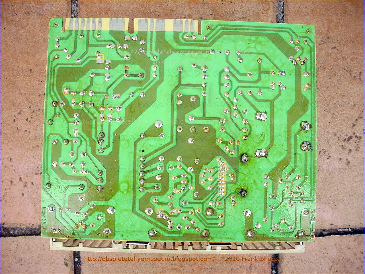


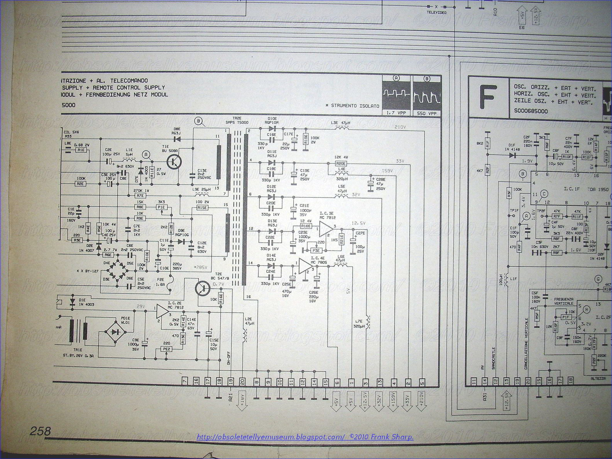


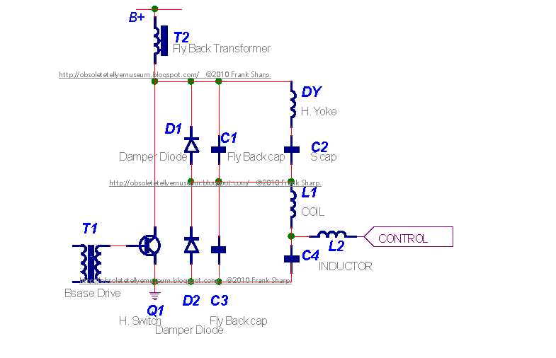


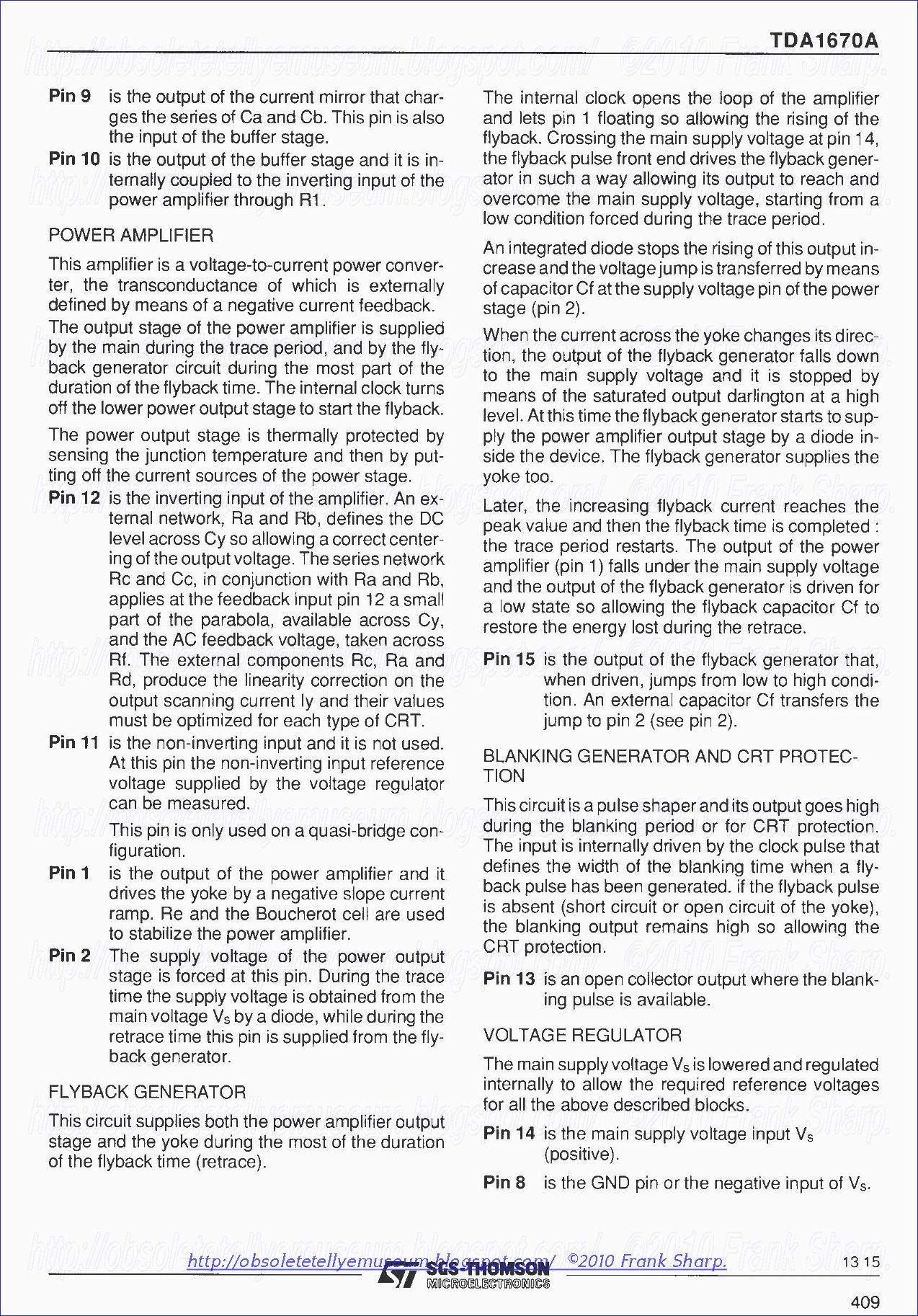


