

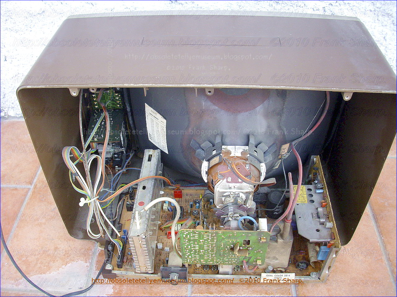


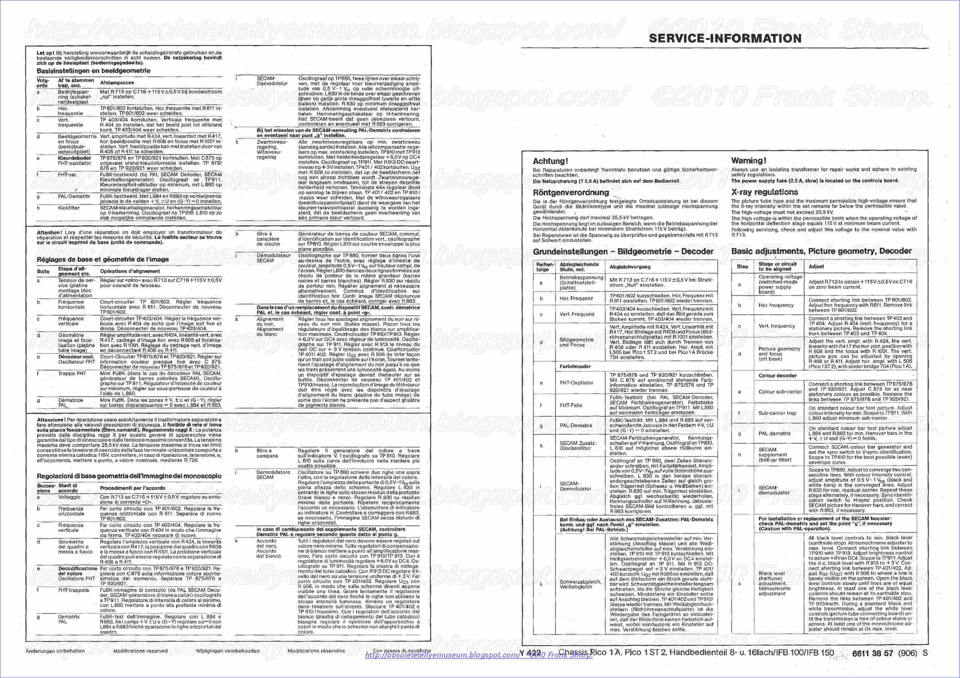


 ITT IDEAL COLOR 3214 OSCAR CHASSIS PICO 1A CIRCUIT ARRANGEMENT IN A
PICTURE DISPLAY DEVICE UTILIZING A STABILIZED SUPPLY VOLTAGE CIRCUIT:
ITT IDEAL COLOR 3214 OSCAR CHASSIS PICO 1A CIRCUIT ARRANGEMENT IN A
PICTURE DISPLAY DEVICE UTILIZING A STABILIZED SUPPLY VOLTAGE CIRCUIT:
A stabilized supply voltage circuit for a picture display device comprising a chopper wherein the switching signal has the line frequency and is duration-modulated. The coil of the chopper constitutes the primary winding of a transformer a secondary winding of which drives the line output transistor so that the switching transistor of the chopper also functions as a driver for the line output stage. The oscillator generating the switching signal may be the line oscillator. In a special embodiment the driver and line output transistor conduct simultaneously and in order to limit the base current of the line output transistor a coil shunted by a diode is incorporated in the drive line of the line output transistor. Other secondary windings of the transformer drive diodes which conduct simultaneously with the efficiency diode of the chopper so as to generate further stabilized supply voltages.
 1. An electrical circuit
arrangement for a picture display device operating at a given line
scanning frequency, comprising a source of unidirectional voltage, an
inductor, first switching transistor means for periodically energizing
said inductor at said scanning frequency with current from said source,
an electrical load circuit coupled to said inductor and having applied
thereto a voltage as determined by the ratio of the ON and OFF periods
of said transistor, means for maintaining the voltage across said load
circuit at a given value comprising means for comparing the voltage of
said load circuit with a reference voltage, means responsive to
departures of the value of the load circuit voltage from the value of
said reference voltage for varying the conduction ratio of the ON and
OFF periods of said transistor thereby to stabilize said load circuit
voltage at the given value, a line deflection coil system for said
picture display device, means for energizing said line deflection coil
system from said load voltage circuit means, means for periodically
interrupting the energization of said line deflection coil comprising
second switching means and means coupled to said inductor for deriving
therefrom a switching current in synchronism with the energization
periods of said transistor and applying said switching
current to said switching means thereby to actuate the same, and means
coupled to said switching means and to said load voltage circuit for
producing a voltage for energizing said 2. A circuit as claimed in claim
1 wherein the duty cycle of said switching 3. A circuit as claimed in
claim 1 further comprising an efficiency first 4. A circuit as claimed
in claim 3 further comprising at least a second diode coupled to said
deriving means and to ground, and being poled to 5. A circuit as claimed
in claim 1 wherein said second switching means comprises a second
transistor coupled to said deriving means to conduct simultaneously with
said first transistor, and further comprising a coil coupled between
said driving means and said second transistor and a third diode shunt
coupled to said coil and being poled to conduct when said 6. A circuit
as claimed in claim 1 further comprising a horizontal oscillator coupled
to said first transistor, said oscillator being the 7. A circuit as
claimed in claim 1 further comprising means coupled to said inductor for
deriving filament voltage for said display device.
1. An electrical circuit
arrangement for a picture display device operating at a given line
scanning frequency, comprising a source of unidirectional voltage, an
inductor, first switching transistor means for periodically energizing
said inductor at said scanning frequency with current from said source,
an electrical load circuit coupled to said inductor and having applied
thereto a voltage as determined by the ratio of the ON and OFF periods
of said transistor, means for maintaining the voltage across said load
circuit at a given value comprising means for comparing the voltage of
said load circuit with a reference voltage, means responsive to
departures of the value of the load circuit voltage from the value of
said reference voltage for varying the conduction ratio of the ON and
OFF periods of said transistor thereby to stabilize said load circuit
voltage at the given value, a line deflection coil system for said
picture display device, means for energizing said line deflection coil
system from said load voltage circuit means, means for periodically
interrupting the energization of said line deflection coil comprising
second switching means and means coupled to said inductor for deriving
therefrom a switching current in synchronism with the energization
periods of said transistor and applying said switching
current to said switching means thereby to actuate the same, and means
coupled to said switching means and to said load voltage circuit for
producing a voltage for energizing said 2. A circuit as claimed in claim
1 wherein the duty cycle of said switching 3. A circuit as claimed in
claim 1 further comprising an efficiency first 4. A circuit as claimed
in claim 3 further comprising at least a second diode coupled to said
deriving means and to ground, and being poled to 5. A circuit as claimed
in claim 1 wherein said second switching means comprises a second
transistor coupled to said deriving means to conduct simultaneously with
said first transistor, and further comprising a coil coupled between
said driving means and said second transistor and a third diode shunt
coupled to said coil and being poled to conduct when said 6. A circuit
as claimed in claim 1 further comprising a horizontal oscillator coupled
to said first transistor, said oscillator being the 7. A circuit as
claimed in claim 1 further comprising means coupled to said inductor for
deriving filament voltage for said display device. 
 bilized with a substantially constant voltage, the coil constituting the primary winding of a transformer.
Such a circuit arrangement is known from German
"Auslegeschrift" 1.293.304. wherein a circuit arrangement is described
which has for its object to convert an input direct voltage which is
generated between two terminals into a different direct voltage. The
circuit employs a switch connected to the first terminal of the input
voltage and periodically opens and closes so that the input voltage is
converted into a pulsatory voltage. This pulsatory voltage is then
applied to a coil. A diode is arranged between the junction of the
switch and the coil and the second terminal of the input voltage whilst a
load and a charge capacitor in parallel thereto are arranged between
the other end of the coil and the second terminal of the input voltage.
The assembly operates in accordance with the known efficiency principle
i.e., the current supplied to the load flows alternately through the
switch and through the diode. The function of the switch is performed by
a switching transistor which is driven by a periodical pulsatory
voltage which saturates this transistor for a given part of the period.
Such a configuration is known under different names in the literature;
it will be referred to herein as a "chopper." A known advantage thereof,
is that the switching transistor must be able to stand a high voltage
or provide a great current but it need not dissipate a great power. The
output voltage of the chopper is compared with a constant reference
voltage. If the output voltage attempts to vary because the input
voltage and/or the load varies, a voltage causing a duration modulation
of the pulses is produced at the output of the comparison arrangement.
As a result the quantity of the energy stored in the coil varies and the
output voltage is maintained constant. In the German "Auslegeschrift"
referred to it is therefore an object to provide a stabilized supply
voltage device.
bilized with a substantially constant voltage, the coil constituting the primary winding of a transformer.
Such a circuit arrangement is known from German
"Auslegeschrift" 1.293.304. wherein a circuit arrangement is described
which has for its object to convert an input direct voltage which is
generated between two terminals into a different direct voltage. The
circuit employs a switch connected to the first terminal of the input
voltage and periodically opens and closes so that the input voltage is
converted into a pulsatory voltage. This pulsatory voltage is then
applied to a coil. A diode is arranged between the junction of the
switch and the coil and the second terminal of the input voltage whilst a
load and a charge capacitor in parallel thereto are arranged between
the other end of the coil and the second terminal of the input voltage.
The assembly operates in accordance with the known efficiency principle
i.e., the current supplied to the load flows alternately through the
switch and through the diode. The function of the switch is performed by
a switching transistor which is driven by a periodical pulsatory
voltage which saturates this transistor for a given part of the period.
Such a configuration is known under different names in the literature;
it will be referred to herein as a "chopper." A known advantage thereof,
is that the switching transistor must be able to stand a high voltage
or provide a great current but it need not dissipate a great power. The
output voltage of the chopper is compared with a constant reference
voltage. If the output voltage attempts to vary because the input
voltage and/or the load varies, a voltage causing a duration modulation
of the pulses is produced at the output of the comparison arrangement.
As a result the quantity of the energy stored in the coil varies and the
output voltage is maintained constant. In the German "Auslegeschrift"
referred to it is therefore an object to provide a stabilized supply
voltage device.
In the circuit arrangement according to the mentioned German "Auslegeschrift" the frequency of the load variations or a harmonic thereof is chosen as the frequency for the switching voltage. Particularly when the load fed by the chopper is the line deflection circuit of a picture display device, wherein thus the impedance of the load varies in the rhythm of the line frequency, the frequency of the switching voltage is equal to or is a multiple of the line frequency.
It
is to be noted that the chopper need not necessarily be formed as that
in the mentioned German "Auslegeschrift." In fact, it is known from
literature that the efficiency diode and the coil may be exchanged. It
is alternatively possible for the coil to be provided at the first
terminal of the input voltage whilst the switching transistor is
arranged between the other end and the second terminal of the input
voltage. The efficiency diode is then provided between the junction of
said end and the switching transistor and the load. It may be recognized
that for all these modifications a voltage is present across the
connections of the coil which voltage has the same frequency and the
same shape as the pulsatory switching voltage. The control voltage of a
line deflection circuit is a pulsatory voltage which causes the line
output transistor to be saturates and cut off alternately. The invention
is based on the recognition that the voltage present across the
connections of the coil is suitable to function as such a control
voltage and that the coil constitutes the primary of a transformer. To
this end the circuit arrangement according to the invention is
characterized in that
a secondary winding of the transformer drives the switching element
which applies a line deflection current to line deflection coils and by
which the voltage for the final anode of a picture display tube which
forms part of the picture display device is generated, and that the
ratio between the period during which the switching transistor is
saturated and the entire period, i.e., the switching transistor duty
cycle is between 0.3 and 0.7 during normal operation.
The invention is also based on the recognition that the duration modulation which is necessary to stabilize the supply voltage with the switching transistor does not exert influence on the driving of the line output transistor. This resides in the fact that in case of a longer or shorter cut-off period of the line output transistor the current flowing through the line deflection coils thereof is not influenced because of the efficiency diode current and transistor current are taken over or, in case of a special kind of transistor, the collector-emitter current is taken over by the base collector current and conversely. However, in that case the above-mentioned ratios of 0.3 : 0.7 should be taken into account since otherwise this take-over principle is jeopardized.
As will be further explained the use of the switching transistor as a driver for the line output transistor in an embodiment to be especially described hereinafter has the further advantage that the line output transistor automatically becomes non-conductive when this switching transistor is short circuited so that the deflection and the EHT for the display tube drop out and thus avoid damage thereof.
Due to the step according to the invention t
he
switching transistor in the stabilized supply functions as a driver for
the line deflection circuit. The circuit arrangement according to the
invention may in addition be equipped with a very efficient safety
circuit so that the reliability is considerably enhanced, which is
described in the U.S. Pat. No. 3,629,686. The invention is furthermore
based on the recognition of the fact that the pulsatory voltage present
across the connections of the coil is furthermore used and to this end
the circuit arrangement according to the invention is characterized in
that secondary windings of the transformer drive diodes which conduct
simultaneously with the efficiency diode so as to generate further
stabilized direct voltages, one end of said diodes being connected to
ground.
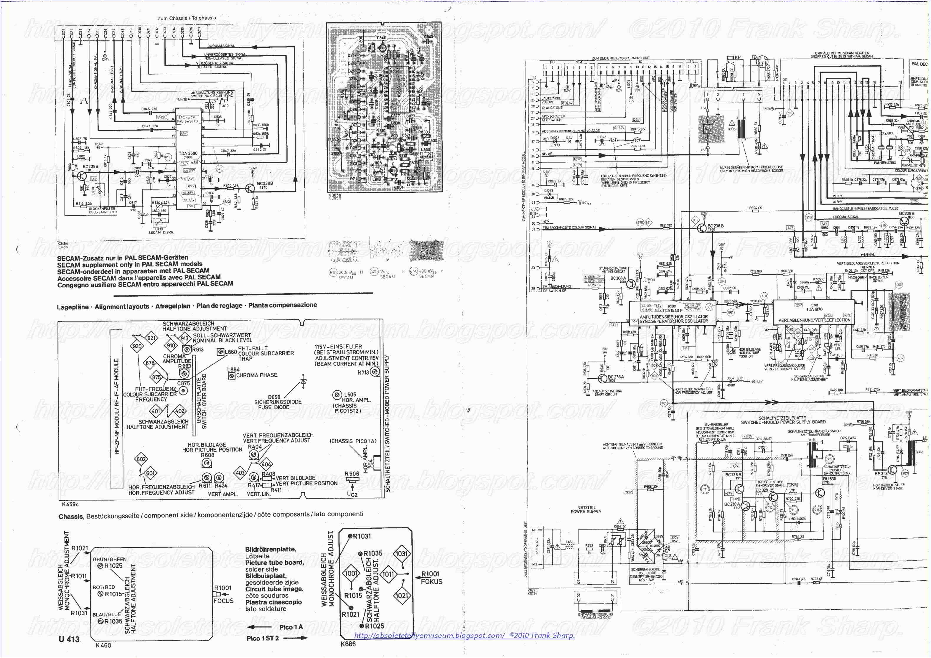
In order that the invention may be readily carried into effect, a few embodiments thereof will now be described in detail by way of example with reference to the accompanying diagrammatic drawings in which:
FIG. 1 shows a principle circuit diagram wherein the chopper and the line deflection circuit are further shown but other circuits are not further shown.
FIGS. 2a, 2b and 2c show the variation as a function of time of two currents and of a voltage occurring in the circuit arrangement according to FIG. 1.
FIGS. 3a 3b, 3c and 3d show other embodiments of the chopper.
FIGS. 4a and 4b show modifications of part of the circuit arrangement of FIG. 1.
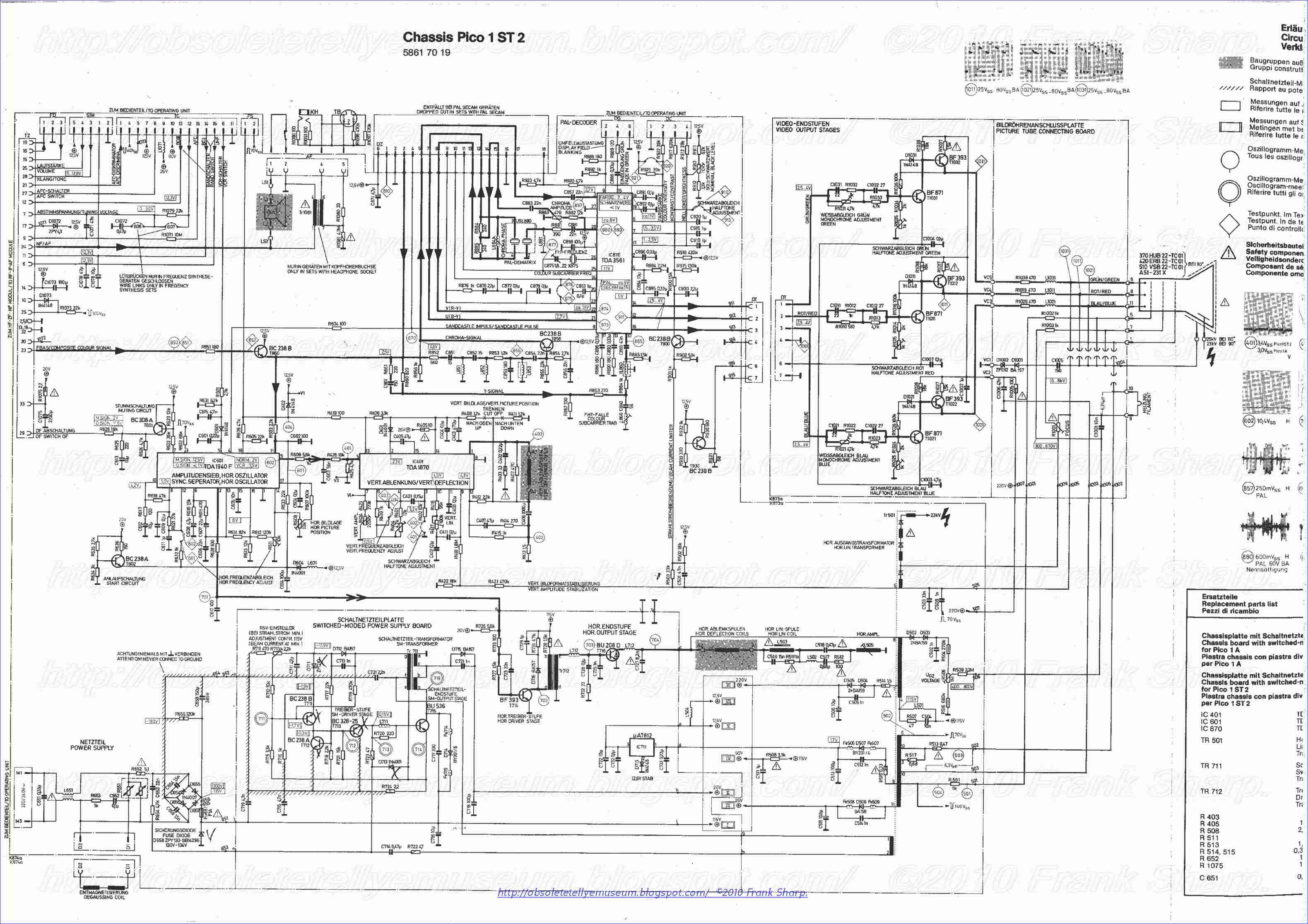
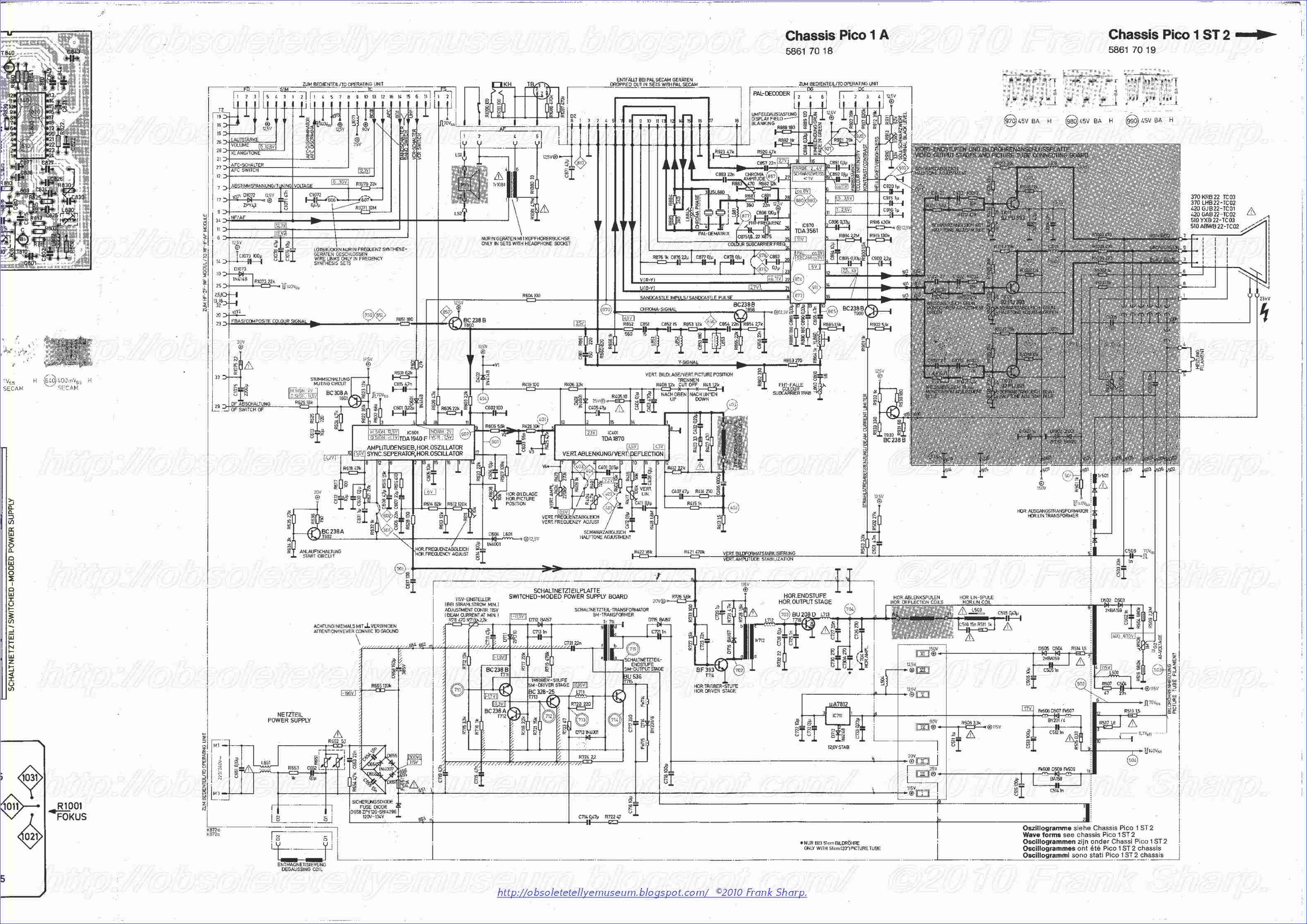
 In
FIG. 1 the reference numeral 1 denotes a rectifier circuit which
converts the mains voltage supplied thereto into a non-stabilized direct
voltage. The collector of a switching transistor 2 is connected to one
of the two terminals between which this direct voltage is obtained, said
transistor being of the npn-type in this embodiment and the base of
which receives a pulsatory voltage which originates through a control
stage 4 from a modulator 5 and causes transistor 2 to be saturated and
cut off alternately. The voltage waveform 3 is produced at the emitter
of transistor 2. In order to maintain the output voltage of the circuit
arrangement constant, the duration of the pulses provided is varied in
modulator 5. A pulse oscillator 6 supplies the pulsatory voltage to
modulator 5 and is synchronized by a signal of line frequency which
originates from the line oscillator 6' present in the picture display
device. This line oscillator 6' is in turn directly synchronized in
known manner by pulses 7' of line frequency which are present in the
device and originate for example from a received television signal if
the picture display device is a television receiver. Pulse oscillator 6
thus generates a pulsatory voltage the repetition frequency of which is
the line frequency.
The emitter of switching transistor 2 is connected at
one end to the cathode of an efficiency diode 7 whose other end is
connected to the second input voltage terminal and at the other end to
primary winding 8 of a transformer 9. Pulsatory voltage 3 which is
produced at the cathode of efficiency diode 7 is clamped against the
potential of said second terminal during the intervals when this diode
conducts. During the other intervals the pulsatory voltage 3 assumes the
value V i . A charge capacitor 10 and a load 11 are arranged
between the other end of winding 8 and the second input voltage
terminal. The elements 2,7,8,10 and 11 constitute a so-called chopper
producing a direct voltage across charge capacitor 10, provided that
capacitor 10 has a sufficiently great value for the line frequency and
the current applied to load 11 flowing alternately through switching
transistor 2 or through efficiency diode 7. The output voltage V o
which is the direct voltage produced across charge capacitor 10 is
applied to a comparison circuit 12 which compares the voltage V o with a reference voltage. Comparison circuit 12 generates a direct voltage which is applied
to modulator 5 so that the duration of the effective period δ T of
switching transistor 2 relative to the period T of pulses 3 varies as a
function of the variations of output voltage V 0 . In fact, it is readily evident that output voltage V o is proportional to the ratio δ :
In
FIG. 1 the reference numeral 1 denotes a rectifier circuit which
converts the mains voltage supplied thereto into a non-stabilized direct
voltage. The collector of a switching transistor 2 is connected to one
of the two terminals between which this direct voltage is obtained, said
transistor being of the npn-type in this embodiment and the base of
which receives a pulsatory voltage which originates through a control
stage 4 from a modulator 5 and causes transistor 2 to be saturated and
cut off alternately. The voltage waveform 3 is produced at the emitter
of transistor 2. In order to maintain the output voltage of the circuit
arrangement constant, the duration of the pulses provided is varied in
modulator 5. A pulse oscillator 6 supplies the pulsatory voltage to
modulator 5 and is synchronized by a signal of line frequency which
originates from the line oscillator 6' present in the picture display
device. This line oscillator 6' is in turn directly synchronized in
known manner by pulses 7' of line frequency which are present in the
device and originate for example from a received television signal if
the picture display device is a television receiver. Pulse oscillator 6
thus generates a pulsatory voltage the repetition frequency of which is
the line frequency.
The emitter of switching transistor 2 is connected at
one end to the cathode of an efficiency diode 7 whose other end is
connected to the second input voltage terminal and at the other end to
primary winding 8 of a transformer 9. Pulsatory voltage 3 which is
produced at the cathode of efficiency diode 7 is clamped against the
potential of said second terminal during the intervals when this diode
conducts. During the other intervals the pulsatory voltage 3 assumes the
value V i . A charge capacitor 10 and a load 11 are arranged
between the other end of winding 8 and the second input voltage
terminal. The elements 2,7,8,10 and 11 constitute a so-called chopper
producing a direct voltage across charge capacitor 10, provided that
capacitor 10 has a sufficiently great value for the line frequency and
the current applied to load 11 flowing alternately through switching
transistor 2 or through efficiency diode 7. The output voltage V o
which is the direct voltage produced across charge capacitor 10 is
applied to a comparison circuit 12 which compares the voltage V o with a reference voltage. Comparison circuit 12 generates a direct voltage which is applied
to modulator 5 so that the duration of the effective period δ T of
switching transistor 2 relative to the period T of pulses 3 varies as a
function of the variations of output voltage V 0 . In fact, it is readily evident that output voltage V o is proportional to the ratio δ :
V o = V i . δ
Load 11 of the chopper consists in the consumption of parts of the picture display device which are fed by output voltage V 0 . In a practical embodiment of the circuit arrangement according to FIG. 1 wherein the mains alternating voltage has a nominal effective value of 220 V and the rectified voltage V i is approximately 270 V, output voltage V o for δ = 0.5 is approximately 135 V. This makes it also possible, for example, to feed a line deflection circuit as is shown in FIG. 1 wherein load 11 then represents different parts which are fed by the chopper. Since voltage V o is maintained constant due to pulse duration modulation, the supply voltage of this line deflection circuit remains constant with the favorable result that the line amplitude(= the width of the picture displayed on the screen of the picture display tube) likewise remains constant as well as the EHT required for the final anode of the picture display tube in the same circuit arrangement independent of the variations in the mains voltage and the load on the EHT generator (= variations in brightness).
However,
variations in the line amplitude and the EHT may occur as a result of
an insufficiently small internal impedance of the EHT generator.
Compensation means are known for this purpose. A possibility within the
scope of the present invention is to use comparison circuit 12 for this
purpose. In fact, if the beam current passes through an element having a
substantially quadratic characteristic, for example, a
voltage-dependent resistor, then a variation for voltage V o
may be obtained through comparison circuit 12 which variation is
proportional to the root of the variation in the EHT which is a known
condition for the line amplitude to remain constant.
or example, at terminal 15
are generated in this manner at the amplitudes and polarities required
for the circuit arrangements present in the picture display device. In
FIG. 1 the voltage generated at terminal 15 is, for example, positive
relative to earth. It is to be noted that the load currents of the
supply voltages obtained in this manner cause a reduction of the
switching power which is economized by efficiency diode 7. The sum of
all diode currents including that of diode 7 is in fact equal to the
current which would flow through diode 7 if no secondary winding were
wound on transformer 9 and if no simultaneous diode were used. This
reduction may be considered an additional advantage of the circuit
arrangement according to the invention, for a diode suitable for smaller
powers may then be used. However, it will be evident that the overall
secondary load must not exceed the primary load since otherwise there is
the risk of efficiency diode 7 being blocked so that stabilization of
the secondary supply voltages would be out of the question.
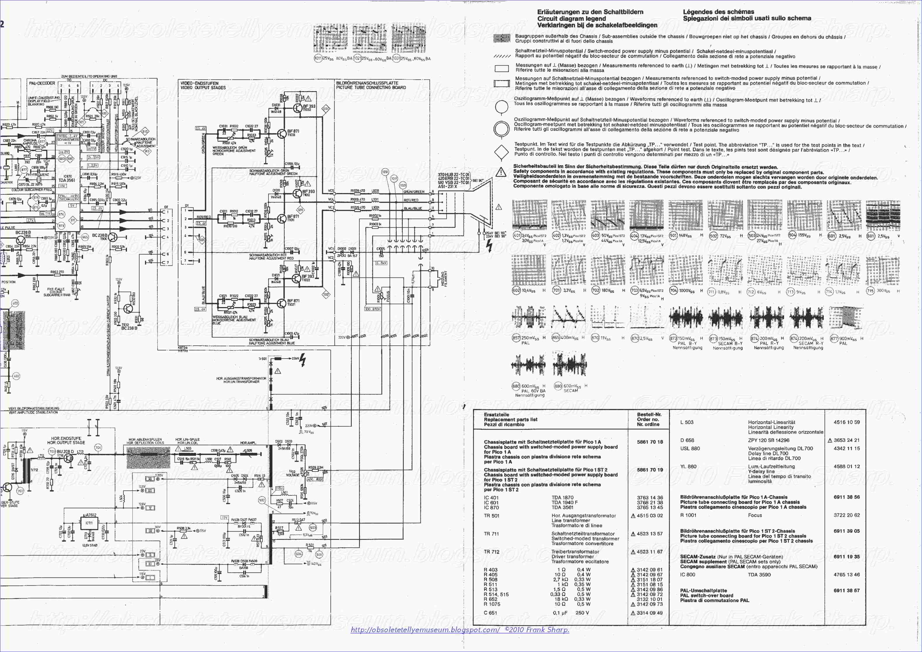
It is to be noted that a parabola voltage of line frequency as shown at 28 is produced across the charge capacitor 10 if this capacitor is given a smaller capacitance so that consequently the so-called S-correction is established.
In FIG. 1 charge capacitors are arranged between terminals 15 etc. and earth so as to ensure that the voltages on these points are stabilized direct voltages. If in addition the mean value of the voltage on one of these terminals has been made equal to the effective value of the alternating voltage which is required for heating the filament of the picture display tube present in the picture display device, this voltage is suitable for this heating. This is a further advantage of the invention since the cheap generation of a stabilized filament voltage for the picture display tube has always been a difficult problem in transistorized arrangements.
A further advantage of the picture display device according to the invention is that transformer 9 can function as a separation transformer so that the different secondary windings can be separated from the mains and their lower ends can be connected to ground of the picture display device. The latter step makes it possible to connect a different apparatus such as, for example, a magnetic recording and/or playback apparatus to the picture display device without earth connection problems occurring.
In FIG. 1 the reference numeral 14 denotes a secondary winding of transformer 9 which in accordance with the previously mentioned recognition of the invention can drive line output transistor 16 of the line deflection circuit 17. Line deflection circuit 17 which is shown in a simplified form in FIG. 1 includes inter alia line deflection coils 18 and an EHT transformer 19 a secondary winding 20 of which serves for generating the EHT required for the acceleration anode of the picture display tube. Line deflection circuit 17 is fed by the output voltage V o of the chopper which voltage is stabilized due to the pulse duration modulation with all previously mentioned advantages. Line deflection circuit 17 corresponds, for example, to similar arrangements which have been described in U.S. Pat. No. 3,504,224 issued Mar. 31, 1970 to J.J. Reichgelt et al., U.S. patent application Ser. No. 737,009 filed June 14, 1968 by W. H. Hetterscheid and U.S. application Ser. No. 26,497 filed April 8, 1970 by W. Hetterscheid et al. It will be evident that differently formed lined deflection circuits are alternatively possible.
It will now be shown that secondary winding 14 can indeed drive a line deflection circuit so that switching transistor 2 can function as a driver for the line deflection. FIGS. 2a and b show the variation as a function of time of the current i C which flows in the collector of transistor 16 and of the drive voltage v 14 across the terminals of secondary winding 14. During the flyback period (0, t 1 ) transistor 16 must be fully cut off because a high voltage peak is then produced at its collector; voltage v 14 must then be absolutely negative. During the scan period (t 1
, t 4 ) a sawtooth current i C
flows through the collector electrode of transistor 16 which current is
first negative and then changes its direction. As the circuit
arrangement is not free from loss, the instant t 3 when current i C becomes zero lies, as is known, before the middle of the scan period. At the end t 4
of the scan period transistor 16 must be switched off again. However,
since transistor 16 is saturated during the scan period and since this
transistor must be suitable for high voltages and great powers so that
its collector layer is thick, this transistor has a very great excess of
charge carriers in both its base and collector layers. The removal of
these charge carriers takes a period t s which is not
negligible whereafter the transistor is indeed switched off. Thus the
fraction δ T of the line period T at which v 14 is positive must end at the latest at the instant (t 4 - t s ) located after the commencement (t = 0) of the previous flyback.
The time δ T may be initiated at any instant t 2 which is located between the end t 1 of the flyback period and the instant t 3 when collector current i C reverses its direction. It is true that emitter current flows through transistor 16 at the in
stant t 2 , but collector current i C is not influenced thereby, at least not when the supply voltage (= V o )
for line deflection circuit 17 is high enough. All this has been
described in the U.S. Pat. No. 3,504,224. The same applies to line
deflection circuits wherein the collector base diode does not function
as an efficiency diode as is the case in the described circuit 17, but
wherein an efficiency diode is arranged between collector and emitter of
the line output transistor. In such a case the negative part of the
current i C of FIG. 2a represents the current flowing through the said efficiency diode.
After the instant t 3 voltage v 14 must be positive. In other words, the minimum duration of the period T when voltage v 14 must be positive is (t 4 - t s ) - t 3 whilst the maximum duration thereof is (t 4 - t s ) - t 1 . In a television system employing 625 lines per raster the line period t 4 is approximately 64 μus and the flyback period is approximately 12 μus. Without losses in the circuit arrangement instant t 3 would be located approximately 26 μus after the instant t 1 , and with losses a reasonable value is 22 μus which is 34 μus after the commencement of the period. If for safety's sake it is assumed that t s lasts approximately
10
μus, the extreme values of δ T are approximately 20 and 42 μus and
consequently the values for δ are approximately 0.31 and 0.66 at a mean
value which is equal to approximately 0.49. It was previously stated
that a mean value of δ = 0.5 was suitable. Line deflection circuit 17
can therefore indeed be used in combination with the chopper in the
manner described, and the relative variation of δ may be (0.66 - 0.31) :
0.49 = 71.5 percent. This is more than necessary to obviate the
variations in the mains voltage or in the various loads and to establish
the East-West modulation and ripple compensation to be described
hereinafter. In fact, if it is assumed that the mains voltage varies
between -15 and +10 percent of the nominal value of 220 V, while the 50
Hz ripple voltage which is superimposed on the input voltage V i has a peak-to-peak value of 40 V and V i is nominally 270 V, then the lowest occurring V i is:
0.85 × 270 V - 20 V = 210 V and the highest occurring V i is
1.1 × 270 V + 20 V = 320 V. For an output voltage V o of 135 V the ratio must thus vary between
δ = 135 : 210 = 0.64 and δ = 135 : 320 = 0.42.
A considerable problem presenting itself is that of
the simultaneous or non-simultaneous drive of line output transistor 16
with switching transistor 2, it being understood that in case of
simultaneous drive both transistors are simultaneously bottomed, that is
during the period δ T. This depends on the winding sense of secondary
winding 14 relative to that of primary winding 8. In FIG. 1 it has been
assumed that the drive takes place simultaneously so that the voltage
present across winding 14 has the shape shown in FIG. 2b. This voltage
assumes the value n(V i - V o ) in the period δ T
and the value -nVo in the period (1 - δ )T, wherein n is the ratio of
the number of turns on windings 14 and 8 and wherein V o is maintained constant at nominal mains voltage V o = δ V inom . However, if as a result of an increase or a decrease of the mains voltage V i increases or decreases proportionally therewith, i.e., V i = V i nom + Δ V, the positive portion of V 14 becomes equal to n(V i nom - V o +Δ V) = n [(1 -δ)V i nom +ΔV] = n(0.5 V inom +ΔV) if δ = 0.5 for V i = V i nom. Relatively, this is a variation which is twice as great. For example, if V i nom = 270 V and V o = 135 V, a variation in the mains voltage of from -15 to +10 percent causes a variation of V i
of from -40.5 V to +27 V which ranges from -30 to +20 percent of 135 V
which is present across winding 8 during the period δ T. The result is
that transistor 16 can always be bottomed over a large range of
variation. If the signal of FIG. 2b would be applied through a resistor
to the base of transistor 16, the base current thereof
would have to undergo the same variation while the transistor would
already be saturated in case of too low a voltage. In this case it is
assumed that transformer 9 is ideal (without loss) and that coil 21 has a
small inductance as is explained in the U.S. patent application Ser.
No. 737,009 above mentioned. It is therefore found to be desirable to
limit the base current of transistor 16.
This may be effected by providing a coil 22 having a large value inductance, approximately 100 μH, between winding 14 and the small coil 21. The variation of said base current i b is shown in FIG. 2c but not to the same scale as the collector current of FIG. 2a. During the conducting interval δ T current i b varies as a linear function of time having a final value of wherein L represents the inductance of coil 22. This not only provides the advantage that this final value is not immediately reached, but it can be shown that variation of this final value as a function of the mains voltage has been reduced, for there applies at nominal mains voltage that: If the mains voltage V i = V i nom +Δ V, then ##SPC1## because V i nom = 2 V o . Thus this variation is equal to that of the mains voltage and is not twice as great.
 During switching off, t 2 ,
of transistor 16 coil 22 must exert no influence and coil 21 must exert
influence which is achieved by arranging a diode 23 parallel to coil
22. Furthermore the control circuit of transistor 16 in this example
comprises the two diodes 24 and 25 as described in U.S. application Ser.
No. 26,497 above referred to, wherein one of these diodes, diode 25 in
FIG. 1, must be shunted by a resistor.
During switching off, t 2 ,
of transistor 16 coil 22 must exert no influence and coil 21 must exert
influence which is achieved by arranging a diode 23 parallel to coil
22. Furthermore the control circuit of transistor 16 in this example
comprises the two diodes 24 and 25 as described in U.S. application Ser.
No. 26,497 above referred to, wherein one of these diodes, diode 25 in
FIG. 1, must be shunted by a resistor.
The control circuit of transistor 16 may alternatively be formed as is shown in FIG. 4. In fact, it is known that coil 21 may be replaced by the parallel arrangement of a diode 21' and a resistor 21" by which the inverse current can be limited. To separate the path of the inverse current from that of the forward current the parallel arrangement of a the diode 29' and a resistor 29" must then be present. This leads to the circuit arrangement shown in the upper part of FIG. 4. This circuit arrangement may now be simplified if it is noted that diodes 25 and 21' on the one hand and diodes 23 and 29' on the other hand are series-arranged. The result is shown in the lower part of FIG. 4 which, as compared with the circuit arrangement of FIG. 1, employs one coil less and an additional resistor.
FIG. 3 shows possible modifications of the chopper. FIG. 3a shown in a simplified form the circuit arrangement according to FIG. 1 wherein the pulsatory voltage present across the connections of windings 8 has a peak-to-peak amplitude of V i - V o = 0.5 V i for δ = 0.5, As has been stated, the provision of coil 22 gives a relative variation for the base current of transistor 16 which is equal to that of the mains voltage. In the cases according to FIG. 3b, 3c and 3d the peak-to-peak amplitude of the voltage across winding 8 is equal to V i so that the provision of coil 22 results in a relative variation which is equal to half that of the mains voltage which is still more favorable than in the first case.
Transistors
of the npn type are used in FIG. 3. If transistors of the pnp type are
used, the relevant efficiency diodes must of course be reversed.
In this connection it is to be noted that it is possible to obtain an output voltage V o with the aid of the modifications according to FIGS. 3b, c and d, which voltage is higher than input voltage V i . These modifications may be used in countries such as, for example, the United of America or France where the nominal mains voltage is 117 or 110 V without having to modify the rest of the circuit arrangement.
The above-mentioned remark regarding the sum of the diode currents only applies, however, for the modifications shown in FIGS. 3a and d.
If line output transistor 16 is not simultaneously driven with switching transistor 2, efficiency diodes 7 conducts simultaneously with transistor 16 i.e., during the period which is denoted by δ T in FIGS. 1 and 2b. During that period the output voltage V o of the chopper is stabilized so that the base current of transistor 16 is stabilized without further difficulty. However, a considerable drawback occurs. In FIG. 1 the reference numeral 26 denotes a safety circuit the purpose of which is to safeguard switching transistor 2 when the current supplied to load 11 and/or line deflection circuit 17 becomes to high, which happens because the chopper stops. After a given period output voltage V o is built up again, but gradually which means that the ratio δ
is initially small in the order of 0.1. All this is described in U.S.
patent No. 3,629,686. The same phenomenon occurs when the display device
is switched on. Since δ = 0.1 corresponds to approximately 6 μs when T =
64 μs, efficiency diode 7 conducts in that case for 64 - 6 = 58 μus so
that transistor 16 is already switched on at the end of the scan or at a
slightly greater ratio δ during the flyback. This would cause an
inadmissibly high dissipation. For this reason the simultaneous drive is
therefore to be preferred.
The line deflection circuit itself is also safeguarded: in fact, if something goes wrong in the supply, the driver voltage of the line deflection circuit drops out because the switching voltage across the terminals of primary winding 8 is no longer present so that the deflection stops. This particularly happens when switching transistor 2 starts to constitute a short-circuit between emitter and collector with the result that the supply voltage V o for the line deflection circuit in the case of FIG. 1 becomes higher, namely equal to V i . However, the line output transformer is now cut off and is therefore also safe as well as the picture display tube and other parts of the display device which are fed by terminal 15 or the like. However, this only applies to the circuit arrangement according to FIG. 1 or 3a.
 Pulse
oscillator 6 applies pulses of line frequency to modulator 5. It may be
advantageous to have two line frequency generators as already
described, to wit pulse oscillator 6 and line oscillator 6' which is
present in the picture display device and which is directly synchronized
in known manner by line synchronizing pulses 7'. In fact, in this case
line oscillator 6' applies a signal of great amplitude and free from
interference to pulse oscillator 6. However, it is alternatively
possible to combine pulse oscillator 6 and line oscillator 6' in one
single oscillator 6" (see FIG. 1) which results in an economy of
components. It will be evident that line oscillator 6' and oscillator 6"
may alternatively be synchronized indirectly, for example, by means of a
phase discriminator. It is to be noted neither pulse oscillator 6, line
oscillator 6' and oscillator 6" nor modulator 5 can be fed by the
supply described since output voltage V o is still not
present when the mains voltage is switched on. Said circuit arrangements
must therefore be fed directly from the input terminals. If as
described above these circuit arrangements are to be separated from the
mains, a small separation transformer can be used whose primary winding
is connected between the mains voltage terminals and whose secondary
winding is connected to ground at one end and controls a rectifier at
the other end.
Capacitor 27 is arranged parallel to efficiency diode 7
so as to reduce the dissipation in switching transistor 2. In fact, if
transistor 2 is switched off by the pulsatory control voltage, its
collector current decreases and its collector-emitter voltage increases
simultaneously so that the dissipated power is not negligible before the
collector current has becomes zero. If efficiency diode 7 is shunted by
capacitor 27 the increase of the collector-emitter voltage is delayed
i.e., this voltage does not assume high values until the collector
current has already been reduced. It is true that in that case the
dissipation in transistor 2 slightly increases when it is switched on by
the pulsatory control voltage but on the other hand since the current
flowing through diode 7 has decreased due to the presence of the
secondary windings, its inverse current is also reduced when transistor 2
is switched on and hence its dissipation has become smaller. In
addition it is advantageous to delay these switching-on and
switching-off periods to a slight extent because the switching pulses
then contain fewer Fourier components of high frequency which may cause
interferences in the picture display device and which may give rise to
visible interferences on the screen of the display tube. These
interferences occupy a fixed position on the displayed image because the
switching frequency is the line frequency which is less disturbing to
the viewer. In a practical circuit wherein the line frequency is 15,625
Hz and wherein switching transistor 2 is an experimental type suitable
for a maximum of 350 V collector-emitter
voltage or 1 A collector current and wherein efficiency diode 7 is of
the Philips type BA 148 the capacitance of capacitor 27 is approximately
680 pF whilst the load is 70 W on the primary and 20 W on the secondary
side of transformer 9. The collector dissipation upon switching off is
0.3 W (2.5 times smaller than without capacitor 27) and 0.7 W upon
switching on.
Pulse
oscillator 6 applies pulses of line frequency to modulator 5. It may be
advantageous to have two line frequency generators as already
described, to wit pulse oscillator 6 and line oscillator 6' which is
present in the picture display device and which is directly synchronized
in known manner by line synchronizing pulses 7'. In fact, in this case
line oscillator 6' applies a signal of great amplitude and free from
interference to pulse oscillator 6. However, it is alternatively
possible to combine pulse oscillator 6 and line oscillator 6' in one
single oscillator 6" (see FIG. 1) which results in an economy of
components. It will be evident that line oscillator 6' and oscillator 6"
may alternatively be synchronized indirectly, for example, by means of a
phase discriminator. It is to be noted neither pulse oscillator 6, line
oscillator 6' and oscillator 6" nor modulator 5 can be fed by the
supply described since output voltage V o is still not
present when the mains voltage is switched on. Said circuit arrangements
must therefore be fed directly from the input terminals. If as
described above these circuit arrangements are to be separated from the
mains, a small separation transformer can be used whose primary winding
is connected between the mains voltage terminals and whose secondary
winding is connected to ground at one end and controls a rectifier at
the other end.
Capacitor 27 is arranged parallel to efficiency diode 7
so as to reduce the dissipation in switching transistor 2. In fact, if
transistor 2 is switched off by the pulsatory control voltage, its
collector current decreases and its collector-emitter voltage increases
simultaneously so that the dissipated power is not negligible before the
collector current has becomes zero. If efficiency diode 7 is shunted by
capacitor 27 the increase of the collector-emitter voltage is delayed
i.e., this voltage does not assume high values until the collector
current has already been reduced. It is true that in that case the
dissipation in transistor 2 slightly increases when it is switched on by
the pulsatory control voltage but on the other hand since the current
flowing through diode 7 has decreased due to the presence of the
secondary windings, its inverse current is also reduced when transistor 2
is switched on and hence its dissipation has become smaller. In
addition it is advantageous to delay these switching-on and
switching-off periods to a slight extent because the switching pulses
then contain fewer Fourier components of high frequency which may cause
interferences in the picture display device and which may give rise to
visible interferences on the screen of the display tube. These
interferences occupy a fixed position on the displayed image because the
switching frequency is the line frequency which is less disturbing to
the viewer. In a practical circuit wherein the line frequency is 15,625
Hz and wherein switching transistor 2 is an experimental type suitable
for a maximum of 350 V collector-emitter
voltage or 1 A collector current and wherein efficiency diode 7 is of
the Philips type BA 148 the capacitance of capacitor 27 is approximately
680 pF whilst the load is 70 W on the primary and 20 W on the secondary
side of transformer 9. The collector dissipation upon switching off is
0.3 W (2.5 times smaller than without capacitor 27) and 0.7 W upon
switching on.
As is known the so-called pincushion distortion is produced in the picture display tubes having a substantially flat screen and large deflection angles which are currently used. This distortion is especially a problem in color television wherein a raster correction cannot be brought about by magnetic means. The correction of the so-called East-West pincushion distortion i.e., in the horizontal direction on the screen of the picture display tube can be established in an elegant manner with the aid of the circuit arrangement according to the invention. In fact, if the voltage generated by comparison circuit 12 and being applied to modulator 5 for duration-modulating pulsatory voltage 3 is modulated by a parabola voltage 28 of field frequency, pulsatory voltage 3 is also modulated thereby. If the power consumption of the line deflection circuit forms part of the load on the output voltage of the chopper, the signal applied to the line deflection coils is likewise modulated in the same manner. Conditions therefore are that the parabola voltage 28 of field frequency has a polarity such that the en
velope
of the sawtooth current of line frequency flowing through the line
deflection coils has a maximum in the middle of the scan of the field
period and that charge capacitor 10 has not too small an impedance for
the field frequency. On the other hand the other supply voltages which
are generated by the circuit arrangement according to the invention and
which might be hampered by this component of field frequency must be
smoothed satisfactorily.
A practical embodiment of the described example with the reference numerals given provides an output for the supply of approximately 85 percent at a total load of 90 W, the internal resistance for direct current loads being 1.5 ohms and for pulsatory currents being approximately 10 ohms. In case of a variation of ± 10 percent of the mains voltage, output voltage V o is stable within 0.4 V. Under the nominal circumstances the collector dissipation of switching transistor 2 is approximately 2.5 W.
Since the internal resistance of the supply is so small, it can be used advantageously, for example, at terminal 15 for supplying a class-B audio amplifier which forms part of the display device. Such an amplifier has the known advantages that its dissipation is directly proportional to the amplitude of the sound to be reproduced and that its output is higher than that of a class-A amplifier. On the other hand a class-A amplifier consumes a substantially constant power so that the internal resistance of the supply voltage source is of little importance. However, if this source is highly resistive, the supply voltage is modulated in the case of a class-B amplifier by the audio information when the sound intensity is great which may detrimentally influence other parts of the display device. This drawback is prevented by means of the supply according to the invention.
The 50 Hz ripple voltage which is superimposed on the rectified input voltage V i
is compensated by comparison circuit 12 and modulator 5 since this
ripple voltage may be considered to be a variation of input voltage V i .
A further compensation is obtained by applying a portion of this ripple
voltage with suitable polarity to comparison circuit 12. It is then
sufficient to have a lower value for the smoothing capacitor which forms
part of rectifier circuit 1 (see FIG. 3). The parabola voltage 28 of
field frequency originating from the field time base is applied to the
same circuit 12 so as to correct the East-West pincushion distortion. 
ITT IDEAL COLOR 3214 OSCAR CHASSIS PICO 1A Synchronized switch-mode power supply:
In a switch mode power supply, a first switching transistor is coupled to a primary winding of an isolation transformer. A second switching transistor periodically applies a low impedance across a second winding of the transformer that is coupled to an oscillator for synchronizing the oscillator to the horizontal frequency. A third winding of the transformer is coupled via a switching diode to a capacitor of a control circuit for developing a DC control voltage in the capacitor that varies in accordance with a supply voltage B+. The control voltage is applied via the transformer to a pulse width modulator that is responsive to the oscillator output signal for producing a pulse-width modulated control signal. The control signal is applied to a mains coupled chopper transistor for generating and regulating the supply voltage B+ in accordance with the pulse width modulation of the control signal.
Description:
The invention relates to switch-mode power supplies.
Some television receivers have signal terminals for receiving, for example, external video input signals such as R, G and B input signals, that are to be developed relative to the common conductor of the receiver. Such signal terminals and the receiver common conductor may be coupled to corresponding signal terminals and common conductors of external devices, such as, for example, a VCR or a teletext decoder.
To simplify the coupling of signals between the
external devices and the television receiver, the common conductors of
the receiver and of the external devices are connected together so that
all are at the same potential. The signal lines of each external device
are coupled to the corresponding signal terminals of the receiver. In
such an arrangement, the common conductor of each device, such as of the
television receiver, may be held "floating", or conductively isolated,
relative to the corresponding AC mains supply source that energizes the
device. When the common conductor is held floating, a user touching a
terminal that is at the potential of the common conductor will not
suffer an electrical shock.
Therefore, it may be desirable to isolate the common conductor, or ground, of, for example, the television receiver from the potentials of the terminals of the AC mains supply source that provide power to the television receiver. Such isolation is typically achieved by a transformer. The isolated common conductor is sometimes referred to as a "cold" ground conductor.
In
a typical switch mode power supply (SMPS) of a television receiver the
AC mains supply voltage is coupled, for example, directly, and without
using transformer coupling, to a bridge rectifier. An unregulated direct
current (DC) input supply voltage is produced that is, for example,
referenced to a common conductor, referred to as "hot" ground, and that
is conductively isolated from the cold ground conductor. A pulse width
modulator controls the duty cycle of a chopper transistor switch that
applies the unregulated supply voltage across a primary winding of an
isolating flyback transformer. A flyback voltage at a frequency that is
determined by the modulator is developed at a secondary winding of the
transformer and is rectified to produce a DC output supply voltage such
as a voltage B+ that energizes a horizontal deflection circuit of the
television receiver. The primary winding of the flyback transformer is,
for example, conductively coupled to the hot ground conductor. The
secondary winding of the flyback transformer and voltage B+ may be
conductively isolated from the hot ground conductor by the hot-cold
barrier formed by the transformer.
It may be desirable to synchronize the operation of the chopper transistor to horizontal scanning frequency for preventing the occurrence of an objectionable visual pattern in an image displayed in a display of the television receiver.
It may be further desirable to couple a horizontal synchronizing signal that is referenced to the cold ground to the pulse-width modulator that is referenced to the hot ground such that isolation is maintained.
A synchronized switch mode power supply, embodying an
aspect of the invention, includes a transfromer having first and second
windings. A first switching arrangement is coupled to the first winding
for generating a first switching current in the first winding to
periodically energize the second winding. A source of a synchronizing
input signal at a frequency that is related to a deflection frequency is
provided. A second switching arrangement responsive to the input signal
and coupled to the second winding periodically applies a low impedance
across the energized second winding that by transformer action produces a
substantial increase in the first switching current. A periodic first
control signal is generated. The increase in the first switching current
is sensed to synchronize the first control signal to the input signal.
An output supply voltage is generated from an input supply voltage in
accordance with the first control signal.
ITT TDA1940, Line Circuits for TV Receivers (18-Pin Plastic Package)
These integrated circuits are advanced versions of the well-known types TDA1940, TDA1940F, TDA1950 and TDA1950F are identical
TBA940/950,
TDA9400/9500 etc. integrated line oscillator circuits. except the
following: at pin 2 the types having the suffix "F" supply ,
They
comprise all stages for sync separation and line synchronisation
horizontal output pulses of longer duration compared with the basic I
in
TV receivers in one single silicon chip. Due to their high degree of
types Integration, the number of external components is very small.
This
integrated circuit contains the horizontal sweep generator (HO), the
amplitude filter (AS), the sync-signal separating circuit (SA) and
the frequency/phase comparator (FP). For the purpose of suppressing
noise pulses which are caused via the operating voltage during the
upper and the lower inversion point of the horizontal sweep generator
(HO) which contains a single capacitor (C) and a first threshold
stage circuit (SS1) with two fixed thresholds, there are provided a
second and a third threshold stage circuit (SS2, SS3), to the inputs
of which the sawtooth signal is applied, and with the thresholds
thereof, approximately 2 μs prior to reaching the upper or the lower
peak value of the sawtooth signal, are being passed through thereby.
The output signal of the second threshold circuit (SS2) and the
output signal of the third threshold stage circuit (SS3) which is
applied via the pulse shaper circuit (IF), are superimposed linearly
and, via the stopper circuit (blocking stage) (SP) serve to control
the application of the composite video signal (BAS) to the amplitude
filter (AS), or else they are applied to a clamping circuit which
serves to apply the operating points of the amplitude filter (AS)
and/or of the sync-signal separating circuit (SA) to such a potential
that these two stages, for the time duration of these output pulses,
are prevented from operating.
1. An integrated circuit for
color television receivers, comprising a voltage- or
current-controlled horizontal sweep generator (HO), an amplitude
filter (AS), a synchronizing-signal separating circuit (SA) and a
frequency/phase comparator (FP) which serves to synchronize the
horizontal sweep generator (HO), with said generator being a sawtooth
generator containing a single capacitor
(C) and a first threshold stage circuit (SS1) having two fixed thresholds, said integrated circuit further comprising: a second and a third threshold stage circuit (SS2, SS3) each being supplied with the sawtooth signal on the input side, comprising each time one threshold which, approximately 2μs prior to the reaching of the upper or the lower peak value of the sawtooth signal, is being passed thereby;
a pulse shaper circuit (IF) coupled to the output of said third threshold stage circuit (SS3) which pulse shaper circuit reduces the duration of the output pulse thereof to about the duration of the output pulse of said second threshold stage circuit (SS2), and
a stopper circuit (blocking stage) (SP) coupled to the outputs of both said pulse shaper circuit (IF) and said second threshold stage circuit (SS2), said stopper circuit having a signal input to which there is applied a composite video signal (BAS) and a signal output which is coupled to the input of said amplitude filter (AS).
2. The invention of claim 1 wherein the outputs of both said pulse shaper circuit (IF) and said second threshold stage circuit (SS2) are coupled to a clamping circuit which applies the operating points of said amplitude filter (AS) and said sync-separating signal (SA) to such a potential that they are prevented from operating.
3. An integrated horizontal sweep circuit comprising:
a generator for generating a sawtooth signal;
an amplitude filter having an input for receiving a composite video signal and having an output;
a sync-signal separating circuit having an input coupled to said amplitude filter output and having an output;
a frequency/phase comparator having a first input coupled to said separating circuit output,
a second input receiving said sawtooth signal and an output for controlling said generator; and
a control circuit responsive to said sawtooth signal for inhibiting said composite video signal when said sawtooth signal is within predetermined signal level ranges about the upper and lower inversion points of said sawtooth signal.
4. An integrated circuit in accordance with claim 3 wherein:
said generator comprises a capacitor, circuit means for charging and discharging said capacitor, and a first threshold circuit controlling said circuit means in response to said sawtooth signal reaching a first level corresponding to said first inversion point and a second level corresponding to said second inversion point.
5. An integrated horizontal sweep circuit comprising:
a sawtooth signal generator;
an amplitude filter having an input receiving a composite video signal and having an output;
a sync-signal separating circuit having an input coupled to said amplitude filter output and having an output;
a frequency/phase comparator having a first input coupled to said separating circuit output, a second input receiving said sawtooth signal and an output for controlling said generator; and
a control circuit responsive to said sawtooth signal for inhibiting operation of said amplitude filter and/or said sync-signal separating circuit when said sawtooth signal is within predetermined signal level ranges about the upper and lower inversion point of said sawtooth signal.
6. An integrated circuit in accordance with claim 5 wherein:
said generator comprises a capacitor, circuit means for charging and discharging said capacitor and a first threshold circuit controlling said circuit means in response to said sawtooth signal reaching a first level corresponding to said first inversion point and a second level corresponding to said second inversion point.
The invention relates to an integrated circuit for (color) television receivers, comprising a voltage- or current-controlled horizontal-sweep generator, an amplitude filter, a synchronizing signal separating circuit (sync-separator) and a frequency/phase comparator which serves to synchronize the horizontal sweep generato
 r which is a sawtooth
generator consisting of a single capacitor and of a first threshold
stage having two fixed switching thresholds, cf. preamble of the patent
claim. Such types of integrated circuits, for example, are known
from the technical journal "Elektronik aktuell", 1976, No. 2, pp. 7
to 14 where they are referred to as TDA 9400 and TDA 9500.
r which is a sawtooth
generator consisting of a single capacitor and of a first threshold
stage having two fixed switching thresholds, cf. preamble of the patent
claim. Such types of integrated circuits, for example, are known
from the technical journal "Elektronik aktuell", 1976, No. 2, pp. 7
to 14 where they are referred to as TDA 9400 and TDA 9500. Especially on account of the fact that the amplitude filter as well as the horizontal sweep generator in the form of the aforementioned sawtooth generator, are integrated on a single semiconductor body, it is likely that noise interference pulses coming from the individual stages, and via the supply voltage line, may have a disturbing influence upon the horizontal sweep generator, i.e. upon the threshold stage thereof, in such a way that either the lower or the upper or successively both switching thresholds are exceeded before the time by the voltage at the capacitor, owing to the noise superposition, so that the generator will show to have a "wrong" frequency or phase position. This frequency/phase variation, of course, is compensated for by the circuit, with the aid of the synchronzing pulses, but only in such a way that the noise effect remains visible in the television picture.
SUMMARY OF THE INVENTION
The invention is characterized in the claim is aimed at overcoming this drawback by solving the problem of designing an integrated circuit of the type described in greater detail hereinbefore, in such a way that noise pulses acting upon the capacitor voltage or the internal reference voltages for the switching thresholds (see below) in the proximity of the two switching thresholds, are prevented from having the described disadvantageous effect. Accordingly, an advantage of the invention results directly from solving the given problem.
Other objects, features and advantages of the present invention will become more fully apparent from the following detailed description of the preferred embodiment, the appended claims and the accompanying drawing in which:
BRIEF DESCRIPTION OF THE INVENTION
The invention will now be described in greater detail with reference to the accompanying drawing. This drawing, in the form of a schematical circuit diagram, shows the construction of an integrated circuit according to the invention.
DETAILED DESCRIPTION OF THE INVENTION
T
he
horizontal sweep generator HO comprises the capacitor C as connected
to the zero point of the circuit, and which is charged and
discharged via the two shown constant current sources CS1 and CS2,
thus causing the intended sawtooth voltage to appear thereat.
Moreover, the horizontal sweep generator HO comprises the first
threshold stage circuit SS1, having an upper and a lower threshold.
As soon as the capacitor voltage exceeds one of the thresholds, the
first threshold stage circuit SS1 switches over to the other
threshold. The two thresholds are defined by the voltage divider P as
connected to the operating voltage U, and in which the corresponding
threshold inputs are connected to corresponding tapping points. The
output of the threshold stage circuit SS1 controls the electronic
switch S, so that the constant current source CS2 as connected
thereto, is either disconnected from or connected to the zero point
of the circuit. Accordingly, in the disconnected state, the capacitor
C is charged via the constant current source CS1 arranged in series
therewith while in the connected state the capacitor C is discharged
across the aforementioned constant current source CS2 arranged in
parallel therewith, if, as a matter of fact, the current of the
constant current source CS1 arranged in series with the capacitor C,
is smaller than that of the parallel-arranged constant current source
CS2.
Now, for the purpose of avoiding the aforementioned
drawbacks, there is provided a second and a third threshold stage
circuit SS2 and SS3, respectively, as well as the pulse shaper circuit
IF. To the respective input of the two threshold stage circuits SS2,
SS3, there is applied the capacitor voltage, in the form of the
sawtooth signal, and these stages have a threshold voltage which,
approximately 2 μs prior to the reaching of the upper or the lower
peak value of the sawtooth voltage, is being passed thereby. This
means to imply that the threshold voltage of the second threshold
stage circuit SS2 is somewhat lower than the voltage of the upper
threshold of the first threshold stage circuit SS1, and that the
threshold voltage of the third threshold stage circuit SS3 is
somewhat higher than the voltage of the lower threshold of the first
threshold stage circuit SS1. The two thresholds of the threshold
stage circuits SS2, SS3 can thus be realized in a simple way by
providing further tapping points at the voltage divider P, as is
shown in the accompanying drawing. Thus, the second threshold stage
circuit SS2 is provided for at a voltage divider tapping point below
the tapping point chosen for the upper threshold, and the tapping
point for the third threshold stage circuit SS3 is provided for above
the tapping point which has been chosen for the lower threshold of
the first threshold stage circuit SS1.
Since, within the area
of the lower inversion point of the sawtooth signal there results an
excessively wide output pulse of the third threshold stage circuit
SS3, the pulse shaper circuit IF is arranged subsequently thereto,
for reducing the duration of the output pulse as applied to its
input, to about the duration of the output pulse of the second
threshold stage circuit SS2. This pulse shaper circuit IF, for
example, may be realized by a monoflop, in particular by a digital
monoflop (=monostable circuit).
The output pulses of the
second threshold stage circuit SS2 and of the pulse shaper circuit IF
are then super-positioned linearly, with this being denoted in the
drawing by a simple interconnection of the two respective lines. The
combined signal is applied to the input of the stopper circuit
(blocking stage) SP, to the signal input of which there is fed the
composite video signal BAS, and the output thereof controls both the
amplitude filter AS and the synchronizing signal separating circuit
SA.
The combined signal may also be used to control a
clamping circuit applying the operating points of the amplitude filter
AS and/or of the sync-signal-separating circuit SA to such a
potential which prevents it from operating.
If now the
sawtooth signal reaches the range of its upper or its lower inversion
point, the composite video signal BAS is not applied to either the
amplitude filter AS or the sync-signal separating circuit SA, so that
shortly before and shortly after the inversion points, signals are
prevented from being processed in the two stages AS, SA. This, in turn,
has the consequence that during these times noise pulses are
prevented from superimposing upon the operating voltage U, so that
there is also prevented an unintended triggering of the first
threshold stage circuit SS1.
Moreover, it is still shown in
the drawing that the amplitude filter AS, the sync-signal separating
circuit SA and the frequency/phase comparator FP are arranged in
series in terms of signal flow, with the latter, in addition,
receiving the sawtooth signal, and with the output signal thereof
acting upon the two current sources in a regulating sense. In the
drawing, this is indicated by the setting arrows at the two current
sources.
While the present invention has been disclosed in
connection with the preferred embodiment thereof, it should be
understood that there may be other embodiments which fall within the
spirit and scope of the invention as defined by the following claims.
TDA1870 - FRAME DEFLECTION
Form/Case/Outline: Multiwatt-15 (TDA1870A);
Type/Application: TV Vertical Deflection Unit.
Daten/electr.data: Vs max: 35 V; I15: 100 mA; Ptot: 30 W; Tmax j: 150 °C.
Varianten: TDA1670[A], TDA1675[A], TDA1872[A] -
The PHILIPS TDA3560A
is a decoder for the PAL colour television standard. It combines all functions required for the identification
and demodulation of PAL signals. Furthermore it contains a luminance amplifier, an RGB-matrix and amplifier. These
amplifiers supply output signals up to 5 V peak-to-peak (picture information) enabling direct drive of the discrete output
stages. The circuit also contains separate inputs for data insertion, analogue as well as digital, which can be used for
text display systems (e.g. (Teletext/broadcast antiope), channel number display, etc. Additional to the TDA3560, the
circuit includes the following features:
· The peak white limiter is only active during the time that the 9,3 V level at the output is exceeded. The start of the
limiting function is delayed by one line period. This avoids peak white limiting by test patterns which have abrupt
transitions from colour to white signals.
· The brightness control is obtained by inserting a variable pulse in the luminance channel. Therefore the ratio of
brightness variation and signal amplitude at the three outputs will be identical and independent of the difference in gain
of the three channels. Thus discolouring due to adjustment of contrast and brightness is avoided.
· Improved suppression of the internal RGB signals when the device is switched to external signals, and vice versa.
· Non-synchronized external RGB signals do not disturb the black level of the internal signals.
· Improved suppression of the residual 4,4 MHz signal in the RGB output stages.
· Cascoded stages in the demodulators and burst phase detector minimize the radiation of the colour demodulator
inputs.
· High current capability of the RGB outputs and the chrominance output.
APPLICATION INFORMATION
The function is described against the corresponding pin
number.
1. + 12 V power supply
The circuit gives good operation in a supply voltage range
between 8 and 13,2 V provided that the supply voltage for
the controls is equal to the supply voltage for the
TDA3561A. All signal and control levels have a linear
dependency on the supply voltage. The current taken by
the device at 12 V is typically 85 mA. It is linearly
dependent on the supply voltage.
2. Control voltage for identification
This pin requires a detection capacitor of about 330 nF for
correct operation. The voltages available under various
signal conditions are given in the specification.
3. Chrominance input
The chroma signal must be a.c.-coupled to the input.
Its amplitude must be between 55 mV and 1100 mV
peak-to-peak (25 mV to 500 mV peak-to-peak burst
signal). All figures for the chroma signals are based on a
colour bar signal with 75% saturation, that is the
burst-to-chroma ratio of the input signal is 1 : 2,25.
4. Reference voltage A.C.C. detector
This pin must be decoupled by a capacitor of about 330
nF. The voltage at this pin is 4,9 V.
5. Control voltage A.C.C.
The A.C.C. is obtained by synchronous detection of the
burst signal followed by a peak detector. A good noise
immunity is obtained in this way and an increase of the
colour for weak input signals is prevented. The
recommended capacitor value at this pin is 2,2 mF.
6. Saturation control
The saturation control range is in excess of 50 dB.
The control voltage range is 2 to 4 V. Saturation control is
a linear function of the control voltage.
When the colour killer is active, the saturation control
voltage is reduced to a low level if the resistance of the
external saturation control network is sufficiently high.
Then the chroma amplifier supplies no signal to the
demodulator. Colour switch-on can be delayed by proper
choice of the time constant for the saturation control
setting circuit.
When the saturation control pin is connected to the power
supply the colour killer circuit is overruled so that the colour
signal is visible on the screen. In this way it is possible to
adjust the oscillator frequency without using a frequency
counter (see also pins 25 and 26).
7. Contrast control
The contrast control range is 20 dB for a control voltage
change from + 2 to + 4 V. Contrast control is a linear
function of the control voltage. The output signal is
suppressed when the control voltage is 1 V or less. If one
or more output signals surpasses the level of 9 V the peak
white limiter circuit becomes active and reduces the output
signals via the contrast control by discharging C2 via an
internal current sink.
8. Sandcastle and field blanking input
The output signals are blanked if the amplitude of the input
pulse is between 2 and 6,5 V. The burst gate and clamping
circuits are activated if the input pulse exceeds a level of
7,5 V.
The higher part of the sandcastle pulse should start just
after the sync pulse to prevent clamping of video signal on
the sync pulse. The width should be about 4 ms for proper
A.C.C. operation.
9. Video-data switching
The insertion circuit is activated by means of this input by
an input pulse between 1 V and 2 V. In that condition, the
internal RGB signals are switched off and the inserted
signals are supplied to the output amplifiers. If only normal
operation is wanted this pin should be connected to the
negative supply. The switching times are very short
(< 20 ns) to avoid coloured edges of the inserted signals
on the screen.
10. Luminance signal input
The input signal should have a peak-to-peak amplitude of
0,45 V (peak white to sync) to obtain a black-white output
signal to 5 V at nominal contrast. It must be a.c.-coupled to
the input by a capacitor of about 22 nF. The signal is
clamped at the input to an internal reference voltage.
A 1 kW luminance delay line can be applied because the
luminance input impedance is made very high.
Consequently the charging and discharging currents of the
coupling capacitor are very small and do not influence the
signal level at the input noticeably. Additionally the
coupling capacitor value may be small.
ITT IDEAL COLOR 3214 OSCAR CHASSIS PICO 1A Video signal processing circuit for a color television receiver PHILIPS TDA3560: In a video signal processing circuit for a color television receiver, a
brightness setting, which is operative for external color signals as
well as for internal color signals and which does not produce a color
shift, can be obtained by combining with the luminance signal (Y) a
level shift signal (H) the amplitude of which is adjustable by the
brightness setting and by employing in each color channel two clamping
circuits, the first one of which clamps a first reference level (RL1)
in the external color signal (ER, EG, EB) onto a combination of the
level shift signal and the internal color signal (R, G, B) and the
second clamping circuit clamps a second reference leve (RL2)
which occurs in the sum signal of the internal and the external color
signal when the level shift signal has zero value, onto the cutoff level
of the relevant electron gun of a picture display tube.
1. A video signal
processing circuit for a color television receiver having inputs for a
luminance signal, for color difference signals and for external color
signals, comprising respective matrix circuits for combining the
respective color difference signals with the luminance signal to form
respective color signals, respective first clamping circuits for
clamping the respective external color signals onto the respective color
signals, respective combining circuits for combining the respective
clamped external color signals with the respective color signals,
respective second clamping circuits for clamping the outputs of the
respective combining circuits onto a predetermined level, and a
brightness setting circuit, characterized in that the first clamping
circuits act on a first reference level in said respective external
color signals occurring in a first group of periods and the second
clamping circuits act on a second reference level occurring in a second
group of periods which differ from the periods of the first group, while
the brightness setting circuit is an amplitude setting circuit for a
level shift signal, which is combined with the luminance signal prior to
processing the color difference signals, with which the relative
position of the second reference level with respect to the remaining
portion of the luminance signal is adjustable.
2. A video signal processing circuit as claimed in claim
1, characterized in that the respective first and second clamping
circuits are operative alternately and every other line flyback period.
The invention relates to a video signal processing circuit for a color television receiver having inputs for a luminance signal, for color difference signals, and for external color signals, comprising a matrix circuit for combining a color difference signal with the luminance signal to form a color signal, a first clamping circuit for clamping an external color signal onto the corresponding color signal, a combining circuit for combining a clamped external color signal with the corresponding color signal, a second clamping circuit acting on an output signal of the combining circuit and a brightness setting circuit.
A video
signal processing circuit of the type defined above is described in
Philip Data Handbook for Integrated Circuits, Part 2, May, 1980 as IC
TDA3560. The brightness setting, which is common for internal and
external video signals, is obtained by means of a common direct current
level setting of the second clamping circuits. The settings of the three
electron guns of a picture display tube coupled to the outputs of the
video signal processing circuit are changed to an equal extent by this
direct current level setting as a result whereof, due to the mutual
differences in the efficiency of the phosphors of the picture display
tube, a color shift may occur at a brightness adjustment. It is an
object of the invention to prevent this. SUMMARY OF THE INVENTION
According to the invention, a video signal processing circuit of the type defined in the preamble is therefore characterized in that the first clamping circuit acts on a first reference level occurring in a first group of periods and the second clamping circuit acts on a second reference level occurring in a second group of periods which differ from the periods of the first group, while the brightness setting circuit is an amplitude setting circuit for a level shift signal with which the relative position of the second reference level with respect to the remaining portion of the luminance signal is adjustable.
Owing to the measure in accordance with the invention, the common setting of the brightness for internal video signals is maintained and a color shift is prevented from occurring at a brightness setting.
DESCRIPTION OF THE DRAWINGS
An embodiment of the invention will now be further described by way of example with reference to the accompanying drawings.
In the drawings:
FIG. 1 illustrates, by means of a block schematic circuit diagram, a video signal processing circuit in accordance with the invention; and
FIG. 2 shows some waveforms such as they may occur in the circuit shown in FIG. 1.
DESCRIPTION OF THE PREFERRED EMBODIMENT
 In
FIG. 1, an external red color signal ER' is applied to an input 1, a
red color difference signal (R-Y) to an input 3, an external green color
signal EG' to an input 5, a luminance signal Y to an input 7, a green
color difference signal (G-Y) to an input 9, an external blue color
signal EB' to an input 11, a blue color difference signal (B-Y) to an
input 13 and a synchronizing signal S to an input 15.
In
FIG. 1, an external red color signal ER' is applied to an input 1, a
red color difference signal (R-Y) to an input 3, an external green color
signal EG' to an input 5, a luminance signal Y to an input 7, a green
color difference signal (G-Y) to an input 9, an external blue color
signal EB' to an input 11, a blue color difference signal (B-Y) to an
input 13 and a synchronizing signal S to an input 15. The luminance signal at the input 7 is shown in FIG. 2 as a waveform 207. In the line flyback periods this luminance signal has a black level Z which, for simplicity, is assumed to occur in all cases during the whole line flyback period but which may, of course, alternatively occur during only a portion of that line flyback period.
The luminance signal Y is applied to an input 17 of a combining circuit 19. To a further input 21 thereof, a level shift signal H is applied which, via an amplitude setting circuit 23, is obtained from an output 25 of a pulse generator 27, to an input 29 of which the synchronizing signal S is applied.
The level shift signal H is shown in FIG. 2 as a waveform 221 which in this case has a zero amplitude every other line flyback period and at other times an amplitude which depends on the setting of the amplitude setting circuit 23.
 The respective color
difference signals (R-Y), (G-Y) and (B-Y) at the respective inputs 3, 9
and 13, are applied to inputs 31, 33 and 35, respectively, of matrix
circuits 37, 39 and 41, respectively, to respective inputs 43, 45 and 47
of which the combination Y+H of the luminance signal (Y) and the level
shift signal (H) is applied, and from respective outputs 49, 51 and 53,
the red (R) and green (G) and blue (B) color signals are obtained. FIG. 2
shows the red color signal of said color signals as a waveform 249.
The respective color
difference signals (R-Y), (G-Y) and (B-Y) at the respective inputs 3, 9
and 13, are applied to inputs 31, 33 and 35, respectively, of matrix
circuits 37, 39 and 41, respectively, to respective inputs 43, 45 and 47
of which the combination Y+H of the luminance signal (Y) and the level
shift signal (H) is applied, and from respective outputs 49, 51 and 53,
the red (R) and green (G) and blue (B) color signals are obtained. FIG. 2
shows the red color signal of said color signals as a waveform 249. The respective external color signals ER', EG' and EB' at the respective inputs 1, 5 and 11 are applied to respective inputs 61, 63 and 65 of respective combining circuits 67, 69 and 71 via respective capacitors 55, 57 and 59. Further inputs 73, 75 and 77, respectively, of the combining circuits 67, 69 and 71, respectively, are connected to the outputs 49, 51 and 53, respectively, of the matrix circuits 37, 39 and 41, respectively, and receive the red, green and blue color signals, respectively.
Arranged between the inputs 61 and 73, 63 and 75, and 65 and 77, respectively, there are first clamping circuits 79, 81 and 83, respectively, which, under the control of a pulse signal K1 coming from an output 84 of the pulse generator 27, clamps a first reference level RL1 in the respective external color signals ER', EG' and EB' onto the respective color signals R, G and B, as a result of which the respective clamped external color signals ER, EG and EB at the respective inputs 61, 63 and 65 of the combining circuits 67, 69 and 71 are produced, the signal level ER at the input 61 of the combining circuit 67 being shown in FIG. 2 as the waveform 261. The pulse signal K1 is shown in FIG. 2 as the waveform 284.
At respective outputs 85, 87 and 89 of the combining circuits 67, 69 and 71, respectively, there are now produced signals which are the sums of the respective clamped external color signals ER, EG and EB and the respective color signals R, G and B. Via respective capacitors 91, 93 and 95, said sum signals (ER+R), (EG+G) and (EB+B), respectively, are applied to respective inputs 97, 99 and 100 of respective video output amplifiers 102, 104 and 106, respective outputs 108, 110 and 112 of which being connected to respective cathodes of a picture display tube 114.
Second clamping circuits 116, 118 and 120, respectively, which are rendered operative by a pulse signal K2 coming from an output 122 of the pulse generator 27 and whereby a second reference level RL2 in the signals at the respective inputs 97, 99 and 100 is adjusted to a fixed potential, zero potential here, are connected to the respective inputs 97, 99 and 100 of the respective video output amplifiers 102, 104 and 106. This is shown in FIG. 2 by means of the waveform 297 for the signal (ER+R) at the input 97 of the video output amplifier 102. For the sake of clearness, the luminance signal (Y) and the red color difference signal (R-Y) are assumed to have zero values.
The picture display tube 114 has a deflection circuit 124 which is controlled by signals coming from outputs 126 and 128, respectively, of the pulse generator 27.
On the basis of FIG. 2, it will now be demonstrated that the brightness of the color signals as well as of the external color signals is adjustable by means of the amplitude setting circuit 23, more specifically in such a ratio, occurring at the picture display tube 114, that no color shift is produced.
If a luminance signal Y and a color difference signal
(R-Y) are produced and the external color signal ER' has zero value, the
signal at the output 49 of the matrix circuit 37 has the waveform 249
and likewise the signal at the input 97 of the video output amplifier
108, as during the occurrence of the signal K2 (waveform 222), the
second clamping circuit 116 has adjusted the second reference level RL2
to zero, which corresponds to the cutoff level of the relevant cathode
of the picture display tube 114. Outside the periods in which signal is
clamped to the second reference level RL2, the black level,
shown in the waveform 249 by means of a dashed line, of the color signal
at the input 97 of the video amplifier is determined by the amplitude
of the level shift signal H, which, in response to the video output
amplifier gain factors which are adapted to the efficiencies of the
phosphors of the picture display tube, are applied in the relevant
signal paths to the cathodes of the picture display tube 114 to said
cathodes in such an amplitude ratio that no color shift can be produced.
If there is an external color signal but no luminance and color
difference signals (Y=O, R-Y=O, G-Y=O, B-Y=O), then a signal is produced
at the input 97 of the video output amplifier 102 which has the
waveform 297 and which, during the occurrence of the second reference
level RL2, is clamped onto zero by the second clamping
circuit 116 by means of the clamping pulses K2 and which consequently
corresponds to the cutoff level of the relevant cathode of the picture
display tube 114. During the occurrence of the first reference level RL1
in the signal ER', the first clamping circuit 79 clamps the signal ER
(waveform 261) at the input 61 of the combining circit 61 onto the
output signal of the matrix circuit 37 during the occurrence of the
clamping pulses K1 (waveform 284). Now this output signal has the
waveform 221, as R-Y and Y have zero values. From the waveform 297, it
now appears that the signal ER+R, which in this case is equal to ER+H,
has, outside the periods in which the second reference level RL2
occurs in the waveform 297, a black level which is indicated by means
of a dashed line and is determined by the amplitude of the level shift
signal H. Also now this amplitude is applied in the proper ratio to the
cathodes of the picture display tube 114 by the video output amplifier
gain factors which are adapted to the efficiencies of the phosphors of
the picture display tube 114, so that no color shift can be produced. It will be obvious that it is not imperative that the clamping pulses K1 and K2 be produced alternately and every other line flyback period. If so desired, the clamping pulses K1 may, for example, occur in a number of line trace periods of the field trace which are located outside the visible picture plane, and the clamping pulses K2 may occur in the line flyback periods. The clamping pulses K2 must be produced in the period in which the level shift signal causes the second reference level RL2 and the clamping pulses K1 outside said periods and in the periods the first level reference level RL1 occurs.
In the above-described embodiment the clamping circuits are provided in the form of short-circuiting switches which are arranged subsequent to capacitors which have for their function to block direct current signals. It will be obvious, that, if so desired, clamping circuits in the form of control circuits may alternatively be used and that in that event, if so desired, blocking the direct current component by a capacitor may be omitted.
If so desired, instead of an adder circuit 19, an insertion circuit may be employed by means of which, in the appropriate periods of the luminance signal, when the signal K2 is produced the reference level Z then present, is replaced by a new level which is influencable by the brightness setting .
Testing Flyback Transformer
Nowadays, more and more monitor comes in with flyback transformers problems.
Testing flyback transformer are not difficult if you carefully follow the
instruction. In many cases, the flyback transformer can become short
circuit after using not more than 2 years. This is partly due to bad design
and low quality materials used during manufactures flyback transformer.
The question is what kind of problems can be found in a flyback transformer
and how to test and when to replace it. Here is an explanation that will help
you to identify many flyback transformer problems.
There are nine common problems can be found in a flyback transformer.
a) A shorted turned in the primary winding.
b) An open or shorted internal capacitor in secondary section.
c) Flyback Transformer becomes bulged or cracked.
d) External arcing to ground.
e) Internal arcing between windings.
f) Shorted internal high voltage diode in secondary winding.
g) Breakdown in focus / screen voltage divider causing blur display.
h) Flyback Transformer breakdown at full operating voltage (breakdown when under load).
i) Short circuit between primary and secondary winding.
Testing flyback transformer will be base on (a) and (b) since problem
(c) is visible while problem (d) and (e) can be detected by hearing the arcing
sound generated by the flyback transformer. Problem (f) can be checked with multimeter
set to the highest range measured from anode to ABL pin while (g) can be solved by
adding a new monitor blur buster (For 14' & 15' monitor only.) Problem (h) can only be
tested by substituting a known good similar Flyback Transformer. Different monitor have
different type of flyback transformer design. Problem (i) can be checked using an
ohm meter measuring between primary and secondary winding. A shorted turned or open
in secondary winding is very uncommon.
What type of symptoms will appear if there is a shorted turned in primary winding?
a) No display (No high voltage).
b) Power blink.
c) B+ voltage drop.
d) Horizontal output transistor will get very hot and later become shorted.
e) Along B+ line components will spoilt. Example:- secondary diode UF5404 and B+ FET IRF630.
f) Sometimes it will cause the power section to blow.
What type of symptoms will appear if a capacitor is open or shorted in a flyback transformer?
Capacitor shorted
a. No display (No high voltage).
b. B+ voltage drop.
c. Secondary diode (UF5404) will burned or shorted.
d. Horizontal output transistor will get shorted.
e. Power blink.
f. Sometimes power section will blow, for example: Raffles 15 inch monitor.
g. Power section shut down for example: Compaq V55, Samtron 4bi monitor.
h. Sometimes the automatic brightness limiter (ABL) circuitry components will get burned.
This circuit is usually located beside the flyback transformer. For example: LG520si
Capacitor open
a. High voltage shut down.
b. Monitor will have ‘tic - tic’ sound. Sometimes the capacitor may measure O.K. but
break down when under full operating voltage.
c. Horizontal output transistor will blow in a few hours or days after you have replaced it.
d. Sometimes it will cause intermittent "no display".
e. Distorted display i.e., the display will go in and out.
f. It will cause horizontal output transistor to become shorted and blow the power section.
How to check if a primary winding is good or bad in a Flyback Transformer?
a) By using a flyback/LOPT tester, this instrument identifies faults in primary winding by
doing a ‘ring’ test.
b) It can test the winding even with only one shorted turned.
c) This meter is handy and easy to use.
d) Just simply connect the probe to primary winding.
e) The readout is a clear ‘bar graph’ display which show you if the flyback transformer
primary winding is good or shorted.
f) The LOPT Tester also can be used to check the CRT YOKE coil, B+ coil and switch mode power transformer winding.
NOTE: Measuring the resistance winding of a flyback transformer, yoke coil, B+ coil and
SMPS winding using a multimeter can MISLEAD a technician into believing that a shorted
winding is good. This can waste his precious time and time is money.
How to diagnose if the internal capacitor is open or shorted?
By
using a normal analog multimeter and a digital capacitance meter. A
good capacitor have the range from 1.5 nanofarad to 3 nanofarad.*
1) First set your multimeter to X10K range.
2) Place your probe to anode and cold ground.
3) You must remove the anode cap in order to get a precise reading.
4) Cold ground means the monitor chassis ground.
5) If the needle of the multimeter shows a low ohms reading, this mean the internal capacitor
is shorted.
6) If the needle does not move at all, this doesn’t mean that the capacitor is O.K.
7) You have to confirm this by using a digital capacitance meter which you can easily get one
from local distributor.
8) If the reading from the digital capacitance meter shows 2.7nf, this mean the capacitor is
within range (O.K.).
9) And if the reading showed 0.3nf, this mean the capacitor is open.
10) You have three options if the capacitor is open or shorted.
- Install a new flyback transformer or
- Send the flyback transformer for refurbishing or
- Send the monitor back to customers after spending many hours and much effort on it.
* However certain monitors may have the value of 4.5nf, 6nf and 7.2nf.
Note: Sometimes the internal capacitor pin is connected to circuits (feedback) instead of ground.
Tv rca flyback transformer circuits usually do not have a internal capacitor in it.
If
you have a flyback diagram and circuits which you can get it from the
net, that would be an advantage to easily understand how to check them.
HR DIEMEN TV FLYBACK TRAFO HR6003 analogue FBT ITT D003/37
analogue
F3732, 003060003, 003330003, 09RANGE, 1150, 1175, 11826035, 20S09,
23149, 23249, 23304, 23449, 23449OSCAR, 2433212, 24411, 2500, 3060003,
3204, 3214OSCAR, 3224OSCAR, 3245OSCAR, 3304, 3314, 3315, 3324,
3325OSCAR, 3344, 40001E, 4204, 4214, 4224OSCAR, 4245OSCAR, 4304, 4314,
4315, 4324, 4325OSCAR, 4344, 4344OSCAR, 45150306, 45150310, 4612006,
8210, 82249, 83149, 83249, 83449, 88711852, 9323, BARONESS COLOR,
BSC1304, BSC2314183, CHASIS 58616455, CHASIS 58617019, CHASIS PICO1,
CHASIS PICO1ST2, CHASIS PICO2, CHUR, CMP, COLOR STARC S, CP, CRISTAL
COLOR, CT, CVC, D003/37, D00337, F3732, FAHNRICHCOLOR, FОHNRICHCOLOR,
FДHNRICH COLOR, IDEAL COLOR, KN3732, KOMTESSCOLOR, LOT168, ME/599100,
ME599100, PEERCOLOR, RO033, STEWARDESS COLOR, TR033, TR33, TR7336.
No comments:
Post a Comment
The most important thing to remember about the Comment Rules is this:
The determination of whether any comment is in compliance is at the sole discretion of this blog’s owner.
Comments on this blog may be blocked or deleted at any time.
Fair people are getting fair reply. Spam and useless crap and filthy comments / scrapers / observations goes all directly to My Private HELL without even appearing in public !!!
The fact that a comment is permitted in no way constitutes an endorsement of any view expressed, fact alleged, or link provided in that comment by the administrator of this site.
This means that there may be a delay between the submission and the eventual appearance of your comment.
Requiring blog comments to obey well-defined rules does not infringe on the free speech of commenters.
Resisting the tide of post-modernity may be difficult, but I will attempt it anyway.
Your choice.........Live or DIE.
That indeed is where your liberty lies.
Note: Only a member of this blog may post a comment.