


GRUNDIG SUPER COLOR M55-355A CTI CHASSIS CUC3510
Micom - SDA2080-A003 SDA2040-A007
SMPS - TDA3640 & BUT11AF
Vertical - 29504-007.09 TDA2595 HORIZ SYNC
Geometry - TDA8145
Sound - TDA1905
Tuner - 29504-101.01
Tube - A66EAK51X01 / A66EAK01X01 / A66EAK00X01 / A59EAK00X01
FBT - 29201-024.11 / 11B (HR5711)
HOT - BU508AF
RGB Amp. - TFK840 / GF759
Other ICs - TDA4052, TDA8140, UAA2022
29504-142.65 ZF-Verstarker (FR)
29504-105,.23 Farb/RGB (CTI).
29504-175.01 Farb-RGB (Spanien)
29504-145.21 Farb-RGB (FR)
29504-108.04 Videotext 2805
29504-108.92 Videotext VT
29504~-108.51 Senderkennplatte
8324-800-044 Kaskade BG 2087-642-1010
72008-090.02 Fokusregler (!)
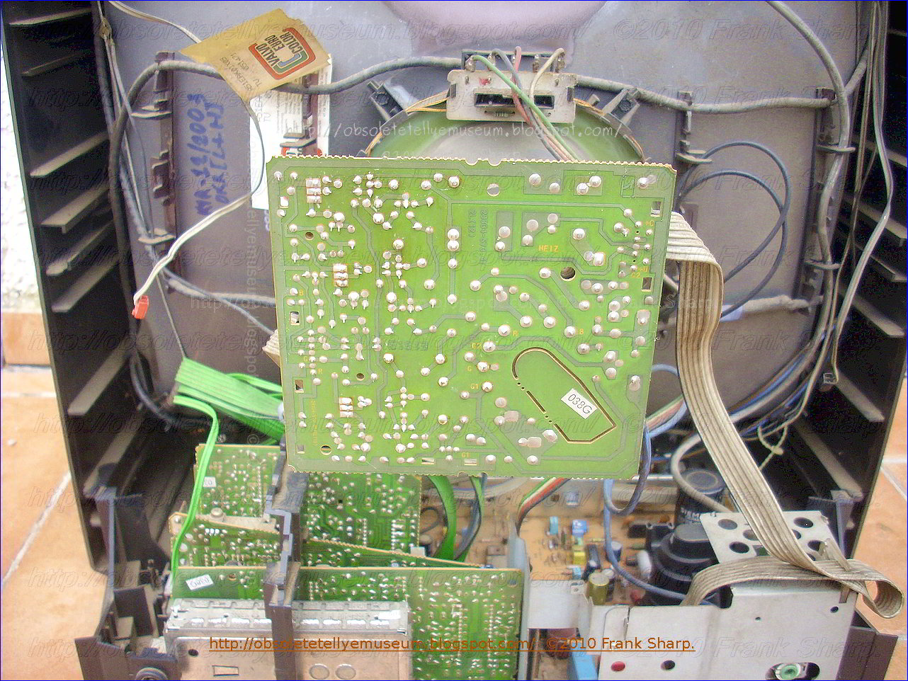
This chassis was reliable except for the EHT tripler which was failing very often.
The EHT tripler was causing sometimes big troubles.
GRUNDIG CHASSIS CHASSIS CUC3510 CUC3410 DESCRIPTION OF THE ZNT - LINE SUPPLY TRANSFORMER TECHNOLOGY, ONE TRANSFORMER FOR ALL FUNCTIONS :
Short Functional Description
The GRUNDIG line/power supply unit has two important features:
- the line/mains transformer (ZNT) with ferrite core.
This transformer is provided with windings for the power supply and line output stages:
- the supply frequency corresponds to the line frequency.
The ZNT is used for electrical isolation, horizontal deflection, and
generation of the operating voltage. The ZNT windings are tightly and
loosely coupled to ensure that the load capacity of the supplies is high
enough and that back effects on the line transformer winding N-M are
avoided.
Startup Circuit
The starting voltage for IC 655 is
obtained from the bridge rectifier D 621 via R 641. If the voltage on
pin 2, which is derived from the resistor network R 642, 643, and 644,
reaches a level of approximately 10 V, the IC 655 starts to drive T 661
via pin 3 (precondition: pin 18 >10V). The line/power supply circuit
starts to oscillate. Simultaneously, the current consumption drawn via
pin 2 rises and the winding E-D of the ZNT takes over the operating
voltage supply function (D 647, R 647, C 647).
Oscillator in IC TDA 3640
The
control pulses for the T 661 are generated by are generated by an
oscillator which operates on the threshold principle where C 653 is an
externally connected frequency-determining component (oscillator
retaining range 14-17 kHz approx.). The oscillator oscillates at a
free-running frequency until the reference pulses from the ZNT exceed 1
V, at pin 12. In full operating condition (ON) a voltage of about +5 V,
is applied to
pin 12.
Line Output Stage
The deflection transistor T 521 is activated in
stand-by mode. The cyclic line-frequency control of the deflection
transistor corresponds to the “ON“ operating mode. The power for the
horizontal sweep circuit is derived from the electromotive force of coil
M-N so that no additional operating voltage is necessary for T 521.
Voltage Stabilization In stand-by mode the pulse from winding E-D
(tightly coupled with winding A-B) is used as a reference for
stabilization. The controlled variable is +10.5 V on pin 2 TDA 3640. In
full operating condition, that is “ON", the voltage in the horizontal
sweep circuit (transformer winding M-N) must be stabilized to a constant
level. This is achieved by means of a reference pulse from winding C-D
which is tightly coupled with winding M-N. The resulting direct voltage
obtained via D 633 is proportional to the width of the picture or high
voltage and is applied to pin 10 and compared with the reference voltage
(about 3V) on pin 11. In this part of the circuit the +C voltage is
adjusted by means of R 637 to 196 V and 192 V for 25” receivers and 28” receivers, respectively.

Protective Circuits of TDA 3640
The protective circuits respond immediately if:
— the operating voltage on pin 2 is too low (<7 V):
— Ice of T 521 is too high (more negative than —1 V at pin 7);
— the power supply voltage is too high (voltage at pin 18 is 2.8 V higher than at pin 2);
— the power supply voltage is too low (voltage at pin 18 is 1.4 V lower than at pin 2):
— the high voltage is excessively high (line flyback pulses =6 V at pin 12);
— the crystal temperature is too high (>135° C).
Protective Circuits of TDA 8140
The protective circuits respond immediately if:
— the operating voltage at pin 2 is too low (<7 V);
— interference pulses (incorrect control pulses) occur during line flyback;
— the crystal temperature is too high (>160° C).
GRUNDIG SUPER COLOR M55-355A CTI CHASSIS CUC3510 : SYNCHRONIZED SWITCHED-MODE POWER SUPPLY UNIT WITH POWER LINE ISOLATED HORIZONTAL OUTPUT STAGE IN TELEVISION RECEIVER:


GRUNDIG CHASSIS CUC3400 - 3510: Standby mode operation of a horizontal output stage combined with a switched-mode power supply unit. STANDBY-BETRIEB BEI EINER MIT EINEM SCHALTNETZTEIL KOMBINIERTEN HORIZONTALENDSTUFENSCHALTUNG:
1. Swi
tched-mode power supply with a combined horizontal output stage
circuit in television receivers, in which, as a point of electrical
isolation between mains and chassis side, only a transformer (1) is
provided, the primary winding (n1 ) of which is tightly coupled to at
least one chassis-side secondary winding (n3 ) and one mains-side
secondary winding (n5 ) and is loosely coupled to further secondary
windings (n2 , n4 , n6 , n7 ) which, in turn, are tightly coupled to
each other, in which arrangement one of the secondary windings (n2 )
tightly coupled to each other is electrically connected to the
deflection transistor (4) of the horizontal output stage (14), and in
which a primary-side regulating circuit (2), which is synchronized by
flyback pulses in normal operation, controls a regulating switch which
is arranged in series with the primary winding (n1 ) of the transformer
(1), characterized in that - the deflection transistor (4), which is
periodically triggered in normal operation, of the horizontal output
stage (14) is kept continuously conductive by the driver circuit (13) in
standby mode of operation, - the amount of energy transferred from the
mains-side to the chassis side is corrected in accordance with the
determination of the supply voltage of the regulating circuit (2), which
is obtained via the mains-side secondary winding (n5 ) tightly coupled
to the primary winding (n1 ), during the standby mode of operation
during which no flyback pulses are supplied to the regulating circuit, -
and the energy needed in standby mode of operation on the chassis side
for the driver circuit (13) and other loads is transferred via the
chassis-side secondary winding (n3 ) tightly coupled to the primary
winding (n1 ).
1. Schaltnetzteil mit kombinierter Horizontalendstufenschaltung in Fernsehempf·angern, bei dem als galvanische Tren
nstelle zwischen Netz- und Chassisseite nur ein
Transformator vorgesehen ist, dessen Prim·arwicklung mit mindestens
einer weiteren Wicklung fest und den anderen Wicklungen, die fest
aneinandergekoppelt sind, lose gekoppelt ist, wobei eine der fest
miteinander verkoppelten Sekund·arwicklungen mit dem Ablenktransistor
der Horizontalendstufe elektrisch verbunden ist, d a d u r c h g e k e n
n z e i c h n e t , dass der Ablenktransistor (4) der
Horizontalendstufe und der Regelkreis (2), der von einer lose an die
Prim·arwicklung (n1) angekoppelten Sekund·arwicklung (n4) mit
R·uckschlagimpulsen versorgt wird, zur Steuerung des Standby-Betriebes
verwendet werden. 2. Schaltnetzteil nach Anspruch 1, d a d u r c h g e k e n n z e i c h n e t , dass der Ablenktransistor (4) der Horizontalendstufe zum Einschalten und/oder zum Wiedereinschalten des Normalbetriebes verwendet wird.
3. Schaltnetzteil nach Anspruch 1 oder 2, d a d u r c h g e k e n n z e i c h n e t , dass zum Einschalten des Standby-Betriebes der Ablenktransistor (4) leitend geschaltet, zum Aufrechterhalten des Standby-Betriebes leitend gehalten und zum Wiedereinschalten des Normalbetriebes gesperrt wird.
4. Schaltnetzteil nach einem oder mehreren der vorhergehenden Anspr·uche, d a d u r c h g e k e n n z e i c h n e t , dass der Regelkreis (2) bei einem Kurzschluss der Wicklung infolge einer sekund·arseitigen St·orung zur·uckgeregelt wird bzw. in den Standby-Betrieb umschaltet. EMI11.1

In einer zweiten, fest an die Prim·arwicklung n1 angekoppelten Wicklung n3 wird die Niedervoltspannung f·ur die Horizontalansteuerung, die einen internen Treiber enth·alt, und die Kleinsignalstufen erzeugt. Weiterhin sind Sekund·arwicklungen vorgesehen, die fest an n2 gekoppelt sind und die Spannungen f·ur die kGB-Endstufen, Heizung, usw. erzeugen.
·Uber die Trennstelle n /n des Transformators wird 12 w·ahrend des R·ucklaufintervalles des Ablenktransistors (4) eine Spannung a
uf die
Prim·arwicklung n1 ·ubertragen, die zur Ausschaltung des Regel schalters
verwendet wird. In der fest an die Wicklung n2 gekoppelten Wicklung n4
wird eine Spannung induziert, die zur Synchronisation und Steuerung des
Regelkreises 2 herangezogen wird. Der durch den Widerstand (6)
fliessende Strom kann als ·Uberlast-Referenzstrom zum Abschalten des
Regelschalters herangezogen werden.
Belastungs·anderungen werden in der fest an n2 gekoppelten Wicklung n4 erfasst und ·uber eine Beeinflussung der Stromflusszeit des Hauptstromkreises ausgeregelt.
Die deutsche Anmeldung P 32 10 908 enth·alt jedoch keinen Hinweis auf einen Standby-Betrieb.
Weiterhin ist aus der DE-PS 24 58 302 ein Sperrwandler-Netzteil f·ur einen Fernsehempf·anger mit Ultraschall-Fernbedienung bekannt, der als Betriebszustand u. a. einen Bereitschaftsbetrieb aufweist. Bei dieser Schaltung sind der Fernsehempf·anger und der Ultraschallempf·anger an denselben Trenntransformator sekund·arseitig angeschlossen. Die Umschaltung zwischen Normalbetrieb und Bereitschaftsbetrieb wird auf der Sekund·arseite des Trenntransformators vorgenommen.
Bei dieser Schaltung ist jedoch ein zus·atzlicher Transformator f·ur die Horizontalendstufe n·otig.
Die Aufgabe der Erfindung besteht darin, bei einem Schaltnetzteil mit kombinierter Horizontal-Endstufenschaltung der im Oberbegriff des Anspruchs 1 angegebenen Art auf besonders einfache Art und Weise den Standby-Betrieb zu erm·oglichen.
Diese Aufgabe wird durch das Kennzeichen des Patentanpsruchs 1 gel·ost. Besonders vorteilhafte Weiterbildungen der Erfindung sind in den Unteranspr·uchen gekennzeichnet.
Dic Vorteile der Erfindung liegen insbesondere darin, dass als galvanische Trennstelle nur ein Transformator f·ur die Erzeugung der Betriebsspannung, der Hochspannung, der Horizontalablenkung und der Heizspannung n·otig ist und aufgrund der gew·ahlten Wicklungsanordnung mit Hilfe des Horizontal-Ablenktransistors und der prim·arseitigen Regelschaltung auf besonders einfache Art und Weise eine Steuerung des Standby-Betriebes durchgef·uhrt werden kann.
Ein weiterer Vorteil besteht darin, dass im Falle einer sekund·arseitigen St·orung automatisch der Standby-Betrieb herbeigef·uhrt wird.
Die Erfindung wird nachfolgend unter Bezugnahme auf das aus der Figur 1 ersichtliche Ausf·uhrungsbeispiel n·aher erl·autert.
Die Schaltun
g wird ·uber die Netzspannung UN mit nachgeschalteter
Gleichrichterbr·ucke mit einer ungeregelten Gleichspannung versorgt und
ist ·uber nur einen Transformator 1 vom Netz getrennt, wobei der
Transformator die Stromversorgung f·ur das synchronisierte
Schaltnetzteil sowie die Impuls- bzw. Hochspannungserzeugung ·ubernimmt.
Wie durch die gestrichelte Linie zum Ausdruck kommt, ist die Netzseite
v·ollig von der Schaltungsseite galvanisch getrennt.In der Anlaufphase wird ·uber eine Startschaltung 7, die im einfachsten Fall aus einem hochohmigen Widerstand besteht, der Kondensator 11 aufgeladen. In dieser Phase gibt die Regelschaltung 2 keine Impulse an die Basis des Regelschalters 3 ab. Erst wenn die Spannung am Punkt A einen vorgegebenen Wert (z. B.
10 V) erreicht hat, wird ·uber eine regelschaltungsinterne Stabilisierungsschaltung die gesamte Schaltung in Betrieb genommen. Die Regelschaltung 2 liefert Impulse an die Basis des Regelschalters 3, tastet also den Regelschalter 3 auf. ueber den Regelschalter 3 fliesst somit ein pulsierender Strom in die Prim·arwicklung n1 des Transformators.
Die Wicklungen nl, n3 und n5 sind fest miteinander verkoppelt. Die Wicklungen n2, n4, n6 und n7 sind untereinander fest, aber lose an die vorgenannten Wicklungen nl, n3 und n5 gekoppelt. Ein Beispiel daf·ur, wie die genannten Kopplungsverh·altnisse erreicht werden k·onnen, zeigt die Figur 2.
Die Wicklu
ng n5 liefert ·uber eine Diode 10 einen gegen·uber der
Anlaufphase h·oheren Strom an den Kondensator 11, so dass in der
weiteren Folge die Versorgung der Regelschaltung 2 sichergestellt ist.Durch die zweite, fest an n1 und lose an n2 angekoppelte Sekund·arwicklung n3 wird die Niedervoltspannung f·ur die Kleinsignalstufen und die NF-Stufe und den Horizontaloszillator bzw. die Treiberschaltung 13 der Horizontalendstufe 14 gewonnen, und damit die Ansteuerung des Ablenktransistors 4 sichergestellt. In die lose an n1 gekoppelte Sekund·arwicklung wird n2 In die lose an n1 gekoppelte Sekund·arwickl£ung n2 wird eine Spannung induziert, die nach Gleichrichtung mittels einer Diode 8 an den Kondensator 9 die ben·otigte Betriebsspannung f·ur den Ablenkkreis liefert und somit den Anlauf der Horizontalendstufe herbeif·uhrt.
·Uber die Trennstelle n 1/n2 wird ferner die an der Ablenkwicklung 15 stehende Spannung w·ahrend des K·ucklaufintervalls der Ablenkschaltung invertiert auf die Prim·arwicklung n1 betragen, um den Strom im Hauptstromweg w·ahrend der R·ucklaufzeit bei der Schaltung des Regelschalters 3 und damit die Abschaltverluste zu vermindern. Dieser Vorgang ist ausf·uhrlich beispielsweise in der DE-OS 28 35 946 dargestellt.
Aus einer fest an die Wicklung n2 und lose an n1 angekoppelten Wicklung n4 des Transformators wird eine R·ucklauf spannung gewonnen, die abh·angig von der Belastung der Wicklung n2 ist.
Strahlstrom·anderungen in der Hochspannungserzeugung ·uber die Wicklung n6 und der Hochspannungskaskade 12 (bzw. Split) werden ·uber die fest an n6 gekoppelte Wicklung n2 bzw. die fest an n2 ge
koppelte Wicklung n4 an die
Regelschaltung 2 weitergegeben, die die Stromflusszeit im
Hauptstromkreis bzw. den Regelschalter 3 beeinflusst. Somit werden ·uber
die Regelschaltung 2 Belastungsschwankungen ausgeregelt.Hingegen werden Belastungs·anderungen in der Wicklung n3, wie sie beispielsweise durch NF-Last·anderungen gegeben sind, fast nicht nachgeregelt, da die Wicklung n3 nur lose mit den Wicklungen n2 und n4 verkoppelt ist. Deshalb ist die Zeilenablenkschaltung weitgehend unabh·angig von Last·anderungen in der Sekund·arwicklung n3.
Die Netzspannungsnachregelung f·ur die Spannungen, die aus der Wicklung n3 gewonnen werden, erfolgt indirekt ·uber die Regelimpulse der Wicklung n4 So w·urde sich beispielsweise bei Netzunterspannung die R·ucklauf spannung ohne Nachregelung verringern.
Durch die Impulse der Wicklung n4 wird jedoch ·uber die Regelschaltung 2 die Leitzeit des Regelschalters 3 verl·angert. Damit wird mehr Energie von der Prim·arauf die Sekund·arseite ·ubertragen und demzufolge Netzspannungs·anderungen ausgeglichen.
Bei der Umschaltung vom Normalbetrieb in den Standby- Betrieb schaltet der Regelkreis 2 die Spannung ¢am Punkt A auf den vorgegebenen Wert von z. B. 10 V.
Diese Standby-Umschaltung steht in Verbindung mit einer Verk·urzung der Leitzeit des Regel schalters 3, die wie folgt ausgel·ost wird: ·Uber die Wicklung n3 bzw. eine Treiberschaltung 13 der Horizontalansteuerstufe wird die Basis des Ablenk transistors 4 so gesteuert, dass der Ablenktransistor st·andig leitet. Demzufolge kann sich im Kondensator 9 und damit auch in der Sekund·arwicklung n2 keine Spannung aufbauen. Da die Wicklung n6 f·ur die Hoch spannungs erzeugung, die Wicklung n7 f·ur die Erzeugung einer Heizspannung und sonstige Impulsspannungen sowie die Wicklung n4 f·ur die Synchronisation und Steuerung der Regelschaltung 2 fest mit der Wicklung n2 verkoppelt sind, k·onnen weder Hochspannung noch Heizung noch sonstige Impuls spannungen entstehen.
Damit sind s·amtliche im Standby-Betrieb nicht ben·otigten Spannungen abgeschaltet, ziehen also keine Leistung aus dem Netz. Ausserdem schaltet wegen des Wegfalls der R·ucklauf spannungen an n4 die Regelschaltung im beschriebenen Sinne den Regel schalter 3 auf Standby-Betrieb um.
Dagegen ist die im Standby-Betrieb n·otige Versorgung der Sekund·arseite mit Niedervoltspannung weiterhin gew·ahrleistet, da die Wicklung n3, ·uber die diese Versorgung erfolgt, fest mit der Prim·arwicklung n1 und nur lose mit der Sekund·arwicklung n2 verkoppelt ist. Die Nachregelung der Niedervoltspannung kann - falls n·otig - mit Hilfe der Spannung erfolgen, die in die ebenfalls fest an n1 gekoppelte Wicklung n5 induziert wird, die ansonsten nur die Energie f·ur die Versorgung der Regelschaltung liefert.
 Der ·Ubergang vom Standby-Betrieb auf den
Normalbetrieb geschieht durch die Sperrung des Ablenktransistors 4 und
dessen weitere periodische Ansteuerung. Die an der Wicklung n2
entstehende Spannung wird in der fest an n2 gekoppelten Wicklung n4
induziert. Diese R·uckschlagimpulse gelangen an den Triggereingang der
Regelschaltung 2. Diese f·uhrt einen internen Spannungsvergleich durch
und f·uhrt die Schaltung wieder in den geregelten Normalzustand ·uber.
Der ·Ubergang vom Standby-Betrieb auf den
Normalbetrieb geschieht durch die Sperrung des Ablenktransistors 4 und
dessen weitere periodische Ansteuerung. Die an der Wicklung n2
entstehende Spannung wird in der fest an n2 gekoppelten Wicklung n4
induziert. Diese R·uckschlagimpulse gelangen an den Triggereingang der
Regelschaltung 2. Diese f·uhrt einen internen Spannungsvergleich durch
und f·uhrt die Schaltung wieder in den geregelten Normalzustand ·uber.Die dargestellte Schaltung erm·oglicht es somit, den Ablenktransistor 4 der Horizontalendstufenschaltung in besonders einfacher Weise f·ur die Steuerung des Standby-Betriebes zu verwenden.
Ein besonderer Vorteil der erfindungsgem·assen Schaltung liegt darin, dass im Falle einer sekund·arseitigen St·orung, z. B. einem Kurzschluss der Diode oder des Kondensators 16, die Schaltung automatisch in den Standby-Betrieb ·ubergef·uhrt wird. Denn im Falle eines Kurzschlusses der Diode 8 oder des Kondensators 16 kann sich an n2 keine Spannung aufbauen. Dies gilt ebenso f·ur die Wicklung n4, die fest an n2 gekoppelt ist und die R·uckschlagimpulse an den Triggereingang der Regelschaltung 2 liefert. Auch an der Wicklung n6 f·ur die Hochspannungserzeugung und der Wicklung n7 f·ur die Erzeugung einer Heizspannung, die beide ebenfalls fest an n2 gekoppelt sind, kann sich keine Spannung aufbauen.
GRUNDIG SUPER COLOR M55-355A CTI CHASSIS CUC3510 Regulated power supply device for a line sweep circuit in a television receiver:

1. A regulated power supply device, in particular for a line sweep circuit in a television receiver, whose output stage (30) contains a first electronic switch of the bidirectional type (36, 35), controlled periodically so as to be closed during the forward sweep and open during the fly-back, connected in parallel with a first series assembly containing line deviation coils (31) and a first capacitor (32), called the forward capacitor, which feeds these coils (31) during the closing of the first switch (36, 35), with a second capacitor (34), called the return capacitor, which forms a parallel resonant circuit with the inductance in particular of the coils (31) during the opening of the first switch (36, 35) and with a second series assembly containing a first winding (22) of a transformer (20), called the line transformer, and a third capacitor (33), called the power supply capacitor, which feeds the first winding (22) with D.C. voltage while the first switch (36, 35) is closed, the power supply device containing a chopper circuit (10) connected between the terminals (6, 7) of a D.C. power supply voltage source (5) and containing an inductor, called the chopper inductor, (16) and a second electronic switch (15), which is controlled, mounted in series, this second switch (15) containing a chopper transistor (11) controlled on its base by means of a recurring control signal, which is produced by means of the line return pulses picked up on a secondary winding (25) of the line transformer (20), in order to be alternately conducting and cut off during each line period, this chopper inductor (16) containing a second winding (21), called the power supply winding, of this transformer (20), which is intended for the transfer of energy between the chopper circuit (10) and the line sweep output stage (30), and being characterized by the fact that, the second switch (15) being also of the bidirectional type and containing, apart from the chopper transistor (11), which is operating in the saturated and cut off mode, a diode (12) mounted in parallel and in opposition with this transistor, the chopper circuit (10) contains also a fourth capacitor (13), called the turning capacitor, which forms a resonant circuit with the chopper inductor (16) during the opening periods of the second switch (15) which works with a constant cyclic ratio, the periods being obtained by means of a control signal which causes the cutting off of the chopper transistor (11) and their lengths being constant and greater than a half period of resonance of this resonant circuit (13, 16) whose length may reach about a half of a line period, and by the fact that the regulation of the energy exchanged between the chopper circuit (10) and the output stage (30) is obtained by the variation of the delay between the respective opening instants of the first
(36, 35) and second (15) switches.
2. A power supply device as in claim 1, characterized by the fact that the transistor (11) in the second switch (15) is controlled by means of a regulation circuit (40) fed by an auxiliary winding (25) of the transformer (20) which supplies it with a signal one of whose peak amplitudes is proportional to the voltage at the terminals of the power supply capacitor (33) in the output stage (30), which is recharged by means of the chopper circuit (10), and whose peak to peak amplitude is proportional to a very high voltage supplied by another winding (23) of transformer (20), the regulation circuit (40) causing the delay in the instant of cut off of transistor (11) to vary with respect to the leading edge of the line return pulse produced by the opening of the first switch (36, 35).
3. A power supply device as in claim 2, characterized by the fact that the regulation by the phase shift between the respective cut off instants is obtained as a function either of the peak to peak amplitude or of the peak amplitude during the fly back or forward sweep of the signal at the terminals of one of the windings (21 or 25) of line transformer (20) by comparing this amplitude to a reference voltage and by controlling the delay as a function of the difference between the voltage corresponding to one of these amplitudes and the reference voltage, in order to stabilize either the sweep amplitude or the power supply voltage obtained by rectifying the line return pulse.

4. A power supply device as in claim 2, characterized by the fact that the regulation circuit (40) contains an unstable multivibrator (48) whose output is coupled to the base of chopper transistor (11) by means of a control stage (50) and which operates independantly on starting up, a circuit generating a variable delay which contains a phase shift stage (46) triggered by the line return pulses and supplying to the multivibrator (48) triggering pulses which are delayed with respect to the leading edges of the line return pulses, which cause the cutting off of chopper transistor (11), and a regulator stage (47), which supplies the phase shift stage (46) with a regulation signal that makes it possible to vary the delay between the respective leading edges of the line return pulses and the triggering pulses as a function of one of the peak amplitudes or of the peak to peak amplitude of the signal supplied by the auxiliary winding (25) of the transformer (20).
5. A power supply device as in claim 4, of the type in which the power supply capacitor (33) feeds a D.C. voltage to the whole line sweep circuit, characterized by the fact that the regulation circuit (40) is fed by means of an independant power supply circuit (51) which enables the chopper circuit (10) to be started up by the independant operation of the unstable multivibrator (48) in order to start up the power supply of the line sweep circuit with the chopper voltage induced in the first winding (22) of the transformer (20) and rectified by the diode (35) which is part of the first bidirectional switch (36, 35) which charges the power supply capacitor (33).
6. A power supply device as in one of claims 4 and 5, characterized by the fact that the phase shift stage (46) contains a delay generator which supplies a voltage, in the shape of recurrent saw teeth (460, 463) which are triggered by the leading edges of the line return pulses, to an analog voltage comparator stage (469, 4600, 4601), which supplies at its output negative pulses to the base of the transistor (483) in multivibrator (48) whose cutting off controls the cut off of chopper transistor (11) at instants at which the instantaneous saw tooth amplitude exceeds a fixed threshold voltage (VZ 4601), and by the fact that the regulator stage (47) contains an assembly (470, 471) rectifying the signal supplied by the auxiliary winding (25) which feeds a signal generator (476, 475) supplying a signal which modifies, from a predetermined threshold, the saw tooth slope as a function of one of the peak amplitudes or peak to peak amplitudes of this signal (v25).
7. A power supply device as in claim 6, of the type in which the free running operating frequency of the unstable multivibrator (48) is less than the line frequency, characterized by the fact that the unstable multivibrator (48) is controlled solely by the negative pulses coming from the comparator stage (469), which are applied to one (483) of the transistors in the multivibrator (48), whose cut off controls that of chopper transistor (11).

8. A power supply device as in one of claims 4 to 6, of the type in which the free running operating frequency of the unstable multivibrator (48) is greater than the line frequency in order to limit the peak voltage (V19max) on the collector of the chopper transistor (11), characterized by the fact that the transistor (480) in the multivibrator (48), whose state is complementary to that of the chopper transistor (11), is fed on its base through a diode (4803) by a synchronizing stage (49), which supplies negative pulses whose amplitude is equal to a predetermined fraction of that of the line return pulses, in order to lengthen the cut off state of this transistor (480) until the sum of these lengths is equal to the line period.
Description:
The present invention concerns a regulated power supply device, in particular for a line sweep circuit in a television receiver, which can also provide D.C. supplies to other circuits in this receiver by splitting up a D.C. supply voltage which is usually obtained by the rectification and filtering of the A.C. mains voltage by means of a chopper.
Known chopper converters of this type contain, generally connected in series between the output terminals of a D.C. power supply source (filtered rectifier), an electronic switch such as a switching transistor operating in the saturated and cut off mode and an inductor which includes the primary winding of a transformer in which at least one secondary winding supplies the A.C. energy obtained by the chopping, which is then rectified to provide the D.C. supply voltages with a ground insulated from the mains. In most of the known chopper power supplies, one can vary the output voltages by action on the cyclic ratio, i.e. the length of the saturated (closed) state of the switch, for example, by controlling periodically the transistor-chopper by means of a monostable flip-flop of variable length as a function of a voltage which may be picked up at the output of a rectifier fed by a secondary winding of the transformer so as to form a regulation loop.
Chopper power supplies have frequently been used in television receivers to eliminate the bulky and heavy mains supply transformer and make possible a regulation of the D.C. power supply voltage for this receiver. They have often been combined in particular at the output stage of the horizontal sweep circuit which supplies them with a pulse signal at the line frequency that can be used to control the chopping. Various combinations of sweep circuits and chopper power supplies have described, for example, in the French patents or patent applications with publication Nos. 2.040.217, 2.060.495, 2.167.549, 2.232.147 or 2.269.257, in which the regulation is also done by means of the variation in the cyclic ratio of the saturated and cut off states of the chopper transistor which, in some cases, is also used as the active element of the (final) output stage of the line sweep circuit or of the feeder stage which controls this circuit.

Chopper power supplies of the so called "pump" type in which the chopper transistor feeds one of the windings of the line transformer during the line return periods and in which the regulation is done by means of the variation of the internal resistance of this transistor or of a "ballast" transistor in series with this transistor are known, for example, from the French patents with publication Nos. 2.014.820, 2.025.365 or 2.116.335. A circuit of the "pump" type whose chopper transistor has a winding of the line transformer in its collector circuit and in which the sweep circuit is electrically insulated from the mains has been described in the article by Peruth and Schrenk in the German periodical, SIEMENS BAUTEILE REPORT Vol. 12 (1974), No. 4, pages 96-98. Its structure corresponds to the contents of the introduction to claim 1. In circuits of the "pump" type, the chopper transistor or the "ballast" transistor in series with it dissipates an amount of energy which is not negligable.
In the chopper device supplying power to the output stage of the line sweep circuit with which it is combined in accordance with the invention, one no longer uses regulation by variation of the internal resistance or of the length of the saturated state of the chopper transistor (or by variation of the cyclic ratio of the chopping with a constant periodicity) but one does the regulating by variation of the relative phase between the signals of the same frequency which are supplied respectively by the chopper circuit with a constant cyclic ratio and by the output stage of the line sweep, each of which is connected to one of the windings of a transformer called the line transformer through which the transfer of energy between the chopper circuit and the sweep output stage takes place as well as in the direction of the other secondary windings of the line tranformer such as the very high tension (V.H.T.) winding.
In accordance with the invention, a regulated power supply device, in particular for a line sweep circuit of a television receiver which contains an output stage fitted with a line transformer in which a first winding is connected in series with a s
upply
capacitor, is connected in parallel with a first bidirectional switch
controlled at the line frequency, the power supply device containing a
chopper circuit with, connected in series between the terminals of a
source of a D.C. power supply voltage, an inductor and a second
electronic switch, which can also be controlled at the line frequency.
The inductor in this circuit contains a second winding of the
transformer which is intended for the transfer of energy between the
chopper circuit and the output stage. This power supply device is in
particular characterized by the fact that the second switch, which is
also bidirectional and mounted in parallel with a tuning capacitor, is
so controlled as to be alternately open and closed during each line
period with a constant cyclic ratio and by the fact that the regulation
of the power supplied and hence of the voltage at the terminals of the
supply capacitor is done by variation of the phase delay between the
respective opening instants of the first and second switch as a function
of the peak amplitude of the line return pulse for example.
In accordance with a preferred way of making the invention, a power supply device in accordance with the preceding paragraph, in which the s
econd
bidirectional switch, which contains a switching transistor, is
controlled on its base by a regulation circuit in which one input is fed
by an auxiliary secondary winding of the line transformer supplying
line return pulses, is remarkable in particular for the fact that the
regulation circuit contains an unstable multivibrator controlling the
base of the chopper transistor and operating independantly on starting
up, a circuit generating a variable delay containing a phase shift
stage, which is triggered by the line return pulses and supplies the
multivibrator with triggering pulses that are delayed with respect to
the leading edges of the line return pulses, which cause the cut off of
the chopper transistor, and a regulator stage fed with the line return
pulses and supplying to the phase shift stage a regulation signal which
enables the delay in the triggering pulses to be varied with respect to
the line return pulses as a function of one of the peak amplitudes or of
the peak to peak amplitude of the line return pulses.The invention will be better understood and others of its characteristics and advantages will appear from the description which follows, which is given as an example, and the drawings attached, which refer to it. Among them:
FIG. 1 represents part of a theoretical schematic diagram of a chopper power supply device combined with the output stage of the line sweep circuit in accordance with the invention;
FIGS.
2a-2f and 3a-3f are diagrams of the voltage wave forms and/or current
wave forms at various points in the circuit of FIG. 1 to explain the
operation of this circuit;FIG. 4 represents part of a synoptic schematic diagram of a simple production model (without a starter device) of regulation circuit 40 in FIG. 1;
FIG. 5 represents a block diagram of a preferred production model of regulation circuit 40 in FIG. 1 in accordance with the invention;
 FIG.
6 represents a theoretical schematic diagram of the whole of the
preferred production model of the regulation circuit in FIG. 5;
FIG.
6 represents a theoretical schematic diagram of the whole of the
preferred production model of the regulation circuit in FIG. 5;FIGS. 7a and 7b represent voltage wave forms illustrating the slaving of the frequency of the unstable multivibrator 48 to that of the line oscillator; and
FIGS. 8a-8c represent voltage wave forms illustrating the operation of the regulation by the variation in phase shift.
In FIG. 1 is shown schematically a chopper power supply device of line sweep output stage 30 in accordance with the invention which is electrically insulated from the A.C. mains which feed rectifier 5 whose output voltage is chopped. This power supply device has two terminals 1, 2 which are connected respectively to the two poles of the A.C. distribution mains (220 V, 50 Hz) and feed rectifier diode 3 and filter capacitor 4, whose capacity is high, which are connected in series and form together a rectifier assembly or a source of D.C. voltage 5. The output of rectifier assembly 5 formed by the two terminals 6 and 7 (plates) of the (electro-chemical) capacitor 4 is intended to supply a D.C. power supply voltage V A of the order of 300 V to chopper circuit 10. This chopper circuit 10 contains a controlled, bidirectional electronic switch 15, which consists of a switching transistor 11 of the NPN type connected with its emitter common and a junction semiconductor diode 12, which are connected in parallel in such a way as to conduct respectively in opposite directions (anti-parallel), and an inductor 16 consisting of a choke 14 and a winding 21 of a transformer 20, called a line transformer, connected in series. This winding 21 of line transformer 20 whose primary winding is normally connected in parallel with the coils of the horiziontal deviation circuit in the circuit of line sweep output stage 30 to the supply, through secondary windings, supply voltages in particular to the cathode ray tube will be called in what follows the supply voltage winding, because the transfer of energy between chopper circuit 10 and output stage 30 will be done through it. Switch 15 is mounted in parallel with a capacitor 13 and it is connected in series with inductor 16 (choke 14 and power supply winding 21 in series) between the out
put
terminals 6 and 7 of D.C. voltage source 5. This capacitor 13 forms,
because of its low capacity with respect to that of filter capacitor 4,
with inductor 16 a parallel, resonant (oscillatory) circuit when
electronic switch 15 is opened by the cutting off of switching
transistor 11 by means of a control signal applied to its base.Switching transistor 11 is here connected by its collector to one of the terminals of inductor 16, whose other terminal is connected to positive terminal 6 of source 5 which supplies D.C. power supply voltage V A , by its emitter to negative terminal 7 of source 5, which forms a ground, called the primary or hot ground, 8, which is connected to the A.C. mains but is insulated from that 39 of the television set. The base of transistor 11 is controlled by means of rectangular signals supplied by a regulation circuit 40, which is described further on, in such a way as to be alternately saturated and cut off. Regulation circuit 40 is, for example, fed by a secondary winding 25 of transformer 20, that supplies signals whose peak to peak amplitude is proportional to the peak amplitude of the line return pulse. This peak amplitude is a function of the energy transfer from chopper circuit 10 to the line sweep output stage 30 which is connected to another winding 22 of transformer 20.
One may note here that chopper circuit 10 resembles a classical, transistorized, line sweep output stage and that switching transistor 11 has been chosen to withstand high collector-emitter voltages (of the order of 1500 V), and that diode 12 has to withstand the same inverse voltage while switch 15 is open. One may also note that the inductance of choke 14 may be formed partly or wholly by the leakage inductance of power supply winding 21 in transformer 20.
The line sweep output stage 30, which is arranged in classic
al fashion, contains horizontal
deviation coils 31 mounted in parallel and connected by one of their
terminals to a first capacitor 32, called the "forward" or "S effect"
capacitor, which feeds them during the forward sweep. The series
mounting of coils 31 and forward capacitor 32 is connected in parallel,
on the one hand, to a second controlled bidirectional switch containing a
second switching transistor 36 and a second diode 35, called a "shunt"
or "parallel" recuperation diode, which are connected in parallel to
conduct in opposite directions, closed (conductor) during the forward
sweep and open (cut off) during the return sweep, and, on the other
hand, to a second capacitor 34, called the "return" capacitor, which
forms, while the second switch is open, a parallel resonant circuit with
the inductance of deviation coils 31. The common point of the collector
of second transistor 36, of the NPN type, of the cathode of second
diode 35 and return 34 and forward 32 capacitors is connected to one of
the terminals 220 of winding 22 of transformer 20, which normally forms
the primary winding of this transformer. The other terminal 221 of
winding 22 is connected to one of the terminals of a third capacitor 33
of high capacity, whose other terminal is connected to the common point
of deviation coils 31, return capacitor 34, the anode of second diode 35
and the emitter of second transistor 36, which is also connected to the
ground 39 of the chassis of the television receiver, called the "cold"
ground, because it is insulated from the A.C. power supply mains. It is
at the terminals of this third capacitor 33 that one obtains the D.C.
voltage feeding this stage, whose value determines, on the one hand, the
peak to peak amplitude of the line sweep current of sawtooth form and,
on the other hand, the amplitude of the line return voltage pulse which,
when rectified after being transformed, supplies the very high voltage
that polarizes the anode of the cathode ray tube (not shown here). The
second transistor 36, also a switching transistor, is controlled by
rectangular shaped signals supplied to input terminals 37 and 38 of
stage 30, which are respectively connected to its base and its emitter,
by a feed stage (not shown and called a "driver" in anglo-american
literature) so that it is alternately cut off, during the sweep return,
and saturated, during the second part of the forward sweep.In classical transistor line sweep circuits, a D.C. voltage source generally feeds either terminal 221 of winding 22 directly or an intermediate connection to this winding through a diode (see French Pat. Nos. 1.298.087 dated Aug. 11, 1961, 1.316.732 dated Feb. 15, 1962 or 1.361.201 dated June 27, 1963) which isolates the primary winding of the line transformer from the D.C. voltage source during the line return interval.
In
the circuit of FIG. 1, it is the A.C. electrical energy transmitted by
chopper circuit 10 through windings 21 and 22 of transformer 20 which
charges capacitor 33 so that it supplies a regulated supply voltage to
output stage 30. During the line sweep forward periods, when the second
bidirectional switch 35, 36 of sweep output stage 30 is closed
(conductor), the terminals of winding 22 of transformer 20 are directly
connected to those of capacitor 33 which will then receive the energy
supplied of by chopper circuit 10.In FIG. 1, line transformer 20 also has a very high voltage winding 23, one terminal 230 of which may be connected to the ground 39 (or to terminal 220 of winding 22) and whose other terminal 231 is connected to the input of the very high voltage rectifier assembly or voltage multiplier (not shown) in classical fashion, and an auxiliary winding 24 which may be used to feed either a low voltage rectifier assembly or a load regulator assembly or the filament of the cathode ray tube (not shown). These secondary windings 23, 24 will receive their energy mainly from output stage 30 of the line sweep circuit through winding 22 of transformer 20, i.e. the line return pulses, the coupling between the windings will hence be as close as possible.
The operation of the power supply device in FIG. 1 will be explained below with that of output stage 30 of the line sweep circuit, with reference to FIGS. 2 and 3 of the drawing attached, representing diagrams of the voltage wave forms and/or current wave forms at various points in the schematic diagram of FIG. 1.
In
FIGS. 2 and 3, diagram (A) represents the saw tooth wave form of the
sweep current i 31 (t) in the coils 31 of the horizontal deviation
circuit. Diagram (B) represents the wave form of the voltage v 220 (t)
on terminal 220 of winding 22, which is also that at the terminals of
the second switch 35, 36. Diagram (C) is the wave form of the voltage v
21 (t) at the terminals of power supply winding 21 when its leakage
inductance is negligable. It is obtained by the transforming of the A.C.
component of voltage v 220 (t). Diagram (D) represents the wave form of
the voltage v 19 (t) at the terminals of first switch 15 in chopper
circuit 10, i.e. between the junction 19 of this chopper circuit with
inductor 16 and primary ground 8, and diagram (E) represents as a dotted
line the current i 16 (t) in inductor 16 when output stage 30 is not
controlled and as a full line the current i 21 (t) resulting from the
superimposition in winding 21 to current i 16 (t) on that induced by
winding 22 when output stage 30 is working. Conversely, the current in
winding 22 of transformer 20 results from the superimposition of the
current induced by winding 21 on the current produced by the closing of
the second switch 35, 36, which is analogous to i 31 (t) in diagram (A).The wave forms of diagrams (D) and (E) in FIGS. 2 and 3 are out of phase respectively, one with respect to another, by a quarter of a line period T H /4 to allow the illustration of the regulation by the variation in the relative phase of the voltage v 21 and current i 21 waves in power supply winding 21.
The diagrams (F) represent the instantaneous energy E i transmitted by chopper circuit 10 to the output stage 30, which is equal to the product of the wave forms of current i 21 (t) and voltage v 21 (t) in winding 21, i.e. E i =-v 21 i 21 , for two different phase deviations between the voltage v 21 (t) and current i 21 (t) waves in power supply winding 21, which correspond respectively to a zero energy transfer in FIG. 2 and a maximum energy transfer in FIG. 3.
The operation of the line sweep output stage 30 is classical once the power supply capacitor 33 and forward capacitor 32 are charged to a D.C. voltage V 221 by means of a certain number of chopping cycles, which are independant on starting up, during which the negative half-cycles of the chopped voltage wave are rectified by recuperation diode 35.
During the forward sweep intervals t A , when the switch 35, 36 is closed from instant t 1 to instant t 3 , the current i 31 (see A) in the deviator varies roughly linearly between its negative peak values (at t 1 ) and positive ones (at t 3 ) with a passage through zero at instant t 2 , when current i 31 passes from diode 35 to transistor 36, which has previously been polarized to conduct. This corresponds to a roughly zero voltage v 220 (see B) at the terminals of switch 35, 36.
The line return interval t R is started by the cutting off of transistor 36 at instant t 3 , and the inductance of deviator 31 then acts as a parallel resonant circuit with the return capacitor 34 by causing the voltage v 220 (t) to pass through a positive half-sinusoid and reach its peak value at the instant t 4 (or t=0), called the line return pulse, and the current i 31 (t) to pass through a half-cosinusoid between the positi
ve
and negative peak values cited, with a passage through zero at the
instant t 4 (or t=0). The mean value of the voltage wave form v 220 (t)
at terminal 220 is equal to the D.C. power supply voltage V 221 at the
terminals of power supply capacitor 33 and forward or S effect capacitor
32.The respective peak to peak amplitudes of current i 31 (t) (hence the width of the screen sweep beam excursion) and of voltage v 220 (t) (hence the very high voltage) depend on the value of the D.C. voltage V 221 which feeds the horizontal sweep output stage and which, in most of the chopper power supplies of preceding techniques, is regulated and stabilized by modulating the length of the saturated state (the cyclic ratio) of chopper transistor 11 as a function of the amplitude of the line return pulse picked up on an auxiliary winding of line transformer 20 (hence of the voltage at the terminals of capacitor 33) and later of the rectified and filtered voltage in the network.
In accordance with the invention, the length t s of the saturated state of chopper transistor 11 and of the conducting state of diode 12 and, as a result, the ratio of this length to that of the complete cycle (line period T H ) or to that t B of the cut off state is constant and so chosen as to make the peak amplitude of voltage pulse v 19 , which is applied to the collector of transistor 11 during the cut off interval t B , considerably less than its collector-emitter D.C. breakdown voltage in the cut off state (V CEX ) which may exceed 1500 Volts. Thus, for a rectified voltage of 300 V, it is possible to limit the collector voltage V 19 to about 900 Volts by choosing a ratio t b /T H of about 0.5.
As a result, chopper circuit 10 must operate at the line frequency with conduction lengths t S (closed) and cut off lengths t B (open) of switch 15 preferably roughly equal (to a line half-period T H /2) and the regulation of the energy supplied to output stage 30 is done by causing the respective phases of the line return pulse v 220 (t) and the current i 21 (t) flowing through the power supply winding 21 of transformer 20 to vary as will be shown further on.
The operation of chopper circuit 10 (fed with D.C. voltage V A ) is in fact analogous to that of output stage 30, except as far as the form factor is concerned. This is determined mainly by the respective values of the inductance 16 (of choke 14 and the leakage inductance of winding 21 of transformer 20 connected in series) and of the capacity of tuning capacitor 13. The values L 16 and C 13 are chosen to obtain a half-period of oscillation slightly less than a line half-period, i.e.: ##EQU1## because the oscillation of the resonant circuit L 16 , C 13 occurs on one side and on the other of the D.C. voltage V A so that the cut off period of chopper switch 15 is greater than this half-period T D /2.
This operation of circuit 10 will first be explained with reference to diagrams D and E in FIG. 2. When, at the instant t=0, transistor 11 becomes saturated by a preliminary positive polarization of its base-emitter junction, it connects terminal 19 to ground 8 so that a current i 16 (t) (dotted on diagram E), which is increasing linearly, ##EQU2## passes through inductor 16 coming from positive terminal 6 of power supply 5.
When transistor 11 receives from regulation circuit 40 a cut off voltage at an instant preceding instant t 6 of the storage time of minority charge carries, switch 15 opens and the current stored in inductor 16, i 16 (t 6 )=V A t 6 /L=V A T H /4L, will flow through tuning capacitor 13 in oscillatory fashion, i.e. cosinusoidally, decreasing to a zero value, while voltage V 19 at junction 19 of inductor 16 and capacitor 13 will increase sinusoidally to a maximum value, these two values coinciding in time. Then, capacitor 13 discharges through inductor 16 also in oscillatory fashion until, at instant t 7 , voltage v 19 reaches a zero value, which corresponds to a minimum value, i.e. maximum negative, of current i 16 (t) whose absolute value is slightly less than the maximum positive value i 16 (t 6 ). The difference between the absolute peak values i 16 (t 6 ) and i 16 (t 7 ) is explained, on the one hand, by the ohmic losses in circuit 10 and, on the other, by the transfer of energy between this circuit and, in particular, output stage 30.
When oscillatory voltage v 19 (t)
has exceeded the zero value slightly in the negative direction, diode
12 starts to conduct so as to connect terminal 19 to ground and produce
in inductor 16 a current i 16 (t), which increases linearly from its
maximum negative value i 16 (t 7 ) towards a zero value where transistor
11, which has already been polarized so as to be saturated, picks it up
so that it reaches, at instant t 8 , its maximum positive value of
instant t 6 again.It is to be noted here that the mean value of the wave form of voltage v 19 at terminal 19 is equal to the D.C. power supply voltage V A between terminals 6 and 7 of filter capacitor 4 in rectifier assembly 5.
If one wishes to obtain an adequate energy transfer between chopper circuit 10 and line sweep output stage 30, it is advantageous to choose the value of inductor 16 in series with power supply winding 21, i.e. the sum of the leakage inductance of this winding and that of series choke 14, so that it is, for example, greater than or equal to three times the inductance L 31 of the horizontal deviation coils 31, multipled by the square of the transformation ratio between windings 22 and 21, i.e. L 16 ≥3l 31 (n 11 /n 21 ) 2 , and the value of this transformation ratio n 22 /n 21 so as to obtain at the terminals of winding 21, during the forward sweep and the closing of switch 15, an induced voltage v 21 (t) whose amplitude is between 100 and 150 Volts, i.e. between a third and a half the power supply voltage V A at terminals 6, 7 of filter capacitor 4.
As the D.C. voltage V 221 at the terminals of capacitor 33 is a function of the inductance L 31 of the horizontal deviation coils 31 and, because of this, is between 50 and about 140 Volts, the transformation ratio n 22 /n 21 , i.e. between the numbers of turns n 22 and n 21 of windings 22 and 21 respectively, is between 1 and about 4 (preferably between 2 and 3).
The choice of these parameters is only given here as an example, because the criterion of this choice is a relative separation between chopper circuit 10 and, in particular, circuit 30 which it feeds, i.e. so that current i 21 (t) in winding 21 is only induced in winding 22 with peak amplitudes which do not exceed about one third those of sweep current i 31 (t) in order not to upset the operation of sweep circuit 30 during the conduction of recuperation diode 35. Also, the voltage pulses v 19 (t) of the diagrams (D) in FIGS. 2 and 3 should not appear at the terminals of winding 21 and should not be transmitted to winding 22 at least during the opening of sweep switch 36, 35 (line return interval) to winding 22 other than with amplitudes sufficiently small not to upset the operation of output stage 30 and the very high voltage rectifier fed by winding 23, while ensuring an energy transfer sufficient to obtain a regulated power supply voltage at the value required.
Transformer 20 may therefore be made in such a way as to have looser coupling between windings 21 and 22, the self-inductance then consists of that (L 14 ) of choke coil 14 and the leakage inductance (L 21 ) of winding 21. Hence it is advantageous, when one uses a
ferrite
core (magnetic circuit) of rectangular shape (in the form of a frame),
to place windings 22, 23 and 24 on one of the arms of this core and
winding 21 and, later, winding 25 on the other. This will also help
provide good insulation between the primary and secondary grounds 8 and
39. The dimension of the air gap in the magnetic circuit of transformer
20 or a magnetic shunt, which fixes the leakage inductance L 21 , and
the inductance L 14 of the choke 14 are chosen with this result in view.One may consider then that, from the point of view of the energy transfer from chopper circuit 10 to output stage 30, winding 21 is passed through by current i 21 , which consists of triangular shaped current i 16 and the current in winding 22, which is induced in saw tooth form, superimposed one on the other and that voltage v 21 , which appears at its terminals and is shown in diagrams (C) of FIGS. 2 and 3, is roughly analgous to that, v 220 , at the terminals of sweep switch 35, 36 but with a mean value of zero.
The energy transmitted by transformer 20 will then be approximately equal to the product of voltage v 21 (t) and current i 21 (t) multiplied by the cosine of the phase angle if one considers the fundamental waves at the line frequency (15.625 Hz). This is also true for each of the harmonics of the current i 21 (t) and voltage v 21 (t) waves if one develops them in a Fourier series.
The energy ceded duuring each line period T H by chopper circuit 10 output stage 30 through transformer 20 may then be written: ##EQU3## In inductor 16, as a first approximation, current i 21 (t) in a sum of an A.C. component i A (t) and a D.C. component I c and, considering that the losses of chopper circuit 10 itself are negligable, that the mean value of voltage v 21 is zero and that the D.C. component I c of i 21 does not take part in the energy transfer, one may write that the energy supplied by the D.C. source during this period E s =V A I C T H and the A.C. energy supplied by chopper circuit 10, ##EQU4## are roughly equal, i.e. ##EQU5## from which it appears that there is a mean D.C. current ##EQU6## supplied by source 5 which is a consequence of the exchange of energy between winding 21 and winding 22 in particular. The A.C. energy ceded, E H , and, as a result, the D.C. current I c of source 5, varies as a function of the cosine of the phase angle α between each of the respective harmonics of the current i 21 (t) and voltage v 21 (t). Hence one can obtain regulation by causing the phase of the wave of current i 21 (t) to vary in power supply winding 21 with respect to that of voltage v 21 (t) at its terminals to stabilize the sweep (the peak to peak amplitude of current i 31 ) and/or the very high voltage by acting on the charge supplied to capacitor 33 during each cycle.
This
is illustrated respectively on the diagrams (F) in FIGS. 2 and 3
showing the instantaneous power E i =-v 21 (t)i 21 (t) corresponding to
two different phase angles between waves v 21 and i 21 , which indicate
respectively minimum (zero) energy transfers when the zeros of current i
21 coincide with the maxima of voltage v 21 or when the respective
maxima of voltages v 21 and v 19 are out of phase by a half period T H
/2 and maximum energy transfers when the maxima of voltage v 21 and
current i 21 coincide between circuit 10 and output stage 30.On the diagram (F) in FIG. 2, one can see that, when there is a phase difference between the corresponding (positive) maxima of v 21 (t) and i 21 (t) of a quarter of a line period (T H /4) roughly, the energy transfer is zero, because there is equality between the surfaces bounded by the curve and the abscissa, which are respectively above and below it and give a mean value of zero as far as the energy supplied is concerned.
On the other hand, on the diagram (F) in FIG. 3 in which the product-v 21 (t)i 21 (t) corresponds to a coincidence of phase between the respective maxima of voltage v 21 and i 21 , one can see that, when one subtracts from the surfaces above the abscissa the surfaces corresponding to the shaded triangles below it, three zones remain on the positive side whose surfaces correspond to the energy which is effectively transferred whose mean value ##EQU7## is positive and shows an effective transfer of energy to output stage 30. This translates into a D.C. voltage V 33 at the terminals of capacitor 33 which forms, during the forward sweep (closing of switch 35, 36), the sole load on winding 22 (terminal 220 being connected to the ground 39).
Hence, one has shown above that, by causing the phase difference between the corresponding maxima of waves v 21 (t) and i 21 (t) to vary between 0 and T H /4, one can cause the energy transmitted to vary and, as a result, the voltage V 221 at the terminals of capacitor 33 which feeds output stage 30.
When the relative phase difference between v 21 (t) and i 21 (t) exceeds a quarter of a line period, as, for example, when the negative peak amplitude of v 21 (t) coincides with the negative peak amplitude of i 21 (t), i.e. a phase difference equal to a line half period (T H /2), the term of the energy E H becomes negative which indicates that it is output stage 30 which feeds chopper circuit 10, or, more precisely, voltage source 5 (capacitor 4). This is not permanently possible unless it is output stage 30, and hence capacitor 33, which is fed by a rectifier assembly, thus showing the reversibility of the power supply device in accordance with the invention, which is contrary to classical chopper power supplies.
Hence, the regulation is done by causing the phase of the opening of switch 15 in chopper circuit 10 to be varied by the cutting off of transistor 11 with respect to the phase of the opening of sweep switch 36, 35, which is controlled by the line oscillator (not shown) and is generally slaved in frequency and phase to the line synchronizing pulses of the video complex signal.
Such a variable phase delay is obtained from line return pulses picked up on one of the windings of transformer 20, such as winding 21 itself or, as shown in FIG. 1, auxiliary winding 25. These pulses may trigger a monostable flip-flop whose length is variable as a function of the error voltage supplied by a comparator in the form of a differential amplifier, one of whose inputs receives a voltage corresponding either to the positive amplitude of v 21 (t), which is proportional to the voltage V 33 (V 221 ) at the terminals of power supply capacitor 33 in output stage 30, or to the peak to peak amplitude of the line return pulse, which is proportional to the very high voltage, or to a combination of these two criteria. The other input of the differential amplifier receives a D.C. reference voltage, which may be adjusted, to allow the adjustment of the very high voltage and/or the horizontal sweep current amplitude.
It is to be noted here that power supply winding 21 may be connected between terminal 6 of capacitor 4 and choke 14 in two opposite directions so that the line return pulses can appear at its junction with choke 14 with opposite polarities. Two possibilities of the relative phase of voltage v 21 (t) respect to the current i 21 (t) in winding 21 result from this.
In FIG. 4, one has shown a par
tial
block diagram (without a starting up device) of a simple way of making
regulation circuit 40 which controls the cut off of transistor 11 in
chopper circuit 10 with a delay which is variable with respect to the
line return pulse as a function of the negative peak amplitude of the
signal v 25 (t) supplied by auxiliary winding 25 of transformer 20.Regulation circuit 40 in FIG. 4 is fed at its first input 401 with signal v 25 (t) supplied by one of the terminals 250 of auxiliary winding 25. This signal is roughly the reverse of signal v 21 (t) illustrated by the diagrams (C) respectively in FIGS. 2 and 3 in which one distinguishes, during each line period, a line return pulse of positive polarity and a negative plateau whose amplitude is proportional to D.C. voltage V 33 at the terminals of capacitor 30. This first input 401 feeds, through a first diode 410, the triggering input 411 of a first monostable flip-flop 41 of variable length, which produces at its output 413, in response to the leading edge of the return pulse, a rectangular signal whose length varies as a function of the D.C. voltage applied to its length control input 412.
Monostable flip-flops with a pulse length variable as a function of a D.C. voltage are known and a way of making them is described, for example, in French patent application No. 73.16116 made on May 4, 1973 by the present applicant.
This D.C. voltage controlling pulse length is obtained by means of a rectifier assembly 42, which is also fed by this first input 401 and contains a second diode 420 so connected as to conduct only while signal v 25 (t) is negative, a capacitor 421 in series with diode 420 which stores the negative peak values of v 25 (t), a resistive potentiometric divider assembly 422, 423 mounted in parallel with capacitor 421 and a polarity reverser 424 fed by the centre point of divider 422, 423 and supplying a positive voltage of the same level in reply to a negative input voltage, the respective terminals of capacitor 421 and divider 422, 423, which are not connected to diode 420, being connected together to primary ground 8.
The positive voltage proportional to V 33 supplied by reverser 420 feeds a first input 431 receives a stabilized reference voltage, for example, by means of an assembly 44 fed with the mains voltage V 6 , rectified and filtered, through a second input 402 of circuit 40. This assembly 44 contains a resistor 440 and a Zener diode 441 connected in series between the input 402 and primary ground 8 and it supplies, by means of a resistive divider assembly 442, which may be adjustable and is connected in parallel with Zener diode 441, the reference voltage to input 432 of comparator 43. The output 433 of comparator 43, which is connected to the control input 412 of the first monostable flip-flop 41, supplies it with a voltage proportional to the difference between the voltages which are applied respectively to its inputs 431 and 432 so as to cause the delay in the cut off of chopper transistor 11 to vary with respect to that of sweep transistor 36 (FIG. 1) in order to stabilize the D.C. power supply voltage V 33 of output stage 30.
The leading edges of the pulses supplied by output 413 of flip-flop 41 coincide roughly with those of the line return pulses and their rear or falling edges, which occur with variable delays with respect to the leading edges, are used to trigger, eventually through an inverter stage 450, a second monostable flip-flop 45 whose output feeds the base of chopper transistor 11 to cut it off. This second monostable flip-flop 45 supplies this base with negative rectangular signals at the line frequency, of constant length, which is greater than the half period of oscillation of resonant circuit 13, 15 and hence the half period (>T H /2) and less than three quarters of this same period (<3T H /4) so as to allow transistor 11 to accept the current i 16 (t) flowing through inductor 16 when the current in diode 12 disappears.
FIG. 5 is a block diagram of a preferred production model of a regulation circuit 40 (in FIG. 1) controlling transistor 11 of chopper circuit 10 in accordance with the invention.
In FIG. 5 regulation circuit 40 has an input 401 connected to one of the terminals of auxiliary winding 25 of line transformer 20 which feeds in parallel a first control input 461 of a phase shift stage 46, the input of a regulator stage 47 and, finally, the input of a synchronizing circuit 49. The output of regulator stage 47 feeds a second regulation input 462 of phase shift stage 46, these two stages 46, 47 forming together a variable delay generator. The output of phase shift stage 46 feeds a first triggering input 481 of an unstable multivibrator 48 whose second synchronizing input 482 is fed by the output of synchronizing circuit 49. This synchronizing circuit 49, whose operation will be described further on, is only necessary if the free running oscillation frequency of multivibrator 48 is greater than the line frequency. If this is not so, multivibrator 48 is synchronized in classical fashion by the triggering pulses applied to its input 481. The output of unstable multivibrator 48 feeds the input of a driver or control stage 50 formed by an amplifier. The output of control stage 50 (called a "driver" in anglo-american litterature), which is connected to output 402 of regulation circuit 40, feeds the base of transistor 11 in chopper circuit 10.
Auxiliary
winding 25 supplies to input 401 of the regulation circuit a voltage
wave form containing the line return pulses with a negative polarity,
for example, similar to that shown in the diagrams (C) of FIGS. 2 and 3.
These line return pulses, when applied to input 461 of phase shift
stage 46 or the delay generator, control the triggering of a signal
generator which supplies a voltage in the form of a positive saw tooth
that is applied to one of the inputs of a voltage comparator stage whose
other input is fed with a fixed reference voltage and which switches
from its "high" state to its "low" state when the amplitude of the saw
tooth voltage exceeds the value of the reference voltage. Regulation
stage 47 also receives the line return pulses, rectifies them and
transmits to regulation input 462 of phase shift stage 46 a signal in
the form of a current which enables the slope of the saw tooth to be
modified as a function of the amplitude of the line return pulse which
is a function of the D.C. voltage at the terminals of power supply
capacitor 33 (FIG. 1) in output stage 30. To obtain regulation of
voltage V 33 , the phase shift must increase with the value of this
voltage to regulate the transfer of energy between circuits 10 and 30.
As a result, the slope of the saw tooth must decrease with the increase
in amplitude of the return pulse. The comparator stage of phase shift
circuit 46 feeds triggering input 481 of unstable multivibrator 48 to
trigger it with a variable phase shift with respect to the leading edge
of the return pulse, which corresponds to the energy transfer desired.
Unstable multivibrator 48 is, preferably, synchronized in frequency with
line sweep output stage 30 in a way which will be explained later by
means of synchronizing circuit 49 which feeds its synchronizing input
482. The output of multivibrator 48 feeds the input of driver stage 50
for chopper transistor 11.To enable the chopper circuit 1
0
to start up before the line sweep circuit is running and, in
particular, its output stage 30, unstable multivibrator 48 must
oscillate independantly and stage 50 must amplify the roughly square
wave signal it supplies. For this purpose, an independant D.C. power
supply voltage source 51 is connected to supply terminals 1, 2 of the
A.C. mains and the voltage it supplies feed supply terminals 403, 404
and 405 of regulation circuit 40. When chopper circuit 10 starts
operating independantly when the line sweep circuit containing in series
a line oscillator, a driver stage and output stage 30 is not being fed,
the chopper current i 16 (t) passing through power supply winding 21 is
induced in winding 22 and it is rectified by the second diode 35 which
charges positively power supply capacitor 33 which then also feeds the
other stages of the sweep circuit with a D.C. voltage so that they start
up. This starting up and the resulting regulation will be explained
more in detail in what follows.FIG. 6 is a theoretical schematic diagram of the preferred production model of regulation circuit 40 whose block diagram was shown in FIG. 5.
In FIG. 6, power supply voltage source 51 of regulation circuit 40 contains a rectifier assembly 52 of the voltage doubler type operating on a half wave with two diodes 521, 522 in series. The first diode 521 is connected by its anode to the second terminal 2 of the supply from the mains, which is connected to the primary ground 8 and by its cathode to the anode of the second diode 522 whose cathode is connected to the positive plate of a first chemical filter capacitor 523. The negative plate of the first filter capacitor 523 is connected to the anode of the first diode 521 and hence also to primary ground 8. The junction of the cathode of first diode 521 and the anode of second diode 522 is coupled to the first terminal 1 of the power supply from the mains through a coupling capacitor 520 which transmits to the rectifier assembly 52 the mains voltage and whose capacity is chosen as a function of the D.C. voltage desired (the voltage drop at the terminals of this capacity 520 of the order of a few microfarads makes it possible to obtain a rectified and filtered voltage of about 15 Volts). The junction of the positive plate of first filter capacitor 523 is connected to the positive plate of a second filter capacitor 524 through a resistor 525, the negative plate of this second capacitor 524 being connected to primary ground 8. The positive terminal of this second capacitor 524 supplies a first rectified and filtered voltage V F , on the one hand, through the first output terminal 510 of source 51 to the first positive power supply terminal 404 of regulation circuit 40 and, on the other hand, to a stabilizing assembly 53 containing in series a resistor 531 and a Zener diode 530 whose anode is connected to primary ground 8. The junction of resistor 530 with the cathode of Zener diode 530 is connected to the second output 511 of source 51, which supplies a second regulated voltage V R that feeds the second power supply input 403 of regulation circuit 40.
The first power supply input 404, which supplies a first voltage V F (15 V) that is higher than the second regulated voltage V R (5 V), only feeds control stage 50 of chopper transistor 11. Control stage 50 contains in series a phase shift stage 500 (called a "phase splitter" in anglo-american litterature) and an output stage 550 of the "series push-pull" type often used in integrated logic circuits of the TTL type. Phase splitter 500 contains a first NPN transistor 501 whose collector is connected through a collector resistor 502 to the first power supply input 404 and whose emitter is connected through an emitter resistor 503 to primary ground 8 through the third power supply terminal 405 of circuit 40. The base of transistor 501 is connected to the output of unstable multivibrator 48 through a diode 504 and to the second power supply input 403 through a polarizing resistor 505. Output stage 550 contains a second and third NPN transistors 551 and 552. The collector of the second transistor 551 is connected through a resistor 553 to the first power supply input 404, its base being connected to the collector of the first transistor 501. The emitter of the second transistor 551 is connected to the anode of a diode 554 whose cathode is connected to the collector of the third transistor 552. The base of the third transistor 552 is connected to the emitter of the first 501 and its emitter, through the third power supply terminal 405, to primary ground 8. The junction of the cathode of diode 554 with the collector of third transistor 552 is connected to the cathode of a Zener diode 555 and to the positive plate of a chemical capacitor 556, mounted in parallel to form a "battery" which facilitates the cutting off of switching transistor 11. The other terminal of the parallel assembly 555, 556 is connected, through an inductor 557 (choke) to the output 402 of regulation circuit 40, which feeds the base of switching transistor 11.
Control stage 50 is controlled by an unstable multivibrator 48 of the symmetrical type containing two NPN transistors 480, 483 mounted with their emitters common, i.e. with their emitters connected through the third power supply terminal 405 to primary ground 8. The collectors of the two transistors 480, 483 are connected respectively to the second power supply input 403, which receives the stabilized voltage V R , through two collector resistors 484, 485. The bases of the two transistors 480, 483 are connected respectively by means of two polarizing resistors 486, 487 also to the second power supply input 403. The base of first transistor 480 is also coupled to the collector of second transistor 483 through a first capacitor 488 and the base of second transistor 483 is coupled to the collector of the first 480 through a second capacitor 489. The respective values of the polarizing resistors 486, 487 and of the mutual coupling capacitors 488, 489 (crossed) of the two stages mounted with their emitters common determine, with the value of the stabilized power supply voltage V R , the lengths of the half periods of relaxation of multivibrator 48 whose sum (60 μsec) is chosen, preferably, less than that of a line period (64 μsec).
In the absence of line return pulses coming from the line swee
p
output stage 30 through auxiliary winding 25, multivibrator 48 is fed
neither at its triggering input 481, which is connected to the cathode
of a first diode 4802 whose anode is connected to the base of the second
transistor 483, nor at its synchronizing input 482 which is connected
to the cathode of a second diode 4803 whose anode is connected to the
base of the first transistor 480. It will operate independantly then as
soon as voltage is applied to the mains power supply terminals 1, 2
which feed, on the one hand, rectifier assembly 5 and, on the other,
independant power supply 51. The power supply then provides
multivibrator 48 with a stabilized power supply voltage V R and the
driver stage 50 with a rectified filtered voltage V F . When
multivibrator 48 starts to oscillate, it supplies at its output formed
by the collector of its second transistor 483 rectangular signals of two
levels (V R and V CEsat ), the lowest of which, through coupling diode
504, causes the cut off of the first transistor 501 in control stage 50.
When the first transistor 501 is cut off, the base of the second
transistor 551 in output stage 50 is connected, through the collector
resistor 502, to the first power supply input 404 in circuit 40 so as to
saturate it. The emitter current of second transistor 551 then passes,
through the diode 554, the Zener diode 555 and inductor 557 (which
limits the rate of rise of the current di/dt), in resistor 19 connecting
the base of chopper transistor 11 to primary ground 8 and in this base
in order to allow the saturation of chopper transistor 11, the third
transistor 552 then being cut off by the cut off of the first 501. The
voltage drop at the terminals of Zener diode 555 enables the positive
polarizing voltage of the base to be reduced and the capacitor 556 to be
charged to the Zener voltage V Z during its periods of conduction.
When the second transistor 483 of multivibrator 48 has switched from its saturated to its cut off state, its collector voltage is equal to the stabilized voltage V R and diode 504 cuts off. The base of first transistor 501 in control stage 50 is then connected to the second power supply input 403 (+V R ) through resistor 505, which causes it to saturate. Then the emitter current of this first transistor 501 feeds the base of the third transistor 552 which also becomes saturated while the second transistor 551, whose base is at a voltage (V CEsat 501 +V BE 552), which is roughly equal to that of its emitter (V F 554 +V CEsat 552), cuts off. The saturation of the third transistor 552 first brings the base of chopper transistor 11 to a negative voltage with respect to its emitter V BE 11 =-V Z +V CEsat 552 so as to cut it off rapidly by a rapid evacuation of the minority carriers in its base, this voltage V BE 11 then tending asymptotically to zero because the capacitor 556 discharges through resistor 19 and the third transistor 552 saturated. Chopper transistor 11 will remain cut off during the whole half period of oscillation of the resonant circuit L 16 , C 13 and will only accept the current of diode 12 afterwards if it is already positively polarized on its base by the switching of multivibrator 48 to the state in which its second transistor 483 again becomes saturated so as to cut off first transistor 501 and again saturate second transistor 551 in control circuit 50.
The alternate cut off and conduction of bidirectional switch 15 causes the appearance at terminal 19 of recurrent half sinusoids of voltage, shown by the diagrams (D) in FIGS. 2 and 3, a fraction of which is also present at the terminals of power supply winding 21 of line transformer 20, from where they are transmitted with a phase inversion (polarity) but without a D.C. component to winding 22 of line sweep output stage 30. The negative half cycles of its wave forms on terminal 220 of the winding are then rectified by the parallel ("shunt") recovery diode 35 whose current charges power supply capacitor 33 until the voltage V 33 on terminal 221, which feeds the whole of the line sweep circuit, is sufficient for the line oscillator (which is not shown) to start oscillating independantly, so as to control, through the driver stage (not shown), switching transistor 36 in output stage 30. Line sweep output stage 30 then starts to supply, at the terminals of winding 22 of line transformer 20, line return pulses v 220 (t), which are illustrated by the diagrams (B) in FIGS. 2 and 3. These pulses are transmitted to auxiliary winding 25 without a D.C. component and with (negative) phase inversion so as to have a wave shape analogous to that of the diagrams (C) in FIGS. 2 and 3, which makes possible first the synchronization of multivibrator 48 with the line oscillator frequency using an original slaving device which will be described further on and then the regulation of voltage V 33 by varying the delay between the leading edges of the line return pulses and the instant when chopper transistor 11 in switch 15 is cut off.
When multivibrator 48 and the line oscillator operate independantly and at different frequencies, this produces a beat because there are random phase variations between the line return pulses, v 220 (t) or v 21 (t), and the wave form of the chopper voltage v 19 (t), so that the energy supplied (or consumed) by chopper circuit 10 to (or from) output stage 30 varies from one cycle to another. This has as visible result a more or less big fluctuation in the amplitude of the line return pulses v 220 (t) which seem to be modulated in amplitude by a sinusoidal signal whose frequency is equal to the difference between that of multivibrator 48 and that of the line oscillator.
If one chooses to synchronize unstable multivibrator 48 in classical fashion soleby by means of periodic control pulses derived from the line return pulses through a variable delay circuit allowing regulation, it is sufficient for the independant oscillation frequency to be less than that of the line oscillator. One then obtains on starting up peak voltages V 19 , which are higher (overvoltages) on the collector of transistor 11 when it is cut off because, in the formula V 19max t B =V Amax T 48A , in which V 19max is the peak amplitude of the collector voltage (on terminal 19), t B the time during which switch 15 is cut off, V Amax the maximum supply voltage supplied by rectifier 5 and T 48A the free running period of multivibrator 48, T 48A being greater than T H . If one accepts this overvoltage V 19max and limits it by a choice of the saturation time t S slightly higher than the cut off time t B1 which is always equal to the half period of oscillation of L 16 and C 13 , it will not be necessary to slave multivibrator 48 before regulation and synchronizing circuit 49 can be omitted.
If, on the other hand, one wishes to avoid the excesses of the collector peak voltage V 19max on starting up, one chooses a free running period T 48A for multiv
ibrator
48 less than the line period T H (64 μsec) and one synchronizes by
acting only on the length of the cut off state of first transistor 480
in multivibrator 48 by lengthening it. During this same time interval,
second transistor 483 of multivibrator 48 and second transistor 551 of
driver stage 50 are saturated and the first 501 and third 552
transistors of this stage 50 are cut off so that the base of chopper
transistor 11 is polarized to conduct.This lengthening is done by means of a network 49 containing a diode 490 whose cathode is connected to the input 401 of regulation circuit 40 which receives the line return pulses from winding 25 with negative polarity and no D.C. component. The anode of diode 490 is connected to that of a Zener diode 491 whose cathode is connected to one of the terminals of a first resistor 492. The other terminal of this first resistor 492 is connected, on the one hand through a second resistor 493, to the synchronizing input 482 of unstable multivibrator 48 and, on the other hand through a third resistor 494, to the collector of the second transistor 483 in the multivibrator so that the line return pulse, negative and with its base cut off by Zener diode 491, cannot act on the base of the first transistor 480 during its periods of saturation so as to cut it off at the wrong time.
The process of slaving the frequency of multivibrator 48 by means of the line return pulses is shown by the diagrams of the wave forms in FIG. 7.
In FIG. 7, the diagram A represents the wave form at the terminals of auxiliary winding 25 of the line transformer 20 where line return pulses appear in the form of negative half sinusoids of amplitude V 25 at the line frequency (15.626 Hz). The diagram B shows the wave form of the voltage v BE 480 on the base of the first transistor 480. This wave form contains a first time interval t SA during which chopper switch 15 is conducting and transistor 480 is cut off. This time interval depends solely on the value of the components connected to this base, specifically the resistor 486 and the capacitor 488 and the supply voltage V R for this resistor 484. This wave form also contains a second time interval t B of fixed length during which chopper switch 15 is cut off and transistor 480 saturated. The sum of the intervals t SA and t B represents the period of independent operation T A of multivibrator 48 (of the order of 58 μsec for example).
 In
FIG. 7 the first three periods of free running operation of
multivibrator 48 are not changed because either the line return pulse
occurs outside the cut off interval t SA of transistor 480 or its
amplitude, with its base cut off by Zener diode 491 and reduced by the
resistive voltage divider 492, 494, i.e. (V 25 -V Z 491)R 494 /(R 492
+R 494 ), is less in absolute value than the instantaneous base-emitter
voltage v BE 480 (t). From the instant at which the cathode of the
separator diode 4803 becomes more negative than its anode, which is
connected to the base of transistor 480, it begins to conduct a current I
493 which discharges capacitor 488 through the resistor 493 in series
with the resistors 492 and 494 in parallel. Current I 493 must be
subtracted from the current I 486 , which is charging the capacitor,
during the whole of the time the amplitude of the line return pulse
exceeds the voltage v BE . The effect of this is to shift in time a part
of the charging wave form of capacitor 496 and thus lengthen the cut
off time t SA of transistor 480 by a time Δt S which will increase until
the lengthened period of multivibrator 48 is equal to the line period T
H . Because the conduction time of switch 15 is lengthened, the energy
stored in inductor 16 increases. This increases the voltage V 33 and the
amplitude of the line return pulse.
In
FIG. 7 the first three periods of free running operation of
multivibrator 48 are not changed because either the line return pulse
occurs outside the cut off interval t SA of transistor 480 or its
amplitude, with its base cut off by Zener diode 491 and reduced by the
resistive voltage divider 492, 494, i.e. (V 25 -V Z 491)R 494 /(R 492
+R 494 ), is less in absolute value than the instantaneous base-emitter
voltage v BE 480 (t). From the instant at which the cathode of the
separator diode 4803 becomes more negative than its anode, which is
connected to the base of transistor 480, it begins to conduct a current I
493 which discharges capacitor 488 through the resistor 493 in series
with the resistors 492 and 494 in parallel. Current I 493 must be
subtracted from the current I 486 , which is charging the capacitor,
during the whole of the time the amplitude of the line return pulse
exceeds the voltage v BE . The effect of this is to shift in time a part
of the charging wave form of capacitor 496 and thus lengthen the cut
off time t SA of transistor 480 by a time Δt S which will increase until
the lengthened period of multivibrator 48 is equal to the line period T
H . Because the conduction time of switch 15 is lengthened, the energy
stored in inductor 16 increases. This increases the voltage V 33 and the
amplitude of the line return pulse.The process of slaving multivibrator 48 in frequency must of necessity lead to equality of these periods because an inequality gives rise to a variation in the peak amplitude of the line return pulse in a direction which affects the length of cut off time t SA +Δt S of transistor 480 in the opposite direction.
After the slaving of the frequency of unstable multivibrator 48 one can go on to the regulation by varying the phase shift between the respective cut off instants of the sweep transistor 36 and chopper transistor 11 by means of the phase shift 46 and regulator 47 stages in regulation circuit 40, which together form the variable delay generator.
Phase shift stage 46 contains a saw tooth generator which includes a first capacitor 460, one of whose terminals is connected to primary ground 8 while the other terminal is connected to one of the terminals of a first resistor 463 whose other terminal is connected to the second power supply input 403 which receives the stabilized voltage +V R , and a switch, which is intended to short-circuit the first capacitor 460 periodically. This switch contains a first NPN switching transistor 464 whose collector is connected to the junction of first capacitor 460 and first resistor 463, its emitter being connected to primary ground 8 and its base, through a second resistor 465, to the second power supply input 403 and, through a third resistor 466, to the anode of a diode 467, whose cathode is connected to the control input 461 of phase shift stage 46 which receives negative line return pulses from input 401 of circuit 40. The base of first transistor 464 is also coupled to primary ground 8 through a second capacitor 468.
When input 401 of circuit 40 receives a negative line return pulse, diode 467 starts to conduct and its current causes voltage drops at the terminals of resistors 465, 466 in series which brings transistor 464 to cut off by polarizing it negatively. Second capacitor 468 then charges to a negative voltage which will extend the length of the cut off of transistor 464 beyond the disappearance of the line return pulse for a part of the forward sweep period in order to have a sufficient regulation range available.
When the negative return pulse ceases, diode 467 cuts off and second capacitor 468 is charged gradually through resistor 465 to a positive voltage V BE of about 0.7 Volts, at which transistor 464 becomes saturated and discharges first capacitor 460.
During the cut off period of first transistor 464, first capacitor 460 is charged almost linearly through resistor 463 and supplies a voltage of positive saw tooth shape to the base of a second NPN transistor 469, whose collector is connected, through a fourth resistor 4600, to the second power supply terminal 403 (V R =+5 V). The emitter of second transistor 469 is connected, on the one hand, to the cathode of a Zener diode 4601 whose anode is connected to primary ground 8 and, on the other hand, to the second power supply terminal 403 through a fifth resistor 4602 which makes it possible to polarize the emitter of second transistor 469 at a fixed voltage V Z (between 2 and about 3 Volts).
Second transistor 469 forms, with resistors 4600, 4602 and Zener diode 4601, an analog voltage comparator stage which is cut off until the voltage applied at its base exceeds a threshold voltage resulting from the addition of Zener voltage V Z of diode 4601 to the voltage V BEm of about 0.7 Volts at which second transistor 469 saturated.
When second transistor 469 passes from its cut off state to its saturated state, its collector voltage v C 469 changes from V R to V Z +V CEsat . This negative change is transmitted through a coupling capacitor 4603 to the triggering input 481 of unstable multivibrator 48 which is connected, on the one hand, to the cathode of the first diode 4802 whose anode is connected to the base of the second transistor 483 and, on the other hand, to the first terminals of two resistors 4800 and 4801 which form a resistive voltage divider and whose sec
ond
terminals are respectively connected to primary ground 8 and to the
second power supply terminal 403 of circuit 40. This negative change,
when transmitted to the base of second transistor 483 in multivibrator
48, causes it to cut off and, in the manner already described, the
coppice of chopper transistor 11 also.The regulation of the power transmitted by chopper circuit 10 to line sweep output stage 30 is obtained by the variation of the phase shift between the respective cut off instants of the sweep 36 and chopper 11 transistors by means of the regulator stage 47 which causes the charging voltage slope of the capacitor 460 to vary as a function of one of the parameters contained in the line return pulse.
The combined operation of the phase shift 46 and regulator 47 stages will be explained by means of FIG. 8, which illustrates the voltage wave forms at three points of these circuits 46, 47.

Regulator stage 47 contains a diode 470 whose cathode is connected to the input 401 of circuit 40, which receives the negative polarity line return pulses and whose anode is connected to the negative plate of a filter capacitor 471 and to one of the terminals of a resistive voltage divider containing a potentiometer 472 between two resistors 473, 474 in series and to the anode of a Zener diode 475. The cathode of Zener diode 475 is connected, on the one hand, to one of the terminals of a third resistor 477 whose other terminal is connected to primary ground 8 and, on the other hand, to the emitter of an NPN transistor 476 whose base is connected to the slider arm of potentiometer 472 and whose collector is connected to the regulation input 462 of the phase shift stage 46, which is connected to the junction of its first capacitor 460 with its first resistor 463 and the collector of its first transistor 464.
Diode 470 forms with capacitor 471 a rectifier of the negative peaks of the line return pulses, capacitor 471 supplying at its terminals a voltage which is a function of the negative peak amplitude of the line return.
This rectified peak voltage is applied, on the one hand, to the resistive divider assembly, 472-474, so that the slider arm of potentiometer 472 supplies a voltage which is a predetermined adjustable fraction of that voltage and, on the other hand, to the series assembly of Zener diode 475 and resistor 477 which polarizes this diode 475. As soon as the amplitude of the line return pulses exceeds the Zener voltage V Z of diode 475, it is opened up so as to supply at its cathode a voltage equal to the difference between the rectified peak voltage and the Zener voltage V Z . The cathode voltage of Zener diode 475 polarizes the emitter of transistor 476 whose base is polarized by divider assembly 472-474 and which starts to conduct as soon as the fraction of the rectified voltage supplied by the slider arm of the potentiometer is greater than the Zener voltage V Z in absolute value. Transistor 476 then forms a source of constant current proportional to its base-emitter voltage V BE , i.e. to V B -V Z when the latter is positive. The collector current of transistor 476 is therefore a current which discharges capacitor 460 during the intervals when transistor 464 is cut off so as to reduce the slope of the saw tooth voltage at the terminals of capacitor 460. The bigger the negative peak voltage of the line return pulses, the more the collector current of transistor 476 reduces the slope so as to increase the delay time between the leading edge of the line return pulse and the instant of change of the comparator transistor 469 from its cut off to its saturated state.
This
is indicated in FIG. 8, in which the diagram (A) shows the voltage wave
form v 25 (t) at the terminals of auxiliary winding 25 whose line
return pulses are of three different amplitudes V 25B , V 25F and V 25N ,
the diagram (B) represents the voltage wave form at the terminals of
capacitor 460 corresponding to these three line return pulses and the
diagram (C) represents the collector voltage v 469 (t) of comparator
transistor 469.In diagram (A) in FIG. 8, the first line return pulse is of a relatively small amplitude V 25B which does not cause the conduction of regulation transistor 476. To this corresponds in diagram (B) the steepest slope of the voltage wave v 460 (t) which starts at the instant t 1 of cut off of first transistor 464 in phase shift circuit 46 and the shortest length T B =t 2 -t 1 of this cut off because of the smaller negative charge of capacitor 468. At the instant t 2 , when voltage v 460 (t) becomes equal to V Z +V BEm , it no longer increases because the diode formed by the base-emitter junction of second transistor 469 limits the maximum level of this voltage and transistor 469 becomes saturated. This is illustrated by the diagram (C) in FIG. 8, in which one can see that the collector voltage v C 469 of second transistor 469 contains a negative square wave whose level is equal to V Z +V CEsat and which lasts until the instant t 3 of the opening up of the first transistor 464 which discharges capacitor 460 and, as a result, cuts off second transistor 469.
Because of the small phase delay t RB =t 2 -t 1 produced by the fast rise of the voltage v 460 (t), chopper circuit 10 supplies maxim
um
energy to output stage 30 in the form of a high voltage V 33 at the
terminals of the power supply capacitor 33. As a result, the next line
return pulse will be of large amplitude V 25F . The comparator
transistor 476 starts to conduct as soon as V BE becomes positive and
the greater the amplitude V 25F to which the capacitor 471 charges, the
greater the collector current. This collector current is to be
subtracted from the charging current of capacitor 460 through the
resistor 463. Hence, it causes a noticeable reduction in the slope of
the rise in the voltage v 460 (t) which occurs between the instants t 4
and t 5 . The length of this rise, which corresponds to the phase delay t
RF =t 5 -t 4 , will then be noticeably longer than before as well as
the length of the cut off state T F of the first transistor 464. One can
see then in the three diagrams that, when V 25F is large, the delay t
RF is longer and the length of the negative pulse T F -t RF is slightly
shorter.This longer delay causes a reduction in the voltage V 33 compared with the preceding cycle in which it was too big and the next line return pulse (the third) will be of an amplitude V 25N greater than V 25B and less than V 25F . It will make it possible to obtain, by means of the corresponding collector current of the regulation transistor 476, a slope in which the rise from a voltage V CEsat near zero to a voltage V Z +V BEm is of a length equal to t RN =t 7 -t 6 . If the slider arm of potentiometer 472 has been so placed that the power supply voltage V 33 makes it possible to obtain a very high voltage for the cathode ray tube (which is not shown) and/or an amplitude of the horizontal sweep current saw tooth corresponding to their respective nominal values, the nominal amplitude V 25N of the line return pulse will be reproduced afterwards in recurrent fashion.
It is to be noted here that one can also use as a regulation criterion the positive amplitude of the signal v 25 (t), i.e. the positive plane whose level is proportional to the power supply voltage V 33 by using an analog phase inverter or another winding of line transformer 20 for example.
One will note also here that the main advantage of the regulation by the phase shift of a chopper circuit operating with a constant cyclic ratio and frequency, compared with that by the variation of one of them, is formed by the fact that the peak voltage applied to the collector of the chopper transistor, when it is cut off, is a function only of the mains voltage.
--------------------------------------------------------------------------------
TDA8140 HORIZONTAL DEFLECTION POWER DRIVER
DESCRIPTION
The TDA 8140 is a monolithic integrated circuit designed
to drive the horizontal deflectionpower transistor.
The current source characteristic of this device is
adapted to the on-linear current gain behaviour of
the power transistor providing a minimum power
dissipation. The TDA8140 is internally protected
against short circuit and thermal overload.
During the active deflection phase the collector
current of the power transistor is linearly rising and
the driving circuitry mustbe adaptedto the required
base current in order to ensure the power transistor
saturation.
According to the limited components number the
typical approach of the present TVs provides only
a rough approximation of this objective ; in Figure 5
wegive a comparisonbetweenthe typical real base
current and the ideal base current waveform and
the collector waveform.
The marked area represents a useless base current
which gives an additional power dissipation on
the power transistor.
Furthermoreduring the turn-ONand turn-OFFtransient
phase of the chassis the power transistor is
extremely stressed when the conventionalnetwork
cannot guarantee the saturation ; for this reason,
generally, the driving circuit must be carefully designed
and is different for each deflection system.
The new approach, using the TDA 8140, overcomes
these restrictions by means of a feedback
principle.
As shown in Figure 5, at each instant of time the
ideal base current of the power transistor results
from its collector current divided by such current
gain which ensure the saturation ; thus the required
base current Ib can be easily generated by a feedback
transconductanceamplifier gm which senses
the deflection current across the resistor Rs at the
emitter of the power transistor and delivers :
Ib = RS . gm . Ie
The transconductance must only fulfill the condition
:
1
1 + bmin V 1
RS
<>
RS
Where bmin is the minimum current gain of the
transistor. This method always ensures the correct
base current and acts time independent on principle. For the turn-OFF, the base of the power transistor
must be discharged by a quasi linear time decreasing
current as given in Figure 6.
Conventional driver systems inherently result into
a stable condition with a constant peak current
magnitude.
This is due to the constant base charge in the
turn-ON phase independent from the collector current
; hence a high peak current results into a low
storage time of the transistor because the excess
base charge is a minimum and vice versa. In the
active deflection the required function, high peak
current-fast switch-OFF and low peak current-slow
switch-OFF, is obtained by a controlled base discharge
current for the power transistor ; the negative
slope of this ramp is proportional to the actual
sensed current.
As a result, the active driving system even improves
the sharpnessof vertical lines on the screen
compared with the traditional solution due to the
increasedstability factor of the loop representedas
the variation of the storagetime versus the collector
peak current.

- TUNER:29504-101.01 with TUA2000-4 (SIEMENS) + SDA3202-2 + SDA2516


The TUA 2000-4 is a monolithically integrated circuit and suitable as a tuner for the VHF
range up to 400 Mkz, e.g. for TV tuners.
RF section
Few externa! components
Stable oscillator frequency and amplitude with very low interference radiation
Optimal rejection of oscillator and input frequencies at the IF output due to a decoupled
active ring mixer circuit
High interference voltage resistance
High-impedance mixer input, for symmetrical and asymmetrical connections
IF post-amplifier for the UHF IF signal
IF section
@
Optimal cross-talk rejection
@
Large signal-modulation range
@
Low noise figure with wide minimum over large load-impedance range
Circuit description
The TUA 2000-4 contains a symmetrical mixer input, as well as a multiplicative mixer. The
oscillator amplitude is regulated. All oscillator operating currents and voltages are stabilized,
so that the oscillator’s amplitude and frequency are largely independent of temperature
and operating voltage changes.
The IF amplifier has been provided with a high impedance input.
The output has two open collector connections.
During UHF operation, oscillator and mixer are switched off and the UHF IF input coupling
stage is activated.
RF section
Few external components
Stable oscillator frequency and amplitude with very low interference radiation
Optimal rejection of oscillator and input frequencies at the iF output due to a decoupled
active ring mixer circuit
High interference voltage resistance
High-impedance mixer input, for symmetrical and asymmetrical connections
IF post-amplifier for the UHF IF signa!
IF section
@
Optima! cross-talk rejection
@
Large signal-modulation range
@
Low noise figure with wide minimum over large load-impedance range
Pin description
- “Open collector” output of the IF SAW driver
- “Open collector” output of the IF SAW driver
- Input for external reference voltage
- Low-ohmic collector output to the high reference point of a parallel resonant circuit
- High-ohmic base input to the high reference point of a parallel resonant circuit
- Oscillator signal output for counter connection
- GND
- “Open collector” output of the mixer
- “Open collector” output of the mixer
- Supply voltage
- Asymmetrical IF signal input for the UHF IF signal
- Mixer high-impedance differential input
- Mixer high-impedance differential input
- Switching voltage input for the VHF-UHF switch selection
- Asymmetrical signal input of the IF SAW amplifier
- GND
- VIDEO:FARB-RGB with TDA3505 + TDA4555 + TDA4565
- TELETEXT:29304-469.24 WITH SAA5243 + SAA5231
TUA2000-4 (SIEMENS)
Bipolar Television Tuner IC for Frequency Ranges up to 700 MHz.


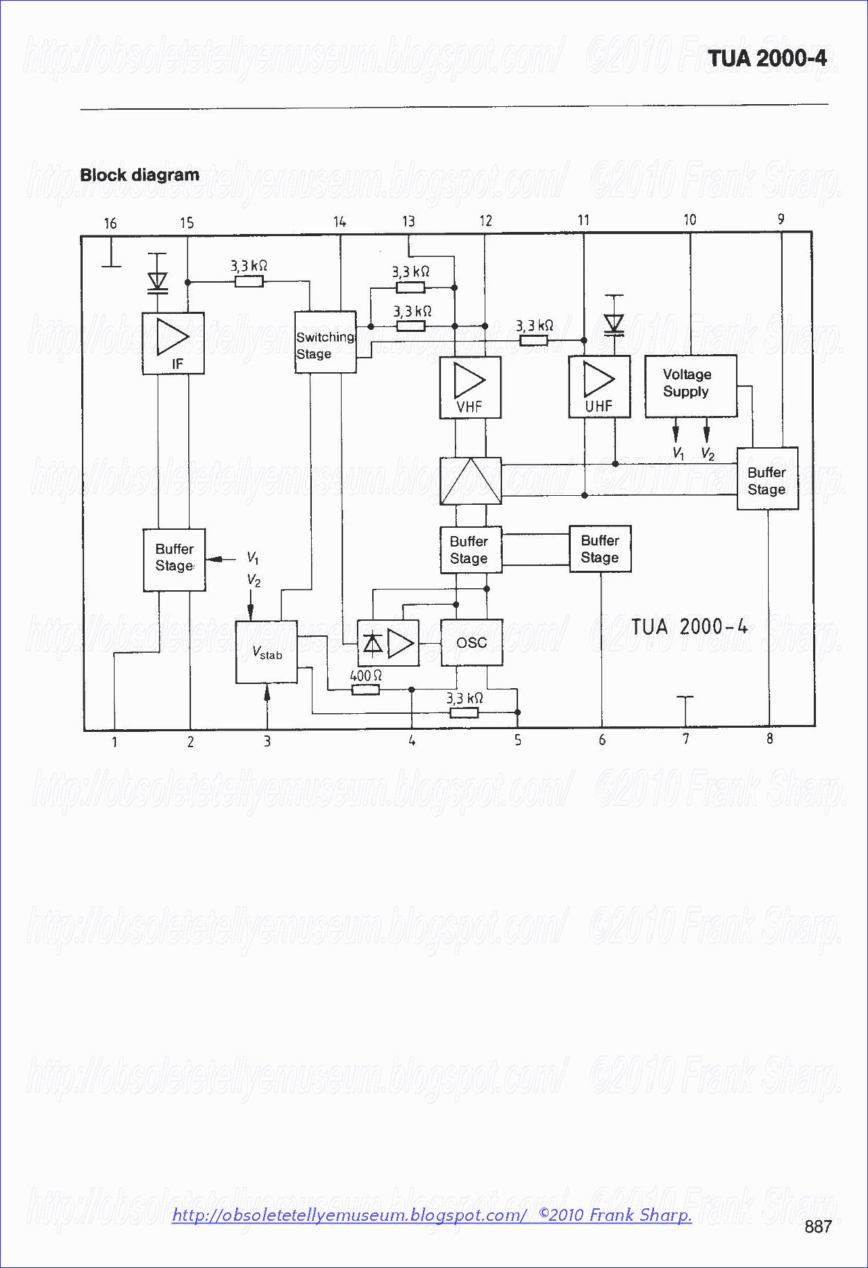


SDA3202-2
General Purpose Phase Locked Loop Device - VCO tuner combo PLL, I2C Bus.


SDA2516 EAROM
Features
- Word-organized reprogrammable nonvolatile memory
in n-channel floating-gate technology (E2PROM)
- 128 ´ 8-bit organization
- Supply voltage 5 V
- Serial 2-line bus for data input and output (I2C Bus)
- Reprogramming mode, 10 ms erase/write cycle
- Reprogramming by means of on-chip control (without
external control)
- Check for end of programming process
- Data retention > 10 years
- More than 104 reprogramming cycles per address
- Compatible with SDA 2516. Exception:
Conditions for total erase and current consumption.
I2C Bus Interface
The I2C Bus is a bidirectional 2-line bus for the transfer of data between various integrated circuits.
It consists of a serial data line SDA and a serial clock line SCL. The data line requires an external
pull-up resistor to VCC (open drain output stage).
The possible operational states of the I2C Bus are shown in figure 1. In the quiescent state, both
lines SDA and SCL are high, i.e. the output stage of the data line is disabled. As long a SCL remains
"1", information changes on the data bus indicate the start or the end of data transfer between two
components.
The transition on SDA from "1" to "0" is a start condition, the transition from "0" to "1" a stop
condition. During a data transfer the information on the data bus will only change while the clock line
SCL is "0". The information on SDA is valid as long as SCL is "1".
In conjunction with an I2C Bus system, the memory component can operate as a receiver and as a
transmitter (slave receiver or slave transmitter). Between a start and stop condition, information is
always
transmitted in byte-organized form. Between the trailing edge of the
eighth clock pulse and a ninth acknowledge clock pulse, the memory
component sets the SDA line to low as a confirmation
of reception, if the chip select conditions have been met. During the output of data, the data output
of the memory is high in impedance during the ninth clock pulse (acknowledge master).
The signal timing required for the operation of the I2C Bus is summarized in figure 2.
Control Functions of the I2C Bus
The memory component is controlled by the controller (master) via the I2C Bus in two operating
modes: read-out cycle, and reprogramming cycle, including erase and write to a memory address.
In both operating modes, the controller, as transmitter, has to provide 3 bytes and an additional
acknowledge clock pulse to the bus after the start condition. During a memory read, at least nine
additional clock pulses are required to accept the data from the memory and the acknowledge
master, before the stop condition may follow. In the case of programming, the active programming
process is only started by the stop condition after data input (see figure 3).
The chip select word contains the 3 chip select bits CS0, CS1 and CS2, thus allowing 8 memory
chips to be connected in parallel. Chip select is achieved when the three control bits logically
correspond to the selected conditions at the select inputs.
Check for End of Programming or Abortion of Programming Process
If the chip is addressed during active reprogramming by entering CS/E, the programming process
is terminated. If, however, it is addressed by entering CS/A, the entry will be ignored. Only after
programming has been terminated will the chip respond to CS/A. This allows the user to check
whether the end of the programming process has been reached (see figure 3).
Memory Read
After the input of the first two control words CS/E and WA, the resetting of the start condition and the
input of a third control word CS/A, the memory is set ready to read. During acknowledge clock
nine, the memory information is transferred in parallel mode to the shift register. Subsequent to the
trailing edge of the acknowledge clock, the data output is low impedance and the first data bit can
be sampled, (see figure 4).
With every shift clock, an additional bit reaches the output. After reading a byte, the internal address
counter is automatically incremented when the master receiver switches the data line to “low” during
the ninth clock (acknowledge master). Any number of memory locations can thus be read one after
the other. At address 128, an overflow to address 0 is not initiated. With the stop condition, the data
output returns to high-impedance mode. The internal sequence control of the memory component
is reset from the read to the quiescent with the stop condition.
Memory Reprogramming
The reprogramming cycle of a memory word comprises an erase and a subsequent write process.
During erase, all eight bits of the selected word are set into "1" state. During write, "0" states are
generated according to the information in the internal data register, i.e. according to the third input
control word.
After the 27th and the last clock of the control word input, the active programming process is started
by the stop condition. The active reprogramming process is executed under onchip control.
The time required for reprogramming depends on component deviation and data patterns.
Therefore, with rated supply voltage, the erase/write process extends over max. 20 ms, or more
typically, 10 ms. In the case of data word input without write request (write request is defined as data
bit in data register set to “0”), the write process is suppressed and the programming time is
shortened. During a subsequent programming of an already erased memory address, the erase
process is suppressed again, so that the reprogramming time is also shortened.
PHILIPS TDA2595 Horizontal combination
GENERAL DESCRIPTION
The TDA2595 is a monolithic integrated circuit intended for use in colour television receivers.
Features
• Positive video input; capacitively coupled (source impedance < 200 Ω)
• Adaptive sync separator; slicing level at 50% of sync amplitude
• Internal vertical pulse separator with double slope integrator
• Output stage for vertical sync pulse or composite sync depending on the load; both are switched off at muting
• φ1 phase control between horizontal sync and oscillator
• Coincidence detector φ3 for automatic time-constant switching; overruled by the VCR switch
• Time-constant switch between two external time-constants or loop-gain; both controlled by the coincidence detector φ3
• φ1 gating pulse controlled by coincidence detector φ3
• Mute circuit depending on TV transmitter identification
• φ2 phase control between line flyback and oscillator; the slicing levels for φ2 control and horizontal blanking can be set
separately
• Burst keying and horizontal blanking pulse generation, in combination with clamping of the vertical blanking pulse
(three-level sandcastle)
• Horizontal drive output with constant duty cycle inhibited by the protection circuit or the supply voltage sensor
• Detector for too low supply voltage
• Protection circuit for switching off the horizontal drive output continuously if the input voltage is below 4 V or higher
than 8 V
• Line flyback control causing the horizontal blanking level at the sandcastle output continuously in case of a missing
flyback pulse
• Spot-suppressor controlled by the line flyback control
SIEMENS TV Stereo Decoder with Matrix TDA6600-2
Preliminary Data Bipolar IC:
The TDA6600-2 includes an advanced decoder for the identification signals for the
multichannel TV sound systems according to the dual-carrier system as well as a matrix
switched by the decoder to provide the L-Ft-information.
Features
0 Increased switching reliability and recognition by means of two PLLs for stereo
(117 Hz) and / or dual channel (274 Hz)
0 Separate bandwidth selection for dual-tone (pins 17-18) and stereo (pins 14-15)
0 Separate setting for the PLL time constants for dual-tone (pin 10) and stereo (pin 11)
0 Adjustable cut level for dual-tone (pin 8) and stereo (pin 9)
0 Cross-talk rejection independent of external component accuracy
0 Adjustment to minimal cross-talk level through external DC voltage
0 Suitable for TV sets with a 15625-Hz signal.
Type Ordering Code Package
TDA 6600-2 Q67000-A8210 P-DlP-24
Circuit Description
The circuitry has two functional sections:
Two phase locked loops for generating the required comparison frequencies (54.96
kHz and 54.8 kHz) from the line frequency. The phase detectors of the control loops
operate in a frequency range of 117 Hz and/or 274 Hz.
Four demodulators to evaluate the 54-kHz pilot signal. The capacitors at the mixer
outputs determine the bandwidth (and thus the signal-to-noise ratio) of the pilot tone
recognition.
An evaluation circuitry for decoding "stereo", "dual sound", and "mono" from the mixer
output levels. ln order to assure interference-free operation in case of high noise level
input signals, the individual signals "stereo" and "dual sound" are delayed via an
externally adjustable integrator. The subsequent digital evaluation provides the
information "mono", "dual sound", or "stereo" to the matrix and the 4 level input/output
(to drive the TDA 6200). If this four level input/output is connected to ground externally
(e.g. by the TDA 6200), the decoder will recognize this signal as "forced mono".
A stereo matrix with deemphasis and SCART output switched by the pilot frequency
decoder. The SCART output can be disabled by a MUTE signal (coincidence).


SIEMENS TDA6200 TV Stereo Tone Control IC with Quasi-Stereo Section,
Channel 1/2 Switch, SCART Input, and I2C Bus Control
Features
0 Treble, bass, balance, and volume control by means of an integrated digital-to-analog
converter
I Quasi~stereo circuit during mono operation
0 Stereo basewidth expansion during stereo operation
O Physiological volume control
I Channel 1/2 switch-over during dual audio transmission
0 SCART connection
0 Control of all functions via the IZC bus and the bidirectional 4 level line of the
TDA 6600-2 (stereo demodulator IC)
O LED driver
0 Volume control range 80 dB
0 Treble, bass control 1 ‘I2 dB
O Channel separation min. 60 dB, cross-talk rejection min. 60 dB
O Parasitic voltage spacing up to 78 dB
Type W W Ordering Code Package
TDA 6200 Q67000-A2461 P-DIP-28
The TDA 6200 is comprised of a SCART switch-over, channel 1/2 switch-over, quasi-
stereo circuit, stereo basewidth expansion, physiological volume control, a treble, bass,
and volume control of the injected AF signals as well as an LED driver. The IC is
controlled by means of an FC bus serial interface as well as by the bidirectional 4 level
line from the TDA 6600-2. The component is used for AF sound signal processing in
stereo TV sets.


SIEMENS TDA5830 Video IF IC with VTR Connection TDA5830-2 and Quasi-Parallel Sound
Bipolar IC
Video IF Section
Controlled AM broadband amplifier with synchronous demodulator, video amplifier, VTR
input and output, and AGC voltage generation for the video IF amplifier and tuner.
Quasi-Parallel Sound Section
Controlled AM broadband amplifier with quadrature demodulator, sound carrier output,
and internal AGC voltage generation.
The TDA 5830-2 is especially suitable for application with black and white or color
television receivers and/or VTFI systems with PNP/MOS tuners for TV standards with
negative video modulation and FM sound.
Type Ordering Code Package
TDA 5830-2 067000-A2504 P-DIP-22
Circuit Description
The video IF section is comprised of a 4-stage controllable AM amplifier, a limiter, and a
mixer for the synchronous demodulation of video signals as well as an amplifier for the
positive video output signal.
The positive video signal is used for gated control. In addition, the IC includes a standard
VTR connection via an external transistor. The delayed tuner AGC is generated by a
threshold amplifier driven by the control voltage.
The quasi-parallel sound section also includes a 4-stage AM amplifier, a limiter, and a
mixer for the quadrature demodulation of the 1st sound IF with subsequent sound carrier
output for the 2nd sound IF. The control voltage is generated by a peak value rectifier from
the 1st sound IF signal.
Alignment Procedures
a) Video IF
At a video carrier input level of V15/I67l'TIS = 10 mV and a superimposed AGC voltage of Via
= 3 V, the demodulator tank circuit is preliminary aligned so that the demodulated video
signal Vii pp reaches its maximum output level at the positive video output. Any suitable
video test signal can be used for modulation. Subsequently, the AGC voltage V13 is
reduced until the video signal equals approx. 3 V (peak-to-peak). By fine-aligning the
demodulator tank circuit, the maximum output level of the video signal is reached. The flat
response characteristic of the demodulator ensures a non-critical alignment procedure.
b) OPS
At an input signal of V‘8l1Q mis = 10 mV, the demodulator tank circuit is preliminarily aligned
until a max. AM suppression of the demodulated video signal Vzi is reached at the sound
carrier output. A video signal critical for the sound-interference ratio should be used for
modulation (white/staircase, FuBK). Subsequent tine-aligning is performed by measuring
the sound—interference ratio at the output of a FM demodulator and fine-aligning the
demodulator tank circuit for a max. interference ratio. If several sound carriers are used in
a device, the sound carrier with the lowest level should be used for alignment purposes.


TDA4555 Multistandard decoder
GENERAL DESCRIPTION
The TDA4555 and TDA4556 are monolithic integrated
multistandard colour decoders for the PAL, SECAM,
NTSC 3,58 MHz and NTSC 4,43 MHz standards. The
difference between the TDA4555 and TDA4556 is the
polarity of the colour difference output signals (B-Y)
and (R-Y).
Features
Chrominance part
· Gain controlled chrominance amplifier for PAL, SECAM
and NTSC
· ACC rectifier circuits (PAL/NTSC, SECAM)
· Burst blanking (PAL) in front of 64 ms glass delay line
· Chrominance output stage for driving the 64 ms glass
delay line (PAL, SECAM)
· Limiter stages for direct and delayed SECAM signal
· SECAM permutator
Demodulator part
· Flyback blanking incorporated in the two synchronous
demodulators (PAL, NTSC)
· PAL switch
· Internal PAL matrix
· Two quadrature demodulators with external reference
tuned circuits (SECAM)
· Internal filtering of residual carrier
· De-emphasis (SECAM)
· Insertion of reference voltages as achromatic value
(SECAM) in the (B-Y) and (R-Y) colour difference output
stages (blanking)
Identification part
· Automatic standard recognition by sequential inquiry
· Delay for colour-on and scanning-on
· Reliable SECAM identification by PAL priority circuit
· Forced switch-on of a standard
· Four switching voltages for chrominance filters, traps
and crystals
· Two identification circuits for PAL/SECAM (H/2) and
NTSC
· PAL/SECAM flip-flop
· SECAM identification mode switch (horizontal, vertical
or combined horizontal and vertical)
· Crystal oscillator with divider stages and PLL circuitry
(PAL, NTSC) for double colour subcarrier frequency
· HUE control (NTSC)
· Service switch
PHILIPS TDA3505 Video control combination circuit with automatic cut-off control
GENERAL DESCRIPTION
The TDA3505 and TDA3506 are monolithic integrated circuits which perform video control functions in a PAL/SECAM
decoder. The TDA3505 is for negative colour difference signals -(R-Y), -(B-Y) and the TDA3506 is for positive colour
difference signals +(R-Y), +(B-Y).
The required input signals are: luminance and colour difference (negative or positive) and a 3-level sandcastle pulse for
control purposes. Linear RGB signals can be inserted from an external source. RGB output signals are available for
driving the video output stages. The circuits provide automatic cut-off control of the picture tube.
Features
· Capacitive coupling of the colour difference and
luminance input signals with black level clamping in the
input stages
· Linear saturation control acting on the colour difference
signals
· (G-Y) and RGB matrix
· Linear transmission of inserted signals
· Equal black levels for inserted and matrixed signals
· 3 identical channels for the RGB signals
· Linear contrast and brightness controls, operating on
both the inserted and matrixed RGB signals
· Peak beam current limiting input
· Clamping, horizontal and vertical blanking of the three
input signals controlled by a 3-level sandcastle pulse
· 3 DC gain controls for the RGB output signals (white
point adjustment)
· Emitter-follower outputs for driving the RGB output
stages
· Input for automatic cut-off control with compensation for
leakage current of the picture tube.
philips TDA4565 Colour transient improvement circuit
GENERAL DESCRIPTION
The TDA4565 is a monolithic integrated circuit for colour transient improvement (CTI) and luminance delay line in gyrator
technique in colour television receivers.
Features
· Colour transient improvement for colour difference signals (R-Y) and (B-Y) with transient detecting-, storage- and
switching stages resulting in high transients of colour difference output signals
· A luminance signal path (Y) which substitutes the conventional Y-delay coil with an integrated Y-delay line
· Switchable delay time from 730 ns to 1000 ns in steps of 90 ns and additional fine adjustment of 50 ns
· Two Y output signals; one of 180 ns less delay.
PHILIPS SAA5231 Teletext video processor.
GENERAL DESCRIPTION
The SAA5231 is a bipolar integrated circuit intended as a successor to the SAA5030. It extracts Teletext Data from the
video signal, regenerates Teletext Clock and synchronizes the text display to the television syncs. The integrated circuit
is intended to work in conjunction with CCT (Computer Controlled Teletext), EUROM or other compatible devices.
Features
• Adaptive data slicer
• Data clock regenerator
• Adaptive sync separator, horizontal phase detector and 6 MHz VCO forming display phase locked loop (PLL)
The function is quoted against the corresponding pin number.
1. Synch output to TV
Output with dual polarity buffer, a load resistor to 0 V or + 12 V selects positive-going or negative-going syncs.
2. Video input level select
When this pin is LOW a 1 V video input level is selected. When the pin is not connected it floats HIGH selecting a
2,5 V video input level.
3. HF filter
The video signal for the h.f.-loss compensator is filtered by a 15 pF capacitor connected to this pin.
4. Store h.f.
The h.f. amplitude is stored by a 1 nF capacitor connected to this pin.
5. Store amplitude
The amplitude for the adaptive data slicer is stored by a 470 pF capacitor connected to this pin.
6. Store zero level
The zero level for the adaptive data slicer is stored by a 22 nF capacitor connected to this pin.
7. External data input
Current input for sliced teletext data from external device.
Active HIGH level (current), low impedance input.
8. Data timing
A 270 pF capacitor is connected to this pin for timing of the adaptive data slicer.
9. Store phase
The output signal from the clock phase detector is stored by a 100 pF capacitor connected to this pin.
10. Video tape recorder mode (VCR)
Signal input to command PLL into short time constant mode. Not used in application circuit Fig.4a or Fig.4b.
11. Crystal
A 13,875 MHz crystal, 2 x data rate, connected in series with a 15 pF capacitor is applied via this pin to the oscillator
and divide-by-two to provide the 6,9375 MHz clock signal.
12. Clock filter
A filter for the 6,9375 MHz clock signal is connected to this pin.
13. Ground (0 V)
14. Teletext clock output (TTC)
Clock output for CCT (Computer Controlled Teletext).
15. Teletext data output (TTD)
Data output for CCT.
16. Supply voltage VCC (+ 12 V typ.)
17. Clock output (F6)
6 MHz clock output for timing and sandcastle generation in CCT.
18. Oscillator output (6 MHz)
A series resonant circuit is connected between this pin and pin 20 to control the nominal frequency of the VCO.
19. Filter 2
A filter with a short time constant is connected to this pin for the horizontal phase detector. It is used in the video
recorder mode and while the loop is locking up.
20. Oscillator input (6 MHz)
See pin 18.
21. Filter 1
A filter with a long time constant is connected to this pin for the horizontal phase detector.
22. Sandcastle input pulse (PL/CBB)
This input accepts a sandcastle waveform, which is formed from PL and CBB from the CCT.
Signal timing is shown in Fig.5.
23. Pulse timing resistor
The current for the pulse generator is defined by a 68 Ω resistor connected to this pin.
24. Pulse timing capacitor
The timing of the pulse generator is determined by a 220 pF capacitor connected to this pin.
25. Video composite sync output (VCS)
The output signal is for CCT.
26. Black level
The black level for the adaptive sync separator is stored by a 68 nF capacitor connected to this pin.
27. Composite video input (CVS)
The composite video signal is input via a 2,2 μF clamping capacitor to the adaptive sync separator.
28. Text composite sync input (TCS)/Scan composite sync input (SCS)
TCS is input from CCT or SCS from external sync circuit. SCS is expected when there is no load resistor at pin 1.
If pin 28 is not connected the sync output on pin 1 will be the composite video input at pin 27, internally buffered.
GRUNDIG SUPER COLOR M55-355A CTI CHASSIS CUC3510 Television device with processing of teletext signals:
VT (GB: Teletext) instalation and matching adjustment
When fitting the Videotext (GB: Teletext) plug-in board, the Videotext plug plate has to be removed
The
control R 2857 is set in the fully anti clockwise position when the
unit is delivered (smallest treble boost: approx. 2 dB). If, with a
perfect aerial signal character faults occur, turn R 2857 slowly
clockwise until the faults disappear. Do not turn R 2875 up any further as error rate may increase again.
Page
199 must always be selected anew during the adjustment, as Oniy this
effects a new read-in of the page making it possible to evaluate the
error level.
The present invention relates to television receivers with processing of teletext signals transmitted during a teletext transmission period of several video lines within a vertical blanking period.
A television system may include additional transmission of a digital teletext signal that is transmitted during one or more video lines of the vertical flyback period. The digital teletext signal is decoded in the receiver is decoded for producing additional control signals for the picture tube for teletext display. Such teletext processing circuits may include a sine wave clock oscillator synchronized by the teletext signal. The oscillator produces a substantially sine wave clock signal which is coupled to a synchronizing or triggering input of a logic circuit that processes the teletext signal. The logic circuit produces one or more data synchronizing clock and data signals used for teletext signal processing.
The output signal of the clock oscillator is substantially a sine wave and has substantially no harmonics. Therefore, the output signal may not cause significant interference within the reproduced picture.
The output signals of the logic circuit, however, have very fast transition times, especially in connection with miniaturized circuit elements. That means that these signals include high harmonics of substantial amplitude. The high harmonies tend to cause interferences within the reproduced picture. If, for example, the frequency of the clock oscillator is 55 MHz, than the 10th harmonic within the clock and data signals, that is 550 MHz, lies within the UHF-band.
It may be desirable to avoid the interferences within the reproduced picture due to high harmonics within the clock and data signals produced by the logic circuit.
In accordance with an aspect of the invention, the amplitude of the oscillator output signal that is coupled to the logic circuit is reduced during an interval, within a vertical field period, in which the logic circuit is not required to process teletext data.
The invention is based upon the
following consideration. The teletext signal is present only during one
or more video lines of the vertical blanking period. It follows that
the clock and data signals need not he produced for further processing
of the teletext data at any other time, especially during the full
vertical forward scan period. Therefore, it is possible to disable the
logic circuit outside the interval in which teletext data is processed,
herein referred to as the teletext data transmission period, in order to
avoid the interference. On the other hand, during the teletext data
transmission period, the clock and data signals are needed and do not
produce interferences. Interferences are not produced because, during
the teletext data transmission period, no picture is produced as a
result of vertical flyback and blanking.
By switching off the
logic circuit outside the teletext data transmission period, the
aforementioned interference is avoided in a very simple manner.
A teletext decoder includes a background or buffer memory operating as a
first-in, first-out (FIFO) memory. The buffer memory is used for
storing a large number of teletext pages. A given video line that
contains teletext information is identified as such by the detection of
part of a clock run-in sequence followed by the framing code. The video
line is then stored in the background memory. After a user page request
occurs, the background memory is read-out by a data processor operating
in a full channel mode of operation for obtaining the information of the
requested page. As long as the read-out operation has not been
terminated, incoming teletext data is stored in the background memory.
This enables teletext data received prior to termination of the read-out
operation to be read out and processed by the data processor.
Other References:
A data sheet for teleview data acquisition chip MR9710, published by Plessey Semiconductors Ltd., pp. 59-65.
Data
sheet for videotext data slicer and clock regenerator SL9100EXP, publ.
by Plessey Semiconductors Ltd. (Attention to Fig. 4).
"Applications
of Picture Memories in Television Receivers", Berkhoff, et al.,
published in IEEE Transactions on Consumer Electronics, vol. CE-29, No.
3, Aug. 1983.
Philips publication No. 9398 401 30011, dated Jan.
1985, entitled "ICS for Computer Controlled TV Memory Based Feature",
pp. 27-41.
Development data sheet, dated 1986, entitled "SAA9030 Background Memory Controller", published by Philips Corp.
Development data sheet, dated 1988, entitled "SAA9040 Computer Controlled Teletext Extension (CCTE)", published by Philips Corp.
User's
Manual, entitled "Computer Controlled Teletext User's Manual", dated
1983, by J. R. Kinghorn, published by Mullard Application Laboratory.
IBA Technical Review, No. ISSN 0308-423 X entitled "Specification of Standard for Broadcast Teletext Signals."
Design
Handbook entitled "The Programmable Gate Array Design Handbook", dated
1986, published by Xilinx Co., San Jose, California, pp. 2-114 to 2-117.
Data
Book Entitled "the Programmable Gate Array Data Book", including a note
entitled Megabit FIFO in two Chips: One LCA and One Dram, by Alfke,
published 1988 by Xilinx Co., pp. 6-35 and 6-36.
GRUNDIG SUPER COLOR M55-355A CTI CHASSIS CUC3510 Rapid access teletext - Videotextx decoder arrangement:A teletext decoder includes a background or buffer memory operating as a first-in, first-out (FIFO)
memory. The buffer memory is used for storing a large number of
teletext pages. A given video line that contains teletext information
is identified as such by the detection of part of a clock run-in
sequence followed by the framing code. The video line is then stored in
the background memory. After a user page request occurs, the
background memory is read-out by a data processor operating in a full
channel mode of operation for obtaining the information of the
requested page. As long as the read-out operation has not been
terminated, incoming teletext data is stored in the background memory.
This enables teletext data received prior to termination of the read-out
operation to be read out and processed by the data processor.
1.
A television apparatus responsive to an incoming television signal
containing video lines that carry text data, defining corresponding
data lines, for generating an output signal that is capable of
providing picture information to a display device, comprising:
means
for generating a first control signal in order to select one of said
data lines to be used in conjunction with the generation of said output
signal;
a source of said television signal;
a first-in, first-out background memory having a data input that is coupled to an output of said source;
first
control means coupled to said background memory for controlling
storage therein of corresponding data lines of said television signal,
wherein prior to the time said first control signal is generated, said
background memory already contains a substantial number of stored data
lines of said television signal;
second control means responsive
to said first control signal and coupled to said background memory for
controlling during a given interval that follows the generation of
said first control signal, read-out from said background memory of a
plurality of data lines of said television signal that have been stored
before the end of said given interval, said given interval having a
duration that is substantially shorter than that of a corresponding
interval between the occurrence of an initial data line of said
plurality of data lines and the occurrence of a final data line thereof
so as to reduce access time to said plurality of data lines, said
second control means controlling read-out of said plurality of data
lines in a first-in, first-out manner for generating during said given
interval a data signal that contains the data of said plurality of data
lines including data lines that have been stored in said background
memory during said given interval; and
a data processor
responsive to said data signal for selecting said one data line to
generate in accordance therewith said output signal.
2. An
apparatus according to claim 1 wherein said data lines occur in said
television signal only during, corresponding vertical blanking
intervals, wherein, during said given interval, said data processor
operates in a full channel mode of operation, and wherein, prior to the
time when said first control signal is generated, said data processor
operates in a field flyback mode of operation.
3. An apparatus according to claim 1 further comprising,
means for coupling said data signal and said television signal to said
data processor such that prior to the time said first control signal is
generated said television signal is coupled to said data processor in a
manner that bypasses said background memory.
4. An apparatus according to claim 3 wherein, throughout
said given interval, said coupling means decouples said signal that
bypasses said background memory from said data processor.
5. An apparatus according to claim 1 further
comprising, a switch having a first input that is coupled between said
output of said source of said television signal and said data input of
said background memory, a second input that is coupled to a data output
of said background memory and a switch output that is coupled to an
input of said data processor. 6.
An apparatus according to claim 5 further comprising, means for
generating a second control signal that is coupled to a control input
of said switch, said second control signal having a first state for
enabling said switch to couple the signal that is developed at said
second input of said switch to said data processor following the time
when said first control signal is generated and having a second state,
for enabling said switch to couple the signal that is developed at said
first input thereof to said data processor following the occurrence of
the earlier of (a) a time when all the data stored in said background
memory has been read out, and (b) a time when a first time-out interval
has elapsed from a time when said data processor selects the data of a
Page Header data line. 7. An
apparatus according to claim 5 further comprising, means coupled to
said background memory, for generating, in accordance with the data of
said plurality of data lines, a serial bit data signal that contains
corresponding data lines that are read out of said background memory in
a first-in, first-out manner, said serial bit data signal being
coupled to said second input of said switch, said switch coupling said
serial bit data signal to said input of said data processor, during
said given interval, and coupling the signal that is developed at said
first input of said switch to said input of said data processor, outside
said given interval. 8. An
apparatus according to claim 1 wherein, as a result of reading out the
data of said plurality of data lines in the first-in, first-out manner,
memory addresses, where said plurality of data lines are stored in
said background memory are transparent to the operation of said data
processor. 9. An apparatus
according to claim 1 wherein said data processor is included in an
integrated circuit of the same type used in a conventional teletext
decoder such that said background memory provides an add-on feature.
10. An apparatus according to claim 1
wherein said television signal comprises a teletext signal and wherein
said television apparatus comprises a teletext decoder.
11. An apparatus according to claim 10 wherein
said data lines of said television signal define corresponding pages of
teletext data, wherein said background memory is capable of containing
at a given time the data of a substantial number of said pages and
wherein, during said given interval, said data processor selects from
the data that is read out of said background memory the data of a first
page, in accordance with said one of said data lines that is a
Page-Header data line, to generate from the data of said first page
said output signal. 12. An
apparatus according to claim 1 further comprising, a page memory
wherein said output signal is stored in said page memory during said
given interval. 13. An apparatus
according to claim 1 further comprising, a switch for coupling one of
said data signal that is generated at an output of said background
memory and a second data signal, that bypasses said background memory,
to an input of said data processor when a second control signal that is
developed at a control input of said switch is at first state and for
coupling the other one of said to said input of said data processor
when said second control signal is at a second state.
14. An apparatus according to claim 13 further
comprising, means for generating, during said given interval, a first
time-out signal after an interval having a predetermined duration has
elapsed from a time when the data of said one of said data line that is
a Page Header data line has been identified in said data signal and
means responsive to said first time-out signal for generating said
second control signal in accordance with said first time-out signal .
15. An apparatus according to
claim 13 further comprising, means for generating a signal that is
indicative
of when the data of all the da&a lines that are stored in said
background memory have been read out and that is coupled to said
control input of said switch to control the state of said second
control signal. 16. A television
apparatus according to claim 1 wherein said data processor is
responsive, outside said given interval, to data lines of said
television signal that are coupled to said data processor in a manner
that bypasses said background memory.
17. An apparatus according to claim 1 further comprising, a
parallel-to-serial converter that is coupled between an output of said
background memory and an input of said data processor.
18. A television apparatus according to claim 1
wherein said background memory comprises a random access memory,
wherein said first control means comprises first sequencing means that
is coupled to an address input of said random access memory for
generating a write-in address word and wherein said second control
means comprises second sequencing means for generating a read-out
address word that is coupled to said address input.
19. An apparatus according to claim 18 wherein at
least one of said first and second sequencing means comprises a linear
feedback shift register counter.
20. An apparatus according to claim 18 wherein each of said data lines
includes a corresponding plurality of data line portions that are
stored in corresponding locations in said background memory having
corresponding addresses, wherein said first sequencing means changes
states in a cyclical manner each time a given one of said portions of
each data line is stored such that the number of states in each cycle is
equal to an integer multiple of the total number of data lines that
can be stored in said background memory in each cycle.
21. An apparatus according to claim 20 wherein
the number of memory addresses that are required for storing a given
data line is equal to 86. 22. An
apparatus according to claim 20 wherein the number of said states in
each cycle is equal to. 23. A
television apparatus according to claim 1 further comprising, a page
memory responsive to said output signal for storing said output signal
therein. 24. An apparatus
according to claim 1 wherein said data processor operates in a full
channel mode of operation throughout said given interval and wherein
said television signal contains said data lines only during
corresponding vertical blanking intervals thereof.
25. An apparatus according to claim 1 wherein said
first control means identifies, in a given video line signal, data of a
clock run-in portion of said video line signal and stores in said
background memory text data of such video line signal provided that
said data of said clock run-in portion is identified.
26. An apparatus according to claim 25 wherein said
said first control means identifies said given data line also in
accordance with data of a framing code.
27. An apparatus according to claim 1 wherein said first control
signal is indicative of when a user initiated page request has occurred
and causes said data processor to operate in a full channel mode of
operation during said given interval.
28. An apparatus according to claim 27 further comprising, means
for generating a second control signal that is indicative when a
predetermined time-out interval has elapsed from the time said first
control signal is generated, said second control signal being coupled to
said data processor for causing said data processor to start operating
in a field flyback mode of operation following said time-out interval
irrespective of whether said one of said data lines that is a Page
Header of the page requested has been selected.
29. An apparatus according to claim 28 wherein said
second control signal is generated in a microprocessor such that said
time out interval is determined by a program thereof.
30. A television apparatus responsive to an
incoming television signal containing video line signals that carry
text data, defining corresponding data lines, for generating an output
signal that is capable of providing picture information to a display
device, comprising: means for generating a first control signal in order to select one of said data lines to be used in conjunction with the generation of said output signal;
a source of said television signal;
a first-in, first-out background memory having a data input that is coupled to said source;
first control means coupled to said background memory for controlling storage therein of corresponding data lines of said television signal, wherein prior to the time said first control signal is generated, said background memory already contains a substantial number of stored data lines of said television signal;
second control means responsive to said first control signal and coupled to said background memory for controlling during a given interval that follows the generation of said first control signal, read-out from said background memory of a plurality of stored data lines of said television signal, such that the duration of said given interval is substantially shorter than that of a corresponding interval between the occurrence of an initial data line of said plurality of data lines and the occurrence of a final data line thereof, so as to reduce access time to said plurality of data lines, said second control means controlling read-out of said plurality of data lines in a first-in, first-out manner for generating during said given interval a data signal that contains the data of said plurality of data lines;
a switch having a first input that is coupled to said source of said television signal, having a second input that is coupled to a data output of said background memory and having an output for generating a second data signal;
a data processor responsive to said second data signal for selecting said one data line to generate in accordance therewith said output signal; and
means for generating a second control signal that is coupled to a control input of said switch, said second control signal having a first state for enabling said switch to couple to said data processor after said first control signal is generated the signal that is developed at said switch second input, and having a second state for enabling said switch to couple to said data processor the signal that is developed at said first switch input following the occurrence of the earlier of (a) a time when all the data stored in said background memory has been read out, and (b) a time when a time-out interval has elapsed from a time when said data processor selects said one data line that is a Page Header.
31. A television apparatus responsive to an incoming television signal containing video lines that carry text data, defining corresponding data lines, for generating an output signal that is capable of providing picture information to a display device, comprising:
first means for generating a first control signal in order to select one of said data lines to be used in conjunction with the generation of said output signal;
second means responsive to said television signal for generating a clock signal that is indicative of timings of individual bits of a data sequence of a clock run-in portion of a data line;
a source of said television signal;
a first-in, first-out background memory having a data input that is coupled to said source;
third means coupled to said background memory and responsive to said television signal and to said clock signal for identifying in a given video line, said data sequence of said clock run-in portion of said data line and for storing in said background memory such video lines that are identified as data lines but only when individual bits of said data sequence of said clock run-in portion are correct, said first means storing said data lines such that prior to the generation of said first control signal, said background memory already contains a substantial number of stored data lines of said television signal;
fourth means responsive to said first control signal and coupled to said background memory for controlling during a given interval that follows the generation of said first control signal, read-out from said background memory of a plurality of stored data lines of said television signal, suc
h that the duration of said given interval is substantially
shorter than that of a corresponding interval between the occurrence
of an initial data line of said plurality of data lines and the
occurrence of a final data line thereof, so as to reduce access time to
said plurality of data lines, said fourth means controlling read-out
of said plurality of data lines in a first-in, first-out manner for
generating during said given interval, a data signal that contains the
data of said plurality of data lines; and a data processor responsive to said data signal for selecting said one data line to generate in accordance therewith said output signal.
32. An apparatus according to claim 31 wherein said third means identifies said video line as data line when data sequence of a framing code portion immediately follows said data sequence of said clock run-in portion. 33. An apparatus according to claim 31 wherein said third means identifies said video line as data line by identifying a 12 bit sequence (101011100100) in data that are derived from said video line.
This
invention relates to a teletext decoder employing a so-called
background or buffer memory for storing multipages of teletext incoming
data. Teletext is a television-based communication technique in which a given horizontal video line is utilized for broadcasting textual and graphical information encoded in a digital binary representation. Such horizontal video line signal that contains teletext data is referred to herein as a Data-line. It is assumed herein, for explanation purposes, that teletext is sent by the broadcaster only during the vertical blanking interval (VBI), when no other picture information is sent. The organization of the binary information in the broadcast signal is determined by the standard employed by the broadcaster. By way of an example only, references are made herein to a teletext based on a standard referred to by the British Broadcasting Corporation (BBC) as CEEFAX.
Each Data-line carries data synchronizing and address information and the codes for a Row of 40 characters. The synchronizing information includes a clock run-in sequence followed by an 8-bit framing code sequence. Each Data-line contains a 3 bit code referred to as the Magazine number. A teletext Page includes 24 Rows of 40 characters, including a special top Row called the Page-Header. Each ROW is contained in a corresponding Data-line. A user selected Page is intended to be displayed in place of, or added to a corresponding television picture frame. A Magazine is defined to include Pages having Data-lines containing a corresponding Magazine number. The transmission of a selected Page begins with, and includes its Page Header and ends with and excludes the next Page Header of the selected Magazine number. All intermediate Data lines carrying the selected Magazine number relate to the selected Page.
 FIG.
1 illustrates a block diagram of a conventional teletext decoder that
includes an integrated circuit (IC) referred to herein as video input
processor (VIP) such as, for example, of the type SAA5231 made by
Philips Corporation. The VIP receives a baseband composite video signal
VIDEO that contains Data-lines. The VIP performs data slicing, clock
regeneration and timing synchronization functions and generates a serial
data signal DATA and an associated clock signal CLOCK Signals DATA and
CLOCK represent the data contained in the horizontal video lines.
Signals DATA and CLOCK are coupled to a second IC of the decoder,
referred to herein as computer controlled teletext IC (CCT) that
includes a data processor responsive to signals DATA and CLOCK. An
example of such CCT is IC SAA5243 made by Philips Corporation.
FIG.
1 illustrates a block diagram of a conventional teletext decoder that
includes an integrated circuit (IC) referred to herein as video input
processor (VIP) such as, for example, of the type SAA5231 made by
Philips Corporation. The VIP receives a baseband composite video signal
VIDEO that contains Data-lines. The VIP performs data slicing, clock
regeneration and timing synchronization functions and generates a serial
data signal DATA and an associated clock signal CLOCK Signals DATA and
CLOCK represent the data contained in the horizontal video lines.
Signals DATA and CLOCK are coupled to a second IC of the decoder,
referred to herein as computer controlled teletext IC (CCT) that
includes a data processor responsive to signals DATA and CLOCK. An
example of such CCT is IC SAA5243 made by Philips Corporation. The CCT performs data acquisition and interface function with a page memory that is included in the teletext decoder. For example, only a teletext Page requested by the user is derived by the CCT from the serial data and clock signals and stored in the page memory. The CCT also generates video display signals R,G, and B from the teletext data stored in the page memory to provide corresponding drive signals that contain picture information for display in the receiver picture tube (CRT), not shown.
A control microcomputer, not shown in FIG. 1, that is responsive to user initiated commands, generates control and status messages. The messages are coupled via, for example, a standard IIC bus to the CCT, for controlling the operation of the CCT.
A total of, for example, 500 Pages may be periodically transmitted during each interval of 15-45 seconds, depending on the number of Data-lines used for teletext during the VBI. Consequently, if the teletext Page is not already stored in memory when a new user page request occurs, the user may experience a nuisance as a result of waiting a maximum of 15-45 seconds until the requested Page is displayed. It may be desirable to reduce such Page access time. It may also be desirable to utilize in the teletext decoder a standard CCT such that the reduction of the access time is provided as an add-on feature to the teletext decoder.
A teletext decoder, embodying an aspect of the invention, includes a background or buffer memory that is capable of storing multi-Pages of teletext data. The portion of serial data signal DATA generated by the VIP that meets a predetermined identification criteria and, therefore, assumed to represent a Data-line is stored in the buffer memory. At any given time after the operation of the buffer memory is enabled, such as immediately after the user turns on the television receiver, the buffer memory contains, for example, the most recently received teletext Pages. The maximum number of such Pages that can be contained in the buffer memory at any given time is determined by the buffer memory Page storage capacity.
In order to reduce the size of the hardware required to identify each video line that is assumed to be a Data-line, only a limited, rather than a complete identification operation, is initially performed. The complete identification is accomplished in the CCT, during a read-out operation, when the data is read-out of the buffer memory.
In
accordance with a feature of the invention, the limited identification
operation for identifying a given Data-line is accomplished by
identifying in a video line signal data of a sequence of the clock
run-in that is immediately followed by a sequence of the framing code.
When, for example, both sequences are identified it is assumed that a
Data-line is identified. Therefore, a portion of such identified
Data-line that contains relevant data bits is stored in the buffer
memory. Otherwise, the video line information is not stored in the
buffer memory. The inclusion of the test for the data of the clock
run-in sequence, advantageously, reduces the probability that the data
that is stored is, in fact, not a Data-line. When the user's page request occurs, the data processor of the CCT receives the data that have been stored in the buffer memory and searches for the presence of a Data-line representing a Page Header of the requested Page. The search operation that is included in the read-out operation begins when the first data is read out of the buffer memory following the occurrence of the user's page request.
Memory read-out cycles occur between VBI's, when no teletext data is received. If the Page Header of the user requested teletext Page is found in the buffer memory in the course of such memory scan or search operation, the stored data of the Page Header is transferred to the page memory.
During the search operation, the CCT operates in the full channel operation mode. In the full channel operation mode, the Data-lines in the buffer memory are read out and transferred to the page memory in a first-in, first-out manner and without encountering large time gaps. Such large time gaps occur when teletext information is received by th
e CCT only
during the VBI's. Therefore, the search operation occurs faster than if
the Data lines were received, unbuffered, only during the VBI's. For
example, the access time to a teletext Page that is already contained
in a buffer memory capable of storing 500 teletext Pages may be reduced
to, for example, 0.8 seconds that is, advantageously, substantially
shorter than the 15-45 seconds maximum access time, referred to before.
Furthermore, should more than, for example, 600 pages be transmitted,
the access time for a page which, at the time the user page request
occurs, is not already stored in the memory, is reduced by the time
required to fill the buffer memory with teletext data. After the Page Header is identified in the CCT, other Data-lines that are associated with the requested Page and that are stored in the buffer memory are read-out. On the other hand, if no Page Header Data-line of the requested teletext Page is found in the buffer memory in the course of the search operation, the unbuffered data received from the VIP will be coupled, after the end of the search operation, directly to the data processor of the CCT such that the buffer memory is bypassed.
When a buffer memory with large storage capacity is utilized, the read-out operation that was explained before may require a longer interval than the interval between consecutive VBI's. It may be desirable to store incoming Data-lines in the buffer memory that occur during the intervening VBI's prior to the completion of the read-out operation. If such incoming Data-lines of the Page requested by the user were not stored, an undesirable situation might have occurred in which only a partial Page is temporarily displayed on the CRT. Such temporary condition may continue until after the time when the same Page is re-transmitted.
In the teletext decoder, embodying an aspect of
the invention, the read-out operation in the buffer memory occurs only
outside the VBI's. Data-lines are stored in the buffer memory during
the VBI's that occur prior to the completion time of the read-out
operation. Therefore, Data-lines that were stored in the buffer memory
after the read-out operation has been initiated and prior to its
termination may be read-out and processed by the CCT. In this way,
advantageously an incoming Data-line that is included in the teletext
Page that is requested may be processed during the read-out operation Each Data-line is stored in the background memory and provided to the CCT in a format that can be readily processed by the CCT. For example, a Data-line is stored as 344 bits that include a byte containing the framing code, two bytes containing hamming codes and forty bytes containing the remaining data.
The buffer memory of the decoder of the invention is organized as a serial memory such as, for example, a first-in, first-out memory (FIFO). For example, immediately after teletext signal is received in the television receiver, the Data-lines are stored in the FIFO even if no user page request occurs. Thus, at the time the user changes the mode of operation of the television receiver from providing normal picture program to providing teletext information, the most recently received teletext data are already stored in the buffer memory.
The buffer memory may utilize, advantageously, a dynamic random access memory (DRAM) of a large capacity that operates as a FIFO. The DRAM may be refreshed between VBI's. A given storage location of the FIFO may be addressed by a read address pointer during the memory read-out operation and by a write address pointer during the VBI's when memory store-in operation occurs. By using separate read and write address pointers, the aforementioned advantage of storing Data-lines while the read-out operation is incomplete may be realized.
A television apparatus, embodying an aspect of the invention, is responsive t
o an incoming television
signal containing video lines that carry text data, defining
corresponding data lines for generating an output signal that is
capable of providing picture information to a display device. A first
control signal is generated in order to select one of the data lines to
be used in conjunction with the generation of the output signal. A
first-in, first-out background memory has a data input that is coupled
to an output of a source of the television signal. Storage of
corresponding data lines of the television signal in the background
memory occurs each time such corresponding data lines occur. Prior to
the time the first control signal is generated, the background memory
already contains a substantial number of stored data lines of the
television signal. During a given interval that follows the generation
of the first control signal, read-out from the background memory of a
plurality of data lines of the television signal that have been stored
before the end of the given interval occurs. The given interval has a
duration that is substantially shorter than that of a corresponding
interval between the occurrence of the first one of the plurality of
data lines and the occurrence of the last one so as to reduce access
time to the plurality of data lines. Read-out of the plurality of data
lines occurs in a first-in, first-out manner for generating during the
given interval a data signal that contains the data of the plurality of
data lines, including data lines that have been stored in the
background memory during the given interval. A data processor is
responsive to the data signal for selecting the one data line to
generate in accordance therewith the output signal. FIG. 1 illustrates a prior art teletext decoder;
FIG. 2 illustrates a rapid access teletext decoder, embodying a feature of the invention;
FIG. 3 illustrates a diagram that is useful for explaining the operation of a first-in, first-out background memory of FIG. 2;
FIG. 4 illustrates a flow chart that is useful for explaining the operation of the teletext decoder of FIG. 2; and
FIG. 5 illustrates a detail schematic of a linear feedback shift register that is used to provide an address pointer for a background memory of FIG. 2.
 FIG.
2 illustrates a block diagram of a rapid access teletext decoder,
embodying an aspect of an invention. Similar symbols and numerals in
FIGS. 1 and 2 indicate similar items or functions.
FIG.
2 illustrates a block diagram of a rapid access teletext decoder,
embodying an aspect of an invention. Similar symbols and numerals in
FIGS. 1 and 2 indicate similar items or functions. A baseband composite video signal VIDEO of FIGURE 2 is coupled from a video detector, not shown, to a VIP 20, such as, for example, of the type SAA5231. VIP 20 generates from signal VIDEO a serial data signal TTDout at a bit rate of 6.9375 MHz and a corresponding clock signal CLOCK that provides timing information of the bits of signal TTDout. VIP 20 also generates a video composite sync signal VCS derived from signal VIDEO. Signal VCS is coupled to a CCT 30 such as, for example, of the SAA5243 IC type. In turn, CCT 30 generates a signal SAND containing the phase locking and color burst blanking information. Signal SAND is coupled back to VIP 20 to provide horizontal phase-locking information to an oscillator of VIP 20, not shown.
The serial data contained in signal TTDout are coupled to a serial-to-parallel converter 35 that includes a shift register, not shown. Serial-to-parallel converter 35 generates a parallel word 35a that is coupled to an identification unit 40.
In accordance with an aspect of the invention, unit 40 tests for the occurrence, in signal TTDout, of a 12-bit sequence (101011100100) of bits in the data stream, representing a 4-bit clock run-in sequence immediately followed by the framing code. The checking for the occurrence of such 12-bit sequence is performed during a time window of 2.7 microsecond, starting 11.8 microseconds after the leading edge of a horizontal sync portion, not shown, of signal VIDEO. Such checking is done for each video line during the possible teletext lines, 6-22 and 319-335, that occur in the VBI's of the corresponding field portions of signal VIDEO.
When the 12-bit sequence is recognized, it is assumed that the video line represents a Data-line of teletext. After an assumed Data-line is identified, only, for example, 344 bits of the assumed data-line are stored in a buffer memory 45, operating as a FIFO. Advantageously, the checking for the 4-bit clock run-in sequence reduces a probability that nonteletext data of a video line that is not a Data-line will be stored in memory 45.
A timing and control unit 100 receives signals SAND, VCS and CLOCK and generates corresponding control signals that, for example, control the operations associated with memory 45, such as the operation of identification unit 40.
It may be desirable to utilize a DRAM IC of a large storage capacity such as, for example, of the 1,098,586 (2 20 ) bit organization as the main storage element of buffer memory 45. This is so in order to provide a storage capacity for a substantial number of teletext Pages. Also, in order to reduce the cost and power dissipation of memory 45 it may be desirable to utilize DRAM's with slow access or cycle time that are typically less expensive. Therefore, the serial teletext data in signal TTDout is converted by converter 35 to 4-bit parallel words, or nibbles 35b. The bits of each nibble 35b are stored simultaneously in buffer memory 45, organized as, for example, a four-bit-wide DRAM. In this way, the DRAM cycle time may be longer than the teletext bit rate.
For each assumed Data-line, the nibble that is firstly stored in buffer memory 45 corresponds to the most significant nibble of the framing code. Thereafter, the remaining consecutively occurring 85 nibbles are stored. The clock run-in bits need not be stored.
A write counter 55 generates a write address pointer, or word W-COUNT that is coupled via a multiplexer/comparator 60 to an address port 45a of memory 45. FIG. 5 illustrates a combination of a schematic diagram and a block diagram of counter 55 of FIG. 2. Similar numerals and symbols in FIGS. 2 and 5 indicate similar items or functions.
Write counter 55 of FIG. 5 includes a 6-bit conventional binary counter 551 that produces 6 bits, A0-A5, of word W-COUNT. The most significant bit of counter 551, bit A5, is coupled to a corresponding clock input terminal CP of each flip-flop of a conventional 14-bit linear feedback shift register (LFSR) counter 552. Counter 552 includes 14 D-type flip-flops that form a shift register The input to a data input terminal of a first flip-flop 552a in the shift register chain of the flip-flops is formed by applying suitable EXCLUSIVE 0R operations on output signals of the first, third, fifth and fourteenth flip-flops in the shift register chain, in a well known manner.
LFSR counter
552 requires less hardware and is faster than a conventional binary
counter since it avoids the carry propagation associated with the
conventional binary counter. LFSR counter 552 goes through a complete
sequence cycle every 2 14 -1 pulses of bit A5 of binary counter 551. Binary counter 551 goes through a complete sequence cycle every 2 6
clock pulses at an input terminal 551a of counter 551. Consequently,
each of counter 55 and word W-COUNT sequences through a complete
predetermined cyclical sequence every 2 20 -64 clock pulses that occur at input terminal 551a. The address of each nibble that is stored is supplied by word W-COUNT of counter 55 of FIG. 2. The value of word W-COUNT is changed to the next or consecutive value in the predetermined cyclical sequence of counter 55 after each nibble is stored. The number of different values in such cyclical sequence that is, for example, (2 20 -64), is equal to the number of nibble storage locations utilized in memory 45. Therefore, advantageously, each DRAM, having 2 20 locations, is substantially fully utilized. The number (2 20 -64) is equal to an integer multiple of 86, the number of nibbles required for storing the 344 bits of each Data-line. As a result of the FIFO operation, a maximum of (2 20 -64) divided by 86 of the most recently received Data-lines can be stored in buffer memory 45 of FIG. 2.
FIG. 3 illustrates, schematically, the cyclical sequence of word W-COUNT of write counter 55. Similar numbers and symbols in FIGS. 2, 3 and 5 depict similar items or functions. The cyclical sequence includes 2 20 -64 values distributed in a circular manner from a l to a Q where Q=2 20 -64. Thus, for example, after a nibble location, depicted as a n in FIG. 3, is stored in memory 45 of FIG. 2, the next nibble to be stored in memory 45 is stored in a location depicted as a n +1 in FIG. 3, and so forth.
The number of different values in the cyclical sequence of counter 55 of FIG. 2 is equal to an integer multiple of 86. Therefore, Data lines are stored, for example, always in the same corresponding groups of
 86 nibbles of memory 45, such as, for example, a 1 -a 86
of FIG. 3. The most significant nibble of the framing code is stored,
for example, always at the same memory locations of memory 45. This
feature, advantageously, simplifies the hardware complexity of unit 100
of FIG. 2 that controls memory 45.
86 nibbles of memory 45, such as, for example, a 1 -a 86
of FIG. 3. The most significant nibble of the framing code is stored,
for example, always at the same memory locations of memory 45. This
feature, advantageously, simplifies the hardware complexity of unit 100
of FIG. 2 that controls memory 45. FIG. 4 is a flow chart depicting the operation of the teletext decoder of FIG. 2 after a page request for displaying requested Page on a CRT, not shown, is initiated by the user. Similar numerals and symbols in FIGS. 2-5 indicate similar items or functions. A given user page request that is communicated to a microcomputer 65 of FIG. 2 via a keyboard, not shown, causes microcomputer 65 to generate a clear page memory command signal. Such command signal is coupled via a conventional IIC bus to CCT 30. CCT 30 stores in all the memory locations of a page memory 70, in response to the clear page memory command signal, "blank" characters, referred to as page memory clearing operation. After a 22 millisecond interval of the memory clearing operation has elapsed, microcomputer 65 sends a second command signal to CCT 30 that causes CCT 30 to begin operating in a mode of operation referred to as full channel operation mode, as shown in step d of FIG. 4.
In the full channel operation mode, data is received by CCT 30 of FIG. 2 during each video line in a given frame interval of signal VIDEO. In comparison, in normal field flyback operation mode, data is received for processing by CCT 30 only during lines 6-22 and 319-325 of the VBI's of the corresponding field intervals of signal VIDEO.
In a next step, e, of FIG. 4
 ,
microcomputer 65 30 of FIG. 2 sends a corresponding page request
command signal to CCT 30. As a result, CCT 30 stores, via a bus 70a, a
corresponding word in page memory 70 containing a bit referred to as
Page Being Looked For (PBLF) bit at a TRUE state. Simultaneously,
timing and control unit 100 decodes the information on bus 70a and a
corresponding flip-flop, not shown, of unit 100 causes a control signal
FLAG to assume a TRUE state that initiates a read-out interval, or
operation in memory 45.
,
microcomputer 65 30 of FIG. 2 sends a corresponding page request
command signal to CCT 30. As a result, CCT 30 stores, via a bus 70a, a
corresponding word in page memory 70 containing a bit referred to as
Page Being Looked For (PBLF) bit at a TRUE state. Simultaneously,
timing and control unit 100 decodes the information on bus 70a and a
corresponding flip-flop, not shown, of unit 100 causes a control signal
FLAG to assume a TRUE state that initiates a read-out interval, or
operation in memory 45. To perform the read-out operation in memory 45, a read address counter 50, controlled by unit 100, is utilized. Counter 50 that may be constructed similarly to Counter 55 generates a read address pointer, of word R-COUNT that is coupled via multiplexer/comparator 60 to address port 45a of memory 45. Immediately prior to the time in which the first memory location of memory 45 is read out following the page request command signal, that defines the beginning time of the read-out operation, counter 50 is preset to form word R-COUNT having a value that is identical to that already contained in word W-COUNT. Word W-COUNT is coupled via timing and control unit 100 to an input port 50a of read address counter 50. In order to preset counter 50, a control signal is coupled to a corresponding terminal of port 50a, thereby causing the value of word W-COUNT to be stored in counter 50. The result is that word R-COUNT is made equal to word W-COUNT. An example of an initial condition of the read-out operation is depicted in FIG. 3 by the arrows representing words R-COUNT and W-COUNT that point both to location a n .
A parallel-to-serial converter 75 of FIG. 2, converts each nibble 45b generated at a read-out output port of memory 45 to a serial data signal TTDin. The bits of signal TTDin at a terminal 75a of converter 75 occur at the standard teletext bit-rate. After each location is read out from memory 45, word R-COUNT changes to contain the consecutive value in the cyclical sequence that was mentioned before and the content of the next consecutive location is read out. Thus, the arrow in FIG. 3 that represents schematically word R-COUNT "moves" angularly in the same angular direction that has been associated with the "movement" of &he arrow representing word W-COUNT. As a result, signal TTDin of FIG. 2 contains data lines that correspond with the originally stored data-lines of signal VIDEO and that are read out from memory 45 in a first-in, first-out manner.
Serial data signal TTDin is coupled via a switch 80, controlled by signal FLAG, to a teletext data input terminal TTD of CCT 30 when signal FLAG is TRUE. Signal TTDin is processed by CCT 30 in the full channel operation mode. Therefore, advantageously, the length of the read-out interval that is required for reading out and processing in CCT 30 a given number of corresponding Data lines that are contained in signal TTDin is, advantageously, substantially shorter than if such Data lines were received at input terminal TTD of CCT 30 only during the VBI's.
In
steps f and g of FIG. 4, CCT 30 of FIG. 2 performs a search operation
for identifying, in signal TTDin, a Data-line representing the Page
Header data line of the user requested page, as depicted in an exit
point "yes" from step f of FIG. 4. The Page Header is recognized in CCT
30 of FIG. 2, unlike in unit 40, by utilizing also hamming code
checking When the Page-Header data line is identified, CCT 30 stores a
corresponding word in page memory 70 via bus 70a that is related to the
Page-Header and that causes bit PBLF to become FALSE. Afterwards, as
shown in steps k, 1 and m of FIG. 4, Data lines are read out from
memory 45 of FIG. 2. Each Data line that is related to the requested
Page is identified in a well known manner and stored in page memory 70.
In accordance with another feature of the invention, at the end of a time-out interval TO1 following the time when bit PBLF becomes FALSE, timer 100a of FIG. 2 causes signal FLAG to become FALSE. This situation is shown in an exit point "yes" in step m of FIG. 4. Consequently, the read-out operation that is controlled by unit 100 terminates. Termination of the read-out operation may also occur prior to the end time of interval TO1, as described later on. Time-out interval TO1, has a length of, for example, between 20-40 milliseconds, from the time bit PBLF became FALSE. During interval TO1, the read out operation continues in a similar manner that was explained before in the full channel operation mode of CCT 30.
It is assumed that the entire requested Page can be read out of memory 45 during interval TO1 following the time the Page-Header data line is identified. Thus, if, for example, two Page Headers that represent the same requested Page are stored in memory 45, only the first one to be read out during interval TO1 is processed by CCT 30; whereas, the other Page Header and the corresponding Data-lines associated with that Page are not read out of memory 45 during interval TO1 and are neither received nor processed in CCT 30.
Terminating the read-out operation after interval TO1 has elapsed, advantageously, prevents a visually undesirable condition from occurring in which the teletext picture on the CRT, not shown, changes, for example, twice for a given user page request. Such undesirable condition could have occurred as a result the aforementioned two Page-Headers that are stored in memory 45.
The read-out operation also terminates, prior to the end of interval TO1, when it is detected that all the data stored in memory 45 have been read out. Such situation occurs, for example, if no Data-line stored in memory 45 that contains the Page Header is identified, as shown in step g of FIG. 4. Such situation also occurs at an exit point "yes" in step 1.
When all the data stored in memory 45 of FIG. 4 have been read out, prior to the end of interval TO1, an output signal EQUAL of the comparator portion o
 f
multiplexer/comparator 60 of FIG. 2 becomes TRUE. Signal EQUAL becomes
TRUE when word R-COUNT becomes equal to word W-COUNT. Signal EQUAL at
the TRUE state causes signal FLAG to become FALSE that causes the
read-out operation to terminate. Signal FLAG is prevented from assuming
the TRUE state until after word R-COUNT is incremented at least once.
Thus, signal FLAG will not assume prematurely the TRUE state.
f
multiplexer/comparator 60 of FIG. 2 becomes TRUE. Signal EQUAL becomes
TRUE when word R-COUNT becomes equal to word W-COUNT. Signal EQUAL at
the TRUE state causes signal FLAG to become FALSE that causes the
read-out operation to terminate. Signal FLAG is prevented from assuming
the TRUE state until after word R-COUNT is incremented at least once.
Thus, signal FLAG will not assume prematurely the TRUE state. The situation when signal EQUAL becomes TRUE in step 1 or g of FIG. 4 is depicted by the position of the arrow in FIG. 3 representing word R-COUNT. After moving angularly around the circle, that arrow points to the same location, at the end of the read-out operation of memory 45 of FIG. 2, as the arrow representing word W-COUNT of FIG. 3.
During the read-out operation, read out memory cycles in memory 45 of FIG. 2, depicted in steps f, g, k, 1 and m of the flow chart of FIG. 4, occur only outside the VBI of each field interval of signal VIDEO of FIG. 2. Because the storage capacity of memory 45 is large, the read-out operation may require a substantially longer period than o
ne period
between a pair of consecutive VBI's. In accordance with another aspect of the invention, during the intervening VBI's, that occur from the time the read-out operation begins to the time the read-out operation terminates, the Data-lines that occur then in signal VIDEO are stored in memory 45 that operates as a FIFO. Data-lines that are stored in memory 45, during the intervening VBI's of the read-out operation, or interval, are made available for processing by CCT 30, if required, during the read-out operation. Advantageously, this feature prevents an undesirable situation in which, instead of a complete Page, only a partial Page is derived from the data lines stored in memory 45 and displayed on the CRT, not shown. Such partial Page might have been displayed if some Data-lines, associated with the same requested Page, occur in signal VIDEO but were not stored in memory 45 during the intervening VBI's that occur after the time the read-out operation began. If such Data-lines were not stored in memory 45, they cannot be processed in CCT 30 in step k of FIG. 4. Consequently, they will not be stored in page memory 70 of FIG. 2.
Assume, for explanation purpose, that the position of the arrow representing word W-COUNT in FIG. 3 has changed angularly as a result of storing Data-lines in memory 45 of FIG. 2 during the intervening VBI's that occur prior to the termination of the read-out operation. The position of such arrow has changed from the initial position, pointing to location a n of FIG. 3, to a new position pointing to location a p . During the read-out operation, the data of the data lines that were stored during the intervening VBI's may be read out and the position of the other arrow, representing word R-COUNT, may "move" angularly around the circle more than a full circle, as shown by a helix 666. Thus, when the arrow representing word R-COUNT points to the same location, a p , at the end of such read-out operation, signal EQUAL of FIG. 2 will become TRUE. Signal EQUAL indicates that of all the data in the FIFO has been read out, as shown in exit point "yes" of step 1 of FIG. 4.
The
read-out operation from memory 45 of FIG. 2 may
terminate, in an exit point "yes" step g of FIG. 4, when no Page-Header
data line has been identified or in an exit point "yes" of step 1.
Termination at each of these exit points occurs prior to the end time
of interval TO1 and after all the memory locations of memory 45 of FIG.
2 have been read out. It is assumed that all the memory locations of memory 45 have been read out after a second time-out interval TO2 of, for example, 0.8 seconds, has elapsed from the time microcomputer 65 has sent the page request command signal to CCT 30. The page request command signal has been referred to in step e of FIG. 4.
In accordance with a further aspect of the invention, after interval TO2 has elapsed, microcomputer 65 of FIG. 2 sends a command signal to CCT 30 that causes CCT 30 to operate in a field flyback operation mode. Advantageously, microcomputer 65 establishes time out interval TO2 by a software routine without the need for obtaining information from CCT 30 or from unit 100.
At the end of the read-out operation, signal FLAG of FIG. 2 becomes FALSE, as explained before. In the FALSE state of signal FLAG, switch 80 couples signal TTDout of VIP 20 to terminal TTD of CCT 30, directly, in preparation for field flyback operation mode of CCT 30 that follows, as described below.
In the field flyback operation mode, signal FLAG is FALSE, as explained before, and signal TTDout is coupled to terminal TTD and processed by CCT 30 such that memory 45 is bypassed. Thus, incoming teletext Data-lines related to the Page that is displayed on the CRT are processed in the field flyback operation mode of CCT 30 only during the VBI's, in a conventionally known manner.
Because memory 45 is a serial memory, or FIFO, the memory location in memory 45 in which a given Data line of signal VIDEO or of signal TTDin is stored is "transparent" with respect to CCT 30. Therefore, advantageously, CCT 30 can be implemented using the same type IC, such as of the SAA5243 type, that is used in the prior art teletext decoder of FIG. 1. Thus, inclusion of memory 45 of FIG. 2 in the teletext decoder does not have to affect the hardware complexity of CCT 30.
Timing and control unit 100 controls the appropriate timing of the identification operation of unit 40 during the VBI window. It controls the store-in and the read-out operations and the refreshing of the DRAM's of memory 45. Modern DRAM's may have to go through a refresh cycle every, for example, 8 msec, in each of 512 address rows of the DRAM. To accomplish the refresh cycles during the read-out operation, nine (9) predetermined bits of word R-COUNT of read address counter 50, such as, for example, A0-A6, A13 and A15 of FIG. 5, are applied to the row address lines of the DRAM's during the read-out operation The nine predetermined bits change in counter 50 during the read-out operation in such a way that at least all the 512 possible binary combinations of the nine bits occur within each 8 millisecond interval. A read cycle, besides accessing a particular memory location, also performs a refresh cycle of the memory address row that is addressed. In this way, during the read-out operation, all the 512 address rows of the DRAM's are refereshed.
When no read-out operation occurs in memory 45, such as when no page request is pending, unit 100 effectuates what is known as "CAS before RAS" refresh operation. In the "CAS before RAS" refresh operation, CAS and RAS control signals of the DRAM's, not shown, are generated by unit 100 at a predetermined rate to form refresh cycles. On the other hand, when a page request is pending, the read-out operation occurs and the aforementioned "CAS before RAS" refresh operation is replaced by read cycles that occur during the read-out operation. Thus complete refresh operation of the DRAM's is guaranteed.
Data sheet for videotext data slicer and clock regenerator SL9100EXP, publ. by Plessey Semiconductors Ltd. (Attention to Fig. 4).
"Applications of Picture Memories in Television Receivers", Berkhoff, et al., published in IEEE Transactions on Consumer Electronics, vol. CE-29, No. 3, Aug. 1983.
Philips publication No. 9398 401 30011, dated
Jan. 1985, entitled "ICS for Computer Controlled TV Memory Based
Feature", pp. 27-41. Development data sheet, dated 1986, entitled "SAA9030 Background Memory Controller", published by Philips Corp.
Development data sheet, dated 1988, entitled "SAA9040 Computer Controlled Teletext Extension (CCTE)", published by Philips Corp.
User's Manual, entitled "Computer Controlled Teletext User's Manual", dated 1983, by J. R. Kinghorn, published by Mullard Application Laboratory.
IBA Technical Review, No. ISSN 0308-423 X entitled "Specification of Standard for Broadcast Teletext Signals."
Design Handbook entitled "The Programmable Gate Array Design Handbook", dated 1986, published by Xilinx Co., San Jose, California, pp. 2-114 to 2-117.
Data Book Entitled "the Programmable Gate Array Data Book", including a note entitled Megabit FIFO in two Chips: One LCA and One Dram, by Alfke, published 1988 by Xilinx Co., pp. 6-35 and 6-36.
No comments:
Post a Comment
The most important thing to remember about the Comment Rules is this:
The determination of whether any comment is in compliance is at the sole discretion of this blog’s owner.
Comments on this blog may be blocked or deleted at any time.
Fair people are getting fair reply. Spam and useless crap and filthy comments / scrapers / observations goes all directly to My Private HELL without even appearing in public !!!
The fact that a comment is permitted in no way constitutes an endorsement of any view expressed, fact alleged, or link provided in that comment by the administrator of this site.
This means that there may be a delay between the submission and the eventual appearance of your comment.
Requiring blog comments to obey well-defined rules does not infringe on the free speech of commenters.
Resisting the tide of post-modernity may be difficult, but I will attempt it anyway.
Your choice.........Live or DIE.
That indeed is where your liberty lies.
Note: Only a member of this blog may post a comment.