


Recently, it has become more popular than ever to watch TV in a car as
the number of cars increases. In general, a storage battery of 12 volts
is used in small cars while one of 24 volts is used in large cars so
that there is a disadvantage that a separate power supply device is
required for driving a TV set in compliance with the respective battery
used in the car. The present invention relates to a power supply circuit of a television
receiver used in an automobile, and in particular to a power supply
circuit of a television receiver which enables two different voltages
from two kinds of supply respectively mains at 220v and dc 12v.
In some television receivers, the collector of the horizontal output transistor is coupled to the B+ power supply through the primary windings of the high voltage transformer.
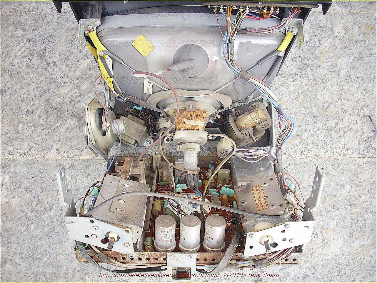
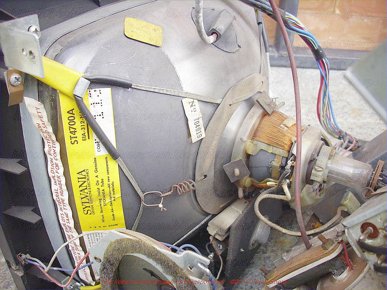
The set has all basic commands above the screen and allows power supply from mains 220v and a 12volt source and is a slightly rare thing.
The set is branded FIDES which was an Italian industry brand name property of the Italian appliances factory / industry IGNIS (known for the IGNIS K563 washing machines and derivatives and the PHILIPS developed P.M. SYSTEM series.)
The set is fabricated by Emerson.
The Original Italian brand conglomerate was formed by IGNIS (Main) FIDES and ALGOR (All dead).
The Ignis was a manufacturer of home appliances. Currently is a trademark owned by the US multinational Whirlpool Corporation.
The milanese entrepreneur
Giovanni Borghi founded in 1946 in Comerio (VA) the SIRI S.p.A., acronym
for Refrigerant Industry Company Ignis. The term
Ignis, which will be the brand name comes from the Latin and means
"flame", and in fact, the company began its activities by building
electric hobs.
During the 1950s the
company grew in terms of productivity, and extend it to gas cookers,
irons, electrical water heaters and refrigerators, the latter also
products for third parties with some brands such as Atlantic, Fiat,
Philco, Phonola and RadioMarelli. At the same time created other establishments, Gavirate, Naples and Cassinetta di Biandronno.
The company, in the 1960s
and 1970s continued its expansion by creating settlements in Siena and
Trento, and also abroad, two in Spain and one in Greece. He also started the production of washing machines, dishwashers and microwaves. Commercially
Ignis was one of the leading companies in the domestic market of home
appliances in 1960, holding a market share of 38%.
In 1970, 50% of the share capital of the company was taken over by Philips, which acquired full control in 1972.
Ignis
was in those years, after the Zanussi, the second national manufacturer
of household appliances, and in 1973 its factories were more than 10000
employees only in Italy.
With
the change of ownership at the Dutch multinational company, he also
changed the corporate name of the company that became IRE S.p.A
(Industrie Riunite Eurodomestici).
In
1988, IRE-Ignis became a joint venture between Philips and Whirlpool,
which entered the capital with 53% of the shares, becoming the majority
shareholder.
The
American company in 1991, acquired the whole of the Ignis, which became
Italy s.r.l, Whirlpool and Whirlpool Europe later, and since then is a
part of the group, which produced household appliances in the Italian
plants, still active (NOT FOR TELEVISIONS !!)
IGNIS, GIOVANNI BORGHI HISTORY.
Investing in the industrial development of artisan villages
in Varese, Italy, Giovanni Borghi builds a factory for 200
employees to manufacture not only ovens and cooktops, but
also an appliance previously unknown in Italy: the refrigerator.
Ignis workers produce appliances for third-party companies
like Fiat, Atlantic, Philco, Emerson and Philips. Borghi builds
the “Villages of Ignis,” with affordable one- and two-family
houses (Borghi Villages), as well as a pool and sports center
in Comerio, Italy, and a hostel vvith recreational facilities for
young workers in Cassinetta, Italy, all intended to promote a
comfortable, healthy lifestyle.
 The Milan industrialist Giovanni Borghi founded
the IGNIS brand of household appliances. His factories would turn out
one appliance every eight seconds, and make billions selling them to
Italy's exploding middle class. Borghi was famous for his early
support of cycling, and his yellow IGNIS jerseyed squadra won more than a
few great races in the late fifties and early sixties.
The Milan industrialist Giovanni Borghi founded
the IGNIS brand of household appliances. His factories would turn out
one appliance every eight seconds, and make billions selling them to
Italy's exploding middle class. Borghi was famous for his early
support of cycling, and his yellow IGNIS jerseyed squadra won more than a
few great races in the late fifties and early sixties.Borghi was aggressive, flamboyant and flashy. And he took care of his stars - famously buying Spanish sprinter Miguel Poblet a Lancia convertible after his Milan San Remo win. On top of his 25 million lire per year salary.
Giovanni
Borghi, was an Italian industrialist pioneer in the field of domestic
appliances, returned from a trip in the USA with a real
illumination: refrigerators insulated with Polyurethane foam were much more
efficient and capacious than those hand-filled with mineral wood.
His refrigerators Group, Ignis, developed internally this technology and the
related equipment, a suitable alternative to the imported foam dispensers, which
were difficult to get, fix and maintain, stimulating an industrial supply of
similar machines.

Borghi kept control of IGNIS in the family. In the paternalistic Italian industrial model - like Ferrari, Maserati or Campagnolo. He later turned the reins over to his son, who in turn finally sold the company to Dutch conglomerate, Philips.
When Philips decided to get into the major household appliances
market, its procedure was to buy increasing quantities of these goods from the Italian firm, Ignis, then at the height of its prosperity.
Once it became the principal client of the manufacturer, it took over supplying the latter by purchasing 50 percent of its capital. It took over the firm completely in 1972, to the satisfaction of the founder of Ignis, Giovanni Borghi.
In
1988, IRE-Ignis became a joint venture between Philips and Whirlpool,
which entered the capital with 53% of the shares, becoming the majority
shareholder.
The American company in 1991, acquired the whole of the Ignis, which became Italy s.r.l, Whirlpool and Whirlpool Europe later, and since then is a part of the group, which produced household appliances in the Italian plants, still active
BORGHI DIED IN 1975.
Borghi is still remembered in Italia. RAI even aired TV miniseries about his life this past year, "Mister Ignis".
More Notes:
^ Giovanni Borghi, su SAN - Archivi d'impresa. URL consultato il 21 dicembre 2017. ^ Sito web del Quirinale: dettaglio decorato.Readings:
V. Notarnicola, Giovanni Borghi, Milano, Longanesi, 1966.G. Spartà, Mister Ignis: Giovanni Borghi nell'Italia del miracolo, Segrate, Mondadori, 2003, ISBN 88-04-51406-X.
Some Links;
Giovanni Borghi, su SAN - Archivi d'impresa.Giovanni Borghi, in Dizionario biografico degli italiani, Roma, Istituto dell'Enciclopedia Italiana.


