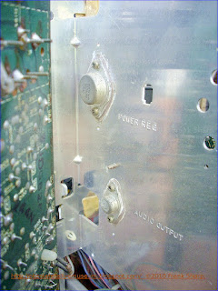
SANYO CTP3203 CHASSIS TP-32030
TAA707AP VIF IC
HA1125 SIF IC
C1025 FRAME OUT
Polarity: NPN
Maximum Collector Power Dissipation (Pc): 25 W
Maximum Collector-Base Voltage Vcb: 120 V
Maximum Collector-Emitter Voltage Vce: 80 V
Maximum Emitter-Base Voltage Veb: 4 V
Maximum Collector Current Ic max: 3 A
Max. Operating Junction Temperature (Tj): 150 °C
Forward Current Transfer Ratio (hFE), MIN: 80
2SC643A HOR OUT (2)
Polarity: NPN
Maximum Collector Power Dissipation (Pc): 50 W
Maximum Collector-Base Voltage Vcb: 1500 V
Maximum Collector-Emitter Voltage Vce: 800 V
Maximum Emitter-Base Voltage Veb: 5 V
Maximum Collector Current Ic max: 2.5 A
Max. Operating Junction Temperature (Tj): 150 °C
Transition Frequency (ft): 1.5 MHz
Collector Capacitance (Cc): 190 pF
Forward Current Transfer Ratio (hFE), MIN: 5
2SC1050 SUPPLY REG OUT
2SD24YK SOUND OUT
2SC1507 RGB AMPL. (3)
Polarity: NPN
Maximum Collector Power Dissipation (Pc): 12 W
Maximum Collector-Base Voltage Vcb: 300 V
Maximum Collector-Emitter Voltage Vce: 250 V
Maximum Emitter-Base Voltage Veb: 6 V
Maximum Collector Current Ic max: 0.25 A
Max. Operating Junction Temperature (Tj): 175 °C
Transition Frequency (ft): 25 MHz
Forward Current Transfer Ratio (hFE), MIN: 60
The electrical components of a television receiver are
assembled in a plurality of modules. Each module is coupled into the set
by means of connectors so that it may be easily removed and replaced if
required. Substantially all of the modules are assembled in a single
chassis in the form of a drawer which can be moved to a forward position
extending outside of the front of the television cabinet for easy
access to each module.
A portion of the electronic modules are pivotally supported on the
chassis so that they may be swung to one side to expose other electronic
modules without removal from the electronic chassis. The connectors
mounted on the electronic chassis have openings in the electronic
chassis positioned adjacent the connectors to provide an area for
soldering the grounding wires to the chassis from the connector. The
opening also prevents contact between the soldering iron and the
connectors to prevent damage to the connectors during the soldering
operation. A power line interlock is provided which disconnects power to
the electronic chassis when the electronic chassis is withdrawn from
the cabinet for maintenance. A connector is provided on the electronic
chassis, accessible from the front of the cabinet with the chassis in
its forward position, to provide means for providing power to the
electronic chassis with the chassis in its forward position.
The electronic modules include a high voltage chassis, a power supply
chassis and a plurality of printed wiring boards with components mounted
thereon. The printed wiring boards are so positioned within the
electronic chassis that they are easily removable and are accessible for
measurements therein without removal from the chassis. The tuners used
within the television receiver are mounted on brackets connected to the
electronic chassis for easy removal of the tuner from the television set
without disassembly of the other components of the electronic chassis.
POWER SUPPLY :a regulated DC power supply circuit comprising a full wave rectification
stage for rectifying an AC input and a regulating stage for regulating
an output voltage from the rectification stage.utilizes a transistor connected in series between a source of
unregulated DC voltage and a load to be supplied with regulated voltage.
This regulated power supply is shown and described in U.S. Pat. No.
3,028,538. An error control voltage is generated in a bridge-like
circuit having a source of reference voltage and a reference resistor as
one branch, the load and a voltage control resistor as a second branch
and the input to a control (error) amplifier as the third branch. The
output of the control amplifier is connected to the control electrode of
the series pass transistor. A power supply unit having a series regulator that changes an input DC
voltage input from a DC power supply into a stabilized output DC voltage
lower than the input DC voltage, includes: a power consuming unit,
provided on a direct current path between the DC power supply and the
series regulator, including a parallel circuit formed by a first fixed
resistor and a semiconductor device.A series regulator (dropper type power supply) is known as a power
supply unit that changes an input direct current (DC) voltage input from
a DC power supply into a stabilized output DC voltage.This series regulator changes the input DC voltage to the stabilized output DC voltage that is lower than the input DC voltage.This
series regulator, however, converts a power loss generated by voltage
drop between an input and an output of a semiconductor device such as a
transistor, used as a three-terminal regulator device serving as a main
controlling device, into heat. Thus, in a case where the voltage drop is
large, the power loss in the semiconductor device also becomes large.
The rectifier output voltage is smoothed in a
smoothing capacitor. Voltage stabilization is provided in the
stabilizing circuits by the use of Zener diode circuits to provide
biasing to control the collector-emitter paths of respective
transistors.A linear regulator circuit according to an embodiment of
the present invention has an input node receiving an unregulated
voltage and an output node providing a regulated voltage. The linear
regulator circuit includes a voltage regulator, a bias circuit, and a
current control device.
In one embodiment, the current
control device is implemented as an NPN bipolar junction transistor
(BJT) having a collector electrode forming the input node of the linear
regulator circuit, an emitter electrode coupled to the input of the
voltage regulator, and a base electrode coupled to the second terminal
of the bias circuit. A first capacitor may be coupled between the input
and reference terminals of the voltage regulator and a second
capacitor may be coupled between the output and reference terminals of
the voltage regulator. The voltage regulator may be implemented as
known to those skilled in the art, such as an LDO or non-LDO 3-terminal
regulator or the like.
The
bias circuit may include a bias device and a current source. The bias
device has a first terminal coupled to the output terminal of the
voltage regulator and a second terminal coupled to the control
electrode of the current control device. The current source has an
input coupled to the first current electrode of the current control
device and an output coupled to the second terminal of the bias device.
A capacitor may be coupled between the first and second terminals of
the bias device.
In the bias device and current source
embodiment, the bias device may be implemented as a Zener diode, one or
more diodes coupled in series, at least one light emitting diode, or
any other bias device which develops sufficient voltage while receiving
current from the current source. The current source may be implemented
with a PNP BJT having its collector electrode coupled to the second
terminal of the bias device, at least one first resistor having a first
end coupled to the emitter electrode of the PNP BJT and a second end, a
Zener diode and a second resistor. The Zener diode has an anode
coupled to the base electrode of the PNP BJT and a cathode coupled to
the second end of the first resistor. The second resistor has a first
end coupled to the anode of the Zener diode and a second end coupled to
the reference terminal of the voltage regulator. A second Zener diode
may be included having an anode coupled to the cathode of the first
Zener diode and a cathode coupled to the first current electrode of the
current control device.
A
circuit is disclosed for improving operation of a linear regulator,
having an input terminal, an output terminal, and a reference terminal.
The circuit includes an input node, a transistor, a bias circuit, and
first and second capacitors. The transistor has a first current
electrode coupled to the input node, a second current electrode for
coupling to the input terminal of the linear regulator, and a control
electrode. The bias circuit has a first terminal for coupling to the
output terminal of the linear regulator and a second terminal coupled
to the control electrode of the transistor. The first capacitor is for
coupling between the input and reference terminals of the linear
regulator, and the second capacitor is for coupling between the output
and reference terminals of the linear regulator. The bias circuit
develops a voltage sufficient to drive the control terminal of the
transistor and to operate the linear regulator. The bias circuit may be
a battery, a bias device and a current source, a floating power
supply, a charge pump, or any combination thereof. The transistor may
be implemented as a BJT or FET or any other suitable current controlled
device.

Power
Supply: The examples chosen are taken from manufacturers' circuit
diagrams and are usually simplified to emphasise the fundamental nature
of the circuit. For each example the particular transistor properties
that are exploited to achieve the desired performance are made clear. As
a rough and ready classification the circuits are arranged in order of
frequency: this part is devoted to circuits used at zero frequency,
field frequency and audio frequencies.
SANYO CTP3203 CHASSIS TP-32030 Chrominance signal gain control circuit
Sanyo Electric Co., Ltd. (JA)
A chrominance signal gain control circuit comprising a band pass amplifier of a gain control type for amplifying a signal including a burst signal and a chrominance signal while the gain thereof is controllable as a function of a control voltage input, a burst amplifier responsive to the output from the band pass amplifier and a burst extra cting pulse, such as a flyback pulse, for extracting and amplifying the burst signal, and an automatic color control detecting circuit responsive to the output from the burst amplifier for providing a peak detected output of the burst signal to the band pass amplifier as a control voltage input, whereby an automatic chrominance signal control is achieved, said circuit further comprising means for providing to the band pass amplifier as another control voltage input a pulse signal having a pulse width and a phase time covering the burst signal, the magnitude of which pulse signal is controllable manually or automatically. Manual adjustment of the magnitude of the pulse signal enables a color saturation control, while automatic adjustment thereof as a function of a color killer voltage enables a color killer operation and automatic adjustment thereof as a function of a peak detected output of the chrominance signal from the band pass amplifier enables a peak color control.
1. A chrominance signal control circuit in a color television apparatus, comprising:
amplifying means of a gain control type for selectively amplifying a composite signal including a burst signal and a chrominance signal, the gain thereof being controllable as a function of a control voltage input,
means for providing a pulse signal having a pulse width and a phase time encompassing the burst signal of said composite signal,
means receiving the selectively amplified composite signal output of said amplifying means and responsive to the pulse signal from said pulse signal providing means for extracting the burst signal from the selectively amplified composite signal,
means for receiving and peak detecting the extracted burst signal and supplying the peak detected burst signal output thereof to said amplifying means as the control voltage input,
means receiving the selectively amplified composite signal output of said amplifying means and providing a peak detected output of the chrominance signal only, of said composite signal, when the peak detected chrominance signal output exceeds a predetermined value, and
means responsive to the burst extracting pulse signal for producing a control pulse output, said means receiving the peak detected chrominance signal output for automatically adjusting the magnitude of the control pulse and supplying the control pulse to said amplifying means for selectively controlling the gain thereof for amplification of the burst signal, thereby to afford peak color control of the selectively amplified, composite signal output of said first amplifying means. .
2. The chrominance signal control circuit in accordance with claim 1, in which said automatic adjusting means is operable as a function of a color disabling voltage, thereby affording color disabling operation.
3. The chrominance signal control circuit as recited in claim 1 wherein said gain control amplifying means comprises:
a first amplifying means receiving the composite signal and responsive to the control pulse output of said means for automatically adjusting the magnitude of the pulse signal, for selectively amplifying the burst signal of the composite signal, and producing an output composite signal having the burst signal thereof selectively amplified, and
second amplifying means receiving the output of said first amplifying means and responsive to the control voltage input thereto, received from said means for providing a peak detected output from said extracted burst signal, for adjusting the gain thereof and correspondingly the amplification of the composite signal output having the selectively amplified burst signal, as produced by said first amplifying means.
4. The chrominance signal control circuit as recited in claim 3 wherein said first amplifying means comprises a video amplifier connected in a stage preceding said second amplifying means.
5. The chrominance signal control circuit as recited in claim 4 wherein said second amplifying means comprises a band pass amplifier.
6. The chrominance signal control circuit as recited in claim 1 wherein said amplifying means has a first input for receiving the composite signal comprising a burst signal and a chrominance signal, and a second input for receiving in common the control pulse for control of the gain thereof for selectively amplifying the burst signal of the composite signal, and the control voltage input for control of the gain thereof for amplification of the composite signal comprising the burst signal and the chrominance signal.
7. A chrominance signal control circuit in a color television apparatus, comprising:
amplifying means of a gain control type for selectively amplifying a composite signal including a burst signal and a chrominance signal, the gain thereof being controllable as a function of a control voltage input, and, selectively, as a function of a control pulse input,
means for providing a pulse signal having a pulse width and a phase time encompassing the burst signal of said composite signal,
means receiving the selectively amplified composite signal output of said amplifying means and responsive to the pulse signal from said pulse signal providing means for extracting the burst signal from the selectively amplified composite signal,
means for receiving and peak detecting the extracted burst signal and supplying the peak detected burst signal output thereof to said amplifying means as the control voltage input,
means receiving the selectively amplified composite signal output of said amplifying mea ns and providing a peak detected output of the chrominance signal only, of said composite signal, when the peak detected chrominance signal output exceeds a predetermined value, and
means responsive to the burst extracting pulse signal for producing a control pulse output having a pulse width and a phase time encompassing the burst signal of said composite signal, and responsive to the peak detected chrominance signal output for automatically adjusting the magnitude of the control pulse output thereof and supplying the control pulse to said amplifying means for selectively controlling the gain of said amplifying means during said phase time encompassing the burst signal of said composite signal, such that an increase of said peak detected chrominance signal output adjusts the magnitude of the control pulse output to increase the gain of said amplifying means for selective amplification of the burst signal, and the control voltage produced in accordance with the peak detected burst signal output reduces the gain of said amplifying means, thereby to afford peak color control of the selectively amplified, composite signal output of said amplifying means.
8. A chrominance signal control circuit in a color television apparatus, comprising:
band pass amplifying means of a gain control type having a first input for receiving the composite signal comprising a burst signal and a chrominance signal, and a second input for receiving both a control voltage and a control pulse input for control of the gain thereof,
means for providing a pulse signal having a pulse width and a phase time encompassing the burst signal of said composite signal,
means receiving the selectively amplified composite signal output of said amplifying means and responsive to the pulse signal from said pulse signal providing means for extracting the burst signal from the selectively amplified composite signal,
means for receiving and peak detecting the extracted burst signal and supplying the peak detected burst signal output thereof to said amplifying means as the control voltage input thereto
means receiving the composite signal output of said amplifying means and providing a peak detected of the chrominance signal only, of said composite signal output, when the peak detected chrominance signal output exceeds a predetermined value, and
means responsive to the burst extracting pulse signal for producing a control pulse output and receiving the peak detected chrominance signal output for automatically adjusting the magnitude of the control pulse output thereof and supplying the control pulse as said control pulse input to said amplifying means for selectively controlling the gain thereof for selective amplification of the burst signal, thereby to afford peak color control of the selectively amplified, composite signal output of said amplifying means.
Description:
BACKGROUND OF THE INVENTION
1. Field of the Invention
The present invention relates to a chrominance signal gain control circuit. More specifically, the present invention relates to an improvement in a manner of controlling the gain of an automatic color control circuit.
2. Description of the Prior Art
FIG. 1 shows a block diagram of a typical prior art automatic color control circuit commonly used in a color television receiver. An intermediate frequency signal is amplitude detected by a detector 9 and the resultant composite video signal is amplified by a video amplifier 10. The composite video signal, as amplified, is applied to a band pass transformer 11, where a chrominance signal as well as a burst signal are extracted. The chrominance signal as well as the burst signal, thus extracted, are applied to a first band pass amplifier 12 and further to a second band pass amplifier 13. A portion of the output from the first band pass amplifier 12 is applied to a burst amplifier 14, where the burst signal is extracted, as a function of a pulse output from pulse source circuit 15, and amplified. The pulse may be a flyback pulse obtainable from a horizontal scan circuit as the circuit 15 or of a delayed horizontal synchronizing pulse obtainable from a synchronization separating circuit as the circuit 15. The burst signal, as extracted and amplified, is applied to an automatic color control detecting circuit (ACC detector) 16 and is amplitude detected thereby. An output from the automatic color control detecting circuit 16 is applied to a control electrode of the first band pass amplifier 12 for control of the gain thereof as a function of the output from the circuit 16. It is to be understood that a closed loop for automatic color control is implemented by the first band pass amplifier 12, the burst amplifier 14, and the automatic color control detecting circuit 16, such that the burst signal output from the band pass amplifier 12 may be of controlled to be constant amplitude in spite of changes in the amplitude of the input signal. FIG. 2 is a graph showing relation between the gain of the first band pass amplifier 12 (ordinate) and the control voltage obtained from the automatic color control detecting circuit 16 (abscissa). As seen from the FIG. 2 graph, such a relation is rather linear.


More detailed description will be made of the operation of automatic color control with particular reference to FIG. 1. As seen from the FIG. 2 graph, the gain control characteristic of the first band pass amplifier 12 is of such a type that a control voltage increasing in a positive going direction as applied to the control electrode of the amplifier 12, increases the gain of the amplifier 12. Now assuming that the input signal to be applied to the first band pass amplifier 12 becomes larger, the output control voltage from the automatic color control detecting circuit 16 becomes lower and accordingly the gain of the amplifier 12 decreases, with the result that the magnitude of the output burst signal from the amplifier 12 is likely to be kept constant.
In general, the amplitude of the chrominance signal may range in magnitude up to a limit that satisfies the following equation: V2 < 2V1
where
V2 is the amplitude of the chrominance signal, and
V1 is the amplitude of the burst signal in the band pass amplifier, as seen in FIG. 3, which shows a wave form of the chrominance signal as well as the burst signal.
However, the ratio of V1 versus V2 varies depending upon the broadcasting stations. Therefore, if the magnitude of the chrominance signal (V2) is controlled in response to the magnitude of the burst signal (V1), a disadvantage will result in practice. More specifically, proper automatic color control could be provided in reception from one broadcasting station, while the chrominance signal could be in a saturated condition in reception from another broadcasting station, although the magnitude of the burst signal has been controlled properly in both cases.
SUMMARY OF THE INVENTION
Briefly described, the present invention is directed to a chrominance signal gain control circuit for the color band pass amplifier in a color television apparatus, such as a color television receiver, wherein a pulse signal having a phase time corresponding to or covering the burst signal is applied to a band pass amplifier to which an automatic color control voltage is applied, or to any other gain control amplifier which may be provided in advance of the band pass amplifier, whereby adjustment of the magnitude of the said pulse signal causes the gain of the amplifier during a burst signal period of time versus the gain of the amplifier during a horizontal scanning period of time, to be controlled relatively to each other, thereby controlling the magnitude of the chrominance signal.
Therefore, a primary object of the present invention is to improve a manner of controlling the gain of an automatic color control circuit in a color television apparatus.
An aspect of the present invention is to manually or automatically control the magnitude of the chrominance signal, in cooperation with a conventional automatic color control circuit by using a pulse signal having a pulse width and a phase time which encompasses the burst signal of the received, composite video signal in a color television apparatus.
These and other objects and features of the present invention will be better understood from the following detailed description of the preferred embodiments when taken in conjunction with the accompanying drawings.
BRIEF DESCRIPTION OF THE DRAWINGS
FIG. 1 shows a block diagram of a typical prior art automatic color control circuit commonly used in a color television apparatus,
FIG. 2 is a graph showing a relation between the gain of the band pass amplifier and the automatic color control voltage,
FIG. 3 shows a wave form of the chrominance signal and the burst signal,
FIG. 4 illustrates a block diagram of an embodiment of a chrominance signal gain control circuit in accordance with the present invention,
FIG. 5 shows a waveform for explanation of operation of the FIG. 4 embodiment,
FIG. 6 shows a block diagram of a preferred embodiment of the present invention, and
FIG. 7 shows a schematic diagram of the FIG. 6 embodiment.
In the figures like reference characters designate like portions.
DESCRIPTION OF THE PREFERRED EMBODIMENTS:
FIG. 4 illustrates a block diagram of a chrominance signal gain control circuit in accordance with the present invention. A significant feature of the present invention is that a burst extracting pulse or a burst sampling pulse is produced and is applied to a control signal input of the first band pass amplifier 12, for example, through a burst extracting pulse control circuit 17, a gain of which is controllable manually or automatically. The remaining portions of the FIG. 4 diagram are substantially the same as those in the FIG. 1 diagram and therefore more detailed description thereof will be omitted.
For the purpose of describing the operation of the FIG. 4 embodiment, first let it b

e assumed that the signal input circuit of the first band pass amplifier 12 is supplied with an input signal as shown in FIG. 5(a). In such a situation, further let it be assumed that the automatic color control circuit is cut off or disabled and the control input circuit of the first band pass amplifier 12 is supplied with a burst extracting pulse, as shown in FIG. 5(b). Then, the gain of the first band pass amplifier 12 increases only during the time period of the burst extracting pulse, so that an output as shown in FIG. 5(c) is obtained at the output of the amplifier 12. Now assume that the automatic color control circuit is properly connected or enabled. Then the automatic color control circuit will operate responsive only to the magnitude of the burst signal (V1), without any regard to the magnitude of the chrominance signal (V2), with the result that the gain of the first band pass amplifier 12 is controlled such that the magnitude of the burst signal (V1) may be kept constant. As a result, the output from the first band pass amplifier 12 becomes V2', as shown in FIG. 5 (d ), which means that the magnitude of the chrominance signal is made to be smaller relatively as compared with the magnitude of the burst signal (V1).
If the gain of the pulse control circuit 17 is adjusted manually, or automatically in response to any suitable control signal as to be more fully described hereinafter, such that the magnitude of the pulse applied to the first band pass amplifier 12 is accordingly controlled, then the magnitude of the chrominance signal is accordingly controlled. If a voltage representative of the presence or absence of the burst signal, e.g. a color killer voltage, is used as the control signal to be applied to the pulse control circuit 17 for automatic adjustment thereof, the pulse control circuit 17 serves to operate as a color killer circuit. On the other hand, a manual adjustment of the pulse control circuit 17 performs substantially the same function as a color saturation adjustment. Conventionally, color saturation adjustment has been made using a variable resistor provided between the first and second band pass amplifiers 12 and 13, which usually makes the circuit concerned complicated. By contrast, color saturation adjustment can be implemented by a simple circuit in accordance with the abovementioned embodiment, inasmuch as the gain of the pulse control circuit 17 can be done in a DC control manner.
As an alternative embodiment, the video amplifier 10 may be an amplifier of a gain control type, a control voltage input of which is supplied with the output from the pulse control circuit 17. For example, the video amplifier 10 may be a gain control amplifier and accordingly the control pulse output of the circuit 17 may in the alternative be applied to the control input electrode of the video amplifier 10 rather than to the input of band pass amplifier 12, as shown by dotted line in FIG. 6, as well as in FIG. 4. In other words, a gain control of only the burst signal for the purpose of the present invention can be done using not only the band pass amplifier 12 of a gain control type but also any amplifier of a gain control type provided in a stage preceding the band pass amplifier 12. It is to be pointed out that the present invention covers such alternative embodiments.
FIG. 6 shows a block diagram of a preferred embodiment of the present invention, wherein the gain of the pulse control circuit 17 is automatically adjusted in response to a different control signal. More specifically, the FIG. 6 embodiment is directed to a peak color control, in which only if and when a peak of the chrominance signal exceeds a predetermined value, the pulse control circuit (pulse magnitude adjust) 17 is enabled to control the first band pass amplifier 12 such that the peak of the chrominance signal may be kept constant. A portion of the output from the first band pass amplifier 12 is applied to peak detector 18, where an output is obtainable only if and when a peak of the chrominance signal exceeds a predetermined value. The output from the peak detector 18 is applied to the control input of the pulse control circuit 17. The other portions of the FIG. 6 embodiment are substantially the same as those in the FIG. 4 embodiment and therefore more detailed description thereof will be omitted.
In operation, when a peak of the chrominance signal exceeds a predetermined value or V2 becomes larger than 2V1, a peak detected output is obtained from the peak detector 18 and is applied to the control input of the pulse control circuit 17 to increase the gain of the circuit 17. In response thereto, the band pass amplifier 12 amplifies the burst signal selectively, as compared with the chrominance signal. On the other hand, the chrominance signal as well as the burst signal will be made smaller through the automatic color control operation of the automatic color control detecting circuit 16. As a result, the chrominance signal is selectively made smaller as compared with the burst signal. Thus a peak color control can be achieved.
A schematic diagram of the FIG. 6 embodiment is shown in FIG. 7, in which the same blocks are denoted by the same reference characters. The first band pass amplifier 12 comprises a differential amplifier comprising transistors TR1 and TR2, and a signal input circuit implemented by a transistor TR3. The chrominance signal input as well as the burst signal input is applied to the base of the transistor TR3 and an output therefrom is applied to the differential amplifier. A control electrode of the transistor TR1 is fixed to a predetermined potential, while a control electrode of the transistor TR2 is supplied with an automatic color control signal from the detecting circuit 16. In accordance with the FIG. 7 embodiment of the present invention, the control electrode of the transistor TR2 is further supplied with the output from the pulse control circuit 17. An output from the first band pass amplifier 12 is taken out through a tank circuit TAK1 and is applied to the second band pass amplifier 13, the burst amplifier 14 and the peak detector 18.
The burst amplifier 14 comprises a transistor TR5 and a tank circuit TAK2 tuned to the frequency of the burst signal. The input electrode of the transistor TR5 is supplied with a chrominance signal as well as a burst signal from the amplifier 12 and a burst extracting pulse from the pulse source 15. The output from the amplifier 14 is applied to the automatic color control detecting circuit 16. The circuit 16 comprise a peak detecting circuit comprising diodes D1 and D2 and an output therefrom is applied to the control input of the first band pass amplifier 12. The pulse control circuit 17 comprises a gain control amplifier comprising a transistor TR4 and the input electrode thereof is supplied with a pulse signal input through a resistor R2 from the pulse source 15 and a control input through a resistor R1 from the peak detector 18.
It is to be understood that the emitter of the transistor TR4 is biased to a predetermin
ed value. Therefore, an output from the peak detector 18 that is of a smaller value is not large enough to enable conduction of the transistor TR4. However, when the output from the detector 18 exceeds a predetermined value, the transistor TR4 is enabled for conduction, so that the circuit 17 provides a pulse output in response to the pulse input signal from the pulse source 15 the pulse having an amplitude in proportion to the output from the detector 18. The pulse output from the circuit 17 is applied to the input electrode of the transistor TR2 of the amplifier 12, which thereby selectively amplifies the burst signal, changing the relative amplitude relationship between the burst and chrominance signals. More specifically, when the pulse output is applied to the base of the transistor TR2, the transistor TR2 becomes more conductive as compared with the transistor TR1, which means that the gain of the amplifier 12 becomes larger only during a burst signal time period. The automatic color control loop, as mentioned previously, then operates to reduce the amplitude of the composite signal in response to the peak detection of the amplified burst signal, through circuits 14 and 16. As a result, peak color control is achieved.
While specific preferred embodiments of the present invention have been described, it will be apparent that obvious variations and modifications of the invention will occur to those of ordinary skill in the art from a consideration of the foregoing description. It is, therefore, desired that the present invention be limited only be the appended claims.
SANYO CTP3203 CHASSIS TP-32030 Vertical deflection circuit
(Sanyo Electric Co., Ltd. (JA) )
In a vertical deflection circuit for use in a television receiver or the like comprising a vertic al oscillation circuit, a saw-tooth wave voltage generating circuit connected to the vertical oscillation circuit and a vertical deflection output circuit to which the output from the sawtooth wave voltage generating circuit is supplied, a capacitance circuit or a clamp circuit is advantageously incorporated in the vertical deflection circuit in order to eliminate bad effects on the interlaced scanning arising from the linearity correction loop.
1. A vertical deflection circuit in which a horizontal signal component synchronized with the horizontal synchronizing signal is applied to a vertical deflection output, said circuit comprising a vertical oscillation circuit for generating a vertical output pulse train in response to vertical synchronizing pulses applied thereto, a saw-tooth wave voltage generator which produces a series of saw-tooth signals in response to said vertical output pulses, a vertical output circuit for amplifying said saw-tooth signals and loading a vertical deflection coil, and a negative current feedback path for vertical linearity correction provided between said vertical output circuit and said saw-tooth wave voltage generator, said saw-tooth wave voltage generator including a switching circuit to be switched in response to said vertical output pulses from said vertical oscillation circuit, a first capacitor for the saw-tooth signal formation wherein said first capacitor is repeatedly charged or discharged in response to said switching circuit and wherein output signals from said vertical output circuit are applied through said negative current feedback path to said first capacitor, and a clamping circuit connected in parallel to said first capacitor for clamping the saw-tooth voltage formed by said first capacitor for a very short period of time including the completion time of the retracing period of said vertical deflection.
2. A vertical deflection circuit as claimed in claim 1, wherein said clamping circuit means comprises a switching element to be rendered conductive for said very short period of time including said completion time of the retracing perio d of said vertical deflection, and a second capacitor for stabilizing said saw-tooth signal which second capacitor is connected in parallel to all or part of said first capacitor when said switching element is rendered conductive.
3. A vertical deflection circuit as claimed in claim 2, wherein said clamping circuit means further includes a resistance which is connected in parallel to said second capacitor and which is adapted, together with said second capacitor, to set the conducting time of said switching element to said very short period of time including said completion time of the retracing period of said vertical deflection.
4. A vertical deflection circuit as claimed in cliam 3, wherein said clamping circuit means further includes a capacitor and a resistance in a series connection to each other and parallel to said second capacitor for preventing the vibration of a picture due to transient phenomenon.
5. A vertical deflection circuit as claimed in claim 2, wherein said clamping circuit means further includes a resistance which is connected in parallel to said switching element, and which is adapted, together with said second capacitor, to set the conducting time of said switching element to said very short period of time including said completion time of the retracing period of said vertical deflection.
6. A vertical deflection circuit as claimed in claim 2, wherein said clamping circuit means further includes a third capacitor connected in parallel to one of the divided resistors connected in parallel to said second capacitor for preventing vibration of picture due to transient phenomenon.
7. A vertical deflection circuit as claimed in claim 1, wherein said clamping circuit means comprises a switching element to be rendered conductive in said very short period of time including said completion time of the retracing period of said vertical deflection and a constant voltage compensator for supplying a constant voltage to said first capacitor when said switching element is rendered conductive.
8. A vertical deflection circuit as claimed in claim 7, wherein said constant voltage compensator for said clamping circuit means comprises a constant voltage source.
9. A vertical deflection circuit as claimed in claim 7, wherein said constant voltage compensator for said clamping circuit means comprises a Zenor diode.
10. A vertical deflection circuit as claimed in claim 7, wherein said switching element and said constant voltage compensator are connected in series to each other and in parallel to said first capacitor for the saw-tooth signal formation.
Description:
The present invention relates to a vertical deflection circuit for use in a television receiver or the like and, more particularly, to a transistorized vertical deflection circuit of a type wherein no vertical output transformer is employed. This type of vertical deflection circuit with no output transformer is generally referred to as an OTL (Output Transformerless) type vertical deflection circuit.
Conventionally, in the known vertical deflection circuit for use in television receivers or the like, various feedbacks are effected to attain good linearity. For example, feedback is effected from a vertical deflection output circuit to a saw-tooth wave voltage generating circuit provided at the stage prior to said vertical deflection output circuit, in which case, when observation is made on the retracing period, a switching transistor for the saw-tooth voltage generating circuit becomes conductive, and horizontal signals from a horizontal deflection circuit and a pincushion correction circuit are in a state liable to be impressed upon the saw-tooth voltage generating circuit through the feedback loop with the vertical scanning being in a different phase relation to the horizontal scanning for each one field. Accordingly, upon completion of the vertical retracing period, voltage across a charge-and-discharge capacitor for the formation of the saw-tooth wave voltage in the saw-tooth wave voltage generating circuit has d.c. level different for each one field, resulting in improper vertical interlaced scanning.
For the purpose of clearly explaining the disadvantages inherent in the conventional vertical deflection circuit of the above described type, the proir art circuit will be described with reference to FIGS. 1 through to 3.
FIG. 1 is a circuit diagram showing the proir art vertical deflection circuit,
FIGS. 2a to 2f are diagrams showing the wave forms of vertical deflection output produced in the prior art vertical deflection circuit of FIG. 1, and
FIG. 3 is a diagram showing the variations of the terminal voltage of a charge-and-dischrge capacitor in the prior art deflection circuit.
Referring to FIG. 1, the circuit arrangement is such that, since a switching transistor 2 for saw-tooth  wave voltage generation whose base is connected to a vertical oscillation circuit 1 is non-conductive in the scanning period, a charge-and-discharge capacitor C1 for forming the saw-tooth wave voltage is gradually charged by a power source +Eb through a resistor 10, while, in the retracing period, as the switching transistor 2 becomes conductive, the charge imparted to the capacitor C1 is discharged through said capacitor C1 with the saw-tooth voltage obtained across the capacitor C1, which sawtooth voltage is subsequently amplified by a driving tansistor 3 and simultaneously inverted to be applied to the bases of the output transistors 4 and 5. More specifically, when the saw-tooth wave voltage Va (at point A in FIG. 1) as shown in FIG. 2a is applied to the base of the driving transistor 3, an amplified and phase-inverted exciting voltage Vb (at point B in FIG. 1) as shown in FIG. 2b appears at the collector of the driving transistor 3 and applied to the bases of the output transistors 4 and 5, so that the output transistor 4 is rendered conductive at the first half of the scanning with a collector current ic1 as shown in FIG. 2c flowing in the collector of the transistor 4, while the output transistor 5 becomes conductive at the latter half of the scanning with a collector current ic2 as shown in FIG. 2d flowing in the collector of the transistor 5. Consequently, a deflection current id as shown in FIG. 2e flows in a vertical deflection coil 6 with voltage Vf as shown in FIG. 2f appearing at a junction P of the emitters of the output transistors 4 and 5.
Accordingly, the feedback loop f including a capacitor 7 and a resistor R1 functions so as to maintain the base potential of the driving transistor 3 alternatingly constant.
When observation is made on the retracing period, the switching transistor 2 is rendered conductive with a current flowing through the charge-and-discharge capacitor C1 in a path shown by a dotted line arrow in FIG. 1, and upon completion of the retracing period, the terminal voltage across the capacitor C1 reaches a certain value.
Since the vertical scanning is in a different phase relation to the horizontal scanning for each one field, there are cases where the terminal voltage across the charge-and-discharge capacitor C1 has different values for each one field due t o the influence of voltages induced in the feedback loop f through a pincushion distortion correction circuit PC and a deflection coil 6, in which case the terminal voltage across the charge-and-discharge capacitor C1 differs in the d.c. level for each one field, resulting in the fluctuation of the d.c. level of the vertical deflection output current and thus deteriorating the interlaced scanning. In other words, the variations of the terminal voltage of the charge-and-discharge capacitor C1 are as shown in FIG. 3 with consequent inferior interlaced scanning, in which FIG. 3 the scanning period is shown by the symbol Ts, the retracing period by the symbol Tr and the horizontal scanning period by the symbol Th.
Accordingly, an essential object of the present invention is to provide a vertical deflection circuit for use in a television receiver or the like in which ill effects of a linearity control feedback loop hindering a proper interlaced scanning are advantageously removed with substantial elimination of the disadvantages inherent in the conventional vertical deflection circuits.
Another important object of the present invention is to provide a vertical deflection circuit of the above described type in which a capacitance circuit is incorporated for substantially increasing the capacity value of a charge-and-discharge capacitor for a predetermined period of time including a retracing period completion time in order to achieve proper and stable interlaced scanning.
A further object of the present invention is to provide a vertical deflection circuit of the above described type in which a clamping circuit comprising a switching element and a constant voltage compensator for supplying a constant voltage to a capacitor for saw-tooth signal formation is provided for improved interlaced scanning.
A still further object of the present invention is to provide a vertical deflection circuit of the above described type which is simple in construction and accurate in functioning with consequent low cost.
According to a preferred embodiment of the present invention, a capacitance circuit is advantageously incorporated in the vertical deflection circuit of FIG. 1, which capacitance circuit further comprises a switching diode connected in series with a resistor and an auxiliary capacitor which are in parallel connection to each other. The capacitor circuit is connected in parallel to the charge-and-discharge capacitor which is connected between the collector of the switching transistor and the feedback loop in the vertical deflection circuit of FIG. 1. The auxiliary capacitor is one having a large capacity as compared with the charge-and-discharge capacitor, while the resistor which is in parallel connection to the auxiliary capacitor is such one as will form, together with the auxiliary capacitor, a large time constant circuit as compared with the vertical deflection period, by which circuit construction the ill effects from the linearity control feedback loop obstructing the proper interlaced scanning are advantageously eliminated.
These and other objects and features of the present invention will become apparent from the following description taken in conjunction with preferred embodiments thereof with reference to the accompanying drawings, in which;
FIG. 4a is a circuit diagram showing one embodiment of a vertical deflection circuit according to the present invention,
FIG. 4b is a similar diagram to FIG. 4a, but vertical deflection output transistors of the same polarity are employed therein,
FIGS. 5 and 6 are diagrams explanatory of the modes of operations of the circuit shown in FIG. 4a,
FIGS. 7 to 9 are circuit diagrams showing modifications of the circuit of FIG. 4a.
FIG. 10 is a circuit diagram showing a second embodiment of a vertical deflection circuit according to the present invention,
FIG. 11 is a circuit diagram showing a third embodiment of a vertical deflection circuit according to the present invention,
FIGS. 12 to 14 are diagrams explanatory of the modes of operations of the circuit in FIG. 11,
FIG. 15 is a circuit diagram showing a modification of the circuit of FIG. 11 and
FIG. 16 is a circuit diagram showing a fourth embodiment of a vertical deflection circuit according to the present invention.
Before the description of the present invention proceeds, it should be noted that like parts are designated by like reference numerals throughout the several views of the accompanying drawings.
Referring now to FIG. 4a, the vertical deflection circuit of the invention includes a vertical oscillation circuit 1 connected to the base of a switching transistor 2 for saw-tooth voltage generation, a charge-and-discharge capacitor C1 for saw-tooth wave voltage formation which is connected at one end thereof to the collector of the switching transistor 2 and to the base of a driving transistor 3 with the other end of the capacitor C1 connected to earth through a peaking resistor R1, two vertical deflection output transistors 4 and 5 of different polarity forming a vertical deflection circuit of a single ended push-pull (SEPP) type, a vertical deflection coil 6 to which a pincushion distortion correction circuit PC, a coupling capacitor 7 and a cancelling voltage supplying capacitor 8 are connected in series with the junction P of the capacitor 8 and the coil 6 connected to a common junction of the vertical deflection output transistors 4 and 5 and with the bases of the transistors 4 and 5 connected at a point B to the output collector of the driving transistor 3 for symmetrically exciting the transistors 4 and 5 by the driving voltage which is the output of the driving transistor 3, and a capacitance circuit 9 directly relevant to the present invention.
It should be noted that instead of the two vertical deflection output transistors 4 and 5 of different polarity to each other described as employed in the embodiment of FIG. 4a, two transistors 4' and 5' of the same polarity may be used with minor alteration in the circuit connection as shown in FIG. 4b, in which case also, the function of the circuit is approximately the same as in the embodiment of FIG. 4a, so that description thereof is abbreviated for brevity. Accordingly, although the description of modifications and other embodiments of the circuit is given hereinafter on the basis of FIG. 4a, it should be construed that these modifications and embodiments are also applicable to the circuit in FIG. 4b.
It should also be noted that, in the above circuit of FIGS. 4a or 4b if the vertical oscillation circuit 1 is formed by a multivibrator type oscillator or by a blocking oscillator, the transistors forming such oscillators may also serve the function of the switching transistor 2 mentioned above.
The above capacitance circuit 9 further includes a switching diode D1 connected in series with a resistor R2 and an auxiliary capacitor C2 which are in parallel connection. The capacitance circuit 9 is connected, between a point A and the feedback loop f of the vertical deflection circuit, in parallel to the charge-and-discharge capacitor C1 which is connected between the collector of the switching transistor 2 and the feedback loop f. The auxiliary capacitor C2 should be one having a large capacity as compared with the charge-and-discharge capacitor C1, while the resistor R2 should be one having a value as will form together with the auxiliary capacitor C2, a large time constant circuit as compared with the vertical deflection period.
In the normally operating condition of the vertical deflection circuit in the embodiment of FIG. 4a, a proper d.c. current appears across the auxiliary capacitor C2 by the time constant circuit comprising the capacitor C2 and the resistor R2 to which feedback current id is applied, and renders switching diode D1 conductive for a very short period of time including the retracing period completion time. In other words, the diode D1 becomes conductive for a very short period of time Δt in FIG. 5, and the circuit in FIG. 4a becomes equivalent to the circuit in which only the capacitor C2 and the resistor R2 are connected in parallel to the capacitor C1. Accordingly, the charge-and-discharge capacitor is substantially composed of the capacity of the above mentioned capacitors C1 and C2 in parallel connection with the capacity value thereof being (C1 + C2) and with the voltage resulting from the undesirable horizontal deflection current which flows into the charge-and-discharge capacitor from the vertical output circuit becoming sufficiently small by the large capacity of the capacitors C1 and C2, thus the ill effects due to the horizontal deflection circuit being remarkably reduced as in FIG. 5 as compared with the case in FIG. 3. In the period other than the above mentioned period Δt, the diode D1 is rendered non-conductive with the circuit in FIG. 4a becoming equivalent to a circuit in which the diode D1 of the capacitance circuit 9 is removed, and consequently with the auxiliary capacitor C2 being irrelevant to the capacitor C1, thus the charging and discharging being effected only by the capacitor C1.
Referring to FIG. 6, the function of the circuit during the very short period of time Δt will be described more specifically hereinbelow. In the prior art circuit in FIG. 1 in which the diode D1, the capacitor C2 and the resistance R2 are not incorporated, voltages at points A and B, and voltage across the resistance R1 (point C) are as shown in FIG. 6. In the circuit of the invention in FIG. 4a having the capacitance circuit 9 comprising the diode D1, the capacitor C2 and the resistance R2, when the potential at the point A is low and the potential at the upper end of the resistance R1 is high, the diode D1 becomes conductive with the capacitor C2 charged, while in the other period, the capacitor C2 is discharged through the resistance R2. In other words, the terminal voltage across the capacitor C2 drops by the discharging amount through the resistance R2 after being charged and the capacitor C2 is subjected to subsequent charging. In the normal operating condition, the discharged amount is equal to the charged amount, so that if the discharging time constant due to the capacitor C2 and the resistance R2 is made sufficiently large as compared with the vertical deflection period, the discharging amount is equivalent to the charging amount during the vertical deflection period by the time constant, and the capacitor C2 is stablized at the charged condition of d.c. potential close to the maximum value of the saw-tooth wave voltage generated at the resistor R1 with the potential thereof slightly fluctuating by the charging and discharging mentioned earlier, which potential is in the direction to bias the diode D1 backward. In other words, in the stationary state, the diode D1 becomes conductive only when the sum of the potential generated at the resistance R1 and the potential at the capacitor C2 is of forward bias, while in the other period, the capacitor C2 is discharged through the resistance R2. If the discharging time constant of the resistance R2 and the capacitor C2 is sufficiently large, the time during which the diode D1 becomes conductive can be made very small as compared with the vertical deflection period.
When the circuit connection of FIG. 4a shown as the first embodiment of the present invention is employed, there are cases where vibrations of pictures are induced due to transient phenomenon during lock in time on synchronization, which undesirable vibrations, however, can be suppressed by the addition of proper phase correction circuits as shown in FIGS. 7 and 8. For such correction circuits, in FIG. 7, a resistor R3 and a third capacitor C3 in series connection are connected in parallel to the time constant circuit comprising the capacitor C2 and the resistor R2 of FIG. 4a.
Referring to FIG. 7, function of the phase correction circuit for preventing the vibrations of pictures due to the transient phenomenon will be more specifically described hereinbelow.
In the conventional vertical oscillation circuits, since the free oscillation frequencies thereof are set at low level as compared with the vertical deflection frequencies, the vertical deflection frequencies carry out deflection at frequencies lower than regular deflection frequences in the channel charge-over etc., so that the saw-tooth wave generating at the resistance R2 becomes larger than that in the normal deflection period with the capacitor C2 charged at high level, in which case, when the deflection frequencies return back to regular level, the capacitor C2 discharges through the resistance R2 and does not function satisfactorily until the potential thereof returns back to the normal level.
In order to overcome the above disadvantages in the prior art circuits, the capacitor C3 and the resis tance R3 are added in the circuit of FIG. 7 of the invention with the capacitor C3 set to be of larger capacity than the capacitor C2 and with the resistance R3 set to be of smaller value than the resistance R2 so that the time constant of the circuit comprising the capacitor C2 and C3 and the resistance R3 is smaller than that of the capacitor C2 and the resistance R2, by which arrangement, the capacitor C2 is charged in the similar manner to the above through the diode D1 with the capacitor C3 charged rather slowly through the resistance R3 and the diode D1. Until the stationary state is reached, a discharging loop through the capacitors C2 and C3 and the resistance R3 is formed, but in the stationary state, the terminal voltages across the capacitors C2 and C3 are approximately equal to each other with the capacitor C2 discharged almost through the resistance R2 and with the capacitor C3 discharged through the resistances R2 and R3. When the capacitors C2 and C3 are steadily working at a normal frequency with the frequency being low for a short period of time and returning back to the normal frequency (low frequency only during the channel change-over period), the saw-tooth wave appearing at the resistance R2 becomes large for a short period of time as earlier mentioned, so that the capacitor C2 is rapidly charged through the diode D1, while the capacitor C3 is charged through the loop via the resistance R3 with consequent slow charging speed. Accordingly, the terminal voltage across the capacitor C3 memorizes the potential at the regular frequency, and when the low frequency returns back to the regular frequency, the charge stored in excess in the capacitor C2 is discharged through the resistance R2 and simultaneously through the resistance R3 and the capacitor C3 so as to rapidly reach the normal level.

In FIG. 8, the resistance R2 of the time constant circuit of FIG. 4a is divided in series into resistances R2 and R3 with a third capacitor C3 connected in parallel to the resistance R3. A similar phase correction circuit to one mentioned above can be connected as shown in FIG. 9, which is another modification of FIG. 4a.
Referring to FIG. 10 showing a second embodiment of the invention, the resistor R1 side of the capacitor 7 is earthed with the feedback loop f connected to point P in FIG. 4a to form a voltage feedback circuit, in which circuit the capacitor C'1 forms a part of the feedback loop f from the vertical deflection output circuit to the saw-tooth wave voltage generating circuit, and also a part of the charge-and-discharge capacity for the formation of the saw-tooth wave voltage with the function thereof being similar to one in FIG. 4a.
Referring now to FIG. 11, there is shown a third embodiment of the invention. In this embodiment, a clamping circuit CL comprising a switching diode D1 and a constant voltage compensator E1 connected in series to each other is connected in parallel to the capacitor C1 for saw-tooth signal formation, which clamping circuit CL is intended to clamp the saw-tooth signal appearing across the capacitor C1 for a very short period of time including the completion time of the retracing period of the vertical deflection. In operation, the switching diode D1 is rendered conductive for the very short period of time including the completion time of the retracing period of the vertical deflection with the constant voltage compensator E1 supplying a constant voltage to the capacitor C1. In other words, the voltage across the charge-and-discharge capacitor C1 is adapted to be clamped at a constant value for a predetermined period of time including the retracing period completion time. In the above circuit arrangement, voltage as shown in FIG. 12 appears across the resistor R1 by the deflection current id flowing through the feedback loop f. It is to be noted that if the switching diode D1 and the constant voltage compensator E1 are not incorporated, voltage as shown in FIG. 13 will appear across the capacitor C1. If the voltage of the constant voltage source is determined to be E1 as shown in FIG. 13, the switching diode D1 becomes conductive in the very small period of time Δt exceeding the voltage E1, so that the voltage across the capcitor C1 is clamped at the voltage E1 for the very small period of time Δt including the retracting period completion time, as shown in FIG. 14, thus the ill effects due to the horizontal deflection circuit are advantageously prevented.
Referring to FIG. 15, there is shown a modification of the embodiment in FIG. 11. In this modification, a Zenor diode Dz is employed instead of the constant voltage compensator E1 in FIG. 11, which Zenor diode Dz connected in series with the switching diode D1 is connected in parallel to the capacitor C1. In this modification, the Zenor diode Dz functions in the similar manner to the constant voltage compensator E1 of the embodiment of FIG. 11.
Referring now to FIG. 16 in which a fourth embodiment of the present invention is shown, a capacitor C'1 is connected in series to a capacitor C1 and in parallel to a constant voltage compensator E1 and a switching diode D1 which are connected in series to each other. In this embodiment, the capacitor C'1 forms a part of the feedback loop f from the vertical deflection output circuit to the saw-tooth wave voltage generating circuit and simultaneously forms a part of the charge-and-discharge capacity for the formation of the saw-tooth wave voltage.
The function of the circuit in FIG. 16 is approximately the same as that of the circuit of FIG. 11, so that description thereof is abbreviated for brevity.
As is clear from the foregoing description, according to the vertical deflection circuit of the invention, the undesirable effects on the vertical interlaced scanning due to the horizontal deflectinon circuit is advantageously prevented through the linearity correction feedback loop, and perfect interlaced scanning can be accurately effected by the simple circuit construction and with the consequent low cost.
Although the present invention has been fully described by way of example with reference to the attached drawings, it is to be noted that various changes and modifications are apparent to those skilled in the art. Therefore, unless otherwise such changes and modifications depart from the scope of the present invention, whey should be construed as included therein.


Osaka portal
Companies portal Kyocera Communications


