Richtige Fernseher haben Röhren!

Richtige Fernseher haben Röhren!

In Brief: On this site you will find pictures and information about some of the electronic, electrical and electrotechnical Obsolete technology relics that the Frank Sharp Private museum has accumulated over the years .
Premise: There are lots of vintage electrical and electronic items that have not survived well or even completely disappeared and forgotten.

Or are not being collected nowadays in proportion to their significance or prevalence in their heyday, this is bad and the main part of the death land. The heavy, ugly sarcophagus; models with few endearing qualities, devices that have some over-riding disadvantage to ownership such as heavy weight,toxicity or inflated value when dismantled, tend to be under-represented by all but the most comprehensive collections and museums. They get relegated to the bottom of the wants list, derided as 'more trouble than they are worth', or just forgotten entirely. As a result, I started to notice gaps in the current representation of the history of electronic and electrical technology to the interested member of the public.

Following this idea around a bit, convinced me that a collection of the peculiar alone could not hope to survive on its own merits, but a museum that gave equal display space to the popular and the unpopular, would bring things to the attention of the average person that he has previously passed by or been shielded from. It's a matter of culture. From this, the Obsolete Technology Tellye Web Museum concept developed and all my other things too. It's an open platform for all electrical Electronic TV technology to have its few, but NOT last, moments of fame in a working, hand-on environment. We'll never own Colossus or Faraday's first transformer, but I can show things that you can't see at the Science Museum, and let you play with things that the Smithsonian can't allow people to touch, because my remit is different.

There was a society once that was the polar opposite of our disposable, junk society. A whole nation was built on the idea of placing quality before quantity in all things. The goal was not “more and newer,” but “better and higher" .This attitude was reflected not only in the manufacturing of material goods, but also in the realms of art and architecture, as well as in the social fabric of everyday life. The goal was for each new cohort of children to stand on a higher level than the preceding cohort: they were to be healthier, stronger, more intelligent, and more vibrant in every way.

The society that prioritized human, social and material quality is a Winner. Truly, it is the high point of all Western civilization. Consequently, its defeat meant the defeat of civilization itself.

Today, the West is headed for the abyss. For the ultimate fate of our disposable society is for that society itself to be disposed of. And this will happen sooner, rather than later.

OLD, but ORIGINAL, Well made, Funny, Not remotely controlled............. and not Made in CHINA.

How to use the site:
- If you landed here via any Search Engine, you will get what you searched for and you can search more using the search this blog feature provided by Google. You can visit more posts scrolling the left blog archive of all posts of the month/year,
or you can click on the main photo-page to start from the main page. Doing so it starts from the most recent post to the older post simple clicking on the Older Post button on the bottom of each page after reading , post after post.

You can even visit all posts, time to time, when reaching the bottom end of each page and click on the Older Post button.

- If you arrived here at the main page via bookmark you can visit all the site scrolling the left blog archive of all posts of the month/year pointing were you want , or more simple You can even visit all blog posts, from newer to older, clicking at the end of each bottom page on the Older Post button.
So you can see all the blog/site content surfing all pages in it.

- The search this blog feature provided by Google is a real search engine. If you're pointing particular things it will search IT for you; or you can place a brand name in the search query at your choice and visit all results page by page. It's useful since the content of the site is very large.

Note that if you don't find what you searched for, try it after a period of time; the site is a never ending job !

Every CRT Television saved let revive knowledge, thoughts, moments of the past life which will never return again.........

Many contemporary "televisions" (more correctly named as displays) would not have this level of staying power, many would ware out or require major services within just five years or less and of course, there is that perennial bug bear of planned obsolescence where components are deliberately designed to fail and, or manufactured with limited edition specificities..... and without considering........picture......sound........quality........
..............The bitterness of poor quality is remembered long after the sweetness of todays funny gadgets low price has faded from memory........ . . . . . .....
Don't forget the past, the end of the world is upon us! Pretty soon it will all turn to dust!

Have big FUN ! !
-----------------------
©2010, 2011, 2012, 2013, 2014 Frank Sharp - You do not have permission to copy photos and words from this blog, and any content may be never used it for auctions or commercial purposes, however feel free to post anything you see here with a courtesy link back, btw a link to the original post here , is mandatory.
All sets and apparates appearing here are property of Engineer Frank Sharp. NOTHING HERE IS FOR SALE !
All posts are presented here for informative, historical and educative purposes as applicable within Fair Use.


Showing posts with label Planet. Show all posts

Sunday, November 4, 2012

NUCLEAR / PLANET (PRANDONI) MOD. 2262 YEAR 1979.


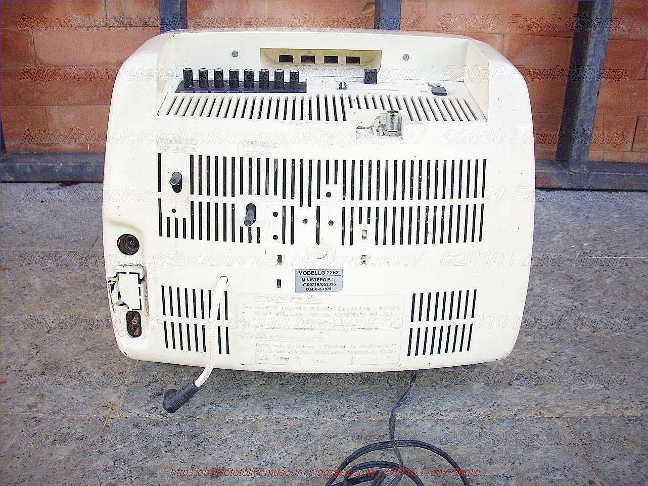
The NUCLEAR / PLANET (PRANDONI) MOD. 2262  is a 12 inches B/W portable television with 8 programs keyboard tuning and potentiometers search system.
The use of voltage-variable diode-capacitors, such as varactor diodes, permits the electronic tuning of radio receivers and television receivers by the use of DC control voltages; so that the tuning elements no longer need to be intimately associated with the tuner. Thus, the tuned circuits of the tv receivers may be located remotely from the devices used to provide the necessary DC tuning voltages. In addition, the compact size of the voltage-variable diode-capacitor tuning circuits makes it desirable to use such tuning circuits in many tv applications which formerly used mechanically adjusted variable capacitors or the like as the tuning elements.

To employ voltage-variable diode capacitors in pushbutton tvs, however, especially in multiband pushbutton tv sets , a problem exists in providing a "memory," so that operation of a pushbutton will provide consistent tuning of the tv receiver to the station which is to be selected by that pushbutton. In addition it is necessary to provide some means for providing the initial tuning of the tv receiver for each pushbutton location in a manner which is reliable and inexpensive.
All commands are above located and the set allows both mains 220volt and 12volt supply types.

Recently, it has become more popular than ever to watch TV in a car as the number of cars increases. In general, a storage battery of 12 volts is used in small cars while one of 24 volts is used in large cars so that there is a disadvantage that a separate power supply device is required for driving a TV set in compliance with the respective battery used in the car. The present invention relates to a power supply circuit of a television receiver used in an automobile, and in particular to a power supply circuit of a television receiver which enables two different voltages from two kinds of supply respectively mains at 220v and dc 12v.

Was marketed with both brand names NUCLEAR and PLANET from PRANDONI Factory in 1979 and was first model with 8 programs tuning keyboard .


In the end of the 60's  increasingly attention was focused on the varicap diode tuner as the latest, sophisticated means of television receiver frontend tuning in both colour and black and white sets.
 The main purpose of this article is to investigate the servicing problems associated with this comparatively new method of tuning.

First however let's briefly recap on the principles involved in this tuning system:

 The tuners use variable capacitance (or "varicap") diodes as the variable tuning elements: the effective capacitance of the diodes is controlled by the reverse bias applied across them, tuning being achieved by varying this voltage. As the reverse bias across a varicap diode is increased so its junction depletion region widens thus reducing its capacitance.

A VHF/ UHF television tuner is constructed in accordance with the present invention includes a preselector tuned circuit having a solid state voltage controlled capacitor as its tunable element, a radio frequency amplifier coupled to the preselector circuit and alsoother circuit to perfect the signal receiving capability and the application the like.

Considering the Mechanical Tuner Problems:

To get the servicing problems in perspective let us next consider the tuning arrangements previously used.
 The earliest of these, employed on v.h.f., was the switched tuner which was either of the turret or incremental type.
 The turret tuner substituted a coil bearing "biscuit" mounted on the rotating drum or turret when channels were changed. Twelve positions were normally provided, with a fine tuning knob to adjust the local oscillator frequency. As its name suggests the incremental tuner simply added more inductance to the tuned circuits at every downward channel movement: thus the highest inductance was present on channel one and the least on channel 12 (which normally covered 13 as well with manipulation of the fine tuner).
The movement towards u.h.f. TV working, initially with dual standard sets and later with single standard ones, brought about the need for u.h.f. tuners. In the earliest u.h.f. receivers valve tuners which were not particularly efficient were used.

The drive mechanism was usually a dual  speed rotary system calibrated from channels 21 to 68. Experience in the field indicated that 625 line television was in many cases considered by the viewer to be inferior to 405 -line reception, on account of the poor signal to noise ratio achieved by the valve tuners. Many viewers were not prepared to use external u.h.f. aerials of course, having achieved satisfactory reception on v.h.f. with an indoor aerial: this aggravated the situation even more.
Another aspect which caused difficulty was the care needed to tune in a u.h.f. channel using a rotary tuner covering the whole of Bands IV and V. Many viewers simply could not tune in BBC 2  or ZDF or ORF or any channel correctly with such a tuning mechanism, finding that they had passed right over the channel they wanted before realising what they had done.
The advent of transistor tuners rapidly improved the quality of u.h.f. reception but use of a rotary mechanism was continued by many manufacturers. Thus while potential reception was improved the same tuning difficulties remained and viewers continued to gravitate towards 405 line viewing using the "old faithful" switched tuner. The operational breakthrough came with the introduction of the push-button u.h.f. channel change. 

The mechanism is basically simple. Adjustable push buttons press down on a lever bar which in turn rotates the tuner's variable capacitors to the appropriate position. Each button is capable of tuning over the entire u.h.f. bands and this leads to customer confusion at times when after some adjustments which were too heavy handed they find themselves receiving ITV on a BBC button or a ORF and ZDF broadcasting or any channel possible !

Mechanical Faults:

 Mechanical tuning obviously has its snags. There are for example contact springs which earth the tuning capacitor and go intermittent. This gives rise to the most random tuning defects, capable of driving the. most patient viewer to a state of total exasperation. It is also possible for the rotation mechanism to hang up and jam intermittently, or just become sticky, so that the reset accuracy of the mechanism is impaired and the receiver has to be retuned every time the channel is changed.

The vanes in the tuning capacitor can also short out at different settings, thereby eliminating some channels. The  Varicap Tuner It will be seen then that mechanical defects can cause very irritating fault symptoms. If one thinks along the lines that anything mechanical is nasty, then the elimination of mechanical parts can only be to the good.

The logic of this is splendid provided the electronic replacement for the mechanical system is more reliable! Otherwise we are leaping out of the frying pan into the fire! In the light of experience gained with mechanical tuning devices it seems great that with the varicap tuner we have at last dispensed with the dreaded rotary tuning capacitor, replacing it instead with a variable voltage to the tuner. 
Let us think about this however since things are never quite as simple as they first appear. The tuning voltage has to be variable in order to tune the receiver. Obviously then a means of varying the voltage has to be provided to act as the tuning control.
As it is a voltage that has to be varied the tuning control takes the form of a potentiometer., Now we have returned to a mechanical system again, though in a less complex form.
A potentiometer is required for each channel, selected by pressing the appropriate channel button.

We have lost a tuning capacitor and its rotating mechanism and gained a set of pots and selector switches therefore. Provided the pots and switches are mechanically more reliable than the tuning capacitor we should be better off-or should we? 

Need for Voltage Stabilisation.
 The voltage selected by the pots cannot be allowed to drift otherwise the receiver will go off -tune. The voltage supply to the potentiometers has to be stabilised therefore and a stabilising zener diode or integrated circuit (TAA550) .is needed for this purpose.

Any failure in this part of the circuit will give rise to tuning drift or worse, a total loss of reception. A short-circuit TAA550 for example will completely remove the tuning voltage while if it is open circuit the tuning can vary with picture brightness. Likewise any intermittency in the potentiometers or associated switching and/or resistors can also cause problems.

Relative Reliability of Tuners:

 It  will be seen then that in order to lose our troublesome mechanical arrangement we have had to introduce considerably more electronics which we trust are going to be more reliable. In addition we have not so far considered the relative reliability of the varicap tuner itself compared with the mechanical type. Since two r.f. transistors are generally used to compensate for the reduced Q of the varicap tuned circuits we immediately have twice the likelihood of an r.f. stage breaking down! 

And being semiconductors the varicap diodes themselves are more likely to fail than the sections of a ganged tuning capacitor. It is reasonable then to conclude that if mechanical faults are the most prevalent the use of varicap tuners will make life easier. Mechanical faults are generally not too difficult to sort out however and the field engineer can often cope with them in the home. 
Can the same be said of the varicap tuner? It seems that this type of tuner does not need so much attention as its mechanical counterpart but is likely to throw up some much more difficult faults when it does, resulting in bench repairs being needed. So far my own experience has indicated that varicap tuning faults nearly always need servicing on the bench.
Generally speaking it seems true to say that varicap tuners themselves are adequately reliable: the snags result from the tuning system and stabilised power supply.

Tuning Drift with Varicap Tuners:

 If a varicap tuned receiver is constantly drifting off tune the +30V supply should be the number one suspect. It is best to connect an Avometer permanently to the supply so that it can be precisely monitored-if necessary write down the exact voltage measured.

 If the receiver drifts, check the voltage. If it has changed, even slightly, this may well be enough to be the cause of the fault. To pinpoint and confirm the diagnosis aerosol freezer should be applied to the stabiliser i.c. or zener. If the voltage returns to normal or changes wildly for the worse the stabiliser is almost certainly the cause of the trouble and should be replaced.
A prolonged soak test should then be carried out. Another point concerning varicap tuners arises with their use in colour receivers.


 There were  makers of the most expensive colour receiver on the market still didn't use a varicap tuner but instead use a mechanical one. The makers' claim is that the signal to-noise ratio of the varicap tuner is inadequate for their colour standards. Undoubtedly the results obtained on the receiver seem to confirm this. Interestingly, the same manufacturers use varicap tuners in their black -and -white receivers, and the tuning button system is often full of troublesome intermittent contacts. The varicap tuner has its advantages and disadvantages then. Probably the simplest comment would be to say that when it is good it is very very good but when it is bad it is horrid!


TRANS CONTINENTS / OCEANIC / PRANDONI was an Italian manufacturer of radio and after of televison sets.

It was also the owner of brands like Trans Continents and Nuclear radio TV or simply Nuclear.

"Prandoni S.p.A." was founded by Dario Prandoni. Finally his son Giorgio Prandoni sold the company to the French "Thomson".

In 1998 Francesco Juilland and Giorgio Prandoni co-founded "Mediacube USA, Inc.", a film production company and a visual effects service provider in USA, Europe and in Italy.
a film production company and a visual effects service provider in USA, Europe and in Italy.

Giorgio Prandoni is a leading figure and heir to the most prestigious industrialist dynasty in the design and manufacture of radio equipment and multi standard television sets in Italy. (His father was Dario Prandoni the luminary owner of Prandoni S.p.A. one of Europe's most highly regarded electronic companies;


Dario Prandoni formed the basis of the Prandoni Empire and Giorgio Prandoni sells the company in France to Thomson with a big one deal). During his tenure from 1998 to February 2002 as Mediacube's CEO Francesco Juilland has created important joint venture between Mediacube USA, Inc. and important European, American and Canadian companies. He also brokered the acquisition of a share of Minerva Pictures (Italy) they own a library of more than 1,500 titles of which 850 are for worldwide rights in perpetuity. The titles include classics works by Pasolini, Germi, Bellocchio, Godard, Fellini, Antonioni and others. Most recently in 2000, Francesco Juilland was elected in the Board of Directors of Ionic WW Studios, a fully digital Hollywood studio organized and financed by Mediacube as Major Investor together with Giorgio Prandoni and Javier Rodriguez, Spanish businessman and scion of an important and conservative Family of Spain full of history and tradition and thank to the greenlight of a guardian angel like the economist Mr. Diego Colombo, chairman of the Colombo Group with offices in Switzerland and around the world and longtime serious advisor of the Juilland family office. Francesco Juilland is in the Board of Directors with the man that he considers his American mentor Mike Medavoy (producer, former chairman of Tristar Pictures and a legendary "Hollywood industry hero" as Fox News channel calls him, many times Oscars winner, his movies including the masterpieces Apocalypse Now, Philadelphia, Dance with wolves, Who flew over the Cuckoo's nest, Annie Hall, Platoon, Rocky, the Sting, Silence of the lambs, Amadeus, The Terminator, Sleepless in Seattle) and Norman Pattiz (called from "USA Today" and "LA Times" The Ted Turner of the radio) and Arnold Messer (president of Phoenix Pictures, company producer of Larry Flint, The thin red line, U-Turn, The 6th Day, Basic, Holes, Stealth, All the King's men), together with David Hayden and Gigi Pritzker (film producer with Deborah del Prete of "the Wedding Planner" with Jennifer Lopez)


Further Readings and Notes

^ Radiogrammofono PDRS 9 (PDF), in Selezione Radio, Anno I, nº 2, Febbraio 1950.
^ Brevetto per marchio d'impresa nr. 05875 del 1 febbraio 1952.
^ Baiocato, NRC 333 Radio Nuclear Radio Corporation; Cassano D'Adda MI,, su www.radiomuseum.org. URL consultato il 16 febbraio 2018.
^ Carlo Grimaldi, Tutto a transitors (PDF), in Informazione industriale, 1967.
^ Guidi, Stereo-Matic Hi-Fi 75 R-Player Prandoni SPA; TREVIGLIO BG, b, su www.radiomuseum.org. URL consultato il 16 febbraio 2018.
^ La Prandoni ritorna in attivo (PDF), in Selezione di tecnica Radio TV, Settembre 1982, p. 6.

External links for further information


NUCLEAR / PLANET (PRANDONI) MOD. 2262 CHASSIS A40-73 INTERNAL VIEW.


All CHASSIS A40-73  parts of the receiver are fitted on one board exept the TUNER and the POWER SUPPLY TRANSFORMER which are on the bottom of the cabinet.

The CHASSIS TECHNOLOGY is based on ASIC'S which are:TCA511 TBA311A17 TBA120SQ TAA611B12 and lots of discretes. Power supply is delivered after rectifiing via Transistor stabiliser. The set can be power supplyed via a 12Volt source in a socket on the rear of the lid.

Power supply is realized with mains transformer and Linear transistorized power supply stabilizer, A DC power supply apparatus includes a rectifier circuit which rectifies an input commercial AC voltage. The rectifier output voltage is smoothed in a smoothing capacitor. Voltage stabilization is provided in the stabilizing circuits by the use of Zener diode circuits to provide biasing to control the collector-emitter paths of respective transistors.A linear regulator circuit according to an embodiment of the present invention has an input node receiving an unregulated voltage and an output node providing a regulated voltage. The linear regulator circuit includes a voltage regulator, a bias circuit, and a current control device.

In one embodiment, the current control device is implemented as an NPN bipolar junction transistor (BJT) having a collector electrode forming the input node of the linear regulator circuit, an emitter electrode coupled to the input of the voltage regulator, and a base electrode coupled to the second terminal of the bias circuit. A first capacitor may be coupled between the input and reference terminals of the voltage regulator and a second capacitor may be coupled between the output and reference terminals of the voltage regulator. The voltage regulator may be implemented as known to those skilled in the art, such as an LDO or non-LDO 3-terminal regulator or the like.
The bias circuit may include a bias device and a current source. The bias device has a first terminal coupled to the output terminal of the voltage regulator and a second terminal coupled to the control electrode of the current control device. The current source has an input coupled to the first current electrode of the current control device and an output coupled to the second terminal of the bias device. A capacitor may be coupled between the first and second terminals of the bias device.
In the bias device and current source embodiment, the bias device may be implemented as a Zener diode, one or more diodes coupled in series, at least one light emitting diode, or any other bias device which develops sufficient voltage while receiving current from the current source. The current source may be implemented with a PNP BJT having its collector electrode coupled to the second terminal of the bias device, at least one first resistor having a first end coupled to the emitter electrode of the PNP BJT and a second end, a Zener diode and a second resistor. The Zener diode has an anode coupled to the base electrode of the PNP BJT and a cathode coupled to the second end of the first resistor. The second resistor has a first end coupled to the anode of the Zener diode and a second end coupled to the reference terminal of the voltage regulator. A second Zener diode may be included having an anode coupled to the cathode of the first Zener diode and a cathode coupled to the first current electrode of the current control device.
A circuit is disclosed for improving operation of a linear regulator, having an input terminal, an output terminal, and a reference terminal. The circuit includes an input node, a transistor, a bias circuit, and first and second capacitors. The transistor has a first current electrode coupled to the input node, a second current electrode for coupling to the input terminal of the linear regulator, and a control electrode. The bias circuit has a first terminal for coupling to the output terminal of the linear regulator and a second terminal coupled to the control electrode of the transistor. The first capacitor is for coupling between the input and reference terminals of the linear regulator, and the second capacitor is for coupling between the output and reference terminals of the linear regulator. The bias circuit develops a voltage sufficient to drive the control terminal of the transistor and to operate the linear regulator. The bias circuit may be a battery, a bias device and a current source, a floating power supply, a charge pump, or any combination thereof. The transistor may be implemented as a BJT or FET or any other suitable current controlled device.


Power Supply: The examples chosen are taken from manufacturers' circuit diagrams and are usually simplified to emphasise the fundamental nature of the circuit. For each example the particular transistor properties that are exploited to achieve the desired performance are made clear. As a rough and ready classification the circuits are arranged in order of frequency: this part is devoted to circuits used at zero frequency, field frequency and audio frequencies. Series Regulator Circuit Portable television receivers are designed to operate from batteries (usually 12V car batteries) and from the a.c. mains. The receiver usually has an 11V supply line, and circuitry is required to ensure that the supply line is at this voltage whether the power source is a battery or the mains. The supply line also needs to have good regulation, i.e. a low output resistance, to ensure that the voltage remains constant in spite of variations in the mean current taken by some of the stages in the receiver. Fig. 1 shows a typical circuit of the power -supply arrangements. The mains transformer and bridge rectifier are designed to deliver about 16V. The battery can be assumed to give just over 12V. Both feed the regulator circuit Trl, Tr2, Tr3, which gives an 11V output and can be regarded as a three -stage direct -coupled amplifier. The first stage Tr 1 is required to give an output current proportional to the difference between two voltages, one being a constant voltage derived from the voltage reference diode D I (which is biased via R3 from the stabilised supply). The second voltage is obtained from a preset potential divider connected across the output of the unit, and is therefore a sample of the output voltage. In effect therefore Tr 1 compares the output voltage of the unit with a fixed voltage and gives an output current proportional to the difference between them. Clearly a field-effect transistor could do this, but the low input resistance of a bipolar transistor is no disadvantage and it can give a current output many times that of a field-effect transistor and is generally preferred therefore. The output current of the first stage is amplified by the two subsequent stages and then becomes the output current of the unit. Clearly therefore Tr2 and Tr3 should be current amplifiers and they normally take the form of emitter followers or common emitter stages (which have the same current gain). By adjusting the preset control we can alter the fraction of the output voltage' applied to the first stage and can thus set the output voltage of the unit at any desired value within a certain range. By making assumptions about the current gain of the transistors we can calculate the degree of regulation obtainable. For example, suppose the gain of Tr2 and Tr3 in cascade is 1,000, and that the current output demanded from the unit changes by 0.1A (for example due to the disconnection of part of the load). The corresponding change in Tr l's collector current is 0.1mA and, if the standing collector current of Tr 1 is 1mA, then its mutual conductance is approximately 4OmA/V and the base voltage must change by 2.5mV to bring about the required change in collector current. If the preset potential divider feeds one half of the output voltage to Tr l's base, then the change in output voltage must be 5mV. Thus an 0.1A change in output current brings about only 5mV change in output voltage: this represents an output resistance of only 0.0552.

TAA611-A12 - Dual BTL power audio amplifier


TCA 511 TV HORIZONTAL AND VERTICAL PROCESSOR

The TCA511 is a silicon monolithic integrated circuit in a 16—lead dual in—line plastic
package. It incorporates the following functions: high stability horizontal oscillator,
horizontal APC circuit with high noise immunity and large pull—in range, high stability
vertical oscillator and sawtooth generator.
lt is intended for driving TV horizontal and vertical transistorized output stages.


APPLICATION INFORMATION

Power Supply
The circuit can work with stabilized supply voltage having a value from 9 to 15 V.
A dropping resistor and a filter capacitor may be used to obtain the suipply from higher
voltages; however, the voltage on pins 3 and 4 must never exceed the maximum
permitted voltage.
Synchronization
Pins 2 and 6 can be DC driven if the reference level of the synchronization pulses is
less than 1 V. With reference levels greater than this value, a coupling capacitor must
be inserted in series with the input, and pins 2

and 6 must be connected to ground
via a resistor.
Vertical Oscillator
The capacitor connected to pin 1 must be selected with regard to the frequency
tolerance, to the thermal stability and to the capacitor's ageing.
The width of the output pulse, to be chosen according to the needs of the output
stages, is defined by the resistor connected between pin 1 and pin 16.
Vertical Output
The vertical output is taken from pin 14, which is a buffered output of the sawtooth
voltage generated at pin 15.
The output current from pin 14 is defined by an internal resistor in the integrated
circuit. if a greater current is needed, a resistor may be connected between pin 14
and pin 3.
The oscillator output pulse is available at pin 15 if the capacitor C9 is not connected. _
This configuration is used for driving output stages in which the sawtooth is generated
by Miller effect.
Horizontal Oscillator
The capacitor connected between pin 10 and ground must be selected with regard
to the frequency tolerance, 1:0 the thermal stability and to the capacit0r’s ageing.
In multistandard receivers, the oscillation frequency may be changed by switching the
value of the capacitor connected to pin 10.


TBA 311 TV SIGNAL PROCESSING CIRCUIT


The TBA311 is a monolithic integrated circuit in a 16-lead clual in-line or quad in—Iine
plastic package. It is intended for use as signal processing circuit for black and
white and colour television sets.
The circuit is designed for receivers equipped with tubes or transistors in the deflection
and video output stages, and with PNP or NPN transistors in the tuner and NPN in
the IF amplifier.
Only signals with the negative modulation can be handled by the circuit. The circuit
is protected against short circuit between video output and GND. The TBA 311 includes:


0 VIDEO PREAMPLIFIER with EIMITTER FOLLOWER OUTPUT
0 GATED AGC for VIDEO» IF AMPLIFIER and TUNER
0 NOISE INVERTER CIRCUIT for GATING AGC and SYNC. PULSE SEPARATOR
o HORIZONTAL SYNC. PIULSE SEPARATOR
0 VERTICAL SYNC. PULSE SEPARATOR
0 BLANKING FACILITY for the VIDEO AMPLIFIER.

All circuits were made by:

SGS is Società Generale Semiconduttori - Aquila Tubi E Semiconduttori (SGS-ATES, "Semiconductor General Society - Tubes and Semiconductors Aquila"), later SGS Microelettronica, a former Italian company now merged into STMicroelectronics
SGS Microelettronica and Thomson Semiconducteurs were both long-established semiconductor companies. SGS Microelettronica originated in 1972 from a previous merger of two companies:
  • ATES (Aquila Tubi e Semiconduttori), a vacuum tube and semiconductor maker headquartered in the Abruzzese city of l'Aquila, who in 1961 changed its name into Azienda Tecnica ed Elettronica del Sud and relocated its manufacturing plant in the outskirts of the Sicilian city of Catania
  • Società Generale Semiconduttori (founded in 1957 by Adriano Olivetti).


The line deflection is using the AU110 A Germanium PNP TRANSISTOR, see below the datasheet:

AU110

Germanium PNP

Category: Germanium Transistor, PNP Transistor, Transistor
MHz: <1 MHz
Amps: 10A
Volts: 160V

Ge PNP Power BJT


V(BR)CEO (V)=160
V(BR)CBO (V)=160
I(C) Abs.(A) Collector Current=10
Absolute Max. Power Diss. (W)=30
I(CBO) Max. (A)=100u
h(FE) Min. Static Current Gain=20
h(FE) Max. Current gain.=90
@I(C) (A) (Test Condition)=1.0
@V(CE) (V) (Test Condition)=2.0
Package=TO-3
Military=N


NUCLEAR / PLANET (PRANDONI) MOD. 2262  CHASSIS A40-73  B-W TELEVISION DIAGRAM AND DEFLECTION CIRCUIT:

A unidirectional conductive device is coupled from a base terminal to a collector terminal of a horizontal deflection output transistor in a television receiver and poled in a direction to prevent the transistor from saturating when it is driven into its conductive state during a portion of each deflection cycle. Biasing means is coupled to the diode to preselect the desired operating voltage of the transistor during its conduction period.


1. In a television receiver, a deflection circuit comprising: 2. A circuit as defined in claim 1 wherein said transformer is an auto-transformer and said second terminal is intermediate said first and 3. In a television receiver, a deflection circuit comprising:
Description:
The present invention relates to transistorized deflection circuits utilized in television receivers.

In present day transistor deflection circuits, for example, those used in the horizontal output stage of a television receiver; the output transistor is normally operated in a switching mode, that is, the transistor is driven into saturation during a trace interval of each deflection cycle and driven out of conduction during the retrace portion of each deflection cycle. By operating the transistor in its saturation region, average power losses are minimized. With saturated operation, however, the accumulation of minority carriers in the base region will effect a continuation in the flow of collector current after the trace interval during the initial portion of the retrace interval while the transistor is being driven into its non-conducting state. In addition to causing this undesirable delay time in turning off the transistor, losses occurring during this period may be localized in small areas commonly referred to as "hot spots." These losses are characterized in being regenerative and tend to cause second breakdown of the device. This effect is explained in greater detail in a paper authored by the present inventor and entitled "Thermal Regeneration in Power Dissipating Elements" which appeared in "The Electronic Engineer" publication in the January 1967 issue. Although operating the horizontal output transistor in its saturated region may reduce the average power dissipated in this device during its conduction interval, it increases the possibility of second breakdown during the turn-off time. With the advent of high voltage (1,500 volts) transistors, it is possible to develop the necessary output energy utilizing one of these transistors which can be operated in a non-saturated mode. The circuit of the present invention insures that the deflection output transistor will not be driven into saturation.

Certain low power transistor switching circuits, such as employed in computer applications, have utilized diodes in conjunction with resistive biasing means coupled between the base and collector terminals to prevent the transistor from saturating and thereby increase the maximum switching frequency of the circuit by reducing the turn-off time of the device.

In the solid state deflection art, however, it is desirable to reduce the turn-off time of the device not to increase the frequency of operation of the circuit, but rather to prevent second breakdown of the device as the relatively large inductive voltage pulse appears during the initial portion of the flyback interval, when current flowing through the deflection winding is interrupted to initiate the retrace portion of each deflection cycle.

The non-saturated operation of the deflection output transistor is achieved in circuits embodying the present invention by automatically holding the collector voltage above the saturation level by shunting excess base drive from the base to emitter junction into the collector circuit. Prior transistor deflection systems employ only the saturated operation of the deflection output device.

Circuits embodying the present invention include a deflection output transistor having a diode coupled between its base and collector terminals and poled to prevent the transistor from being driven into saturation during its conduction period of each deflection cycle.

The invention can be more fully understood by referring to the drawings together with the description below and the accompanying claims.

In the drawings:

FIG. 1 illustrates in block and schematic diagram form, a television receiver including a solid state deflection output stage embodying the present invention;

FIG. 2a is a waveform diagram of the voltage present at the collector terminal 55c of transistor 55 in FIG. 1;

FIG. 2b shows the drive current to terminal A in FIG. 1;

FIG. 2c is a waveform diagram of the current in diode 56 in FIG. 1;

FIG. 2d is a waveform diagram of the base current flowing in transistor 55 of FIG. 1;

FIG. 3 is a schematic diagram of an alternative embodiment of the present invention;

FIG. 4a is a waveform diagram of the voltage appearing at the terminal 366 in FIG. 3;

FIG. 4b is a waveform diagram of the drive current to terminal A in FIG. 3;

FIG. 4c is a waveform diagram of the current in diode 356 in FIG. 3; and

FIG. 4d is a waveform diagram of the base drive current to transistor 355 in FIG. 3.

Referring specifically to FIG. 1, an antenna 10 receives television signals and couples these signals to a tuner 12 which selects the desired radio frequency signals of a predetermined broadcast channel, amplifies these signals, and converts the amplified radio frequency signals to a lower intermediate frequency (I.F.). The tuner 12 is coupled to an I.F. amplifier 14 which amplifies the intermediate frequency signals. The I.F. amplifier 14 is coupled to a video detector 16 which derives video information from the I.F. signals. The video detector 16 is coupled to a video driver stage 18 which amplifies the video signals. The video driver stage 18 is coupled to a video output stage 20, an automatic gain control stage 25 and a synchronizing separator stage 42. An output signal from video driver stage 18 may also be coupled to a sound channel (not shown) to reproduce the audio portion of the transmitted television program. The video output stage 20 couples amplified video information to a control element, such as a cathode 28, of a kinescope 30.

The automatic gain control stage 25 operates in a conventional manner to provide gain control signals which are applied to a radio frequency amplifier included in tuner 12 and to the I.F. amplifier 14. Sync separator 42 separates the synchronization information from the video information and also separates the horizontal synchronizing information for the vertical synchronizing information. The vertical synchronizing pulses derived from sync separator 42 are applied to the vertical deflection system 44 which provides the required deflection current to a vertical deflection winding 43 associated with kinescope 30 by means of the interconnection Y--Y. The horizontal synchronizing pulses from sync separator 42 are applied to an automatic frequency control detector 45 which serves to synchronize a horizontal oscillator 46 with the horizontal synchronizing pulses. The horizontal oscillator stage 46 is coupled to a horizontal driver stage 48 which develops the required drive signal and may be coupled by means of an output transformer in stage 48 (not shown) to a transistorized horizontal output stage 50. The transformer secondary, coupled to terminal A, provides a direct current path for the drive current.

The horizontal output stage 50 includes an output transistor 55 having a base, a collector and an emitter terminal 55b, 55c and 55e, respectively. A resistor 52 and a capacitor 53 are coupled in parallel between the horizontal driver stage 48 and the base terminal 55b of transistor 55.

The output stage includes a unidirectional conductive device such as a diode 56 coupled between the base and collector terminals 55b and 55c of transistor 55. Stage 50 also includes a damper diode 57 coupled across transistor 55, a retrace capacitor 58 coupled across transistor 55 and the series combination of a horizontal deflection winding 59 and an S-shaping capacitor 60 also coupled across transistor 55. Output stage 50 also includes a flyback transformer 61 with a primary winding 61p coupled from a source of operating potential (B+) to the collector terminal 55c of transistor 55. A secondary winding 61s on transformer 61 develops high voltage pulses which are coupled to a high voltage rectifier 63 to provide the ultor voltage for application to a terminal 32 on kinescope 30. Flyback transformer 61 may also include additional windings (not shown) for providing, for example, keying pulses to the AGC stage 25.

The output stage 50 in FIG. 1 is a conventional shunt fed trace driven circuit with the exception of the diode 56 and the bias network including resistor 52 and capacitor 53. Beginning at the center of the trace interval of the deflection cycle, the yoke current is zero and capacitor 60 has a maximum charge. The drive signal applied to the base terminal 55b of transistor 55 turns this device on, thereby completing the conduction path for yoke current which includes capacitor 60, yoke 59 and the collector to emitter current path through transistor 55. During this portion of scan the yoke current is supplied by the charge on capacitor 60 and increases to a maximum value in one direction at which time scan retrace is initiated by driving transistor 55 out of conduction by applying an appropriate signal from the driver stage 48 to the base 55b of transistor 55. During the latter portion of the trace interval when the magnitude of the yoke current is increasing, the output transistor of prior circuits is normally driven into saturation and is in this conduction state at the instant retrace is initiated. During the first portion of retrace, the yoke current is at a maximum and resonates with the retrace capacitor 58 by charging capacitor 58 in a polarity to reverse bias the damper diode 57. As the yoke current decreases to zero, capacitor 58 has a maximum charge impressed upon it; and during the second portion of retrace, the capacitor (58) drives current through the yoke in a reverse direction until it is discharged and the voltage across it reverses sufficiently to forward bias damper diode 57. Diode 57 then conducts during this first portion of trace to complete the current path for yoke current which is, at this instant, at a maximum value in a direction in yoke 59 to charge capacitor 60 and is increasing toward zero. At the mid-point of trace the yoke current has reached zero and the cycle is completed by driving transistor 55 into conduction once again.

Turning now to the operation of the circuitry of FIG. 1 including the present invention, reference is made to the waveform diagrams of FIG. 2. The initial portion of trace is represented in FIG. 2 by the time period between t 0 and t 1 in the figure. It is recalled that during this period damper diode 57 is conducting. The voltage at collector terminal 55c of transistor 55 is represented by the voltage waveform (V c ) in FIG. 2a and is equal to the forward voltage drop across diode 57 which is of the order of -0.7 volts. At some non-critical time before t 1 , the horizontal driver 48 provides a drive current (I A ), as is shown in FIG. 2b. This current flows through diode 56 as is illustrated in FIG. 2c, since the diode is forward biased. [The cathode of diode 56 is at the same voltage as collector terminal 55c (-0.07 volts) and the drive current produces a positive voltage at point A which is at the anode of diode 56.] As time t 1 (the center of trace) is reached, damper diode 57 turns off allowing the collector voltage on transistor 55 to increase as shown in FIG. 2a. At the same time, a portion of the drive current flowing into terminal A is conducted by the now forward biased base to emitter junction of transistor 55 as is illustrated by the waveform of FIG. 2d. Transistor 55 is now conducting the increasing yoke current during the latter portion of scan represented by the period from t 1 to t 2 in FIG. 2. As the magnitude of the yoke current increases during the t 1 to t 2 interval, the base current in transistor 55 increases as shown in FIG. 2d. Diode 56 conducts as illustrated in FIG. 2c to shunt the remaining portion of the applied drive current at terminal A. It is noted that the sum of the currents shown in FIGS. 2c and 2d will equal the current shown in FIG. 2b. The values of resistor 52 and capacitor 53 can be selected to hold the transistor collector voltage at a preselected value sufficient to prevent saturation of the transistor 55. If, for example, the voltage across capacitor 53 is 5.3 volts, the voltage at terminal A with respect to ground will be approximately 6 volts (5.3 volts plus the forward voltage drop across the base-emitter junction of transistor 55). The collector voltage will then be approximately equal to the voltage at terminal A less the forward voltage drop across diode 56. It is desirable to choose values of resistor 52 and capacitor 53 to operate transistor 55 near but not into the saturation region of conduction during the latter portion of each trace interval.

At time t 2 retrace is initiated by applying a relatively large negative drive signal as shown in FIG. 2b to the base terminal of transistor 55. During the retrace interval (t 2 to t 0 in FIG. 2), the collector voltage increases in a typical manner as illustrated in FIG. 2a. At time t 0 the cycle is again repeated.

The circuit modification illustrated in FIG. 3 is another embodiment of the invention which reduces the change in voltage applied to the yoke 59 of FIG. 1 at time t 1 . As shown in FIG. 2a, when diode 57 turns off and transistor 55 conducts, the voltage at the collector terminal 55c of transistor 55 changes by as much, for example, as 6 volts. This voltage change, which is coupled to the yoke 59, will vary the rate of change of yoke current during the center of trace and may, in certain circuits, cause an undesirable non-linearity in the scanning rate. As FIG. 4a illustrates, the circuit of FIG. 3 reduces this change in voltage at the mid-point of trace (t 1 ).

Referring to FIG. 3, the circuit elements which correspond to those of FIG. 1 are prefaced by the numeral 3. In explaining FIG. 3, it is helpful to refer to the waveform diagrams of FIG. 4. Transformer 364 in FIG. 3 is a tightly coupled auto-transformer wherein the tap point 365 may be, for example, at the 5 percent point on the transformer. That is, the segment between terminals 365 and 366 contain 5 percent of the total number of windings on transformer 364. Transformer 364 may also include a secondary winding such as the high voltage winding which is not shown in the figure. In operation, as drive current is applied at sometime prior to t 1 as is shown in FIG. 4b, damper diode 357 is conducting and the voltage at terminal 366 is therefore at approximately -0.7 volts. Drive current flowing into terminal A as represented in FIG. 4b will be conducted by diode 356 during this interval as indicated by the diode current waveform in FIG. 4c. At the middle portion of trace (t 1 ), the damper diode turns off and voltage at terminal 366 is thereby allowed to go slightly positive (less than 0.7 volts). The collector voltage of transistor 355 is held at a value of approximately 5 volts (assuming, for example, the B+ voltage is equal to 100 volts and the collector is coupled to the tap 365 on transformer 364 at a 5 percent point). At this instant, the base to emitter junction will be forward biased and transistor 355 conducts. It is seen that the anode voltage of diode 356 is at approximately +0.7 volts and its cathode which is coupled to terminal 366 is at a less positive voltage. Diode 356 begins to conduct during the latter portion of trace as illustrated by the current waveform diagram shown in FIG. 4c.

During the latter portion of trace, the transistor tends to saturate and the collector voltage at terminal 355c tends to decrease. As this occurs, more current will flow from the B+ terminal through the upper portion of transformer 364. Due to the relatively tight coupling of the segments of transformer 364, terminal 366 experiences a decrease in voltage which controls the forward bias applied to diode 356 to shunt sufficient drive current to hold the transistor 355 out of saturation. The collector voltage of transistor 355 is thus held at some preselected value depending on the location of tap point 365 on transformer 364. Since transformer 364 is utilized, terminal 366 will remain at a low voltage during the latter portion of trace as shown in FIG. 4a, and diode 356 will be forward biased during the application of a positive drive signal to terminal A. As before, the base drive current will increase and diode 356 conduction will decrease generally as shown in FIGS. 4c and 4d during the latter portion of trace. At time t 2 in FIG. 4, a negative drive pulse is applied to the circuit which initiates the retrace interval of the deflection cycle.

Although the specific embodiments of the invention are illustrated in the horizontal deflection output stage of a black and white television receiver, the invention has equal applicability to other deflection systems and may be utilized in a color television receiver.


GENERAL BASIC TRANSISTOR LINE OUTPUT STAGE OPERATION:

The basic essentials of a transistor line output stage are shown in Fig. 1(a). They comprise: a line output transformer which provides the d.c. feed to the line output transistor and serves mainly to generate the high -voltage pulse from which the e.h.t. is derived, and also in practice other supplies for various sections of the receiver; the line output transistor and its parallel efficiency diode which form a bidirectional switch; a tuning capacitor which resonates with the line output transformer primary winding and the scan coils to determine the flyback time; and the scan coils, with a series capacitor which provides a d.c. block and also serves to provide slight integration of the deflection current to compensate for the scan distortion that would otherwise be present due to the use of flat screen, wide deflection angle c.r.t.s. This basic circuit is widely used in small -screen portable receivers with little elaboration - some use a pnp output transistor however, with its collector connected to chassis.

Circuit Variations:
Variations to the basic circuit commonly found include: transposition of the scan coils and the correction capacitor; connection of the line output transformer primary winding and its e.h.t. overwinding in series; connection of the deflection components to a tap on the transformer to obtain correct matching of the components and conditions in the stage; use of a boost diode which operates in identical manner to the arrangement used in valve line output stages, thereby increasing the effective supply to the stage; omission of the efficiency diode where the stage is operated from an h.t. line, the collector -base junction of the line output transistor then providing the efficiency diode action without, in doing so, producing scan distortion; addition of inductors to provide linearity and width adjustment; use of a pair of series -connected line output transistors in some large -screen colour chassis; and in colour sets the addition of line convergence circuitry which is normally connected in series between the line scan coils and chassis. These variations on the basic circuit do not alter the basic mode of operation however.

Resonance
The most important fact to appreciate about the circuit is that when the transistor and diode are cut off during the flyback period - when the beam is being rapidly returned from the right-hand side of the screen to the left-hand side the tuning capacitor together with the scan coils and the primary winding of the line output transformer form a parallel resonant circuit: the equivalent circuit is shown in Fig. 1(b). The line output transformer primary winding and the tuning capacitor as drawn in Fig. 1(a) may look like a series tuned circuit, but from the signal point of view the end of the transformer primary winding connected to the power supply is earthy, giving the equivalent arrangement shown in Fig. 1(b).

The Flyback Period:
Since the operation of the circuit depends mainly upon what happens during the line flyback period, the simplest point at which to break into the scanning cycle is at the end of the forward scan, i.e. with the beam deflected to the right-hand side of the screen, see Fig. 2. At this point the line output transistor is suddenly switched off by the squarewave drive applied to its base. Prior to this action a linearly increasing current has been flowing in the line output transformer primary winding and the scan coils, and as a result magnetic fields have been built up around these components. When the transistor is switched off these fields collapse, maintaining a flow of current which rapidly decays to zero and returns the beam to the centre of the screen. This flow of current charges the tuning capacitor, and the voltage at A rises to a high positive value - of the order of 1- 2k V in large -screen sets, 200V in the case of mains/battery portable sets. The energy in the circuit is now stored in the tuning capacitor which next discharges, reversing the flow of current in the circuit with the result that the beam is rapidly deflected to the left-hand side of the screen - see Fig. 3. When the tuning capacitor has discharged, the voltage at A has fallen to zero and the circuit energy is once more stored in the form of magnetic fields around the inductive components. One half -cycle of oscillation has occurred, and the flyback is complete.

Energy Recovery:
First Part of Forward Scan The circuit then tries to continue the cycle of oscillation, i.e. the magnetic fields again collapse, maintaining a current flow which this time would charge the tuning capacitor negatively (upper plate). When the voltage at A reaches about -0.6V however the efficiency diode becomes forward biased and switches on. This damps the circuit, preventing further oscillation, but the magnetic fields continue to collapse and in doing so produce a linearly decaying current flow which provides the first part of the forward scan, the beam returning towards the centre of the screen - see Fig. 4. The diode shorts out the tuning capacitor but the scan correction capacitor charges during this period, its right-hand plate becoming positive with respect to its left-hand plate, i.e. point A. Completion of Forward Scan When the current falls to zero, the diode will switch off. Shortly before this state of affairs is reached however the transistor is switched on. In practice this is usually about a third of the way through the scan. The squarewave applied to its base drives it rapidly to saturation, clamping the voltage at point A at a small positive value - the collector emitter saturation voltage of the transistor. Current now flows via the transistor and the primary winding of the line output transformer, the scan correction capacitor discharges, and the resultant flow of current in the line scan coils drives the beam to the right-hand side of the screen see Fig. 5.

Efficiency:
The transistor is then cut off again, to give the flyback, and the cycle of events recurs. The efficiency of the circuit is high since there is negligible resistance present. Energy is fed into the circuit in the form of the magnetic fields that build up when the output transistor is switched on. This action connects the line output transformer primary winding across the supply, and as a result a linearly increasing current flows through it. Since the width is
dependent on the supply voltage, this must be stabilised.

Harmonic Tuning:
There is another oscillatory action in the circuit during the flyback period. The considerable leakage inductance between the primary and the e.h.t. windings of the line output transformer, and the appreciable self -capacitance present, form a tuned circuit which is shocked into oscillation by the flyback pulse. Unless this oscillation is controlled, it will continue into and modulate the scan. The technique used to overcome this effect is to tune the leakage inductance and the associated capacitance to an odd harmonic of the line flyback oscillation frequency. By doing this the oscillatory actions present at the beginning of the scan cancel. Either third or fifth harmonic tuning is used. Third harmonic tuning also has the effect of increasing the amplitude of the e.h.t. pulse, and is generally used where a half -wave e.h.t. rectifier is employed. Fifth harmonic tuning results in a flat-topped e.h.t. pulse, giving improved e.h.t. regulation, and is generally used where an e.h.t. tripler is employed to produce the e.h.t. The tuning is mainly built into the line output transformer, though an external variable inductance is commonly found in colour chassis so that the tuning can be adjusted. With a following post I will go into the subject of modern TV line timebases in greater detail with other models and technology shown here at  Obsolete Technology Tellye !


- The EHT Output is realized with a selenium rectifier.

The EHT selenium rectifier which is a Specially designed selenium rectifiers were once widely used as EHT rectifiers in television sets and photocopiers. A layer of selenium was applied to a sheet of soft iron foil, and thousands of tiny discs (typically 2mm diameter) were punched out of this and assembled as "stacks" inside ceramic tubes. Rectifiers capable of supplying tens of thousands of volts could be made this way. Their internal resistance was extremely high, but most EHT applications only required a few hundred microamps at most, so this was not normally an issue. With the development of inexpensive high voltage silicon rectifiers, this technology has fallen into disuse.A selenium rectifier is a type of metal rectifier, invented in 1933. They were used to replace vacuum tube rectifiers in power supplies for electronic equipment, and in high current battery charger applications.

The photoelectric and rectifying properties of selenium were observed by C. E. Fitts around 1886 but practical rectifier devices were not manufactured routinely until the 1930s. Compared with the earlier copper oxide rectifier, the selenium cell could withstand higher voltage but at a lower current capacity per unit area.

NUCLEAR / PLANET (PRANDONI) MOD. 2262 CHASSIS A40-73 CRT TUBE 12".


A RUSSIAN CRT TUBE !


Wednesday, June 6, 2012

PLANET MOD. 602 YEAR 1970.


The PLANET MOD. 602 is a wooden cabinet 19 inches B/W television with 4 programs mechanic keyboard tuning system...............tubes based tv........................ and semiconductors tuner unit developed.

This invention relates to a keyboard for presetting the tuning of a television receiver receiving apparatus, comprising a tuning setting member manually operable for setting up the tuning for the reception of a plurality of transmitters and a group of depressible keys. More particularly, the invention relates to a keyboard for a television receiver receiving apparatus to be used at home domestically, known as television receiver, wherein each key is associated with a tuning storing element adapted to cooperate with the setting member in such a manner that in a first condition of the key said element is conditioned to store the tuning preset by said member and in a second condition of the key the element automatically sets up said member according to the stored tuning.
The main object of the invention is to provide a keyboard for a television receiver receiving apparatus, wherein the tuning setting member cooperates directly with the tuning storing element, whereby the tuning is memorized with a very high precision, while requiring a reduced space. To this end, according to the invention, each tuning storing element includes a wedge pivotally mounted with respect to the associated key, the tuning setting member being provided, in correspondence with each one of said elements, with a pair of converging tapered profiles adapted to cooperate directly with the associated wedge.  Such keyboards for radio and television sets are per se known. They comprise keys of variable lengths, fitted with cams, which can be locked in position, each position corresponding to the tuning of the receiver to a given frequency, and control means, which, upon the actuation of one of the keys, transmit this position to the tuning circuit of the receiver. However, the known keyboards of this type occupy a considerable space, which forms a disadvantage where, as it is the case with motorcar dashboards, space is at a premium and therefore the opening or receptacle allotted for the installation of the receiver therein is of necessity small.

Incorporated antennas for both VHF UHF channels are fitted rear side.

Chassis was hybrid TUBES type even with a full steel chassis structure.


The B/W Tubes Television set was powered with a External Voltage stabiliser unit (portable metal box) which relates to voltage regulators of the type employed to supply alternating current and a constant voltage to a load circuit from a source in which the line voltage varies. Such regulators are frequently provided employing saturable core reactors and condensers connected in circuit...  in such manner as to provide a plurality of variable voltage vectors which vary in different senses, as the line voltage varies, but which add vectorially in such manner that their vector sum remains substantially constant upon variations in line voltage, for providing automatic voltage stabilization of single or multiphase A. C. circuits where the supply voltage and frequency are subject to variation above and below normal value and where the load is subject to variation between normal limits.
voltage stabilization
is automatically effected by the provision of an inductive pilot control device which is adapted to provide two excitation supply voltages for producing excitation or satuation of two magnetic circuits of a reversible booster transformer unit or units and diversion of flux from one magnetic circuit to the other, the booster unit being energized by primary windings from the A. C. supplysystem and being provided with a secondary winding or windings connected between the supply system and the corresponding inain or distribution circuit and in series therewith, through which a corrective boost voltage is
imrorjiiced into the circuit under the influence of the pilot control device, of an amount equal to that of the supply voltage fluctuation which initiated it and appropriate in polarity and direction for restoring the voltage to normal value and providing automatic stabilization of the circuit voltage against supply voltages which fluctuate above and below normal value.

The pilot control device which may be employed singly or may comprise three units or their equivalent when applied to multiphase supply systems comprises a pair of closed magnetic circuits or cores constructed of strip wound magnetic material or stacked laminations, the two
circuits forming a pair being constructed of materials possessing dis~similar magnetic characteristics when jointly energized by identical windings in series or by a collective primary winding, the said magnetic circuits being suitably proportioned to provide equal fluxes when ener-
gized at normal voltage.

The pilot control device is provided with a main and an auxiliary secondary winding or group of windings, the main secondary winding or windings being adapted to provide a voltage representing the difference in the fluxes of the two circuits to which it is jointly associated, while
the auxiliary secondary winding embraces only one circuit, preferably that subject to the least amount of flux variation. Either of the windings consists of two equal sections or in effect a double winding with a center tapping to which one end of the single winding is connected.

The voltage in the single secondary winding of the pilot device becomes directionally additive to that in one half of the tapped secondary winding and substractive in respect to that in the other half. When the supply voltage is normal the voltage provided by the single secondary winding is zero, since there is no difference of flux in the two magnetic circuits, and the two excitation voltages
produced in the halves of the other secondary winding are equal and when connected to the two excitation windings of the booster units, do not produce any diversion of flux between the two circuits or sets of circuits in the magnetic system of the booster transformer unit become equal, and since the series winding on the booster unit is arranged to provide a voltage due to the difference of
the fluxes in its two magnetic circuits or sets of magnetic circuits, no corrective voltage is introduced into the main circuit by the booster. If, however, the supply voltage varies from normal the pilot control device provides a voltage across the one secondary winding due to the difference in the fluxes of the two dis-similar magnetic circuits of which it is comprised, which voltage is combined with thosc in the halves of the other secondary winding to provide two excitation voltages which vary complementarily to each other as the supply voltage fluotuates, and cause a transference of flux between the two
circuits or groups of circuits in the booster unit and automatically provide a corrective boost voltage in the main circuit in which the series winding of the booster transformer is includcd of a value equal to that of the variation in supply voltage which initiated it.
The pilot device may be arranged in various ways, forboth single phase and multiphase operation, as exemplified by the constructions hereinafter more fully described.Similarly, numerous arrangements of the booster transformer unit are possible, some of which are hereinafter described in detail. The booster transformer unit embodies thc principles of the inductive devices described in my co-pending Application No. 411,189, filed February 18, 1954.

As an alternative to the provision of an auxiliary secondary winding on the pilot control device this may be
replaced by an independent or external source of supply,which may be either subject to or independent of supply voltage variation, provided such supply may be arranged with a center tapping if required.

Feed-back arrangements may be employed for providing compensation against voltage drop due to the effects of load in various ways. These are preferably providedon the booster transformer unit and may comprise a current transformer in one or more lines of the main circuit,
the secondary output of the transformer being rectified and arranged to energize an additional excitation winding on the booster transformer unit which in clfect increases the amount of the corrective boost voltage as the load increases.

TRANS CONTINENTS / OCEANIC / PRANDONI was an Italian manufacturer of radio and after of televison sets.

It was also the owner of brands like Trans Continents and Nuclear radio TV or simply Nuclear.

"Prandoni S.p.A." was founded by Dario Prandoni. Finally his son Giorgio Prandoni sold the company to the French "Thomson".

In 1998 Francesco Juilland and Giorgio Prandoni co-founded "Mediacube USA, Inc.", a film production company and a visual effects service provider in USA, Europe and in Italy.
a film production company and a visual effects service provider in USA, Europe and in Italy.

Giorgio Prandoni is a leading figure and heir to the most prestigious industrialist dynasty in the design and manufacture of radio equipment and multi standard television sets in Italy. (His father was Dario Prandoni the luminary owner of Prandoni S.p.A. one of Europe's most highly regarded electronic companies;


Dario Prandoni formed the basis of the Prandoni Empire and Giorgio Prandoni sells the company in France to Thomson with a big one deal). During his tenure from 1998 to February 2002 as Mediacube's CEO Francesco Juilland has created important joint venture between Mediacube USA, Inc. and important European, American and Canadian companies. He also brokered the acquisition of a share of Minerva Pictures (Italy) they own a library of more than 1,500 titles of which 850 are for worldwide rights in perpetuity. The titles include classics works by Pasolini, Germi, Bellocchio, Godard, Fellini, Antonioni and others. Most recently in 2000, Francesco Juilland was elected in the Board of Directors of Ionic WW Studios, a fully digital Hollywood studio organized and financed by Mediacube as Major Investor together with Giorgio Prandoni and Javier Rodriguez, Spanish businessman and scion of an important and conservative Family of Spain full of history and tradition and thank to the greenlight of a guardian angel like the economist Mr. Diego Colombo, chairman of the Colombo Group with offices in Switzerland and around the world and longtime serious advisor of the Juilland family office. Francesco Juilland is in the Board of Directors with the man that he considers his American mentor Mike Medavoy (producer, former chairman of Tristar Pictures and a legendary "Hollywood industry hero" as Fox News channel calls him, many times Oscars winner, his movies including the masterpieces Apocalypse Now, Philadelphia, Dance with wolves, Who flew over the Cuckoo's nest, Annie Hall, Platoon, Rocky, the Sting, Silence of the lambs, Amadeus, The Terminator, Sleepless in Seattle) and Norman Pattiz (called from "USA Today" and "LA Times" The Ted Turner of the radio) and Arnold Messer (president of Phoenix Pictures, company producer of Larry Flint, The thin red line, U-Turn, The 6th Day, Basic, Holes, Stealth, All the King's men), together with David Hayden and Gigi Pritzker (film producer with Deborah del Prete of "the Wedding Planner" with Jennifer Lopez)


Further Readings and Notes

^ Radiogrammofono PDRS 9 (PDF), in Selezione Radio, Anno I, nº 2, Febbraio 1950.
^ Brevetto per marchio d'impresa nr. 05875 del 1 febbraio 1952.
^ Baiocato, NRC 333 Radio Nuclear Radio Corporation; Cassano D'Adda MI,, su www.radiomuseum.org. URL consultato il 16 febbraio 2018.
^ Carlo Grimaldi, Tutto a transitors (PDF), in Informazione industriale, 1967.
^ Guidi, Stereo-Matic Hi-Fi 75 R-Player Prandoni SPA; TREVIGLIO BG, b, su www.radiomuseum.org. URL consultato il 16 febbraio 2018.
^ La Prandoni ritorna in attivo (PDF), in Selezione di tecnica Radio TV, Settembre 1982, p. 6.

External links for further information