


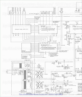
The GRUNDIG SUPER COLOR Einschub W8272 IT CHASSIS 29301-114.63 is a Semi modular chassis.
GRUNDIG SUPER COLOR Einschub W8272 IT CHASSIS 29301-114.63 First GRUNDIG with isolated Chassis from Mains, this because of isolations requirements for featuring external connectivity with VCR and audio devices.
This CHASSIS don't shares much with previous models. Line deflection stages and signal stages and other parts are differently designed and developed even if they're a classic Technology type design or that era employing Thyristor devices.
It introduces the " Stations Computer " as named GRUNDIG Synthesizer tuning system, which is a HIGLY sophisticated circuitry dedicated only to feature Frequency Synthesizer Tuning with OSD Diplaying channels.
This is realized on a separated chassis fitted on the bottom of the cabinet (see Photo)
On the same chassis is fitted the Tuner which is a special in this case type.
The circuit is based on a SIEMENS SDA100 ASICs the SM564 and S047 and other circuits.
All these are NOT Ucontroller or Microprocessor based but special ICs designed for the scope.
Furthermore it eliminates the "battery backup" this because the tuning channels are stored to EAROM Memory type which was power needless.
Furthermore it has even a Time Clock feature even this with OSD on screen display clock which can be called via remote control TELEPILOT 160E.
This is realized with a special ASIC from texas Instruments.
The chassis like other GRUNDIG type has the diagnose socket to obtain quick fault search diagnose process during service.
GRUNDIG SUPER COLOR Einschub W8272 IT CHASSIS 29301-114.63 Frequency synthesizer tuning system for television receivers:(SM564 - SDA100)
GRUNDIG Stations Computer Theory:

A television tuning system employs a frequency synthesizer system for establishing the tuning of the receiver. A programmable frequency divider, controlled by a reversible counter, is connected between the output of a reference oscillator and a phase comparator to which the output of the local oscillator in the tuner also is applied. The phase comparator output provides a tuning voltage for controlling the tuning of the local oscillator. A logic circuit is coupled to sense predetermined relationships of signals from a picture carrier detector, a sound carrier detector, an AFT signal, and the presence of vertical synchronization signal components for changing the count in the reversible binary counter to adjust the programmable frequency divider to compensate for channel frequency offsets which may occur in excess of the pull-in range of the AFT circuit.
As improvements continually have been made in television receivers, the number of adjustments which must be made by the viewer have been substantially reduced. One adjustment, however, which still remains in most receivers is a fine tuning adjustment. Such an adjustment is required even with receivers having automatic fine tuning (AFT or AFC) systems in them. With respect to the VHF channels, the fine tuning adjustment generally is made only when the receiver is first put into operation and then infrequently afterwards as components of the receiver age. For UHF channels, however, a fine tuning adjustment generally is required each time the UHF station is tuned in by the viewer. This is annoying and it is desirable to eliminate the need to such a fine tuning adjustment.
Copending application Ser. No. 537,692, filed Dec. 31, 1974, now U.S. Pat. No. 3,949,158, issued Apr. 6, 1976, is directed to a wide band AFT system which utilizes digital logic circuitry to extend the automatic control range of an AFT system by as much as ±2 megahertz. Such a system substantially minimizes, and in many cases eliminates, the need for fine tuning adjustments of television receivers which are rough-tuned by conventional detent-type turret tuners and the like.
 It is desirable to employ channel selection systems in television receivers which permit direct selection of channels without the necessity of tuning through unused or unwanted channels to arrive at the desired channel. Many techniques have been suggested for accomplishing this. Most such direct select tuning systems employ a push button keyboard of the type commonly found in hand-held calculators or push button telephones to select the channel numbers. Decoding logic then is employed to change the keyboard information for selecting the channel into a form which effects the desired tuning of the receiver.
An ideal system for converting keyboarded direct select channel information into a usable control signal for tuning the receiver is a frequency synthesizer tuning system. Generally, this is accomplished by employing a programmable frequency divider between the output of the local oscillator or tuning oscillator of the receiver and one input to a phase comparator. The other input to the phase comparator is obtained from the output of a reference oscillator; and the output of the phase comparator comprises a tuning voltage which is used to control the frequency of the local oscillator. The division ratio of the programmable frequency divider is selected directly by the channel selection keyboard. Theoretically, this type of system is ideal for eliminating the need for fine tuning adjustments of a television receiver, so long as the reference oscillator is a highly stable oscillator. But even with a highly stable reference oscillator, frequency synthesizer systems fail to maintain proper tuning of television receivers in all cases, primarily because the signals from transmitting stations are not precisely maintained at the proper frequencies.
 Thus, even with frequency synthesizer systems, it is necessary to employ an AFT or AFC circuit to take care of minor mistuning variations. For the most part, a conventional AFT system having a ±1 mHz pull-in range will be sufficient for a frequency synthesizer tuning system. In master antenna TV distribution systems, however, the UHF channels, and in some instances the UHF channels, are translated to an unused VHF channel. Such distribution systems are widely used, primarily in large cities, and particularly in hotel and motel installations. When inexpensive equipment is used for the translation, the resultant carrier may be mistuned a significant amount from the proper frequency. The amount of mistuning can easily be in excess of ±1 megahertz, the normal pull-in range of a good AFT or AFC system. It can even exceed ±2 megahertz. In the case where a conventional frequency synthesizer tuning system is used, a frequency off-set of this magnitude in a master antenna distribution system, or in any other case, will result in the mistuning of the received station; and the customer has no way of adjusting the RF oscillator for the mistuning.
 It is desirable to automatically correct for frequency offsets in a frequency synthesizer tuning system without affecting the operation of the conventional frequency synthesizer in the tuning system. If this can be accomplished, the obvious advantages of frequency synthesizers in a television tuning system can be realized without the attendant disadvantages which otherwise exist when there is a frequency offset in the signal of the station to which the receiver is being tuned, whether such offset is created by a master antenna TV distribution or results from some other cause.
Accordingly, it is an object of this invention to provide an improved tuning system for a television receiver.
It is an additional object of this invention to provide an improved frequency synthesizer tuning system for a television receiver.
It is another object of this invention to provide an improved frequency synthesizer tuning system for a television receiver which includes a provision for adjusting the synthesizer loop for frequency offsets in the received signal.
It is a further object of this invention to tune the local RF oscillator of a television receiver to the correct frequency with a frequency synthesizer tuning system, and to automatically change the reference frequency if the AFT signal produced by the AFT discriminator of the receiver is outside a predetermined window.
In accordance with a preferred embodiment of this invention, a frequency synthesizer tuning system for a television receiver includes a stable reference oscillator and a voltage controlled local oscillator in the tuner. A programmable frequency divider is connected between the output of the reference oscillator and one input to a phase comparator, the other input of which is supplied with the output of the local oscillator. The output of the phase comparator then comprises a control signal which is supplied to the local oscillator to control the frequency of its operation.
Selection of a desired channel by the viewer causes a predetermined division ratio to be established in the programmable frequency divider each time a channel is selected. In addition, however, a control circuit coupled to the output of the AFT circuit changes the division ratio of the programmable frequency divider whenever predetermined signal conditions exist in the AFT signal. This, then, permits the system to adjust for frequency offsets of the received signal which otherwise would cause the station to be mistuned, if a conventional frequency synthesizer tuning system were used.
As described in the above-mentioned copending application, one adjustment which still generally must be made in most television receivers is a fine tuning adjustment. The system disclosed in the above copending application is directed to a frequency synthesizer tuning system having a wide pull-in range and operating to automatically correct for frequency offsets without affecting the operation of the conventional frequency synthesizer in the tuning system used. Such a system represents a substantial improvement over systems of the prior art which either required a manual fine tuning adjustment or which merely used a conventional frequency synthesizer system without a frequency offset correction provision. The system disclosed in this copending application eliminated the need for the manual fine tuning adjustment for receivers used in strong signal areas or responding to strong transmitted signals with no interference. In addition, the automatic offset correction prevented the receiver from being erroneously mistuned when there was an offset in the transmitted carrier frequency.
While such a system appears to completely solve the problem of fine tuning adjustments in a television receiver, there are situations which arise in which the frequency synthesizer system with automatic offset frequency correction does not necessarily give the most desirable picture. This is particularly true when the television receiver is in a fringe area for the station to which it is tuned. For fringe area reception, it often is desirable to intentionally mistune the television receiver to minimize noise or interference. If this were to be done, however, in a system having the automatic offset frequency correction disclosed in the above copending application, the automatic offset correction operation of the system would tune the receiver back to the nominal "correct" tuning point. But such a tuning point for weak signals may not be what the viewer wants.
Therefore, it is desirable to include a manual fine tuning adjustment capability in a frequency synthesizer tuner having a provision for automatic correction of frequency offsets. This then would result in maximum flexibility of the tuning system under all conditions of operation of the receiver. In addition, it is desirable to provide a manual fine tuning adjustment of a frequency synthesizer television receiver which is also capable of having an automatic signal seek mode, while preventing undesirable interfering interaction of the manual fine tuning and the signal seek circuitry of the receiver.
Accordingly, it is an object of this invention to provide an improved tuning system for a television receiver.
It is an additional object of this invention to provide an improved frequency synthesizer tuning system for a television receiver.
It is another object of this invention to provide an improved frequency synthesizer tuning system for a television receiver which includes a provision for adjusting the synthesizer loop for frequency offsets of the received signal, and, in addition, has a provision for permitting manual fine tuning adjustments of the frequency synthesizer loop.
It is a further object of this invention to provide a frequency synthesizer tuning system for a television receiver with a manual fine tuning adjustment.
 In accordance with a preferred embodiment of this invention, a frequency synthesizer tuning system for the tuner of a television receiver includes a voltage controlled local oscillator in the tuner and a stable reference oscillator. A first programmable frequency divider is connected between the output of the reference oscillator and one input to a phase comparator. A second programmable frequency divider is connected between the output of the local oscillator and the other input to the phase comparator. The output of the phase comparator then comprises a control signal which is supplied to the local oscillator to control the frequency of its operation. A channel selection means is coupled with the second programmable frequency divider to establish the programmable division ratio or programmable fraction of that divider.
 A manual fine tuning means is connected with the first programmable frequency divider to control the division ratio of the first frequency divider to establish a programmable fraction of division as desired by the operator of the manual fine tuning control means. Each time a new channel is selected by the operator of the receiver, the first programmable frequency divider is reset to a preestablished nominal division ratio.
NOTE: GRUNDIG was providing service manuals papers fitting they in the set, see photo.
This CHASSIS was mounted even in these following models:
GRUNDIG SUPER COLOR 8442
GRUNDIG SUPER COLOR 8642
GRUNDIG SUPER COLOR 8242
GRUNDIG SUPER COLOR W 8242
GRUNDIG SUPER COLOR 8942
GRUNDIG SUPER COLOR 8142
GRUNDIG SUPER COLOR Einschub W8272 IT CHASSIS 29301-114.63 LINE DEFLECTION THYRISTOR TECHNOLOGY VIEW (Thyristor Horizontal Output Circuits).
HOW THYRISTOR LINE DEFLECTION OUTPUT SCAN STAGES WORK:
INTRODUCTION:
The massive demand for colour television receivers in Europe/Germany
in the 70's brought about an influx of sets from the continent. Many of
these use the thin -neck (29mm) type of 110° shadowmask tube and the
Philips 20AX CRT Tube, plus the already Delta Gun CRT .

Scanning
of these tubes is accomplished by means of a toroidally wound
deflection yoke (conventional 90° and thick -neck 110° tubes operate
with
saddle -wound deflection coils). The inductance of a toroidal yoke is
very much less than that of a saddle -wound yoke, thus higher scan currents are required.
The deflection current necessary for the line scan is about 12A peak
-to -peak. This could be provided by a transistor line output stage but a
current step-up transformer, which is bulky and both difficult and
costly to manufacture, would be required.
An entirely different
approach, pioneered by RCA in America and developed by them and by ITT
(SEL) in Germany, is the thyristor line output stage. In this system the
scanning current is provided via two thyristors and two switching diodes
which due to their characteristics can supply the deflection yoke
without a step-up transformer (a small transformer is still required to
obtain the input voltage pulse for the e.h.t. tripler). The purpose of
this article is to explain the basic operation of such circuits. The
thyristor line output circuit offers high reliability since all
switching occurs at zero current level. C.R.T. flashovers, which can
produce high current surges (up to 60A), have no detrimental effects on
the switching diodes or thyristors since the forward voltage drop across
these devices is small and the duration of the current pulses short. If
a surge limiting resistor is pro- vided in the tube's final anode
circuit the peak voltages produced by flashovers seldom exceed the
normal repetitive circuit voltages by more than 50-100V. This is well
within the device ratings. Brief Basics: LINE Scan output stages operate on the same basic principle whether
the active device used is a valve, transistor or thyristor. As a
starting point, let's remind ourselves of this principle, which was
first developed by Blumlein in 1932. The idea in its simplest form is
shown in Fig. 1. The scan coils, together with a parallel tuning
capacitor, are connected in series with a switch across the h.t. supply.
When the switch is closed - (a) - current flows through the coils,
building up linearly as required to deflect the beam from the centre to
the right-hand side of the screen. At this point the switch is opened.
The coils and the capacitor then form a resonant circuit. The magnetic
fields generated around the coils during the preceeding forward scan as
current flowed through them when the switch was closed now collapse,
charging the capacitor - (b). As a result of the resonant action the
capacitor next discharges, driving current through the coils in the
opposite direction - (c). Once more magnetic fields are generated around
the coils. This resonant action lasts for one half -cycle of
oscillation, during which the beam is rapidly deflected from the right-
hand side to the centre and then to the left-hand side of the screen.
The flyback is thus complete. If the switch is now closed again further
oscillation is prevented and, as the magnetic fields around the coils
collapse, a decaying current flows through them in the direction shown
at (d). This decaying current flow deflects the beam from the left-hand
side of the screen back towards the centre: the period during which this
occurs is often referred to as the energy recovery part of the scanning
cycle. When the current has decayed to zero we are back at the
situation shown at (a): the current through the coils reverses, driving
the beam to the right-hand side of the screen. This is a very efficient
System, since most of the energy drawn from the supply is subsequently
returned to it. There is negligible resistance in the circuit, so there
is very little power loss.
Brief Basics: LINE Scan output stages operate on the same basic principle whether
the active device used is a valve, transistor or thyristor. As a
starting point, let's remind ourselves of this principle, which was
first developed by Blumlein in 1932. The idea in its simplest form is
shown in Fig. 1. The scan coils, together with a parallel tuning
capacitor, are connected in series with a switch across the h.t. supply.
When the switch is closed - (a) - current flows through the coils,
building up linearly as required to deflect the beam from the centre to
the right-hand side of the screen. At this point the switch is opened.
The coils and the capacitor then form a resonant circuit. The magnetic
fields generated around the coils during the preceeding forward scan as
current flowed through them when the switch was closed now collapse,
charging the capacitor - (b). As a result of the resonant action the
capacitor next discharges, driving current through the coils in the
opposite direction - (c). Once more magnetic fields are generated around
the coils. This resonant action lasts for one half -cycle of
oscillation, during which the beam is rapidly deflected from the right-
hand side to the centre and then to the left-hand side of the screen.
The flyback is thus complete. If the switch is now closed again further
oscillation is prevented and, as the magnetic fields around the coils
collapse, a decaying current flows through them in the direction shown
at (d). This decaying current flow deflects the beam from the left-hand
side of the screen back towards the centre: the period during which this
occurs is often referred to as the energy recovery part of the scanning
cycle. When the current has decayed to zero we are back at the
situation shown at (a): the current through the coils reverses, driving
the beam to the right-hand side of the screen. This is a very efficient
System, since most of the energy drawn from the supply is subsequently
returned to it. There is negligible resistance in the circuit, so there
is very little power loss.
Basic Transistor Circuit:

In
Blumlein's day valves had to be used to perform the switching action.
Two were required since a valve is a unidirectional device, and as we
have seen current must flow through the switch in both directions.
Nowadays we generally use a transistor to perform the switching action,
arranging the circuit along the lines shown in Fig. 2. The line output
transformer T is used as a load for the transistor and as a simple means
of generating the e.h.t. and other supplies required by the receiver.
The scan -correction capacitor Cs also serves as a d.c. block. Capacitor
Ct tunes the coils during the flyback when the transistor is cut off.
During the forward scan Cs first charges, then discharges, via the scan
coils, thus providing deflection from the left- hand side to the
right-hand side of the screen. One advantage of a transistor is that it
can conduct in either direction. Thus unless we are operating the stage
from an 1.t. line of around 11V - as in the case of many small -screen
portables - we don't need a second switching device. With a supply of
11-12V a shunt efficiency diode - connected in parallel with the
transistor, cathode to collector and anode to emitter, is required
because the linearity is otherwise unacceptable. Another advantage of a
transistor compared to a valve is that it is a much more efficient
switch. When a transistor is saturated both its junctions are forward
biased and its collector voltage is then at little more than chassis
potential. The anode voltage of a saturated pentode however is measured
in tens of volts, and this means that there is considerable wasteful
dissipation. Thyristor Switch If what we need is an efficient switch,
why not use a thyristor???
Thyristors
are even more efficient switches than transistors. They are more
rugged, can pass heavy currents, and are insensitive to the voltage
overloads that can kill off transistors. In addition, in the sort of
circuit we are about to lo ok
at the power supply requirements can be simplified (a line output
transistor must be operated in conjunction with a stabilised power
supply: this is not necessary in the thyristor circuit since regulation
can be built in). In the nature of things however there must be
disadvantages as well - and there are! First, a thyristor will not act
as a bidirectional switch.
ok
at the power supply requirements can be simplified (a line output
transistor must be operated in conjunction with a stabilised power
supply: this is not necessary in the thyristor circuit since regulation
can be built in). In the nature of things however there must be
disadvantages as well - and there are! First, a thyristor will not act
as a bidirectional switch.
 ok
at the power supply requirements can be simplified (a line output
transistor must be operated in conjunction with a stabilised power
supply: this is not necessary in the thyristor circuit since regulation
can be built in). In the nature of things however there must be
disadvantages as well - and there are! First, a thyristor will not act
as a bidirectional switch.
ok
at the power supply requirements can be simplified (a line output
transistor must be operated in conjunction with a stabilised power
supply: this is not necessary in the thyristor circuit since regulation
can be built in). In the nature of things however there must be
disadvantages as well - and there are! First, a thyristor will not act
as a bidirectional switch.
There
is no great problem here however: all we need do is to shunt it with a
parallel efficiency diode. More awkward is the fact that once a
thyristor has been triggered on at its gate it cannot be switched off
again by any further action taken in its gate circuit. In fact it's this
problem of operating the thyristor switch that is responsible for the
complexity of thyristor line output circuits.
A
thyristor can be switched off only by reducing the current through it
below the "hold on" value, either by momentarily removing the voltage
across the device or by passing an opposing current through it in the
opposite direction - this latter technique is used in practical
thyristor line output circuits. Once the reverse current through the
thyristor is about equal to the forward current flowing through it the
net current falls below the "hold on" value and the thyristor switches
off.
Basic Thyristor Circuit:
There
is more than one way of arranging a thyristor line output stage. Only
one basic circuit has been used so far however, though as you'd expect
there are differences in detail in the circuits used by different
setmakers. The basic circuit was first devised and put into production
by RCA in the USA in the late 1960s. It was subsequently popularised in
Europe by ITT, and many continental setmakers have used it, mainly in
colour receiver chassis fitted with 110° delta gun c.r.t.s. They include
Finlux, Grundig, Saba, Siemens and ASA. Korting use it in their 55636
chassis which is fitted with a 90° PIL tube, while Grundig continue to
use it in their latest sets which use the Mullard/Philips 20AX tube.
Amongst Japanese setmakers, Sharp use it in their Model C1831H which is fitted with a Toshiba RIS tube.
Reduced
to its barest essentials, the circuit takes the form shown in Fig. 3.
To start with this looks strange indeed! The right-hand side however is
simply the equivalent of the scanning section of the transistor circuit
shown in Fig. 2, with TH2 and D2 replacing the transistor as the
bidirectional switch.
The
tuning capacitor however is returned to chassis via the left-hand side
of the circuit - in consequence there is no d.c. path between the
right-hand and left-hand sides of the circuit. L1 provides a load. The
efficiency diode D2 conducts during the first part of the forward scan,
after which TH2 is switched on to drive the beam towards the right-hand
side of the screen. The purpose of the left-hand side of the circuit,
the bidirectional switch TH1/D1 and L2, together with the tuning
capacitor Ct, is to switch TH2 off and to provide the flyback action.
The
output from the line oscillator consists of a brief pulse to initiate
the flyback. It occurs just before the flyback time (roughly 3µS before)
and is applied to the gate of TH1, switching it on. When this happens
L2 is connected to chassis and current flows into it, discharging Ct
(previously charged from the h.t. line). L2 is called the commutating
coil, and forms a resonant circuit with Ct. Thus when TH1 is switched on
a sudden pulse builds up and this is used to switch off TH2. In
addition to tuning L2, Ct tunes the scan coils to provide the usual
flyback action.
Roughly
speaking therefore D2 and TH2 conduct alternately during the forward
scan and are cut off during the flyback, while TH1 is triggered on just
before the flyback, TH1 and D I subsequently conducting alternately
during the flyback and then cutting off when the efficiency diode takes
over.
Thyristor Line Scan Practical Circuit:
 A
more practical arrangement is shown in Fig. 4. A secondary winding L3
is added to Ll to provide the trigger pulse for TH2: L4, C4 and R I
provide the pulse shaping required. The tuning capacitor Ct is
rearranged as a T network: this is done to reduce the voltage across the
individual capacitors and enable smaller values to be used, all in the
interests of economy. And finally a transformer is coupled to the
circuit by C5 to make use of the flyback pulse for e.h.t. generation and
to provide other supplies. In many recent chassis THUD 1 and TH2/D2 are
encapsu- lated together, in pairs. In practical circuits L1 and L2
generally consist of a single transformer - often a transductor is used,
for convenience rather than for the transductor characteristics. This
makes practical circuits look at first glance rather different to the
basic form shown in Figs. 3 and 4. A further winding is often added to
the transformer to provide a supply for other parts of the receiver,
making the circuit look even more confusing. In addition e.h.t.
regulation, pincushion distortion correction and beam limiting circuitry
is required, and protection circuits may be incorporated.
A
more practical arrangement is shown in Fig. 4. A secondary winding L3
is added to Ll to provide the trigger pulse for TH2: L4, C4 and R I
provide the pulse shaping required. The tuning capacitor Ct is
rearranged as a T network: this is done to reduce the voltage across the
individual capacitors and enable smaller values to be used, all in the
interests of economy. And finally a transformer is coupled to the
circuit by C5 to make use of the flyback pulse for e.h.t. generation and
to provide other supplies. In many recent chassis THUD 1 and TH2/D2 are
encapsu- lated together, in pairs. In practical circuits L1 and L2
generally consist of a single transformer - often a transductor is used,
for convenience rather than for the transductor characteristics. This
makes practical circuits look at first glance rather different to the
basic form shown in Figs. 3 and 4. A further winding is often added to
the transformer to provide a supply for other parts of the receiver,
making the circuit look even more confusing. In addition e.h.t.
regulation, pincushion distortion correction and beam limiting circuitry
is required, and protection circuits may be incorporated.
Scanning Sequence:
It's time to look at the basic scanning sequence in more detail, basing
the description on Figs. 3 and 4. We'll start at the beginning of the
flyback. TH2 and D2 have just been switched off - we'll come to how this
is done later - while TH1 which was triggered on by a pulse from the
line oscillator is still conducting. Energy is stored in the scan coils
in the form of magnetic fields. As these collapse, a decaying current
flows via the coils, Cs, Ct, L2 and TH 1. When this current falls to
zero the charge on Ct will have reversed and TH 1 will switch off. This
completes the first half of the flyback. The left-hand plate of Ct is
charged negatively, while its right-hand plate carries a positive
charge. D1 is now biased on and Ct discharges back into the scan coils
to give the second half of the flyback. Current is flowing via D1, L2,
Ct, Cs and the scan coils. At the end of this period the circuit energy
will have been transferred once again to the scan coils - in the form of
magnetic fields. One complete half cycle of oscillation will have
occurred, returning the beam to the left-hand side of the screen. With
Ct discharged, D 1 switches off. The oscillation tries to continue in
the negative direction, but we then get the normal efficiency diode
action, i.e. D2 conducts shorting out the tuned circuit. As the fields
around the coils collapse a linearly decaying current flows via the
coils, Cs and D2. This gives us the first part of the forward scan.
Towards the centre of the screen TH2 is switched on by the pulse
obtained from L3 and the current in the scan coils reverses to complete
the scan.

Switching the Scan Thyristor Off: The
tricky part is when it comes to switching TH2 off. As we have seen, TH1
is triggered on about 3fitS before the end of the forward scan. Prior
to this Ct will have been charged to the h.t. potential via L 1 and L2.
When TH1 conducts, current flows via TH1, L2, Ct and TH2 (which is on
remember). Because of the tuned circuit formed by L2 and Ct, the current
builds up rapidly in the form of a pulse - the commutating pulse shown
in Fig. 5. When this current, which flows through TH2 in the opposite
direction to the scan current, exceeds the scan current TH2 switches
off. Once TH2 cuts off D2 is able to conduct - it is no longer reverse
biased - which it does for a short period to provide an earth return
path for the remaining duration of the commutating pulse and also to
enable the scan to be completed (Cs discharging via the scan coils).
When the reverse, commutating current falls below the scan current D2
switches off and we then get the flyback action as the magnetic fields
around the coils collapse.
Power Transferring ; during the forward scan Ct is charged via L1 and L2, its right-hand plate being held at little above

through
the conduction of D2 and then TH2. During the flyback, when TH1 and D1
conduct alternately, connecting the junction L1, L2 to chassis, Ct
supplies energy to the scan part of the circuit. The Practical Circuit
so much then for the basic circuit and its action. Turning now to a
practical circuit, Fig. 6 shows the thyristor line output stage used in
the Grundig SuperColor Models 5011 and 6011. Ty511/Di511 form the
flyback switch, T1 is the input/commutating transformer, C516/7/8
comprise the tuning capacitance, Di518 is the efficiency diode and Ty518
the forward scan thyristor. The scan -correction capacitor Cs is C537.
As can be seen, the line output transformer circuit is quite
conventional. The main complication arises because of the need to
provide width/e.h.t. stabilisation. In a valve line output stage it is a
simple matter to achieve stabilisation by using a v.d.r. in a feedback
circuit to alter the bias on the output pentode. We can't do this with a
transistor line output stage, so we have to operate this in conjunction
with a stabilised supply. There is a subtle but quite simple method of
applying stabilisation to a thyristor line output stage however. As we
have seen, the energy supplied to the output side of the circuit is
provided by the tuning capacitors when they discharge during the flyback
period. During the forward scan they charge via the input coil - or
transformer as it is in practice. Now if we shunt the transformer's
input winding with a transductor we can control the inductance in series
with the tuning capacitors and in consequence the charging time of the
capacitors and hence the power supplied to the output side of the
circuit.
EHT/Width Stabilisation:
The
stabilising transductor in Fig. 6 is Td 1, whose load windings are
connected in series with R504/Di504 across the input winding of T1. The
transductor's control winding is driven by transistor Tr506, which
senses the h.t. voltage (via R506) and the amplitude of the signal at
tag d on the line output transformer. R508 in the transistor's base
circuit enables the e.h.t. to be set to the correct voltage (25kV).
Other Circuit Details:
A fourth winding on Ti feeds the 1.t. rectifier and stabiliser which
provide the supply for the low -power circuits in the receiver. The
trigger pulse winding also feeds a stabilised 1.t. supply circuit
(21V).
EW
pincushion distortion correction is applied by connecting the load
windings of a second transductor (Td2) across a section of the line
output transformer's primary winding. By feeding a field frequency waveform to
the control winding on this transductor the line scanning is modulated
at field frequency. There is a simple but effective safety circuit in
this Grundig line output stage. If the voltage at tag c on the line
output transformer rises above 68V zener diode Di514 conducts,
triggering thyristor Ty511 into conduction with the result that the
cut-out operates. C517 is returned to chassis via a damped coil (L517)
so that the voltage transient when the efficiency diode cuts off is
attenuated. Likewise L512/C512/R512 are added to suppress the voltage
transient when the flyback thyristor Ty511 cuts off. The balancing coil
L516 is included to remove unwanted voltage spikes produced by the
thyristors.
transformer's primary winding. By feeding a field frequency waveform to
the control winding on this transductor the line scanning is modulated
at field frequency. There is a simple but effective safety circuit in
this Grundig line output stage. If the voltage at tag c on the line
output transformer rises above 68V zener diode Di514 conducts,
triggering thyristor Ty511 into conduction with the result that the
cut-out operates. C517 is returned to chassis via a damped coil (L517)
so that the voltage transient when the efficiency diode cuts off is
attenuated. Likewise L512/C512/R512 are added to suppress the voltage
transient when the flyback thyristor Ty511 cuts off. The balancing coil
L516 is included to remove unwanted voltage spikes produced by the
thyristors.
At
the end........This Grundig circuit is representative of the way in
which thyristor line output circuits are used in practice. There are
differences in detail in the thyristor line output stages found in other
setmakers' chassis, but the basic arrangement will be found to be
substantially
Servicing / Throubleshooting / Repairing Thyristor Line Scan Timebases Crt Deflections circuits:
 LARGELY
due to advances in colour c.r.t. scan coil design, the thyristor line
output stage has become obsolete laready in the 1981's.
LARGELY
due to advances in colour c.r.t. scan coil design, the thyristor line
output stage has become obsolete laready in the 1981's.
It
was a very good system to use where the line scan coils require large
peak currents with only a moderate flyback voltage - an intrinsic
characteristic of toroidally wound deflection coils.
it was originally devised by RCA. Many sets fitted with
110°, narrow -neck delta -gun tubes used a thyristor line output stage -
for example those in the Grundig and Saba ranges and the Finlux Peacock
, Indesit, Siemens, Salora, Metz, Nordmende, Blaupunkt, ITT, Seleco,
REX, Mivar, Emerson, Brionvega, Loewe, Galaxi, Stern, Zanussi, Wega,
Philco. The circuit continued to find favour in earlier chassis designed
for use with in -line gun tubes, examples being found in the Grundig
and Korting ranges - also, Indesit, Siemens, Salora, Metz, Nordmende,
Blaupunkt, ITT, Seleco, REX, Mivar, Emerson, Brionvega, Loewe, Galaxi,
Stern, Zanussi, Wega, Philco the Rediffusion Mk. III chassis. Deflection
currents of up to 13A peak -to -peak are commonly encountered with 110°
tubes, with a flyback voltage of only some 600V peak to peak. The
total energy requirement is of the order of 6mJ, which is 50 per cent
higher than modern 110° tubes of the 30AX and S4 variety with their
saddle -wound line scan coils. The only problem with this type of
circuit is the large amount of energy that shuttles back and forth at
line frequency. This places a heavy stress on certain components.
Circuit losses produce quite high temperatures, which are concentrated
at certain points, in particular the commutating combi coil. This leads
to deterioration of the soldered joints around the coil, a common cause
of failure. This can have
a cumulative effect, a high resistance joint increasing the local
heating until the joint becomes well and truly dry -a classic symptom
with some Grundig / Emerson sets. The wound components themselves can be
a source of trouble, due to losses - particularly the combi coil and
the regulating transductor. Later chassis are less prone to this sort of
thing, partly because of the use of later generation, higher efficiency
yokes but mainly due to more generous and better design of the wound
components. The ideal dielectric for use in the tuning capacitors is
polypropylene (either metalised or film). It's a truly won- derful
dielectric - very stable, with very small losses, and capable of
operation at high frequencies and elevated temperatures. It's also
nowadays reasonably inexpensive. Unfortunately many earlier chassis of
thi s type used polyester capacitors, and it's no surprise that they were
inclined to give up. When replacing the tuning capacitors in a
thyristor line output stage it's essential to use polypropylene types -a
good range of axial components with values ranging from 0.001µF to
047µF is available from RS Components, enabling even non-standard values
to be made up from an appropriate combination. Using polypropylene
capacitors in place of polyester ones will not only ensure capacitor
reliability but will also lower the stress on other components by
reducing the circuit losses (and hence power consumption).
s type used polyester capacitors, and it's no surprise that they were
inclined to give up. When replacing the tuning capacitors in a
thyristor line output stage it's essential to use polypropylene types -a
good range of axial components with values ranging from 0.001µF to
047µF is available from RS Components, enabling even non-standard values
to be made up from an appropriate combination. Using polypropylene
capacitors in place of polyester ones will not only ensure capacitor
reliability but will also lower the stress on other components by
reducing the circuit losses (and hence power consumption).
 s type used polyester capacitors, and it's no surprise that they were
inclined to give up. When replacing the tuning capacitors in a
thyristor line output stage it's essential to use polypropylene types -a
good range of axial components with values ranging from 0.001µF to
047µF is available from RS Components, enabling even non-standard values
to be made up from an appropriate combination. Using polypropylene
capacitors in place of polyester ones will not only ensure capacitor
reliability but will also lower the stress on other components by
reducing the circuit losses (and hence power consumption).
s type used polyester capacitors, and it's no surprise that they were
inclined to give up. When replacing the tuning capacitors in a
thyristor line output stage it's essential to use polypropylene types -a
good range of axial components with values ranging from 0.001µF to
047µF is available from RS Components, enabling even non-standard values
to be made up from an appropriate combination. Using polypropylene
capacitors in place of polyester ones will not only ensure capacitor
reliability but will also lower the stress on other components by
reducing the circuit losses (and hence power consumption).
Numerous circuit designs for completely transistorized television
receivers either have been incorporated in commercially available
receivers or have been described in detail in various technical
publications. One of the most troublesome areas in such transistor
receivers, from the point of View of reliability and economy, lies in
the horizontal deflection circuits.
As an attempt to avoid the voltage and current limitations of transistor
deflection circuits, a number of circuits have been proposed utilizing
the silicon controlled rectifier (SCR), a semiconductor device capable
of handling substantially higher currents and voltages than transistors.
The circuit utilizes two bi-directionally conductive switching means
which serve respectively as trace and commutating switches.
Particularly, each of the switching means comprises the parallel
combination of a silicon controlled rectifier (SCR) and a diode. The
commutating switch is triggered on shortly before the desired beginning
of retrace and, in conjunction with a resonant commutating circuit
having an inductor and two capacitors, serves to turn off the trace
switch to initiate retrace. The commutating circuit is also arranged to
turn oft the commutating SCR before the end of retrace.
Circuit Operation:
The
basic thyristor line output stage arrangement used in all these chassis
is shown in Fig. 1 - it was originally devised by RCA. The part to th e
right of the tuning capacitance acts in exactly the same manner as a
transis- tor line output stage, with the scan thyristor Th2 replacing
the transistor. The thyristor is switched on about half way through the
forward scan, the efficiency diode D2 provid- ing the initial part of
the line scan (left-hand side of the screen). The scan coils and line
output transformer (used to generate the e.h.t. plus various other
supply lines and pulse waveforms as required) are a.c. coupled, via the
scan -correction capacitor C5 and C6 respectively. The problem with a
thyristor is that it can be turned on at its gate but not off. To switch
a thyristor off, the current flowing through it must be reduced below a
value known as the hold -on current. This is the main function of the
components on the left-hand side - the line generator, the flyback
thyristor with its parallel diode and the commutat- ing coil. During the
forward scan, the tuning capacitors are charged from the h.t. line via
the input and commutat- ing coils. The line generator produces a pulse
to trigger the flyback thyristor Th1- this occurs just before the actual
flyback. When Thl1 switches on, the junction of the input coil and the
commutating coil is momentarily con- nected to chassis. The tuning
capacitance and the com- mutating coil then resonate, producing a pulse
which draws current via the scan thyristor. Since this current flow is
in the opposite direction to the scan current flow, the two cancel and
the current flowing via the scan thyris- tor falls below the hold -on
current. Th2 is thus switched off, and the scan coils resonate with the
tuning capaci- tance to provide the flyback action. So much for the
basic action. A secondary winding coupled to the input coil produces a
pulse to switch the scan thyristor on, in conjunction with the
shaping/delay network Ll, C4, R1. The tuning capacitors are usually
arranged in the T formation shown to reduce the values required and the
voltages developed across them. In practical circuits the input
and commutating coils are usually combined in a single unit which for
obvious reasons is generally known as the combi coil. The main point not
so far mentioned is stabilisation. There are two approaches to this. In
earlier circuits a transductor was included in parallel with the
e
right of the tuning capacitance acts in exactly the same manner as a
transis- tor line output stage, with the scan thyristor Th2 replacing
the transistor. The thyristor is switched on about half way through the
forward scan, the efficiency diode D2 provid- ing the initial part of
the line scan (left-hand side of the screen). The scan coils and line
output transformer (used to generate the e.h.t. plus various other
supply lines and pulse waveforms as required) are a.c. coupled, via the
scan -correction capacitor C5 and C6 respectively. The problem with a
thyristor is that it can be turned on at its gate but not off. To switch
a thyristor off, the current flowing through it must be reduced below a
value known as the hold -on current. This is the main function of the
components on the left-hand side - the line generator, the flyback
thyristor with its parallel diode and the commutat- ing coil. During the
forward scan, the tuning capacitors are charged from the h.t. line via
the input and commutat- ing coils. The line generator produces a pulse
to trigger the flyback thyristor Th1- this occurs just before the actual
flyback. When Thl1 switches on, the junction of the input coil and the
commutating coil is momentarily con- nected to chassis. The tuning
capacitance and the com- mutating coil then resonate, producing a pulse
which draws current via the scan thyristor. Since this current flow is
in the opposite direction to the scan current flow, the two cancel and
the current flowing via the scan thyris- tor falls below the hold -on
current. Th2 is thus switched off, and the scan coils resonate with the
tuning capaci- tance to provide the flyback action. So much for the
basic action. A secondary winding coupled to the input coil produces a
pulse to switch the scan thyristor on, in conjunction with the
shaping/delay network Ll, C4, R1. The tuning capacitors are usually
arranged in the T formation shown to reduce the values required and the
voltages developed across them. In practical circuits the input
and commutating coils are usually combined in a single unit which for
obvious reasons is generally known as the combi coil. The main point not
so far mentioned is stabilisation. There are two approaches to this. In
earlier circuits a transductor was included in parallel with the  input
coil to vary the impe- dance in series with the tuning capacitance.
This was driven by a transistor which was in turn controlled by feedback
from the line output transformer. A more efficient technique is used in
later circuits, with a current dumping thyristor in series with the
input coil. Practical Circuit As a typical example of the earlier type
of circuit, Fig. 2 shows the thyristor line output stage used in the
Grundig 5010/5011/6010/6011 series. Td1 is the regulating transductor
which is driven by Tr506. Ty511 is the flyback thyristor (commutating
thyristor might be a better name), Ty518 the scan thyristor, Di518 the
efficiency diode and C516/7/8 the tuning capacitance. The scan coils are
cou- pled via C537, while C532 provides coupling between the primary
winding of the line output transformer and chas- sis. A transductor
(Td2) is used for EW raster correction. The combi coil also feeds 1.t.
rectifiers from its secondary windings.
input
coil to vary the impe- dance in series with the tuning capacitance.
This was driven by a transistor which was in turn controlled by feedback
from the line output transformer. A more efficient technique is used in
later circuits, with a current dumping thyristor in series with the
input coil. Practical Circuit As a typical example of the earlier type
of circuit, Fig. 2 shows the thyristor line output stage used in the
Grundig 5010/5011/6010/6011 series. Td1 is the regulating transductor
which is driven by Tr506. Ty511 is the flyback thyristor (commutating
thyristor might be a better name), Ty518 the scan thyristor, Di518 the
efficiency diode and C516/7/8 the tuning capacitance. The scan coils are
cou- pled via C537, while C532 provides coupling between the primary
winding of the line output transformer and chas- sis. A transductor
(Td2) is used for EW raster correction. The combi coil also feeds 1.t.
rectifiers from its secondary windings.
 e
right of the tuning capacitance acts in exactly the same manner as a
transis- tor line output stage, with the scan thyristor Th2 replacing
the transistor. The thyristor is switched on about half way through the
forward scan, the efficiency diode D2 provid- ing the initial part of
the line scan (left-hand side of the screen). The scan coils and line
output transformer (used to generate the e.h.t. plus various other
supply lines and pulse waveforms as required) are a.c. coupled, via the
scan -correction capacitor C5 and C6 respectively. The problem with a
thyristor is that it can be turned on at its gate but not off. To switch
a thyristor off, the current flowing through it must be reduced below a
value known as the hold -on current. This is the main function of the
components on the left-hand side - the line generator, the flyback
thyristor with its parallel diode and the commutat- ing coil. During the
forward scan, the tuning capacitors are charged from the h.t. line via
the input and commutat- ing coils. The line generator produces a pulse
to trigger the flyback thyristor Th1- this occurs just before the actual
flyback. When Thl1 switches on, the junction of the input coil and the
commutating coil is momentarily con- nected to chassis. The tuning
capacitance and the com- mutating coil then resonate, producing a pulse
which draws current via the scan thyristor. Since this current flow is
in the opposite direction to the scan current flow, the two cancel and
the current flowing via the scan thyris- tor falls below the hold -on
current. Th2 is thus switched off, and the scan coils resonate with the
tuning capaci- tance to provide the flyback action. So much for the
basic action. A secondary winding coupled to the input coil produces a
pulse to switch the scan thyristor on, in conjunction with the
shaping/delay network Ll, C4, R1. The tuning capacitors are usually
arranged in the T formation shown to reduce the values required and the
voltages developed across them. In practical circuits the input
and commutating coils are usually combined in a single unit which for
obvious reasons is generally known as the combi coil. The main point not
so far mentioned is stabilisation. There are two approaches to this. In
earlier circuits a transductor was included in parallel with the
e
right of the tuning capacitance acts in exactly the same manner as a
transis- tor line output stage, with the scan thyristor Th2 replacing
the transistor. The thyristor is switched on about half way through the
forward scan, the efficiency diode D2 provid- ing the initial part of
the line scan (left-hand side of the screen). The scan coils and line
output transformer (used to generate the e.h.t. plus various other
supply lines and pulse waveforms as required) are a.c. coupled, via the
scan -correction capacitor C5 and C6 respectively. The problem with a
thyristor is that it can be turned on at its gate but not off. To switch
a thyristor off, the current flowing through it must be reduced below a
value known as the hold -on current. This is the main function of the
components on the left-hand side - the line generator, the flyback
thyristor with its parallel diode and the commutat- ing coil. During the
forward scan, the tuning capacitors are charged from the h.t. line via
the input and commutat- ing coils. The line generator produces a pulse
to trigger the flyback thyristor Th1- this occurs just before the actual
flyback. When Thl1 switches on, the junction of the input coil and the
commutating coil is momentarily con- nected to chassis. The tuning
capacitance and the com- mutating coil then resonate, producing a pulse
which draws current via the scan thyristor. Since this current flow is
in the opposite direction to the scan current flow, the two cancel and
the current flowing via the scan thyris- tor falls below the hold -on
current. Th2 is thus switched off, and the scan coils resonate with the
tuning capaci- tance to provide the flyback action. So much for the
basic action. A secondary winding coupled to the input coil produces a
pulse to switch the scan thyristor on, in conjunction with the
shaping/delay network Ll, C4, R1. The tuning capacitors are usually
arranged in the T formation shown to reduce the values required and the
voltages developed across them. In practical circuits the input
and commutating coils are usually combined in a single unit which for
obvious reasons is generally known as the combi coil. The main point not
so far mentioned is stabilisation. There are two approaches to this. In
earlier circuits a transductor was included in parallel with the  input
coil to vary the impe- dance in series with the tuning capacitance.
This was driven by a transistor which was in turn controlled by feedback
from the line output transformer. A more efficient technique is used in
later circuits, with a current dumping thyristor in series with the
input coil. Practical Circuit As a typical example of the earlier type
of circuit, Fig. 2 shows the thyristor line output stage used in the
Grundig 5010/5011/6010/6011 series. Td1 is the regulating transductor
which is driven by Tr506. Ty511 is the flyback thyristor (commutating
thyristor might be a better name), Ty518 the scan thyristor, Di518 the
efficiency diode and C516/7/8 the tuning capacitance. The scan coils are
cou- pled via C537, while C532 provides coupling between the primary
winding of the line output transformer and chas- sis. A transductor
(Td2) is used for EW raster correction. The combi coil also feeds 1.t.
rectifiers from its secondary windings.
input
coil to vary the impe- dance in series with the tuning capacitance.
This was driven by a transistor which was in turn controlled by feedback
from the line output transformer. A more efficient technique is used in
later circuits, with a current dumping thyristor in series with the
input coil. Practical Circuit As a typical example of the earlier type
of circuit, Fig. 2 shows the thyristor line output stage used in the
Grundig 5010/5011/6010/6011 series. Td1 is the regulating transductor
which is driven by Tr506. Ty511 is the flyback thyristor (commutating
thyristor might be a better name), Ty518 the scan thyristor, Di518 the
efficiency diode and C516/7/8 the tuning capacitance. The scan coils are
cou- pled via C537, while C532 provides coupling between the primary
winding of the line output transformer and chas- sis. A transductor
(Td2) is used for EW raster correction. The combi coil also feeds 1.t.
rectifiers from its secondary windings. 
 Component Problems: The only problem with this type of circuit is the large amount of energy that shuttles back and forth at line frequency.
This places a heavy stress on certain components. Circuit losses
produce quite high temperatures, which are concentrated at certain
points, in particular the combi coil. This leads to deterioration of the
soldered joints around the coil, a common cause of failure. This can
have a cumulative effect, a high -resistance joint increasing the local
heating until the joint becomes well and truly dry -a classic symptom
with some Grundig sets. The wound components themselves can be a source
of trouble, due to losses - particularly the combi coil and the
regulating transductor. Later chassis are less prone to this sort of
thing, partly because of the use of later generation, higher efficiency
yokes but mainly due to more generous and better design of the wound
components. The ideal dielectric for use in the tuning capacitors is
polypropylene (either metalised or film). It's a truly won- derful
dielectric - very stable, with very small losses, and capable of
operation at high frequencies and elevated temperatures. It's also
nowadays reasonably inexpensive. Unfortunately many earlier chassis of
this type used polyester capacitors, and it's no surprise that they were
inclined to give up. When replacing the tuning capacitors in a
thyristor line output stage it's essential to use poly- propylene types
-a good range of axial components with values ranging from 0.001µF to
047µF is available from RS Components, enabling even non-standard values
to be made up from an appropriate combination. Using polypropylene
capacitors in place of polyester ones will not only ensure capacitor
reliability but will
Component Problems: The only problem with this type of circuit is the large amount of energy that shuttles back and forth at line frequency.
This places a heavy stress on certain components. Circuit losses
produce quite high temperatures, which are concentrated at certain
points, in particular the combi coil. This leads to deterioration of the
soldered joints around the coil, a common cause of failure. This can
have a cumulative effect, a high -resistance joint increasing the local
heating until the joint becomes well and truly dry -a classic symptom
with some Grundig sets. The wound components themselves can be a source
of trouble, due to losses - particularly the combi coil and the
regulating transductor. Later chassis are less prone to this sort of
thing, partly because of the use of later generation, higher efficiency
yokes but mainly due to more generous and better design of the wound
components. The ideal dielectric for use in the tuning capacitors is
polypropylene (either metalised or film). It's a truly won- derful
dielectric - very stable, with very small losses, and capable of
operation at high frequencies and elevated temperatures. It's also
nowadays reasonably inexpensive. Unfortunately many earlier chassis of
this type used polyester capacitors, and it's no surprise that they were
inclined to give up. When replacing the tuning capacitors in a
thyristor line output stage it's essential to use poly- propylene types
-a good range of axial components with values ranging from 0.001µF to
047µF is available from RS Components, enabling even non-standard values
to be made up from an appropriate combination. Using polypropylene
capacitors in place of polyester ones will not only ensure capacitor
reliability but will  also
lower the stress on other components by reducing the circuit losses
(and hence power consumption). The thyristors are also liable to fail,
as are their parallel diodes. Earlier devices were less reliable than
their successors. Since all thyristor line output stages operate in the
same way and under similar conditions, the use of later types of
thyristors and diodes in earlier circuits is a matter of mechanical
rather than electrical con- siderations. One important point should be
noted: the scan thyristor is a faster device and often has a higher
voltage rating than the flyback thyristor. The simplest course is to
keep in stock some of the later scan thyristors that incorporate an
efficiency diode - suitable types are the RCA S3900SF and the Telefunken
TD3-800H. The Telefunken device is in a TO66 package (and can be
obtained quite cheaply) while the RCA type is in a TO220 package. Either
type can be used in the scan or flyback positions and can also be used
as a replacement for the regulating thyristor used in later designs
instead of a transductor. Whenever replacing a thyristor in the line
output stage it's good practice to replace the parallel diode at the
same time. Using one of the above recom- mended devices will do this
automatically, since the thyristor and its parallel diode share the same
encapsulation - always remember to remove the old diode when this is a
separate device however, as some can exhibit high -voltage
leakage/breakdown which is not evident from a quite check with the Avo.
Apart from the wound components (including the line output transformer),
the thyristors and their parallel diodes and the tuning capacitors
several other com- ponents are prone to failure. These include the
tripler, scan/flyback rectifier diodes used to provide various supply
lines, surge limiting resistors, the scan coil coup- ling/scan
correction capacitor (replace with a metalised polypropylene type) and
regulator components such as the thyristor in later types and the
transductor driver transistor in earlier circuits.
also
lower the stress on other components by reducing the circuit losses
(and hence power consumption). The thyristors are also liable to fail,
as are their parallel diodes. Earlier devices were less reliable than
their successors. Since all thyristor line output stages operate in the
same way and under similar conditions, the use of later types of
thyristors and diodes in earlier circuits is a matter of mechanical
rather than electrical con- siderations. One important point should be
noted: the scan thyristor is a faster device and often has a higher
voltage rating than the flyback thyristor. The simplest course is to
keep in stock some of the later scan thyristors that incorporate an
efficiency diode - suitable types are the RCA S3900SF and the Telefunken
TD3-800H. The Telefunken device is in a TO66 package (and can be
obtained quite cheaply) while the RCA type is in a TO220 package. Either
type can be used in the scan or flyback positions and can also be used
as a replacement for the regulating thyristor used in later designs
instead of a transductor. Whenever replacing a thyristor in the line
output stage it's good practice to replace the parallel diode at the
same time. Using one of the above recom- mended devices will do this
automatically, since the thyristor and its parallel diode share the same
encapsulation - always remember to remove the old diode when this is a
separate device however, as some can exhibit high -voltage
leakage/breakdown which is not evident from a quite check with the Avo.
Apart from the wound components (including the line output transformer),
the thyristors and their parallel diodes and the tuning capacitors
several other com- ponents are prone to failure. These include the
tripler, scan/flyback rectifier diodes used to provide various supply
lines, surge limiting resistors, the scan coil coup- ling/scan
correction capacitor (replace with a metalised polypropylene type) and
regulator components such as the thyristor in later types and the
transductor driver transistor in earlier circuits.
Basic Fault Conditions: At
one time every engineer must have scratched his head and cursed the
new-fangled idea of the thyristor line output stage. That they are
awkward to service is a fallacy however. The usual symptom of a fault in
the line output stage is the cutout tripping. All chassis that use a
thyristor line timebase incorporate a trip of some sort. The type varies
from chassis to chassis. Early Grundig sets have a mechanical cutout;
the Saba H chassis uses a thyristor and solenoid to open the mains
on/off switch; a common arrangement consists of a thyristor in series
with the h.t, line and a control transistor which shorts the thyristor's
gate and cathode in the event of excessive current demand (this gives
audible tripping at about 2Hz). Some sets incorporate both excess
current and over -voltage trips, but most have just the former.
 There
are two basic fault conditions: when the excess current trip is
activated and the set goes dead, or no e.h.t. with the trip not
activated. The first condition is usually due to a line timebase fault,
the most common being a short-circuit flyback thyristor or its parallel
diode. A straightforward resistance check will sort this out. If this is
not the case, short-circuit the scan thyristor by soldering a wire link
between its anode and cathode. This will prevent any drive to the scan
coils and the line output transformer. If the tripping stops, the fault
could be due to the tripler, the line output transformer, a rectifier
diode fed from a winding on the latter or a short in a circuit supplied
by a scan rectifier diode. If the trip continues to operate and the
flyback thyristor/diode is not the culprit, the most likely causes are
incorrect drive to this thyristor - if possible check with a scope
against the waveform given in the manual - or a rectifier diode fed from
the combi coil. As an example of the latter, Fig. 3 shows the
arrangement used in the Finlux Peacock: the electronic trip will operate
if either D503 or D504 goes short-circuit, a fairly common fault on
these sets. The diodes can also go open-circuit/high resistance to give
the no sound with field collapse symp- tom, but that's another story (
referring to the diodes as D603/4 ). When the set is dead, h.t. is
present and the trip is not activated, suspect the following: the scan
thyristor, the efficiency diode, the line output transformer, the scan -
correction capacitor, or lack of drive to the scan thyristor. Dry
-joints can be the cause of any of these basic fault conditions,
depending on the actual circuit and where the dry -joint has occurred.
The usual symptom is fuzzy verticals and a sawtooth effect on
diagonals. The trip may operate, possibly after period of operation.
These components set up the transductor's operating bias. Linearity
problems are usually caused by the regulator circuit, which can also be
responsible for line "hunting". In the event of lack of width in the
earlier type of circuit, check for dry -joints in the regulator circuit
and suspect the control transistor. Foldover on the left-hand side of
the screen can be caused by an open -circuit flyback diode. Foldover at
the centre of the screen with greatly reduced width is the symptom when
the efficiency diode goes open -circuit - the trip may or may not
operate. Unusual interference patterns on the screen, best viewed with
the contrast control turned to minimum and the brightness control
advanced until a distinctly visible but not over bright white raster is
obtained, can be due to the tripler if there's curved patterning on the
extreme left- hand side of the screen, the regulator clamp diode (Di505
in Fig. 2) if there's curved interference just to the left of centre, or
the flyback thyristor drive circuit if there's a single vertical line
of patterning about four fifths of the way to the right of the screen.
There
are two basic fault conditions: when the excess current trip is
activated and the set goes dead, or no e.h.t. with the trip not
activated. The first condition is usually due to a line timebase fault,
the most common being a short-circuit flyback thyristor or its parallel
diode. A straightforward resistance check will sort this out. If this is
not the case, short-circuit the scan thyristor by soldering a wire link
between its anode and cathode. This will prevent any drive to the scan
coils and the line output transformer. If the tripping stops, the fault
could be due to the tripler, the line output transformer, a rectifier
diode fed from a winding on the latter or a short in a circuit supplied
by a scan rectifier diode. If the trip continues to operate and the
flyback thyristor/diode is not the culprit, the most likely causes are
incorrect drive to this thyristor - if possible check with a scope
against the waveform given in the manual - or a rectifier diode fed from
the combi coil. As an example of the latter, Fig. 3 shows the
arrangement used in the Finlux Peacock: the electronic trip will operate
if either D503 or D504 goes short-circuit, a fairly common fault on
these sets. The diodes can also go open-circuit/high resistance to give
the no sound with field collapse symp- tom, but that's another story (
referring to the diodes as D603/4 ). When the set is dead, h.t. is
present and the trip is not activated, suspect the following: the scan
thyristor, the efficiency diode, the line output transformer, the scan -
correction capacitor, or lack of drive to the scan thyristor. Dry
-joints can be the cause of any of these basic fault conditions,
depending on the actual circuit and where the dry -joint has occurred.
The usual symptom is fuzzy verticals and a sawtooth effect on
diagonals. The trip may operate, possibly after period of operation.
These components set up the transductor's operating bias. Linearity
problems are usually caused by the regulator circuit, which can also be
responsible for line "hunting". In the event of lack of width in the
earlier type of circuit, check for dry -joints in the regulator circuit
and suspect the control transistor. Foldover on the left-hand side of
the screen can be caused by an open -circuit flyback diode. Foldover at
the centre of the screen with greatly reduced width is the symptom when
the efficiency diode goes open -circuit - the trip may or may not
operate. Unusual interference patterns on the screen, best viewed with
the contrast control turned to minimum and the brightness control
advanced until a distinctly visible but not over bright white raster is
obtained, can be due to the tripler if there's curved patterning on the
extreme left- hand side of the screen, the regulator clamp diode (Di505
in Fig. 2) if there's curved interference just to the left of centre, or
the flyback thyristor drive circuit if there's a single vertical line
of patterning about four fifths of the way to the right of the screen.The aim of this article has been to provide a general guide to servicing rather than to list faults common to particular models. Much useful information on individual
chassis with thyristor line output stages has appeared in previous issues of Obsolete Technology Tellye !- refer to the following as required: Search with the tag Thyristors at the bottom of the post to select all posts with this argument on various fabricants.


LINE DEFLECTION TRANSFORMER 29201-007.01 OR BV9279-066.01 and
THYRISTORS
- SIEMENS BST CC0 146 RUG (RCA ITR17053) RETURN THYRISTOR (Ruecklauf)
- SIEMENS BST CD 543 H1G (RCA ITR17052) TRACE THYRISTOR (Hinlauf)
- RCA 17127 REGULATION PHASE THYRISTOR (regelung)
INTEGRAL THYRISTOR-RECTIFIER DEVICEA semiconductor switching device comprising a silicon controlled rectifier (SCR) and a diode rectifier integrally connected in parallel with the SCR in a single semiconductor body. The device is of the NPNP or PNPN type, having gate, cathode, and anode electrodes. A portion of each intermediate N and P region makes ohmic contact to the respective anode or cathode electrode of the SCR. In addition, each intermediate region includes a highly conductive edge portion. These portions are spaced from the adjacent external regions by relatively low conductive portions, and limit the conduction of the diode rectifier to the periphery of the device. A profile of gold recombination centers further electrically isolates the central SCR portion from the peripheral diode portion.
That
class of thyristors known as controlled rectifiers are semiconductor
switches having four semiconducting regions of alternate conductivity
and which employ anode, cathode, and gate electrodes. These devices are
usually fabricated from silicon. In its normal state, the silicon
controlled rectifier (SCR) is non-conductive until an appropriate
voltage or current pulse is applied to the gate electrode, at which
point current flows from the anode to the cathode and delivers power to a
load circuit. If the SCR is reverse biased, it is non-conductive, and
cannot be turned on by a gating signal. Once conduction starts, the gate
loses control and current flows from the anode to the cathode until it
drops below a certain value (called the holding current), at which point
the SCR turns off and the gate electrode regains control. The SCR is
thus a solid state device capable of performing the circuit function of a
thyratron tube in many electronic applications. In some of these
applications, such as in automobile ignition systems and horizontal
deflection circuits in television receivers, it is necessary to connect a
separate rectifier diode in parallel with the SCR. See, for example, W.
Dietz, U. S. Pat. Nos. 3,452,244 and 3,449,623. In these applications,
the anode of the rectifier diode is connected to the cathode of the SCR,
and the cathode of the rectifier is connected to the SCR anode. Thus,
the rectifier diode will be forward biased and current will flow through
it when the SCR is reverse biased; i.e., when the SCR cathode is
positive with respect to its anode. For reasons of economy and ease of
handling, it would be preferable if the circuit function of the SCR and
the associated diode rectifier could be combined in a single device, so
that instead of requiring two devices and five electrical connections,
one device and three electrical connections are all that would be
necessary. In fact, because of the semiconductor profile employed, many
SCR's of the shorted emitter variety inherently function as a diode
rectifier when reverse biased. However, the diode rectifier function of
such devices is not isolated from the controlled rectifier portion, thus
preventing a rapid transition from one function to the other.
Therefore, it would be desirable to physically and electrically isolate
the diode rectifier portion from that portion of the device which
functions as an SCR.GRUNDIG SUPER COLOR Einschub W8272 IT CHASSIS 29301-114.63 Horizontal deflection circuit Thyristor horizontal output circuits:
(Thyristor Horizontalsteuerung)


Description:
1. A horizontal deflection circuit for generating the deflection current in the deflection coil of a television picture tube wherein a first switch controls the horizontal sweep, and wherein a second switch in a so-called commutation circuit with a commutating inductor and a commutating capacitor opens the first switch and, in addition, controls the energy transfer from a dc voltage source to an input inductor, characterized in that the input inductor (Le) and the commutating inductor (Lk) are combined in a unit designed as a transformer (U) which is proportioned so that the open-circuit inductance of the transformer is essentially equal to the value of the input inductor (Le), while the short-circuit inductance of the transformer (U) is essentially equal to the value of the commutating inductor (Lk), and that the second switch (S2) is connected in series with the dc voltage source (UB) and a first winding (U1) of the transformer (U). 2. A horizontal deflection circuit according to claim 1, characterized in that the transformer (U) operates as an isolation transformer between the supply (UB) and the subcircuits connected to a second winding. 3. A horizontal deflection circuit according to claim 1, characterized in that the second switch (S
2)
is connected between ground and that terminal of the first winding (U1)
of the transformer (U) not connected to the supply potential (+UB). 4. A
horizontal deflection circuit according to claim 1, characterized in
that a capacitor (CE) is connected across the series combination of the
first winding (U1) of the transformer and the second switch (S2). 5. A
horizontal deflection circuit according to claim 1, characterized in
that the second winding (U2) of the transformer (U) is connected in
series with a first switch (S1), the commutating capacitor (Ck), and a
third, bipolar switch (S3) controllable as a function of the value of a
controlled variable developed in the deflection circuit. 6. A horizontal
deflection circuit according to claim 5, characterized in that the
third switch (S3) is connected between ground and the second winding
(U2) of the transformer. 7. A horizontal deflection circuit according to
claim 2, characterized in that the isolation transformer carries a
third winding via which power is supplied to the audio output stage of
the television set. 8. A horizontal deflection circuit according to
claims 2, characterized in that the voltage serving to control the first
switch (S1) is derived from a third winding of the transformer.
Description:
The
present invention relates to a horizontal deflection circuit for
generating the deflection current in the deflection coil of a television
picture tube wherein a first switch controls the horizontal sweep, and
wherein a second switch in a so-called commutation circuit with a
commutating inductor and a commutating capacitor opens the first switch
and, in addition, controls the energy transfer from a dc voltage source
to an input inductor. German Auslegeschrift (DT-AS) No. 1,537,308 discloses a horizontal deflection circuit in which, for generating a periodic sawtooth current within the respective deflection coil of the picture tube, in a first branch circuit, the deflection coil is connected to a sufficiently large capacitor serving as a current source via a first controlled, bilaterally conductive switch which is formed by a controlled rectifier and a diode connected in inverse parallel. The control electrode of the rectifier is connected to a drive pulse source which renders the switch conductive during part of the sawtooth trace period. In that arrangement, the sawtooth retrace, i.e. the current reversal, also referred to as "commutation", is initiated by a second controlled switch.
The first controlled switch also forms part of a second branch circuit where it is connected in series with a second current source and a reactance capable of oscillating. When the first switch is closed, the reactance, consisting essentially of a coil and a capacitor, receives energy from the second current source during a fixed time interval. This energy which is taken from the second current source corresponds to the circuit losses caused during the previous deflection cycle.
As can be seen, such a circuit needs two different, separate inductive elements, it being known that inductive elements are expensive to manufacture and always have a certain volume determined by the electrical properties required.
The object of the invention is to reduce the amount of inductive elements required.
The invention is characterized in that the input inductor and the commutating inductor are comb
ined
in a unit designed as a transformer which is proportioned so that the
open-circuit inductance of the transformer is essentially equal to the
value of the input inductor, while the short-circuit inductance of the
transformer is essentially equal to the value of the commutating
inductor, and that the second switch is connected in series with the dc
voltage source and a first winding of the transformer. This solution has an added advantage in that, in mass production, both the open-circuit and the short-circuit inductance are reproducible with reliability.
According to another feature of the invention, the electrical isolation between the windings of the transformer is such that the transformer operates as an isolation transformer between the supply and the subcircuits connected to a second winding or to additional windings of the transformer. In this manner, the transformer additionally provides reliable mains isolation.
According to a further feature of the invention, the second switch is connected between ground and that terminal of the first winding of the transformer not connected to the supply potential. This simplifies the control of the switch.
According to a further feature of the invention, to regulate the energy supply, the second winding of the transformer is connected in series with the first switch, the commutating capacitor, and a third, bipolar switch controllable as a function of the value of a controlled variable developed in the deflection circuit.
The advantage gained by this measure lies in the fact that the control takes place on the side separated from the mains, so no separate isolation device is required for the gating of the third switch. Further details and advantages will be apparent from the following description of the accompanying drawings and from the claims. In the drawings,
FIG. 1 is a basic circuit diagram of the arrangement disclosed in German Auslegeschrift (DT-AS) No. 1,537,308;
FIG. 2 shows a first embodiment of the horizontal deflection circuit according to the invention, and
FIG. 3 shows a development of the horizontal deflection circuit according to the invention.
FIG. 1 shows the essential circuit elements of the horizontal deflection circuit known from the German Auslegeschrift (DT-AS) No. 1,537,308 referred to by way of introduction.
Connected in series with a dc voltage source UB is an input inductor Le and a bipolar, controlled switch S2. In the following, this switch will be referred to as the "second switch"; it is usually called the "commutating switch" to indicate its function.
In known circuits, the second switch S2 consists of a controlled rectifier and a diode connected in inverse parallel.
The second switch S2 also forms part of a second circuit which contains, in addition, a commutating inductor Lk, a commutating capacitor Ck, and a first switch S1. The first switch S1, controlling the horizontal sweep, is constructed in the same manner as the above-described second switch S2, consisting of a controlled rectifier and a diode in inverse parallel. Connected in parallel with this first switch is a deflection-coil arrangement AS with a capacitor CA as well as a high voltage generating arrangement (not shown). In FIGS. 1, 2, and 3, this arrangement is only indicated by an arrow a
nd
by the reference characters Hsp. The operation of this known horizontal
deflection circuit need not be explained here in detail since it is
described not only in the German Auslegeschrift referred to by way of
introduction, but also in many other publications. FIGS. 2 and 3 show the horizontal deflection circuit modified in accordance with the present invention. Like circuit elements are designated by the same reference characters as in FIG. 1.
FIG. 2 shows the basic principle of the invention. The two inductors Le and Lk of FIG. 1 have been replaced by a transformer U. To be able to serve as a substitute for the two inductors Le and Lk, the transformer must be proportioned in a special manner. Regardless of the turns ratio, the open-circuit inductance of the transformer is chosen to be essentially equal to the value of the input inductor Le, and the short-circuit inductance of the transformer is essentially equal to the value of the commutating inductor Lk.
To permit the second switch S2 to be utilized for the connection of the dc voltage source UB, it is included in the circuit of that winding U1 of the transformer connected to the dc voltage UB.
In principle, it is of no consequence for the operation of the switch S2 whether it is inserted on that side of the winding U1 connected to the positive operating potential +UB or on the side connected to ground. In practice, however, the solution shown in FIGS. 2 and 3 will be chosen since the gating of the controlled rectifier is less problematic in this case.
In compliance with pertinent safety regulations, the transformer U may be designed as an isolation transformer and can thus provide mains separation, which is necessary for various reasons. It is known from German Offenlegungschrift (DT-OS) No. 2,233,249 to provide dc isolation by designing the commutating inductor as a transformer, but this measure is not suited to attaining the object of the present invention.
If the energy to be taken from the dc voltage source is to be controlled as a function of the energy needed in the horizontal deflection circuit and in following subcircuits, the embodiment of the horizontal deflection circuit of FIG. 3 may be used.
The circuit including the winding U2 of the transformer U contains a third controlled switch S3, which, too, is inserted on the grounded side of the winding U2 for the reasons mentioned above. This third switch S3, just as the second switch S2, is operated at the frequency of a horizontal oscillator HO, but a control circuit RS whose input l is fed with a controlled variable is inserted between the oscillator and the switch S3. Depending on this controlled variable, the controlled rectifier of the third switch S3 can be caused to turn on earlier. A suitable controlled variable containing information on the energy consumption is, for example, the flyback pulse capable of being taken from the high voltage generating circuit (not shown). Details of the operation of this kind of energy control are described in applicant's German Offenlegungsschrift (DT-OS) No. b 2,253,386 and do not form part of the present invention.
With mains isolation, the additional, third switch S3 shown here has the advantage of being on the side isolated from the mains and eliminates the need for an isolation device in the control lead of the controlled rectifier.
As an isolation transformer, the transformer U may also carry additional windings U3 and U4 if power is to be supplied to the audio output stage, for example; in addition, the first switch S1 may be gated via such an additional winding.
The points marked at the windings U1 and U2 indicate the phase relationship between the respective voltages. Connected in parallel with the winding U1 and the second switch S2 is a capacitor CE which completes the circuit for the horizontal-frequency alternating current; this serves in particular to bypass the dc voltage source or the electrolytic capacitors contained therein.
If required, a well-known tuning coil may be inserted, e.g. in series with the second winding U2, without changing the basic operation of the horizontal deflection circuit according to the invention.
GRUNDIG SUPER COLOR Einschub W8272 IT CHASSIS 29301-114.63 Electron beam deflection circuit including thyristors Further Discussion and deepening of knowledge, Thyristor horizontal output circuits:
1.
An electron beam deflection circuit for a cathode ray tube with
electromagnetic deflection by means of a sawtooth current waveform
having a trace portion and a retrace portion, said circuit comprising: a
deflection winding; a first source of electrical energy formed by a
first capacitor; first controllable switching means comprising a
parallel combination of a first thyristor and a first diode connected
together to conduct in opposite directions, for connecting said winding
to said first source during said trace portion, while said first
switching means is turned on; a second source of electrical energy
including a first inductive energy storage means coupled to a voltage
supply; reactive circuit means including a combination of inductive and
capacitive reactances for storing the energy supplied by said second
source; second controllable switching means, substantially similar to
said first one, for completing a circuit including said reactive circuit
means and said first switching means, when turned on before the end of
said trace portion, so as to pass through said first switching means an
oscillatory current in opposite direction to that which passes through
said first thyristor from said first source and to turn said first
thyristor off after these two currents cancel out, the oscillatory
current flowing thereafter through said first diode for an interval
termed the circuit turn-off time, which has to be greater than the
turn-off time of said first thyristor; wherein the improvement
comprises: means for drawing, during at least a part of said trace
portion, a substantial amount of additional current through said first
switching means, in the direction of conduction of said first diode,
whereby to perceptibly shift the waveform of the current flowing through
said first switching means towards the negative values by an amount
equal to that of said substantial additional current and to lengthen, in
proportion thereto, said circuit turn-off time, without altering the
values of the reactances in the reactive circuit which intervene in the
determination of both the circuit turn-off and retrace portion time
intervals.
2. A deflection circuit as claimed in claim 1, wherein said amount of additional current is greater than or equal to 5 per cent of the peak-to-peak value of the current flowing through the deflection winding.
3. A deflection circuit as claimed in claim 1, wherein said means for drawing a substantial amount of additional current through said first switching means comprises a resistor connected in parallel to said first capacitor.
4. A deflection circuit as claimed in claim 1, wherein said means for drawing an additional current is formed by connecting said first and second energy sources in series so that the current charging said reactive circuit means forms the said additional current.
5. A deflection circuit as claimed in claim 1, further including a series combination of an autotransformer winding and a second high-value capacitor, said combination being connected in parallel to said first switching means, wherein said autotransformer comprises an intermediate tap located between its terminals respectively connected to said first switching means and to said second capacitor, said tap delivering, during said trace portion, a suitable DC supply voltage lower than the voltage across said second capacitor; and wherein said means for drawing a substantial amount of additional current comprises a load to be fed by said supply voltage and having one terminal connected to ground; and further controllable switching means controlled to conduct during at least part of said trace portion and to remain cut off during said retrace portion, said further switching means being connected between said tap and the other terminal of said load.
Description:
The
present invention relates to electron beam deflection circuits
including thyristors, such as silicon controlled rectifiers and relates,
in particular, to horizontal deflection circuits for television
receivers.
 The
present invention constitutes an improvement in the circuit described
in U.S. Pat. No. 3,449,623 filed on Sept. 6, 1966, this circuit being
described in greater detail below with reference to FIGS. 1 and 2 of the
accompanying drawings. A deflection circuit of this type comprises a
first thyristor switch which allows the conenction of the horizontal
deflection winding to a constant voltage source during the time interval
used for the transmisstion of the picture signal and for applying this
signal to the grid of the cathode ray tube (this interval will be termed
the "trace portion" of the scan), and a second thyristor switch which
provides the forced commutation of the first one by applying to it a
reverse current of equal amplitude to that which passes through it from
the said voltage source and thus to initiate the retrace during the
horizontal blanking interval.
The
present invention constitutes an improvement in the circuit described
in U.S. Pat. No. 3,449,623 filed on Sept. 6, 1966, this circuit being
described in greater detail below with reference to FIGS. 1 and 2 of the
accompanying drawings. A deflection circuit of this type comprises a
first thyristor switch which allows the conenction of the horizontal
deflection winding to a constant voltage source during the time interval
used for the transmisstion of the picture signal and for applying this
signal to the grid of the cathode ray tube (this interval will be termed
the "trace portion" of the scan), and a second thyristor switch which
provides the forced commutation of the first one by applying to it a
reverse current of equal amplitude to that which passes through it from
the said voltage source and thus to initiate the retrace during the
horizontal blanking interval.
A undirectional reverse blocking triode type thyristor or silicon controlled rectifier (SCR), such as that used in the aformentioned circuit, requires a certain turn-off time between the instant at which the anode current ceases and the instant at which a positive bias may be applied to it without turning it on, due to the fact that there is still a high concentration of free carriers in the vicinity of the middle junction, this concentration being reduced by a process of recombination independently from the reverse polarity applied to the thyristor. This turn-off time of the thyristor is a function of a number of parameters such as the junction temperature, the DC current level, the decay time of the direct current, the peak level of the reverse current applied, the amplitude of the reverse anode to cathode voltage, the external impedance of the gate electrode, and so on, certain of these varying considerably from one thyristor to another.
In horizontal deflection circuits for television receivers, the flyback or retrace time is limited to approximately 20 percent of the horizontal scan period, the retrace time being in the case of the CCIR standard of 625 lines, approximately 12 microseconds and, in the case of the French standard of 819 lines, approximately 9 microseconds. During this relatively short interval, the thyristor has to be rendered non-conducting and the electron beam has to be returned to the origin of the scan. The first thyristor is blocked by means of a series resonant LC circuit which is subject to a certain number of restrictions (limitations as to the component values employed) due to the fact that, inter alia, it simultaneously determines the turn-off time of the circuit which blocks the thyristor and it forms part of the series resonant circuit which is to carry out the retrace. To obtain proper operation of the deflection circuit of the aforementioned Patent, especially when used for the French standard of 819 lines per image, the values of the components used have to subject to very close tolerances (approximately 2%), which results in high costs.
The improved deflection circuit, object of the present invention, allows the lengthening of the turn-off time of the circuit for turning the scan thyristor off, without altering the values of the LC circuit, which are determined by other criteria, and without impairing the operation of the circuit.
A ccording
to the invention, there is provided an electron beam deflection circuit
for a cathode ray tube with electromagentic deflection by means of a
sawtooth current waveform having a trace portion and a retrace portion,
said circuit comprising: a deflection winding; a first source of
electrical energy formed by a first capacitor; first controllable
switching means comprising a parallel combination of a first thyristor
and a first diode, connected together to conduct in opposite directions,
for connecting said winding to said first source during said trace
portion when said first switching means is turned on; a second source of
electrical energy including a first inductive energy storage means
coupled to a voltage supply; reactive circuit means including a
combination of inductive and capacitive reactances for storing the
energy supplied by the said second source; a second controllable
switching means, substantially identical with the first one, for
completing a circuit including said reactive circuit means and said
first switching means, when turned on, so as to pass through said first
thyristor an oscillatory current in the opposite direction to that which
passes through it from said first source and to turn it off after these
two currents cancel out, the oscillatory current then flowing through
said first diode for an interval termed the circuit turn-off time which
has to be greater than the turn-off time of said first thyristor; and
means for drawing duing at least a part of said trace portion a
substantial amount of additional current from said first switching means
in the direction of conduction of said first diode, whereby said
circuit turn-off time is lengthened in proportion to the amount of said
additional current, without altering the values of the reactances in the
reactive circuit by shifting the waveform of the current flowing
through said first switching means towards the negative by an amount
equal to that of said additional current.
ccording
to the invention, there is provided an electron beam deflection circuit
for a cathode ray tube with electromagentic deflection by means of a
sawtooth current waveform having a trace portion and a retrace portion,
said circuit comprising: a deflection winding; a first source of
electrical energy formed by a first capacitor; first controllable
switching means comprising a parallel combination of a first thyristor
and a first diode, connected together to conduct in opposite directions,
for connecting said winding to said first source during said trace
portion when said first switching means is turned on; a second source of
electrical energy including a first inductive energy storage means
coupled to a voltage supply; reactive circuit means including a
combination of inductive and capacitive reactances for storing the
energy supplied by the said second source; a second controllable
switching means, substantially identical with the first one, for
completing a circuit including said reactive circuit means and said
first switching means, when turned on, so as to pass through said first
thyristor an oscillatory current in the opposite direction to that which
passes through it from said first source and to turn it off after these
two currents cancel out, the oscillatory current then flowing through
said first diode for an interval termed the circuit turn-off time which
has to be greater than the turn-off time of said first thyristor; and
means for drawing duing at least a part of said trace portion a
substantial amount of additional current from said first switching means
in the direction of conduction of said first diode, whereby said
circuit turn-off time is lengthened in proportion to the amount of said
additional current, without altering the values of the reactances in the
reactive circuit by shifting the waveform of the current flowing
through said first switching means towards the negative by an amount
equal to that of said additional current.
A further object of the invention consists in using the supplementary current in the recovery diode of the first switching means to produce a DC voltage which may be used as a power supply for the vertical deflection circuit of the television receiver, for example.
The invention will be better understood and other features and advantages thereof will become apparent from the following description and the accompanying drawings, given by way of example, and in which:
FIG. 1 is a schematic circuit diagram partially in bloc diagram form of a prior art deflection circuit according to the aforementioned Patent;
FIG. 2 shows waveforms of currents and voltages generated at various points in the circuit of FIG. 1;
FIG. 3 is a schematic diagram of a deflection circuit according to the invention which allows the principle of the improvement to be explained;
FIG. 4 is a diagram of the waveforms of the current through the first switching means 4, 5 of the circuit of FIG. 3;
FIG. 5 is a circuit diagram of another embodiment of the circuit according to the invention;
FIG. 6 is a schematic representation of the preferred embodiment of the circuit according to the invention; and
FIG. 7 shows voltage waveforms at various points of the high voltage autotransformer 21 of FIG. 6.
In all these Figures the same reference numerals refer to the same components.
 FIG.
1 shows the horizontal deflection circuit described and claimed in the
U.S. Pat. No. 3,449,623 mentioned above, which comprises a first source
of electrical energy in the shape of a first capacitor 2 having a high
capacitance C 2 for supplying a substantially constant voltage Uc 2
across its terminals. A first terminal of the first capacitor 2 is
connected to ground, whilst its second terminal which supplies a
positive voltage is connected to one of the terminals of a horizontal
deflection winding shown as a first inductance 1. A first switching
means 3, consisting of a first reverse blocking triode thyristor 4 (SCR)
and a first recovery diode 5 in parallel, the two being interconnected
to conduct current in opposite directions, is connected in parallel with
the series combination formed by the deflection winding 1 and the first
capacitor 2. The assembly of components 1, 2, 4 and 5 forms the final
stage of the horizontal deflection circuit in a television receiver
using electromagnetic delfection.
FIG.
1 shows the horizontal deflection circuit described and claimed in the
U.S. Pat. No. 3,449,623 mentioned above, which comprises a first source
of electrical energy in the shape of a first capacitor 2 having a high
capacitance C 2 for supplying a substantially constant voltage Uc 2
across its terminals. A first terminal of the first capacitor 2 is
connected to ground, whilst its second terminal which supplies a
positive voltage is connected to one of the terminals of a horizontal
deflection winding shown as a first inductance 1. A first switching
means 3, consisting of a first reverse blocking triode thyristor 4 (SCR)
and a first recovery diode 5 in parallel, the two being interconnected
to conduct current in opposite directions, is connected in parallel with
the series combination formed by the deflection winding 1 and the first
capacitor 2. The assembly of components 1, 2, 4 and 5 forms the final
stage of the horizontal deflection circuit in a television receiver
using electromagnetic delfection.
The deflection circuit also includes a drive stage for this final stage which here controls the turning off of the first thyristor 4 to produce the retrace or fly-back portion of the scan during the line-blanking intervals i.e. while the picture signal is not transmitted. This driver stage comprises a second voltage source in the shape of a DC power supply 6 which delivers a constant high voltage E. The negative terminal of the power supply 6 is connected to ground and its positive terminal to one of the terminals of a second inductance 7 of relatively high value, which draws a substantially lineraly varying current from the power supply 6 to avoid its overloading. The other terminal of the second inductance 7 is connected, on the one hand, to the junction of the deflection winding 1 and the first switching means 3 by means of a second inductance 8 and a second capacitor 9 in series and, on the other hand, to one of the terminals of a second controllable bi-directionally conducting switching means 10, similar to the first one 3, including a parallel combination of a second thyristor 11 and a second recovery diode 12 also arranged to conduct in opposite directions.
The respective values of the third inductance 8 (L 8 ) and of the second capacitor 9 (C 9 ) are principally selected so that, on the one hand, one half-cycle of oscillation of the first series resonant circuit L 8 - C 9 , (i.e. π √ L 8 . C 9 ) is longer than the turn-off time of the first thyristor 4, but still is as short as possible since this time interval determines the speed of the commutation of the thyristor 4, and, on the other hand, one half-cycle of oscillation of another series resonant circuit formed by L 1 , L 8 and C 9 , i.e. π √ (L 1 + L 8 ) . C 9 , is substantially equal to the required retrace time interval (i.e. shorter than the horizontal blanking interval).
The gate (control electrode) of the second thyristor 11 is coupled to the output of the horizontal oscillator 13 of the television receiver by means of a first pulse transformer 14 and a first pulse shaping circuit 15 so that it is fed short triggering pulses which are to turn it on.
The gate of the first thyristor 4 fed with signals of a substantially rectangular waveform which are negative during the horizontal blanking intervals, is coupled to a winding 16 by means of a second pulse shaping circuit 17, the winding 16 being magnetically coupled to the second inductance 7 to make up the secondary winding of a transformer of which the inductance 7 forms the primary winding. It will be noted here that it is also possible to couple the secondary winding 16 magnetically to a primary winding connected to a suitable output (not shown) of the horizontal oscillator 13.
The operation of a circuit of this type will be explained below with reference to FIG. 2 which shows the waveforms at various points in the circuit of FIG. 1 during approximately one line period.
FIG. 2 is not to scale since one line period (t 7 - t 0 )
is equal to 64 microseconds in the case of 625 lines and 49
microseconds in the case of 819 lines, while the durations of the
respective horizontal blanking intervals are approximately 12 and 9.5
microseconds.
Waveform A shows the form of the current i L1 passing through deflection winding 1, this current having a sawtooth waveform substantially linear from t 0 to t 3 and from t 5 to t 7 , and crossing zero at time instants t 0 and t 7 , and reaching values of + I 1m and - I 1m , at time instants t 3 and t 5 respectively, these being its maximum positive and negative amplitudes.
During the second half of the trace portion of the horizontal deflection cycle, that is to say from t 0 to t 3 , the thyristor 4 of the first switching means 3 is conductive and makes the high value capacitor 2 discharge through the deflector winding 1, which has a high inductance, so that current i L1 increases linearly.
A few microseconds (5 to 8 μ s) before the end of the trace portion, i.e. at time instant t 1 , the trigger of the second thyristor 11 receives a short voltage pulse V G11 which causes it to turn on as its anode is at this instant at a positive potential with respect to ground, which is due to the charging of the second capacitor 9 through inductances 7 and 8 by the voltage E from the power supply 6.
When thyristor 11 is made conductive at time t 1 , on the one hand, inductance 7 is connected between ground and the voltage source 6 and a linearly increasing current flows through it and, on the other hand, the reactive circuit 8, 9 forms a loop through the second and first switching means 10 and 3, thus forming a resonant circuit which draws an oscillatory current i 8 ,9 of frequency ##EQU1##
This oscillatory current i 8 ,9 will pass through the first switching means 3, i.e. thyristor 4 and diode 5, in the opposite direction to that of current i L1 . Since the frequency f 1 is high, current i 8 ,9 will increase more rapidly than i L1 and will reach the same level at time t 2 , that is to say i 8 ,9 (t 2 ) = -i L1 (t 2 ) and these currents will cancel out in the thyristor 4 in accordance with the well known principle of forced commutation. After time instant t 2 , current i 8 ,9 continues to increase more rapidly than i L1 , but the difference between them (i 8 ,9 - i L1 ) passes the diode 5 (see wave form B) until it becomes zero at time instant t 3 which is the turn off time instant of the first switching means 3, at which the retrace begins.
The interval between the time instant t 2 and t 3 , i.e. (t 3 -t 2 ), during which diode 5 is conductive and the thyristor is reverse biased will be termed in what follows the circuit turn-off time and it should be greater than the turn-off time of the thyristor 4 itself since the latter will subsequently become foward biased (i.e. from t 3 to t 5 ) by the retrace or flyback pulse (see waveform E) which should not trigger it.
At time instant t 3 , the switching means 3 is opened (i 4 and i 5 are both zero -- see waveforms B and C) and the reactive circuit 8, 9 forms a loop through capacitor 2 and the deflection coil 1 and thus a series resonant circuit including (L 1 + L 8 ) and C 9 , C 2 being of high value and representing a short circuit for the flyback frequency ##EQU2## thus obtained.
The retrace which stated at time t 3 takes place during one half-cycle of the resonant circuit formed by reactances L 1 , L 8 and C 9 , i.e. during the interval between t 3 and t 5 . In the middle of this interval i.e. at time instant t 4 , both i L1 (waveform A) and i 8 ,9 (waveform D) pass through zero and change their sign, whereas the voltage at the terminals of the first switching means 3 (V 3 , waveform E) passes through a maximum. Thus, from t 4 onwards, thyristor 11 will be reverse biased and diode 12 will conduct the current from the resonant circuit 1, 8 and 9 in order to turn the second thyristor 11 off.
At time instant t 5 , when current i L1 has reached - I 1m and when voltage v 3 falls to zero, diode 5 of the first switching means 3 becomes conductive and the trace portion of scan begins.
Current i 8 ,9 nevertheless continues to flow in the resonant circuit 8, 9 through diodes 5 and 12, which causes a break to appear in waveform D at t 5 , and a negative peak to appear in waveform D and a positive one in waveform B in the interval between t 5 and t 6 , these being principally due to the distributed capacities of coil 1 or to an eventual capacitor (not shown) connected in parallel to the first switching means 3.
At time instant t 6 , diode 12 of the second switching means 10 ceases to conduct after having allowed thyristor 11 time to become turned off completely.
The level of current i 8 ,9 at time instant t 5 (i.e. I c ) as well as the negative peak I D12 in i 8 ,9 and the positive peak I D5 in i 5 depend on the values of L 8 and C 9 in the same way as does the turn-off time of the circuit (t 3 - t 2 ). If, for example, L 8 and C 9 , are increased I D5 increases towards zero and this could cause diode 5 to be cut off in an undesirable fashion. I c also increases towards zero, which is liable to cause diode 12 to be blocked and thyristor 11 to trigger prematurely.
From the foregoing it can be clearly seen that the choice of values for L 8 and C 9 is subject to four limitations which prevent the values from being increased to lengthen the turn-off time of the driver circuit of first switching thyristor 4 so as to forestall its spurious triggering.
Waveform F shows the voltage v G4 obtained at the gate of thyristor 4 from the secondary winding 16 coupled to the inductor 7. This voltage is positive from t 0 to t 1 and from t 6 to t 7 and is negative between t 2 and t 6 i.e. while the second switching means 10 is conducting.
The present invention makes the lengthening of the turn-off time of thyristor 4 possible without altering the parameters of the circuit such as inductance 8 and capacitor 9.
 In
the circuit shown in FIG. 3, which illustrates the principle of the
present invention, means are added to the circuit in FIG. 1 which enable
the turn-off time to be lengthened by connecting a load to diode 5 so
as to increase the current which flows through it during the time that
it is conductive. These means are here formed by a resistor 18 connected
in parallel with a capacitor 20 (which replaces capacitor 2) which is
of a higher capacitance so that, in practice, it holds its charge during
at least one half of the line period. FIG. 4, which shows the waveform
of the current in the first switching means 3 for a circuit as shown in
FIG. 3, makes it possible to explain how this lenthening of the turn-off
time is achieved.
In
the circuit shown in FIG. 3, which illustrates the principle of the
present invention, means are added to the circuit in FIG. 1 which enable
the turn-off time to be lengthened by connecting a load to diode 5 so
as to increase the current which flows through it during the time that
it is conductive. These means are here formed by a resistor 18 connected
in parallel with a capacitor 20 (which replaces capacitor 2) which is
of a higher capacitance so that, in practice, it holds its charge during
at least one half of the line period. FIG. 4, which shows the waveform
of the current in the first switching means 3 for a circuit as shown in
FIG. 3, makes it possible to explain how this lenthening of the turn-off
time is achieved.
In FIG. 4, the broken lines show the waveform of the current in the first switch device 3 in the circuit of FIG. 1, this waveform being produced by adding waveforms B and C of FIG. 2. The current i 4 above the axis flows through thyristor 4 and current i 5 below the axis flows through diode 5. When the capacitance C 20 of the capacitor in series with the deflector coil is increased to some tens of microfarads (C 2 having been of the order of 1 μ F) and when there is connected in parallel with capacitor 20 a resistor 18 the value of which is calculated to draw a strong current I R18 from capacitor 20, that is to say a current at least equal to 0,1 I m (I m being of the order of some tens of amperes), current I R18 is added to that i 5 which flows through diode 5 without in any way altering the linearity of the trace portion nor the oscillatory commutation of thyristor 4 which is brought about by the resonant circuit L 8 , C 9 .
 The fact of loading capacitor C 20
by means of a resistor 18 thus has the effect of permanently displacing
the waveform of the current in the negative direction by I R18 . Thus, during the trace portion of the scan, the transfer of the current from the diode 5 to the thyristor 4 begins at time t 10 instead of t 0 , that is to say with a delay proportional to I R18 .
The effect of the triggering pulse delivered by the horizontal
oscillator (13 FIG. 1) to the second thyristor 11 at time instant t 1 , will be to start the commutation process of the first thyristor 4 when the current it draws is less by I R18 than that i 4 (t 1 )
which it would have been drawing had there been no resistor 18. Because
of this, the turn-off time of the thyristor 4 proper, which as has been
mentioned increases with the maximum current level passing throught it,
is slightly reduced. Moreover, because the oscillatory current i 8 ,9 (FIG. 2) from circuit L 8 , C 9 which flows through thyristor 4 in the opposite direction is unchanged, it reaches a value equal to that of the current i L1 (FIG. 1) flowing in the coil 1 in a shorter time, that is to say at time t 12 . Diode 5 will thus take the oscillatory current i 8 ,9 (FIG. 2) over in advance with respect ro time instant t 2 and will conduct it until it reaches zero value at a time instant t 13 later than t 3 , the amounts of advance (t 2 - t 12 ) and delay (t 13 - t 3 ) being practically equal.
The fact of loading capacitor C 20
by means of a resistor 18 thus has the effect of permanently displacing
the waveform of the current in the negative direction by I R18 . Thus, during the trace portion of the scan, the transfer of the current from the diode 5 to the thyristor 4 begins at time t 10 instead of t 0 , that is to say with a delay proportional to I R18 .
The effect of the triggering pulse delivered by the horizontal
oscillator (13 FIG. 1) to the second thyristor 11 at time instant t 1 , will be to start the commutation process of the first thyristor 4 when the current it draws is less by I R18 than that i 4 (t 1 )
which it would have been drawing had there been no resistor 18. Because
of this, the turn-off time of the thyristor 4 proper, which as has been
mentioned increases with the maximum current level passing throught it,
is slightly reduced. Moreover, because the oscillatory current i 8 ,9 (FIG. 2) from circuit L 8 , C 9 which flows through thyristor 4 in the opposite direction is unchanged, it reaches a value equal to that of the current i L1 (FIG. 1) flowing in the coil 1 in a shorter time, that is to say at time t 12 . Diode 5 will thus take the oscillatory current i 8 ,9 (FIG. 2) over in advance with respect ro time instant t 2 and will conduct it until it reaches zero value at a time instant t 13 later than t 3 , the amounts of advance (t 2 - t 12 ) and delay (t 13 - t 3 ) being practically equal.
It can thus be seen in FIG. 4 that the circuit turn-off time T R of a circuit according to the invention and illustrated by FIG. 3 is distinctly longer than that T r of the circuit in FIG. 1. This increase in the turn-off time (T R - T r ) depends on the current I R18 and increases therewith.
It should be noted at this point that the current I R18 produces a voltage drop at the terminals of the resistor the only effect of which is to heat up the resistor since the level of this voltage (40 to 60 volts) does not necessarily have a suitable value to be used as a voltage supply for other circuits in an existing transistorised television receiver.
In accordance with one embodiment of the invention, illustrated in FIG. 5, an application is proposed for the additional current which is to be drawn through diode 5. In FIG. 5, the positive terminal of capacitor 20 is connected by a conductor 19 to the negative pole of the power supply 6 and the voltage at the terminals of capacitor 20 is thus added to that E from the source 6.
In the preferred embodiment of the present invention, which is shown in FIG. 6, it is possible to cause a supplementary current of a desired value to flow through the first diode 5 while obtaining a voltage which has a suitable value for use in another circuit in the television receiver.
If the voltage at the terminals of capacitor 20 in FIG. 3 is not a usable value, it is possible to connect in parallel with the series circuit comprising the deflector coil 1 and the capacitor 2 in FIG. 1, i.e. in parallel with the terminals of the first switching means 3, a series combination of an autotransformer 21 and a high value capacitor 22 (comparable with capacitor 20 in FIGS. 3 and 5). The autotransformer 21 has a tap 23 is suitably positioned between the terminal connected to capacitor 22 at the tap 24 connected to the first switching means 3. This autotransformer 21 may be formed by the one conventionally used for supplying a very high voltage to the cathode ray tube, as described for example in U.S. Pat. No. 3,452,244; such a transformer comprises a voltage step-up winding between taps 24 and 25, which latter is connected to a high voltage rectifier (not shown).
 The
waveform of the voltage at the various points in the autotransformer is
shown in FIG. 7, in which waveform A shows the voltage at the terminals
of capacitor 22, waveform B the voltage at tap 24 and waveform C the
voltage at tap 23 of the autotransformer 21.
The
waveform of the voltage at the various points in the autotransformer is
shown in FIG. 7, in which waveform A shows the voltage at the terminals
of capacitor 22, waveform B the voltage at tap 24 and waveform C the
voltage at tap 23 of the autotransformer 21.
The voltage V c22 at the terminals of capacitor 22 varies slightly about a mean value V cm . It is increasing while diode 5 is conducting and decreasing during the conduction of the thyristor 4.
The voltage v 24 at tap 24 follows substantially the same curve as waveform E in FIG. 2, that is to say that during the retrace time interval from t 13 to t 5 to a positive pulse called the flyback pulse is produced and, during the time interval while the first switching means 3 is conducting, the voltage is zero. The mean valve of the voltage v 24 at tap 24 of the auto-transformer 21 is equal to the mean value V cm of the voltage at the terminals of capacitors 2 and 22.
Thus, there is obtained at tap 23 a waveform which is made up, during the retrace portion, of a positive pulse whose maximum amplitude is less than that of v 24 at tap 24 and, during the trace portion, of a substantially constant positive voltage, the level V of which is less than the mean value V cm of the voltage v c22 at the terminals of capacitor 22. By moving tap 23 towards terminals 24 the amplitude of the pulse during fly-back increases while voltage V falls and conversely by moving tap 23 towards capacitor 22 voltage V increases and the amplitude of the pulse drops.
In more exact terms, the voltage V at tap 23 is such that the means value of v 23 is equal to V cm . It has thus been shown that by choosing carefully the position of tape 23, a voltage V may be obtained during the trace portion of the scan, which may be of any value between V cm and zero.
This voltage V is thus obtained by periodically controlled rectification during the trace portion of the scan. For this purpose an electronic switch is used to periodically connect the tap 23 of trnasformer winding 21 to a load. This switch is made up of a power transistor 26 whose collector is connected to tap 23 and the emitter to a parallel combination formed by a high value filtering capacitor 27 and the load which it is desired to supply, which is represented by a resistor 28. The base of the transistor 26 receives a control voltage to block it during retrace and to unblock it during the whole or part of the trace period. A control voltage of this type may be obtained from a second winding 29 magnetically coupled to the inductance 7 of the deflection circuit and it may be transmitted to the base of transistor 26 by means of a coupling capacitor 30 and a resistor 31 connected between the base and the emitter of transistor 26.
It mayeasily
be seen that the DC collector/emitter current in transistor 26 flows
through the first diode 5 of the first switching means 3 via a resistor
28 and the part of the winding of auto-transformer 21 located between
taps 23 and 24.
Experience has shown that a circuit as shown in FIG. 6 can supply 24 volts with a current of 2 amperes to the vertical deflection circuit of the same television set, the voltage at the terminals of capacitor 22 being from 50 to 60 volts.
It should be mentioned that, when the circuit which forms the load of the controlled rectifier 26, 27 does not draw enough current to sufficiently lengthen the circuit turn-off time T R , an additional resistor (not shown) may be connected between the emitter of transistor 26 and ground or in parallel to capacitor 22, which resistor will draw the additional current required.
 The
present invention constitutes an improvement in the circuit described
in U.S. Pat. No. 3,449,623 filed on Sept. 6, 1966, this circuit being
described in greater detail below with reference to FIGS. 1 and 2 of the
accompanying drawings. A deflection circuit of this type comprises a
first thyristor switch which allows the conenction of the horizontal
deflection winding to a constant voltage source during the time interval
used for the transmisstion of the picture signal and for applying this
signal to the grid of the cathode ray tube (this interval will be termed
the "trace portion" of the scan), and a second thyristor switch which
provides the forced commutation of the first one by applying to it a
reverse current of equal amplitude to that which passes through it from
the said voltage source and thus to initiate the retrace during the
horizontal blanking interval.
The
present invention constitutes an improvement in the circuit described
in U.S. Pat. No. 3,449,623 filed on Sept. 6, 1966, this circuit being
described in greater detail below with reference to FIGS. 1 and 2 of the
accompanying drawings. A deflection circuit of this type comprises a
first thyristor switch which allows the conenction of the horizontal
deflection winding to a constant voltage source during the time interval
used for the transmisstion of the picture signal and for applying this
signal to the grid of the cathode ray tube (this interval will be termed
the "trace portion" of the scan), and a second thyristor switch which
provides the forced commutation of the first one by applying to it a
reverse current of equal amplitude to that which passes through it from
the said voltage source and thus to initiate the retrace during the
horizontal blanking interval.A undirectional reverse blocking triode type thyristor or silicon controlled rectifier (SCR), such as that used in the aformentioned circuit, requires a certain turn-off time between the instant at which the anode current ceases and the instant at which a positive bias may be applied to it without turning it on, due to the fact that there is still a high concentration of free carriers in the vicinity of the middle junction, this concentration being reduced by a process of recombination independently from the reverse polarity applied to the thyristor. This turn-off time of the thyristor is a function of a number of parameters such as the junction temperature, the DC current level, the decay time of the direct current, the peak level of the reverse current applied, the amplitude of the reverse anode to cathode voltage, the external impedance of the gate electrode, and so on, certain of these varying considerably from one thyristor to another.
In horizontal deflection circuits for television receivers, the flyback or retrace time is limited to approximately 20 percent of the horizontal scan period, the retrace time being in the case of the CCIR standard of 625 lines, approximately 12 microseconds and, in the case of the French standard of 819 lines, approximately 9 microseconds. During this relatively short interval, the thyristor has to be rendered non-conducting and the electron beam has to be returned to the origin of the scan. The first thyristor is blocked by means of a series resonant LC circuit which is subject to a certain number of restrictions (limitations as to the component values employed) due to the fact that, inter alia, it simultaneously determines the turn-off time of the circuit which blocks the thyristor and it forms part of the series resonant circuit which is to carry out the retrace. To obtain proper operation of the deflection circuit of the aforementioned Patent, especially when used for the French standard of 819 lines per image, the values of the components used have to subject to very close tolerances (approximately 2%), which results in high costs.
The improved deflection circuit, object of the present invention, allows the lengthening of the turn-off time of the circuit for turning the scan thyristor off, without altering the values of the LC circuit, which are determined by other criteria, and without impairing the operation of the circuit.
A
ccording
to the invention, there is provided an electron beam deflection circuit
for a cathode ray tube with electromagentic deflection by means of a
sawtooth current waveform having a trace portion and a retrace portion,
said circuit comprising: a deflection winding; a first source of
electrical energy formed by a first capacitor; first controllable
switching means comprising a parallel combination of a first thyristor
and a first diode, connected together to conduct in opposite directions,
for connecting said winding to said first source during said trace
portion when said first switching means is turned on; a second source of
electrical energy including a first inductive energy storage means
coupled to a voltage supply; reactive circuit means including a
combination of inductive and capacitive reactances for storing the
energy supplied by the said second source; a second controllable
switching means, substantially identical with the first one, for
completing a circuit including said reactive circuit means and said
first switching means, when turned on, so as to pass through said first
thyristor an oscillatory current in the opposite direction to that which
passes through it from said first source and to turn it off after these
two currents cancel out, the oscillatory current then flowing through
said first diode for an interval termed the circuit turn-off time which
has to be greater than the turn-off time of said first thyristor; and
means for drawing duing at least a part of said trace portion a
substantial amount of additional current from said first switching means
in the direction of conduction of said first diode, whereby said
circuit turn-off time is lengthened in proportion to the amount of said
additional current, without altering the values of the reactances in the
reactive circuit by shifting the waveform of the current flowing
through said first switching means towards the negative by an amount
equal to that of said additional current.A further object of the invention consists in using the supplementary current in the recovery diode of the first switching means to produce a DC voltage which may be used as a power supply for the vertical deflection circuit of the television receiver, for example.
The invention will be better understood and other features and advantages thereof will become apparent from the following description and the accompanying drawings, given by way of example, and in which:
FIG. 1 is a schematic circuit diagram partially in bloc diagram form of a prior art deflection circuit according to the aforementioned Patent;
FIG. 2 shows waveforms of currents and voltages generated at various points in the circuit of FIG. 1;FIG. 3 is a schematic diagram of a deflection circuit according to the invention which allows the principle of the improvement to be explained;
FIG. 4 is a diagram of the waveforms of the current through the first switching means 4, 5 of the circuit of FIG. 3;
FIG. 5 is a circuit diagram of another embodiment of the circuit according to the invention;
FIG. 6 is a schematic representation of the preferred embodiment of the circuit according to the invention; and
FIG. 7 shows voltage waveforms at various points of the high voltage autotransformer 21 of FIG. 6.
In all these Figures the same reference numerals refer to the same components.
FIG.
1 shows the horizontal deflection circuit described and claimed in the
U.S. Pat. No. 3,449,623 mentioned above, which comprises a first source
of electrical energy in the shape of a first capacitor 2 having a high
capacitance C 2 for supplying a substantially constant voltage Uc 2
across its terminals. A first terminal of the first capacitor 2 is
connected to ground, whilst its second terminal which supplies a
positive voltage is connected to one of the terminals of a horizontal
deflection winding shown as a first inductance 1. A first switching
means 3, consisting of a first reverse blocking triode thyristor 4 (SCR)
and a first recovery diode 5 in parallel, the two being interconnected
to conduct current in opposite directions, is connected in parallel with
the series combination formed by the deflection winding 1 and the first
capacitor 2. The assembly of components 1, 2, 4 and 5 forms the final
stage of the horizontal deflection circuit in a television receiver
using electromagnetic delfection.The deflection circuit also includes a drive stage for this final stage which here controls the turning off of the first thyristor 4 to produce the retrace or fly-back portion of the scan during the line-blanking intervals i.e. while the picture signal is not transmitted. This driver stage comprises a second voltage source in the shape of a DC power supply 6 which delivers a constant high voltage E. The negative terminal of the power supply 6 is connected to ground and its positive terminal to one of the terminals of a second inductance 7 of relatively high value, which draws a substantially lineraly varying current from the power supply 6 to avoid its overloading. The other terminal of the second inductance 7 is connected, on the one hand, to the junction of the deflection winding 1 and the first switching means 3 by means of a second inductance 8 and a second capacitor 9 in series and, on the other hand, to one of the terminals of a second controllable bi-directionally conducting switching means 10, similar to the first one 3, including a parallel combination of a second thyristor 11 and a second recovery diode 12 also arranged to conduct in opposite directions.
The respective values of the third inductance 8 (L 8 ) and of the second capacitor 9 (C 9 ) are principally selected so that, on the one hand, one half-cycle of oscillation of the first series resonant circuit L 8 - C 9 , (i.e. π √ L 8 . C 9 ) is longer than the turn-off time of the first thyristor 4, but still is as short as possible since this time interval determines the speed of the commutation of the thyristor 4, and, on the other hand, one half-cycle of oscillation of another series resonant circuit formed by L 1 , L 8 and C 9 , i.e. π √ (L 1 + L 8 ) . C 9 , is substantially equal to the required retrace time interval (i.e. shorter than the horizontal blanking interval).
The gate (control electrode) of the second thyristor 11 is coupled to the output of the horizontal oscillator 13 of the television receiver by means of a first pulse transformer 14 and a first pulse shaping circuit 15 so that it is fed short triggering pulses which are to turn it on.
The gate of the first thyristor 4 fed with signals of a substantially rectangular waveform which are negative during the horizontal blanking intervals, is coupled to a winding 16 by means of a second pulse shaping circuit 17, the winding 16 being magnetically coupled to the second inductance 7 to make up the secondary winding of a transformer of which the inductance 7 forms the primary winding. It will be noted here that it is also possible to couple the secondary winding 16 magnetically to a primary winding connected to a suitable output (not shown) of the horizontal oscillator 13.
The operation of a circuit of this type will be explained below with reference to FIG. 2 which shows the waveforms at various points in the circuit of FIG. 1 during approximately one line period.
FIG. 2 is not to scale since one line period (t 7 - t 0 )
is equal to 64 microseconds in the case of 625 lines and 49
microseconds in the case of 819 lines, while the durations of the
respective horizontal blanking intervals are approximately 12 and 9.5
microseconds.Waveform A shows the form of the current i L1 passing through deflection winding 1, this current having a sawtooth waveform substantially linear from t 0 to t 3 and from t 5 to t 7 , and crossing zero at time instants t 0 and t 7 , and reaching values of + I 1m and - I 1m , at time instants t 3 and t 5 respectively, these being its maximum positive and negative amplitudes.
During the second half of the trace portion of the horizontal deflection cycle, that is to say from t 0 to t 3 , the thyristor 4 of the first switching means 3 is conductive and makes the high value capacitor 2 discharge through the deflector winding 1, which has a high inductance, so that current i L1 increases linearly.
A few microseconds (5 to 8 μ s) before the end of the trace portion, i.e. at time instant t 1 , the trigger of the second thyristor 11 receives a short voltage pulse V G11 which causes it to turn on as its anode is at this instant at a positive potential with respect to ground, which is due to the charging of the second capacitor 9 through inductances 7 and 8 by the voltage E from the power supply 6.
When thyristor 11 is made conductive at time t 1 , on the one hand, inductance 7 is connected between ground and the voltage source 6 and a linearly increasing current flows through it and, on the other hand, the reactive circuit 8, 9 forms a loop through the second and first switching means 10 and 3, thus forming a resonant circuit which draws an oscillatory current i 8 ,9 of frequency ##EQU1##
This oscillatory current i 8 ,9 will pass through the first switching means 3, i.e. thyristor 4 and diode 5, in the opposite direction to that of current i L1 . Since the frequency f 1 is high, current i 8 ,9 will increase more rapidly than i L1 and will reach the same level at time t 2 , that is to say i 8 ,9 (t 2 ) = -i L1 (t 2 ) and these currents will cancel out in the thyristor 4 in accordance with the well known principle of forced commutation. After time instant t 2 , current i 8 ,9 continues to increase more rapidly than i L1 , but the difference between them (i 8 ,9 - i L1 ) passes the diode 5 (see wave form B) until it becomes zero at time instant t 3 which is the turn off time instant of the first switching means 3, at which the retrace begins.
The interval between the time instant t 2 and t 3 , i.e. (t 3 -t 2 ), during which diode 5 is conductive and the thyristor is reverse biased will be termed in what follows the circuit turn-off time and it should be greater than the turn-off time of the thyristor 4 itself since the latter will subsequently become foward
biased (i.e. from t 3 to t 5 ) by the retrace or flyback pulse (see waveform E) which should not trigger it.At time instant t 3 , the switching means 3 is opened (i 4 and i 5 are both zero -- see waveforms B and C) and the reactive circuit 8, 9 forms a loop through capacitor 2 and the deflection coil 1 and thus a series resonant circuit including (L 1 + L 8 ) and C 9 , C 2 being of high value and representing a short circuit for the flyback frequency ##EQU2## thus obtained.
The retrace which stated at time t 3 takes place during one half-cycle of the resonant circuit formed by reactances L 1 , L 8 and C 9 , i.e. during the interval between t 3 and t 5 . In the middle of this interval i.e. at time instant t 4 , both i L1 (waveform A) and i 8 ,9 (waveform D) pass through zero and change their sign, whereas the voltage at the terminals of the first switching means 3 (V 3 , waveform E) passes through a maximum. Thus, from t 4 onwards, thyristor 11 will be reverse biased and diode 12 will conduct the current from the resonant circuit 1, 8 and 9 in order to turn the second thyristor 11 off.
At time instant t 5 , when current i L1 has reached - I 1m and when voltage v 3 falls to zero, diode 5 of the first switching means 3 becomes conductive and the trace portion of scan begins.
Current i 8 ,9 nevertheless continues to flow in the resonant circuit 8, 9 through diodes 5 and 12, which causes a break to appear in waveform D at t 5 , and a negative peak to appear in waveform D and a positive one in waveform B in the interval between t 5 and t 6 , these being principally due to the distributed capacities of coil 1 or to an eventual capacitor (not shown) connected in parallel to the first switching means 3.
At time instant t 6 , diode 12 of the second switching means 10 ceases to conduct after having allowed thyristor 11 time to become turned off completely.
The level of current i 8 ,9 at time instant t 5 (i.e. I c ) as well as the negative peak I D12 in i 8 ,9 and the positive peak I D5 in i 5 depend on the values of L 8 and C 9 in the same way as does the turn-off time of the circuit (t 3 - t 2 ). If, for example, L 8 and C 9 , are increased I D5 increases towards zero and this could cause diode 5 to be cut off in an undesirable fashion. I c also increases towards zero, which is liable to cause diode 12 to be blocked and thyristor 11 to trigger prematurely.
From the foregoing it can be clearly seen that the choice of values for L 8 and C 9 is subject to four limitations which prevent the values from being increased to lengthen the turn-off time of the driver circuit of first switching thyristor 4 so as to forestall its spurious triggering.
Waveform F shows the voltage v G4 obtained at the gate of thyristor 4 from the secondary winding 16 coupled to the inductor 7. This voltage is positive from t 0 to t 1 and from t 6 to t 7 and is negative between t 2 and t 6 i.e. while the second switching means 10 is conducting.
The present invention makes the lengthening of the turn-off time of thyristor 4 possible without altering the parameters of the circuit such as inductance 8 and capacitor 9.
 In
the circuit shown in FIG. 3, which illustrates the principle of the
present invention, means are added to the circuit in FIG. 1 which enable
the turn-off time to be lengthened by connecting a load to diode 5 so
as to increase the current which flows through it during the time that
it is conductive. These means are here formed by a resistor 18 connected
in parallel with a capacitor 20 (which replaces capacitor 2) which is
of a higher capacitance so that, in practice, it holds its charge during
at least one half of the line period. FIG. 4, which shows the waveform
of the current in the first switching means 3 for a circuit as shown in
FIG. 3, makes it possible to explain how this lenthening of the turn-off
time is achieved.
In
the circuit shown in FIG. 3, which illustrates the principle of the
present invention, means are added to the circuit in FIG. 1 which enable
the turn-off time to be lengthened by connecting a load to diode 5 so
as to increase the current which flows through it during the time that
it is conductive. These means are here formed by a resistor 18 connected
in parallel with a capacitor 20 (which replaces capacitor 2) which is
of a higher capacitance so that, in practice, it holds its charge during
at least one half of the line period. FIG. 4, which shows the waveform
of the current in the first switching means 3 for a circuit as shown in
FIG. 3, makes it possible to explain how this lenthening of the turn-off
time is achieved.In FIG. 4, the broken lines show the waveform of the current in the first switch device 3 in the circuit of FIG. 1, this waveform being produced by adding waveforms B and C of FIG. 2. The current i 4 above the axis flows through thyristor 4 and current i 5 below the axis flows through diode 5. When the capacitance C 20 of the capacitor in series with the deflector coil is increased to some tens of microfarads (C 2 having been of the order of 1 μ F) and when there is connected in parallel with capacitor 20 a resistor 18 the value of which is calculated to draw a strong current I R18 from capacitor 20, that is to say a current at least equal to 0,1 I m (I m being of the order of some tens of amperes), current I R18 is added to that i 5 which flows through diode 5 without in any way altering the linearity of the trace portion nor the oscillatory commutation of thyristor 4 which is brought about by the resonant circuit L 8 , C 9 .
The fact of loading capacitor C 20
by means of a resistor 18 thus has the effect of permanently displacing
the waveform of the current in the negative direction by I R18 . Thus, during the trace portion of the scan, the transfer of the current from the diode 5 to the thyristor 4 begins at time t 10 instead of t 0 , that is to say with a delay proportional to I R18 .
The effect of the triggering pulse delivered by the horizontal
oscillator (13 FIG. 1) to the second thyristor 11 at time instant t 1 , will be to start the commutation process of the first thyristor 4 when the current it draws is less by I R18 than that i 4 (t 1 )
which it would have been drawing had there been no resistor 18. Because
of this, the turn-off time of the thyristor 4 proper, which as has been
mentioned increases with the maximum current level passing throught it,
is slightly reduced. Moreover, because the oscillatory current i 8 ,9 (FIG. 2) from circuit L 8 , C 9 which flows through thyristor 4 in the opposite direction is unchanged, it reaches a value equal to that of the current i L1 (FIG. 1) flowing in the coil 1 in a shorter time, that is to say at time t 12 . Diode 5 will thus take the oscillatory current i 8 ,9 (FIG. 2) over in advance with respect ro time instant t 2 and will conduct it until it reaches zero value at a time instant t 13 later than t 3 , the amounts of advance (t 2 - t 12 ) and delay (t 13 - t 3 ) being practically equal.It can thus be seen in FIG. 4 that the circuit turn-off time T R of a circuit according to the invention and illustrated by FIG. 3 is distinctly longer than that T r of the circuit in FIG. 1. This increase in the turn-off time (T R - T r ) depends on the current I R18 and increases therewith.It should be noted at this point that the current I R18 produces a voltage drop at the terminals of the resistor the only effect of which is to heat up the resistor since the level of this voltage (40 to 60 volts) does not necessarily have a suitable value to be used as a voltage supply for other circuits in an existing transistorised television receiver.
In accordance with one embodiment of the invention, illustrated in FIG. 5, an application is proposed for the additional current which is to be drawn through diode 5. In FIG. 5, the positive terminal of capacitor 20 is connected by a conductor 19 to the negative pole of the power supply 6 and the voltage at the terminals of capacitor 20 is thus added to that E from the source 6.
In the preferred embodiment of the present invention, which is shown in FIG. 6, it is possible to cause a supplementary current of a desired value to flow through the first diode 5 while obtaining a voltage which has a suitable value for use in another circuit in the television receiver.
If the voltage at the terminals of capacitor 20 in FIG. 3 is not a usable value, it is possible to connect in parallel with the series circuit comprising the deflector coil 1 and the capacitor 2 in FIG. 1, i.e. in parallel with the terminals of the first switching means 3, a series combination of an autotransformer 21 and a high value capacitor 22 (comparable with capacitor 20 in FIGS. 3 and 5). The autotransformer 21 has a tap 23 is suitably positioned between the terminal connected to capacitor 22 at the tap 24 connected to the first switching means 3. This autotransformer 21 may be formed by the one conventionally used for supplying a very high voltage to the cathode ray tube, as described for example in U.S. Pat. No. 3,452,244; such a transformer comprises a voltage step-up winding between taps 24 and 25, which latter is connected to a high voltage rectifier (not shown).
The
waveform of the voltage at the various points in the autotransformer is
shown in FIG. 7, in which waveform A shows the voltage at the terminals
of capacitor 22, waveform B the voltage at tap 24 and waveform C the
voltage at tap 23 of the autotransformer 21.The voltage V c22 at the terminals of capacitor 22 varies slightly about a mean value V cm . It is increasing while diode 5 is conducting and decreasing during the conduction of the thyristor 4.
The voltage v 24 at tap 24 follows substantially the same curve as waveform E in FIG. 2, that is to say that during the retrace time interval from t 13 to t 5 to a positive pulse called the flyback pulse is produced and, during the time interval while the first switching means 3 is conducting, the voltage is zero. The mean valve of the voltage v 24 at tap 24 of the auto-transformer 21 is equal to the mean value V cm of the voltage at the terminals of capacitors 2 and 22.
Thus, there is obtained at tap 23 a waveform which is made up, during the retrace portion, of a positive pulse whose maximum amplitude is less than that of v 24 at tap 24 and, during the trace portion, of a substantially constant positive voltage, the level V of which is less than the mean value V cm of the voltage v c22 at the terminals of capacitor 22. By moving tap 23 towards terminals 24 the amplitude of the pulse during fly-back increases while voltage V falls and conversely by moving tap 23 towards capacitor 22 voltage V increases and the amplitude of the pulse drops.
In more exact terms, the voltage V at tap 23 is such that the means value of v 23 is equal to V cm . It has thus been shown that by choosing carefully the position of tape 23, a voltage V may be obtained during the trace portion of the scan, which may be of any value between V cm and zero.
This voltage V is thus obtained by periodically controlled rectification during the trace portion of the scan. For this purpose an electronic switch is used to periodically connect the tap 23 of trnasformer winding 21 to a load. This switch is made up of a power transistor 26 whose collector is connected to tap 23 and the emitter to a parallel combination formed by a high value filtering capacitor 27 and the load which it is desired to supply, which is represented by a resistor 28. The base of the transistor 26 receives a control voltage to block it during retrace and to unblock it during the whole or part of the trace period. A control voltage of this type may be obtained from a second winding 29 magnetically coupled to the inductance 7 of the deflection circuit and it may be transmitted to the base of transistor 26 by means of a coupling capacitor 30 and a resistor 31 connected between the base and the emitter of transistor 26.
It may
easily
be seen that the DC collector/emitter current in transistor 26 flows
through the first diode 5 of the first switching means 3 via a resistor
28 and the part of the winding of auto-transformer 21 located between
taps 23 and 24.Experience has shown that a circuit as shown in FIG. 6 can supply 24 volts with a current of 2 amperes to the vertical deflection circuit of the same television set, the voltage at the terminals of capacitor 22 being from 50 to 60 volts.
It should be mentioned that, when the circuit which forms the load of the controlled rectifier 26, 27 does not draw enough current to sufficiently lengthen the circuit turn-off time T R , an additional resistor (not shown) may be connected between the emitter of transistor 26 and ground or in parallel to capacitor 22, which resistor will draw the additional current required.
GRUNDIG SUPER COLOR Einschub W8272 IT CHASSIS 29301-114.63 Gating circuit for television SCR deflection system AND REGULATION / stabilization of horizontal deflection NETWORK CIRCUIT with Transductor reactor / Reverse thyristor energy recovery circuit.In a tel
evision
deflection system employing a first SCR for coupling a deflection
winding across a source of energy during a trace interval of each
deflection cycle and a second SCR for replenishing energy to the source
of energy during a commutation interval of each deflection cycle, a
gating circuit for triggering the first SCR. The gating circuit employs a
voltage divider coupled in parallel with the second SCR which develops
gating signals proportional to the voltage across the second SCR.
1. In a television deflection system in which a first switching means couples a deflection winding across a source of energy during a trace interval of each deflection cycle and a second switching means replenishes energy to said source of energy during a commutation interval of each deflection cycle, a gating circuit for said first switching means, comprising:
capacitive voltage divider means coupled in parallel with said second switching means for developing gating signal
s proportional to the voltage across said second switching means; and means for coupling said voltage divider means to said first switching means to provide for conduction of said first switching means in response to said gating signals.
2. A gating circuit according to claim 1 wherein said voltage divider includes first and second capacitors coupled in series and providing said gating signals at the common terminal of said capacitors. 3. A gating circuit according to claim 2 wherein said first and second capacitors are proportional in value to provide for the desired magnitude of gating signals. 4. A gating circuit according to claim 3 wherein said means for coupling said voltage divider means to said first switching means includes an inductor. 5. A gating circuit according to claim 4 wherein said inductor and said first and second capacitors comprise a resonant circuit having a resonant frequency chosen to shape said gating signal to improve switching of said first switching means.
Description:
BACKGROUND OF THE INVENTION
 This
invention relates to a gating circuit for controlling a switching
device employed in a deflection circuit of a television receiver.
This
invention relates to a gating circuit for controlling a switching
device employed in a deflection circuit of a television receiver.


Various deflection system designs have been utilized in television receivers. One design employing two bidirectional conducting switches and utilizing SCR's (thyristors) as part of the switches is disclosed in U.S. Pat. No. 3,452,244. In this type deflection system, a first SCR is


 employed
for coupling a deflection winding across a source of energy during a
trace interval of each deflection cycle, and a second SCR is employed
for replenishing energy during a commutation interval of each deflection
cycle. The first SCR is commonly provided with gating voltage by means
of a separate winding or tap of an input reactor coupling a source of B+
to the second SCR.
employed
for coupling a deflection winding across a source of energy during a
trace interval of each deflection cycle, and a second SCR is employed
for replenishing energy during a commutation interval of each deflection
cycle. The first SCR is commonly provided with gating voltage by means
of a separate winding or tap of an input reactor coupling a source of B+
to the second SCR.
Various regulator system designs have been utilized in conjunction with the afore described deflection system to provide for uniform high voltage production as well as uniform picture width with varying line voltage and kinescope beam current conditions.
One type regulator system design alters the amount of energy stored in a commutating capacitor coupled between the first and second SCR's during the commutating interval. A regulator design of this type may employ a regulating SCR and diode for coupling the input reactor to the source of B+. With this type regulator a notch, the width of which depends upon the regulation requirements, is created in the current supplied through the reactor and which notch shows up in the voltage waveform developed on the separate winding or tap of the input reactor which provides the gating voltage for the first SCR. The presence of the notch, even though de-emphasized by a waveshaping circuit coupling the gating voltage to the first SCR, causes erratic control of the first SCR.
SUMMARY OF THE INVENTION
In
accordance with one embodiment of the invention, a gating circuit of a
television deflection system employing a first switching means for
coupling a deflection winding across a source of energy during a trace
interval of each deflection cycle and a second switching means for
replenishing energy to said source of energy during a commutation
interval of each deflection cycle includes a voltage divider means
coupled in parallel with the second switching means for developing
gating signals proportional to the voltage across the second switching
means. The voltage divider means are coupled to the first switching
means to provide for conduction of the first switching means in response
to the gating signals.
A more detailed description of a preferred embodiment of the invention is given in the following description and accompanying drawing of which:
FIG. 1 is a schematic diagram, partially in block form, of a prior art SCR deflection system;
FIG. 2 is a schematic diagram, partially in block form, of an SCR deflection system of the type shown in FIG. 1 including a gating circuit embodying the invention;
FIG. 3 is a schematic diagram, partially in block form, of one type of a regulator system which employs an SCR as a control device and which is suitable for use with the SCR deflection system of FIG.2;
FIG. 4 is a schematic diagram, partially in block form, of another type of a regulator system suitable for use with the deflection circuit of FIG. 2; and
FIG. 5 is a schematic diagram, partially in block form, of still another type of a regulator system suitable for use with the SCR deflection system of FIG. 2.
DESCRIPTION OF THE PREFERRED EMBODIMENT
FIG.
1 is a schematic diagram, partially in block form, of a prior art
deflection system of the retrace driven type similar to that disclosed
in U.S. Pat. No. 3,452,244. This system includes a commutating switch
12, comprising a silicon controlled rectifier (SCR) 14 and an oppositely
poled damper diode 16. The commutating switch 12 is coupled between a
winding 18a of an input choke 18 and ground. The other terminal of
winding 18a is coupled to a source of direct current voltage (B+) by
means of a regulator network 20 which controls the energy stored in the
deflection circuit 10 when the commutating switch is off, during an
interval T3 to T0' as shown in curve 21 which is a plot of the voltage
level at the anode of SCR 14 during the deflection cycle. A damping
network comprising a series combination of a resistor 22 and a capacitor
23 is coupled in parallel with commutating switch 12 and serves to
reduce any ringing effects produced by the switching of commutating
switch 12. Commutating switch 12 is coupled through a commutating coil
24, a commutating capacitor 25 and a trace switch 26 to ground. Trace
switch 26 comprises an SCR 28 and an oppositely poled damper diode 30.
An auxiliary capacitor 32 is coupled between the junction of coil 24 and
capacitor 25 and ground. A series combination of a horizontal
deflection winding 34 and an S-shaping capacitor 36 are coupled in
parallel with trace switch 26. Also, a series combination of a primary
winding 38a of a horizontal output transformer 38 and a DC blocking
capacitor 40 are coupled in parallel with trace switch 26.
A
secondary of high voltage winding 38b of transformer 38 produces
relatively large amplitude flyback pulses during the retrace interval of
each deflection cycle. This interval exists between T1 and T2 of curve
41 which is a plot of the current through windings 34 and 38a during the
deflection cycle. These flyback pulses are applied to a high voltage
multiplier (not shown) or other suitable means for producing direct
current high voltage for use as the ultor voltage of a kinescope (not
shown).
An auxiliary winding 38c of transformer 38 is coupled to a high voltage sensing and control circuit 42 which transforms the level of flyback pulses into a pulse width modulated signal. The control circuit 42 is coupled to the regulator network 20.
A horizontal oscillator 44 is coupled to the gate electrode of commutating SCR 14 and produces a pulse during each deflection cycle slightly before the end of the trace interval at T0 of curve 21 to turn on SCR 14 to initiate the commutating interval. The commutating interval occurs between T0 and T3 of curve 21. A resonant waveshaping network 46 comprising a series combination of a capacitor 48 and an inductor 50 coupled between a winding 18b of input choke 18 and the gate electrode of trace SCR 28 and a damping resistor 52 coupled between the junction of capacitor 48 and inductor 50 and ground shapes the signal developed at winding 18b (i.e. voltage waveform 53) to form a gating signal voltage waveform 55 to enable SCR 28 for conduction during the second half of the trace interval occurring between T2 and T1' of curve 41.
 The
regulator network 20, when of a type to be described in conjunction
with FIG. 3, operates in such a manner that current through winding 18a
of input choke 18 during an interval between T4 and T5 (region A) of
curves 21, 53 and 55 is interrupted for a period of time the duration of
which is determined by the signal produced by the high voltage sensing
and control circuit 42. During the interruption of current through
winding 18a a zero voltage level is developed by winding 18b as shown in
interval T4 to T5 of curve 53. The resonant waveshaping circuit 46
produces the shaped waveform 55 which undesirably retains a slump in
region A corresponding to the notch A of waveform 53. The slump in
waveform 55 applied to SCR 28 occurs in a region where the anode of SCR
28 becomes positive and where SCR 28 must be switched on to maintain a
uniform production of the current waveshape in the horizontal deflection
winding 34 as shown in curve 41. The less positive amplitude current
occurring at region A of waveform 55 may result in insufficient gating
current for SCR 28 and may cause erratic performance resulting in an
unsatisfactory raster.
The
regulator network 20, when of a type to be described in conjunction
with FIG. 3, operates in such a manner that current through winding 18a
of input choke 18 during an interval between T4 and T5 (region A) of
curves 21, 53 and 55 is interrupted for a period of time the duration of
which is determined by the signal produced by the high voltage sensing
and control circuit 42. During the interruption of current through
winding 18a a zero voltage level is developed by winding 18b as shown in
interval T4 to T5 of curve 53. The resonant waveshaping circuit 46
produces the shaped waveform 55 which undesirably retains a slump in
region A corresponding to the notch A of waveform 53. The slump in
waveform 55 applied to SCR 28 occurs in a region where the anode of SCR
28 becomes positive and where SCR 28 must be switched on to maintain a
uniform production of the current waveshape in the horizontal deflection
winding 34 as shown in curve 41. The less positive amplitude current
occurring at region A of waveform 55 may result in insufficient gating
current for SCR 28 and may cause erratic performance resulting in an
unsatisfactory raster.
FIG.
2 is a schematic diagram, partially in block form, of a deflection
system 60 embodying the invention. Those elements which perform the same
function in FIG. 2 as in FIG. 1 are labeled with the same reference
numerals. FIG. 2 differs from FIG. 1 essentially in that the signal to
enable SCR 28 derived from sampling a portion of the voltage across
commutating switch 12 rather than a voltage developed by winding 18b
which is a function of the voltage across winding 18a of input choke 18
as in FIG. 1. This change eliminates the slump in the enabling signal
during the interval T4 to T5 as shown in curve 64 since the voltage
across the commutating switch 12 is not adversely effected by the
regulator network 20 operation.
A series combination of resistor 22, capacitor 23 and a capacitor 62 is coupled in parallel with commutating switch 12, one terminal of capacitor 62 being coupled to ground. The junction of capacitors 23 and 62 is coupled to the gate electrode of SCR 28 by means of the inductor 50. The resistor 52 is coupled in parallel with capacitor 62.
Capacitors 23 and 62 form a capacitance voltage divider which provides a suitable portion of the voltage across commutating switch 12 for gating SCR 28 via inductor 50. The magnitude of the voltage at the junction of capacitors 23 and 62 is typically 25 to 35 volts. It can, therefore, be seen that the ratio of values of capacitors 23 and 62 will vary depending on the B+ voltage utilized to energize the deflection system. Capacitors 23 and 62 and inductor 50 form a resonant circuit tuned in a manner which provides for peaking of the curve 64 between T4 and T5. This peaking effect further enhances gating of SCR 28 between T4 and T5.
Since the waveshape of the voltage across commutating switch 12 (curve 21) is relatively independent of the type of regulator system employed in conjunction with the deflection system, the curve 64 also is independent of the type of regulator system.
When commutating switch 12 switches off during the interval T3 to T0' curve 21, the voltage across capacitor 62 increases and the voltage at the gate electrode of SCR 28 increases as shown in curve 64. As will be noted, no slump of curve 64 occurs between T3 and T5 because there is no interruption of the voltage across commutating switch 12.


FIG.
3 is a schematic diagram, partially in block form, of one type of a
regulator system which may be used in conjunction with the invention. B+
is supplied through a regulator network 20 which comprises an SCR 66
and an oppositely poled diode 68. The diode is poled to provide for
conduction of current from B+ to the horizontal deflection circuit 60
via winding 18a of input choke 18. Current flows through the diode
during the period T3 to T4 of curve 21 FIG. 1 after which current tries
to flow through the SCR 66 from the horizontal deflection circuit to B+
since the commutating capacitor 25 is charged to a voltage higher than
B+.
The horizontal deflection circuit 60 produces a flyback pulse in winding 38a of the flyback transformer 38 which is coupled to winding 38c. The magnitude of the pulse on winding 38c determines how long the signal required to switch SCR 66 on is delayed after T4 curve 21 FIG. 1. If the flyback pulse is greater than desirable, the SCR 66 turns on sooner than if the flyback pulse is less than desirable and provides a discharge path for current in commutating capacitor 25 back to the B+ supply. In this manner a relatively constant amplitude flyback pulse is maintained.
FIG.
4 is a schematic diagram, partially in block form, of another
well-known type of a regulator system which may be used in conjunction
with the invention shown in FIG. 2. B+ is coupled through winding 18a of
input choke 18 and through a series combination of windings 70a and 70b
of a saturable reactor 70 and a parallel combination of a diode 72 and a
resistor 74 to the horizontal deflection circuit 60. Diode 72 is poled
to conduct current from the horizontal deflection circuit 60 to B+.
Flyback pulse variations are obtained from winding 38c of the horizontal output transformer 38 and applied to a voltage divider comprising resistors 76, 78 and 80 of the high voltage sensing and control circuit 42. A portion of the pulse produced by winding 38c is selected by the position of the wiper terminal on potentiometer 78 and coupled to the base electrode of a transistor 82 by means of a zener diode 84. The emitter electrode of transistor 82 is grounded and a DC stabilization resistor 85 is coupled in parallel with the base-emitter junction of transistor 82. When the pulse magnitude on winding 38c exceeds a level which results in forward biasing the base-emitter junction of transistor 82, current flows from B+ through a resistor 86, a winding 70c of saturable reactor 70 and transistor 82 to ground. Due to the exponential increase of current in winding 70c during the period of conduction of transistor 82, the duration of conduction of transistor 82 determines the magnitude of current flowing in winding 70c and thus the total inductance of windings 70a and 70b. The current in winding 70c is sustained during the remaining deflection period by means of a diode 88 coupled in parallel with winding 70c and poled not to conduct current from B+ to the collector electrode of transistor 82. A capacitor 90 coupled to the cathode of diode 88 provides a bypass for B+. Windings 70a and 70b are in parallel with input reactor 18a and thereby affect the total input inductance of the deflection circuit and thereby controls the transfer of energy to the deflection circuit. The dotted waveforms shown in conjunction with a curve 21' indicate variations from a nominal waveform provided at the input of horizontal deflection circuit 60 by the windings 70a and 70b.


FIG. 5 is a schematic diagram of yet another type of a regulator system which may be used in conjunction with the invention. B+ is coupled through a winding 92a and a winding 92b of a saturable reactor to the horizontal deflection circuit 60. Windings 92a and 92b are used to replace the input choke 18 shown in FIGS. 1 and 2 while also providing for a regulating function corresponding to that provided by regulating network 20.
Flyback pulse variations are obtained from winding 38c and applied to the high voltage sensing and control circuit 42 as in FIG. 4. Current flows from B+ through resistor 86, a winding 92c and transistor 82 to ground. As in FIG. 4 the duration of the conduction of transistor 82 determines the energy stored in winding 92c and thus the total inductance of windings 92a and 92b which control the amount of energy transferred to the deflection circuit during each horizontal deflection cycle. The variations in waveforms of curve 21', shown in conjunction with FIG. 4, are also provided at the input of horizontal deflection circuit 60 by windings 92a and 92b.
For various reasons including cost or performance, a manufacturer may wish to utilize a particular one of the regulators illustrated in FIGS. 3, 4 and 5. Regardless of the choice, the gating circuit according to the invention may be utilized therewith advantageously by providing improved performance and the possibility of cost savings by eliminating taps or extra windings on the wound components which heretofore normally provided a source of SCR gating waveforms.
This
invention relates to a gating circuit for controlling a switching
device employed in a deflection circuit of a television receiver. 


Various deflection system designs have been utilized in television receivers. One design employing two bidirectional conducting switches and utilizing SCR's (thyristors) as part of the switches is disclosed in U.S. Pat. No. 3,452,244. In this type deflection system, a first SCR is


Various regulator system designs have been utilized in conjunction with the afore described deflection system to provide for uniform high voltage production as well as uniform picture width with varying line voltage and kinescope beam current conditions.
One type regulator system design alters the amount of energy stored in a commutating capacitor coupled between the first and second SCR's during the commutating interval. A regulator design of this type may employ a regulating SCR and diode for coupling the input reactor to the source of B+. With this type regulator a notch, the width of which depends upon the regulation requirements, is created in the current supplied through the reactor and which notch shows up in the voltage waveform developed on the separate winding or tap of the input reactor which provides the gating voltage for the first SCR. The presence of the notch, even though de-emphasized by a waveshaping circuit coupling the gating voltage to the first SCR, causes erratic control of the first SCR.
SUMMARY OF THE INVENTION
In
accordance with one embodiment of the invention, a gating circuit of a
television deflection system employing a first switching means for
coupling a deflection winding across a source of energy during a trace
interval of each deflection cycle and a second switching means for
replenishing energy to said source of energy during a commutation
interval of each deflection cycle includes a voltage divider means
coupled in parallel with the second switching means for developing
gating signals proportional to the voltage across the second switching
means. The voltage divider means are coupled to the first switching
means to provide for conduction of the first switching means in response
to the gating signals. A more detailed description of a preferred embodiment of the invention is given in the following description and accompanying drawing of which:
FIG. 1 is a schematic diagram, partially in block form, of a prior art SCR deflection system;
FIG. 2 is a schematic diagram, partially in block form, of an SCR deflection system of the type shown in FIG. 1 including a gating circuit embodying the invention;
FIG. 3 is a schematic diagram, partially in block form, of one type of a regulator system which employs an SCR as a control device and which is suitable for use with the SCR deflection system of FIG.2;
FIG. 4 is a schematic diagram, partially in block form, of another type of a regulator system suitable for use with the deflection circuit of FIG. 2; and
FIG. 5 is a schematic diagram, partially in block form, of still another type of a regulator system suitable for use with the SCR deflection system of FIG. 2.
DESCRIPTION OF THE PREFERRED EMBODIMENT
FIG.
1 is a schematic diagram, partially in block form, of a prior art
deflection system of the retrace driven type similar to that disclosed
in U.S. Pat. No. 3,452,244. This system includes a commutating switch
12, comprising a silicon controlled rectifier (SCR) 14 and an oppositely
poled damper diode 16. The commutating switch 12 is coupled between a
winding 18a of an input choke 18 and ground. The other terminal of
winding 18a is coupled to a source of direct current voltage (B+) by
means of a regulator network 20 which controls the energy stored in the
deflection circuit 10 when the commutating switch is off, during an
interval T3 to T0' as shown in curve 21 which is a plot of the voltage
level at the anode of SCR 14 during the deflection cycle. A damping
network comprising a series combination of a resistor 22 and a capacitor
23 is coupled in parallel with commutating switch 12 and serves to
reduce any ringing effects produced by the switching of commutating
switch 12. Commutating switch 12 is coupled through a commutating coil
24, a commutating capacitor 25 and a trace switch 26 to ground. Trace
switch 26 comprises an SCR 28 and an oppositely poled damper diode 30.
An auxiliary capacitor 32 is coupled between the junction of coil 24 and
capacitor 25 and ground. A series combination of a horizontal
deflection winding 34 and an S-shaping capacitor 36 are coupled in
parallel with trace switch 26. Also, a series combination of a primary
winding 38a of a horizontal output transformer 38 and a DC blocking
capacitor 40 are coupled in parallel with trace switch 26. A
secondary of high voltage winding 38b of transformer 38 produces
relatively large amplitude flyback pulses during the retrace interval of
each deflection cycle. This interval exists between T1 and T2 of curve
41 which is a plot of the current through windings 34 and 38a during the
deflection cycle. These flyback pulses are applied to a high voltage
multiplier (not shown) or other suitable means for producing direct
current high voltage for use as the ultor voltage of a kinescope (not
shown). An auxiliary winding 38c of transformer 38 is coupled to a high voltage sensing and control circuit 42 which transforms the level of flyback pulses into a pulse width modulated signal. The control circuit 42 is coupled to the regulator network 20.
A horizontal oscillator 44 is coupled to the gate electrode of commutating SCR 14 and produces a pulse during each deflection cycle slightly before the end of the trace interval at T0 of curve 21 to turn on SCR 14 to initiate the commutating interval. The commutating interval occurs between T0 and T3 of curve 21. A resonant waveshaping network 46 comprising a series combination of a capacitor 48 and an inductor 50 coupled between a winding 18b of input choke 18 and the gate electrode of trace SCR 28 and a damping resistor 52 coupled between the junction of capacitor 48 and inductor 50 and ground shapes the signal developed at winding 18b (i.e. voltage waveform 53) to form a gating signal voltage waveform 55 to enable SCR 28 for conduction during the second half of the trace interval occurring between T2 and T1' of curve 41.
 The
regulator network 20, when of a type to be described in conjunction
with FIG. 3, operates in such a manner that current through winding 18a
of input choke 18 during an interval between T4 and T5 (region A) of
curves 21, 53 and 55 is interrupted for a period of time the duration of
which is determined by the signal produced by the high voltage sensing
and control circuit 42. During the interruption of current through
winding 18a a zero voltage level is developed by winding 18b as shown in
interval T4 to T5 of curve 53. The resonant waveshaping circuit 46
produces the shaped waveform 55 which undesirably retains a slump in
region A corresponding to the notch A of waveform 53. The slump in
waveform 55 applied to SCR 28 occurs in a region where the anode of SCR
28 becomes positive and where SCR 28 must be switched on to maintain a
uniform production of the current waveshape in the horizontal deflection
winding 34 as shown in curve 41. The less positive amplitude current
occurring at region A of waveform 55 may result in insufficient gating
current for SCR 28 and may cause erratic performance resulting in an
unsatisfactory raster. FIG.
2 is a schematic diagram, partially in block form, of a deflection
system 60 embodying the invention. Those elements which perform the same
function in FIG. 2 as in FIG. 1 are labeled with the same reference
numerals. FIG. 2 differs from FIG. 1 essentially in that the signal to
enable SCR 28 derived from sampling a portion of the voltage across
commutating switch 12 rather than a voltage developed by winding 18b
which is a function of the voltage across winding 18a of input choke 18
as in FIG. 1. This change eliminates the slump in the enabling signal
during the interval T4 to T5 as shown in curve 64 since the voltage
across the commutating switch 12 is not adversely effected by the
regulator network 20 operation.
The
regulator network 20, when of a type to be described in conjunction
with FIG. 3, operates in such a manner that current through winding 18a
of input choke 18 during an interval between T4 and T5 (region A) of
curves 21, 53 and 55 is interrupted for a period of time the duration of
which is determined by the signal produced by the high voltage sensing
and control circuit 42. During the interruption of current through
winding 18a a zero voltage level is developed by winding 18b as shown in
interval T4 to T5 of curve 53. The resonant waveshaping circuit 46
produces the shaped waveform 55 which undesirably retains a slump in
region A corresponding to the notch A of waveform 53. The slump in
waveform 55 applied to SCR 28 occurs in a region where the anode of SCR
28 becomes positive and where SCR 28 must be switched on to maintain a
uniform production of the current waveshape in the horizontal deflection
winding 34 as shown in curve 41. The less positive amplitude current
occurring at region A of waveform 55 may result in insufficient gating
current for SCR 28 and may cause erratic performance resulting in an
unsatisfactory raster. FIG.
2 is a schematic diagram, partially in block form, of a deflection
system 60 embodying the invention. Those elements which perform the same
function in FIG. 2 as in FIG. 1 are labeled with the same reference
numerals. FIG. 2 differs from FIG. 1 essentially in that the signal to
enable SCR 28 derived from sampling a portion of the voltage across
commutating switch 12 rather than a voltage developed by winding 18b
which is a function of the voltage across winding 18a of input choke 18
as in FIG. 1. This change eliminates the slump in the enabling signal
during the interval T4 to T5 as shown in curve 64 since the voltage
across the commutating switch 12 is not adversely effected by the
regulator network 20 operation. A series combination of resistor 22, capacitor 23 and a capacitor 62 is coupled in parallel with commutating switch 12, one terminal of capacitor 62 being coupled to ground. The junction of capacitors 23 and 62 is coupled to the gate electrode of SCR 28 by means of the inductor 50. The resistor 52 is coupled in parallel with capacitor 62.
Capacitors 23 and 62 form a capacitance voltage divider which provides a suitable portion of the voltage across commutating switch 12 for gating SCR 28 via inductor 50. The magnitude of the voltage at the junction of capacitors 23 and 62 is typically 25 to 35 volts. It can, therefore, be seen that the ratio of values of capacitors 23 and 62 will vary depending on the B+ voltage utilized to energize the deflection system. Capacitors 23 and 62 and inductor 50 form a resonant circuit tuned in a manner which provides for peaking of the curve 64 between T4 and T5. This peaking effect further enhances gating of SCR 28 between T4 and T5.
Since the waveshape of the voltage across commutating switch 12 (curve 21) is relatively independent of the type of regulator system employed in conjunction with the deflection system, the curve 64 also is independent of the type of regulator system.
When commutating switch 12 switches off during the interval T3 to T0' curve 21, the voltage across capacitor 62 increases and the voltage at the gate electrode of SCR 28 increases as shown in curve 64. As will be noted, no slump of curve 64 occurs between T3 and T5 because there is no interruption of the voltage across commutating switch 12.


 FIG.
3 is a schematic diagram, partially in block form, of one type of a
regulator system which may be used in conjunction with the invention. B+
is supplied through a regulator network 20 which comprises an SCR 66
and an oppositely poled diode 68. The diode is poled to provide for
conduction of current from B+ to the horizontal deflection circuit 60
via winding 18a of input choke 18. Current flows through the diode
during the period T3 to T4 of curve 21 FIG. 1 after which current tries
to flow through the SCR 66 from the horizontal deflection circuit to B+
since the commutating capacitor 25 is charged to a voltage higher than
B+.
FIG.
3 is a schematic diagram, partially in block form, of one type of a
regulator system which may be used in conjunction with the invention. B+
is supplied through a regulator network 20 which comprises an SCR 66
and an oppositely poled diode 68. The diode is poled to provide for
conduction of current from B+ to the horizontal deflection circuit 60
via winding 18a of input choke 18. Current flows through the diode
during the period T3 to T4 of curve 21 FIG. 1 after which current tries
to flow through the SCR 66 from the horizontal deflection circuit to B+
since the commutating capacitor 25 is charged to a voltage higher than
B+. The horizontal deflection circuit 60 produces a flyback pulse in winding 38a of the flyback transformer 38 which is coupled to winding 38c. The magnitude of the pulse on winding 38c determines how long the signal required to switch SCR 66 on is delayed after T4 curve 21 FIG. 1. If the flyback pulse is greater than desirable, the SCR 66 turns on sooner than if the flyback pulse is less than desirable and provides a discharge path for current in commutating capacitor 25 back to the B+ supply. In this manner a relatively constant amplitude flyback pulse is maintained.
FIG.
4 is a schematic diagram, partially in block form, of another
well-known type of a regulator system which may be used in conjunction
with the invention shown in FIG. 2. B+ is coupled through winding 18a of
input choke 18 and through a series combination of windings 70a and 70b
of a saturable reactor 70 and a parallel combination of a diode 72 and a
resistor 74 to the horizontal deflection circuit 60. Diode 72 is poled
to conduct current from the horizontal deflection circuit 60 to B+. Flyback pulse variations are obtained from winding 38c of the horizontal output transformer 38 and applied to a voltage divider comprising resistors 76, 78 and 80 of the high voltage sensing and control circuit 42. A portion of the pulse produced by winding 38c is selected by the position of the wiper terminal on potentiometer 78 and coupled to the base electrode of a transistor 82 by means of a zener diode 84. The emitter electrode of transistor 82 is grounded and a DC stabilization resistor 85 is coupled in parallel with the base-emitter junction of transistor 82. When the pulse magnitude on winding 38c exceeds a level which results in forward biasing the base-emitter junction of transistor 82, current flows from B+ through a resistor 86, a winding 70c of saturable reactor 70 and transistor 82 to ground. Due to the exponential increase of current in winding 70c during the period of conduction of transistor 82, the duration of conduction of transistor 82 determines the magnitude of current flowing in winding 70c and thus the total inductance of windings 70a and 70b. The current in winding 70c is sustained during the remaining deflection period by means of a diode 88 coupled in parallel with winding 70c and poled not to conduct current from B+ to the collector electrode of transistor 82. A capacitor 90 coupled to the cathode of diode 88 provides a bypass for B+. Windings 70a and 70b are in parallel with input reactor 18a and thereby affect the total input inductance of the deflection circuit and thereby controls the transfer of energy to the deflection circuit. The dotted waveforms shown in conjunction with a curve 21' indicate variations from a nominal waveform provided at the input of horizontal deflection circuit 60 by the windings 70a and 70b.

FIG. 5 is a schematic diagram of yet another type of a regulator system which may be used in conjunction with the invention. B+ is coupled through a winding 92a and a winding 92b of a saturable reactor to the horizontal deflection circuit 60. Windings 92a and 92b are used to replace the input choke 18 shown in FIGS. 1 and 2 while also providing for a regulating function corresponding to that provided by regulating network 20.
Flyback pulse variations are obtained from winding 38c and applied to the high voltage sensing and control circuit 42 as in FIG. 4. Current flows from B+ through resistor 86, a winding 92c and transistor 82 to ground. As in FIG. 4 the duration of the conduction of transistor 82 determines the energy stored in winding 92c and thus the total inductance of windings 92a and 92b which control the amount of energy transferred to the deflection circuit during each horizontal deflection cycle. The variations in waveforms of curve 21', shown in conjunction with FIG. 4, are also provided at the input of horizontal deflection circuit 60 by windings 92a and 92b.
For various reasons including cost or performance, a manufacturer may wish to utilize a particular one of the regulators illustrated in FIGS. 3, 4 and 5. Regardless of the choice, the gating circuit according to the invention may be utilized therewith advantageously by providing improved performance and the possibility of cost savings by eliminating taps or extra windings on the wound components which heretofore normally provided a source of SCR gating waveforms.


RGB BAUSTEIN 29301-046.02 (MATRIX + RGB AMPLIFIER WITH TDA2800)


FARB BAUSTEIN 29301-024.01 (LUMINANCE+CHROMINANCE WITH TDA2510+TDA2521/2)
NF BAUSTEIN 29301-004.21 (AUDIO STAGE) ( TDA4290 + TDA2030)
ZF BAUSTEIN 29301-002.56 (IF MODUL WITH TDA2840 + TBA120T + TBA1440G + SN29767NA)
TP EMPFAENGER 29301-047.21 (IR REMOTE RECEIVER WITH SM568 + SM559B)
VERTIKAL BAUSTEIN 29301-009.03 (FRAME OSC UNIT) (BSV57B)
O/W DIODEN BAUSTEIN 29301-041.01
UHR BAUSTEIN (CLOCK TIME) 29301-043.21 TMS3741NL + TMS3891
HORIZONTAL BAUSTEIN 29301-008.05 (SYNCH + LINE OSC WITH TDA2591)
REGEL BAUSTEIN 29301-035.04 (LINE DEFL. REGULATION UNIT WITH SN74LS221N)

TBA
 120T (Siemens) SIF
LINE DEFL. REGULATION UNIT WITH SN74LS221N /REGEL BAUSTEIN 29301-035.04
The ’221 and ’LS221 devices are dual
multivibrators with performance characteristics
virtually identical to those of the ’121 devices.
Each multivibrator features a negative-transitiontriggered
input and a positive-transition-triggered
input, either of which can be used as an inhibit
input.

Pulse triggering occurs at a particular voltage level and is not directly related to the transition time of the input
pulse. Schmitt-trigger input circuitry (TTL hysteresis) for B input allows jitter-free triggering from inputs with
transition at rates as slow as 1 V/s, providing the circuit with excellent noise immunity, typically of 1.2 V. A high
immunity to VCC noise, typically of 1.5 V, also is provided by internal latching circuitry.
Once fired, the outputs are independent of further transitions of the A and B inputs and are a function of the timing
components, or the output pulses can be terminated by the overriding clear. Input pulses can be of any duration
relative to the output pulse. Output pulse length can be varied from 35 ns to the maximum by choosing
appropriate timing components. With Rext = 2 kΩ and Cext = 0, an output pulse typically of 30 ns is achieved
that can be used as a dc-triggered reset signal. Output rise and fall times are TTL compatible and independent
of pulse length. Typical triggering and clearing sequences are shown as a part of the switching characteristics
waveforms.
Pulse-width stability is achieved through internal compensation and is virtually independent of VCC and
temperature. In most applications, pulse stability is limited only by the accuracy of external timing components.
Jitter-free operation is maintained over the full temperature and VCC ranges for more than six decades of timing
cap
acitance (10 pF to 10 µF) and more than one decade of timing resistance (2 kΩ to 30 kΩ for the SN54221,2 kΩ to 40 kΩ for the SN74221, 2 kΩ to 70 kΩ for the SN54LS221, and 2 kΩ to 100 kΩ for the SN74LS221).
Throughout these ranges, pulse width is defined by the relationship: tw(out) = CextRext In2 ≈ 0.7 CextRext. In
circuits where pulse cutoff is not critical, timing capacitance up to 1000 µF and timing resistance as low as 1.4 kΩ
can be used. Also, the range of jitter-free output pulse widths is extended if VCC is held to 5 V and free-air
temperature is 25°C. Duty cycles as high as 90% are achieved when using maximum recommended RT. Higher
duty cycles are available if a certain amount of pulse-width jitter is allowed.
The variance in output pulse width from device to device typically is less than ±0.5% for given external timing
components. An example of this distribution for the ’221 is shown in Figure 3. Variations in output pulse width
versus supply voltage and temperature for the ’221 are shown in Figures 4 and 5, respectively.
Pin assignments for these devices are identical to those of the SN54123/SN74123 or SN54LS123/SN74LS123
so that the ’221 or ’LS221 devices can be substituted for those products in systems not using the retrigger by
merely changing the value of Rext and/or Cext; however, the polarity of the capacitor must be changed.
FUNCTION TABLE
(each monostable multivibrator)
INPUTS OUTPUTS
CLR A B Q Q
L X X L H
X H X L H
X X L L H
H L ↑ † †
H ↓ H † †
↑‡ L H † †
† Pulsed-output patterns are tested during
AC switching at 25°C with Rext = 2 kΩ, and
Cext = 80 pF.
‡ This condition is true only if the output of
the latch formed by the two NAND gates
has been conditioned to the logic 1 state
prior to CLR going high. This latch is
conditioned by taking either A high or
B low while CLR is inactive (high).
absolute maximum ratings over operating free-air temperature range (unless otherwise noted)†
Supply voltage range, VCC 7 V . . . . . . . . . . . . . . . . . . . . . . . . . . . . . . . . . . . . . . . . . . . . . . . . . . . . . . . . . . . . . . . . . . .
Input voltage range, VI (see Note 1): ’LS221 7 V . . . . . . . . . . . . . . . . . . . . . . . . . . . . . . . . . . . . . . . . . . . . . . . . . . .
’221 5.5 V . . . . . . . . . . . . . . . . . . . . . . . . . . . . . . . . . . . . . . . . . . . . . . . . . . . .
Package thermal impedance, θJA (see Note 2): D package 73°C/W . . . . . . . . . . . . . . . . . . . . . . . . . . . . . . . . . . .
DB package 82°C/W . . . . . . . . . . . . . . . . . . . . . . . . . . . . . . . . .
N package 67°C/W . . . . . . . . . . . . . . . . . . . . . . . . . . . . . . . . . . .
NS package 64°C/W . . . . . . . . . . . . . . . . . . . . . . . . . . . . . . . . .
Storage temperature range, Tstg −65°C to 150°C.
TDA2591 SYNCHRO AND HORIZONTAL DEFLECTION CONTROL FOR COLOR TV SET
DESCRIPTION
The TDA2591 is a circuit intended for the horizontal
deflection of color TVsets, supplied with transistors
or SCR’S.
The TDA2591 and TDA2593 are integrated line
oscillator ‘_circuits for colour television receivers using
thyristor or transistor line deflection output stages.
The _circuits incorporate a line oscillator ‘which is
based on the threshold switching principle, a line de-
flection output stage capable of direct drive of thyristor
deflection circuits, phase comparison between the
oscillator voltage and both the sync pulse and line
flyback pulse. Also included on the chip is a switch for
changing the filter characteristic and the gate circuit
when used for VCR.
The TDA2593 generates a sandcastle pulse (at pin
7) suitable for use with the TDA.2532.
.LINE OSCILLATOR(two levels switching)
.PHASE COMPARISON BETWEEN SYNCHRO-
PULSE AND OSCILLATOR VOLTAGE Ø 1, ENABLED BY AN INTERNAL PULSE,
(better parasitic immunity)
PHASE COMPARISON BETWEEN THE FLYBACK
PULSES AND THE OSCILLATOR VOLTAGE Ø2
.COINCIDENCE DETECTOR PROVIDING A LARGE HOLD-IN-RANGE.
.FILTER CHARACTERISTICS AND GATE SWITCHING FOR VIDEO RECORDER APPLICATION.
.NOISE GATED SYNCHRO SEPARATOR
.FRAME PULSE SEPARATOR .BLANKING AND SAND CASTLE OUTPUT PULSES
.HORIZONTAL POWER STAGE PHASE LAGGING CIRCUIT
.SWITCHING OF CONTROL OUTPUT PULSE WIDTH
.SEPARATED SUPPLY VOLTAGE OUTPUT STAGE ALLOWING DIRECT DRIVE OF SCR’S CIRCUIT
.SECURITY CIRCUIT MAKES THE OUTPUT PULSE SUPPRESSED WHEN LOW SUPPLY
VOLTAGE.
TDA2030,14W Hi-Fi AUDIO AMPLIFIER
DESCRIPTION
The TDA2030 is a monolithic integrated circuit in
Pentawatt[ package, intended for use as a low
frequency class AB amplifier. Typically it provides
14W output power (d = 0.5%) at 14V/4W; at ± 14V
the guaranteed output power is 12W on a 4W load
and 8Won a 8W (DIN45500).
TheTDA2030provideshigh outputcurrentand has
very low harmonic and cross-over distortion.
Further the device incorporates an original (and
patented) short circuit protection system comprising
an arrangement for automatically limiting the
dissipated power so as to keep the working point
of the output transistors within their safe operating
area. A conventional thermal shut-down system is
also included.
SHORT CIRCUIT PROTECTION
The TDA2030 has an original circuit which limits the
current of the output transistors. Fig. 18 showsthat
the maximum output current is a function of the
collector emitter voltage; hence the output transistors
work within their safe operating area (Fig. 2).
This function can thereforebe considered as being
peak power limiting rather than simple current limiting.
It reduces the possibility that the device gets damaged
during an accidental short circuit from AC
output to ground.
TDA2521 synchronous demodulator for PAL
GENERAL DESCRIPTION
The TDA2521 is a monolithic integrated circuit designed as a synchronous demodulator for PAL color television receivers. It includes an 8.8 MHz oscillator and divider, to generate two 4.4 MHz reference signals, and provides color difference output.

The TDA2521 is intended to interface directly with the TDA251O with a minimum of external components and is constructed on a single silicon chip using the Fairchild Planar
epitaxial process.
ABSOLUTE MAXIMUM RATINGS
Supply Voltage 14 V
Internal Power Dissipation 600 mW ORDER INFQRMATIQN
Operating Temperature Range —2O°C to +6O°C TYPE PART NO.
Storage Temperature Range —55°C to +125°C 2521 TDA2521
Pin Temperature iSo|dering 10 si 260°C
Planar is a patented Fairchild process

TDA2510 CHROMINANCE COMBINATION
GENERAL DESCRIPTION —

The TDA2510 is a monolithic integrated circuit designed for the function of a color television receiver. It Is designed to Interface directly with the TDA2521, using a minimum number of external components.
TDA251O is constructed on a single silicon chip using the Fairchild Planar‘ epitaxial process.
ABSOLUTE MAXIMUM RATINGS
supply Voltage 15 V
Collector voltage of chroma output transistor (pin 7) 20 V
(PD I 100 mW max)
Collector current of chroma output transistor (pin 7) 20 mA
Collector current of color killer output transistor (pin 11) 10 mA
Power dissipation 500 mW
Operating temperature range —25°C 10 +6O°
Storage temperature range *55°C to +12!-3°C
Tone Control IC TDA 4290-2
TDA 4290-2 S
Bipolar IC
Tone control lC for the DC voltage control of volume, treble, and bass. The volume characteristic
can be changed from linear to physiological.
For mono application we recommend the TDA 4290-2, while the TDA 4290-2 S is especially
suitable for stereo application.
O Few external components
Q High signal-to-noise ratio
O Low total harmonic distortion
O Complies with the IEC 268-3 standards
Maximum ratings
Supply voltage VS 18 V
Control inputs V5, V8, V14 O to Vs V
Input signal V8,,“ 3 V
Load current I2 10 mA
Junction temperature 7] 150 °C
Storage temperature range Tm -40 to 125 “C
Thermal resistance (system-air) Rm SA 90 K/W
Operating range
Supply voltage VS 10.5 to 18 V
Volume control V5 0 to 0.51 x V2 V
Frequency (—1 dB) fi 20 to 20,000 Hz
Ambient temperature TA O to 70 °C
GRUNDIG SUPER COLOR Einschub W8272 IT CHASSIS 29301-114.63 Automatic peak beam current limiter:
In
a video signal processing system, apparatus for limiting excessive
peak and average beam currents demanded by a kinescope in response to
image representative video signals. A control signal derived by a
sensing circuit in response to excessive beam current is applied to the
kinescope in a manner to limit excessive beam currents above a
threshold level. The sensing circuit includes a capacitor arranged with
a conductive diode to form an average responding filter such that the
sensing circuit derives a control voltage representative of excessive
average beam current in a first beam current limiting mode. In a
second beam limiting mode, when beam current exceeds a predetermined
level, the diode is rendered nonconductive and the capacitor is
decoupled for average detection purposes. In this mode, the control
signal is free to vary in accordance with rapid variations in peak
beam current.  1.
In a video signal processing system including a kinescope for
reproducing an image in response to video signals, apparatus for
limiting excessive kinescope current conduction comprising:
1.
In a video signal processing system including a kinescope for
reproducing an image in response to video signals, apparatus for
limiting excessive kinescope current conduction comprising: means for deriving a control signal indicative of variations in the magnitude of kinescope current above a selected threshold level; and
means for utilizing said control signal to limit kinescope current in accordance with the magnitude of said control signal; and wherein
said control signal deriving means includes filter means subject to alternative operation in a first state and a second state; said filter means, when in said first state, exhibiting a restricted pass band such that said control signal is indicative of only relatively long term variations in the magnitude of said kinescope current; said filter means, when in said second state, exhibiting a pass band significantly wider than said restricted pass band such that said control signal additionally follows relatively short term variations in said kinetic current; and said filter means being subject to switching from said first state to said second state when said kinescope current exceeds a predetermined level.
2. Apparatus according to claim 1, wherein said signal deriving means additionally comprises a controlled conduction device exhibiting first and second conductive states in the presence of excess kinescope current exhibiting said relatively long and short term variations, respectively. 3. Apparatus according to claim 2, wherein:
said control signal is developed across the series combination of a filter capacitor and said controlled conduction device, said controlled conduction device exhibiting a high impedance in said second conductive state.
4. Apparatus according to claim 2 and further comprising a source of supply current representative of the magnitude of current conducted by said kinescope, wherein
said signal deriving means is coupled to said current source for sensing the level of said supply current to thereby derive said control signal when said supply current exceeds the threshold level; and
a source of reference current is coupled to said controlled device for maintaining said device in said first conductive state, said device exhibiting said second conductive state when said supply current exhibits said relatively short term variations and exceeds a predetermined level.
5. Apparatus according to claim 4, wherein
the magnitude of said reference current exceeds said threshold level;
said controlled device exhibits said first conductive state when the magnitude of supply current exhibits said long term variations and exceeds the threshold level; and
said controlled device exhibits said second conductive state when the magnitude of supply current exhibits said short term variations and exceeds the magnitude of said reference current by a predetermined amount.
6. Apparatus according to claim 4 and further comprising high voltage supply means for providing an operating supply for said kinescope; and wherein
said current source is coupled to an input of said high voltage means and said supply current corresponds to the current drawn by said kinescope from said high voltage means in accordance with the level of kinescope current conduction.
7. Apparatus according to claim 6, wherein:
said current source provides a given current with a magnitude corresponding to said threshold level, said last-named current being supplied to said high voltage means as said supply current in accordance with the level of kinescope current conduction; and
said controlled device exhibits said second conductive state when said supply current exceeds the sum of said reference current and said given current.
8. Apparatus according to claim 7, wherein: the level of said reference current is substantially equal to or less than the level of said given current. 9. Apparatus according to claim 4, wherein:
said controlled device comprises a semiconductor PN junction device coupled between a first point and a point of reference potential, said semiconductor being rendered conductive in response to said reference current; and
said filter means comprises a capacitor coupled to said first point and to said current source at a second point remote from said first point, for sensing said supply current.
10. Apparatus according to claim 9, wherein:
said semiconductor device is rendered non-conductive and said capacitor is decoupled from said point of reference potential when supply current exhibiting said relatively short term variations exceeds the magnitude of the said reference current by a predetermined amount.
11. Apparatus according to claim 1 and further comprising:
a channel for processing said video signals;
means for coupling video signals processed by said channel to said kinescope; and wherein
said control signal is coupled to said channel for translating the video signal in a direction to limit excessive kinescope current conduction in accordance with the magnitude of said control signal.
12. Apparatus according to claim 11, wherein:
said control signal is utilized to vary the D.C. level of signals processed by said channel in a direction to limit excessive kinescope current conduction.
13. In a television signal processing system including a kinescope for reproducing an image in response to processed television signals, apparatus for limiting excessive kinescope beam currents exhibiting relatively long term and short term variations, comprising:
a source of supply current representative of the magnitude of beam current demanded by said kinescope;
means including a filter capacitor, coupled to said current source for sensing said supply current to thereby derive a control signal representative of the magnitude of excessive beam current above a given threshold level as manifested by the level of said supply current;
means for coupling said control signal to said kinescope for limiting beam current above the threshold level in accordance with the magnitude of said control signal; and wherein
said signal deriving means additionally includes:
a threshold conducting device coupled between a terminal of said capacitor remote from said current source and a point of reference potential; and
a source of reference current for biasing said device for conduction between said capacitor terminal and said point of reference potential, the level of said reference current being in predetermined relationship with said threshold current level.
14. Apparatus according to claim 13, wherein:
said control signal is utilized to vary a luminance signal component of said television signal in a direction to limit kinescope beam current conduction above the threshold level; and
said threshold device comprises a semiconductor PN junction device poled for forward current conduction from said capacitor terminal to said reference potential.
Description:
This
invention relates to apparatus for automatically limiting excessive
beam currents drawn by an image reproducing device in a video signal
processing system such as a television receiver. In particular, the
invention relates to such apparatus capable of limiting short duration
peak beam currents as well as average beam currents of relatively
longer duration.
Excessive peak or average beam currents can cause a television receiver to produce a degraded image. In this regard, excess beam currents can cause degradation of the performance of the receiver deflection system which is operatively associated with an image reproducing kinescope, electron beam spot defocussing, and picture blooming. High beam currents can also exceed the safe operating current capability of the kinescope, possibly damaging the kinescope and associated circuit components which may be sensitive to high beam current levels.
Various automatic beam current limiter circuits responsive to average beam current levels are known. These circuits typically respond to excessive beam current levels occurring at a rate not exceeding the vertical image scanning rate of the kinescope. The average responding circuits essentially ignore peak increases in beam current levels occurring only for a few horizontal image lines of a vertical scanning interval, for example. Because of the inherent insensitivity of average responding circuits to transient or peak increases in beam current of less than average duration (e.g., less than a vertical image scanning period), a special problem exists for video signal processing systems wherein it is desired to limit such peak currents for a variety of reasons. Excessive peak beam current levels can be attributable to the information content of a received image-representative video signal, such as a signal representative of black-to-white image transitions occurring in one or more succeeding vertical image scanning intervals. Excessive peak beam currents can also occur as a result of transients produced when switching from one channel of the receiver to another. In any case, excessive peak beam current levels can adversely affect receiver circuits (e.g., deflection circuits) which may be sensitive to high levels of peak beam current, even if the maximum allowable average beam current level has not been exceeded.
 Systems
which provide for limiting both average and peak beam currents are
known. For example, U.S. Pat. No. 3,980,822 (Suzuki et al.) discloses
an arrangement wherein excess average beam currents are sensed and
limited by means including a first limiter circuit with a first time
constant. Peak or transient beam currents are sensed and limited by a
second limiter circuit, distinct from the first circuit, exhibiting a
short time constant relative to the first time constant. U.S. Pat. No.
4,017,681 (Smeulers et al.) also discloses an arrangement including a
circuit for detecting excess peak beam currents, and a separate
circuit for detecting excess average beam currents.
Systems
which provide for limiting both average and peak beam currents are
known. For example, U.S. Pat. No. 3,980,822 (Suzuki et al.) discloses
an arrangement wherein excess average beam currents are sensed and
limited by means including a first limiter circuit with a first time
constant. Peak or transient beam currents are sensed and limited by a
second limiter circuit, distinct from the first circuit, exhibiting a
short time constant relative to the first time constant. U.S. Pat. No.
4,017,681 (Smeulers et al.) also discloses an arrangement including a
circuit for detecting excess peak beam currents, and a separate
circuit for detecting excess average beam currents.
An analogous arrangement is disclosed in U.S. Pat. No. 3,914,545 (Engel). This patent describes a system wherein a derived control signal representative of the average level of a luminance signal varies the gain of a luminance signal amplifier inversely with changes in the average level. The control signal is modified by a peak limiter circuit whenever the instantaneous luminance signal exceeds a threshold level. The control signal is further modified by a signal from a beam current limiter network responsive to high levels of average beam current.
Because of the nature of a peak or transient excess beam current condition, a peak beam current limiter should exhibit a rapid response in order to provide appropriate compensation. It is also desirable in many instances for an automatic beam current limiter to be capable of limiting both excessive peak and average beam currents. Particularly in this instance, complex, uneconomical circuit arrangements should be avoided whenever possible.
Apparatus according to the present invention is included in a video signal processing system having a kinescope for reproducing an image in response to video signals, for limiting excessive kinescope current conduction. The apparatus includes a sensing circuit for deriving a control signal indicative of variations in the magnitude of kinescope current above a selected threshold level. The control signal is utilized to limit kinescope current in accordance with the magnitude of the control signal. The sensing circuit includes a filter network subject to alternative operation in first and second states. When in the first operating state, the filter exhibits a restricted pass band such that the control signal is indicative of only relatively long term variations in the magnitude of the kinescope current. When in the second operating state, the filter exhibits a significantly wider pass band such that the control signal additionally follows relatively short term variations in kinescope current. The filter network is subject to switching from the first to the second state when the kinescope current exceeds a predetermined level.
The single FIGURE of the drawing shows, partially in block diagram form and partially in schematic circuit diagram form, a general arrangement of a color television receiver employing apparatus constructed in accordance with the present invention.
The drawing
depicts a color television receiver including a video signal
processing unit 12 for receiving radio frequency signals from an
antenna 10 and for translating these signals through intermediate
frequency amplifying and detecting stages (not shown) to provide a
composite video signal. The composite video signal contains luminance,
chrominance, sound and synchronizing components.
A sync separator 15 serves to separate the synchronizing (sync) component from the composite video signal to provide periodic line sync pulses. These pulses are further processed by sync processing and deflection circuits 16 to provide horizontal flyback signals, and horizontal and vertical blanking and deflection signals as known.
A frequency selection unit 21 (e.g., a bandpass filter) selectively couples the chrominance component of the composite video signal to chrominance signal processing unit 24 (e.g., including amplifier and demodulator stages) to derive R-Y, B-Y and G-Y color difference signals. These signals are applied as inputs to a kinescope driver stage 60.
The luminance component of the composite video signal is amplified and otherwise processed by a luminance signal processing unit 35 in a luminance channel of the receiver. Luminance processing unit 35 includes a luminance signal clamping circuit for providing a clamped luminance output signal Y, as disclosed in a copending U.S. patent application Ser. No. 819,935 of R. P. Parker, now U.S. Pat. No. 4,110,787 entitled "Combined Blanking Level And Kinescope Bias Clamp For A Television Signal Processing System", assigned to the same assignee as the present invention. The periodic operation of the clamping circuit is controlled in response to periodic blanking pulses supplied during each image retrace blanking interval by a source of blanking pulses 54. Periodic auxiliary blanking pulses of predetermined magnitude supplied by an auxiliary blanking unit 45 are added to the luminance signal prior to clamping during each blanking interval. This and other aspects of unit 35 are described in greater detail in the last mentioned U.S. patent application.
The clamped luminance signal Y is supplied to an input of kinescope driver 60, where the luminance signal is combined with the color difference signals from unit 24 to form R, B and G color signals. These signals are then coupled to signal inputs (e.g., cathode electrodes) of a kinescope 66 for reproducing a color image.
High operating voltages for focus (not shown) and ultor electrodes of kinescope 66 are provided by a high voltage supply 68 (e.g., voltage tripler) in response to positive, periodic horizontal flyback pulses occurring during horizontal retrace scanning intervals. A current supply including a source of positive direct voltage (+27 volts) and a current determining resistor 72 provides a current I S and is c oupled to a D.C. input of high voltage unit 68 via a resistor 73. Current flowing in resistor 72 includes a component I R
representative of the beam current (i.e., ultor current) demand of
the kinescope in response to the luminance and chrominance signals.
This current flows into the D.C. input of high voltage unit 68 and is
sometimes referred to as a "resupply" current (i.e., a current via the
high voltage unit to recharge or resupply the ultor electrode voltage
of the kinescope when depleted as a result of beam current
conduction). The described current supply is typically associated with
the high voltage supply in a television receiver for purposes of
providing the resupply current. The resupply current typically
consists of current pulses recurring at the horizontal line scanning
rate. Some A.C. filtering of horizontal rate voltages which these
current pulses tend to produce at the D.C. input terminal of high
voltage unit 68 is provided by a filter capacitor 74.
oupled to a D.C. input of high voltage unit 68 via a resistor 73. Current flowing in resistor 72 includes a component I R
representative of the beam current (i.e., ultor current) demand of
the kinescope in response to the luminance and chrominance signals.
This current flows into the D.C. input of high voltage unit 68 and is
sometimes referred to as a "resupply" current (i.e., a current via the
high voltage unit to recharge or resupply the ultor electrode voltage
of the kinescope when depleted as a result of beam current
conduction). The described current supply is typically associated with
the high voltage supply in a television receiver for purposes of
providing the resupply current. The resupply current typically
consists of current pulses recurring at the horizontal line scanning
rate. Some A.C. filtering of horizontal rate voltages which these
current pulses tend to produce at the D.C. input terminal of high
voltage unit 68 is provided by a filter capacitor 74.
Excessive levels of peak and average beam currents are sensed by a circuit 70. Sensing network 70 is operatively associated with the supply current source including resistor 72, and comprises a large value, average responding filter capacitor 75 and a normally conductive clamp diode 78. Network 70 also includes a normally conductive diode 77 for conductively coupling the negative plate of filter capacitor 75 to a point of reference potential (ground) when beam current demand does not exceed a predetermined level under normal operating conditions of the receiver, and also when a condition of excessive average beam current demand exists, as will be discussed. Diode 77 is forward biased into conduction by a reference current I B of predetermined value, as supplied by a current source including a resistor 76 and a source of positive direct voltage (+27 volts).
A voltage representative of the level of resupply current (i.e., ultor current) is developed on the positive terminal of capacitor 75 when the resupply current exceeds a predetermined threshold level indicating the presence of excessive peak or average beam current demand, as will be explained. This voltage is supplied to an input of a gated automatic beam limiter (ABL) control network 90, which can be of the type disclosed in a copending, concurrently filed U.S. patent application of R. P. Parker, entitled "Gated Automatic Beam Current Limiter In A Video Signal Processing System", and assigned to the present assignee. Unit 90 then develops an output control signal in accordance with the magnitude of the excessive peak or average beam currents. This control signal is applied to luminance processor 35 in such a manner as to translate the luminance signal in a direction to limit excess beam currents.
In accordance with this invention, the otherwise average responding operation of sensing circuit 70 is modified in the presence of high levels of peak or momentary beam current demand, as manifested by resupply current I R . This is accomplished by the coaction of filter capacitor 75 with diode 77 and reference bias current I B .
During normal operating conditions, diode 78 clamps the voltage at the positive terminal of capacitor 75 to +11 volts plus the voltage drop across diode 78 (approximately 0.6 volts), or +11.6 volts. A portion of current I S flows through clamp diode 78 when conducting. The control signal output from ABL network 90 is inhibited during this time, whereby the luminance signal is processed in normal fashion by unit 35.
The value of resistor 72 and the voltage drop thereacross (15.4 volts) determine a normal level of current I S (0.7 milliamperes), which corresponds to a first threshold current level of beam limiter operation. This current divides between diode 78 when conducting and the D.C. input of high voltage source 68 in accordance with the beam current demand of kinescope 66 as manifested by the level of resupply current I R .
Sensing circuit 70 exhibits dual mode operation for sensing both excessive average and peak beam current demand. Diode 77 and reference current I B are specifically employed for this purpose. The threshold level at which peak beam currents are sensed and limited is determined by the magnitude of current I B (approximately 2.25 milliamperes).
When the average resupply current exceeds the first threshold level determined by current I S , current drive for clamp diode 78 is depleted and diode 78 ceases conducting. Since the positive terminal of capacitor 75 is no longer clamped by diode 78, the voltage at this terminal decreases to a less positive level at a rate determined by the amount by which the first threshold current level is exceeded. The ABL control network 90 responds to this less positive voltage by providing a corresponding output control signal which serves, for example, to translate the D.C. level of the luminance signal in a direction to cause kinescope 68 to conduct proportionally less average beam current. Under this condition, diode 77 remains conductive and current I B flows to ground through diode 77, thereby preserving the role of capacitor 75 as a low pass, average responding filter.
The role of capacitor 75 as an average responding filter is altered when kinescope 66 momentarily demands high peak levels of resupply current. Specifically, as in the case of excessive average current demand, a sudden large increase in resupply current I R in response to beam current demand causes the positive terminal of capacitor 75 to become less positive when the first threshold current level is exceeded.
Diode 77 ceases conducting since the forward bias current for diode 77 otherwise provided by current I B now flows through capacitor 75 instead of through diode 77 to ground, in accordance with the rate of change of capacitor 75 voltage and the magnitude of the peak resupply current demand. This effect is produced since the current through a capacitor (e.g., capacitor 75) is determined by the product of the value of the capacitor and the rate of change of voltage across the capacitor. Thus for a given value of capacitance, the capacitor current increases as the rate of change of capacitor voltage increases. In this instance, the rapid rate of change of the voltage across capacitor 75 is produced in response to the sudden increase in peak resupply current. This rapid rate of voltage change is essentially unaffected by the small value of horizontal rate filter capacitor 74.
With capacitor 75 being deco upled in the presence of a rapid increase in peak resupply current demand as described, the current I B
then flowing through capacitor 75 thereafter flows primarily in the
resupply current path to the resupply current input of high voltage
supply 68. The beam current representative control voltage appearing at
the positive terminal of capacitor 75 decreases rapidly in accordance
with any further rapid increase in the level of resupply current I R ,
since capacitor 75 no longer acts as a low pass, average responding
filter during this condition. The described action permits the beam
limiter control circuitry to respond quickly (i.e., track closely) and
limit rapid or momentary increases in beam current demand, greater
than the vertical scanning rate, in accordance with the magnitude of
the control signal appearing at the positive terminal of capacitor 75.
upled in the presence of a rapid increase in peak resupply current demand as described, the current I B
then flowing through capacitor 75 thereafter flows primarily in the
resupply current path to the resupply current input of high voltage
supply 68. The beam current representative control voltage appearing at
the positive terminal of capacitor 75 decreases rapidly in accordance
with any further rapid increase in the level of resupply current I R ,
since capacitor 75 no longer acts as a low pass, average responding
filter during this condition. The described action permits the beam
limiter control circuitry to respond quickly (i.e., track closely) and
limit rapid or momentary increases in beam current demand, greater
than the vertical scanning rate, in accordance with the magnitude of
the control signal appearing at the positive terminal of capacitor 75.
It is noted that the level at which peak beam current limiting commences can be adjusted to suit the requirements of a particular system by tailoring the value of reference bias current I B . Specifically, peak beam current limiting can be activated sooner by reducing the value of reference current I B . When this rapidly increasing resupply current exhibits a magnitude equal to the sum of reference current I B and supply current I S , the current in capacitor 75 equals current I B . Therefore, diode 77 ceases conducting and capacitor 75 is decoupled from ground. The sum of currents flowing through resistor 76 and resistor 72 then increases in accordance with the amount by which current I R increases above the sum of currents I S and I B .
While the invention has been described in terms of a preferred embodiment, it should be recognized that various modifications can be made by persons skilled in the art without departing from the scope of the invention. Component values and other examples of operating parameters have been mentioned as an aid to understanding the invention and are not intended to be limiting.
Excessive peak or average beam currents can cause a television receiver to produce a degraded image. In this regard, excess beam currents can cause degradation of the performance of the receiver deflection system which is operatively associated with an image reproducing kinescope, electron beam spot defocussing, and picture blooming. High beam currents can also exceed the safe operating current capability of the kinescope, possibly damaging the kinescope and associated circuit components which may be sensitive to high beam current levels.
Various automatic beam current limiter circuits responsive to average beam current levels are known. These circuits typically respond to excessive beam current levels occurring at a rate not exceeding the vertical image scanning rate of the kinescope. The average responding circuits essentially ignore peak increases in beam current levels occurring only for a few horizontal image lines of a vertical scanning interval, for example. Because of the inherent insensitivity of average responding circuits to transient or peak increases in beam current of less than average duration (e.g., less than a vertical image scanning period), a special problem exists for video signal processing systems wherein it is desired to limit such peak currents for a variety of reasons. Excessive peak beam current levels can be attributable to the information content of a received image-representative video signal, such as a signal representative of black-to-white image transitions occurring in one or more succeeding vertical image scanning intervals. Excessive peak beam currents can also occur as a result of transients produced when switching from one channel of the receiver to another. In any case, excessive peak beam current levels can adversely affect receiver circuits (e.g., deflection circuits) which may be sensitive to high levels of peak beam current, even if the maximum allowable average beam current level has not been exceeded.
Systems
which provide for limiting both average and peak beam currents are
known. For example, U.S. Pat. No. 3,980,822 (Suzuki et al.) discloses
an arrangement wherein excess average beam currents are sensed and
limited by means including a first limiter circuit with a first time
constant. Peak or transient beam currents are sensed and limited by a
second limiter circuit, distinct from the first circuit, exhibiting a
short time constant relative to the first time constant. U.S. Pat. No.
4,017,681 (Smeulers et al.) also discloses an arrangement including a
circuit for detecting excess peak beam currents, and a separate
circuit for detecting excess average beam currents. An analogous arrangement is disclosed in U.S. Pat. No. 3,914,545 (Engel). This patent describes a system wherein a derived control signal representative of the average level of a luminance signal varies the gain of a luminance signal amplifier inversely with changes in the average level. The control signal is modified by a peak limiter circuit whenever the instantaneous luminance signal exceeds a threshold level. The control signal is further modified by a signal from a beam current limiter network responsive to high levels of average beam current.
Because of the nature of a peak or transient excess beam current condition, a peak beam current limiter should exhibit a rapid response in order to provide appropriate compensation. It is also desirable in many instances for an automatic beam current limiter to be capable of limiting both excessive peak and average beam currents. Particularly in this instance, complex, uneconomical circuit arrangements should be avoided whenever possible.
Apparatus according to the present invention is included in a video signal processing system having a kinescope for reproducing an image in response to video signals, for limiting excessive kinescope current conduction. The apparatus includes a sensing circuit for deriving a control signal indicative of variations in the magnitude of kinescope current above a selected threshold level. The control signal is utilized to limit kinescope current in accordance with the magnitude of the control signal. The sensing circuit includes a filter network subject to alternative operation in first and second states. When in the first operating state, the filter exhibits a restricted pass band such that the control signal is indicative of only relatively long term variations in the magnitude of the kinescope current. When in the second operating state, the filter exhibits a significantly wider pass band such that the control signal additionally follows relatively short term variations in kinescope current. The filter network is subject to switching from the first to the second state when the kinescope current exceeds a predetermined level.
The single FIGURE of the drawing shows, partially in block diagram form and partially in schematic circuit diagram form, a general arrangement of a color television receiver employing apparatus constructed in accordance with the present invention.
The d
rawing
depicts a color television receiver including a video signal
processing unit 12 for receiving radio frequency signals from an
antenna 10 and for translating these signals through intermediate
frequency amplifying and detecting stages (not shown) to provide a
composite video signal. The composite video signal contains luminance,
chrominance, sound and synchronizing components. A sync separator 15 serves to separate the synchronizing (sync) component from the composite video signal to provide periodic line sync pulses. These pulses are further processed by sync processing and deflection circuits 16 to provide horizontal flyback signals, and horizontal and vertical blanking and deflection signals as known.
A frequency selection unit 21 (e.g., a bandpass filter) selectively couples the chrominance component of the composite video signal to chrominance signal processing unit 24 (e.g., including amplifier and demodulator stages) to derive R-Y, B-Y and G-Y color difference signals. These signals are applied as inputs to a kinescope driver stage 60.
The luminance component of the composite video signal is amplified and otherwise processed by a luminance signal processing unit 35 in a luminance channel of the receiver. Luminance processing unit 35 includes a luminance signal clamping circuit for providing a clamped luminance output signal Y, as disclosed in a copending U.S. patent application Ser. No. 819,935 of R. P. Parker, now U.S. Pat. No. 4,110,787 entitled "Combined Blanking Level And Kinescope Bias Clamp For A Television Signal Processing System", assigned to the same assignee as the present invention. The periodic operation of the clamping circuit is controlled in response to periodic blanking pulses supplied during each image retrace blanking interval by a source of blanking pulses 54. Periodic auxiliary blanking pulses of predetermined magnitude supplied by an auxiliary blanking unit 45 are added to the luminance signal prior to clamping during each blanking interval. This and other aspects of unit 35 are described in greater detail in the last mentioned U.S. patent application.
The clamped luminance signal Y is supplied to an input of kinescope driver 60, where the luminance signal is combined with the color difference signals from unit 24 to form R, B and G color signals. These signals are then coupled to signal inputs (e.g., cathode electrodes) of a kinescope 66 for reproducing a color image.
High operating voltages for focus (not shown) and ultor electrodes of kinescope 66 are provided by a high voltage supply 68 (e.g., voltage tripler) in response to positive, periodic horizontal flyback pulses occurring during horizontal retrace scanning intervals. A current supply including a source of positive direct voltage (+27 volts) and a current determining resistor 72 provides a current I S and is c
oupled to a D.C. input of high voltage unit 68 via a resistor 73. Current flowing in resistor 72 includes a component I R
representative of the beam current (i.e., ultor current) demand of
the kinescope in response to the luminance and chrominance signals.
This current flows into the D.C. input of high voltage unit 68 and is
sometimes referred to as a "resupply" current (i.e., a current via the
high voltage unit to recharge or resupply the ultor electrode voltage
of the kinescope when depleted as a result of beam current
conduction). The described current supply is typically associated with
the high voltage supply in a television receiver for purposes of
providing the resupply current. The resupply current typically
consists of current pulses recurring at the horizontal line scanning
rate. Some A.C. filtering of horizontal rate voltages which these
current pulses tend to produce at the D.C. input terminal of high
voltage unit 68 is provided by a filter capacitor 74. Excessive levels of peak and average beam currents are sensed by a circuit 70. Sensing network 70 is operatively associated with the supply current source including resistor 72, and comprises a large value, average responding filter capacitor 75 and a normally conductive clamp diode 78. Network 70 also includes a normally conductive diode 77 for conductively coupling the negative plate of filter capacitor 75 to a point of reference potential (ground) when beam current demand does not exceed a predetermined level under normal operating conditions of the receiver, and also when a condition of excessive average beam current demand exists, as will be discussed. Diode 77 is forward biased into conduction by a reference current I B of predetermined value, as supplied by a current source including a resistor 76 and a source of positive direct voltage (+27 volts).
A voltage representative of the level of resupply current (i.e., ultor current) is developed on the positive terminal of capacitor 75 when the resupply current exceeds a predetermined threshold level indicating the presence of excessive peak or average beam current demand, as will be explained. This voltage is supplied to an input of a gated automatic beam limiter (ABL) control network 90, which can be of the type disclosed in a copending, concurrently filed U.S. patent application of R. P. Parker, entitled "Gated Automatic Beam Current Limiter In A Video Signal Processing System", and assigned to the present assignee. Unit 90 then develops an output control signal in accordance with the magnitude of the excessive peak or average beam currents. This control signal is applied to luminance processor 35 in such a manner as to translate the luminance signal in a direction to limit excess beam currents.
In accordance with this invention, the otherwise average responding operation of sensing circuit 70 is modified in th
e presence of high levels of peak or momentary beam current demand, as manifested by resupply current I R . This is accomplished by the coaction of filter capacitor 75 with diode 77 and reference bias current I B . During normal operating conditions, diode 78 clamps the voltage at the positive terminal of capacitor 75 to +11 volts plus the voltage drop across diode 78 (approximately 0.6 volts), or +11.6 volts. A portion of current I S flows through clamp diode 78 when conducting. The control signal output from ABL network 90 is inhibited during this time, whereby the luminance signal is processed in normal fashion by unit 35.
The value of resistor 72 and the voltage drop thereacross (15.4 volts) determine a normal level of current I S (0.7 milliamperes), which corresponds to a first threshold current level of beam limiter operation. This current divides between diode 78 when conducting and the D.C. input of high voltage source 68 in accordance with the beam current demand of kinescope 66 as manifested by the level of resupply current I R .
Sensing circuit 70 exhibits dual mode operation for sensing both excessive average and peak beam current demand. Diode 77 and reference current I B are specifically employed for this purpose. The threshold level at which peak beam currents are sensed and limited is determined by the magnitude of current I B (approximately 2.25 milliamperes).
When the average resupply current exceeds the first threshold level determined by current I S , current drive for clamp diode 78 is depleted and diode 78 ceases conducting. Since the positive terminal of capacitor 75 is no longer clamped by diode 78, the voltage at this terminal decreases to a less positive level at a rate determined by the amount by which the first threshold current level is exceeded. The ABL control network 90 responds to this less positive voltage by providing a corresponding output control signal which serves, for example, to translate the D.C. level of the luminance signal in a direction to cause kinescope 68 to conduct proportionally less average beam current. Under this condition, diode 77 remains conductive and current I B flows to ground through diode 77, thereby preserving the role of capacitor 75 as a low pass, average responding filter.
The role of capacitor 75 as an average responding filter is altered when kinescope 66 momentarily demands high peak levels of resupply current. Specifically, as in the case of excessive average current demand, a sudden large increase in resupply current I R in response to beam current demand causes the positive terminal of capacitor 75 to become less positive when the first threshold current level is exceeded.
Diode 77 ceases conducting since the forward bias current for diode 77 otherwise provided by current I B now flows through capacitor 75 instead of through diode 77 to ground, in accordance with the rate of change of capacitor 75 voltage and the magnitude of the peak resupply current demand. This effect is produced since the current through a capacitor (e.g., capacitor 75) is determined by the product of the value of the capacitor and the rate of change of voltage across the capacitor. Thus for a given value of capacitance, the capacitor current increases as the rate of change of capacitor voltage increases. In this instance, the rapid rate of change of the voltage across capacitor 75 is produced in response to the sudden increase in peak resupply current. This rapid rate of voltage change is essentially unaffected by the small value of horizontal rate filter capacitor 74.
With capacitor 75 being deco
upled in the presence of a rapid increase in peak resupply current demand as described, the current I B
then flowing through capacitor 75 thereafter flows primarily in the
resupply current path to the resupply current input of high voltage
supply 68. The beam current representative control voltage appearing at
the positive terminal of capacitor 75 decreases rapidly in accordance
with any further rapid increase in the level of resupply current I R ,
since capacitor 75 no longer acts as a low pass, average responding
filter during this condition. The described action permits the beam
limiter control circuitry to respond quickly (i.e., track closely) and
limit rapid or momentary increases in beam current demand, greater
than the vertical scanning rate, in accordance with the magnitude of
the control signal appearing at the positive terminal of capacitor 75.
It is noted that the level at which peak beam current limiting commences can be adjusted to suit the requirements of a particular system by tailoring the value of reference bias current I B . Specifically, peak beam current limiting can be activated sooner by reducing the value of reference current I B . When this rapidly increasing resupply current exhibits a magnitude equal to the sum of reference current I B and supply current I S , the current in capacitor 75 equals current I B . Therefore, diode 77 ceases conducting and capacitor 75 is decoupled from ground. The sum of currents flowing through resistor 76 and resistor 72 then increases in accordance with the amount by which current I R increases above the sum of currents I S and I B .
While the invention has been described in terms of a preferred embodiment, it should be recognized that various modifications can be made by persons skilled in the art without departing from the scope of the invention. Component values and other examples of operating parameters have been mentioned as an aid to understanding the invention and are not intended to be limiting.
No comments:
Post a Comment
The most important thing to remember about the Comment Rules is this:
The determination of whether any comment is in compliance is at the sole discretion of this blog’s owner.
Comments on this blog may be blocked or deleted at any time.
Fair people are getting fair reply. Spam and useless crap and filthy comments / scrapers / observations goes all directly to My Private HELL without even appearing in public !!!
The fact that a comment is permitted in no way constitutes an endorsement of any view expressed, fact alleged, or link provided in that comment by the administrator of this site.
This means that there may be a delay between the submission and the eventual appearance of your comment.
Requiring blog comments to obey well-defined rules does not infringe on the free speech of commenters.
Resisting the tide of post-modernity may be difficult, but I will attempt it anyway.
Your choice.........Live or DIE.
That indeed is where your liberty lies.
Note: Only a member of this blog may post a comment.