


The ZANUSSI CHASSIS BS400 represents the spin off with the previous technology chassis based on THYRISTOR DEFLECTION SYSTEM and with all 20AX AND P.I.L. old generations TUBES technology.
First ZANUSSI chassis using the PHILIPS 30AX SYSTEM CRT TUBE FAMILY.
This chassis is entirely transistorized and has a power supply unit realized with SMPS technology.
The chassis BS400 is even more modular than the previous types but this trend will in the 80's quite abandoned with monocarrier chassis types.
It supports the p.c.boards and
it supplies voltages for EHT,
focusing system and CRT heaters.
REX (ZANUSSI) 22RT411 "MADEIRA" CHASSIS BS400 Simplified horizontal / line deflection circuit.

This REX (ZANUSSI) 22RT411 "MADEIRA" CHASSIS BS400 Series was featuring a Simplified BU208A transitor horizontal deflection section replacing all Thyristor horizontal timebase based circuits.

 A horizontal deflection circuit makes a sawtooth
current flow through a deflection coil. The current
will have equal amounts of positive and negative
current. The horizontal switch transistor conducts
for the right hand side of the picture. The damper
diode conducts for the left side of the picture.
Current only flows through the fly back capacitor
during retrace time.
For time 1 the transistor is turned on. Current
ramps up in the yoke. The beam is moved from the
center of the picture to the right edge. Energy is
stored on the inductance of the yoke.
E=I2L/2

For time 2 the transistor is turned off. Energy
transfers from the yoke to the flyback capacitor. At
the end of time two all the energy from the yoke is
placed on the flyback capacitor. There is zero
current in the yoke and a large voltage on the
capacitor. The beam is quickly moved from the
right edge back to the middle of the picture.
 During time 3 the energy on the capacitor flows
back into the yoke. The voltage on the flyback
capacitor decreases while the current in the yoke
builds until there is no voltage on the capacitor. By
the end of time 3 the yoke current is at it's
maximum amount but in the negative direction.
The beam is quickly deflected form the center to the
left edge.

Time 4 represents the left hand half of the picture.
Yoke current is negative and ramping down. The
beam moves from the left to the center of the
picture.
The current that flows when the horizontal switch is
closed is approximately:
Ipk ≅ Vcc T / Ldy
Ipk = collector current
T = 1/2 trace time
Ldy = total inductance (yoke + lin coil + size coil)
note:The lin coil inductance varies with current.
______
Tr ≅ 3.14 √ L C
The current that flows during retrace is produced by
the C and L oscillation. The retrace time is 1/2 the
oscillation frequency of the L and C.
I2L /2 ≅ V2C /2 or I2L = V2C As stated earlier the energy in the yoke moves to the
flyback capacitor during time 2.
V= the amount of the flyback pulse that is above the
supply voltage.
 D.C. annualizes is inductors are considered
shores, capacitors are open and generally
semiconductors are removed. The voltage at the
point “B+” is the supply voltage. The collector
voltage of Q1 is also at the supply voltage. The
voltage across C2 is equal to the supply voltage.
When we A.C. annualize this circuit we will find
that the collector of Q1 has a voltage that ranges
from slightly negative to 1000 volts positive. The
average voltage must remain the same as the D.C.
value.
In the A.C. annualizes of the circuit, the
inductance of the yoke (DY) and the inductance of
the flyback transformer are in parallel. The
inductance of T2 is much larger than that if the
DY. This results is a total system inductance of
about 10% to 20% less than that of the DY it’s
self.
The voltage across the Q1 is a half sinusoid pulse during the flyback or retrace period and close to zero at
all other times. It is not possible or safe to observe this point on an oscilloscope without a proper high
frequency high voltage probe. Normally use a 100:1 probe suitable for 2,000V peak. The probe must have
been high frequency calibrated recently.
HORIZONTAL SIZE / E/W AMPLITUDE - CORRECTION CIRCUIT:
There are several different methods of adjusting horizontal size.
 SIZE COIL
Add a variable coil to the yoke current path
causes the total inductance to vary with the coils
setting.
The yoke current is related to supply voltage,
trace time and total inductance. This method
has a limited range!
The horizontal section uses a PWM to set the
horizontal size. One DAC sets the horizontal
size and another DAC sets the pincushion and
trap.
The Raster Centering (D.C. centering) is
controlled by a DAC.
On small monitors the retrace time is fixed. On
large monitors or wide frequency range monitors
two different retrace times are available. The flyback time is set by the micro computer by selecting two
different flyback capacitors. At slow frequencies the longer retrace time is selected.
Different S corrector capacitor values are selected by the micro computer. At the highest frequency the
smallest capacitor is selected.
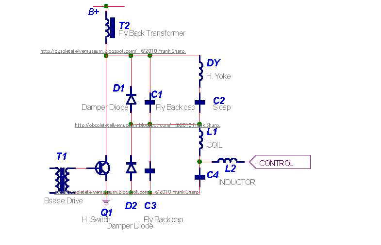 SPLIT DIODE MODULATOR
This horizontal circuit consists of two parts. D1, C1, C2 and DY are the components as described above.
D2, C3, C4 and L1 are a second “dummy” horizontal section that does not cause deflection current. By the
D.C. analyzing this circuit the voltage across C2 + C4 must equal the supply voltage (B+). Deflection
current in the DY is related to the supply voltage minus the voltage across C4. For a maximum horizontal
size the control point must be held at ground. This causes the dummy section to not operate and the DY
section will get full supply voltage. If the control point is at 1/3 supply then the DY section will be
operating at 2/3 supply.
 Note: The impedance of (D1,C1,C2 and DY) and (D2,C3,C4 and L1) makes a voltage divider. If the
control point is not connected then there is some natural voltage on C4. Most split diode monitors are built
to pull power from the dummy section through L2 to ground. A single power transistor shunts from the
control point to ground. It is true that power can be supplied from some other supply through L2 to rise the voltage on C4. For maximum range a bi-directional power amplifier can drive the control point.
The most exciting feature if the split diode modulator is that the flyback pulse, as seen by the flyback
transformer, is the same size at all horizontal size settings.
HORIZONTAL SWITCH/DAMPER DIODE
On the right hand side of the screen, the H. switch transistor conducts current through the deflection yoke.This current comes from the S correction capacitors, which have a charge equal to the effective supply
voltage. The damper diode allows current for the left hand side of the screen to flow back through the
deflection yoke to the S capacitors.
FLYBACK CAPACITOR
The flyback capacitor connects the hot side of the yoke to ground. This component determines the size and
length of the flyback pulse. ‘Tuning the flyback capacitor’ is done to match the timing of the flyback pulse
to the video blanking time of the video signal. The peak flyback voltage on the horizontal switch must be
set to less that 80% if the Vces specification. The two conditions of time and voltage can be set by three
variables (supply voltage, retrace capacitor and yoke inductance) .
S CAPACITOR
The S capacitors corrects outside versus center linearity in the horizontal scan. The voltage on the S cap
has a parabola plus the DC horizontal supply. Reducing the value of S cap increases this parabola thus
reducing the size of the outside characters and increasing the size of the center characters.
S Capacitor value: Too low: picture will be squashed towards edges.
Too high: picture will be stretched towards edges.
By simply putting a capacitor in series with each coil, the sawtooth waveform ismodified into a slightly sine-wave shape. This reduces the scanning speed near the
edges where the yoke is more sensitive. Generally the deflection angle of the electron
beam and the yoke current are closely related. The problem is the deflection angle
verses the distance of movement on the CRT screen does not have a linear effect.
BASE DRIVE CURRENT
The base drive resistor determines the amount of
base drive. If the transistor is over driven the Vsat
looks very good, but the current fall time is poor.
If the base current is too small the current fall time is very fast. The problem is that the transistor will have many volts across C-E when closed.
The best condition is found by placing the transistor in the heaviest load condition. Adjust the base resistor for the least power consumption then increase the base drive a small amount. This will slightly over drive the base.
BU208(A)
Silicon NPNnpn transistors,pnp transistors,transistors
Category: NPN Transistor, Transistor
MHz: <1 MHz
Volts: 1500V
HIGH VOLTAGE CAPABILITY
JEDEC TO-3 METAL CASE.
DESCRIPTION
The BU208A, BU508A and BU508AFI are
manufactured using Multiepitaxial Mesa
technology for cost-effective high performance
and use a Hollow Emitter structure to enhance
switching speeds.
APPLICATIONS:
* HORIZONTAL DEFLECTION FOR COLOUR TV With 110° or even 90° degree of deflection angle.
ABSOLUTE MAXIMUM RATINGS
Symbol Parameter Value Unit
VCES Collector-Emit ter Voltage (VBE = 0) 1500 V
VCEO Collector-Emit ter Voltage (IB = 0) 700 V
VEBO Emitter-Base Voltage (IC = 0) 10 V
IC Collector Current 8 A
ICM Collector Peak Current (tp < 5 ms) 15 A
TO - 3 TO - 218 ISOWATT218
Ptot Total Dissipation at Tc = 25 oC 150 125 50 W
Tstg Storage Temperature -65 to 175 -65 to 150 -65 to 150 oC
Tj Max. Operating Junction Temperature 175 150 150 °C


REX (ZANUSSI) 22RT411 "MADEIRA" CHASSIS BS400 DESCRIPTIONS OF THE UNITS AND THEIR FUNCTIONS:
- BS394.2 POWER SUPPLY WITH BU326A It
converts the mains voltage in DC voltage available at five outputs
with values of: +2OOV; +15OV; +27V (two outputs); +12.6V. These
voltages are stabilized and separated from the mains.REX (ZANUSSI) 22RT411 "MADEIRA" CHASSIS BS400 Switching power supply, especially for a T.V. receiving apparatus:
REX (ZANUSSI) 22RT411 "MADEIRA" CHASSIS BS400 Schaltnetzteil
(ZANUSSI BS394 SWITCH MODE POWER SUPPLY), IN GERMAN:
1. Schaltnetzteil,
insbesondere f·ur einen Fernsehempf·anger, mit einer Arbeitswicklung
(5), einem Schalttransistor (6), einer R·uckkopplungswicklung (7) und
einer Regelschaltung (ii) auf der Prim·arseite sowie mit Gleichrichtern
(15,16, 20) zur Erzeugung von Betriebsspannungen (U11U2#U3) auf der
Sekund·arseite eines Trenntransformators (1) gekenn zeichnet durch
folgende Merkmale: a) An eine Wicklung (19) ist ein Thyristor (24)
angeschlos sen, der f·ur die w·ahrend der siromf·uhrenden Phase der
Schalttransistoren (6) an der Wicklung (19) auftreten de Spannung in
Durchlassrichtung gepolt ist. b) An die Steuerelektrode des Thyristors
(24) ist eine der Betriebsspannungen (U2) in solcher H·ohe angelegt,
dass der Thyristor (24) im Normalbetrieb gesperrt bleibt und bei einem
unzul·assigen Anstieg der Betriebs spannung (U3) z·undet.

2. Netzteil nach Anspruch 1, dadurch gekennzeichnet, dass die Betriebsspannung (U3) ·uber einen Spannungsteiler (25,26) an die Steuerelektrode des Thyristors (24) angelegt ist.
3. Netzteil nach Anspruch 1, dadurch gekennzeichnet, dass die Wicklung (19) eine Sekund·arwicklung des Trenntransforma tors (1) ist.
Description:
Schaltnetzteil, insbesondere f·ur einen Fernsehempf·anger
 Bei
Ger·aten der Nachrichtentechnik wie z.B. einem Fernsehempf·anger ist es
bekannt, die f·ur die einzelnen Stufen notwendigen Betriebsspannungen
mit einem Schaltnetzteil aus der Netzspannung zu erzeugen (Funkschau
1975, Heft 5, Seite 40-43). Ein Schaltnetzteil erm·oglicht die f·ur den
Anschluss ·ausserer Ger·ate und f·ur die Massnahmen zur Schutzisolierung
vorteilhafte galvanische Trennung der Empf·angerschaltung vom Netz. Da
ein Schaltnetzteil mit einer gegen·uber der Netzfrequenz hohen Frequenz
von ca. 30 kHz arbeitet, kann der zur galvanischen Trennung dienende
Trenntransformator gegen·uber einem Netztrafo f·ur 50 Hz wesentlich
kleiner und leichter ausgebildet sein. Durch mehrere Wicklungen oder
Wicklungsabgriffe und angeschlossene Gleichrichter k·onnen auf der
Sekund·arseite des Trenntransformators Betriebs~ spannungen
unterschiedlicher Gr·osse und Polarit·at erzeugt werden.
Bei
Ger·aten der Nachrichtentechnik wie z.B. einem Fernsehempf·anger ist es
bekannt, die f·ur die einzelnen Stufen notwendigen Betriebsspannungen
mit einem Schaltnetzteil aus der Netzspannung zu erzeugen (Funkschau
1975, Heft 5, Seite 40-43). Ein Schaltnetzteil erm·oglicht die f·ur den
Anschluss ·ausserer Ger·ate und f·ur die Massnahmen zur Schutzisolierung
vorteilhafte galvanische Trennung der Empf·angerschaltung vom Netz. Da
ein Schaltnetzteil mit einer gegen·uber der Netzfrequenz hohen Frequenz
von ca. 30 kHz arbeitet, kann der zur galvanischen Trennung dienende
Trenntransformator gegen·uber einem Netztrafo f·ur 50 Hz wesentlich
kleiner und leichter ausgebildet sein. Durch mehrere Wicklungen oder
Wicklungsabgriffe und angeschlossene Gleichrichter k·onnen auf der
Sekund·arseite des Trenntransformators Betriebs~ spannungen
unterschiedlicher Gr·osse und Polarit·at erzeugt werden.
Ein solches Schaltnetzteil enth·alt eine Regelschaltung zur Stabilisierung der Amplitude der auf der Sekund·arseite erzeugten Betriebsspannungen. In dieser Regelschaltung wird eine durch Gleichrichtung der Impulsspannung am Trafo gewonnene Stellgr·osse erzeugt und mit einer Bezugsspannung verglichen. In Abh·angigkeit von der Abweichung wird der Schaltzeitpunkt des auf der Prim·arseite vorgesehenen elektronischen Schalters so gesteuert, dass die Amplitude der erzeugten Betriebsspannungen konstant bleibt.
Bei einem solchen Schaltnetzteil kann die genannte Regelschaltung z.B. durch ein fehlerhaftes Bauteil ausfallen. Die Regelung der Amplitude der erzeugten Betriebsspannungen ist dann unkontrolliert. Die Betriebsspannungen k·onnen dann auf den doppelten oder dreifachen Wert ansteigen. Dadurch besteht die Gefahr, dass das Schaltnetzteil oder die an die Betriebsspannungen angeschlossenen Verbraucher wie z.B. der Heizfaden der Bildr·ohre oder der Zeilenendstufentransistor zerst·ort werden. Der Anstieg der Betriebsspannungen kann dar·uberhinaus einen Anstieg der im Fernsehempf·anger erzeugten Hochspannung und dadurch eine R·ontgenstrahlung ausl·osen.
Es ist auch ein Schaltnetzteil bekannt (DE-OS 27 27 332), bei dem zum Schutz gegen einen zu starken Anstieg der erzeugten Betriebsspannungen aus der Impulsspannung an der Prim·arseite des Trafos eine Stellgr·osse gewonnen wird, die beim ·Uberschreiten eines Schwellwertes den R·uckkopplungsweg unwirksam steuert. Durch die Unterbrechung des R·uckkopplungsweges kann das Schaltnetzteil nicht mehr schwingen, so dass in erw·unschter Weise auch keine Betriebsspannungen mehr erzeugt werden. Diese Schaltung erfordert jedoch eine Vielzahl von Bauteilen und ist daher relativ teuer.
Der Erfindung liegt die Aufgabe zugrunde, eine sicher wirkende Schutzschaltung mit verringertem Schaltungsaufwand gegen die oben
beschriebenen Gefahren zu schaffen.
die oben
beschriebenen Gefahren zu schaffen.
Diese Aufgabe wird durch die im Anspruch 1 beschriebene Erfindung gel·ost. Vorteilhafte Weiterbildungen der Erfindung sind in den Unteranspr·uchen beschrieben.
Die Erfindung beruht auf folgender ·Uberlegung: Der Schalttransistor auf der Prim·arseite wird von der prim·arseitigen R·uckkopplungswicklung w·ahrend seiner stromleitenden Phase mit einem Basisstrom angesteuert. Wenn jetzt eine Sekund·arwicklung w·ahrend dieser stromleitenden Phase stark belastet, z.B. ·uber den Thyristor kurzgeschlossen wird, bricht auch die Spannung an der prim·arseitigen R·uckkopplungswicklung zusammen. Diese Wicklung kann dann f·ur den Schalttransistor nicht mehr einen f·ur den leitenden Betrieb ausreichenden Basis strom liefern. Das Schaltnetzteil schwingt dann nicht mehr, so dass die sekund·arseitigen Betriebsspannungen in erw·unschter Weise zusammenbrechen. Der schaltungstechni- sche Aufwand ist gering. Er besteht vorzugsweise aus einem Thyristor und zwei Widerst·anden.
Ein Ausf·uhrungsbeispiel der Erfindung wird anhand der Zeichnung erl·autert. Darin zeigen Figur 1 ein erfindungsgem·ass ausgebildetes Schaltnetzteil und Figur 2 Kurven zur Erl·auterung der Wirkungsweise. Dabei zeigen die kleinen Buchstaben, an welchen Punkten in Figur 1 die Spannungen gem·ass Figur 2 stehen.
Das
Schaltnetzteil gem·ass Figur 1 enth·alt auf der Prim·arseite des
Trenntransformators 1 den Netzgleichrichter 2, den Ladekondensator 3,
den Strom-Messwiderstand 4, die Prim·arwicklung 5 den Schalttransistor
6, die zur Schwingungserzeugung dienende R·uckkopplungswicklung 7, den
zur Steuerung des Schalttransistors 6 dienenden Thyristor 8, die
Regelwicklung 9, den zur Erzeugung der Regelspannung dienenden
Gleichrichter 10 sowie die zur Stabilisierung der Betriebsspannungen
dienende Regelschaltung 11 mit dem Transistor 12 und der eine
Referenzspannung lieferndenZenerdiode 13. Die Sekund·arwicklung 14
liefert ·uber den Gleichrichter 15 eine erste Betriebsspannung U1 von
150 V. Ein Abgriff der Wicklung 14 liefert ·uber den Gleichrichter 16
eine zweite Betriebsspannung U2 von 12 V f·ur einen
Fernbedienungsempf·anger.
Eine weitere Sekund·arwicklung 19 liefert ·uber den Gleichrichter 20 eine dritte Betriebsspannung U3 von 12 V. Die Polung der Wicklungen 14,19 und der Gleichrichter 15,16,20 ist derart, dass die Gleichrichter 15,16,20 w·ahrend der Sperrphase des Schalttransistors 6 durch die sekund·arseitig auftretenden Impulsspannungen leitend gesteuert sind und die angeschlossenen Ladekondensatoren aufladen.
An das untere Ende der Wicklung 19 ist zus·atzlich der Thyristor 24 angeschlossen. An die Steuerelektrode b des Thyristors 24 ist die Betriebs spannung U2 ·uber den Spannungsteiler 25,26 angelegt.
Die Wirkungsweise der Schaltung wird anhand der Figur 2 erl·autert. Es sei angenommen, dass das Schaltnetzteil im Zeitpunkt tl in Betrieb genommen wird. Mit der Diode 21 wird aus der Netzspannung am Punkt d ein positiver Impuls erzeugt. Dieser gelangt ·uber den Kondensator 23 auf die Basis des Schalttransistors 6 und steuert diesen leitend. Dadurch beginnt das Schaltnetzteil zu schwingen, wobei die Schwingung durch die R·uckkopplungswicklung 7
aufrechterhalten wird. Am Punkt a entsteht dann eine m·aanderf·ormige
Wechselspannung mit einer Frequenz von etwa 25-30 kHz.
Die daraufhin in den Sekund·arwicklungen 14,19 erzeugten Impulse erzeugen in der beschriebenen Weise die Betriebsspannungen U1,U2,U3. Der Spannungsteiler 25,26 ist so bemessen, dass der Thyristor 24 gesperrt bleibt, d.h. die Spannung am Punkt 6 jst kleiner als 0,7 V. Der Thyristor 24 hat dann keine Wirkung. Dir Amplitude der Spannungen Ui,U2,U3 wird ·uber die Regelschaltung 11 stabilisiert.
Es sei jetzt angenommen, dass durch einen Fehler in der Regelschaltung 11, z.B. durch Ausfall eines Bauteiles, die Regelung zur Stabilisierung der Betriebsspannungen U1,U2,U3 nicht mehr wirkt und diese Betriebsspannungen stark ansteigen. Dadurch steigt auch die Spannung am Punkt b an.
Im Zeitpunkt t2 erreicht diese Spannung den Wert von 0,7 V, so dass der Thyristor 24 z·undet. Der untere Teil der Wicklung 19 ist jetzt praktisch kurzgeschlossen. Das Netzteil ist dadurch sekund·arseitig so stark belastet, dass die R·uck kopplungswicklung 7 keinen ausreichenden Basisstrom zur Steuerung des Schalttransistors 6 in seine stromleitende Phase mehr liefert. Im Zeitpunkt t2 bricht die Schwingung des Schaltnetzteiles ab, so dass auch die Wechselspannung am Punkt a auf null abf·allt. Den Ladekondensatoren der Gleichrichter 15,16,20 wird kein Strom mehr zugef·uhrt, so dass die Betriebspannungen U1,U2,U3 nicht weiter ansteigen k·onnen, sondern entsprechend den wirksamen Entladezeitkonstanten abfallen. Das Schaltnetzteil w·urde auf diese Weise an sich beliebig lange ausgeschaltet bleiben.
Im Zeitpunkt t3 erscheint am Punkt b der n·achste aus der Netzspannung gewonnene Startimpuls, der den Schalttransistor 6 wieder leitend steuert, so dass die Wechselspannung am Punkt a wieder auftritt. Das Schaltnetzteil geht also in einen getakteten Betrieb ·uber, bei dem die ·ubertragene Leistung entsprechend dem Zeitverh·altnis zwischen Einschaltphase und Ausschaltphase der Spannung am Punkt a betr·achtlich verringert ist. Die Betriebsspannungen U11U2,U3 k·onnen nicht mehr unzul·assig hohe Werte annehmen.
Ein solches Schaltnetzteil enth·alt eine Regelschaltung zur Stabilisierung der Amplitude der auf der Sekund·arseite erzeugten Betriebsspannungen. In dieser Regelschaltung wird eine durch Gleichrichtung der Impulsspannung am Trafo gewonnene Stellgr·osse erzeugt und mit einer Bezugsspannung verglichen. In Abh·angigkeit von der Abweichung wird der Schaltzeitpunkt des auf der Prim·arseite vorgesehenen elektronischen Schalters so gesteuert, dass die Amplitude der erzeugten Betriebsspannungen konstant bleibt.
Bei einem solchen Schaltnetzteil kann die genannte Regelschaltung z.B. durch ein fehlerhaftes Bauteil ausfallen. Die Regelung der Amplitude der erzeugten Betriebsspannungen ist dann unkontrolliert. Die Betriebsspannungen k·onnen dann auf den doppelten oder dreifachen Wert ansteigen. Dadurch besteht die Gefahr, dass das Schaltnetzteil oder die an die Betriebsspannungen angeschlossenen Verbraucher wie z.B. der Heizfaden der Bildr·ohre oder der Zeilenendstufentransistor zerst·ort werden. Der Anstieg der Betriebsspannungen kann dar·uberhinaus einen Anstieg der im Fernsehempf·anger erzeugten Hochspannung und dadurch eine R·ontgenstrahlung ausl·osen.
Es ist auch ein Schaltnetzteil bekannt (DE-OS 27 27 332), bei dem zum Schutz gegen einen zu starken Anstieg der erzeugten Betriebsspannungen aus der Impulsspannung an der Prim·arseite des Trafos eine Stellgr·osse gewonnen wird, die beim ·Uberschreiten eines Schwellwertes den R·uckkopplungsweg unwirksam steuert. Durch die Unterbrechung des R·uckkopplungsweges kann das Schaltnetzteil nicht mehr schwingen, so dass in erw·unschter Weise auch keine Betriebsspannungen mehr erzeugt werden. Diese Schaltung erfordert jedoch eine Vielzahl von Bauteilen und ist daher relativ teuer.
Der Erfindung liegt die Aufgabe zugrunde, eine sicher wirkende Schutzschaltung mit verringertem Schaltungsaufwand gegen
die oben
beschriebenen Gefahren zu schaffen.Diese Aufgabe wird durch die im Anspruch 1 beschriebene Erfindung gel·ost. Vorteilhafte Weiterbildungen der Erfindung sind in den Unteranspr·uchen beschrieben.
Die Erfindung beruht auf folgender ·Uberlegung: Der Schalttransistor auf der Prim·arseite wird von der prim·arseitigen R·uckkopplungswicklung w·ahrend seiner stromleitenden Phase mit einem Basisstrom angesteuert. Wenn jetzt eine Sekund·arwicklung w·ahrend dieser stromleitenden Phase stark belastet, z.B. ·uber den Thyristor kurzgeschlossen wird, bricht auch die Spannung an der prim·arseitigen R·uckkopplungswicklung zusammen. Diese Wicklung kann dann f·ur den Schalttransistor nicht mehr einen f·ur den leitenden Betrieb ausreichenden Basis strom liefern. Das Schaltnetzteil schwingt dann nicht mehr, so dass die sekund·arseitigen Betriebsspannungen in erw·unschter Weise zusammenbrechen. Der schaltungstechni- sche Aufwand ist gering. Er besteht vorzugsweise aus einem Thyristor und zwei Widerst·anden.
Ein Ausf·uhrungsbeispiel der Erfindung wird anhand der Zeichnung erl·autert. Darin zeigen Figur 1 ein erfindungsgem·ass ausgebildetes Schaltnetzteil und Figur 2 Kurven zur Erl·auterung der Wirkungsweise. Dabei zeigen die kleinen Buchstaben, an welchen Punkten in Figur 1 die Spannungen gem·ass Figur 2 stehen.
Eine weitere Sekund·arwicklung 19 liefert ·uber den Gleichrichter 20 eine dritte Betriebsspannung U3 von 12 V. Die Polung der Wicklungen 14,19 und der Gleichrichter 15,16,20 ist derart, dass die Gleichrichter 15,16,20 w·ahrend der Sperrphase des Schalttransistors 6 durch die sekund·arseitig auftretenden Impulsspannungen leitend gesteuert sind und die angeschlossenen Ladekondensatoren aufladen.
An das untere Ende der Wicklung 19 ist zus·atzlich der Thyristor 24 angeschlossen. An die Steuerelektrode b des Thyristors 24 ist die Betriebs spannung U2 ·uber den Spannungsteiler 25,26 angelegt.
Die Wirkungsweise der Schaltung wird anhand der Figur 2 erl·autert. Es sei angenommen, dass das Schaltnetzteil im Zeitpunkt tl in Betrieb genommen wird. Mit der Diode 21 wird aus der Netzspannung am Punkt d ein positiver Impuls erzeugt. Dieser gelangt ·uber den Kondensator 23 auf die Basis des Schalttransistors 6 und steuert diesen leitend. Dadurch beginnt das Schaltnetzteil zu schwingen, wobei die Schwingung durch die R·uckk
opplungswicklung 7
aufrechterhalten wird. Am Punkt a entsteht dann eine m·aanderf·ormige
Wechselspannung mit einer Frequenz von etwa 25-30 kHz.Die daraufhin in den Sekund·arwicklungen 14,19 erzeugten Impulse erzeugen in der beschriebenen Weise die Betriebsspannungen U1,U2,U3. Der Spannungsteiler 25,26 ist so bemessen, dass der Thyristor 24 gesperrt bleibt, d.h. die Spannung am Punkt 6 jst kleiner als 0,7 V. Der Thyristor 24 hat dann keine Wirkung. Dir Amplitude der Spannungen Ui,U2,U3 wird ·uber die Regelschaltung 11 stabilisiert.
Es sei jetzt angenommen, dass durch einen Fehler in der Regelschaltung 11, z.B. durch Ausfall eines Bauteiles, die Regelung zur Stabilisierung der Betriebsspannungen U1,U2,U3 nicht mehr wirkt und diese Betriebsspannungen stark ansteigen. Dadurch steigt auch die Spannung am Punkt b an.
Im Zeitpunkt t2 erreicht diese Spannung den Wert von 0,7 V, so dass der Thyristor 24 z·undet. Der untere Teil der Wicklung 19 ist jetzt praktisch kurzgeschlossen. Das Netzteil ist dadurch sekund·arseitig so stark belastet, dass die R·uck kopplungswicklung 7 keinen ausreichenden Basisstrom zur Steuerung des Schalttransistors 6 in seine stromleitende Phase mehr liefert. Im Zeitpunkt t2 bricht die Schwingung des Schaltnetzteiles ab, so dass auch die Wechselspannung am Punkt a auf null abf·allt. Den Ladekondensatoren der Gleichrichter 15,16,20 wird kein Strom mehr zugef·uhrt, so dass die Betriebspannungen U1,U2,U3 nicht weiter ansteigen k·onnen, sondern entsprechend den wirksamen Entladezeitkonstanten abfallen. Das Schaltnetzteil w·urde auf diese Weise an sich beliebig lange ausgeschaltet bleiben.
Im Zeitpunkt t3 erscheint am Punkt b der n·achste aus der Netzspannung gewonnene Startimpuls, der den Schalttransistor 6 wieder leitend steuert, so dass die Wechselspannung am Punkt a wieder auftritt. Das Schaltnetzteil geht also in einen getakteten Betrieb ·uber, bei dem die ·ubertragene Leistung entsprechend dem Zeitverh·altnis zwischen Einschaltphase und Ausschaltphase der Spannung am Punkt a betr·achtlich verringert ist. Die Betriebsspannungen U11U2,U3 k·onnen nicht mehr unzul·assig hohe Werte annehmen.
- BS395.1 LINE DEFLECTION OUTPUT UNIT WITH BU208A (MOTOROLA) This p.c.b. amplifies the pulse sequence at line frequency and drives a circuit operating asan ON-OFF switch for supplying the deflection current to the horizontal yoke. It also
receives the parabolic signal which acts on the diodes modulator for E/W correction.
- BS396.3 SYNCHRONIZATION + E/W CORRECTION The p.c.b. processes the videosignal. Said process consists in separating the horizontal signals from the video composite
signal. The "pincushion correction" section receives a Sawtooth shaped signal and converts it into a parabolic shape for E/W correction.
- BS397.1 FRAME DEFLECTION WITH TDA1170 This p.c.b. generates a sawtoothvoltage at frame frequency which is used for driving the vertical deflection yoke. It supplies a
similar voltage to the "pincushion" section of the synchro. separator p.c.b. to obtain the E/W pincushion correction. It supplies a frame frequency pulse which is used for the luminance, chrominance and video amplifier p.c.b. blankings. It receives the vertical synchro.
from the synchro. separator p.c.b. and receives from the chassis a voltage proportional to the beam current.TDA1170 vertical deflection FRAME DEFLECTION INTEGRATED CIRCUITGENERAL DESCRIPTION f The TDA1170 and TDA1270 are monolithic integrated
circuits designed for use in TV vertical deflection systems. They are manufactured using
the Fairchild Planar* process.
Both devices are supplied in the 12-pin plastic power package with the heat sink fins bent
for insertion into the printed circuit board.
The TDA1170 is designed primarily for large and small screen black and white TV
receivers and industrial TV monitors. The TDA1270 is designed primarily for driving
complementary vertical deflection output stages in color TV receivers and industrial
monitors.
APPLICATION INFORMATION (TDA1170)
The vertical oscillator is directly synchronized by the sync pulses (positive or negative); therefore its free
running frequency must be lower than the sync frequency. The use of current feedback causes the yoke
current to be independent of yoke resistance variations due to thermal effects, Therefore no thermistor is
required in series with the yoke. The flyback generator applies a voltage, about twice the supply voltage, to
the yoke. This produces a short flyback time together with a high useful power to dissipated power
ratio.
- BS399.0 LUMINANCE AND CHROMINANCE + RGB AMPLIFIER This p.c.b. processes thecomplete composite video signal coming from the IF p.c.b. andsupplies the R-G-B signals to
the picture tube.
- BS398 TUNER + AFC + IF Conversion of the RF signal into an IF signal(video carrier:39.5 M z; audio carrier:33.5 MHZ).
Detection of the IF signal into low frequency video and audio signals.
- BS389 REMOTE CONTROL DECODER WITH ITT SAA1251 This p.c.b. enables remotecontrol of the following functions: selection of 16 programmes; "+" or "-" adjustment; brightness
saturation adjustment; silencing; TV receiver switching.
- BS388.2 TUNING MEMORY AND SEARCH
Remote control p.c.b. The display indicates the programme selected.
Furthermore,this p.c.b. includes all pushbuttons for clockadjustment.No adjustments needed. Automatic searching of a TV station through a start command. Manual searching of a TV station through two commands (increment and decrement).
Inclusion-exclusion of the AFC circuit with LED display. Band indication displayed on
three LEDs. Tuning level indication with five LEDs. Memorization of 16 selected
programmes manually or remote control.
- BS392.2 ST-BY SUPPLY AND OPTOCOUPLER START STOP FEATURE. The p.c.b. includes circuits relevant to: mains filter, degaussing, remote control supply, start remote control.Nc adjustments needed. It includes circuits for clock supply and for switch-ON
programming.
- BS401 This p.c.b. receives the audio signal (not adjusted in volume) coming from p.c.b. BS 398, it adjusts it in amplitude and tone, it amplifies it and sends it to drive the two receiver’s loudspeakers (tweeter and woofer).
BU208A (MOTOROLA). Silicon NPN
npn transistors,pnp transistors,transistorsCategory: NPN Transistor, Transistor
MHz: <1 MHz
Amps: 5A
Volts: 1500V
HIGH VOLTAGE CAPABILITY
JEDEC TO-3 METAL CASE.
DESCRIPTION
The BU208A, BU508A and BU508AFI are
manufactured using Multiepitaxial Mesa
technology for cost-effective high performance
and use a Hollow Emitter structure to enhance
switching speeds.
APPLICATIONS:
* HORIZONTAL DEFLECTION FOR COLOUR TV With 110° or even 90° degree of deflection angle.
ABSOLUTE MAXIMUM RATINGS
Symbol Parameter Value Unit
VCES Collector-Emit ter Voltage (VBE = 0) 1500 V
VCEO Collector-Emit ter Voltage (IB = 0) 700 V
VEBO Emitter-Base Voltage (IC = 0) 10 V
IC Collector Current 8 A
ICM Collector Peak Current (tp < 5 ms) 15 A
TO - 3 TO - 218 ISOWATT218
Ptot Total Dissipation at Tc = 25 oC 150 125 50 W
Tstg Storage Temperature -65 to 175 -65 to 150 -65 to 150 oC
Tj Max. Operating Junction Temperature 175 150 150 °C
REX (ZANUSSI) 22RT411 "MADEIRA" CHASSIS BS400 Television receiver with an automatic station finding arrangement:
MOTOROLA TUNING MEMORY / MEMOTRONIC SYSTEM TECHNOLOGY.In a radio or television receiver containing an automatic station finder with a digital counter, a clock generator, and a digital-to-analog converter forming the tuning voltage for the varactors, a recall memory consisting of two series-connected parallel memories is connected in parallel with the digital counter. At a stop signal from the
1. A receiver having automatic station finding capability, comprising:
means for tuning said receiver in response to an applied voltage;
a controllable pulse generator;
means for starting said pulse generator;
circulating counter means having parallel inputs and outputs, a stepping input and a set input, said stepping input connected to and responsive to pulses from said pulse generator for providing a variable digital output;
digital-to-analog convert
means for sensing a received signal and for providing a stop signal to the pulse generator in response thereto, whereby said generator stops providing pulses and the analog voltage remains constant keeping the receiver tuned to the received signal;
memory means having parallel inputs connected to the parallel outputs of said counter means and parallel outputs connected to the parallel inputs of said counter means;
means associated with said memory means for causing the memory means to store a particular digital output from said counter means; and
means associated with the set input of said counter means for selectively causing the digital signal at the counter input to be transferred to the counter output.
2. A receiver as described in claim 1, wherein the memory means comprises: two series connected parallel memories each having a transfer input, a first of said parallel memories having parallel inputs connected to the parallel outputs of the counter means and having the transfer input connected to the stop signal means, a second of said parallel memories having parallel outputs connected to the parallel inputs of the counter means and having the transfer input connected to the means for starting said pulse generator.
3. A receiver as described in claim 2, wherein each of said parallel memories comprises a plurality of semiconductor voltage flip-flops.
4. A receiver as described in claim 2, wherein the two series connected parallel memories are incorporated in an integrated circuit module with the counter means.
5. A receiver as described in claim 2, wherein the transfer input of the first parallel memory is also connected to the means associated with the set input of the counter means.
6. A receiver as described in claim 1, additionally comprising:
an additional memory means having parallel inputs and outputs;
means for connecting the inputs of said additional memory means to the counter means output and the outputs of said additional memory means to the counter inputs;
means for causing said additional memory means to store a digital output; and
means for transferring the stored digital output to the counter means input through the connecting means.
7. A receiver as described in claim 6, additionally comprising gate means disposed at the outputs of the memory means and the additional memory means for selectively connecting either the additional memory means or the memory means to the input of the counter.
8. A receiver as described in claim 6, wherein the additional memory means comprises a plurality of memories and the connecting means comprises a plurality of station switches corresponding in number to the number of additional memories.
9. A receiver as described in claim 1, wherein each memory means comprises a number of flip-flops corresponding to the number of digits to be stored.
Description:
The p
 resent
invention relates to a radio or television receiver with an automatic
station finding arrangement which contains a pulse generator, a
circulating counter formed from semiconductor counting flip-flops and
having parallel inputs, a digital-to-analog converter converting the
count of the counter to a tuning voltage, and a start-stop circuit
acting on the flow of counting pulses and controlled over a start and at
least one stop line, and with a parallel memory connected between the
parallel outputs and parallel inputs of the counter.
resent
invention relates to a radio or television receiver with an automatic
station finding arrangement which contains a pulse generator, a
circulating counter formed from semiconductor counting flip-flops and
having parallel inputs, a digital-to-analog converter converting the
count of the counter to a tuning voltage, and a start-stop circuit
acting on the flow of counting pulses and controlled over a start and at
least one stop line, and with a parallel memory connected between the
parallel outputs and parallel inputs of the counter.
Such a radio receiver is known from, e.g., the journal "Funkschau 1971", pp. 535 to 538 and 587 to 589. With the aid of the free-running pulse generator, the up-counter, and the digital-to-analog converter, the automatic station finding arrangement generates a sawtoothlike tuning voltage for the varactors contained as frequency-setting tuning elements in the resonant circuits of the receiver's radio-frequency portion. If a transmitter is received which meets the receiving criteria set in the receiver, the pulse generator is stopped so that the tuning voltage now remains constant until the operator continues the automatic station finding operation by actuating a start switch.
It is frequently desirable to tune in once again the station at which the start switch for automatic station finding was actuated last - either for comparison or because of the more interesting program. To do this in the case of a receiver with provision for unidirectional automatic station search, the entire search range must be scanned once or several times by repeatedly actuating the start switch, depending on whether the desired station is detected immediately or not.
It is the object of the invention to provide measures for a receiver of the kind referred to by way of introduction which permit the transmitter received before the actuation of the start switch to be found again with a high degree of safety by simple manipulation.
The invention is characterized in that the parallel memory consists of two series-connected parallel memories having one transfer input each, that the transfer input of the (first) parallel memory, whose parallel inputs are connected to the parallel outputs of the counter, are connected directly or indirectly to the stop line, that the transfer input of the (second) parallel memory, whose parallel outputs are connected to the parallel inputs of the counter, is connected directly or indirectly to the start line, that the counter has a set input for through-connecting the parallel inputs of the counter to the flip-flops of the counter, and that a recall switch is connected to the set input of the counter.
Particularly advantageously, the memory locations of the two series-connected parallel memories are storage flip-flops using semiconductor technology. In that case it is possible to arrange the counter and the parallel memories on a common chip of an integrated-circuit module. Such a module has only two terminals more than a module formed by the counter only.
The measures characterized by the invention thus require, aside from an additional recall switch, no additional space and involve nearly no additional expense. To recall the station previously tuned in it is only necessary to depress a button, for example, whereby the receiver is safely tuned to the station's carrier wave even if at the instant of the depression the local received field strength is temporarily too low for sufficient reception.
The invention will now be described in more detail with reference to the accompanying drawing, showing, by way of example, two embodiments of the invention, and wherein:
FIG. 1 is a block diagram showing the radio- and intermediate-frequency portions of a receiver with an automatic station finding arrangement and a recall arrangement;
FIG. 2 shows diagrams a to g explaining the operation of the recall storage, and
FIG. 3 shows a receiver similar to the one of FIG. 1 in which the automatic station finding counter and the recall memories are arranged together on the chip of an integrated-circuit module.
The receivers shown in the block diagrams of FIGS. 1 and 3 have a radio-frequency-receiving section 1, an intermediate-frequency amplif ier
2, and a demodulator section 3, to whose output 4 are connected the
arrangements processing the modulation frequency. The tunable resonant
circuits of the radio-frequency section contain varactors as tuning
elements. Connected to the radio-frequency section is an automatic
station finding arrangement in which a digital-to-analog converter 5
generates from the count of a digital counter 7, which receives signals
at a stepping input T and advances at the rate of a pulse generator 6, a
nearly sawtooth-shaped tuning voltage for the varactors. With a
sufficient received field strength at the antenna 8 of the receiver a
signal is formed in the demodulator section 3 which signal can be used
as stop signal 9 to change the state of a start-stop circuit 10 which
may be a flip flop. In the "stop" state the start-stop circuit
interrupts the pulse generation or the pulse flow in the pulse generator
so that the receiver remains tuned to the station being received. By
operating a start-button switch 11 a start signal 12 is generated in the
receiver which signal places the start-stop circuit in the "automatic
station finding" state and thus continues the automatic station finding
operation until next station meeting the receiver's receiving
requirements is received.
ier
2, and a demodulator section 3, to whose output 4 are connected the
arrangements processing the modulation frequency. The tunable resonant
circuits of the radio-frequency section contain varactors as tuning
elements. Connected to the radio-frequency section is an automatic
station finding arrangement in which a digital-to-analog converter 5
generates from the count of a digital counter 7, which receives signals
at a stepping input T and advances at the rate of a pulse generator 6, a
nearly sawtooth-shaped tuning voltage for the varactors. With a
sufficient received field strength at the antenna 8 of the receiver a
signal is formed in the demodulator section 3 which signal can be used
as stop signal 9 to change the state of a start-stop circuit 10 which
may be a flip flop. In the "stop" state the start-stop circuit
interrupts the pulse generation or the pulse flow in the pulse generator
so that the receiver remains tuned to the station being received. By
operating a start-button switch 11 a start signal 12 is generated in the
receiver which signal places the start-stop circuit in the "automatic
station finding" state and thus continues the automatic station finding
operation until next station meeting the receiver's receiving
requirements is received.
In the embodiment of FIG. 1, two series-connected parallel memories 15 and 16 are connected, respectively, over two groups of lines 13 and 14 consisting of n lines each, between the n outputs Q 11 to Q n1 and the parallel inputs A 11 to A n1 of the digital counter 7 containing n counting flip-flops. Each parallel memory contains n storage flip-flops and, besides the parallel bit inputs and outputs B and X, a transfer input S. If a transfer signal appears at the transfer input, the parallel memory records the bit word applied its parallel inputs B 1 to B n , which erases the previously entered bit word and now, in turn, appears at the memory outputs X 1 to X n .
The transfer input S of the parallel memory 15, whose parallel inputs are connected over the group of lines 13 to the outputs of the counter 7, is connected to the stop line 17, while the transfer input S of the parallel memory 16, whose parallel outputs are connected over the group of lines 14 to the parallel inputs of the counter 7, is connected to the start line 18.
Connected to a set input P of the digital counters 7 is a switch 19 whose operation generates a set signal. The set signal sets the counter to a count which is equal to the bit word at the parallel inputs A 1 to A n of the counter. At the same time, the set signal acts over the line 20 and via an OR circuit provided for isolation on the transfer input S of the first parallel memory 15.
The diagrams a to g of FIG. 2 explain the operation of the automatic station finding arrangement in conjunction with the recall memories. In diagram a each of the blocks II, III, etc. represents the bit word for a count of the digital counter 7. The blocks in the diagrams b and c are the bit words which are stored in the parallel memories 15 and 16 and can be taken off the latter's parallel outputs, the blocks with equal Roman numerals (e.g. V) representing equal bit words. The diagram d shows the counting pulses 22 for the digital counter 7, the diagram e the stop pulses 9, the diagram f the start pulses 12, and the diagram g the set pulse 23 triggered by the recall switch 19.
The respective count from which the digital-to-analog converter 5 forms the tuning voltage for the varactors is applied simultaneously to the input of the digital-to-analog converter and, as a bit word (e.g. II, III, IV . . . , diagram a), to the input of the first parallel memory 15. At the occurence of a stop signal 9 during the automatic station finding operation, the stop signal 9 acts as a transfer signal on the first par
allel
memory 15, and the count (e.g. V, diagram a) at which the stop pulse
(e.g. 9a) was generated is entered into the first parallel memory 15 (V
in diagram b). At the next start pulse 12a triggered via the
start-button switch 11 the automatic station finding operation begins
anew, starting from the instantaneous count (e.g. V, diagram a) of the
counter. The start signal (12a in diagram f) acts as a transfer signal
on the transfer input S of the second parallel memory 16, whereby the
second parallel memory takes over the bit word (e.g. V) of the first.
The next stop signal (e.g. 9b, diagram e) at a new count (e.g. VIII,
diagram a) stops the automatic station search and enters the new count
as a bit word (e.g. VIII, diagram b) into the first parallel memory 15.
If the operator operates the recall switch 19 so as to recall the setting to the previously received station, the set pulse 23 triggered by the recall switch sets the counter 7 to the count (e.g. V, diagram a) of the bit word (e.g. V, diagram c) stored in the second parallel memory 16, and the newly set count is entered into the first parallel memory 15 (e.g. V, diagram b). The next start signal (e.g. 12b, diagram f) initiates the automatic station finding operation as described.
In the embodiment of FIG. 3, the two series-connected parallel memories 15 and 16 are incorporated on the chip of an integrated-circuit module 25 which also comprises the circulating digital counter 7 and, for exam ple, the circuit 26 of a station memory device. The station memory device has the memory inputs D 1 to D n and the memory outputs Y 1 to Y n
of its circuit 26 connected in parallel with the digital counter 7 in
the same manner as the recall memory consisting of the two
series-connected parallel memories 15 and 16. Therefore, gate circuits
27 and 28 are inserted between the parallel outputs of these memories
and the parallel inputs A 1 to A n of the
digital counter. The gate circuit 27 between the recall memory and the
counter is opened by the set signal of the recall switch 19. The gate
circuit 28 between the station memory and the counter is opened by the
set signal of a switch 29 for calling the bit word of a station
preselected by the station buttons 30. In front of the set input 8 of
the digital counter the two set signals are separated from one another
in an OR circuit 31.
ple, the circuit 26 of a station memory device. The station memory device has the memory inputs D 1 to D n and the memory outputs Y 1 to Y n
of its circuit 26 connected in parallel with the digital counter 7 in
the same manner as the recall memory consisting of the two
series-connected parallel memories 15 and 16. Therefore, gate circuits
27 and 28 are inserted between the parallel outputs of these memories
and the parallel inputs A 1 to A n of the
digital counter. The gate circuit 27 between the recall memory and the
counter is opened by the set signal of the recall switch 19. The gate
circuit 28 between the station memory and the counter is opened by the
set signal of a switch 29 for calling the bit word of a station
preselected by the station buttons 30. In front of the set input 8 of
the digital counter the two set signals are separated from one another
in an OR circuit 31.
In the embodiment of FIG. 3, the start-stop circuit 10 is designed in the manner of a flip-flop and can assume a "stop" state and an "automatic station finding" state. The transfer inputs S of the recall memory's parallel memories 15 and 16 are connected via the lines 32 and 33 to the outputs of the start-stop circuit. Since the signals at the outputs of the start-stop circuit are continuous signals, the lines 32 and 33 to the transfer inputs include pulse shapers 34 and 35, respectively.
In embodiments corresponding to FIG. 3 and having no station memory device, besides the circuit 26, the gate circuits 27 and 28 and the OR circuit 31 are omitted.
Such a radio receiver is known from, e.g., the journal "Funkschau 1971", pp. 535 to 538 and 587 to 589. With the aid of the free-running pulse generator, the up-counter, and the digital-to-analog converter, the automatic station finding arrangement generates a sawtoothlike tuning voltage for the varactors contained as frequency-setting tuning elements in the resonant circuits of the receiver's radio-frequency portion. If a transmitter is received which meets the receiving criteria set in the receiver, the pulse generator is stopped so that the tuning voltage now remains constant until the operator continues the automatic station finding operation by actuating a start switch.
It is frequently desirable to tune in once again the station at which the start switch for automatic station finding was actuated last - either for comparison or because of the more interesting program. To do this in the case of a receiver with provision for unidirectional automatic station search, the entire search range must be scanned once or several times by repeatedly actuating the start switch, depending on whether the desired station is detected immediately or not.
It is the object of the invention to provide measures for a receiver of the kind referred to by way of introduction which permit the transmitter received before the actuation of the start switch to be found again with a high degree of safety by simple manipulation.
The invention is characterized in that the parallel memory consists of two series-connected parallel memories having one transfer input each, that the transfer input of the (first) parallel memory, whose parallel inputs are connected to the parallel outputs of the counter, are connected directly or indirectly to the stop line, that the transfer input of the (second) parallel memory, whose parallel outputs are connected to the parallel inputs of the counter, is connected directly or indirectly to the start line, that the counter has a set input for through-connecting the parallel inputs of the counter to the flip-flops of the counter, and that a recall switch is connected to the set input of the counter.
Particularly advantageously, the memory locations of the two series-connected parallel memories are storage flip-flops using semiconductor technology. In that case it is possible to arrange the counter and the parallel memories on a common chip of an integrated-circuit module. Such a module has only two terminals more than a module formed by the counter only.
The measures characterized by the invention thus require, aside from an additional recall switch, no additional space and involve nearly no additional expense. To recall the station previously tuned in it is only necessary to depress a button, for example, whereby the receiver is safely tuned to the station's carrier wave even if at the instant of the depression the local received field strength is temporarily too low for sufficient reception.
The invention will now be described in more detail with reference to the accompanying drawing, showing, by way of example, two embodiments of the invention, and wherein:
FIG. 1 is a block diagram showing the radio- and intermediate-frequency portions of a receiver with an automatic station finding arrangement and a recall arrangement;
FIG. 2 shows diagrams a to g explaining the operation of the recall storage, and
FIG. 3 shows a receiver similar to the one of FIG. 1 in which the automatic station finding counter and the recall memories are arranged together on the chip of an integrated-circuit module.
The receivers shown in the block diagrams of FIGS. 1 and 3 have a radio-frequency-receiving section 1, an intermediate-frequency amplif
 ier
2, and a demodulator section 3, to whose output 4 are connected the
arrangements processing the modulation frequency. The tunable resonant
circuits of the radio-frequency section contain varactors as tuning
elements. Connected to the radio-frequency section is an automatic
station finding arrangement in which a digital-to-analog converter 5
generates from the count of a digital counter 7, which receives signals
at a stepping input T and advances at the rate of a pulse generator 6, a
nearly sawtooth-shaped tuning voltage for the varactors. With a
sufficient received field strength at the antenna 8 of the receiver a
signal is formed in the demodulator section 3 which signal can be used
as stop signal 9 to change the state of a start-stop circuit 10 which
may be a flip flop. In the "stop" state the start-stop circuit
interrupts the pulse generation or the pulse flow in the pulse generator
so that the receiver remains tuned to the station being received. By
operating a start-button switch 11 a start signal 12 is generated in the
receiver which signal places the start-stop circuit in the "automatic
station finding" state and thus continues the automatic station finding
operation until next station meeting the receiver's receiving
requirements is received.
ier
2, and a demodulator section 3, to whose output 4 are connected the
arrangements processing the modulation frequency. The tunable resonant
circuits of the radio-frequency section contain varactors as tuning
elements. Connected to the radio-frequency section is an automatic
station finding arrangement in which a digital-to-analog converter 5
generates from the count of a digital counter 7, which receives signals
at a stepping input T and advances at the rate of a pulse generator 6, a
nearly sawtooth-shaped tuning voltage for the varactors. With a
sufficient received field strength at the antenna 8 of the receiver a
signal is formed in the demodulator section 3 which signal can be used
as stop signal 9 to change the state of a start-stop circuit 10 which
may be a flip flop. In the "stop" state the start-stop circuit
interrupts the pulse generation or the pulse flow in the pulse generator
so that the receiver remains tuned to the station being received. By
operating a start-button switch 11 a start signal 12 is generated in the
receiver which signal places the start-stop circuit in the "automatic
station finding" state and thus continues the automatic station finding
operation until next station meeting the receiver's receiving
requirements is received. In the embodiment of FIG. 1, two series-connected parallel memories 15 and 16 are connected, respectively, over two groups of lines 13 and 14 consisting of n lines each, between the n outputs Q 11 to Q n1 and the parallel inputs A 11 to A n1 of the digital counter 7 containing n counting flip-flops. Each parallel memory contains n storage flip-flops and, besides the parallel bit inputs and outputs B and X, a transfer input S. If a transfer signal appears at the transfer input, the parallel memory records the bit word applied its parallel inputs B 1 to B n , which erases the previously entered bit word and now, in turn, appears at the memory outputs X 1 to X n .
The transfer input S of the parallel memory 15, whose parallel inputs are connected over the group of lines 13 to the outputs of the counter 7, is connected to the stop line 17, while the transfer input S of the parallel memory 16, whose parallel outputs are connected over the group of lines 14 to the parallel inputs of the counter 7, is connected to the start line 18.
Connected to a set input P of the digital counters 7 is a switch 19 whose operation generates a set signal. The set signal sets the counter to a count which is equal to the bit word at the parallel inputs A 1 to A n of the counter. At the same time, the set signal acts over the line 20 and via an OR circuit provided for isolation on the transfer input S of the first parallel memory 15.
The diagrams a to g of FIG. 2 explain the operation of the automatic station finding arrangement in conjunction with the recall memories. In diagram a each of the blocks II, III, etc. represents the bit word for a count of the digital counter 7. The blocks in the diagrams b and c are the bit words which are stored in the parallel memories 15 and 16 and can be taken off the latter's parallel outputs, the blocks with equal Roman numerals (e.g. V) representing equal bit words. The diagram d shows the counting pulses 22 for the digital counter 7, the diagram e the stop pulses 9, the diagram f the start pulses 12, and the diagram g the set pulse 23 triggered by the recall switch 19.
The respective count from which the digital-to-analog converter 5 forms the tuning voltage for the varactors is applied simultaneously to the input of the digital-to-analog converter and, as a bit word (e.g. II, III, IV . . . , diagram a), to the input of the first parallel memory 15. At the occurence of a stop signal 9 during the automatic station finding operation, the stop signal 9 acts as a transfer signal on the first par
If the operator operates the recall switch 19 so as to recall the setting to the previously received station, the set pulse 23 triggered by the recall switch sets the counter 7 to the count (e.g. V, diagram a) of the bit word (e.g. V, diagram c) stored in the second parallel memory 16, and the newly set count is entered into the first parallel memory 15 (e.g. V, diagram b). The next start signal (e.g. 12b, diagram f) initiates the automatic station finding operation as described.
In the embodiment of FIG. 3, the two series-connected parallel memories 15 and 16 are incorporated on the chip of an integrated-circuit module 25 which also comprises the circulating digital counter 7 and, for exam
 ple, the circuit 26 of a station memory device. The station memory device has the memory inputs D 1 to D n and the memory outputs Y 1 to Y n
of its circuit 26 connected in parallel with the digital counter 7 in
the same manner as the recall memory consisting of the two
series-connected parallel memories 15 and 16. Therefore, gate circuits
27 and 28 are inserted between the parallel outputs of these memories
and the parallel inputs A 1 to A n of the
digital counter. The gate circuit 27 between the recall memory and the
counter is opened by the set signal of the recall switch 19. The gate
circuit 28 between the station memory and the counter is opened by the
set signal of a switch 29 for calling the bit word of a station
preselected by the station buttons 30. In front of the set input 8 of
the digital counter the two set signals are separated from one another
in an OR circuit 31.
ple, the circuit 26 of a station memory device. The station memory device has the memory inputs D 1 to D n and the memory outputs Y 1 to Y n
of its circuit 26 connected in parallel with the digital counter 7 in
the same manner as the recall memory consisting of the two
series-connected parallel memories 15 and 16. Therefore, gate circuits
27 and 28 are inserted between the parallel outputs of these memories
and the parallel inputs A 1 to A n of the
digital counter. The gate circuit 27 between the recall memory and the
counter is opened by the set signal of the recall switch 19. The gate
circuit 28 between the station memory and the counter is opened by the
set signal of a switch 29 for calling the bit word of a station
preselected by the station buttons 30. In front of the set input 8 of
the digital counter the two set signals are separated from one another
in an OR circuit 31. In the embodiment of FIG. 3, the start-stop circuit 10 is designed in the manner of a flip-flop and can assume a "stop" state and an "automatic station finding" state. The transfer inputs S of the recall memory's parallel memories 15 and 16 are connected via the lines 32 and 33 to the outputs of the start-stop circuit. Since the signals at the outputs of the start-stop circuit are continuous signals, the lines 32 and 33 to the transfer inputs include pulse shapers 34 and 35, respectively.
In embodiments corresponding to FIG. 3 and having no station memory device, besides the circuit 26, the gate circuits 27 and 28 and the OR circuit 31 are omitted.
No comments:
Post a Comment
The most important thing to remember about the Comment Rules is this:
The determination of whether any comment is in compliance is at the sole discretion of this blog’s owner.
Comments on this blog may be blocked or deleted at any time.
Fair people are getting fair reply. Spam and useless crap and filthy comments / scrapers / observations goes all directly to My Private HELL without even appearing in public !!!
The fact that a comment is permitted in no way constitutes an endorsement of any view expressed, fact alleged, or link provided in that comment by the administrator of this site.
This means that there may be a delay between the submission and the eventual appearance of your comment.
Requiring blog comments to obey well-defined rules does not infringe on the free speech of commenters.
Resisting the tide of post-modernity may be difficult, but I will attempt it anyway.
Your choice.........Live or DIE.
That indeed is where your liberty lies.
Note: Only a member of this blog may post a comment.