


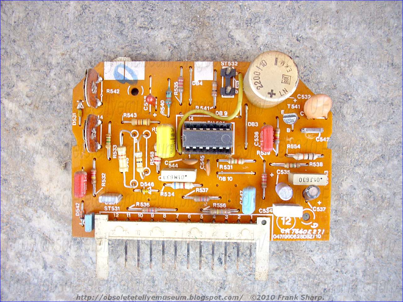


 CHASSIS 712A SUPPLY UNIT (NETZTEIL SM)
AT 349354065
This is a SMPS Supply unit which seems simple but is not !
- 3 SUB Units are composing the FINAL device unit
1 - MAINS RECTIFIER + DEGAUSS PTC + BOBBIN FILTERS + CAPS (burned !! !!!) BS422
ET 309378996 (NETZEINGANG)
2 - Pulse Command unit with S417T (Telefunken) BS423 AT349354067 (ANSTEUERUNG)
3 - Secondary Voltages Generation and separation (With a LM317) BS426 AT349354068
(SEC.SPANNUNGSERZEUGUNG).
CHASSIS 712A SUPPLY UNIT (NETZTEIL SM)
AT 349354065
This is a SMPS Supply unit which seems simple but is not !
- 3 SUB Units are composing the FINAL device unit
1 - MAINS RECTIFIER + DEGAUSS PTC + BOBBIN FILTERS + CAPS (burned !! !!!) BS422
ET 309378996 (NETZEINGANG)
2 - Pulse Command unit with S417T (Telefunken) BS423 AT349354067 (ANSTEUERUNG)
3 - Secondary Voltages Generation and separation (With a LM317) BS426 AT349354068
(SEC.SPANNUNGSERZEUGUNG).
 1. In an infrared remote control transmitter for controlling a television system, apparatus comprising:
 a reference circuit point for receiving a reference potential;
a supply circuit point for receiving a DC supply voltage;
a battery connected with a predetermined polarity connected between said supply and reference circuit points;
at least one light-emitting diode for emitting infrared radiation when rendered conductive, said light emitting diode having a cathode and an anode, one of said cathode and anode being connected to said reference circuit point, said light-emitting diode being poled with respect to said reference circuit point so as to be conductive in response to the application of a voltage to the other one of said cathode and anode having the opposite polarity to said battery with respect to said reference circuit point and non-conductive in response to the application of a voltage to said other one of said cathode and anode having the same polarity as said battery with respect to said reference circuit point;
a source cir

cuit point for receiving an input signal having pulses encoded to represent information for controlling a predetermined function of said television receiver;
a drive circuit point;
a capacitor directly connected between said drive circuit point and said other one of said cathode and anode;
a diode directly connected between said other one of said cathode and anode and said reference circuit point and poled in the opposite sense to said light-emitting diode with respect to said reference circuit point;
push-pull amplifier means for developing a drive voltage at said drive point including first and second bipolar  transistors of opposite conduction types, each of said transistors having a collector-emitter path and a base electrode for controlling the conduction of said collector-emitter path, said collector-emitter path of said first transistor being directly connected between said supply circuit point and said drive circuit point, said collector-emitter path of said second transistor being connected between said drive circuit point and said reference point; and
input means coupled between said source circuit point and said bases of said first and second transistors for rendering said collector-emitter path of said first transistor conductive and said collector-emitter path of said second transistor non-conductive in response to a first portion of said pulses of said input signal and for rendering said collector-emitter path of said second transistor conductive and said collector-emitter path of said first transistor non-conductive in response to a second portion of said pulses of said input signal.
2. The apparatus recited in claim 1 wherein:three light-emitting diodes poled in the same direction are connected in series between said capacitor means and said reference circuit point.
3. The apparatus recited in claim 1 wherein:a second capacitor is directly connected between said drive point and said other one of said cathode and anode in parallel with said first mentioned capacitor directly connected between said drive point and said other one of said cathode and anode.
4. The apparatus recited in claim 1 wherein:said input means includes a first capacitor connected between said source circuit point and said base of said first transistor; first means connected between said supply circuit point and said base of said first transistor for discharging said first capacitor; a second capacitor connected between said source circuit point and said base of said second transistor; and second means connected between said base of said second transistor and said reference circuit point for discharging said second capacitor.
5. The apparatus recited in claim 4 wherein:said first means includes a further diode poled to be conductive when said collector-emitter path of said first transistor is non-conductive and non-conductive when said collector-emitter path of said first transistor is conductive; and
said second means includes a still further diode poled to be conductive when said collector-emitter path of said second transistor is non-conductive and non-conductive when said collector-emitter path of said second transistor is conductive.
6. In an infrared remote control transmitter for controlling a television system, apparatus comprising:a reference circuit point for receiving a reference potential;
a supply circuit point for receiving a DC supply voltage;
a battery connected with a predetermined polarity connected between said supply and reference circuit points;
three light-emitting diodes which emit infrared radiation when rendered conductive directly connected in series between a voltage application circuit point and said reference circuit point, all of said light-emitting diodes being poled with respect to said reference circuit point so as to be conductive in response to the application of a voltage to said voltage application circuit point having the opposite polarity to said battery with respect to said reference circuit point and non-conductive in response to the application of a voltage to said voltage application circuit point having the same polarity as said battery with respect to said reference circuit point;
a source circuit point for receiving an input signal having pulses encoded to represent information for controlling a predetermined function of said television receiver;
a drive circuit point;
a first capacitor directly connected between said drive circuit point and said voltage application circuit point;
a second capacitor directly connected between said drive circuit point and said voltage application circuit point;
a diode directly connected between said voltage application circuit point and said reference circuit point and poled in the opposite sense to said light-emitting diode with respect to said reference circuit point;

push-pull amplifier means for developing a drive voltage at said drive point including first and second bipolar transistors of opposite conduction types, each of said transistors having a collector-emitter path and a base electrode for controlling the conduction of said collector-emitter path, said collector-emitter path of said first transistor being directly connected between said supply circuit point and said drive circuit point, said collector-emitter path of said second transistor being connected between said drive circuit point and said reference point; and
input means coupled between said source circuit point and said bases of said first and second transistors for rendering said collector-emitter path of said first transistor conductive and said collector-emitter path of said second transistor non-conductive in response to a first portion of said pulses of said input signal and for rendering said collector-emitter path of said second transistor conductive and said collector-emitter path of said first transistor non-conductive in response to a second portion of said pulses of said input signal.
BACKGROUND OF THE PRESENT INVENTION
Th e present invention relates to drive circuits for infrared remote control transmitters.
Infrared remote control systems for television receivers and the like are known. The chief advantage of infrared remote control systems in comparison to ultrasonic remote control systems is that they are less susceptible to erroneously-generated interference signals. Unfortunately, the human eye may be harmed under conditions of prolonged, continuous and direct exposure to infrared radiation.
In order to reduce the possibility of harm to the eyes of users, infrared remote control systems utilize special pulse codes which minimize the duration of infrared radiation during the transmission of remote controlled messages. However, since in conventional drive circuits for infrared remote control transmitters the infrared light source, e.g., a light-emitting diode or diodes, is typically included in a direct current path from a supply voltage, infrared radiation may be continuously emitted should there be a component failure in the remote control transmitter. Therefore, there is a requirement for drive circuits for use in infrared remote control transmitters in which component failures do not result in the continuous emission of infrared radiation. The present invention concerns such a "fail-safe" drive circuit.
SUM MARY OF THE PRESENT INVENTION
In a remote control transmitter, at least one infrared light-emitting diode is coupled to a point of reference potential and poled so as to be substantially nonconductive in response to voltages having the same polarity as a DC supply voltage for the transmitter and substantially conductive in response to voltages having the polarity opposite to the polarity of the DC supply voltage. Driver means responsive to an input signal is coupled between the source of the DC supply voltage and the light-emitting diode. The driver means normally generates an alternating drive voltage for the light-emitting diode having portions with polarities both the same as and opposite to the polarity of the DC supply voltage. The driver means is arranged so that the portions of the drive signal having the polarity opposite to that of the DC supply voltage are at least inhibited when a component failure occurs.
BRIEF DESCRIPTION OF THE DRAWING
The sole FIGURE of the drawing shows, partially in block diagram form and partially in schematic diagram form, an infrared remote control system constructed in accordance with the present invention as it may be employed in a television receiver arrangement.
DETAILED DESCRIPTION OF THE DRAWING
A television receiver 1 includes an antenna 3, a tuner 5, an IF signal processing unit 7, a picture signal processing unit 9, a sound signal processing unit 11, a picture tube 13 and a speaker 15 arranged in a conventional fashion to produce visual and audio responses. A power supply 17 is selectively energized to generate DC supply voltages for the portions of the receiver so far described from the AC line voltage in response to an ON/OFF control signal generated by a remote control receiver 19. Receiver 1 also includes a standby power supply 20 which continuously couples a DC supply voltage to remote control receiver 19 so that it is ready to accept messages from a remote control transmitter 21.
Remote control receiver 19 includes a photosensitive diode 23. The conduction of photo diode 23 is controlled in response to encoded optical signals having frequencies in the infrared range generated by remote control transmitter 21. A detector 25 senses the changes in the conduction of diode 23 and generates electrical signals corresponding to the encoded optical signals. The electrical signals are decoded by a decoder 27 to generate the ON/OFF control signal for tuning receiver 1 on and off, a CHANNEL SELECTION control signal for controlling the frequency to which a tuner 5 is tuned, and a VOLUME control signal for controlling the sound level of receiver 1.
Remote control transmitter 21 includes a keyboard 29 including push buttons (not shown) by which a user may control the various receiver functions enumerated above. When a push button is depressed a corresponding electrical signal is generated by keyboard 29. A pulse encoder 31 is responsive to these electrical signals to generate respective coded pulse signals. The coded pulse signals are processed by a driver 33 to cause infrared light-emitting diodes 35, 37 and 39 to generate corresponding optical signals in the infrared frequency range.
Various codes for infrared remote control systems and encoders and decoders for these codes are known. For example, encoder 31 and decoder 27 may comprise S2600 and S2601 integrated circuits manufactured by American Microsystems, Inc. of Santa Clara, Calif.
The exact nature of the codes is not directly germane to the present invention. However, it is desirable for the reasons of safety discussed earlier that the code formats are arranged so that the duration of infrared radiation during a transmission is minimized. Since the pulses of the pulse signals generated by pulse encoder 31 correspond to the intervals of infrared radiation, this may be accomplished by causing the electrical pulse signals generated by encoder 31 to have a relatively low duty cycle, e.g., less than 20 percent. In addition, for safety reasons, it is desirable that light-emitting diodes 35, 37 and 39 be physically separated on transmitter 21 from one another by a distance selected so that the power of the infrared radiation they generate is distributed rather than concentrated in a relatively small area.
While these safety precautions to some extent minimize the danger to users, they do not account for component failures which may cause the continuous, i.e., DC, emission of infrared radiation. Unfortunately, the human eye may be injured when directly exposed to continuous infrared radiation for prolonged periods. While such situations are extremely rare, since they would involve not only a component failure but the misuse of the transmitter, they may occur under extraordinary circumstances. For example, a curious child may point an infrared transmitter with a failed component directly into his eye.
Drive circuit 33 is arranged to prevent the continuous emission of infrared radiation under any foreseeable component failure mode. Driver 33 includes a push-pull amplifier 41 comprising a PNP transistor 43 and an NPN transistor 45 having their collector-emitter junctions coupled in series between a battery 47 and signal ground. Battery 47 is the source of DC supply voltage for transmitter 21. The output of pulse encoder 31 is coupled to the bases of transistors 43 and 45 through capacitors 49 and 51, respectively. Diodes 53 and 55 are coupled in shunt with the base-emitter junctions of transistors 43 and 45, respectively. The junction of the collectors of transistors 43 and 45 is coupled through parallel connected capacitors 57 and 58 to the cathode of light-emitting diode 35. Light-emitting diodes 35, 37 and 39 are connected in series with the same polarity between capacitors 57 and 58 and signal ground. The polarity of light-emitting diodes 35, 37 and 39 is selected so that they are rendered nonconductive in response to the application of voltages to the cathode of light-emitting diode 35 having the same polarity (i.e., positive) with respect to signal ground as the DC supply voltage provided by battery 47 and only rendered conductive in response to the application of voltages having the opposite polarity (i.e., negative) with respect to signal ground to the DC supply voltage. A diode 59 is connected in shunt with series connected light-emitting diodes 35, 37 and 39 and poled in the opposite direction.
In operation, pulse encoder 31 generates a pulse signal encoded as described above. The pulse signal includes positive-going pulses. In response to the leading edges of the positive-going pulses, transistor 45 is rendered conductive. In response to the trailing edges of the positive-going pulses, transistor 43 is rendered conductive. Diodes 53 and 55 serve as discharge paths for capacitors 49 and 51 during the intervals when transistors 43 and 45, respectively, are nonconductive. Diodes 53 and 55 also clamp the voltage at the bases of transistors 43 and 45 close to the battery voltage and the voltage at signal ground, respectively, in order to protect the base-emitter junctions of transistors 43 and 45 from reverse breakdown failure voltages. Desirably, capacitors 49 and 51 have relatively small values so that capacitors 49 and 51 are charged and discharged in response to each pulse. As a result, transistors 43 and 45 are alternately rendered conductive and nonconductive in response to each pulse of the pulse signal.
When transistor 43 is conductive (and transistor 45 is nonconductive) capacitors 57 and 58 are charged from battery 47. When transistor 45 is conductive (and transistor 43 is nonconductive) capacitors 57 and 58 are discharged to signal ground. As a result, an alternating drive voltage, i.e., one having polarity excursions above and below the potential at signal ground, are generated at the cathode of light-emitting diode 35. Light-emitting diodes are conductive in response to the negative portions of the drive voltage and are nonconductive in response to the positive portions of the drive voltage. Diodes 35, 37 and 39 only emit infrared radiation when they are conductive. Therefore, infrared radiation is only emitted by transmitter 21 when the drive voltage has a polarity (i.e., negative opposite to the polarity of the DC supply voltage.
Desirably, the capacitance of the combination of capacitors 57 and 58 is relatively large, e.g., 1 microfarad, so that sufficient drive current is provided to light-emitting diodes 35, 37 and 39 to cause them to emit infrared radiation. For the same reason, two capacitors rather than one are used, since the effective series resistance associated with the parallel combination is smaller than the series resistance of a single capacitor.
In the event that there is a component failure within drive circuit 33, drive voltage developed at the cathode of light-emitting diode 35 will be reduced and, in most cases, substantially inhibited. Under these conditions, since the amplitude of the negative portions of the drive signal will at least have a lower than normal amplitude, the infrared radiation will have a lower than normal energy.
Briefly, any failure of a component within driver 33 causing the component to open or short, substantially prevents the development of an alternating drive signal at the cathode of light-emitting diode 35. Since diodes 35, 37 and 39 are rendered conductive only in response to negative-going voltages, no infrared radiation is generated. Any component failure between the extremes of an open or short causes a reduction in the amplitude of the alternating drive signal. By way of example, consider the following failure modes. If either transistor 43 or 45 fails, e.g., by shorting from collector to emitter, capacitors 57 and 58 will be either permanently charged or discharged, thereby preventing the development of an alternating drive signal. If one of capacitors 57 and 58 shorts, only positive-going voltages are developed at the cathode of light-emitting diode 35. If the collector to emitter junction of transistor 43 and one of capacitors 57 and 58 short, a DC signal is coupled to the cathode of light-emitting diode 35, thereby rendering diode 59 conductive and preventing light-emitting diodes 35, 37 and 39 from being rendered conductive. If diode 59 opens, capacitors 57 and 58 will not be charged thereby preventing the development of an alternating voltage at the cathode of diode 35. If diode 59 fails so as to lose its unidirectional conductive characteristics, i.e., in essence becomes a passive element, an alternating drive signal will be developed but it will have a lower than normal amplitude. Furthermore, failures in pulse encoder 31 causing generation of a DC signal rather than a pulse signal will also cause the loss of an alternating drive signal.
Driver circuit 33 may be modified in some respects without causing the loss of its "fail-safe" nature. For example, any or all of diodes 53, 55 and 59 may be replaced with resistors. While this modification causes a reduction in efficiency of the normal operation of drive circuit 33, it does not alter its "fail-safe" nature. These and other modifications are intended to be within the scope of the present invention as set forth in the following claims.
TELEFUNKEN CHASSIS 712A Tuning circuit arrangement
1. A circuit for adjusting a tuning circuit, the tuning circuit including at least one resonant circuit composed of a variable inductance and a variable capacitance constituted by at least one voltage-variable tuning diode, one side of the resonant circuit being connected to a point at circuit ground potential and adjustment of the resonant circuit being effected by changing the resonant circuit inductance and the resonant circuit capacitance, with changing of the resonant circuit capacitance being effected exclusively by varying the tuning voltage of the tuning diode, the tuning circuit further including a source of a variable tuning potential which is variable over a range between maximum and minimum extreme values, each extreme value being different from the circuit ground potential, and said circuit for adjusting comprising at least one adjustment potentiometer connected between a point of said source providing the variable tuning potential and a point of said source permanently providing one of said extreme values, said potentiometer having an adjustable tap connected to provide the tuning voltage for said tuning diode. 2. An arrangement as defined in claim 1 wherein said tuning circuit includes a plurality of said resonant circuits and said circuit for adjusting comprises a plurality of said potentiometers connected together in parallel and each having a respective adjustable tap connected to provide the tuning voltage for at least one respective tuning diode. 3. An arrangement as defined in claim 1 wherein said source comprises a tuning potentiometer connected to have a respective one of the extreme values of the tuning potential at each of its ends and having an adjustable tap providing the variable tuning potential, and said adjustment potentiometer is connected between one end and said movable tap of said tuning potentiometer. 4. An arrangement as defined in claim 1 wherein said tuning circuit includes at least two of said resonant circuits and said adjustable tap of said adjustment potentiometer is connected to provide the tuning voltage for said at least two resonant circuits. 5. An arrangement as defined in claim 4 wherein said resonant circuits have respectively different relative frequency variations. BACKGROUND OF THE INVENTION
The invention relates to a tuning circuit arrangement comprising one or more tuning circuits in which tuning diodes are provided for tuning of the frequency range. In such an arrangement, the adjustment of the tuned circuit takes place, for example, by changing the tuned circuit inductance and the tuned circuit capacitance.
As is known, tuning circuits have the object of tuning the resonant circuits of selective amplifiers and/or oscillators to a given resonant frequency. In a known tuning circuit, the adjustment to synchronous operation in each circuit takes place via a tuning coil and a particular trimmer capacitor. In the known tuning circuit arrangement a multiply repeated adjustment of the inductance and the capacitance is required for adjustment to synchronous operation, because the setting of the trimmer capacitors again changes the resonant frequency of the frequency previously set inductively.
SUMMARY OF THE INVENTION
It is an object of the invention to provide a tuning circuit arrangement with simplified adjustment.
According to a first aspect of the invention, there is provided a tuning circuit arrangement comprising one or more tuned circuits, tuning diodes in said tuned circuits for tuning the frequency range of said tuned circuits and means for varying the tuning voltage of said tuning diodes for providing exclusive variation of the tuned circuit capacitance of said tuned circuit.
According to a second aspect of the invention, there is provided a tuning circuit arrangement comprising one or more tuning circuits, in which tuning diodes are provided for the purpose of tuning the frequency range and in which the tuned circuit adjustment takes place by changing the tuned circuit inductance and the tuned circuit capacitance, characterized in that the adjustment in capacitance takes place exclusively by varying the tuning voltage for the tuning diode(s).
BRIEF DESCRIPTION OF THE DRAWINGS
The invention will now be described in greater detail, by way of example, with reference to the drawings in which:
FIG. 1 is a circuit diagram showing a first form of circuit arrangement in accordance with the invention as applied to two resonant circuits;
FIG. 2 is a circuit diagram similar to FIG. 1 but showing the arrangement applied to n resonant circuits;
FIG. 3 is a circuit diagram similar to FIG. 1 but showing the arrangement with a different form of adjustment;
FIG. 4 is a circuit diagram similar to FIG. 2 in which the arrangement of FIG. 3 is applied to n resonant circuits;
FIG. 5 is a circuit diagram showing a part of the arrangement showing a different form of adjusting circuitry;
FIG. 6 is a circuit diagram similar to FIG. 5 but showing a still further form of adjusting circuitry;
FIG. 7 is a block diagram of part of the arrangement provided with temperature compensation and,
FIG. 8 is a block diagram similar to FIG. 7 but including a decoupling circuit.
DESCRIPTION OF THE PREFERRED EMBODIMENTS
In a tuning circuit arrangement of the type mentioned at the beginning it is proposed in accord ance with the invention and in order to solve the object that the adjustment in capacitance should take place exclusively by variation of the tuning voltage for the tuning diode(s).
The essence of the invention on the one hand consists in that special trimmer capacitors for achieving an adjustment in capacitance are omitted and that the adjustment in capacitance takes place exclusively by variations of the tuning voltage for the tuning diode(s) which is in contrast to the known method, and does not take place by means of trimmer capacitors. On the other hand, the invention does not require any repetitive adjustment of the tuned circuits of the tuning circuits.
The tuning circuit arrangement in accordance with the invention makes it possible to reduce considerably the required maximum tuning voltage. With the tuning circuit arrangement in accordance with the invention it is possible to operate with small tuning voltages even when using tuning diodes having abrupt pn junction. The sought after simplification of the adjustment can be achieved by means of the fact that the capacitative adjustment does not influence the previously operated adjustment in inductance.
In the tuning circuit arrangement according to the invention potentiometers, for example, are provided in order to adjust the capacitance. There is the possibility of using the same adjusting means for adjusting the capacitance of two or more tuned circuits. Similarly, the same adjustment means may serve to adjust the capacitance of several tuned circuits having varying relative frequency variation.
In accordance with a further refinement of the invention a circuit arrangement for producing minimum and maximum tuning potentials is provided which is constructed so that the potentials produced by it have such a temperature dependence that the effect of temperature on the tuning circuit is compensated.
It is advisable to connect a decoupling circuit between the means for adjusting capacitance and the 6 tuning potentiometers, the decoupling circuit reducing the electrical load on the tuning potentiometer through the adjustment means. In accordance with an embodiment of the invention, precautions are taken to ensure that one of the two potentials applied to an adjustment potentiometer, does not change during adjustment.
The adjustment potentiometer or potentiometers are connected for example between a point in the circuit at which the variable tuning potential is available and a point in the circuit at which the minimum tuning potential is available. There is also the possibility of connecting the adjustment potentiometer or potentiometers between a point in the circuit at which the variable tuning potential is available and a point in the circuit at which the maximum tuning potential is available.
Referring now to the drawings, FIG. 1 shows an electronic tuning circuit in accordance with the inv ention which operates with tuning diodes. The tuning circuit of FIG. 1, which is for example a component of a VHF tuner, consists of two variable-frequency resonant circuits and in fact an oscillator circuit 1 and a resonant circuit 2 for selecting the input signal. The oscillator circuit comprises an inductance 3 and a tuning diode 4, which is a double diode in this embodiment. The resonant circuit 2 comprises an inductance 5 and a tuning diode 6, which in this embodiment is also a double diode. As may be seen from FIG. 1, neither of the two resonant circuits 1 and 2 has a trimmer capacitor. Of course, parallel to the resonant circuits there are unavoidable circuit capacitances 7 and 8 which are shown in broken lines.
The two resonant circuits 1 and 2 must be adjusted to achieve synchronous operation. In accordance with the invention the adjustment potentiometers 9 and 10 are provided for this purpose. The adjustment potentiometers 9 and 10 are connected in parallel with one another in the embodiment of FIG. 1. Two limiting potentials are required for the tuning circuit; in fact the largest potential U max at point 11 and the smallest potential U min at point 12. In the embodiment of FIG. 1 the two adjustment potentiometers 9 and 10 lie between the wiper contact 13 of the tuning potentiometer 14 and the point 12 having the potential U min . The tuning potentiometer 14 lies between the points 11 and 12, i.e. between the maximum potential U max and the minimum potential U min . The maximum tuning potential U max and the minimum tuning potential U min are in fact linked together, yet they are produced in a separate circuit arrangement. This is indicated symbolically in FIG. 1 by means of the two voltage sources 23 and 24. The minimum tuning potential U min is therefore not derived via a purely ohmic voltage divider from the maximum tuning potential U max .
In the tuning circuit of FIG. 1, in the case where the tuning potentiometer 14 is set to the minimum tuning voltage, the voltages taken from the adjustment potentiometers 9 and 10 are not influenced by the settings of the adjustment potentiometer. Therefore, if the wiper contact 13 of the tuning potentiometer 14 is located at the lowest position then no matter how the adjustment potentiometers 9 and 10 are rotated the adjustment voltages for the tuning diodes will not be influenced by this. This has the consequence that setting in the upper frequency range has no influence on the previously set lower frequency. The adjustment of the lower frequency is only dependent on the inductance adjustment of the inductances 3 and 5.
The tuning circuit of FIG. 2 is distinguished from the tuning circuit of FIG. 1 by the fact that instead of only two resonant circuits n resonant circuits are provided and, instead of only two adjustment potentiometers, m adjustment potentiometers are provided. m may be smaller than n if not merely one resonant circuit but more than one resonant circuit is adjusted by means of a single adjustment potentiometer.
FIG. 3 shows an embodiment of the invention in which in contrast to FIGS. 1 and 2 the adjustment potentiometers 9 and 10 lie between the wiper contact 13 of the tuning potentiometer 14 and point 11 having the potential U max . In this case, the adjustment in inductance takes place in the upper frequency and the adjustment in capacitance takes place in the lower frequency by means of the adjustment potentiometers 9 and 10.
The tuning circuit of FIG. 4 is distinguished from the tuning circuit of FIG. 3 by the fact that, instead of only two resonant circuits, again n resonant circuits are provided and instead of only two adjustment potentiometers m adjustment potentiometers are provided.
According to FIG. 5 the adjustment in capacitance is undertaken for the upper frequency by setting the maximum tuning potential. While in the tuning circuits of FIGS. 1 to 4 the adjustment of the individual tuned circuits is independent, in the arrangement of FIG. 5 the setting of the maximum tuning potential effects all tuned circuits. The setting of the maximum tuning potential takes place in the arrangement of FIG. 5 by means of the voltage source 20. The voltage supplying the tuning diodes may for example be taken from the wiper contact 13 of the tuning potentiometer 14, from a fixed voltage divider 21 or from the wiper contact of the adjustment potentiometer 9. Several adjustment potentiometers may be provided instead of only one adjustment potentiometer.
The arrangement of FIG. 6 is distinguished from the arrangement of FIG. 5 by the fact that the minimum tuning potential is made settable instead of the maximum tuning potential for the purpose of adjustment. Moreover, in the arrangement of FIG. 6, the network which comprises the voltage divider 21 and the adjustment potentiometer 9, is connected between the wiper contact 13 of the adjustment potentiometer 14 and the maximum tuning potential 11.
According to FIG. 7, the maximum and minimum tuning potential is produced by means of a circuit arrangement 15 which has the object of supplying such a temperature effect of the potential that the temperature effect of the tuning circuit is compensated by an appropriate temperature effect of the potentials.
The arrangement 16 of FIG. 8 also produces the minimum and maximum tuning potentials at the points 11 and 12 as well as the effective temperature on these potentials which is required for temperature compensation of the tuning circuit. In addition, the arrangement 16 contains a decoupling circuit which lies between the wiper contact 13 of the tuning potentiometer 14 and the adjustment potentiometers 9 and 10.
The tuning circuit dealt with in the embodiments is developed for positive tuning potentials. In a similar manner, the tuning circuits of the invention may also be designed for negative tuning potentials.
It will be understood that the above description of the present invention is susceptible to various modification changes and adaptations.
AY3-8203
Miscellaneous Digital Circuit - ECONOMEGA/16ch Digital Tuning System.
General Semiconductor, Inc.
Vsup(-) Nom.(V) Neg.Sup.Volt.=0
Vsup(+) Nom.(V) Pos.Sup.Volt.=12
Status=Discontinued
Package=N/A
Pins=N/A
Military=N
Technology=MOS.

8/12/16 Programs
3/4 Bands
10 bit Coarse-Tune
4 bit Fine-Tune
Non-Volatile Memory without battery
Auto or Manual Tuning
Auto or Manual Band switching.
DESCRIPTION
The ECONOMEGA Digital Tuning system is a three chip voltage synthesizer. The first chip (AY-5-8203) is an n-channel control chip which interfaces the remote control system, memory and D/A converter. The second chip (ER1400) is a non-volatile EAROM memory which stores the tuning and band information for 16 programs. The third chip is a CMOS Buffer amplifier/switch. This amplifies the converter output from the control chip to a fixed reference voltage and also contains the switch circuitry for the fine time slot. For detailsor] the MEM4956 D/A converier circuit and the ER1400 EAROM, refer to the separate data sheet in this section.
NOTE: 10 bits of coarse time and 4bits of fine tune does not mean the resolution is 14 bits (described later). The overall resolution is: Band 3 - 11 bits Bands 1, 2, & 4 - 10 bits.
OPERATION
1. Coarse Tune
The coarse tune resolution is 10 bits with a predominant output ripple at 3.9kHz.
2. Fine Tune
The fine tune resolution is 4 bits with an output ripple at 15.6kHz. The fine tune steps twice per second related to system clock; it does not wrap around or overflow into coarse tune. During scanning it is reset to mid range.
3. Scanning
The actual tuning rates are fixed by the Tuning Clock and may be
adjusted over wide limits. Typical figures are shown below.
(a) Normal Mode
Operation of a band button initiates scanning on the
selected band, typical scan rates are as follows:
Band
Scan Time
1
0.8 sec.
2
1.6 sec.
3
8.0 sec.
4
1.6 sec.
(b) Constant Time Scan Mode
Operation of a band button initiates scanning on the selected band. The scan rate is a constant 8 seconds for each band.
(c) Auto Band Switching Mode
At the end of each scan the band is automatically changed in the sequence 1, 2, 3, 4. In the 3 band mode, band 4 is omitted.
4. Auto Stop and Validate
In the Normal Mode a stop is executed immediately on a positive going input transition. If validate goes positive within 256 msec the system stops, if not the scan will restart (See Fig. 1 for a suggested validate circuit). At the end ot' a band the tuning voltage goes back to zero and after a delay of 256 msec scanning restarts. In the Constant Time Scan mode in Band 3, the stop is executed on a negative going transition.
5. Manual Operation
In the Normal Mode Stop and Validate can be linked to the Band Inputs to give full manual control of the tuning operation.
6. Muting
The Muting output is active from the time that a Scan is initiated until the Validate input goes positive after a Stop command. When a program change is made the Muting output is activated. for 256 msec.
7. Tuning Procedure:
(a) 1. Select required program number (1 to 16).
2. Press required band button, scanning commences
from the station currently tuned, scanning stops at the
next station.
3. Fine tune if required.
4. Store Data.
(b) Alternatively using the circuitry shown in Fig. 2, the
following procedure is available:
1. Press Band or Start.
2. Press Store.
3. Press required program.
8. Fine Tune Resolution
When the MEM4956 D/A is used to combine the Coarse and Fine Data the relationship between Coarse Tune and Fine Tune is as follOWS:
Band 1
Band 2. 4
Band 3
1 FT step = 7.5 CT steps
1 FT step = 2.5 CT steps
1 FT step = 0.5 CT steps.
9. Additional Fine Tune Information
The fine tune output is a rectangular waveform with a frequency of 15.6kHz (system clock +128). The mark/space ratio defines the fine tune level. 16 steps being possible. The following diagram relates the binary number within the fine tune store to the output waveform. Bit width is approximately 3.8,Js for a 15.6kHz output waveform.
10. Additional Coarse Tune fnformatlon
The Coarse tune output is a rectangular waveform with a predominant ripple frequency of 3.9kHz (system clock +512). The mark/space ratio indicates the coarse tune level. The addition of a coarse tune bit increases the mark period by approx. 1.0pS for a 2.0MHz clock. There are thus 256 bits within the 3.9kHz period. This accounts for8 of the 10 coarse tune bits. The information from the remaining 2 bits (LS .Bits) is used to add O. 1. 2. or 3 extra bit periods (1.0ps) over 4 periods of the basic waveform. The complete coarse tune waveform repeats every 1 ms.
11. MEM 4956 Buller
This buffer combines coarse and fine data under the control of the Fine Time slot output from the control chip. The fine time slot controls the CMOS switch and hence the times the coarse tune or fine tune information are routed to the output filter. Note the fine tune waveform is filtered before being routed to the switch.
No comments:
Post a Comment
The most important thing to remember about the Comment Rules is this:
The determination of whether any comment is in compliance is at the sole discretion of this blog’s owner.
Comments on this blog may be blocked or deleted at any time.
Fair people are getting fair reply. Spam and useless crap and filthy comments / scrapers / observations goes all directly to My Private HELL without even appearing in public !!!
The fact that a comment is permitted in no way constitutes an endorsement of any view expressed, fact alleged, or link provided in that comment by the administrator of this site.
This means that there may be a delay between the submission and the eventual appearance of your comment.
Requiring blog comments to obey well-defined rules does not infringe on the free speech of commenters.
Resisting the tide of post-modernity may be difficult, but I will attempt it anyway.
Your choice.........Live or DIE.
That indeed is where your liberty lies.
Note: Only a member of this blog may post a comment.