


Detailed viewing.
- Supply + Line deflection + EHT output and Frame deflection output on one entire board.
- Signal processing on the left side which allows Video and sound signals processing
with multiple Boards with chassis opening "door" system all interconnected with cabled wired connectors.
This is a full modular chassis concept.
 The Beovision L2500, L2800, LX2500 and LX2800 chassis are used in models with type numbers in a series 37XX, e.g. 3701, 3702, 3712, 3720, 3741, 3752, 3760 and many others. As the chassis numbers suggest, there are 25 and 28in. models. (B&O) LX sets come complete with teletext while the L sets can have a teletext panel fitted if required. The cabinets are teak, rosewood or "White Line". Fig. 1 shows the panel layout. The sets are typically BANG & OLUFSEN (B&O) B and 0, with high -quality finish, an excellent picture and superb sound, also flexibility of use/presentation. For example, a set can be used as the central item in the B and 0 Link System, in which compatible hi-fi, TV or video equipment can be controlled and operated via a remote control unit and a Beolink terminal or Master Control Panel. So you could say watch TV or video then select a track on your compact disc player and listen to its output via the stereo speakers of an LX type set. There's an LX -sat satellite 1'V decoder which, installed in the main receiver, can provide the display on a remote set in another room while the main set continues to provide terrestrial TV reception or VCR playback. We shall have more to say about the Link System in a later article. As you might expect, with provision for so many features and B and O's reputation for fitting twenty per cent more components than are basically necessary, the circuit is rather daunting. Once you understand the workings of the set however you should have little difficulty in tackling faults. The few troubles I've experienced to date have been fairly simple ones. The most common fault so far has been failure of the mains switch. It's one of only two controls on the set, the other being a channel -step button. The mains switch brings the set into operation in the standby mode. Full operation is obtained when channel selection (or step) is used. What often happens is that the mains switch fails to latch. Fitting a replacement can be tricky. In view of this when I have serviced a set , usually advise against frequent use of the mains switch, suggesting instead operation via the remote control unit.
  The BANG & OLUFSEN (B&O) BEOVISION LX 2502 Microcomputer Control System:
 To understand these sets it's important to know a bit about the microcomputer control and data bus system, which is outlined in Fig. 2. Operation of the set is controlled by three microcomputer chips which act via three bus lines. These buses are of the I2C type, i.e. each has two lines, one for serial data and the other for the clock signal. Arbitration is used to sequence/organise communication between the various devices in the control circuitry, to ensure that the correct overriding etc. takes place. Two of the microcomputer control chips, 1IC6 (type MAB8461) and 1IC5 (MAB8441), are on panel 1 along with the tuner and i.f. circuitry. The set's main control line is Bus 1 which is controlled by 1106. Its serial data output is at pin 2 and its clock output at pin 3. This bus provides the control link to the tuning interface and memory, to 1105 which controls Bus 2 and to 241C10 (on panel 24) which controls Bus 3. Bus 1 also controls the brightness, contrast and colour, via the SAB3037 DA converter/ decoder chip 21IC3 on panel 21. 1106 receives data from the remote control receiver at pin 12, which also receives Link System information from the Aux 1 socket. Remote control information from the VCR is fed into and out of the set via pin 8 of the scart socket, entering 1IC6 at pin 27. The AV remote control information from the Aux 3 socket enters at pin 26. Power failure detection is also carried out by 1IC6, sensing being at pin 1. Fig. 3 shows the arrangement. The two transistors 1TR22 and 1TR15 provide a high input at pin 1 in the event of a fault being sensed on one of the lines they monitor. 1TR15 senses a number of supplies in the set, also the beam current, via a diode gate arrange- ment. 1TR22 monitors the supplies derived 'from the 17V line. When pin 1 of 1IC6 goes high the set goes into the standby mode. The slave microcomputer 1IC5 controls the display panel (11) in L models and the teletext panel (10) in LX models, via Bus 2. Its serial data and clock pins for this bus are 4 and 5 respectively. The third microcomputer chip 241C10 (MAB8410) on panel 24 controls the SAB3037 chip 24IC11 via Bus 3. 241C10 receives Bus 1 information on pins 2 (data) and 3 (clock), its outputs to Bus 3 being at pins 6 and 7. The SAB3037 acts in the same way as 21IC3 but this time provides d.c. outputs to control the volume, bass, treble and stereo balance. For the serial data and clock signals to be transmitted along the relevant lines a d.c. level is required. The Bus 1 lines are pulled up to the 5V standby potential via 1R82 (data) and 1R81 (clock). In addition the data line is protected by the 5.6V zener diode 1D32. These items are suspect if there's no pull-up voltage and thus no data transmission along Bus 1. 1IC5's Bus 2 lines are pulled up to the 5V on rail as this chip does not need to be active in the standby mode. The Bus 3 lines are likewise pulled up to 5V on.
BANG & OLUFSEN (B&O) BEOVISION LX 2502 Circuit Features:
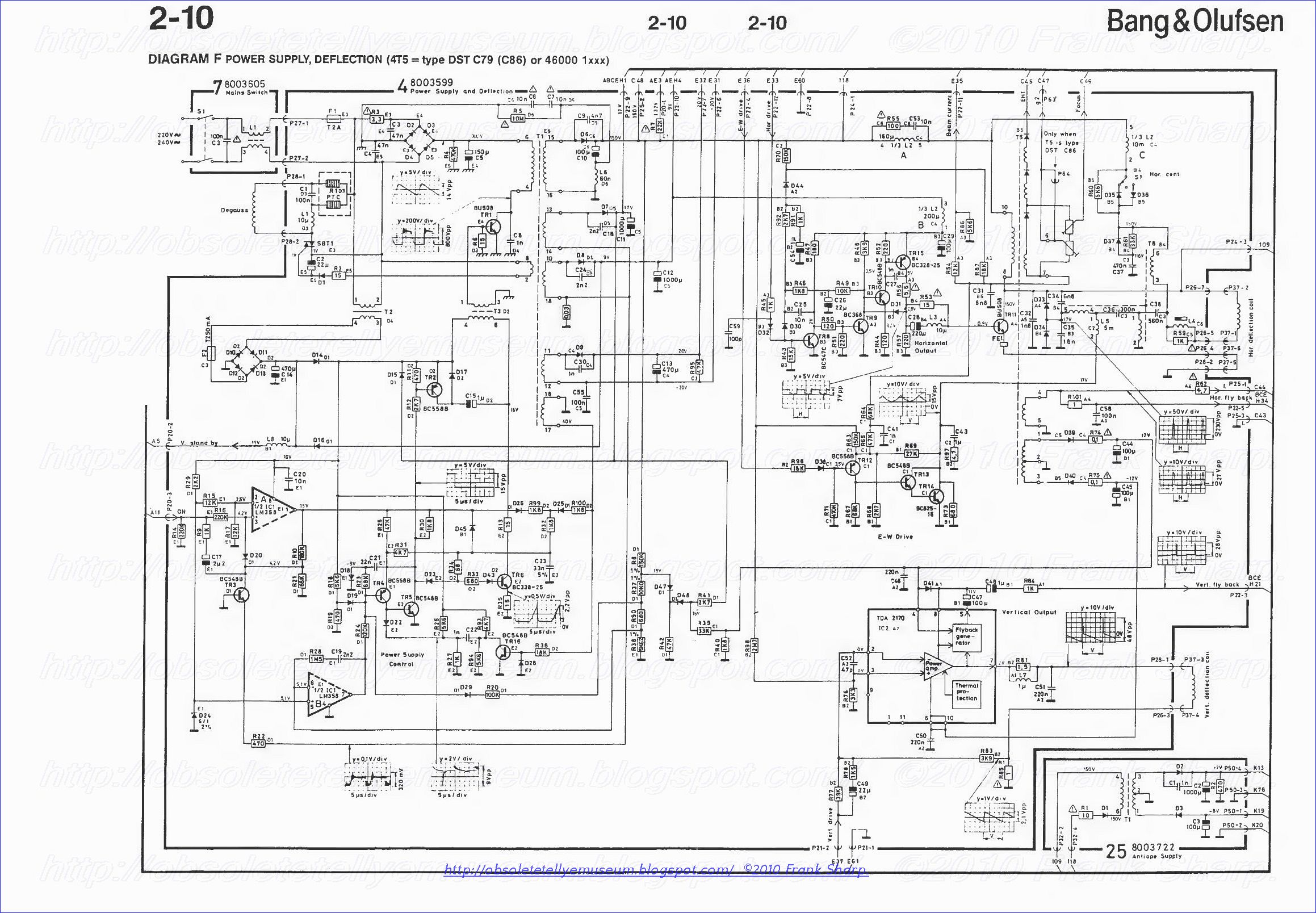
 Now take a brief look at some of the main circuitry used in these sets, starting with the chopper power supply - see Fig. 4. When going from standby to on the voltage at pin 22 of 1106 (see Fig. 2) goes low. Thus transistor 1TR25 switches off and pin 3 of the operational amplifier chip 4IC1 (Fig. 4) is positively biased from the 5V standby supply. The other input, pin 2, of this section of 41C1 is held at 2.5V by a zener diode stabilised feed. The output voltag.: at pin 1 of this chip therefore rises to 15V. As a result, 4C23 charges via 4D26 and 4R32, producing a positive going ramp which is fed via 4R31 to the emitter of 4TR4.
This transistor with 4TR5 form a regenerative switch. When 4TR4's emitter becomes positive with respect to its base it switches on, in turn switching 4TR5 on. 4C23 is then discharged via 4R34 and 4D23. The low voltage at the collector of 4TR5 when it switches on is fed back to the base of 4TR4 via 4C21 and 4R23. Thus 4TR4/5 are held on. As 4(21 discharges via 4R30 4TR4/5 unlatch. The sawtooth voltage thus developed drives 4TR6, the chopper driver transistor, which in turn drives the BU508 chopper transistor 4TR1 via 4T3. Note that 4T1/2/3 provide mains isolation. For timing and regulation, a negative -going pulse derived from winding 17-18 of the chopper transformer 4T1 is fed to the base of 4TR5 to control its switch -off time. The pulse obtained from 4T1 is an exact replica of 4TR1's collector waveform. It's clipped by 4R36, 4D28 and 4TR16 to produce a squarewave which is then differentiated by 4C22 and 4R27 to obtain the negative -going pulse that switches 4TR5 off. With 4TR4/5 off, 4C23 can once more begin to charge. The circuit is thus self -oscillating. In the TV mode, regulation is based on monitoring the 150V h.t. supply produced by 4D6/4C10. A tap on the potential divider 4R8/37/90/38 feeds pin 6 of 4IC1. The other input pin of this section of 4IC1 is held at 5.1V by the action of zener diode 4D24. The error output at pin 7 of 41C1 sets the bias at the base of 4TR4 and in consequence the point at which this transistor switches on. This regulation loop is kept stable by the action of 4C19 and 4R28. In the audio only mode the 150V rail is not loaded and cannot be used as the basis for regulation. In this mode the 17V supply is used as the basis for regulation, via 4D47 and 4D48.
During start-up 4C23 charges via 4D26 from the 17V standby supply. When running 4C23 charges via 4D25 from winding 17-18 of 4T1. Since the voltage here depends on the mains input, the charging of 4023 will vary as the mains supply varies, thus providing stabilisation against changes in the mains input. The regulation provided by this circuit is certainly impressive. The set will run on 60V (and that's with a 28in. c.r.t.!) and will start up with a 150V input. The line output stage is conventional, using a BU508 (4TR11) line output transistor, a diode -split line output transformer, and a diode modulator for EW correction.
The line output transformer provides the e.h.t., first anode, focus and c.r.t. heater voltages and also the +12V and -12V supplies used by the TDA2170 field output chip. The line drive signal is generated by a TDA1940 chip on panel 26/27 and is fed via 26/27TR3 to panel 4 where four transistors (4TR8/9/10/15) are used in the driver stage (no driver transformer). The purpose of 26/ 27-1123 is to act as a switch to remove the line drive in the audio only mode - this prevents e.h.t. generation. The field sync pulse output from the TDA1940 chip on panel 26/27 is passed to the colour decoder panel 21 and then back to 26/27TR21. This transistor's output is used to control the field oscillator, which consists of an LF353 dual operational amplifier chip (26/27IC6). Half of another dual operational amplifier chip, 26/27IC7 (LF358), acts as the field preamplifier which drives the TDA2170 on panel 4. The other half of 26/27IC7 providesEW drive. The TDA2170 drives the field scan coils directly - this is made possible by the energy efficient c.r.t. deflection system. The field oscillator runs at 471-1z to allow for graphics injection (e.g. tuning information) with no signal and thus no sync. The sync provides the extra three for 50Hz. Two TDA2040 chips on panel 26/27 provide 15W of audio output per channel at 81/ Each channel has a 4in. woofer and 2in. tweeter, with external speaker options.
BANG & OLUFSEN (B&O) BEOVISION LX 2502 Audio Output: The output from the audio detector is mono of course. It's split and fed via switching i.c.s 28IC1/2 then through 28IC7 to the dual volume/tone control circuits in 28IC8. Teletext subtitles can be recorded on these sets and also printed by a suitable printer (LX versions of course). As mentioned earlier, the L models are teletext adaptable.
This calls for removal of the display board - but hang on to this for diagnosis (it can prove a Bus 2 fault or teletext decoder fault). Note also that because of the power fail circuit these sets will not operate unless one or other of these boards is fitted. The on -screen display with text sets is provided by the text panel. Tuning is not by the well-known channel numbers (21- 68) but by frequency. Table 1 shows the equivalents. Despite the fact that the retail price of the LX2800 was over £1,000 these sets sold well in our area. They have since been replaced by the LX2502/2802 series (38XX type numbers) which have only two buses and built-in Link processing.
BANG & OLUFSEN (B&O) BEOVISION LX 2502 Stuck in Standby:
MY experience has been that faults are usually supply related or in the Bus 1 system. In either case the set will go into standby, as previously described. If you have a set that's stuck in standby and you don't know where to start, proceed as follows.
1 - Try to start the set in the audio only mode. If the set comes on you can rule out faults in the secondary supplies as these will all be up and running. It's likely that there's a Bus 1 fault.
The best policy is to switch off, short out the test link connected to pin 11 of 1106 and try the set in the TV mode again. This overrides bus error detection. The set will now more than likely start. If so check for data and clock signals on the appropriate lines. If absent check for d.c. pull-up. As previously mentioned absence of pull- up can be caused by open -circuit pull-up resistors or the protection zener diode being short-circuit. Another pos- sibility is excessive loading due to a faulty i.c. The bus lines should give a resistance reading to chassis of 3.5kf/. A quick check is to remove the 330f1 series resistors (see Fig. 2)
to see if this resistance returns. Also look for tuning. If there's none, suspect a fult in the tuning interface or memory.2 - If the set won't start in the audio only mode look for loading on the power supply, i.e. 4T1's secondaries, for example a short-circuit line output transistor. Such secon- dary loading is indicated by a noise in the chopper transformer. If there's no noise, suspect a mains input or control circuit fault. 4R3 could be open -circuit or 4TR1 may have failed. For repeated failure of 4TR1 check whether 4C15 (1µF) is open -circuit.
3 - Check for power failure detection at pin 1 of 1106. A high here indicates an overload on one of the 1.t. supplies. Once you've understood the basic operation of the chopper power supply and the bus control arrangements you should have no difficulty in repairing faults in these sets. Develop the correct technique for these areas and the rest is much the same as with anyone else's sets.
BANG & OLUFSEN (B&O) BEOVISION LX 2502 Fault List:
Here's a list of some of the faults I've had.
1 - A completely dead set (no standby light) is usually due to a burnt up mains switch. If the subpanel is damaged, as it usually is, the complete assembly (part number 8003605) should be replaced - this is done through the
flap in the bottom of the cabinet.
2 - The most common cause of a set being stuck in standby, again usually preceded by smoke, is an open - circuit surge limiter resistor (4R3, 3.3fl). A type with improved construction is now supplied.
3 - Reduced width and height has on a number of occasions been traced to the line flyback tuning capacitor 4C32 (1.5nF) being open -circuit.
4 - Stuck on standby, not a Bus 1 fault. The line output transistor 4TR11 short-circuit.
5 - A few lines of field foldover on the picture. Check the 0.1Si resistors 4R74 and 4R75 in series with the supplies to the TDA2170 field output chip.
6 - No control of a VCR via the Aux 2 socket when used in conjunction with a Beomaster 5500 and Master Control Panel 5500. Data reaching 1106 (MAB8461) but no output to the scart socket. Programming of options (datalink) correct but 1106 faulty.
7 - No picture when brought on from standby via the MCP 5500 with the above system. 211C3 (SAB3037) faulty.
8 - No line or field sync after a few seconds. 105 (TDA1940) on panel 26/27 faulty.
9 - Teletext not running, top line only displayed. Horizon- tal phase control 26/27R65 slightly off. As a final note, when removing the back cover it's not necessary to remove the screws completely - this saves losing them.
TDA2555 Dual TV sound demodulator circuits:
GENERAL DESCRIPTION
The circuits incorporate two FM demodulator systems to perform the demodulator functions required in a dual sound
carrier TV system for demodulating the sound carriers.
The difference between TDA2555 and TDA2557 is the number of stages of the limiting amplifier.
· Eight (TDA2555) or five (TDA2557) stage limiting amplifier
· Quadrature demodulator for FM detection
· De-emphasis stage
· Output amplifier
· Mute function for each FM demodulator.
TDA2545A Quasi-split-sound circuitGENERAL DESCRIPTION The TDA2545A is a monolithic integrated circuit for quasi-split-sound processing in television receivers. Features · 3-stage gain controlled i.f. amplifier · A.G.C. circuit · Reference amplifier and limiter amplifier for vision carrier (V.C.) processing · Linear multiplier for quadrature demodulation.
SAB3034 COMPUTER INTERFACE FOR TUNING AND CONTROL (CITAC)
GENERAL DESCRIPTION
The SAB3034 provides closed-loop digital tuning of TV receivers, with or without a.f.c., as required. lt
also controls up to 8 analogue functions, 4 general purpose I/O ports and 4 high-current outputs for
tuner band selection.
The IC is used in conjunction with a microcomputer from the MAB84OO family and is controlled via a two-wire, bidirectional I2 C bus.
Featu res
Combined analogue and digital circuitry minimizes the number of additional interfacing components
required
Frequency measurement with resolution of 50 KHz
Selectable prescaler divisor of 64 or 256
32 V tuning voltage amplifier
4 high-current outputs for direct band selection
8 static digital to analogue converters (DACSI for control of analogue functions
Four general purpose input/output (l/O) ports
Tuning with control of speed and direction
Tuning with or without a.f.c.
Single-pin, 4 MHZ on-chip oscillator
I2 C bus slave transceiver
FUNCTIONAL DESCRIPTION
The SAB3034 is a monolithic computer interface which provides tuning and control functions and
operates in conjunction with a microcomputer via an I2 C bus.
Tuning
This is performed using frequency-locked loop digital control. Data corresponding to the required tuner
frequency is stored in a 15-bit frequency buffer. The actual tuner frequency, divided by a factor of 256
(or by 64) by a prescaler, is applied via a gate to a 15-bit frequency counter. This input (FDIV) is
measured over a period controlled by a time reference counter and is compared with the contents of the frequency buffer. The result of the comparison is used to control the tuning voltage so that the tuner frequency equals the contents of the frequency buffer multiplied by 50 kHz within a programmable tuning window (TUW).
The system cycles over a period of 6,4 ms (or 2,56 ms), controlled by the time reference counter which is clocked by an on-chip 4 lVlHz reference oscillator. Regulation of the tuning voltage is performed by a charge pump frequency-locked loop system. The charge IT flowing into the tuning voltage amplifier is controlled by the tuning counter, 3-bit DAC and the charge pump circuit. The charge IT is linear with the frequency deviation Af in steps of 50.
TDA2040 20W Hi-Fi AUDIO POWER AMPLIFIER:
DESCRIPTION
The TDA2040 is a monolithic integrated circuit in
Pentawatt[ package,intended for use as an audio
class AB amplifier. Typically it provides22W output
power (d = 0.5%) at Vs = 32V/4W . The TDA2040
provides high output current and has very low
harmonic and cross-over distortion. Further the
device incorporates a patented short circuit protection
system comprising an arrangement for automaticallylimiting
the dissipatedpowersoas to keep
the working point of the output transistors within
their safe operating area. A thermal shut-down
system is also included.
TDA1950, Line Circuits for TV Receivers (18-Pin Plastic Package)

These integrated circuits are advanced versions of the well-known types TDA1940, TDA1940F, TDA1950 and TDA1950F are identical
TBA940/950, TDA9400/9500 etc. integrated line oscillator circuits. except the following: at pin 2 the types having the suffix "F" supply ,
They comprise all stages for sync separation and line synchronisation horizontal output pulses of longer duration compared with the basic I
in TV receivers in one single silicon chip. Due to their high degree of types Integration, the number of external components is very small.
This integrated circuit contains the horizontal sweep generator (HO), the amplitude filter (AS), the sync-signal separating circuit (SA) and the frequency/phase comparator (FP). For the purpose of suppressing noise pulses which are caused via the operating voltage during the upper and the lower inversion point of the horizontal sweep generator (HO) which contains a single capacitor (C) and a first threshold stage circuit (SS1) with two fixed thresholds, there are provided a second and a third threshold stage circuit (SS2, SS3), to the inputs of which the sawtooth signal is applied, and with the thresholds thereof, approximately 2 μs prior to reaching the upper or the lower peak value of the sawtooth signal, are being passed through thereby. The output signal of the second threshold circuit (SS2) and the output signal of the third threshold stage circuit (SS3) which is applied via the pulse shaper circuit (IF), are superimposed linearly and, via the stopper circuit (blocking stage) (SP) serve to control the application of the composite video
signal (BAS) to the amplitude filter (AS), or else they are applied to a clamping circuit which serves to apply the operating points of the amplitude filter (AS) and/or of the sync-signal separating circuit (SA) to such a potential that these two stages, for the time duration of these output pulses, are prevented from operating. 1. An integrated circuit for color television receivers, comprising a voltage- or current-controlled horizontal sweep generator (HO), an amplitude filter (AS), a synchronizing-signal separating circuit (SA) and a frequency/phase comparator (FP) which serves to synchronize the horizontal sweep generator (HO), with said generator being a sawtooth generator containing a single capacitor (C) and a first threshold stage circuit (SS1) having two fixed thresholds, said integrated circuit further comprising:
a second and a third threshold stage circuit (SS2, SS3) each being supplied with the sawtooth signal on the input side, comprising each time one threshold which, approximately 2μs prior to the reaching of the upper or the lower peak value of the sawtooth signal, is being passed thereby;
a pulse shaper circuit (IF) coupled to the output of said third threshold stage circuit (SS3) which pulse shaper circuit reduces the duration of the output pulse thereof to about the duration of the output pulse of said second threshold stage circuit (SS2), and
a stopper circuit (blocking stage) (SP) coupled to the outputs of both said pulse shaper circuit (IF) and said second threshold stage circuit (SS2), said stopper circuit having a signal input to which there is applied a composite video signal (BAS) and a signal output which is coupled to the input of said amplitude filter (AS).
2. The invention of claim 1 wherein the outputs of both said pulse shaper circuit (IF) and said second threshold stage circuit (SS2) are coupled to a clamping circuit which applies the operating points of said amplitude filter (AS) and said sync-separating signal (SA) to such a potential that they are prevented from operating.
3. An integrated horizontal sweep circuit comprising:
a generator for generating a sawtooth signal;
an amplitude filter having an input for receiving a composite video signal and having an output;
a sync-signal separating circuit having an input coupled to said amplitude filter output and having an output;
a frequency/phase comparator having a first input coupled to said separating circuit output,
a second input receiving said sawtooth signal and an output for controlling said generator; and
a control circuit responsive to said sawtooth signal for inhibiting said composite video signal when said sawtooth signal is within predetermined signal level ranges about the upper and lower inversion points of said sawtooth signal.
4. An integrated circuit in accordance with claim 3 wherein:
said generator comprises a capacitor, circuit means for charging and discharging said capacitor, and a first threshold circuit controlling said circuit means in response to said sawtooth signal reaching a first level corresponding to said first inversion point and a second level corresponding to said second inversion point.
5. An i
ntegrated horizontal sweep circuit comprising: a sawtooth signal generator;
an amplitude filter having an input receiving a composite video signal and having an output;
a sync-signal separating circuit having an input coupled to said amplitude filter output and having an output;
a frequency/phase comparator having a first input coupled to said separating circuit output, a second input receiving said sawtooth signal and an output for controlling said generator; and
a control circuit responsive to said sawtooth signal for inhibiting operation of said amplitude filter and/or said sync-signal separating circuit when said sawtooth signal is within predetermined signal level ranges about the upper and lower inversion point of said sawtooth signal.
6. An integrated circuit in accordance with claim 5 wherein:
said generator comprises a capacitor, circuit means for charging and discharging said capacitor and a first threshold circuit controlling said circuit means in response to said sawtooth signal reaching a first level corresponding to said first inversion point and a second level corresponding to said second inversion point.
The invention relates to an integrated circuit for (color) television receivers, comprising a voltage- or current-controlled horizontal-sweep generator, an amplitude filter, a synchronizing signal separating circuit (sync-separator) and a frequency/phase comparator which serves to synchronize the horizontal sweep generator which is a sawtooth generator consisting of a single capacitor and of a first threshold stage having two fixed switching thresholds, cf. preamble of the patent claim. Such types of integrated circuits, for example, are known from the technical journal "Elektronik aktuell", 1976, No. 2, pp. 7 to 14 where they are referred to as TDA 9400 and TDA 9500.
Especially on account of the fact that the amplitude filter as well as the horizontal sweep generator in the form of the aforementioned sawtooth generator, are integrated on a single semiconductor body, it is likely that noise interference pulses coming from the individual stages, and via the supply voltage line, may have a disturbing influence upon the horizontal sweep generator, i.e. upon the threshold stage thereof, in such a way that either the lower or the upper or successively both switching thresholds are exceeded before the time by the voltage at the capacitor, owing to the noise superposition, so that the generator will show to have a "wrong" frequency or phase position. This frequency/phase variation, of course, is compensated for by the circuit, with the aid of the synchronzing pulses, but only in such a way that the noise effect remains visible in the television picture.
SUMMARY OF THE INVENTION
The invention is characterized in the claim is aimed at overcoming this drawback by solving the problem of designing an integrated circuit of the type described in greater detail hereinbefore, in such a way that noise pulses acting upon the capacitor voltage or the internal reference voltages for the switching thresholds (see below) in the proximity of the two switching thresholds, are prevented from having the described disadvantageous effect. Accordingly, an advantage of the invention results directly from solving the given problem.
Other objects, features and advantages of the present invention will become more fully apparent from the following detailed description of the preferred embodiment, the appended claims and the accompanying drawing in which:
BRIEF DESCRIPTION OF THE INVENTION
The invention will now be described in greater detail with reference to the accompanying drawing. This drawing, in the form of a schematical circuit diagram, shows the construction of an integrated circuit according to the invention.
DETAILED DESCRIPTION OF THE INVENTION
The horizontal sweep generator HO comprises the capacitor C as connected to the zero point of the circuit, and which is charged and discharged via the two shown constant current sources CS1 and CS2, thus causing the intended sawtooth voltage to appear thereat. Moreover, the horizontal sweep generator HO comprises the first threshold stage circuit SS1, having an upper and a lower threshold. As soon as the capacitor voltage exceeds one of the thresholds, the first threshold stage circuit SS1 switches over to the other threshold. The two thresholds are defined by the voltage divider P as connected to the operating voltage U, and in which the corresponding threshold inputs are connected to corresponding tapping points. The output of the threshold stage circuit SS1 controls the electronic switch S, so that the constant current source CS2 as connected thereto, is either disconnected from or connected to the zero point of the circuit. Accordingly, in the disconnected state, the capacitor C is charged via the constant current source CS1 arranged in series therewith while in the connected state the capacitor C is discharged across the aforementioned constant current source CS2 arranged in parallel therewith, if, as a matter of fact, the current of the constant current source CS1 arranged in series with the capacitor C, is smaller than that of the parallel-arranged constant current source CS2.
Now, for the purpose of avoiding the aforementioned drawbacks, there is provided a second and a third threshold stage circuit SS2 and SS3, respectively, as well as the pulse shaper circuit IF. To the respective input of the two threshold stage circuits SS2, SS3, there is applied the capacitor voltage, in the form of the sawtooth signal, and these stages have a threshold voltage which, approximately 2 μs prior to the reaching of the upper or the lower peak value of the sawtooth voltage, is being passed thereby. This means to imply that the threshold voltage of the second threshold stage circuit SS2 is somewhat lower than the voltage of the upper threshold of the first threshold stage circuit SS1, and that the threshold voltage of the third threshold stage circuit SS3 is somewhat higher than the voltage of the lower threshold of the first threshold stage circuit SS1. The two thresholds of the threshold stage circuits SS2, SS3 can thus be realized in a simple way by providing further tapping points at the voltage divider P, as is shown in the accompanying drawing. Thus, the second threshold stage circuit SS2 is provided for at a voltage divider tapping point below the tapping point chosen for the upper threshold, and the tapping point for the third threshold stage circuit SS3 is provided for above the tapping point which has been chosen for the lower threshold of the first threshold stage circuit SS1.
Since, within the area of the lower inversion point of the sawtooth signal there results an excessively wide output pulse of the third threshold stage circuit SS3, the pulse shaper circuit IF is arranged subsequently thereto, for reducing the duration of the output pulse as applied to its input, to about the duration of the output pulse of the second threshold stage circuit SS2. This pulse shaper circuit IF, for example, may be realized by a monoflop, in particular by a digital monoflop (=monostable circuit).
The output pulses of the second threshold stage circuit SS2 and of the pulse shaper circuit IF are then super-positioned linearly, with this being denoted in the drawing by a simple interconnection of the two respective lines. The combined signal is applied to the input of the stopper circuit (blocking stage) SP, to the signal input of which there is fed the composite video signal BAS, and the output thereof controls both the amplitude filter AS and the synchronizing signal separating circuit SA.
The combined signal may also be used to control a clamping circuit applying the operating points of the amplitude filter AS and/or of the sync-signal-separating circuit SA to such a potential which prevents it from operating.
If now the sawtooth signal reaches the range of its upper or its lower inversion point, the composite video signal BAS is not applied to either the amplitude filter AS or the sync-signal separating circuit SA, so that shortly before and shortly after the inversion points, signals are prevented from being processed in the two stages AS, SA. This, in turn, has the consequence that during these times noise pulses are prevented from superimposing upon the operating voltage U, so that there is also prevented an unintended triggering of the first threshold stage circuit SS1.
Moreover, it is still shown in the drawing that the amplitude filter AS, the sync-signal separating circuit SA and the frequency/phase comparator FP are arranged in series in terms of signal flow, with the latter, in addition, receiving the sawtooth signal, and with the output signal thereof acting upon the two current sources in a regulating sense. In the drawing, this is indicated by the setting arrows at the two current sources.
While the present invention has been disclosed in connection with the preferred embodiment thereof, it should be understood that there may be other embodiments which fall within the spirit and scope of the invention as defined by the following claims.
- VIDEO CHROMA PROCESSING WITH TDA3300 (MOTOROLA)

TDA3300 3301 TV COLOR PROCESSOR
This device will accept a PAL or NTSC composite video signal and output the
three color signals, needing only a simple driver amplifier to interface to the pic-
ture tube. The provision of high bandwidth on-screen display inputs makes it
suitable for text display, TV games, cameras, etc. The TDA3301 B has user con»
trol laws, and also a phase shift control which operates in PAL, as well as NTSC.
0 Automatic Black Level Setup
0 Beam Current Limiting
0 Uses Inexpensive 4.43 MHZ to 3.58 MHz Crystal
0 No Oscillator Adjustment Required
0 Three OSD Inputs Plus Fast Blanking Input
0 Four DC, High Impedance User Controls
0 lnterlaces with TDA33030B SECAM Adaptor
0 Single 12 V Supply
0 Low Dissipation, Typically 600 mW
The brilliance control operates by adding a pedestal to the output
signals. The amplitude of the pedestal is controlled by Pin 30.
During CRT beam current sampling a standard pedestal is
substituted, its value being equivalent tothe value given by V30 Nom
Brightness at black level with V30 Nom is given by the sum of three gun
currents at the sampling level, i.e. 3x20 |.1A with 100 k reference
resistors on Pins 16, 19, and 22.
During picture blanking the brilliance pedestal is zero; therefore, the
output voltage during blanking is always the minimum brilliance black
level (Note: Signal channels are also gain blanked).
Chrominance Decoder
The chrominance decoder section of the TDA3301 B
consists of the following blocks:
Phase-locked reference oscillator;
Phase-locked 90 degree servo loop;
U and V axis decoders
ACC detector and identification detector; .
Identification circuits and PAL bistable; .
Color difference filters and matrixes with fast blanking
Circuits.
The major design considerations apart from optimum
performance were:
o A minimum number of factory adjustments,
o A minimum number of external components,
0 Compatibility with SECAM adapter TDA3030B,
0 Low dissipation,
0 Use of a standard 4.433618 Mhz crystal rather
than a 2.0 fc crystal with a divider.
The crystal VCO is of the phase shift variety in which the
frequency is controlled by varying the phase of the feedback.
A great deal of care was taken to ensure that the oscillator loop
gain and the crystal loading impedance were held constant in
order to ensure that the circuit functions well with low gradecrystal (crystals having high magnitude spurious responses
can cause bad phase jitter). lt is also necessary to ensure that
the gain at third harmonic is low enough to ensure absence of
oscillation at this frequency.
It can be seen that the
necessary 1 45°C phase shift is obtained by variable addition
ol two currents I1 and I2 which are then fed into the load
resistance of the crystal tuned circuit R1. Feedback is taken
from the crystal load capacitance which gives a voltage of VF
lagging the crystal current by 90°.
The RC network in the T1 collector causes I1 to lag the
collector current of T1 by 45°.
For SECAM operation, the currents I1 and I2 are added
together in a fixed ratio giving a frequency close to nominal.
When decoding PAL there are two departures from normal
chroma reference regeneration practice:
a) The loop is locked to the burst entering from the PAL
delay line matrix U channel and hence there is no
alternating component. A small improvement in signal
noise ratio is gained but more important is that the loop
filter is not compromised by the 7.8 kHz component
normally required at this point for PAL identification
b) The H/2 switching of the oscillator phase is carried out
before the phase detector. This implies any error signal
from the phase detector is a signal at 7.8 kHz and not dc.
A commutator at the phase detector output also driven
from the PAL bistable coverts this ac signal to a dc prior
to the loop filter. The purpose ot this is that constant
offsets in the phase detector are converted by the
commutator to a signal at 7.8 kHz which is integrated to
zero and does not give a phase error.
When used for decoding NTSC the bistable is inhibited, and
slightly less accurate phasing is achieved; however, as a hue
control is used on NTSC this cannot be considered to be a
serious disadvantage.
90° Reference Generation
To generate the U axis reference a variable all-pass network
is utilized in a servo loop. The output of the all-pass network
is compared with the oscillator output with a phase detector of
which the output is filtered and corrects the operating point of
the variable all»pass network .
As with the reference loop the oscillator signal is taken after
the H/2 phase switch and a commutator inserted before the
filter so that constant phase detector errors are cancelled.
For SECAM operation the loop filter is grounded causing
near zero phase shift so that the two synchronous detectors
work in phase and not in quadralure.
The use of a 4.4 MHz oscillator and a servo loop to generate
the required 90° reference signal allows the use of a standard,
high volume, low cost crystal and gives an extremely accurate
90° which may be easily switched to 0° for decoding AM
SECAM generated by the TDA3030B adapter.
ACC and Identification Detectors
During burst gate time the output components of the U and
also the V demodulators are steered into PNP emitters. One
collector current of each PNP pair is mirrored and balanced
against its twin giving push-pull current sources for driving the
ACC and the identification filter capacitors.
The identification detector
is given an internal offset bymaking the NPN current mirror emitter resistors unequal. The
resistors are offset by 5% such that the identification detector
pulls up on its filter capacitor with zero signal.
Identification
See Figure 11 for definitions.
Monochrome I1 > I2
PAL ldent. OK I1 < lg
PAL ldent_ X l1 > I2
NTSC I3 > I2
Only for correctly identified PAL signal is the capacitor
voltage held low since I2 is then greater than I1.
For monochrome and incorrectly identified PAL signals l1>l2
hence voltage VC rises with each burst gate pulse.
When V,ef1 is exceeded by 0.7 V Latch 1 is made to conduct
which increases the rate of voltage rise on C. Maximum
current is limited by R1.
When Vref2 is exceeded by 0.7 V then Latch 2 is made to
conduct until C is completely discharged and the current drops
to a value insufficient to hold on Latch 2.
As Latch 2 turns on Latch 1 must turn off.
Latch 2 turning on gives extra trigger pulse to bistable to
correct identification.
The inhibit line on Latch 2 restricts its conduction to alternate
lines as controlled by the bistable. This function allows the
SECAM switching line to inhibit the bistable operation by firing
Latch 2 in the correct phase for SECAM. For NTSC, Latch 2
is fired by a current injected on Pin 6.
lf the voltage on C is greater than 1.4 V, then the saturation
is held down. Only for SECAM/NTSC with Latch 2 on, or
correctly identified PAL, can the saturation control be
anywhere but minimum.
NTSC Switch
NTSC operation is selected when current (I3) is injected into
Pin 6. On the TDA33O1 B this current must be derived
externally by connecting Pin 6 to +12 V via a 27 k resistor (as
on TDA33OOB). For normal PAL operation Pin 40 should be
connected to +12 V and Pin 6 to the filter capacitor.
4 Color Difference Matrixing, Color Killing,
and Chroma Blanking
During picture time the two demodulators feed simple RC
filters with emitter follower outputs. Color killing and blanking
is performed by lifting these outputs to a voltage above the
maximum value that the color difference signal could supply.
The color difference matrixing is performed by two
differential amplifiers, each with one side split to give the
correct values of the -(B-Y) and -(Ft-Y) signals. These are
added to give the (G-Y) signal.
The three color difference signals are then taken to the
virtual grounds of the video output stages together with
luminance signal.
Sandcastle Selection
The TDA3301B may be used with a two level sandcastle
and a separate frame pulse to Pin 28, or with only a three level
(super) sandcastle. In the latter case, a resistor of 1.0 MQ is
necessary from + 12 V to Pin 28 and a 70 pF capacitor from
Pin 28 to ground.
Timing Counter for Sample Control
In order t
o control beam current sampling at the beginning
of each frame scan, two edge triggered flip-flops are used.
The output K ofthe first flip-flop A is used to clock the second
tlip-flop B. Clocking of A by the burst gate is inhibited by a count
of A.B.
The count sequence can only be initiated by the trailing
edge of the frame pulse. ln order to provide control signals for:
Luma/Chroma blanking
Beam current sampling
On-screen display blanking
Brilliance control
The appropriate flip-flop outputs ar matrixed with sandcastle
and frame signals by an emitter-follower matrix.
Video Output Sections
Each video output stage consists of a feedback amplifier in A further drive current is used to control the DC operating
which the input signal is a current drive to the virtual earth from point; this is derived from the sample and hold stage which
the luminance, color difference and on-screen display stages. samples the beam current after frame flyback.
TDA2170 TV VERTICAL DEFLECTION OUTPUT CIRCUIT:
DESCRIPTION
The TDA2170 is a monolithic integrated circuit in
11-lead Multiwatt) package. It is a high efficiency
power booster for direct driving of vertical windings
of TV yokes. It is intended for use in Colour are B
& Wtelevision receivers as well as in monitors and
displays.
The functions incorporated are :
.POWERAMPLIFIER
.FLYBACKGENERATOR
.REFERENCE VOLTAGE
.THERMAL PROTECTION
MOUNTING INSTRUCTIONS
The power dissipated in the circuit must be removed
by adding an external heatsink.
Thanks to the MULTIWATT) package attaching
the heatsink is very simple, a screw or a compression
spring (clip) being sufficient. Between the
heatsinkand the packageit is better to insert a layer
of silicon grease, to optimize the thermal contact ;
no electrical isolation is needed between the two
surfaces.


Dear Frank, we have a 2802 with a problem in the vertical deflection, because there is only a horizontal line on the screen appearing when turned on. Did you come across such a fault before? Is there any advise where to check? Common failure? Thanks!
ReplyDeleteI had this problem with my LX2800. I fixed it by replacing capacitors C46, C47 and C48 on the Power supply / Deflection board (from the back, it's the PCB on the right hand side, and the caps are in the top left hand corner on the inside of the PCB). I used low ESR 100uf 63V capacitors.
DeleteEasy fix.
ReplyDelete- check supply at TDA2170 IC.
- CHECK SOLDER JOINTS AS THESE TVS MAY SUFFER OF BAD JOINTS ALLA AROUND BOARDS.
- replace ic TDA2170 TV VERTICAL DEFLECTION OUTPUT CIRCUIT IF NECESSARY AND IF THE SUPPLY SAFETY RESISTORS ARE BLOWN.
- MANDATORY REPLACEMENT OF ALL ELECTROLYTIC CAPACITORS IN THE VERTICAL DEFLECTION SECTION IF TDA2170 HAS TO BE REPLACED. *DO IT BEFORE REPLACING THE TDA2170
- IF YOU ARE NOT PREPARED WITH NECESSARY KNOWLEDGE AND TRAINING FOR SUCH REPAIR LEAVE IT TO A PROFESSIONAL, TO AVOID FURTHER DAMAGE BEYOND REPAIR
Thank you so much for your help. We have replaced the capacitors and replaced the TDA2170. It now works great again. Easy fix if you have the right info!
ReplyDeleteThanks for all the info about this TV. I have just got a faulty lx2802 that I'm fixing up. Fingers crossed I can fix it.
ReplyDelete