


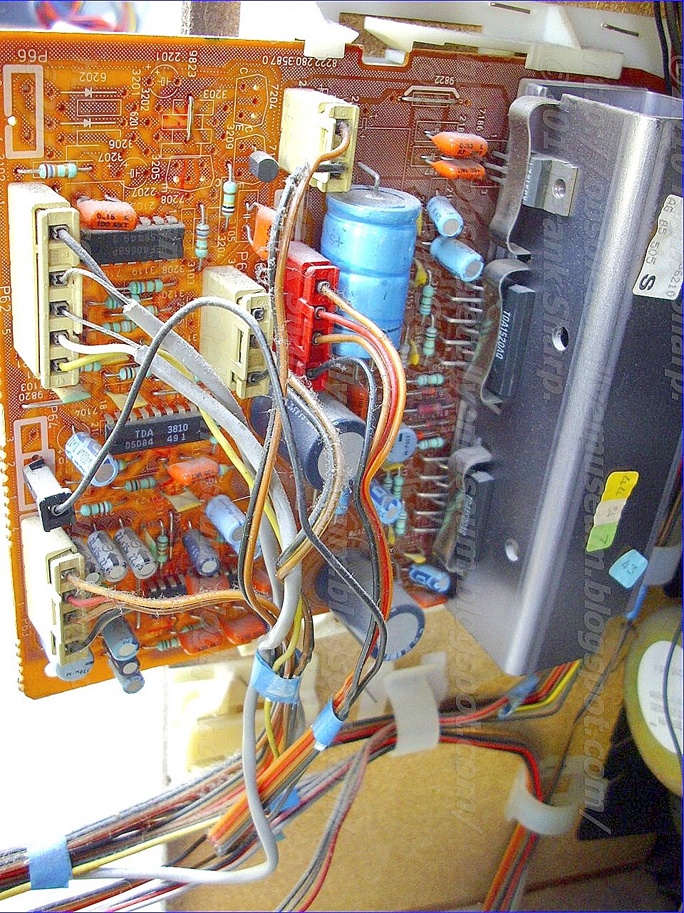


- Deflection Board on the right called large signal board. Line deflection output (BU508A) + EHT, E/W
Correction, FRAME Deflection Output with IC TDA3650 (PHILIPS)
- Signal processing board + Tuning control drive TRD (Tuning Remote Digital)
Chrominance + Luminance with TDA3561A,
GENERAL DESCRIPTION
The TDA3561A is a decoder for the PAL colour television standard. It combines all functions required for the identification

and demodulation of PAL signals. Furthermore it contains a luminance amplifier, an RGB-matrix and amplifier. These
amplifiers supply output signals up to 5 V peak-to-peak (picture information) enabling direct drive of the discrete output
stages. The circuit also contains separate inputs for data insertion, analogue as well as digital, which can be used for
text display systems (e.g. (Teletext/broadcast antiope), channel number display, etc. Additional to the TDA3560, the
circuit includes the following features:
· The peak white limiter is only active during the time that the 9,3 V level at the output is exceeded. The start of the
limiting function is delayed by one line period. This avoids peak white limiting by test patterns which have abrupt
transitions from colour to white signals.
· The brightness control is obtained by inserting a variable pulse in the luminance channel. Therefore the ratio of
brightness variation and signal amplitude at the three outputs will be identical and independent of the difference in gain
of the three channels. Thus discolouring due to adjustment of contrast and brightness is avoided.
· Improved suppression of the internal RGB signals when the device is switched to external signals, and vice versa.
· Non-synchronized external RGB signals do not disturb the black level of the internal signals.
· Improved suppression of the residual 4,4 MHz signal in the RGB output stages.
· Cascoded stages in the demodulators and burst phase detector minimize the radiation of the colour demodulator
inputs.
· High current capability of the RGB outputs and the chrominance output.
Synchronization With TDA3576B.12V 70mA sync combination with transmitter identification and vertical 625 divider system
PHILIPS TDA3576B SYNC COMBINATION WITH TRANSMITTER IDENTIFICATION
AND VERTICAL 625 DIVIDER SYSTEM.
GENERAL DESCRIPTION
The TDA3576B is a monolithic integrated circuit for use in colour television receivers. The circuit is
optimized for a horizontal and vertical frequency ratio of 625.
Features
• Horizontal sync separator (including noise inverter) with sliding bias such that the sync pulse is
always sliced between top sync level and blanking level
• Phase detector which compares the horizontal sync pulse with the oscillator voltage; this phase
detector is gated
• Phase detector which compares the horizontal flyback pulse with the oscillator voltage
• Horizontal oscillator (31,25 kHz)
• Time constant switching of the first control loop (short time constant during catching and reception
of VCR signals)
• Burst key pulse generator (sandcastle pulse with three levels)
• Very stable automatic vertical synchronization due to the 625 divider system, without delay after
channel change
• Vertical sync pulse separator
• Three voltage level sensor on coincidence detector circuit output
• Video transmitter identification circuit for sound muting and search tuning systems
• Inhibit of vertical sync pulse when no video transmitter is detected.
FUNCTIONAL DESCRIPTION
The video input voltage to drive the sync separator must have negative-going sync, which can be
obtained from synchronous demodulators such as TDA2540 and TDA2541.
The slicing level of the sync separator is determined by the value of the resistor between pins 6 and 7. A
4, 7 kr2 resistor provides a slicing level midway between the top sync level and the blanking level. Thus
the slicing level is independent of the amplitude of the sync pulse input at pin 5.
The nominal top sync level at pin 5 is 3 V, and the amplitude selective noise inverter is activated at
0,7 V.
To
obtain good stability the circuit contains three control loops. In the
first loop the phase of the horizontal sync pulse is compared with a
reference output pulse from the horizontal oscillator. In the second
loop the phase of the flyback pulse is compared with the same reference
output pulse. The first loop is designed for good noise immunity and the
second loop has a fast time constant to compensate quickly for storage
variations of the output stage. The second loop also generates a gating
signal of about 5,5 μs for use in the transmitter identification
circuit. The third control loop generates a second gating signal which
is used in the first phase detector. The pulse width is typically 14 μs.
For a short catching time the output current of the first phase
detector is not gated but is increased by 5 times during catching. This
is caused by the voltage of the coincidence detector at pin 9. For VCR
playback conditions the first control loop must be forced to a fast time
constant, this is achieved by applying an external voltage of~ 2,7 V to
pin 9.
The free running output frequency of the horizontal
oscillator is 31,25 kHz. The vertical frequency output is obtained by
dividing this double horizontal frequency by 625. The double horizontal
fre- quency is fed via a binary divider to provide the normal 15,625 kHz
horizontal output to pin 11. The sandcastle pulse is generated at pin 2
and has three levels. The burst key pulse is of short duration,
typically 4 μs, with an amplitude of 10 Vandis the highest level. The
second level has a pulse duration equal to the horizontal flyback pulse
with an amplitude of 4,5 Vandis used for horizontal blanking. The third
level, amplitude 2,5 V, is used for vertical blanking and has a pulse
duration of 1,34 ms. The last pulse is internal Iv generated by the
divider circuit and is only available when a standard video input signal
is received. An external vertical blanking pulse can be added to this
pin via a suitable series resistor. This pulse will be automatically
clamped to 2,5 V.
The automatic vertical sync block contains the following:
• 625 divider
• In/out-sync detector
• Direct/indirect sync switch
• Identification circuit
It
is fed by a signal obtained by integration of the composite video
signal and an internally generated, clipped video signal. The vertical
sync pulse is sliced out of this integrated signal by an automatically
biased clipper. The video part of the signal helps to build up a
vertical sync when heavy negative-going reflections (mountains) distort
the video signal. The in/out sync-detector considers a signal
out-of-sync when fourteen or more successive incoming vertical sync
pulses are not in phase with a reference signal from the 625 divider.
Therefore a distorted vertical sync signal needs only one
out-of-fourteen pulses to be in phase to keep the system in sync. When
the fifteenth successive out-of-sync pulse is detected, the
direct/indirect sync switch is activated to feed the vertical sync
signal directly out of the block at pin 3 (direct sync vertical output).
At the same time the 625 divider is reset by one of the sync pulses.
After the reset pulse, if the 7th sliced vertical sync pulse coincides
with a 625 divider window, the sync output pulse is presenteu again by
the divider system and switch-over to indirect mode occurs. In the
direct mode, every 7th non-coinciding sliced vertical sync pulse will
reset the counter. A non- standard video signal will result in
continuous reset pulses and the direct/indirect switch will remain in
the direct position.
To avoid delay in vertical synchronization, caused by waiting time of the divider circuit after channel
change or an unsynchronized camera change in the studio, information is fed from the horizontal
coincidence detector to the automatic switch for the vertical sync pulse. The loss of horizontal
synchronization sets the automatic switch to direct vertical sync.
When an external voltage between 2,7 V and 8,2 V is applied via pin 9 to the coincidence detector, the
horizontal phase detector is switched to a short time constant and the automatic switch to direct
vertical sync. A voltage level on pin 9 between 9,2 V and 12 V switches the horizontal phase detector
to a short time constant, without affecting the indirect/direct vertical sync system which remains
operational. Thus when standard signals are received vertical sync pulses are generated by the divider
system.
To avoid disturbance of the horizontal phase detector by the vertical sync pulse the 625 divider system
generates an anti-top-flutter pulse. This pulse is applied to the phase 1 detector when a standard video
signal is received. The anti-top-flutter pulse is also active for standard VCR signal conditions, voltage at
pin 9;;. 9,2 V.
The video transmitter identification circuit detects when a sync pulse occurs during the internal 5,5 μs
gating pulse. This indicates the presence of a video transmitter and results in the capacitor connected
to pin 1 being charged to 8,4 V. When no sync pulse is present the capacitor discharges to< 1 V. The
voltage at pin 1 is compared with an internal d.c. voltage. The identification output at pin 18 is active
when pin 1 is.;; 1,5 V (no video transmitter) and inactive (high impedance) when pin 1 is> 3,5 V,
this information can be used for search tuning.
The vertical sync output pulse at pin 3 is inhibited when no video transmitter is identified, which
prevents interference or noise affecting the frequency of the vertical output stage. This results in a
vertical stable picture, plus vertical stable position information for tuning systems.
RATINGS
Limiting values in accordance with the Absolute Maximum System (IEC 134)
Supply voltage (pin 17) Vp = V17-10 max. 13,2 v
Total power dissipation max. 1200 mW
Storage temperature range -55 to + 125 oc
Operating ambient temperature range -25 to +65 oc
THERMAL RESISTANCE From junction to ambient (in free air) Rthj-a 50 K/W
The function is described against the corresponding pin number.
1. Video transmitter identification
A 47 nF capacitor must be connected to this pin. It charges to a level of 8 V when a sync pulse is
detected, and discharges to a level of< 1 V when no sync pulse is detected.
2. Sandcastle output pulse
This output has three levels. The first and highest level (10 V) is the burst key pulse with a typical
duration of 4,0 μs. The second level, for the horizontal blanking, is typically 4,5 V with a pulse duration
equal to the horizontal flyback pulse. For the third level an external vertical flyback pulse must be
applied to this pin. This pulse will be clamped to 2,5 V by an internal clamping circuit. The input
current is typically 2 mA.
3. Vertical output pulse
This pulse is obtained from the 625 divider circuit when standard input signals are received or from the
sync separator when the signals are non-standard. The pulse is inhibited when no video transmitter is
detected. Both pulses have good stability and accuracy and are used to trigger the vertical oscillator.
4. Vertical sync pulse integrator biasing network
The vertical sync pulse is obtained by integrating the composite sync signal in an internal RC-network. An
external capacitor of 10 μF is required for biasing the vertical sync separator, this provides the vertical
sync output pulse with a delay of 37 μs. This value can be changed by an external resistor. A resistor of
470 kn between pin 3 and +12 V gives a delay of 45 μs.
5. Video input
The video input signal must have negative-going sync pulses. The top-sync level can vary between 1 V
and 3,5 V without affecting the sync separator operation. The slicing level is fixed at 50% for the
sync pulse amplitude range 0,1 to 1 V which provides good sync separation down to pulses with an
amplitude of 100 mV peak-to-peak. The slicing level is increased for sync pulses in excess of 1 V
peak-to-peak. The noise gate is activated at an input level< 1 V, thus when noise gating is required the
top sync level should be close to the minimum level of 1 V.
6. Sync separator slicing level output
The sync separator slicing level is determined on this pin. A slicing level of 50% is obtained by
comparing this level with the black level of the video signal, which is detected at pin 7.
7. Black level detector output
The black level of the input signal is detected on this pin. This is required to obtain good sync
separator operation. A 22 μF capacitor in series with a resistor of 82 n must be connected to this pin.
A 4,7 kU resistor connected between pins 6 and 7 results in a slicing level of 50%.
8. Horizontal phase detector output and control oscillator input
The flywheel filter must be connected to this pin. Typical values for the components are a capacitor of
100 nF in parallel with an RC-network of 1 kr2 and 10 μF. Furthermore, a resistor of 270 kH should
be connected between pins 8 and 13 to limit the free running frequency drift.
The output current of the phase detector depends on the condition of the coincidence detector. The
output current is high when the oscillator is out-of-sync. The result is a large catching range, and the
phase detector not gated. The output current is low when the oscillator is synchronized and the phase
detector is gated; this provides good noise immunity.
9. Coincidence detector output
A 1 μF capacitor must be connected to this pin. The output voltage depends on the oscillator condition
(synchronized or not) and on the video input signal. The following output voltages can occur:
• when in-sync
1,3 V
• when out-of-sync
2,7 V
• during noise at the input
2, 1 V
There are two switching levels at pin 9. At the first switching level when the output voltage is< 2, 1 V,
the phase detector output is low and the gating of the phase detector is switched on. When the output
voltage is> 2,7 V, the output current of the phase detector is high and the gating of the phase detector
is switched off. The result is a large catching range and a high dynamic steepness of the PLL. At the
second switching level when the output voltage is> 9,2 V the sync system is switched to a short time
constant while the indirect/direct vertical sync system remains fully operational. This condition is
suitable for VCR application.
10. Negative supply (ground)
11. Horizontal sync pulse output
This is an open collector output. The collector resistor mus be chosen such that sufficient current is
supplied
to the driver stage. The maximum current is 60 mA. The circuit is
designed such that the horizontal output transistor cannot be switched
on during flyback, but is switched on directly after flyback.
12. Control voltage second loop
This voltage controls the output pulse at pin 11 (positive-going edge). The capacitor connected to this
pin must have a minimum value of 6,8 nF. A higher value decreases the dynamic-loop gain in the second
control loop. When a high dynamic-loop gain is not required a capacitor value of 100 nF is recommended.
Horizontal shift is possible by applying an external current to pin 12.
13. Reference voltage control loops
The reference voltage must be decoupled by a capacitor of 10 μF.
14. Decoupling internal power supply
The IC has two power terminals. The main terminal (pin 17) supplies the output stages, the sync
separator and the divider circuit. The specially decoupled terminal (pin 14) supplies the horizontal
oscillator. The decoupling capacitor should be 22 μF.
15. Flyback input pulse
This pulse is required for the second phase control loop and for generating the horizontal blanking
pulse in the sandcastle output. The input current must be at least 0,2 mA and not exceed 3 mA.
16. RC-network horizontal oscillator
Stable components should be chosen for good frequency stability. For adjusting the frequency a part of
the total resistance must be variable. This part must be as small as possible, because of poor stability of
variable carbon resistors. The oscillator can be adjusted when pins 8 and 13 are short circuited (see Fig. 3).
17. Positive supply
The supply voltage may vary between 10,5 and 13,2 V. The current-draw is typ. 70 mA and the range is
50 to 85 mA.
·
18. Video transmitter identification output
This is an emitter-follower output which will be inactive (high-impedance) when the level at pin 1 is
> 4 V (video transmitter detected). The output will be active high when the level at pin 1 is< 1,7 V
(no videotransmitterdetected).This feature can be used for search-tuning and sound-muting.


- Audio amplifier Unit.
- Power supply on the bottom of the cabinet (SOPS Supply).
PHILIPS 22CS5755 /08R CHOPIN CHASSIS K40 Switched-mode self oscillating supply voltage circuit:POWER SUPPLY (SOPS - Self Oscillating Power Supply)
A switched-mode self-oscillating supply voltage circuit for converting an input voltage into an output d.c. voltage which is substantially independent of variations of the input voltage and/or a load connected to the output voltage. The circuit comprises a first controllable switch connected in series with a transformer winding and a second controllable switch for turning-off the first switch. The conduction period of the first switch is controlled by means of a control voltage present on a control electrode of the second switch. The circuit can be switched-over to a stand-up state in which the energy supplied to the load is reduced to zero. A starting network is connected between the input voltage and the second switch so that the current therein flows through the second switch during the period of time this switch conducts and does not flow to the control electode of the first switch in the stand-by state.1. A switched-mode self-oscillating supply voltage circuit for converting an input voltage into an output d.c. voltage which is substantially independent of variations of the input voltage and/or of a load connected to the terminals of the output voltage, comprising a transformer having a primary and a feedback winding, a first controllable switch connected in series with the primary winding, the series arrangement thus formed being coupled between terminals for the input voltage, a second controllable switch coupled via a turn-off capacitor to the control electrode of the first switch to turn it off, means coupling the feedback winding to said control electrode, a transformer winding being coupled via a rectifier to an output capacitor having terminals which supply the output voltage, an output voltage-dependent control voltage being present on a control electrode of the second switch for controlling the conduction period of the first switch, the circuit being switchable between an operating state and a stand-by state in which relative to the operating state the supply energy supplied to the load is considerably reduced, a starting network connected to a terminal for the input voltage, means for adjusting the control voltage in the stand-by state to a value at which the first controllable switch is cut-off, a connection which carries current during the conduction period for the second controllable switch being provided between the starting network and said second switch, and means providing a connection between the starting network and the control electrode of the first switch, which connection does not carry current in the stand-by state.
2. A supply voltage circuit as claimed in claim 1, further comprising a resistor included between the connection of the starting network to the second switch and a turn-off capacitor present in the connection to the control electrode of the first switch.
3. A supply voltage circuit as claimed in claim 2, characterized in that the second controllable switch comprises a thyristor having a main current path included in the control electrode connection of the first controllable switch, said thyristor having a first control gate electrode for adjusting the turn-off instant of the first switch and a second control electrode to which the starting network and the resistor are connected.
4. A supply voltage circuit as claimed in claim 1, characterized in that a resistor is included in the connection to the control electrode of the second controllable switch so that a current flows through said resistor in the stand-by state of a value sufficient to cut-off the first controllable switch.
The invention relates to a switched-mode self-oscillating supply voltage circuit for converting an input voltage into an output d.c. voltage which is substantially independent of variations of the input voltage and/or of a load connected to the terminals of the output voltage. This circuit comprises a transformer having a primary and a feedback winding and a first controllable switch arranged in series with the primary winding. The series arrangement thus formed is coupled between the terminals of the input voltage. A second controllable switch which is coupled via a turnoff capacitor to the control electrode of the first switch to turn it off. The feedback winding is coupled to this control electrode and the primary winding is coupled via a rectifier to an output capacitor the terminals of which are the terminals for the output voltage. An output voltage-dependent control voltage is present on a control electrode of the second switch for controlling the conduction period of the first switch. The circuit is switchable between an operating state and a stand-by state in which relative to the operating state the energy supplied to the load is considerably reduced, and the circuit further comprises a starting network connected to a terminal for the input voltage. Such a supply voltage circuit is disclosed in German Patent Application No. 2,651,196. With this prior art circuit supply energy can be applied in the operating state to the different portions of a television receiver. In the stand-by state the majority of the output voltages of the circuit are so low that the receiver is substantially in the switched-off condition. In the prior art circuit the starting network is formed by a resistor connected to the unstabilized input voltage and through which on turn-on of the circuit a current flows via the feedback winding to the control electrode of the first controllable switch, which is a switching transistor, and brings it to and maintains it in the conductive state, as a result of which the circuit can start.
In the stand-by state the transistor is non-conducting in a large part of the period of the generated oscillation so that little energy is stored in the transformer. However, the starting resistor is connected via a diode to the second controllable switch, which is a thyristor. As the sum of the voltages across these elements is higher than the base-emitter threshold voltage of the transistor, the diode and the thyristor cannot simultaneously carry current. This implies that current flows through the starting resistor to the base of the transistor via the feedback winding after a capacitor connected to the feedback winding has been charged.
The invention has for its object to provide an improved circuit of the same type in which in the stand-by state the supply energy applied to the load is reduced to zero. The prior art circuit cannot be improved in this respect without the use of mechanical switches, for example relays. According to the invention, the switched-mode self-oscillating supply voltage circuit does not comprise such relays and is characterized in that it further comprises means for adjusting the control voltage in the stand-by state to a value at which the first controllable switch is cut-off. A connection which carries current during the conduction period of the second controllable switch is provided between the starting network and said second switch while a connection present between the starting network and the control electrode of the first switch does not carry current in the stand-by state.
The invention is based on the recognition that the prior art supply voltage circuit cannot oscillate, so that the energy supplied by it is zero, if the control voltage obtains a value as referred to, while the starting network is connected in such a manner that in the stand-by state no current can flow through it to the control electrode of the first controllable switch.
It should be noted that in the said German Patent Application the starting network is in the form of a resistor which is connected to an unstabilized input d.c. voltage. It is, however, known, for example, from German Patent Specification No. 2,417,628 to employ for this purpose a rectifier network connected to an a.c. voltage from which the said input d.c. voltage is derived by rectification.

The invention will now be further described by way of example with reference to the accompanying drawing, which shows a basic circuit diagram of a switched-mode self-oscillating supply voltage circuit.
The self-oscillating supply circuit shown in the FIGURE comprises a npn-switching transistor Tr1 having its collector connected to the primary winding L1 of a transformer T, while the emitter is connected to ground via a small resistor R1, for example 1.5 Ohm. Resistor R1 is decoupled for the high frequencies by means of a 150 nF capacitor C1. One end of winding L1 is connected to a conductor which carries an unstabilized input d.c. voltage V B of, for example, 300 V. Voltage V B has a negative rail connected to ground and is derived from the electric power supply by rectification. One end of a feedback winding L2 is connected to the base of transistor Tr1 via the parallel arrangement of a small inductance L3 and a damping resistor R2. A terminal of a 47 μF capacitor C2 is connected to the junction of the elements L2, L3 and R2. The series arrangement of a diode D1 and a 2.2 Ohm-limiting resistor R3 is arranged between the other terminal of capacitor C2 and the other end of winding L2 and the series arrangement of a resistor R4 of 12 Ohm and a diode D2 is arranged between the same end of winding L2 and the emitter of transistor Tr1. A 150 nF capacitor C3 is connected in parallel with diode D2. The anode of diode D1 is connected to that end of winding L2 which is not connected to capacitor C2, while the anode of diode D2 is connected to the emitter of transistor Tr1. In the FIGURE the winding sense of windings L1 and L2 is indicated by means of dots.
The junction of capacitor C2 and resistor R3 is connected to a 100 Ohm resistor R5 and to the emitter of a pnp-transistor Tr2. The base of transistor Tr2 is connected to the other terminal of resistor R5 and to the collector of an npn-transistor Tr3, whose emitter is connected to ground. The base of Tr3 is connected to the collector of transistor Tr2. Transistors Tr2 and Tr3 form an artificial thyristor, i.e. a controllable diode whose anode is the emitter of transistor Tr2 while the cathode is the emitter of transistor Tr3. The base of transistor Tr2 is the anode gate and the base of transistor Tr3 is the cathode gate of the thyristor formed. Between the last-mentioned base and the emitter of transistor Tr1 there is arranged the series network of a 2.2 kOhm resistor R6 with the parallel arrangement of a 2.2 kOhm resistor R7 and a 100 μF capacitor C4. The series arrangement of a diode D11 and a 220 Ohm limiting resistor R19 is arranged between the junction of components R6, R7 and C4 and the junction of components C2, L2, R2 and L3. The cathode of diode D11 is connected to capacitor C2.
 Because of the feedback the described circuit oscillates independently as soon as the steady state is achieved. It will be described hereinafter how this state is obtained. During the time transistor Tr1 conducts the current flowing through the resistor R1 increases linearly. The resistor R4 then partly determines the base current of transistor Tr1. Capacitor C4 and resistor R7 form a voltage source the voltage of which is subtracted from the voltage drop across resistor R1. As soon as the voltage on the base of transistor Tr3 is equal to approximately 0.7 V this transistor becomes conductive, as a result of which the thyristor formed by transistors Tr2 and Tr3 becomes rapidly conductive and remains so. Across capacitor C2 there is a negative voltage by means of which transistor Tr1 is turned off. The inverse base current thereof flows through thyristor Tr2, Tr3. This causes charge to be withdrawn from capacitor C2, while the charge carriers stored in transistor Tr1 are removed with the aid of inductance L3. As soon as the collector current of transistor Tr1 has been turned off, the voltage across winding L2 reverses its polarity, which current recharges the capacitor. Now the voltage at the junction of components C2, R3 and R5 is negative, causing thyristor Tr2, Tr3 to extinguish.
 Secondary windings L4, L5 and L6 are provided on the core of transformer T with the indicated winding senses. When transistor Tr1 is turned off, a current which recharges a smoothing capacitor C5, C6 or C7 via a rectifier D3, D4 or D5 flows through each of these windings. The voltages across these capacitors are the output voltages of the supply circuit for loads connectable thereto. These loads, which are not shown in the FIGURE, are, for example, portions of a television receiver.
A portion of voltage V 0 is compared with the voltage of diode Z2 by means of transistor Tr5. The measured difference determines the collector current of transistor Tr5 and consequently the emitter current of transistor Tr4. This emitter current produces across resistor R6 a voltage drop whose polarity is the opposite of the polarity of the voltage source formed by resistor R7 and capacitor C4. Under the influence of this voltage drop the turn-on instant of thyristor Tr2, Tr3 is controlled as a function of voltage V 0 . If, for example, voltage V 0 tends to decrease owing to an increasing load thereon and/or in response to a decrease in voltage V B , then the collector current of transistor Tr5 decreases and consequently also the said voltage drop. Thyristor Tr2, Tr3 is turned on at a later instant than would otherwise be the case, causing transistor Tr1 to be cut-off at a later instant. The final value of the collector current of this transistor is consequently higher. Consequently, the ratio of the time interval in which transistor Tr1 is conductive to the entire period, commonly referred to as the duty cycle, increases, while the frequency decreases.
The circuit comprises a 1 MOhm starting resistor R16, one end of which is connected to the base of transistor Tr2 and the other end to the conductor which carries the voltage V B . Upon turn-on of the circuit current flows through resistors R16 and R5 and through capacitor C2, which has as yet no charge, to the base of transistor Tr1. The voltage drop thus produced across resistor R5 keeps transistor Tr2, and consequently also transistor Tr3, in the non-conductive state, while transistor Tr1 is made conductive and is maintained so by this current. Current also flows through winding L2. In this manner the circuit can start as energy is built up in transformer T.
If thyristor Tr2, Tr3 conducts, either in the operating state or in the stand-by state, current flows through resistor R16 via the collector emitter path of transistor Tr3 to ground. This current is too small to have any appreciable influence on the behaviour of the circuit. When thyristor Tr2, Tr3 does not conduct, the voltage on the left hand terminal of capacitor C2 is equal to approximately 1 V, while the voltage across the capacitor is approximately -4 V. So transistor Tr1 remains in the non-conductive state and a premature turn-on thereof cannot occur. If in the operating state transistor Tr1 conducts while thyristor Tr2, Tr3 is cut-off, then the current flows through resistor R16 in the same manner as it flows during the start to the base of transistor Tr1, but has relatively little influence as the base current caused by the energy stored in winding L2 is many times larger. If both transistor Tr1 and thyristor Tr2, Tr3 are non-conductive, then the current through resistor R16 flows through components R5, C2, L2, R4, C3 and R1. In this stand-by state capacitor C2 has indeed substantially no negative charge any longer but, in spite thereof, transistor Tr1 cannot become conductive since no current flows to its base. It will furthermore be noted that the circuit is protected in the event that thyristor Tr2, Tr3 has an interruption. Namely, in such a case the circuit cannot start.
In the foregoing a circuit is described which may be considered to be a switched-mode supply voltage circuit of the parallel ("flyback") type. It will be obvious that the invention may alternatively be used in supply voltage circuits of a different type, for example converters of the type commonly referred to as up-converters. It will also be obvious that transistor Tr1 may be replaced by an equivalent switch, for example a gate-turn-off switch.
Other References:
Siemens “Control IC for Single-Ended and Push-Pull Switched-Mode Power Supplies (SMPS)”, , Semiconductor Group, TDA 4718 A.
“Feed Forward Converter SMPS with Several Output Voltages (5V/10A, ± 12V/2A)”, SIEMENS Application Note, TDA 4718 and SIPMOS®FET.
Mammano, Robert A., “Applying the UCC3570 Voltage-Mode PWM Controller to Both Off-Line and DC/DC Converter Designs”, Unitrode Corporation, Application Note U-150, Advanced Technology 1994.
Balakrishnan, Balu, “Three Terminal Off-Line Switching Regulator Reduces Cost and Parts Count”, Official Proceedings of the Twenty-Ninth International Power Conversion Conference, at 267 (1994).
Balakrishnan, Balu, “Next Generation, Monolithic Off-Line Switcher Improves Performance, Flexibility”, Power Integrations, Inc., PCIM Apr. 2000.
Davis, Sam, “Why Don't More Universities Teach Power Electronics Design?” PCIM Apr. 2000.
Linear Technology LT1070/LT1071 Data Sheet, (1989).
Linear Technology, LT1072 Data Sheet, (1988).
Linear Technology, LT1074/LT1076 Data Sheet, (1994).
Lenk, John D., “Simplified Design of Switching Power Supplies,” Butterworth-Heinemann (1995).
Pressman, Abraham I., “Switching Power Supply Design,” McGraw-Hill, Inc. (1998).
Xunwei Zhou et al.; Improve Light Load Efficiency for Synchronous Rectifier Buck Converter, IEEE, at 295 (1999).
Balu Balakrishnan, Low-power switchers expand reach, Electronic Engineering Times, Aug. 29, 1994, at 52.
Design of Isolated Converters Using Simple Switchers, Application Note 1095, National Semiconductor (Aug. 1998) (“LM285X Data Sheet”).
CS5124/6 Data Sheet, Cherry Semiconductor (1999) (CS5124 Data Sheet).
Irving M. Gottlieb, Power Supplies, Switching Regulators, Inverters, and Converters .
Panov and Jovanovic, Adaptive Off-Time Control For Variable-Frequency, Soft-Switched Flyback Converter At Light Loads, 1999 IEEE.
Xunwei Zhou, Mauro Donati, Luca Amoroso, Fred C. Lee, Improved Light-Load Efficiency for Synchronous Rectifier Voltage Regulator Module, IEEE Transactions on Power Electronics, vol. 15., No. 5., Sep. 2000.
Wayne M. Austin, Variable-pulse modulator improves power-supply regulation, Jun. 25, 1987.
F. J. De Stasi, T. Szepesi, A 5A 100 KHZ Monolitihc Bipolar DC/DC Converter, The European Power Electronics Association (1993).
Unitrode Current Mode PWM Spec sheet for US1846/7, UC2846/7, UC3836/7.
Motorola, Inc., A 100 kHz FET Switcher, TDT-101 TMOS Power Fet Design Tips sheet.
M. Goodman and O. Kuhlmann, Current mode control of switching regulators, IEEE, Oct. 1984.
Micro Linear preliminary spec sheet, ML4803, 8-Pin PFC and PWM Controller Combo, Feb. 1999.
Fairchild Advance Specification for FAN7554/D product, Rev. 0.1, 2000.
Robert Boschert, Flyback converters: Solid-state solution to low-cost switching power supplies, Electronics, Dec. 21, 1978.
Ravindra Ambatipudi, Improving Transient Response of Opto-Isolated Converters, PC/M May 1997.
Linear Technology's LT1070/LT1071 Design Manual, Application Note 19, Jun. 1986.
Linear Technology's LT1241 Data Sheet.
Jim Williams, Regulator IC speeds design of switching power supplies .
Carl Nelson, Switching controller chip handles 100W from a 5-pin package, Electronic Design, Dec. 26, 1985.
Siemens TDA 4714 C, TDA 4716 C, Sep. 1994.
Siemens TDA 4718 A, Dec. 1995.
Texas Instruments TL5001, TL5001A.
Unitrode Corporation UCC1809-1/-2/ UCC2809-1/-2/UCC3809-1/12 Data Sheet—Nov. 1999.
L. Calderoni, L. Pinol, V. Varoli, Optimal Feed-Forward Compensation for PWM DC/DC Converters, IEEE, 1990.
L. Calderoni, L. Pinol, V. Varoli, Optimal Feed-Forward Compensation for PWM DC/DC Converters with “Linear” and “Quadratic” Conversion Ratio, IEEE, 1992.
Maige, Philippe, “A Universal Power Supply Integrated Circuit for TV and Monitor Applications”.
LM2825 Application Information Guide.
Design of Isolated Converters Using Simple Switchers.
Motorola—Low cost 1.0 A Current Source for Battery Chargers.
Infineon Technologies Application Note: AN-SMPS-1683X-1.
Cherry Semiconductor High Performance, Integrated Current Mode PWM Controllers.
Cherry Semiconductor High Performance, Integrated Current Mode PWM Controllers CS5124/6.
Abstract data sheet for FA3641P.
Fairchild Semiconductor FAN7554/D Versatile PWM Controller.
Ambatipudi, Ravindra, Improving Transient Response of Opto-Isolated Converters.
National Semiconductor LM2825 Integrated Power Supply 1A DC-DC Converter.
Williams, Jim, “Regulator IC speeds design of switching power supplies.”
Nelson, Carl “Switching controller chip handles 100 W from a-5-pin package.”
Unitrode Corporation UCC1570/UCC2570/UCC3570 Data Sheet—Apr. 1999, Revised Jul. 2000.
STMicroelectronics, VIPer100/SP, VIPer100A/ASP data sheet (May 1999).
FA3641P(N), FA3647P(N) Spec Sheet.
Keith Billings, Switchmode Power Supply Handbook, McGraw-Hill, Inc. (1989).
Xunwei Zhou et al.; “Improve Light Load Efficiency for Synchronous Rectifier Buck Converter,” 1999 IEEE at 295.
Balakrishnan, Balu “Next Generation, Monolithic Off-Line Switcher Improves Performance, Flexibility,” Power Integrations, Inc., PCIM Apr. 2000.
Linear Technology LT 1070 Design Manual.
Siemens IC for Switched-Mode Power Supplies spec.
De Stasi, et al. “A 5A 100 Khz monolithic bipolar DC/DC converter”.
Linear Technology 5A and 2.5A High Efficiency Switching Regulators.
Boschert, Robert. “Flyback converters: solid-state solution to low-cost switching power supplies,” , Electronics, Dec. 21, 1978.
Linear Technology data sheet—5A and 2.5A High Efficiency Switching Regulators.
R. Mammano, Application Note U-150 Applying the UCC3570 Voltage-Mode PWM Controller to Both Off-Line and DC/DC Converter Designs.
Unitrode Corporation UCC1570/UCC2570/UCC3570—Low Power Pulse Width Modulator—data sheet (Apr. 1999, Revised Jul. 2000).
Power Integrations, Inc.'S Disclosure of Asserted Claims and Preliminary Infringement Contentions, Power Integrations, Inc. v. System General Corporation & System General USA, United States District Court, Northern District of California, San Francisco Division, Case No. C04 2581 JSW, Apr. 15, 2005.
Power Integrations, Inc.'S Revised Disclosure of Asserted Claims and Preliminary Infringement Contentions, Power Integrations, Inc. v. System General Corporation & System General USA, United States District Court, Northern District of California, San Francisco Division, Case No. C04 2581 JSW, May 24, 2005.
Defendants System General Corporation and System General USA's Preliminary Invalidity Contentions, Power Integrations, Inc. v. System General Corporation& System General USA, United States District Court, Northern District of California, San Francisco Division, Case No. C04 2581 JSW, May 27, 2005.
Fourth Joint Status Report, Power Integrations, Inc. v. System General Corporation& System General USA, United States District Court, Northern District of California, San Francisco Division, Case No. C04 2581 JSW, Jul. 5, 2006.
Final Initial and Recommended Determinations, In the Matter of Certain Power Supply Controllers and Products Containing the Same, United States International Trade Commission, Washington, DC 20436, Before the Honorable Paul J. Luckern, Administrative Law Judge, Inv. No. 337-TA-541, May 15, 2006.
Respondent System General Corporation's Petition for Review of the Final Intial Determination, In the Matter of Certain Power Supply Controllers and Products Containing the Same, United States International Trade Commission, Washington, DC 20436, Before the Honorable Paul J. Luckern, Administrative Law Judge, Inv. No. 337-TA-541, May 26, 2006.
Complainant Power Integration, Inc.'s Opposition to Respondent System General Corp.'s Petition for Review of the Final Intial Determination, In the Matter of Certain Power Supply Controllers and Products Containing the Same, United States International Trade Commission, Washington, DC 20436, Before the Honorable Paul J. Luckern, Administrative Law Judge, Inv. No. 337-TA-541, Jun. 5, 2006.
Response of the Office of Unfair Import Investigations to Respondent System General Corp.'s Petition for Review of the Final Intial Determination, In the Matter of Certain Power Supply Controllers and Products Containing the Same, United States International Trade Commission, Washington, DC 20436, Before the Honorable Paul J. Luckern, Administrative Law Judge, Inv. No. 337-TA-541, Jun. 5, 2006.
Notice of Commission Determination Not to Review a Final Initial Determination of Violation of Section 337; Schedule for Filing Written Submissions on Remedy, The Public Interest, and Bonding, In the Matter of Certain Power Supply Controllers and Products Containing the Same, United States International Trade Commission, Washington, DC 20436, Before the Honorable Paul J. Luckern, Administrative Law Judge, Inv. No. 337-TA-541, Jun. 30, 2006.
International Trade Commission, In The Matter Of Certain Power Supply Controllers And Products Containing The Same; Notice Of Commission Determination Not To Review a Final Initial Determination of Violation of Section 337; Schedule for Filing Written Submissions on Remedy, the Public Interest, and Bonding, Federal Register, vol. 71, No. 131 at 38901-02, Jul. 10, 2006.
Brief for Appellant System General Corp., System General Corp. v. International Trade Commission and Power Integrations, Inc., United States Court of Appeals for the Federal Circuit, On appeal from the United States International Trade Commission in Investigation No. 337-TA-541, Apr. 23, 2007.
Complainant Power Integrations, Inc.'s Posthearing Statement (Fully-Redacted), In the Matter of Certain Power Supply Controllers and Products Containing Same, United States International Trade Commission, Washington, DC 20436, Before the Honorable Paul J. Luckern, Administrative Law Judge, Inv. No. 337-TA-541, Feb. 10, 2006.
Respondent System General Corporation's Post-Hearing Brief (Fully-Redacted), In the Matter of Certain Power Supply Controllers and Products Containing Same, United States International Trade Commission, Washington, DC 20436, Before the Honorable Paul J. Luckern, Administrative Law Judge, Inv. No. 337-TA-541, Feb. 10, 2006.
Post-Hearing Brief of the Commission Investigative Staff (Fully-Redacted), In the Matter of Certain Power Supply Controllers and Products Containing Same, United States International Trade Commission, Washington, DC 20436, Before the Honorable Paul J. Luckern, Administrative Law Judge, Inv. No. 337-TA-541, Feb. 14, 2006.
Complainant Power Integrations, Inc.'s Posthearing Reply Statement (Fully-Redacted), In the Matter of Certain Power Supply Controllers and Products Containing Same, United States International Trade Commission, Washington, DC 20436, Before the Honorable Paul J. Luckern, Administrative Law Judge, Inv. No. 337-TA-541, Feb. 24, 2006.
Respondent System General Corporation's Post-Hearing Reply Brief (Fully-Redacted), In the Matter of Certain Power Supply Controllers and Products Containing Same, United States International Trade Commission, Washington, DC 20436, Before the Honorable Paul J. Luckern, Administrative Law Judge, Inv. No. 337-TA-541, Feb. 24, 2006.
United States Court of Appeals for the Federal Circuit 2007-1082, Judgement, System General Corp. v. International Trade Commission and Power Integrations, Inc., On Appeal from the United States International Trade Commission, In Case No. 337-TA-541, Before the Honorable Pauline Newman, Circuit Judge, the Honorable Raymond C. Clevenger, III, Senior Circuit Judge, and Timothy B. Dyk, Circuit Judge, Nov. 19, 2007.
“Advanced Voltage Mode Pulse Width Modulator,” UNITRODE Corp., UCC15701/2, UCC25701/2, UCC35701/2, Jan. 2000, pp. 1-10.
“Advance Information: High Voltage Switching Regulator,” MC33362, MOTOROLA Inc., Motorola Analog IC Device Data, Rev 2, 1996, pp. 1-12.
No comments:
Post a Comment
The most important thing to remember about the Comment Rules is this:
The determination of whether any comment is in compliance is at the sole discretion of this blog’s owner.
Comments on this blog may be blocked or deleted at any time.
Fair people are getting fair reply. Spam and useless crap and filthy comments / scrapers / observations goes all directly to My Private HELL without even appearing in public !!!
The fact that a comment is permitted in no way constitutes an endorsement of any view expressed, fact alleged, or link provided in that comment by the administrator of this site.
This means that there may be a delay between the submission and the eventual appearance of your comment.
Requiring blog comments to obey well-defined rules does not infringe on the free speech of commenters.
Resisting the tide of post-modernity may be difficult, but I will attempt it anyway.
Your choice.........Live or DIE.
That indeed is where your liberty lies.
Note: Only a member of this blog may post a comment.