


The chassis ZANUSSI BS222 BS223 was the first ZANUSSI color television chassis completely based on semiconductors replacing previous tubes based.
First zanussi chassis using a thyristor based horizontal deflection circuit and the TBA920 ic.
The CHASSIS bs222 bs223 was quickly replaced by the ZANUSSI CHASSIS BS250 modular type, further by the Inline 20AX technology CHASSIS BS290.


First zanussi chassis using a thyristor based horizontal deflection circuit and the TBA920 ic.
The CHASSIS bs222 bs223 was quickly replaced by the ZANUSSI CHASSIS BS250 modular type, further by the Inline 20AX technology CHASSIS BS290.
ZOPPAS (ZANUSSI) Z26 COLOR ELECTRONIC CHASSIS BS222 BS223The chassis is entirely solid-state, with a thyristor line output stage. Most of the circuitry is arranged on two printed boards in vertical metal frames, with two fasteners at the top and bottom which can double as hinges or catches. The right-hand board contains both timebases and the raster correction circuits, the one on the left the signal circuitry and power supplies. The decoder panel plugs edgewise on to the latter panel. The convergence panel is hinged to the cabinet top, and has remarkably few controls for a 110° set. Despite this, it's possible to achieve very good convergence. Picture quality is fairly good, although earlier models suffered from faulty tubes with leakages from the grids to first anodes, and the tubes soon lost emission. Replacement tubes seem to be o.k. in these respects.
Brief Circuit Description:

The power supplies are very simple. A bridge and two series regulator transistors supply the two 1.t. rails of 22 and 22.5V. The h.t. is derived from the mains via a rectifier diode and thyristor. The latter has no control function, but is simply an over -current trip - more on this later. The set uses colour -difference tube drive, with bidirectional clamps driven from the line output stage. The discrete component i.f. strip is quite conventional, feeding a TBA120 and TBA800 for sound, and a four stage luminance amplifier which is d.c. coupled throughout. A line -gated a.g.c. system is used. The decoder uses only one i.c., a TAA630, which performs the functions of chrominance signal demodulation and G-Y matrixing. An untuned ident stage (T31) is used. This does not drive the colour killer. Instead, the killer turn - on voltage is obtained from a phase detector (D16/17) which compares the burst and the reference oscillator output - as in the burst phase detector (D13/14), except that the reference carrier is shifted 90° so that the detector gives a negative output when the oscillator is locked to the burst. A similar arrangement is used in the Philips G6 chassis. The killer voltage drives a two -stage switch (T29/30) which controls the turn -on bias for the chroma delay line driver (T34) and for the 4.43MHz notch filter (L16) in the luminance channel. The field timebase uses a complementary -pair (T43/44) oscillator which behaves as an SCS. This (unusually) charges a capacitor during the flyback stroke. During scan the capacitor (C213) is discharged by a Miller (should be a Blumlein) integrator (T45) to provide a linear sawtooth. This is amplified and fed to a quasi -complementary output stage using the ubiquitous 2N3055. The 32V supply comes from the line output stage. The line output stage is of the thyristor variety, whose principle of operation has been excellently explained several times in these pages. The drive pulse comes from a TBA920 followed by two transistor stages (T39 then T38).
 The line output transformer is really no such thing: its functions are to supply various pulses, including the 8kV for the tripler. The scan coils, as in most such timebases, are directly connected to the scan thyristor (Th3) without any impedance match. EW raster correction is carried out by a transductor (TR7) which is connected across part of the line output transformer. The primary of the transductor forms the load of a stage (T59) that's driven by a field -rate parabola. NS correction is obtained by modulating the field line flyback pulses, applying the resultant waveform to a tuned circuit (L38/C235) which feeds a class B output stage (T53/56). The latter is transformer coupled (TR2) to the field scanning circuit.
 Power Supply Faults Due to the simplicity of the power supply, nothing much goes wrong here.
The 500mA fuse F2 will blow if the mains transformer (TR5) or bridge rectifier (D11) has gone short- circuit. A short on either l.t. rail will not blow any fuses as the regulator will simply turn off. Actual regulator faults are rare, but the driver transistor T20 occasionally shorts, caus- ing a 100Hz hum -bar.
 Erratic variations of size, brightness and contrast, due to slight variations of the l.t. supply, will be due to D12a (2V zener) being defective. Replace with two or three silicon diodes in series, and adjust P7 for 22V at the emitter of T21. When the mains fuse blows, the cause could be one of the many mains filter capacitors, though it's unlikely on this chassis. Generally it will be found that replacing the fuse restores the set to apparently normal operation, but that after a few switchings-on the fuse goes bang again! To explain the reason for this, it's necessary to say a few words about the trip circuit and the reason for having it. The cycle of operations in the line output stage is initiated by a pulse fed to the gate of the commutating thyristor (Th2). This starts the flyback, by completing the LC commutating circuit whose capacitors (C249-51) had previously charged from the h.t. supply. When the set is switched on, it's possible for the commutating thyristor to be fired before anything else has had a chance to happen, i.e. before the commutating capacitors have charged. If this occurs, the cycle of operations goes no further and the thyristor stays on. We now have an h.t. short, and the excess voltage developed across R92 and R95 turns on T19, which in turn connects the cathode of Th 1 to its gate, shutting down the h.t. This is the trip action. When the smoothing electrolytics have discharged, the voltage across R92 and R95 falls and the power supply starts up again. If the reason for the trip was simply because of the line timebase not starting correctly, all will be well as the reset trip brings up the h.t. gently. If there's a fault however the tripping will continue, at a rate of about 2Hz, making a very pronounced thumping noise, until R92 springs open. The point about all this is that if the trip is not working the mains fuse may blow, but not every time the set is switched on and never once it's running. The usual culprit is Th 1, which will show leakage on an Avo if faulty. T19 sometimes goes open -circuit with the same result. The large wirewound resistors in the power supply get very hot during normal operation. If the set appears to be working normally but either of the surge limiters R89 or R89a, both 1852 18W, has got so hot it's unsoldered itself, check the other one - it will be stone cold and open -circuit. It's worth mentioning that the print in these receivers is virtually indestructible. If tripping occurs at a rate of about one cycle every five - six seconds R95 has gone open -circuit, R93 and R94 attempting to supply the set. When renewing any of these resistors, the new one must be adequately rated and supported.
THE TBA800, TBA810 AUDIO integrated circuits:
AUDIO integrated circuits are being increasingly used in television chassis and certainly represent the simplest approach to improving the audio side of a TV set. A number of such i.c.s have appeared during the 70's.

The main difference between them being that the TBA800 is a somewhat higher voltage, lower current device. The TBA800 is used in the current Grundig and ASA 110° colour chassis while the Finlux 110' colour chassis uses a TBA810. In each of these chassis the audio i.c. is driven from a TBA120 intercarrier sound i.c. The TBA800 and TBA810S can also be used as the field output stage in 110' monochrome chassis with c.r.t.s of up to l7in. and as the field driver stage in larger screen monochrome sets.
 The
TBA800 is designed to provide up to 5W into a 16 Ohm load when operated
from a 24V supply. It is encapsulated in the type cf quad -in -line
case shown in Fig. I: the tabs at the centre are to assist in cooling
the device and must be earthed. The TBA800 can be operated from power
supply voltages up to the absolute maximum permissible value of 30V. It
is best to regard 24V as being the upper limit however in order to
provide an adequate safety margin and prevent possible damage during
voltage surges. The minimum power supply voltage recommended by the
manufacturers is 5V, but the power output is then less than 0-5W. The
quiescent current taken by the TBA800 is typically 9mA from a 24V
supply-no device of this type should draw more than 20mA. When an input
signal is applied the current increases considerably- up to about 1.5A
at full power. Two circuits for use with the TBA800 are shown in Figs. 2
and 3 and give comparable performance. The circuit shown in Fig. 2 is somewhat simpler but that
The
TBA800 is designed to provide up to 5W into a 16 Ohm load when operated
from a 24V supply. It is encapsulated in the type cf quad -in -line
case shown in Fig. I: the tabs at the centre are to assist in cooling
the device and must be earthed. The TBA800 can be operated from power
supply voltages up to the absolute maximum permissible value of 30V. It
is best to regard 24V as being the upper limit however in order to
provide an adequate safety margin and prevent possible damage during
voltage surges. The minimum power supply voltage recommended by the
manufacturers is 5V, but the power output is then less than 0-5W. The
quiescent current taken by the TBA800 is typically 9mA from a 24V
supply-no device of this type should draw more than 20mA. When an input
signal is applied the current increases considerably- up to about 1.5A
at full power. Two circuits for use with the TBA800 are shown in Figs. 2
and 3 and give comparable performance. The circuit shown in Fig. 2 is somewhat simpler but thatshown in Fig. 3 enables one side of the loudspeaker to be connected to chassis. The input resistance of the TBA800 is quite high (typically 5 MOhm) but a resistor must be connected between the input pin 8 and chassis otherwise the out- put stage will not operate with the correct bias. In the circuits shown the volume control VR1 provides this function: the bias current that flows through it is typically 1 microA (maximum 5 microA). The average voltage at the output pin 12 is half the supply potential. The loudspeaker must be capacitively coupled therefore and the low frequency response will be worse as this capacitor is decreased in value. The output coupling capacitor C4 in Fig. 2 also provides the bootstrap connection to pin 4. In Fig. 3 an additional capacitor (C9) is required for this purpose.
In both circuits the value of R1 controls the amount of feedback and thus the gain. The output signal is fed back to pin 6 via an internal 7 kOhm resistor. If R1 is reduced in value the gain will increase but the frequency response will be affected and the distortion will rise. With the component values shown the voltage gain of both circuits is typically 140 (43dB) which is quite adequate for most audio applications. R3 in Fig. 3 is necessary only if the power supply voltage is fairly low (less than about 14V).
C2 smooths the power supply input and C1 is connected between pin 1 and chassis to provide r.f. decoupling and help prevent instability. If mains hum is present on the supply line with the circuit shown in Fig. 3 capacitor C8 should be included between pin 7 and chassis. The circuits shown have a level frequency response (within ±3dB) between about 40Hz and 20kHz. If you wish to reduce the upper 3dB level to about 8kHz C5 can be increased to about 560pF. The total harmonic distortion provided by these circuits remains fairly constant at about 0.5% until the power output reaches 3W: it then rises rapidly with power level as shown in Fig. 4.
 The
TBA800 can be operated from a 13V supply to feed up to 2.5W into an 80
load or from a 17V supply to feed the same power into a 160 load without
an additional heatsink. If more output power is required the cooling
tabs must be connected to a heatsink. Two methods of mounting the TBA800
are shown in Figs. 5 and 6. In Fig. 5 the device is inserted into a
circuit board and a heatsink is soldered to the same points as the tabs:
this has the disadvantage that the heatsink extends above the board
though on the other hand the whole board can be used for the
construction of the circuit. In Fig. 6 the tabs are soldered directly to
a suitable area of copper on the board: this method has the
disadvantage that about two square inches of the board are not available
for component mounting. It is generally best to make soldered
connections to the pins of the device since this ensures good heat
dissipation with minimum unwanted feedback. Observe the usual heat
precautions when soldering. The pins can however be carefully bent so
that they will fit into a 16 -pin dual -in -line socket.
The
TBA800 can be operated from a 13V supply to feed up to 2.5W into an 80
load or from a 17V supply to feed the same power into a 160 load without
an additional heatsink. If more output power is required the cooling
tabs must be connected to a heatsink. Two methods of mounting the TBA800
are shown in Figs. 5 and 6. In Fig. 5 the device is inserted into a
circuit board and a heatsink is soldered to the same points as the tabs:
this has the disadvantage that the heatsink extends above the board
though on the other hand the whole board can be used for the
construction of the circuit. In Fig. 6 the tabs are soldered directly to
a suitable area of copper on the board: this method has the
disadvantage that about two square inches of the board are not available
for component mounting. It is generally best to make soldered
connections to the pins of the device since this ensures good heat
dissipation with minimum unwanted feedback. Observe the usual heat
precautions when soldering. The pins can however be carefully bent so
that they will fit into a 16 -pin dual -in -line socket.The TBA810S has the same type of encapsulation as the TBA800 and the connections are also as shown in Fig. 1 except that there is no internal connection to pin 3. An alternative version, the TBA810AS, has two horizontal tabs with a hole in each (see Fig. 7) so that a heatsink can be bolted on. Some readers may find it easier to bolt a heatsink to a TBA810AS than to solder the TBA810S tabs. TBA810 devices can provide 7W of audio power to a 40 loudspeaker when operated from a I6V supply. Fig. 8 shows the change in maximum output power with different supply voltages. As a 4.5W output can be obtained with a 12V supply the TBA810 is much more suitable than the TBA800 for use with battery operated equipment. The TBA810 can provide output currents up to 2.5A.
Two circuits for use with TBA810 devices are shown in Figs. 9 and 10: they are very similar to the circuits shown in Figs. 2 and 3 though some of the capacitor values are larger because of the lower output impedance. The two circuits have comparable performance but that shown in Fig. 10 gives somewhat better results at low supply voltages (down to 4V). In either circuit R2 may be replaced with a 100k0 volume control. The bias current flowing in the pin 8 circuit is typically
0-4 microA and the input resistance 5M 0 (the value of R2 must be much less however to ensure correct bias.
The gain decreases as the value of R1 is increased for the same reason as with the TBA800. The values of R1, C3 and C7 affect the high -frequency response. With the values shown the response is level within ±3dB from about 40Hz to nearly 20kHz. Fig. 11 shows values of C3 plotted against R1 where the frequency is 3dB down at 10kHz and 20kHz and C7 is five times C3. The output distortion with these circuits is about 0.3% for outputs up to 3W rising to about 1% at 4W, 3% at 5W and 9% at 6W with a 14.4V supply voltage. The voltage gain is typically 70 times (37dB). Although this value is half that obtained with the TBA800 the input voltage required to produce a given output power is about the same for both types. This is because a smaller output voltage is required to drive a 40 load at a certain power level than is required to drive a 160 load.
The TBA810S may be mounted in the same way as the TBA800. One way of mounting the TBA810AS is shown in Fig. 12. It is simpler however to bolt flat heatsinks to the tabs.

Devices of this type will be destroyed within a fraction of a second if the power supply is accidentally con- nected with reversed polarity. When experimenting therefore it is wise to include a diode in the positive power supply line to prevent any appreciable reverse current flowing in the event of incorrect power supply connection. The diode can be removed once the circuit has been finalised. The TBA800 is likely to be destroyed if the output is accidentally shorted to chassis. The TBA810S and TBA810AS however are protected from damage in the event of such a short-circuit even if this remains for a long time (but note that the earlier TBA8I0 and TBA810A versions did not contain internal circuitry to provide this protection). The TBA800 is not protected against overheating but the TBA810S and TBA810AS incorporate a thermal shutdown circuit.
For this reason the heat- sinks used with the TBA810S and TBA810AS can have a smaller safety factor than those used with the TBA800. If the silicon chip in a TBA810S or TBA810AS becomes too hot the output power is temporarily reduced by the internal thermal shutdown circuit. As with all high -gain amplifiers great care should be taken to keep the input and output circuits well separated otherwise oscillation could occur. The de- coupling capacitors should be soldered close to the i.c. -especially the 0 1pF decoupling capacitor in the supply line (this should be close to pin I).
Field Output Circuit:
ZOPPAS (ZANUSSI) Z26 COLOR ELECTRONIC CHASSIS BS222 BS223 CHROMA-BURST SEPARATOR AND AMPLIFIER CIRCUIT :
A combined separator/amplifier for deriving chroma and burst signals comprises a differential amplifier having a pair of differentially acting transistors coupled to a common current source. The current source is formed by a transistor driven by unseparated chro ma and burst information from a composite color television signal. Bias networks force one differential transistor to be normally conductive and the other differential transistor to be normally nonconductive. An amplified chroma signal is available at the collector of the normally conductive transistor. During retrace, a single flyback pulse drives the differential transistors into their opposite conduction states, causing an amplified burst signal to be available at the collector of the normally nonconductive transistor. The circuit includes automatic chroma control and color killer action.
1. In a color television receiver for receiving a composite color television signal including a color reference burst signal and a chroma information signal, said burst signal and said chroma signal occurring at different points in time, a circuit for separating and amplifying both said burst signal and said chroma signal, comprising: 2. The circuit of claim 1 wherein said common means comprises a third amplifying means having a first electrode, a second electrode, and an output electrode, means coupling said output electrode of said third amplifying means to said commonly connected first electrodes of said first amplifying means and said second amplifying means, means coupling o
 ne of said first and second electrodes of said third amplifying means to a reference potential, and means coupling the other of said first and second electrodes of said third amplifying means to a source of said burst signal and said chroma signal, whereby said common means forms a common current source for said first and second amplifying means. 3. The circuit of claim 2 including ACC means for developing a control signal for automatic chroma control of the color television receiver, and means coupling said control signal to said third amplifying means to control the current flow therethrough in proportion to said control signal. 4. The circuit of claim 2 wherein said first amplifying means and said second amplifying means each comprise a transistor having emitter, base, and collector electrodes corresponding to said first, second, and output electrodes, respectively, said common connecting means and said bias means causing said transistors to form a common emitter driven, differential operating amplifier. 5. The circuit of claim 4 wherein said third amplifying means comprises a transistor having emitter, base and collector electrodes corresponding to said first, second and output electrodes, respectively, whereby the collector electrode of said third amplifying means drives the emitter electrodes of said first and second amplifying means. 6. The circuit of claim 1 including a source of color killer signal generated when the color television receiver is receiving a black-and-white transmission, and said bias means includes means responsive to said color killer signal for biasing the differential amplifying means to cause said second amplifying means to be substantially nonconductive. 7. The circuit of claim 6 wherein said second amplifying means includes a semiconductor junction, and said color killer signal responsive means couples said color killer signal to the semiconductor junction with a polarity to back bias the semiconductor junction. 8. The circuit of claim 1 including deflection and high voltage means in said color television receiver for generating a flyback pulse occurring when said color reference burst signal is present, and said control means couples the flyback pulse to one of the first and second amplifying means to cause said differential amplifier to switch conduction states, said flyback pulse corresponding to said control signal. 9. The circuit of claim 8 wherein said first amplifying means includes a semiconductor junction, and said control means couples said flyback pulse to the semiconductor junction of said first amplifying means with a polarity to forward bias said semiconductor junction.
A combined separator/amplifier for deriving chroma and burst signals comprises a differential amplifier having a pair of differentially acting transistors coupled to a common current source. The current source is formed by a transistor driven by unseparated chro
 ma and burst information from a composite color television signal. Bias networks force one differential transistor to be normally conductive and the other differential transistor to be normally nonconductive. An amplified chroma signal is available at the collector of the normally conductive transistor. During retrace, a single flyback pulse drives the differential transistors into their opposite conduction states, causing an amplified burst signal to be available at the collector of the normally nonconductive transistor. The circuit includes automatic chroma control and color killer action.
 1. In a color television receiver for receiving a composite color television signal including a color reference burst signal and a chroma information signal, said burst signal and said chroma signal occurring at different points in time, a circuit for separating and amplifying both said burst signal and said chroma signal, comprising: 2. The circuit of claim 1 wherein said common means comprises a third amplifying means having a first electrode, a second electrode, and an output electrode, means coupling said output electrode of said third amplifying means to said commonly connected first electrodes of said first amplifying means and said second amplifying means, means coupling o
Description:
BACKGROUND OF THE INVENTION
This invention relates to a combined separator and amplifier circuit used in a color television receiver for deriving separate, amplified burst and chroma signals.
In a color television receiver, a separator and amplifier circuit is necessary to derive burst and chroma signals from a composite color television signal. Circuits are known which combine the function of a separator and an amplifier into a single stage. Typically, such circuits require a pair of flyback pulses to separately and alternately enable a burst channel and a chroma channel. For example, it has been known to drive a split-pentode vacuum tube with a pair of opposite going flyback pulses in order to alternately enable and disable chroma and burst channels connected to the pair of plates of the pentode.
Prior combined separator/amplifier circuits for deriving chroma and burst signals have a number of disadvantages. Some circuits require two flyback pulses of different polarity. Also such prior circuits have not been suitable for incorporation into linear integrated circuits. In addition, these circuits have been relatively complex, and not readily adapted for use with automatic chroma control and color killer action.
SUMMARY OF THE INVENTION
In accordance with the present invention, an improved separator/amplifier circuit uses a single differential amplifier to derive separate, amplified burst and chroma signals. Only a single flyback pulse is required to operate the circuit, and automatic chroma control and color killer action can easily be added with no increase in components or complexity. The circuit is readily adapted to linear integrated circuit techniques, and is of simple design and straightforward operation.
One object of this invention is to provide an improved chrominance and burst separating and amplifying circuit which operates as a differential amplifier.
Further objects and features of the invention will be apparent from the following description, and from the drawings.
BRIEF DESCRIPTION OF THE DRAWINGS
FIG. 1 is a block diagram of a color television receiver incorporating a novel chroma and burst separator and amplifier; and
FIG. 2 is a schematic diagram of the chroma and burst separator and amplifier shown in block form in FIG. 1.
DESCRIPTION OF THE PREFERRED EMBODIMENT
While an illustrative embodiment of the invention is shown in the drawings and will be described in detail herein, the invention is susceptible of embodiment in many different forms and it should be understood that the
present disclosure is to be considered as an exemplification of the principles of the invention and is not intended to limit the invention to the embodiment illustrated.
Turning to FIG. 1, a color television receiver is illustrated in which an incoming composite color television signal is received by an antenna 10 and coupled to conventional RF and IF amplifying stages 12. The amplified IF signal is coupled to a video detector 13 in order to reproduce the modulating video information which includes a luminance or Y signal, a chrominance or chroma signal modulated on a 3.58 megahertz carrier, and a 3.58 megahertz burst signal which is transmitted during the blanking interval for each scanning line.
A video amplifier 15 amplifies the luminance or Y signal and couples it to a tri-color cathode ray tube or CRT 17 through a delay line 18. A deflection and high voltage circuit 20, responsive to the output of video amplifier 15, derives the horizontal and vertical scanning signals for CRT 17. During the retrace time period, a flyback pulse for blanking the video display is generated from the horizontal output transformer in circuit 20, and appears on a line 21.
The chroma information signal modulated on the 3.58 megahertz carrier, and the 3.58 megahertz burst signal, is coupled through a chroma take-off circuit 22, such as a chroma bandpass filter, and via output line 23 to the applicant's novel combined chroma and burst separator/amplifier 25, shown in detail in FIG. 2. Circuit 25 provides, on a chroma output line 27, a separated and amplified chroma signal which is coupled to a color demodulator and matrix 30 in order to derive three color difference signals R-Y, B-Y, and G-Y for driving the CRT 17. Circuit 25 also has a burst output line 32 on which an amplified burst reference signal is coupled to a conventional injection locked oscillator 34 which generates oscillatory signals coupled to the color demodulator and matrix 30 for the purpose of demodulating the chroma signal.
The injection locked oscillator 34 also generates, during reception of a black-and-white transmission, a color killer signal which is coupled to a color killer amplifier 36. Amplifier 36 has an output line 37 which couples a color killer voltage to the circuit 25. In addition, oscillator 34 further generates an automatic chroma control or ACC voltage, on an output line 39, which is coupled to circuit 25. While the color killer and ACC signals have been illustrated as being derived from an injection locked oscillator, it will be appreciated that any conventional circuit may be used to derive these signals. By way of reference, a suitable injection locked oscillator which derives color killer and ACC voltages is shown in U.S. Pat. No. 2,982,812, issued May 2, 1961 to R. N. Rhodes et al.
In the block diagram of the color television receiver, certain additional circuits of known construction have not been illustrated, as they are not necessary for an understanding of the present invention. Other conventional arrangements for a color television receiver can be utilized, as desired. For example, the chroma take-off circuit 22 may include cascaded video amplifiers having an output directly coupled to the circuit 25. In such an event, the necessary bandpass filters would be added to the circuit 25, rather than being located in block 22.
In FIG. 2, the novel combined chroma and burst separator/amplifier circuit 25 is illustrated in detail. The circuit comprises a single differential amplifier having a pair of NPN transistors 50 and 51 coupled to a common current source formed by a third NPN transistor 52. The emitter electrodes of both transistors 50 and 51 are tied together and are in common with the collector electrode of transistor 52. The collector electrode of transistor 50 is coupled through a tuned tank consisting in parallel of an inductor 55, a capacitor 56, and a resistor 57 located between the collector electrode and a source of B+ voltage, such as 35 volts DC. The junction between the tank and the collector electrode of transistor 50 forms the burst output line 32. The collector electrode of transistor 51 is connected to a similar tuned tank consisting in parallel of an inductor 60, capacitor 61, a resistor 62 located between the collector electrode and the same source of B+. The chroma output line 27 is located between the tank and the collector electrode of transistor 51.
In order to bias the pair of transistors 50 and 51 in a differential or alternate manner, the base electrode of transistor 50 is connected through a coupling capacitor 67 to the flyback pulse line 21 which has, during retrace time, a positive going flyback pulse 69 thereon having a peak amplitude of 10 volts. The base electrode of transistor 50 is also coupled through a resistor 70 to a source of reference potential or ground 72. The base electrode of transistor 51 is coupled to ground 72 through the parallel combination of a resistor 75 and a capacitor 76. The base electrode is also directly coupled to the color killer amplifier output line 37.
Common current source transistor 52 has its emitter electrode coupled to ground 72 through a parallel resistor 80 and capacitor 81. The base electrode of transistor 52 is similarly shunted to ground 72 through a resistor 83, and is coupled to the chroma and burst input line 23 through a coupling capacitor 85. The ACC output line 39 is directly connected to the base electrode of transistor 52.
In operation, the bias voltages are selected to cause transistor 51 to be normally conductive and thereby amplify the chroma information signal. When the positive going flyback pulse 69 is applied to the base of transistor 50, it drives transistor 50 into conduction. Since transistors 50 and 51 operate as a differential pair, the conduction of transistor 50 drives transistor 51 to cut-off, thereby terminating the chroma output signal on the chroma output line 27. At the same time, the signal from the current source 52, which now consists of burst information, is amplified by the conducting transistor 50 and appears on the burst output line 32.
The differential amplifier including current source 52 is very suitable for incorporation into a linear integrated circuit. By using a simple differential amplifier, the burst is separated from the chroma, and both signals are separately amplified. In one embodiment which was constructed, the gain of the chroma channel including transistor 51 was approximately 13, and the gain of the burst channel including transistor 50 was approximately 16.
The gains of transistors 50 and 51, and therefore the resulting collector currents, can be varied by controlling the base bias of transistor 52. Therefore, automatic chroma control (ACC) can readily be provided by applying to the base of transistor 52, via ACC output line 39, a voltage proportional to the burst amplitude. Since the burst amplitude is also varied, a closed loop ACC circuit is formed.
Color killer action is provided by coupling a negative cut-off or back bias to the base-emitter semiconductor junction of transistor 51, in the absence of burst. Such a negative cut-off voltage is available on the killer output line 37 from the color killer amplifier.
If closed loop ACC was not desired, the connection of output line 39 to the base of transistor 52 can be replaced with a resistor (not illustrated) coupled to a B+ source. If the B+ source had a DC voltage of 35 volts, for example, then the replacement resistor could have a value of 12 kilohms, and the resistor 83 could have a value of 560 ohms. If color killer action was not desired, the output line 37 coupled to the base of transistor 51 can be replaced with a resistor (not illustrated) coupled to the same B+ source. Again, if the B+ source had a DC value of 35 volts, then the replacement resistor could have a value of 220 kilohms, and the resistor 75 could have a value of 33 kilohms. The last named resistors form a voltage divider which biastransistor 51 normally into conduction. This in turn drives transistor 50, in which resistor 70 could have a value of 33 kilohms, into nonconduction in the absence of a flyback pulse. When color killer and ACC are to be incorporated in the circuit 25, then the color killer amplifier and the source of the ACC signal, respectively, should be construed to provide the same biasing as described above.
Circuit 25 can be modified in various ways without departing from the present invention. For example, the circuit could be connected so that the flyback pulse was coupled to transistor 51 in order to drive it nonconductive, rather than the illustrated circuit in which the flyback pulse is coupled to transistor 50 in order to drive it conductive. Similarly, the flyback pulse can be coupled to either the base or emitter of transistors 50 and 51, with a polarity to either forward bias or reverse bias, respectively, the base-emitter semiconductor junction in each transistor 50 and 51. Other changes will be apparent to those skilled in the art.
This invention relates to a combined separator and amplifier circuit used in a color television receiver for deriving separate, amplified burst and chroma signals.
In a color television receiver, a separator and amplifier circuit is necessary to derive burst and chroma signals from a composite color television signal. Circuits are known which combine the function of a separator and an amplifier into a single stage. Typically, such circuits require a pair of flyback pulses to separately and alternately enable a burst channel and a chroma channel. For example, it has been known to drive a split-pentode vacuum tube with a pair of opposite going flyback pulses in order to alternately enable and disable chroma and burst channels connected to the pair of plates of the pentode.
Prior combined separator/amplifier circuits for deriving chroma and burst signals have a number of disadvantages. Some circuits require two flyback pulses of different polarity. Also such prior circuits have not been suitable for incorporation into linear integrated circuits. In addition, these circuits have been relatively complex, and not readily adapted for use with automatic chroma control and color killer action.
SUMMARY OF THE INVENTION
In accordance with the present invention, an improved separator/amplifier circuit uses a single differential amplifier to derive separate, amplified burst and chroma signals. Only a single flyback pulse is required to operate the circuit, and automatic chroma control and color killer action can easily be added with no increase in components or complexity. The circuit is readily adapted to linear integrated circuit techniques, and is of simple design and straightforward operation.
One object of this invention is to provide an improved chrominance and burst separating and amplifying circuit which operates as a differential amplifier.
Further objects and features of the invention will be apparent from the following description, and from the drawings.
BRIEF DESCRIPTION OF THE DRAWINGS
FIG. 1 is a block diagram of a color television receiver incorporating a novel chroma and burst separator and amplifier; and
FIG. 2 is a schematic diagram of the chroma and burst separator and amplifier shown in block form in FIG. 1.
DESCRIPTION OF THE PREFERRED EMBODIMENT
While an illustrative embodiment of the invention is shown in the drawings and will be described in detail herein, the invention is susceptible of embodiment in many different forms and it should be understood that the
Turning to FIG. 1, a color television receiver is illustrated in which an incoming composite color television signal is received by an antenna 10 and coupled to conventional RF and IF amplifying stages 12. The amplified IF signal is coupled to a video detector 13 in order to reproduce the modulating video information which includes a luminance or Y signal, a chrominance or chroma signal modulated on a 3.58 megahertz carrier, and a 3.58 megahertz burst signal which is transmitted during the blanking interval for each scanning line.
A video amplifier 15 amplifies the luminance or Y signal and couples it to a tri-color cathode ray tube or CRT 17 through a delay line 18. A deflection and high voltage circuit 20, responsive to the output of video amplifier 15, derives the horizontal and vertical scanning signals for CRT 17. During the retrace time period, a flyback pulse for blanking the video display is generated from the horizontal output transformer in circuit 20, and appears on a line 21.
The chroma information signal modulated on the 3.58 megahertz carrier, and the 3.58 megahertz burst signal, is coupled through a chroma take-off circuit 22, such as a chroma bandpass filter, and via output line 23 to the applicant's novel combined chroma and burst separator/amplifier 25, shown in detail in FIG. 2. Circuit 25 provides, on a chroma output line 27, a separated and amplified chroma signal which is coupled to a color demodulator and matrix 30 in order to derive three color difference signals R-Y, B-Y, and G-Y for driving the CRT 17. Circuit 25 also has a burst output line 32 on which an amplified burst reference signal is coupled to a conventional injection locked oscillator 34 which generates oscillatory signals coupled to the color demodulator and matrix 30 for the purpose of demodulating the chroma signal.
The injection locked oscillator 34 also generates, during reception of a black-and-white transmission, a color killer signal which is coupled to a color killer amplifier 36. Amplifier 36 has an output line 37 which couples a color killer voltage to the circuit 25. In addition, oscillator 34 further generates an automatic chroma control or ACC voltage, on an output line 39, which is coupled to circuit 25. While the color killer and ACC signals have been illustrated as being derived from an injection locked oscillator, it will be appreciated that any c
onventional circuit may be used to derive these signals. By way of reference, a suitable injection locked oscillator which derives color killer and ACC voltages is shown in U.S. Pat. No. 2,982,812, issued May 2, 1961 to R. N. Rhodes et al.In the block diagram of the color television receiver, certain additional circuits of known construction have not been illustrated, as they are not necessary for an understanding of the present invention. Other conventional arrangements for a color television receiver can be utilized, as desired. For example, the chroma take-off circuit 22 may include cascaded video amplifiers having an output directly coupled to the circuit 25. In such an event, the necessary bandpass filters would be added to the circuit 25, rather than being located in block 22.
In FIG. 2, the novel combined chroma and burst separator/amplifier circuit 25 is illustrated in detail. The circuit comprises a single differential amplifier having a pair of NPN transistors 50 and 51 coupled to a common current source formed by a third NPN transistor 52. The emitter electrodes of both transistors 50 and 51 are tied together and are in common with the collector electrode of transistor 52. The collector electrode of transistor 50 is coupled through a tuned tank consisting in parallel of an inductor 55, a capacitor 56, and a resistor 57 located between the collector electrode and a source of B+ voltage, such as 35 volts DC. The junction between the tank and the collector electrode of transistor 50 forms the burst output line 32. The collector electrode of transistor 51 is connected to a similar tuned tank consisting in parallel of an inductor 60, capacitor 61, a resistor 62 located between the collector electrode and the same source of B+. The chroma output line 27 is located between the tank and the collector electrode of transistor 51.
In order to bias the pair of transistors 50 and 51 in a differential or alternate manner, the base electrode of transistor 50 is connected through
a coupling capacitor 67 to the flyback pulse line 21 which has, during retrace time, a positive going flyback pulse 69 thereon having a peak amplitude of 10 volts. The base electrode of transistor 50 is also coupled through a resistor 70 to a source of reference potential or ground 72. The base electrode of transistor 51 is coupled to ground 72 through the parallel combination of a resistor 75 and a capacitor 76. The base electrode is also directly coupled to the color killer amplifier output line 37.Common current source transistor 52 has its emitter electrode coupled to ground 72 through a parallel resistor 80 and capacitor 81. The base electrode of transistor 52 is similarly shunted to ground 72 through a resistor 83, and is coupled to the chroma and burst input line 23 through a coupling capacitor 85. The ACC output line 39 is directly connected to the base electrode of transistor 52.
In operation, the bias voltages are selected to cause transistor 51 to be normally conductive and thereby amplify the chroma information signal. When the positive going flyback pulse 69 is applied to the base of transistor 50, it drives transistor 50 into conduction. Since transistors 50 and 51 operate as a differential pair, the conduction of transistor 50 drives transistor 51 to cut-off, thereby terminating the chroma output signal on the chroma output line 27. At the same time, the signal from the current source 52, which now consists of burst information, is amplified by the conducting transistor 50 and appears on the burst output line 32.
The differential amplifier including current source 52 is very suitable for incorporation into a linear integrated circuit. By using a simple differential amplifier, the burst is separated from the chroma, and both signals are separately amplified. In one embodiment which was constructed, the gain of the chroma channel including transistor 51 was approximately 13, and the gain of the burst channel including transistor 50 was approximately 16.
The gains of transistors 50 and 51, and therefore the resulting collector currents, can be varied by controlling the base bias of transistor 52. Therefore, automatic chroma control (ACC) can readily be provided by applying to the base of transistor 52, via ACC output line 39, a voltage proportional to the burst amplitude. Since the burst amplitude is also varied, a closed loop ACC circuit is formed.
Color killer action is provided by coupling a negative cut-off or back bias to the base-emitter semiconductor junction of transistor 51, in the absence of burst. Such a negative cut-off voltage is available on the killer output line 37 from the color killer amplifier.
If closed loop ACC was not desired, the connection of output line 39 to the base of transistor 52 can be replaced with a resistor (not illustrated) coupled to a B+ source. If the B+ source had a DC voltage of 35 volts, for example, then the replacement resistor could have a value of 12 kilohms, and the resistor 83 could have a value of 560 ohms. If color killer action was not desired, the output line 37 coupled to the base of transistor 51 can be replaced with a resistor (not illustrated) coupled to the same B+ source. Again, if the B+ source had a DC value of 35 volts, then the replacement resistor could have a value of 220 kilohms, and the resistor 75 could have a value of 33 kilohms. The last named resistors form a voltage divider which bias
transistor 51 normally into conduction. This in turn drives transistor 50, in which resistor 70 could have a value of 33 kilohms, into nonconduction in the absence of a flyback pulse. When color killer and ACC are to be incorporated in the circuit 25, then the color killer amplifier and the source of the ACC signal, respectively, should be construed to provide the same biasing as described above.Circuit 25 can be modified in various ways without departing from the present invention. For example, the circuit could be connected so that the flyback pulse was coupled to transistor 51 in order to drive it nonconductive, rather than the illustrated circuit in which the flyback pulse is coupled to transistor 50 in order to drive it conductive. Similarly, the flyback pulse can be coupled to either the base or emitter of transistors 50 and 51, with a polarity to either forward bias or reverse bias, respectively, the base-emitter semiconductor junction in each transistor 50 and 51. Other changes will be apparent to those skilled in the art.
ZOPPAS (ZANUSSI) Z26 COLOR ELECTRONIC CHASSIS BS222 BS223 LINE DEFLECTION WITH THYRISTOR SWITCH TECHNOLOGY OVERVIEW.
TBA920 line oscillator combination
 DESCRIPTION
The line oscillator combination TBA920 is a monolithic
integrated circuit intended for the horizontal deflection of the black and white
and colour TV sets
picture tube.
FEATURES:
SYNC-PULSE SEPARATION
OPTIONAL NOISE INVERSION
GENERATION OF A LINE FREQUENCY VOL-
TAGE BY MEANS OF AN OSCILLATOR
PHASE COMPARISON BETWEEN SYNC-
PULSE AND THE OSCILLATOR WAVEFORM
PHASE COMPARISON BETWEEN THE OS-
CILLATOR WAVEFORM AND THE MIDDLE OF
THE LINE FLY-BACK PULSE
AUTOMATIC SWITCHING OF THE VARIABLE
TRANSCONDUCTANCE AND THE VARIABLE
TIME CONSTANT TO ACHIEVE NOISE SUP-
PRESSION AND, BY SWITCHING OFF, POS-
SIBILITY OF TAPE-VIDEO-REGISTERED RE-
PRODUCTION
SHAPING AND AMPLIFICATION OF THE OS-
CILLATOR WAVEFORM TO OBTAIN PULSES
FOR THE CONTROL OF DRIVING STAGES IN
HORIZONTAL, DEFLECTION CIRCUITS
USING EITHER TRANSISTORS OR THYRISTORS.
Horizontal deflection circuit


Description:
 1. A horizontal deflection circuit for generating the deflection current in the deflection coil of a television picture tube wherein a first switch controls the horizontal sweep, and wherein a second switch in a so-called commutation circuit with a commutating inductor and a commutating capacitor opens the first switch and, in addition, controls the energy transfer from a dc voltage source to an input inductor, characterized in that the input inductor (Le) and the commutating inductor (Lk) are combined in a unit designed as a transformer (U) which is proportioned so that the open-circuit inductance of the transformer is essentially equal to the value of the input inductor (Le), while the short-circuit inductance of the transformer (U) is essentially equal to the value of the commutating inductor (Lk), and that the second switch (S2) is connected in series with the dc voltage source (UB) and a first winding (U1) of the transformer (U). 2. A horizontal deflection circuit according to claim 1, characterized in that the transformer (U) operates as an isolation transformer between the supply (UB) and the subcircuits connected to a second winding. 3. A horizontal deflection circuit according to claim 1, characterized in that the second switch (S2) is connected between ground and that terminal of the first winding (U1) of the transformer (U) not connected to the supply potential (+UB). 4. A horizontal deflection circuit according to claim 1, characterized in that a capacitor (CE) is connected across the series combination of the first winding (U1) of the transformer and the second switch (S2). 5. A horizontal deflection circuit according to claim 1, characterized in that the second winding (U2) of the transformer (U) is connected in series with a first switch (S1), the commutating capacitor (Ck), and a third, bipolar switch (S3) controllable as a function of the value of a controlled variable developed in the deflection circuit. 6. A horizontal deflection circuit according to claim 5, characterized in that the third switch (S3) is connected between ground and the second winding (U2) of the transformer. 7. A horizontal deflection circuit according to claim 2, characterized in that the isolation transformer carries a third winding via which power is supplied to the audio output stage of the television set. 8. A horizontal deflection circuit according to claims 2, characterized in that the voltage serving to control the first switch (S1) is derived from a third winding of the transformer.
 German Auslegeschrift (DT-AS) No. 1,537,308 discloses a horizontal deflection circuit in which, for generating a periodic sawtooth current within the respective deflection coil of the picture tube, in a first branch circuit, the deflection coil is connected to a sufficiently large capacitor serving as a current source via a first controlled, bilaterally conductive switch which is formed by a controlled rectifier and a diode connected in inverse parallel. The control electrode of the rectifier is connected to a drive pulse source which renders the switch conductive during part of the sawtooth trace period. In that arrangement, the sawtooth retrace, i.e. the current reversal, also referred to as "commutation", is initiated by a second controlled switch.
The first controlled switch also forms part of a second branch circuit where it is connected in series with a second current source and a reactance capable of oscillating. When the first switch is closed, the reactance, consisting essentially of a coil and a capacitor, receives energy from the second current source during a fixed time interval. This energy which is taken from the second current source corresponds to the circuit losses caused during the previous deflection cycle.
As can be seen, such a circuit needs two different, separate inductive elements, it being known that inductive elements are expensive to manufacture and always have a certain volume determined by the electrical properties required.
The object of the invention is to reduce the amount of inductive elements required.
The invention is characterized in that the input inductor and the commutating inductor are combined in a unit designed as a transformer which is proportioned so that the open-circuit inductance of the transformer is essentially equal to the value of the input inductor, while the short-circuit inductance of the transformer is essentially equal to the value of the commutating inductor, and that the second switch is connected in series with the dc voltage source and a first winding of the transformer.
This solution has an added advantage in that, in mass production, both the open-circuit and the short-circuit inductance are reproducible with reliability.
According to another feature of the invention, the electrical isolation between the windings of the transformer is such that the transformer operates as an isolation transformer between the supply and the subcircuits connected to a second winding or to additional windings of the transformer. In this manner, the transformer additionally provides reliable mains isolation.
According to a further feature of the invention, the second switch is connected between ground and that terminal of the first winding of the transformer not connected to the supply potential. This simplifies the control of the switch.
According to a further feature of the invention, to regulate the energy supply, the second winding of the transformer is connected in series with the first switch, the commutating capacitor, and a third, bipolar switch controllable as a function of the value of a controlled variable developed in the deflection circuit.
The advantage gained by this measure lies in the fact that the control takes place on the side separated from the mains, so no separate isolation device is required for the gating of the third switch. Further details and advantages will be apparent from the following description of the accompanying drawings and from the claims. In the drawings,
FIG. 1 is a basic circuit diagram of the arrangement disclosed in German Auslegeschrift (DT-AS) No. 1,537,308;
FIG. 2 shows a first embodiment of the horizontal deflection circuit according to the invention, and
FIG. 3 shows a development of the horizontal deflection circuit according to the invention.
FIG. 1 shows the essential circuit elements of the horizontal deflection circuit known from the German Auslegeschrift (DT-AS) No. 1,537,308 referred to by way of introduction.
Connected in series with a dc voltage source UB is an input inductor Le and a bipolar, controlled switch S2. In the following, this switch will be referred to as the "second switch"; it is usually called the "commutating switch" to indicate its function.
In known circuits, the second switch S2 consists of a controlled rectifier and a diode connected in inverse parallel.
The second switch S2 also forms part of a second circuit which contains, in addition, a commutating inductor Lk, a commutating capacitor Ck, and a first switch S1. The first switch S1, controlling the horizontal sweep, is constructed in the same manner as the above-described second switch S2, consisting of a controlled rectifier and a diode in inverse parallel. Connected in parallel with this first switch is a deflection-coil arrangement AS with a capacitor CA as well as a high voltage generating arrangement (not shown). In FIGS. 1, 2, and 3, this arrangement is only indicated by an arrow and by the reference characters Hsp. The operation of this known horizontal deflection circuit need not be explained here in detail since it is described not only in the German Auslegeschrift referred to by way of introduction, but also in many other publications.
FIGS. 2 and 3 show the horizontal deflection circuit modified in accordance with the present invention. Like circuit elements are designated by the same reference characters as in FIG. 1.
FIG. 2 shows the basic principle of the invention. The two inductors Le and Lk of FIG. 1 have been replaced by a transformer U. To be able to serve as a substitute for the two inductors Le and Lk, the transformer must be proportioned in a special manner. Regardless of the turns ratio, the open-circuit inductance of the transformer is chosen to be essentially equal to the value of the input inductor Le, and the short-circuit inductance of the transformer is essentially equal to the value of the commutating inductor Lk.
To permit the second switch S2 to be utilized for the connection of the dc voltage source UB, it is included in the circuit of that winding U1 of the transformer connected to the dc voltage UB.
In principle, it is of no consequence for the operation of the switch S2 whether it is inserted on that side of the winding U1 connected to the positive operating potential +UB or on the side connected to ground. In practice, however, the solution shown in FIGS. 2 and 3 will be chosen since the gating of the controlled rectifier is less problematic in this case.
In compliance with pertinent safety regulations, the transformer U may be designed as an isolation transformer and can thus provide mains separation, which is necessary for various reasons. It is known from German Offenlegungschrift (DT-OS) No. 2,233,249 to provide dc isolation by designing the commutating inductor as a transformer, but this measure is not suited to attaining the object of the present invention.
If the energy to be taken from the dc voltage source is to be controlled as a function of the energy needed in the horizontal deflection circuit and in following subcircuits, the embodiment of the horizontal deflection circuit of FIG. 3 may be used.
The circuit including the winding U2 of the transformer U contains a third controlled switch S3, which, too, is inserted on the grounded side of the winding U2 for the reasons mentioned above. This third switch S3, just as the second switch S2, is operated at the frequency of a horizontal oscillator HO, but a control circuit RS whose input l is fed with a controlled variable is inserted between the oscillator and the switch S3. Depending on this controlled variable, the controlled rectifier of the third switch S3 can be caused to turn on earlier. A suitable controlled variable containing information on the energy consumption is, for example, the flyback pulse capable of being taken from the high voltage generating circuit (not shown). Details of the operation of this kind of energy control are described in applicant's German Offenlegungsschrift (DT-OS) No. b 2,253,386 and do not form part of the present invention.
With mains isolation, the additional, third switch S3 shown here has the advantage of being on the side isolated from the mains and eliminates the need for an isolation device in the control lead of the controlled rectifier.
As an isolation transformer, the transformer U may also carry additional windings U3 and U4 if power is to be supplied to the audio output stage, for example; in addition, the first switch S1 may be gated via such an additional winding.
The points marked at the windings U1 and U2 indicate the phase relationship between the respective voltages. Connected in parallel with the winding U1 and the second switch S2 is a capacitor CE which completes the circuit for the horizontal-frequency alternating current; this serves in particular to bypass the dc voltage source or the electrolytic capacitors contained therein.
If required, a well-known tuning coil may be inserted, e.g. in series with the second winding U2, without changing the basic operation of the horizontal deflection circuit according to the invention.
Electron beam deflection circuit including thyristors Further Discussion and deepening of knowledge, Thyristor horizontal output circuits:ZOPPAS (ZANUSSI) Z26 COLOR ELECTRONIC CHASSIS BS222 BS223
 1. An electron beam deflection circuit for a cathode ray tube with electromagnetic deflection by means of a sawtooth current waveform having a trace portion and a retrace portion, said circuit comprising: a deflection winding; a first source of electrical energy formed by a first capacitor; first controllable switching means comprising a parallel combination of a first thyristor and a first diode connected together to conduct in opposite directions, for connecting said winding to said first source during said trace portion, while said first switching means is turned on; a second source of electrical energy including a first inductive energy storage means coupled to a voltage supply; reactive circuit means including a combination of inductive and capacitive reactances for storing the energy supplied by said second source; second controllable switching means, substantially similar to said first one, for completing a circuit including said reactive circuit means and said first switching means, when turned on before the end of said trace portion, so as to pass through said first switching means an oscillatory current in opposite direction to that which passes through said first thyristor from said first source and to turn said first thyristor off after these two currents cancel out, the oscillatory current flowing thereafter through said first diode for an interval termed the circuit turn-off time, which has to be greater than the turn-off time of said first thyristor; wherein the improvement comprises: means for drawing, during at least a part of said trace portion, a substantial amount of additional current through said first switching means, in the direction of conduction of said first diode, whereby to perceptibly shift the waveform of the current flowing through said first switching means towards the negative values by an amount equal to that of said substantial additional current and to lengthen, in proportion thereto, said circuit turn-off time, without altering the values of the reactances in the reactive circuit which intervene in the determination of both the circuit turn-off and retrace portion time intervals.

2. A deflection circuit as claimed in claim 1, wherein said amount of additional current is greater than or equal to 5 per cent of the peak-to-peak value of the current flowing through the deflection winding.
3. A deflection circuit as claimed in claim 1, wherein said means for drawing a substantial amount of additional current through said first switching means comprises a resistor connected in parallel to said first capacitor.
4. A deflection circuit as claimed in claim 1, wherein said means for drawing an additional current is formed by connecting said first and second energy sources in series so that the current charging said reactive circuit means forms the said additional current.
5. A deflection circuit as claimed in claim 1, further including a series combination of an autotransformer winding and a second high-value capacitor, said combination being connected in parallel to said first switching means, wherein said autotransformer comprises an intermediate tap located between its terminals respectively connected to said first switching means and to said second capacitor, said tap delivering, during said trace portion, a suitable DC supply voltage lower than the voltage across said second capacitor; and wherein said means for drawing a substantial amount of additional current comprises a load to be fed by said supply voltage and having one terminal connected to ground; and further controllable switching means controlled to conduct during at least part of said trace portion and to remain cut off during said retrace portion, said further switching means being connected between said tap and the other terminal of said load.
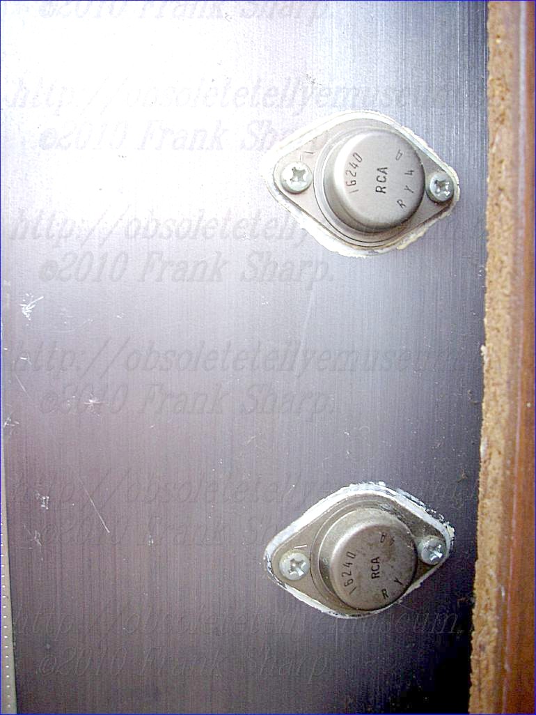
INTEGRAL THYRISTOR-RECTIFIER DEVICE BT120 BT121 (They have ext diode)A semiconductor switching device comprising a silicon controlled rectifier (SCR) and a diode rectifier integrally connected in parallel with the SCR in a single semiconductor body. The device is of the NPNP or PNPN type, having gate, cathode, and anode electrodes. A portion of each intermediate N and P region makes ohmic contact to the respective anode or cathode electrode of the SCR. In addition, each intermediate region includes a highly conductive edge portion. These portions are spaced from the adjacent external regions by relatively low conductive portions, and limit the conduction of the diode rectifier to the periphery of the device. A profile of gold recombination centers further electrically isolates the central SCR portion from the peripheral diode portion.
 That class of thyristors known as controlled rectifiers are semiconductor switches having four semiconducting regions of alternate conductivity and which employ anode, cathode, and gate electrodes. These devices are usually fabricated from silicon. In its normal state, the silicon controlled rectifier (SCR) is non-conductive until an appropriate voltage or current pulse is applied to the gate electrode, at which point current flows from the anode to the cathode and delivers power to a load circuit. If the SCR is reverse biased, it is non-conductive, and cannot be turned on by a gating signal. Once conduction starts, the gate loses control and current flows from the anode to the cathode until it drops below a certain value (called the holding current), at which point the SCR turns off and the gate electrode regains control. The SCR is thus a solid state device capable of performing the circuit function of a thyratron tube in many electronic applications. In some of these applications, such as in automobile ignition systems and horizontal deflection circuits in television receivers, it is necessary to connect a separate rectifier diode in parallel with the SCR. See, for example, W. Dietz, U. S. Pat. Nos. 3,452,244 and 3,449,623. In these applications, the anode of the rectifier diode is connected to the cathode of the SCR, and the cathode of the rectifier is connected to the SCR anode. Thus, the rectifier diode will be forward biased and current will flow through it when the SCR is reverse biased; i.e., when the SCR cathode is positive with respect to its anode. For reasons of economy and ease of handling, it would be preferable if the circuit function of the SCR and the associated diode rectifier could be combined in a single device, so that instead of requiring two devices and five electrical connections, one device and three electrical connections are all that would be necessary. In fact, because of the semiconductor profile employed, many SCR's of the shorted emitter variety inherently function as a diode rectifier when reverse biased. However, the diode rectifier function of such devices is not isolated from the controlled rectifier portion, thus preventing a rapid transition from one function to the other. Therefore, it would be desirable to physically and electrically isolate the diode rectifier portion from that portion of the device which functions as an SCR.
ZOPPAS (ZANUSSI) Z26 COLOR ELECTRONIC CHASSIS BS222 BS223 Gating circuit for television SCR deflection system AND REGULATION / stabilization of horizontal deflection NETWORK CIRCUIT with Transductor reactor / Reverse thyristor energy recovery circuit.

In a television deflection system employing a first SCR for coupling a deflection winding across a source of energy during a trace interval of each deflection cycle and a second SCR for replenishing energy to the source of energy during a commutation interval of each deflection cycle, a gating circuit for triggering the first SCR. The gating circuit employs a voltage divider coupled in parallel with the second SCR which develops gating signals proportional to the voltage across the second SCR.

1. In a television deflection system in which a first switching means couples a deflection winding across a source of energy during a trace interval of each deflection cycle and a second switching means replenishes energy to said source of energy during a commutation interval of each deflection cycle, a gating circuit for said first switching means, comprising:
capacitive voltage divider means coupled in parallel with said second switching means for developing gating signals proportional to the voltage across said second switching means; and
means for coupling said voltage divider means to said first switching means to provide for conduction of said first switching means in response to said gating signals.
2. A gating circuit according to claim 1 wherein said voltage divider includes first and second capacitors coupled in series and providing said gating signals at the common terminal of said capacitors. 3. A gating circuit according to claim 2 wherein said first and second capacitors are proportional in value to provide for the desired magnitude of gating signals. 4. A gating circuit according to claim 3 wherein said means for coupling said voltage divider means to said first switching means includes an inductor. 5. A gating circuit according to claim 4 wherein said inductor and said first and second capacitors comprise a resonant circuit having a resonant frequency chosen to shape said gating signal to improve switching of said first switching means.
TBA920 line oscillator combination
 DESCRIPTION
The line oscillator combination TBA920 is a monolithic
integrated circuit intended for the horizontal deflection of the black and white
and colour TV sets
picture tube.
FEATURES:
SYNC-PULSE SEPARATION
OPTIONAL NOISE INVERSION
GENERATION OF A LINE FREQUENCY VOL-
TAGE BY MEANS OF AN OSCILLATOR
PHASE COMPARISON BETWEEN SYNC-
PULSE AND THE OSCILLATOR WAVEFORM
PHASE COMPARISON BETWEEN THE OS-
CILLATOR WAVEFORM AND THE MIDDLE OF
THE LINE FLY-BACK PULSE
AUTOMATIC SWITCHING OF THE VARIABLE
TRANSCONDUCTANCE AND THE VARIABLE
TIME CONSTANT TO ACHIEVE NOISE SUP-
PRESSION AND, BY SWITCHING OFF, POS-
SIBILITY OF TAPE-VIDEO-REGISTERED RE-
PRODUCTION
SHAPING AND AMPLIFICATION OF THE OS-
CILLATOR WAVEFORM TO OBTAIN PULSES
FOR THE CONTROL OF DRIVING STAGES IN
HORIZONTAL, DEFLECTION CIRCUITS
USING EITHER TRANSISTORS OR THYRISTORS.
(Thyristor Horizontalsteuerung)
Horizontal deflection circuit


Description:
Description:
The present invention relates to a horizontal deflection circuit for generating the deflection current in the deflection coil of a television picture tube wherein a first switch controls the horizontal sweep, and wherein a second switch in a so-called commutation circuit with a commutating inductor and a commutating capacitor opens the first switch and, in addition, controls the energy transfer from a dc voltage source to an input inductor. The first controlled switch also forms part of a second branch circuit where it is connected in series with a second current source and a reactance capable of oscillating. When the first switch is closed, the reactance, consisting essentially of a coil and a capacitor, receives energy from the second current source during a fixed time interval. This energy which is taken from the second current source corresponds to the circuit losses caused during the previous deflection cycle.
As can be seen, such a circuit needs two different, separate inductive elements, it being known that inductive elements are expensive to manufacture and always have a certain volume determined by the electrical properties required.
The object of the invention is to reduce the amount of inductive elements required.
The invention is characterized in that the input inductor and the commutating inductor are combined in a unit designed as a transformer which is proportioned so that the open-circuit inductance of the transformer is essentially equal to the value of the input inductor, while the short-circuit inductance of the transformer is essentially equal to the value of the commutating inductor, and that the second switch is connected in series with the dc voltage source and a first winding of the transformer.
This solution has an added advantage in that, in mass production, both the open-circuit and the short-circuit inductance are reproducible with reliability.
According to another feature of the invention, the electrical isolation between the windings of the transformer is such that the transformer operates as an isolation transformer between the supply and the subcircuits connected to a second winding or to additional windings of the transformer. In this manner, the transformer additionally provides reliable mains isolation.
According to a further feature of the invention, the second switch is connected between ground and that terminal of the first winding of the transformer not connected to the supply potential. This simplifies the control of the switch.
According to a further feature of the invention, to regulate the energy supply, the second winding of the transformer is connected in series with the first switch, the commutating capacitor, and a third, bipolar switch controllable as a function of the value of a controlled variable developed in the deflection circuit.
The advantage gained by this measure lies in the fact that the control takes place on the side separated from the mains, so no separate isolation device is required for the gating of the third switch. Further details and advantages will be apparent from the following description of the accompanying drawings and from the claims. In the drawings,
FIG. 1 is a basic circuit diagram of the arrangement disclosed in German Auslegeschrift (DT-AS) No. 1,537,308;
FIG. 2 shows a first embodiment of the horizontal deflection circuit according to the invention, and
FIG. 3 shows a development of the horizontal deflection circuit according to the invention.
FIG. 1 shows the essential circuit elements of the horizontal deflection circuit known from the German Auslegeschrift (DT-AS) No. 1,537,308 referred to by way of introduction.
Connected in series with a dc voltage source UB is an input inductor Le and a bipolar, controlled switch S2. In the following, this switch will be referred to as the "second switch"; it is usually called the "commutating switch" to indicate its function.
In known circuits, the second switch S2 consists of a controlled rectifier and a diode connected in inverse parallel.
The second switch S2 also forms part of a second circuit which contains, in addition, a commutating inductor Lk, a commutating capacitor Ck, and a first switch S1. The first switch S1, controlling the horizontal sweep, is constructed in the same manner as the above-described second switch S2, consisting of a controlled rectifier and a diode in inverse parallel. Connected in parallel with this first switch is a deflection-coil arrangement AS with a capacitor CA as well as a high voltage generating arrangement (not shown). In FIGS. 1, 2, and 3, this arrangement is only indicated by an arrow and by the reference characters Hsp. The operation of this known horizontal deflection circuit need not be explained here in detail since it is described not only in the German Auslegeschrift referred to by way of introduction, but also in many other publications.
FIGS. 2 and 3 show the horizontal deflection circuit modified in accordance with the present invention. Like circuit elements are designated by the same reference characters as in FIG. 1.
FIG. 2 shows the basic principle of the invention. The two inductors Le and Lk of FIG. 1 have been replaced by a transformer U. To be able to serve as a substitute for the two inductors Le and Lk, the transformer must be proportioned in a special manner. Regardless of the turns ratio, the open-circuit inductance of the transformer is chosen to be essentially equal to the value of the input inductor Le, and the short-circuit inductance of the transformer is essentially equal to the value of the commutating inductor Lk.
To permit the second switch S2 to be utilized for the connection of the dc voltage source UB, it is included in the circuit of that winding U1 of the transformer connected to the dc voltage UB.
In principle, it is of no consequence for the operation of the switch S2 whether it is inserted on that side of the winding U1 connected to the positive operating potential +UB or on the side connected to ground. In practice, however, the solution shown in FIGS. 2 and 3 will be chosen since the gating of the controlled rectifier is less problematic in this case.
In compliance with pertinent safety regulations, the transformer U may be designed as an isolation transformer and can thus provide mains separation, which is necessary for various reasons. It is known from German Offenlegungschrift (DT-OS) No. 2,233,249 to provide dc isolation by designing the commutating inductor as a transformer, but this measure is not suited to attaining the object of the present invention.
If the energy to be taken from the dc voltage source is to be controlled as a function of the energy needed in the horizontal deflection circuit and in following subcircuits, the embodiment of the horizontal deflection circuit of FIG. 3 may be used.
The circuit including the winding U2 of the transformer U contains a third controlled switch S3, which, too, is inserted on the grounded side of the winding U2 for the reasons mentioned above. This third switch S3, just as the second switch S2, is operated at the frequency of a horizontal oscillator HO, but a control circuit RS whose input l is fed with a controlled variable is inserted between the oscillator and the switch S3. Depending on this controlled variable, the controlled rectifier of the third switch S3 can be caused to turn on earlier. A suitable controlled variable containing information on the energy consumption is, for example, the flyback pulse capable of being taken from the high voltage generating circuit (not shown). Details of the operation of this kind of energy control are described in applicant's German Offenlegungsschrift (DT-OS) No. b 2,253,386 and do not form part of the present invention.
With mains isolation, the additional, third switch S3 shown here has the advantage of being on the side isolated from the mains and eliminates the need for an isolation device in the control lead of the controlled rectifier.
As an isolation transformer, the transformer U may also carry additional windings U3 and U4 if power is to be supplied to the audio output stage, for example; in addition, the first switch S1 may be gated via such an additional winding.
The points marked at the windings U1 and U2 indicate the phase relationship between the respective voltages. Connected in parallel with the winding U1 and the second switch S2 is a capacitor CE which completes the circuit for the horizontal-frequency alternating current; this serves in particular to bypass the dc voltage source or the electrolytic capacitors contained therein.
If required, a well-known tuning coil may be inserted, e.g. in series with the second winding U2, without changing the basic operation of the horizontal deflection circuit according to the invention.
Electron beam deflection circuit including thyristors Further Discussion and deepening of knowledge, Thyristor horizontal output circuits:ZOPPAS (ZANUSSI) Z26 COLOR ELECTRONIC CHASSIS BS222 BS223

2. A deflection circuit as claimed in claim 1, wherein said amount of additional current is greater than or equal to 5 per cent of the peak-to-peak value of the current flowing through the deflection winding.
3. A deflection circuit as claimed in claim 1, wherein said means for drawing a substantial amount of additional current through said first switching means comprises a resistor connected in parallel to said first capacitor.
4. A deflection circuit as claimed in claim 1, wherein said means for drawing an additional current is formed by connecting said first and second energy sources in series so that the current charging said reactive circuit means forms the said additional current.
5. A deflection circuit as claimed in claim 1, further including a series combination of an autotransformer winding and a second high-value capacitor, said combination being connected in parallel to said first switching means, wherein said autotransformer comprises an intermediate tap located between its terminals respectively connected to said first switching means and to said second capacitor, said tap delivering, during said trace portion, a suitable DC supply voltage lower than the voltage across said second capacitor; and wherein said means for drawing a substantial amount of additional current comprises a load to be fed by said supply voltage and having one terminal connected to ground; and further controllable switching means controlled to conduct during at least part of said trace portion and to remain cut off during said retrace portion, said further switching means being connected between said tap and the other terminal of said load.
Description:
The present invention relates to electron beam deflection circuits including thyristors, such as silicon controlled rectifiers and relates, in particular, to horizontal deflection circuits for television receivers.
 The present invention constitutes an improvement in the circuit described in U.S. Pat. No. 3,449,623 filed on Sept. 6, 1966, this circuit being described in greater detail below with reference to FIGS. 1 and 2 of the accompanying drawings. A deflection circuit of this type comprises a first thyristor switch which allows the conenction of the horizontal deflection winding to a constant voltage source during the time interval used for the transmisstion of the picture signal and for applying this signal to the grid of the cathode ray tube (this interval will be termed the "trace portion" of the scan), and a second thyristor switch which provides the forced commutation of the first one by applying to it a reverse current of equal amplitude to that which passes through it from the said voltage source and thus to initiate the retrace during the horizontal blanking interval.
A undirectional reverse blocking triode type thyristor or silicon controlled rectifier (SCR), such as that used in the aformentioned circuit, requires a certain turn-off time between the instant at which the anode current ceases and the instant at which a positive bias may be applied to it without turning it on, due to the fact that there is still a high concentration of free carriers in the vicinity of the middle junction, this concentration being reduced by a process of recombination independently from the reverse polarity applied to the thyristor. This turn-off time of the thyristor is a function of a number of parameters such as the junction temperature, the DC current level, the decay time of the direct current, the peak level of the reverse current applied, the amplitude of the reverse anode to cathode voltage, the external impedance of the gate electrode, and so on, certain of these varying considerably from one thyristor to another.
In horizontal deflection circuits for television receivers, the flyback or retrace time is limited to approximately 20 percent of the horizontal scan period, the retrace time being in the case of the CCIR standard of 625 lines, approximately 12 microseconds and, in the case of the French standard of 819 lines, approximately 9 microseconds. During this relatively short interval, the thyristor has to be rendered non-conducting and the electron beam has to be returned to the origin of the scan. The first thyristor is blocked by means of a series resonant LC circuit which is subject to a certain number of restrictions (limitations as to the component values employed) due to the fact that, inter alia, it simultaneously determines the turn-off time of the circuit which blocks the thyristor and it forms part of the series resonant circuit which is to carry out the retrace. To obtain proper operation of the deflection circuit of the aforementioned Patent, especially when used for the French standard of 819 lines per image, the values of the components used have to subject to very close tolerances (approximately 2%), which results in high costs.
The improved deflection circuit, object of the present invention, allows the lengthening of the turn-off time of the circuit for turning the scan thyristor off, without altering the values of the LC circuit, which are determined by other criteria, and without impairing the operation of the circuit.
 According to the invention, there is provided an electron beam deflection circuit for a cathode ray tube with electromagentic deflection by means of a sawtooth current waveform having a trace portion and a retrace portion, said circuit comprising: a deflection winding; a first source of electrical energy formed by a first capacitor; first controllable switching means comprising a parallel combination of a first thyristor and a first diode, connected together to conduct in opposite directions, for connecting said winding to said first source during said trace portion when said first switching means is turned on; a second source of electrical energy including a first inductive energy storage means coupled to a voltage supply; reactive circuit means including a combination of inductive and capacitive reactances for storing the energy supplied by the said second source; a second controllable switching means, substantially identical with the first one, for completing a circuit including said reactive circuit means and said first switching means, when turned on, so as to pass through said first thyristor an oscillatory current in the opposite direction to that which passes through it from said first source and to turn it off after these two currents cancel out, the oscillatory current then flowing through said first diode for an interval termed the circuit turn-off time which has to be greater than the turn-off time of said first thyristor; and means for drawing duing at least a part of said trace portion a substantial amount of additional current from said first switching means in the direction of conduction of said first diode, whereby said circuit turn-off time is lengthened in proportion to the amount of said additional current, without altering the values of the reactances in the reactive circuit by shifting the waveform of the current flowing through said first switching means towards the negative by an amount equal to that of said additional current.
A further object of the invention consists in using the supplementary current in the recovery diode of the first switching means to produce a DC voltage which may be used as a power supply for the vertical deflection circuit of the television receiver, for example.
The invention will be better understood and other features and advantages thereof will become apparent from the following description and the accompanying drawings, given by way of example, and in which:
FIG. 1 is a schematic circuit diagram partially in bloc diagram form of a prior art deflection circuit according to the aforementioned Patent;
FIG. 2 shows waveforms of currents and voltages generated at various points in the circuit of FIG. 1;
FIG. 3 is a schematic diagram of a deflection circuit according to the invention which allows the principle of the improvement to be explained;
FIG. 4 is a diagram of the waveforms of the current through the first switching means 4, 5 of the circuit of FIG. 3;
FIG. 5 is a circuit diagram of another embodiment of the circuit according to the invention;
FIG. 6 is a schematic representation of the preferred embodiment of the circuit according to the invention; and
FIG. 7 shows voltage waveforms at various points of the high voltage autotransformer 21 of FIG. 6.
In all these Figures the same reference numerals refer to the same components.
FIG. 1 shows the horizontal deflection circuit described and claimed in the U.S. Pat. No. 3,449,623 mentioned above, which comprises a first source of electrical energy in the shape of a first capacitor 2 having a high capacitance C 2 for supplying a substantially constant voltage Uc 2 across its terminals. A first terminal of the first capacitor 2 is connected to ground, whilst its second terminal which supplies a positive voltage is connected to one of the terminals of a horizontal deflection winding shown as a first inductance 1. A first switching means 3, consisting of a first reverse blocking triode thyristor 4 (SCR) and a first recovery diode 5 in parallel, the two being interconnected to conduct current in opposite directions, is connected in parallel with the series combination formed by the deflection winding 1 and the first capacitor 2. The assembly of components 1, 2, 4 and 5 forms the final stage of the horizontal deflection circuit in a television receiver using electromagnetic delfection.
The deflection circuit also includes a drive stage for this final stage which here controls the turning off of the first thyristor 4 to produce the retrace or fly-back portion of the scan during the line-blanking intervals i.e. while the picture signal is not transmitted. This driver stage comprises a second voltage source in the shape of a DC power supply 6 which delivers a constant high voltage E. The negative terminal of the power supply 6 is connected to ground and its positive terminal to one of the terminals of a second inductance 7 of relatively high value, which draws a substantially lineraly varying current from the power supply 6 to avoid its overloading. The other terminal of the second inductance 7 is connected, on the one hand, to the junction of the deflection winding 1 and the first switching means 3 by means of a second inductance 8 and a second capacitor 9 in series and, on the other hand, to one of the terminals of a second controllable bi-directionally conducting switching means 10, similar to the first one 3, including a parallel combination of a second thyristor 11 and a second recovery diode 12 also arranged to conduct in opposite directions.

The respective values of the third inductance 8 (L 8 ) and of the second capacitor 9 (C 9 ) are principally selected so that, on the one hand, one half-cycle of oscillation of the first series resonant circuit L 8 - C 9 , (i.e. π √ L 8 . C 9 ) is longer than the turn-off time of the first thyristor 4, but still is as short as possible since this time interval determines the speed of the commutation of the thyristor 4, and, on the other hand, one half-cycle of oscillation of another series resonant circuit formed by L 1 , L 8 and C 9 , i.e. π √ (L 1 + L 8 ) . C 9 , is substantially equal to the required retrace time interval (i.e. shorter than the horizontal blanking interval).
The gate (control electrode) of the second thyristor 11 is coupled to the output of the horizontal oscillator 13 of the television receiver by means of a first pulse transformer 14 and a first pulse shaping circuit 15 so that it is fed short triggering pulses which are to turn it on.
The gate of the first thyristor 4 fed with signals of a substantially rectangular waveform which are negative during the horizontal blanking intervals, is coupled to a winding 16 by means of a second pulse shaping circuit 17, the winding 16 being magnetically coupled to the second inductance 7 to make up the secondary winding of a transformer of which the inductance 7 forms the primary winding. It will be noted here that it is also possible to couple the secondary winding 16 magnetically to a primary winding connected to a suitable output (not shown) of the horizontal oscillator 13.
The operation of a circuit of this type will be explained below with reference to FIG. 2 which shows the waveforms at various points in the circuit of FIG. 1 during approximately one line period.
FIG. 2 is not to scale since one line period (t 7 - t 0 ) is equal to 64 microseconds in the case of 625 lines and 49 microseconds in the case of 819 lines, while the durations of the respective horizontal blanking intervals are approximately 12 and 9.5 microseconds.
Waveform A shows the form of the current i L1 passing through deflection winding 1, this current having a sawtooth waveform substantially linear from t 0 to t 3 and from t 5 to t 7 , and crossing zero at time instants t 0 and t 7 , and reaching values of + I 1m and - I 1m , at time instants t 3 and t 5 respectively, these being its maximum positive and negative amplitudes.
During the second half of the trace portion of the horizontal deflection cycle, that is to say from t 0 to t 3 , the thyristor 4 of the first switching means 3 is conductive and makes the high value capacitor 2 discharge through the deflector winding 1, which has a high inductance, so that current i L1 increases linearly.
A few microseconds (5 to 8 μ s) before the end of the trace portion, i.e. at time instant t 1 , the trigger of the second thyristor 11 receives a short voltage pulse V G11 which causes it to turn on as its anode is at this instant at a positive potential with respect to ground, which is due to the charging of the second capacitor 9 through inductances 7 and 8 by the voltage E from the power supply 6.
When thyristor 11 is made conductive at time t 1 , on the one hand, inductance 7 is connected between ground and the voltage source 6 and a linearly increasing current flows through it and, on the other hand, the reactive circuit 8, 9 forms a loop through the second and first switching means 10 and 3, thus forming a resonant circuit which draws an oscillatory current i 8 ,9 of frequency ##EQU1##
This oscillatory current i 8 ,9 will pass through the first switching means 3, i.e. thyristor 4 and diode 5, in the opposite direction to that of current i L1 . Since the frequency f 1 is high, current i 8 ,9 will increase more rapidly than i L1 and will reach the same level at time t 2 , that is to say i 8 ,9 (t 2 ) = -i L1 (t 2 ) and these currents will cancel out in the thyristor 4 in accordance with the well known principle of forced commutation. After time instant t 2 , current i 8 ,9 continues to increase more rapidly than i L1 , but the difference between them (i 8 ,9 - i L1 ) passes the diode 5 (see wave form B) until it becomes zero at time instant t 3 which is the turn off time instant of the first switching means 3, at which the retrace begins.
The
interval between the time instant t 2 and t 3 , i.e. (t 3 -t 2 ), during which diode 5 is conductive and the thyristor is reverse biased will be termed in what follows the circuit turn-off time and it should be greater than the turn-off time of the thyristor 4 itself since the latter will subsequently become foward biased (i.e. from t 3 to t 5 ) by the retrace or flyback pulse (see waveform E) which should not trigger it.
At time instant t 3 , the switching means 3 is opened (i 4 and i 5 are both zero -- see waveforms B and C) and the reactive circuit 8, 9 forms a loop through capacitor 2 and the deflection coil 1 and thus a series resonant circuit including (L 1 + L 8 ) and C 9 , C 2 being of high value and representing a short circuit for the flyback frequency ##EQU2## thus obtained.
The retrace which stated at time t 3 takes place during one half-cycle of the resonant circuit formed by reactances L 1 , L 8 and C 9 , i.e. during the interval between t 3 and t 5 . In the middle of this interval i.e. at time instant t 4 , both i L1 (waveform A) and i 8 ,9 (waveform D) pass through zero and change their sign, whereas the voltage at the terminals of the first switching means 3 (V 3 , waveform E) passes through a maximum. Thus, from t 4 onwards, thyristor 11 will be reverse biased and diode 12 will conduct the current from the resonant circuit 1, 8 and 9 in order to turn the second thyristor 11 off.
At time instant t 5 , when current i L1 has reached - I 1m and when voltage v 3 falls to zero, diode 5 of the first switching means 3 becomes conductive and the trace portion of scan begins.
Current i 8 ,9 nevertheless continues to flow in the resonant circuit 8, 9 through diodes 5 and 12, which causes a break to appear in waveform D at t 5 , and a negative peak to appear in waveform D and a positive one in waveform B in the interval between t 5 and t 6 , these being principally due to the distributed capacities of coil 1 or to an eventual capacitor (not shown) connected in parallel to the first switching means 3.
At time instant t 6 , diode 12 of the second switching means 10 ceases to conduct after having allowed thyristor 11 time to become turned off completely.
The level of current i 8 ,9 at time instant t 5 (i.e. I c ) as well as the negative peak I D12 in i 8 ,9 and the positive peak I D5 in i 5 depend on the values of L 8 and C 9 in the same way as does the turn-off time of the circuit (t 3 - t 2 ). If, for example, L 8 and C 9 , are increased I D5 increases towards zero and this could cause diode 5 to be cut off in an undesirable fashion. I c also increases towards zero, which is liable to cause diode 12 to be blocked and thyristor 11 to trigger prematurely.
From the foregoing it can be clearly seen that the choice of values for L 8 and C 9 is subject to four limitations which prevent the values from being increased to lengthen the turn-off time of the driver circuit of first switching thyristor 4 so as to forestall its spurious triggering.
Waveform F shows the voltage v G4 obtained at the gate of thyristor 4 from the secondary winding 16 coupled to the inductor 7. This voltage is positive from t 0 to t 1 and from t 6 to t 7 and is negative between t 2 and t 6 i.e. while the second switching means 10 is conducting.
The present invention makes the lengthening of the turn-off time of thyristor 4 possible without altering the parameters of the circuit such as inductance 8 and capacitor 9.
 In the circuit shown in FIG. 3, which illustrates the principle of the present invention, means are added to the circuit in FIG. 1 which enable the turn-off time to be lengthened by connecting a load to diode 5 so as to increase the current which flows through it during the time that it is conductive. These means are here formed by a resistor 18 connected in parallel with a capacitor 20 (which replaces capacitor 2) which is of a higher capacitance so that, in practice, it holds its charge during at least one half of the line period. FIG. 4, which shows the waveform of the current in the first switching means 3 for a circuit as shown in FIG. 3, makes it possible to explain how this lenthening of the turn-off time is achieved.
In FIG. 4, the broken lines show the waveform of the current in the first switch device 3 in the circuit of FIG. 1, this waveform being produced by adding waveforms B and C of FIG. 2. The current i 4 above the axis flows through thyristor 4 and current i 5 below the axis flows through diode 5. When the capacitance C 20 of the capacitor in series with the deflector coil is increased to some tens of microfarads (C 2 having been of the order of 1 μ F) and when there is connected in parallel with capacitor 20 a resistor 18 the value of which is calculated to draw a strong current I R18 from capacitor 20, that is to say a current at least equal to 0,1 I m (I m being of the order of some tens of amperes), current I R18 is added to that i 5 which flows through diode 5 without in any way altering the linearity of the trace portion nor the oscillatory commutation of thyristor 4 which is brought about by the resonant circuit L 8 , C 9 .
The fact of loading capacitor C 20 by means of a resistor 18 thus has the effect of permanently displacing the waveform of the current in the negative direction by I R18 . Thus, during the trace portion of the scan, the transfer of the current from the diode 5 to the thyristor 4 begins at time t 10 instead of t 0 , that is to say with a delay proportional to I R18 . The effect of the triggering pulse delivered by the horizontal oscillator (13 FIG. 1) to the second thyristor 11 at time instant t 1 , will be to start the commutation process of the first thyristor 4 when the current it draws is less by I R18 than that i 4 (t 1 ) which it would have been drawing had there been no resistor 18. Because of this, the turn-off time of the thyristor 4 proper, which as has been mentioned increases with the maximum current level passing throught it, is slightly reduced. Moreover, because the oscillatory current i 8 ,9 (FIG. 2) from circuit L 8 , C 9 which flows through thyristor 4 in the opposite direction is unchanged, it reaches a value equal to that of the current i L1 (FIG. 1) flowing in the coil 1 in a shorter time, that is to say at time t 12 . Diode 5 will thus take the oscillatory current i 8 ,9 (FIG. 2) over in advance with respect ro time instant t 2 and will conduct it until it reaches zero value at a time instant t 13 later than t 3 , the amounts of advance (t 2 - t 12 ) and delay (t 13 - t 3 ) being practically equal.
It can thus be seen in FIG. 4 that the circuit turn-off time T R of a circuit according to the invention and illustrated by FIG. 3 is distinctly longer than that T r of the circuit in FIG. 1. This increase in the turn-off time (T R - T r ) depends on the current I R18 and increases therewith.
It should be noted at this point that the current I R18 produces a voltage drop at the terminals of the resistor the only effect of which is to heat up the resistor since the level of this voltage (40 to 60 volts) does not necessarily have a suitable value to be used as a voltage supply for other circuits in an existing transistorised television receiver.
In accordance with one embodiment of the invention, illustrated in FIG. 5, an application is proposed for the additional current which is to be drawn through diode 5. In FIG. 5, the positive terminal of capacitor 20 is connected by a conductor 19 to the negative pole of the power supply 6 and the voltage at the terminals of capacitor 20 is thus added to that E from the source 6.
In the preferred embodiment of the present invention, which is shown in FIG. 6, it is possible to cause a supplementary current of a desired value to flow through the first diode 5 while obtaining a voltage which has a suitable value for use in another circuit in the television receiver.
If the voltage at the terminals of capacitor 20 in FIG. 3 is not a usable value, it is possible to connect in parallel with the series circuit comprising the deflector coil 1 and the capacitor 2 in FIG. 1, i.e. in parallel with the terminals of the first switching means 3, a series combination of an autotransformer 21 and a high value capacitor 22 (comparable with capacitor 20 in FIGS. 3 and 5). The autotransformer 21 has a tap 23 is suitably positioned between the terminal connected to capacitor 22 at the tap 24 connected to the first switching means 3. This autotransformer 21 may be formed by the one conventionally used for supplying a very high voltage to the cathode ray tube, as described for example in U.S. Pat. No. 3,452,244; such a transformer comprises a voltage step-up winding between taps 24 and 25, which latter is connected to a high voltage rectifier (not shown).
The waveform of the voltage at the various points in the autotransformer is shown in FIG. 7, in which waveform A shows the voltage at the terminals of capacitor 22, waveform B the voltage at tap 24 and waveform C the voltage at tap 23 of the autotransformer 21.
The voltage V c22 at the terminals of capacitor 22 varies slightly about a mean value V cm . It is increasing while diode 5 is conducting and decreasing during the conduction of the thyristor 4.
The voltage v 24 at tap 24 follows substantially the same curve as waveform E in FIG. 2, that is to say that during the retrace time interval from t 13 to t 5 to a positive pulse called the flyback pulse is produced and, during the time interval while the first switching means 3 is conducting, the voltage is zero. The mean valve of the voltage v 24 at tap 24 of the auto-transformer 21 is equal to the mean value V cm of the voltage at the terminals of capacitors 2 and 22.
Thus, there is obtained at tap 23 a waveform which is made up, during the retrace portion, of a positive pulse whose maximum amplitude is less than that of v 24 at tap 24 and, during the trace portion, of a substantially constant positive voltage, the level V of which is less than the mean value V cm of the voltage v c22 at the terminals of capacitor 22. By moving tap 23 towards terminals 24 the amplitude of the pulse during fly-back increases while voltage V falls and conversely by moving tap 23 towards capacitor 22 voltage V increases and the amplitude of the pulse drops.
In more exact terms, the voltage V at tap 23 is such that the means value of v 23 is equal to V cm . It has thus been shown that by choosing carefully the position of tape 23, a voltage V may be obtained during the trace portion of the scan, which may be of any value between V cm and zero.
This voltage V is thus obtained by periodically controlled rectification during the trace portion of the scan. For this purpose an electronic switch is used to periodically connect the tap 23 of trnasformer winding 21 to a load. This switch is made up of a power transistor 26 whose collector is connected to tap 23 and the emitter to a parallel combination formed by a high value filtering capacitor 27 and the load which it is desired to supply, which is represented by a resistor 28. The base of the transistor 26 receives a control voltage to block it during retrace and to unblock it during the whole or part of the trace period. A control voltage of this type may be obtained from a second winding 29 magnetically coupled to the inductance 7 of the deflection circuit and it may be transmitted to the base of transistor 26 by means of a coupling capacitor 30 and a resistor 31 connected between the base and the emitter of transistor 26.
It may easily be seen that the DC collector/emitter current in transistor 26 flows through the first diode 5 of the first switching means 3 via a resistor 28 and the part of the winding of auto-transformer 21 located between taps 23 and 24.
Experience has shown that a circuit as shown in FIG. 6 can supply 24 volts with a current of 2 amperes to the vertical deflection circuit of the same television set, the voltage at the terminals of capacitor 22 being from 50 to 60 volts.
 It should be mentioned that, when the circuit which forms the load of the controlled rectifier 26, 27 does not draw enough current to sufficiently lengthen the circuit turn-off time T R , an additional resistor (not shown) may be connected between the emitter of transistor 26 and ground or in parallel to capacitor 22, which resistor will draw the additional current required.
 The present invention constitutes an improvement in the circuit described in U.S. Pat. No. 3,449,623 filed on Sept. 6, 1966, this circuit being described in greater detail below with reference to FIGS. 1 and 2 of the accompanying drawings. A deflection circuit of this type comprises a first thyristor switch which allows the conenction of the horizontal deflection winding to a constant voltage source during the time interval used for the transmisstion of the picture signal and for applying this signal to the grid of the cathode ray tube (this interval will be termed the "trace portion" of the scan), and a second thyristor switch which provides the forced commutation of the first one by applying to it a reverse current of equal amplitude to that which passes through it from the said voltage source and thus to initiate the retrace during the horizontal blanking interval.
A undirectional reverse blocking triode type thyristor or silicon controlled rectifier (SCR), such as that used in the aformentioned circuit, requires a certain turn-off time between the instant at which the anode current ceases and the instant at which a positive bias may be applied to it without turning it on, due to the fact that there is still a high concentration of free carriers in the vicinity of the middle junction, this concentration being reduced by a process of recombination independently from the reverse polarity applied to the thyristor. This turn-off time of the thyristor is a function of a number of parameters such as the junction temperature, the DC current level, the decay time of the direct current, the peak level of the reverse current applied, the amplitude of the reverse anode to cathode voltage, the external impedance of the gate electrode, and so on, certain of these varying considerably from one thyristor to another.
In horizontal deflection circuits for television receivers, the flyback or retrace time is limited to approximately 20 percent of the horizontal scan period, the retrace time being in the case of the CCIR standard of 625 lines, approximately 12 microseconds and, in the case of the French standard of 819 lines, approximately 9 microseconds. During this relatively short interval, the thyristor has to be rendered non-conducting and the electron beam has to be returned to the origin of the scan. The first thyristor is blocked by means of a series resonant LC circuit which is subject to a certain number of restrictions (limitations as to the component values employed) due to the fact that, inter alia, it simultaneously determines the turn-off time of the circuit which blocks the thyristor and it forms part of the series resonant circuit which is to carry out the retrace. To obtain proper operation of the deflection circuit of the aforementioned Patent, especially when used for the French standard of 819 lines per image, the values of the components used have to subject to very close tolerances (approximately 2%), which results in high costs.
The improved deflection circuit, object of the present invention, allows the lengthening of the turn-off time of the circuit for turning the scan thyristor off, without altering the values of the LC circuit, which are determined by other criteria, and without impairing the operation of the circuit.
A further object of the invention consists in using the supplementary current in the recovery diode of the first switching means to produce a DC voltage which may be used as a power supply for the vertical deflection circuit of the television receiver, for example.
The invention will be better understood and other features and advantages thereof will become apparent from the following description and the accompanying drawings, given by way of example, and in which:
FIG. 1 is a schematic circuit diagram partially in bloc diagram form of a prior art deflection circuit according to the aforementioned Patent;
FIG. 2 shows waveforms of currents and voltages generated at various points in the circuit of FIG. 1;FIG. 3 is a schematic diagram of a deflection circuit according to the invention which allows the principle of the improvement to be explained;
FIG. 4 is a diagram of the waveforms of the current through the first switching means 4, 5 of the circuit of FIG. 3;
FIG. 5 is a circuit diagram of another embodiment of the circuit according to the invention;
FIG. 6 is a schematic representation of the preferred embodiment of the circuit according to the invention; and
FIG. 7 shows voltage waveforms at various points of the high voltage autotransformer 21 of FIG. 6.
In all these Figures the same reference numerals refer to the same components.
FIG. 1 shows the horizontal deflection circuit described and claimed in the U.S. Pat. No. 3,449,623 mentioned above, which comprises a first source of electrical energy in the shape of a first capacitor 2 having a high capacitance C 2 for supplying a substantially constant voltage Uc 2 across its terminals. A first terminal of the first capacitor 2 is connected to ground, whilst its second terminal which supplies a positive voltage is connected to one of the terminals of a horizontal deflection winding shown as a first inductance 1. A first switching means 3, consisting of a first reverse blocking triode thyristor 4 (SCR) and a first recovery diode 5 in parallel, the two being interconnected to conduct current in opposite directions, is connected in parallel with the series combination formed by the deflection winding 1 and the first capacitor 2. The assembly of components 1, 2, 4 and 5 forms the final stage of the horizontal deflection circuit in a television receiver using electromagnetic delfection.The deflection circuit also includes a drive stage for this final stage which here controls the turning off of the first thyristor 4 to produce the retrace or fly-back portion of the scan during the line-blanking intervals i.e. while the picture signal is not transmitted. This driver stage comprises a second voltage source in the shape of a DC power supply 6 which delivers a constant high voltage E. The negative terminal of the power supply 6 is connected to ground and its positive terminal to one of the terminals of a second inductance 7 of relatively high value, which draws a substantially lineraly varying current from the power supply 6 to avoid its overloading. The other terminal of the second inductance 7 is connected, on the one hand, to the junction of the deflection winding 1 and the first switching means 3 by means of a second inductance 8 and a second capacitor 9 in series and, on the other hand, to one of the terminals of a second controllable bi-directionally conducting switching means 10, similar to the first one 3, including a parallel combination of a second thyristor 11 and a second recovery diode 12 also arranged to conduct in opposite directions.
The respective values of the third inductance 8 (L 8 ) and of the second capacitor 9 (C 9 ) are principally selected so that, on the one hand, one half-cycle of oscillation of the first series resonant circuit L 8 - C 9 , (i.e. π √ L 8 . C 9 ) is longer than the turn-off time of the first thyristor 4, but still is as short as possible since this time interval determines the speed of the commutation of the thyristor 4, and, on the other hand, one half-cycle of oscillation of another series resonant circuit formed by L 1 , L 8 and C 9 , i.e. π √ (L 1 + L 8 ) . C 9 , is substantially equal to the required retrace time interval (i.e. shorter than the horizontal blanking interval).
The gate (control electrode) of the second thyristor 11 is coupled to the output of the horizontal oscillator 13 of the television receiver by means of a first pulse transformer 14 and a first pulse shaping circuit 15 so that it is fed short triggering pulses which are to turn it on.
The gate of the first thyristor 4 fed with signals of a substantially rectangular waveform which are negative during the horizontal blanking intervals, is coupled to a winding 16 by means of a second pulse shaping circuit 17, the winding 16 being magnetically coupled to the second inductance 7 to make up the secondary winding of a transformer of which the inductance 7 forms the primary winding. It will be noted here that it is also possible to couple the secondary winding 16 magnetically to a primary winding connected to a suitable output (not shown) of the horizontal oscillator 13.
The operation of a circuit of this type will be explained below with reference to FIG. 2 which shows the waveforms at various points in the circuit of FIG. 1 during approximately one line period.
FIG. 2 is not to scale since one line period (t 7 - t 0 ) is equal to 64 microseconds in the case of 625 lines and 49 microseconds in the case of 819 lines, while the durations of the respective horizontal blanking intervals are approximately 12 and 9.5 microseconds.Waveform A shows the form of the current i L1 passing through deflection winding 1, this current having a sawtooth waveform substantially linear from t 0 to t 3 and from t 5 to t 7 , and crossing zero at time instants t 0 and t 7 , and reaching values of + I 1m and - I 1m , at time instants t 3 and t 5 respectively, these being its maximum positive and negative amplitudes.
During the second half of the trace portion of the horizontal deflection cycle, that is to say from t 0 to t 3 , the thyristor 4 of the first switching means 3 is conductive and makes the high value capacitor 2 discharge through the deflector winding 1, which has a high inductance, so that current i L1 increases linearly.
A few microseconds (5 to 8 μ s) before the end of the trace portion, i.e. at time instant t 1 , the trigger of the second thyristor 11 receives a short voltage pulse V G11 which causes it to turn on as its anode is at this instant at a positive potential with respect to ground, which is due to the charging of the second capacitor 9 through inductances 7 and 8 by the voltage E from the power supply 6.
When thyristor 11 is made conductive at time t 1 , on the one hand, inductance 7 is connected between ground and the voltage source 6 and a linearly increasing current flows through it and, on the other hand, the reactive circuit 8, 9 forms a loop through the second and first switching means 10 and 3, thus forming a resonant circuit which draws an oscillatory current i 8 ,9 of frequency ##EQU1##
This oscillatory current i 8 ,9 will pass through the first switching means 3, i.e. thyristor 4 and diode 5, in the opposite direction to that of current i L1 . Since the frequency f 1 is high, current i 8 ,9 will increase more rapidly than i L1 and will reach the same level at time t 2 , that is to say i 8 ,9 (t 2 ) = -i L1 (t 2 ) and these currents will cancel out in the thyristor 4 in accordance with the well known principle of forced commutation. After time instant t 2 , current i 8 ,9 continues to increase more rapidly than i L1 , but the difference between them (i 8 ,9 - i L1 ) passes the diode 5 (see wave form B) until it becomes zero at time instant t 3 which is the turn off time instant of the first switching means 3, at which the retrace begins.
The
At time instant t 3 , the switching means 3 is opened (i 4 and i 5 are both zero -- see waveforms B and C) and the reactive circuit 8, 9 forms a loop through capacitor 2 and the deflection coil 1 and thus a series resonant circuit including (L 1 + L 8 ) and C 9 , C 2 being of high value and representing a short circuit for the flyback frequency ##EQU2## thus obtained.
The retrace which stated at time t 3 takes place during one half-cycle of the resonant circuit formed by reactances L 1 , L 8 and C 9 , i.e. during the interval between t 3 and t 5 . In the middle of this interval i.e. at time instant t 4 , both i L1 (waveform A) and i 8 ,9 (waveform D) pass through zero and change their sign, whereas the voltage at the terminals of the first switching means 3 (V 3 , waveform E) passes through a maximum. Thus, from t 4 onwards, thyristor 11 will be reverse biased and diode 12 will conduct the current from the resonant circuit 1, 8 and 9 in order to turn the second thyristor 11 off.
At time instant t 5 , when current i L1 has reached - I 1m and when voltage v 3 falls to zero, diode 5 of the first switching means 3 becomes conductive and the trace portion of scan begins.
Current i 8 ,9 nevertheless continues to flow in the resonant circuit 8, 9 through diodes 5 and 12, which causes a break to appear in waveform D at t 5 , and a negative peak to appear in waveform D and a positive one in waveform B in the interval between t 5 and t 6 , these being principally due to the distributed capacities of coil 1 or to an eventual capacitor (not shown) connected in parallel to the first switching means 3.
At time instant t 6 , diode 12 of the second switching means 10 ceases to conduct after having allowed thyristor 11 time to become turned off completely.
The level of current i 8 ,9 at time instant t 5 (i.e. I c ) as well as the negative peak I D12 in i 8 ,9 and the positive peak I D5 in i 5 depend on the values of L 8 and C 9 in the same way as does the turn-off time of the circuit (t 3 - t 2 ). If, for example, L 8 and C 9 , are increased I D5 increases towards zero and this could cause diode 5 to be cut off in an undesirable fashion. I c also increases towards zero, which is liable to cause diode 12 to be blocked and thyristor 11 to trigger prematurely.
From the foregoing it can be clearly seen that the choice of values for L 8 and C 9 is subject to four limitations which prevent the values from being increased to lengthen the turn-off time of the driver circuit of first switching thyristor 4 so as to forestall its spurious triggering.
Waveform F shows the voltage v G4 obtained at the gate of thyristor 4 from the secondary winding 16 coupled to the inductor 7. This voltage is positive from t 0 to t 1 and from t 6 to t 7 and is negative between t 2 and t 6 i.e. while the second switching means 10 is conducting.
The present invention makes the lengthening of the turn-off time of thyristor 4 possible without altering the parameters of the circuit such as inductance 8 and capacitor 9.
 In the circuit shown in FIG. 3, which illustrates the principle of the present invention, means are added to the circuit in FIG. 1 which enable the turn-off time to be lengthened by connecting a load to diode 5 so as to increase the current which flows through it during the time that it is conductive. These means are here formed by a resistor 18 connected in parallel with a capacitor 20 (which replaces capacitor 2) which is of a higher capacitance so that, in practice, it holds its charge during at least one half of the line period. FIG. 4, which shows the waveform of the current in the first switching means 3 for a circuit as shown in FIG. 3, makes it possible to explain how this lenthening of the turn-off time is achieved.
In FIG. 4, the broken lines show the waveform of the current in the first switch device 3 in the circuit of FIG. 1, this waveform being produced by adding waveforms B and C of FIG. 2. The current i 4 above the axis flows through thyristor 4 and current i 5 below the axis flows through diode 5. When the capacitance C 20 of the capacitor in series with the deflector coil is increased to some tens of microfarads (C 2 having been of the order of 1 μ F) and when there is connected in parallel with capacitor 20 a resistor 18 the value of which is calculated to draw a strong current I R18 from capacitor 20, that is to say a current at least equal to 0,1 I m (I m being of the order of some tens of amperes), current I R18 is added to that i 5 which flows through diode 5 without in any way altering the linearity of the trace portion nor the oscillatory commutation of thyristor 4 which is brought about by the resonant circuit L 8 , C 9 .
The fact of loading capacitor C 20 by means of a resistor 18 thus has the effect of permanently displacing the waveform of the current in the negative direction by I R18 . Thus, during the trace portion of the scan, the transfer of the current from the diode 5 to the thyristor 4 begins at time t 10 instead of t 0 , that is to say with a delay proportional to I R18 . The effect of the triggering pulse delivered by the horizontal oscillator (13 FIG. 1) to the second thyristor 11 at time instant t 1 , will be to start the commutation process of the first thyristor 4 when the current it draws is less by I R18 than that i 4 (t 1 ) which it would have been drawing had there been no resistor 18. Because of this, the turn-off time of the thyristor 4 proper, which as has been mentioned increases with the maximum current level passing throught it, is slightly reduced. Moreover, because the oscillatory current i 8 ,9 (FIG. 2) from circuit L 8 , C 9 which flows through thyristor 4 in the opposite direction is unchanged, it reaches a value equal to that of the current i L1 (FIG. 1) flowing in the coil 1 in a shorter time, that is to say at time t 12 . Diode 5 will thus take the oscillatory current i 8 ,9 (FIG. 2) over in advance with respect ro time instant t 2 and will conduct it until it reaches zero value at a time instant t 13 later than t 3 , the amounts of advance (t 2 - t 12 ) and delay (t 13 - t 3 ) being practically equal.
It can thus be seen in FIG. 4 that the circuit turn-off time T R of a circuit according to the invention and illustrated by FIG. 3 is distinctly longer than that T r of the circuit in FIG. 1. This increase in the turn-off time (T R - T r ) depends on the current I R18 and increases therewith.It should be noted at this point that the current I R18 produces a voltage drop at the terminals of the resistor the only effect of which is to heat up the resistor since the level of this voltage (40 to 60 volts) does not necessarily have a suitable value to be used as a voltage supply for other circuits in an existing transistorised television receiver.
In accordance with one embodiment of the invention, illustrated in FIG. 5, an application is proposed for the additional current which is to be drawn through diode 5. In FIG. 5, the positive terminal of capacitor 20 is connected by a conductor 19 to the negative pole of the power supply 6 and the voltage at the terminals of capacitor 20 is thus added to that E from the source 6.
In the preferred embodiment of the present invention, which is shown in FIG. 6, it is possible to cause a supplementary current of a desired value to flow through the first diode 5 while obtaining a voltage which has a suitable value for use in another circuit in the television receiver.
If the voltage at the terminals of capacitor 20 in FIG. 3 is not a usable value, it is possible to connect in parallel with the series circuit comprising the deflector coil 1 and the capacitor 2 in FIG. 1, i.e. in parallel with the terminals of the first switching means 3, a series combination of an autotransformer 21 and a high value capacitor 22 (comparable with capacitor 20 in FIGS. 3 and 5). The autotransformer 21 has a tap 23 is suitably positioned between the terminal connected to capacitor 22 at the tap 24 connected to the first switching means 3. This autotransformer 21 may be formed by the one conventionally used for supplying a very high voltage to the cathode ray tube, as described for example in U.S. Pat. No. 3,452,244; such a transformer comprises a voltage step-up winding between taps 24 and 25, which latter is connected to a high voltage rectifier (not shown).
The waveform of the voltage at the various points in the autotransformer is shown in FIG. 7, in which waveform A shows the voltage at the terminals of capacitor 22, waveform B the voltage at tap 24 and waveform C the voltage at tap 23 of the autotransformer 21.
The voltage V c22 at the terminals of capacitor 22 varies slightly about a mean value V cm . It is increasing while diode 5 is conducting and decreasing during the conduction of the thyristor 4.
The voltage v 24 at tap 24 follows substantially the same curve as waveform E in FIG. 2, that is to say that during the retrace time interval from t 13 to t 5 to a positive pulse called the flyback pulse is produced and, during the time interval while the first switching means 3 is conducting, the voltage is zero. The mean valve of the voltage v 24 at tap 24 of the auto-transformer 21 is equal to the mean value V cm of the voltage at the terminals of capacitors 2 and 22.
Thus, there is obtained at tap 23 a waveform which is made up, during the retrace portion, of a positive pulse whose maximum amplitude is less than that of v 24 at tap 24 and, during the trace portion, of a substantially constant positive voltage, the level V of which is less than the mean value V cm of the voltage v c22 at the terminals of capacitor 22. By moving tap 23 towards terminals 24 the amplitude of the pulse during fly-back increases while voltage V falls and conversely by moving tap 23 towards capacitor 22 voltage V increases and the amplitude of the pulse drops.
In more exact terms, the voltage V at tap 23 is such that the means value of v 23 is equal to V cm . It has thus been shown that by choosing carefully the position of tape 23, a voltage V may be obtained during the trace portion of the scan, which may be of any value between V cm and zero.
This voltage V is thus obtained by periodically controlled rectification during the trace portion of the scan. For this purpose an electronic switch is used to periodically connect the tap 23 of trnasformer winding 21 to a load. This switch is made up of a power transistor 26 whose collector is connected to tap 23 and the emitter to a parallel combination formed by a high value filtering capacitor 27 and the load which it is desired to supply, which is represented by a resistor 28. The base of the transistor 26 receives a control voltage to block it during retrace and to unblock it during the whole or part of the trace period. A control voltage of this type may be obtained from a second winding 29 magnetically coupled to the inductance 7 of the deflection circuit and it may be transmitted to the base of transistor 26 by means of a coupling capacitor 30 and a resistor 31 connected between the base and the emitter of transistor 26.
It may easily be seen that the DC collector/emitter current in transistor 26 flows through the first diode 5 of the first switching means 3 via a resistor 28 and the part of the winding of auto-transformer 21 located between taps 23 and 24.
Experience has shown that a circuit as shown in FIG. 6 can supply 24 volts with a current of 2 amperes to the vertical deflection circuit of the same television set, the voltage at the terminals of capacitor 22 being from 50 to 60 volts.
That class of thyristors known as controlled rectifiers are semiconductor switches having four semiconducting regions of alternate conductivity and which employ anode, cathode, and gate electrodes. These devices are usually fabricated from silicon. In its normal state, the silicon controlled rectifier (SCR) is non-conductive until an appropriate voltage or current pulse is applied to the gate electrode, at which point current flows from the anode to the cathode and delivers power to a load circuit. If the SCR is reverse biased, it is non-conductive, and cannot be turned on by a gating signal. Once conduction starts, the gate loses control and current flows from the anode to the cathode until it drops below a certain value (called the holding current), at which point the SCR turns off and the gate electrode regains control. The SCR is thus a solid state device capable of performing the circuit function of a thyratron tube in many electronic applications. In some of these applications, such as in automobile ignition systems and horizontal deflection circuits in television receivers, it is necessary to connect a separate rectifier diode in parallel with the SCR. See, for example, W. Dietz, U. S. Pat. Nos. 3,452,244 and 3,449,623. In these applications, the anode of the rectifier diode is connected to the cathode of the SCR, and the cathode of the rectifier is connected to the SCR anode. Thus, the rectifier diode will be forward biased and current will flow through it when the SCR is reverse biased; i.e., when the SCR cathode is positive with respect to its anode. For reasons of economy and ease of handling, it would be preferable if the circuit function of the SCR and the associated diode rectifier could be combined in a single device, so that instead of requiring two devices and five electrical connections, one device and three electrical connections are all that would be necessary. In fact, because of the semiconductor profile employed, many SCR's of the shorted emitter variety inherently function as a diode rectifier when reverse biased. However, the diode rectifier function of such devices is not isolated from the controlled rectifier portion, thus preventing a rapid transition from one function to the other. Therefore, it would be desirable to physically and electrically isolate the diode rectifier portion from that portion of the device which functions as an SCR.ZOPPAS (ZANUSSI) Z26 COLOR ELECTRONIC CHASSIS BS222 BS223 Gating circuit for television SCR deflection system AND REGULATION / stabilization of horizontal deflection NETWORK CIRCUIT with Transductor reactor / Reverse thyristor energy recovery circuit.
In a television deflection system employing a first SCR for coupling a deflection winding across a source of energy during a trace interval of each deflection cycle and a second SCR for replenishing energy to the source of energy during a commutation interval of each deflection cycle, a gating circuit for triggering the first SCR. The gating circuit employs a voltage divider coupled in parallel with the second SCR which develops gating signals proportional to the voltage across the second SCR.

1. In a television deflection system in which a first switching means couples a deflection winding across a source of energy during a trace interval of each deflection cycle and a second switching means replenishes energy to said source of energy during a commutation interval of each deflection cycle, a gating circuit for said first switching means, comprising:
capacitive voltage divider means coupled in parallel with said second switching means for developing gating signals proportional to the voltage across said second switching means; and
means for coupling said voltage divider means to said first switching means to provide for conduction of said first switching means in response to said gating signals.
2. A gating circuit according to claim 1 wherein said voltage divider includes first and second capacitors coupled in series and providing said gating signals at the common terminal of said capacitors. 3. A gating circuit according to claim 2 wherein said first and second capacitors are proportional in value to provide for the desired magnitude of gating signals. 4. A gating circuit according to claim 3 wherein said means for coupling said voltage divider means to said first switching means includes an inductor. 5. A gating circuit according to claim 4 wherein said inductor and said first and second capacitors comprise a resonant circuit having a resonant frequency chosen to shape said gating signal to improve switching of said first switching means.
Description:
BACKGROUND OF THE INVENTION
This invention relates to a gating circuit for controlling a switching device employed in a deflection circuit of a television receiver.


Various deflection system designs have been utilized in television receivers. One design employing two bidirectional conducting switches and utilizing SCR's (thyristors) as part of the switches is disclosed in U.S. Pat. No. 3,452,244. In this type deflection system, a first SCR is


 employed for coupling a deflection winding across a source of energy during a trace interval of each deflection cycle, and a second SCR is employed for replenishing energy during a commutation interval of each deflection cycle. The first SCR is commonly provided with gating voltage by means of a separate winding or tap of an input reactor coupling a source of B+ to the second SCR.
Various regulator system designs have been utilized in conjunction with the afore described deflection system to provide for uniform high voltage production as well as uniform picture width with varying line voltage and kinescope beam current conditions.
One type regulator system design alters the amount of energy stored in a commutating capacitor coupled between the first and second SCR's during the commutating interval. A regulator design of this type may employ a regulating SCR and diode for coupling the input reactor to the source of B+. With this type regulator a notch, the width of which depends upon the regulation requirements, is created in the current supplied through the reactor and which notch shows up in the voltage waveform developed on the separate winding or tap of the input reactor which provides the gating voltage for the first SCR. The presence of the notch, even though de-emphasized by a waveshaping circuit coupling the gating voltage to the first SCR, causes erratic control of the first SCR.
SUMMARY OF THE INVENTION
In accordance with one embodiment of the invention, a gating circuit of a television deflection system employing a first switching means for coupling a deflection winding across a source of energy during a trace interval of each deflection cycle and a second switching means for replenishing energy to said source of energy during a commutation interval of each deflection cycle includes a voltage divider means coupled in parallel with the second switching means for developing gating signals proportional to the voltage across the second switching means. The voltage divider means are coupled to the first switching means to provide for conduction of the first switching means in response to the gating signals.
A more detailed description of a preferred embodiment of the invention is given in the following description and accompanying drawing of which:
FIG. 1 is a schematic diagram, partially in block form, of a prior art SCR deflection system;
FIG. 2 is a schematic diagram, partially in block form, of an SCR deflection system of the type shown in FIG. 1 including a gating circuit embodying the invention;
FIG. 3 is a schematic diagram, partially in block form, of one type of a regulator system which employs an SCR as a control device and which is suitable for use with the SCR deflection system of FIG.2;
FIG. 4 is a schematic diagram, partially in block form, of another type of a regulator system suitable for use with the deflection circuit of FIG. 2; and
FIG. 5 is a schematic diagram, partially in block form, of still another type of a regulator system suitable for use with the SCR deflection system of FIG. 2.
DESCRIPTION OF THE PREFERRED EMBODIMENT
FIG. 1 is a schematic diagram, partially in block form, of a prior art deflection system of the retrace driven type similar to that disclosed in U.S. Pat. No. 3,452,244. This system includes a commutating switch 12, comprising a silicon controlled rectifier (SCR) 14 and an oppositely poled damper diode 16. The commutating switch 12 is coupled between a winding 18a of an input choke 18 and ground. The other terminal of winding 18a is coupled to a source of direct current voltage (B+) by means of a regulator network 20 which controls the energy stored in the deflection circuit 10 when the commutating switch is off, during an interval T3 to T0' as shown in curve 21 which is a plot of the voltage level at the anode of SCR 14 during the deflection cycle. A damping network comprising a series combination of a resistor 22 and a capacitor 23 is coupled in parallel with commutating switch 12 and serves to reduce any ringing effects produced by the switching of commutating switch 12. Commutating switch 12 is coupled through a commutating coil 24, a commutating capacitor 25 and a trace switch 26 to ground. Trace switch 26 comprises an SCR 28 and an oppositely poled damper diode 30. An auxiliary capacitor 32 is coupled between the junction of coil 24 and capacitor 25 and ground. A series combination of a horizontal deflection winding 34 and an S-shaping capacitor 36 are coupled in parallel with trace switch 26. Also, a series combination of a primary winding 38a of a horizontal output transformer 38 and a DC blocking capacitor 40 are coupled in parallel with trace switch 26.
A secondary of high voltage winding 38b of transformer 38 produces relatively large amplitude flyback pulses during the retrace interval of each deflection cycle. This interval exists between T1 and T2 of curve 41 which is a plot of the current through windings 34 and 38a during the deflection cycle. These flyback pulses are applied to a high voltage multiplier (not shown) or other suitable means for producing direct current high voltage for use as the ultor voltage of a kinescope (not shown).
An auxiliary winding 38c of transformer 38 is coupled to a high voltage sensing and control circuit 42 which transforms the level of flyback pulses into a pulse width modulated signal. The control circuit 42 is coupled to the regulator network 20.
A horizontal oscillator 44 is coupled to the gate electrode of commutating SCR 14 and produces a pulse during each deflection cycle slightly before the end of the trace interval at T0 of curve 21 to turn on SCR 14 to initiate the commutating interval. The commutating interval occurs between T0 and T3 of curve 21. A resonant waveshaping network 46 comprising a series combination of a capacitor 48 and an inductor 50 coupled between a winding 18b of input choke 18 and the gate electrode of trace SCR 28 and a damping resistor 52 coupled between the junction of capacitor 48 and inductor 50 and ground shapes the signal developed at winding 18b (i.e. voltage waveform 53) to form a gating signal voltage waveform 55 to enable SCR 28 for conduction during the second half of the trace interval occurring between T2 and T1' of curve 41.
 The regulator network 20, when of a type to be described in conjunction with FIG. 3, operates in such a manner that current through winding 18a of input choke 18 during an interval between T4 and T5 (region A) of curves 21, 53 and 55 is interrupted for a period of time the duration of which is determined by the signal produced by the high voltage sensing and control circuit 42. During the interruption of current through winding 18a a zero voltage level is developed by winding 18b as shown in interval T4 to T5 of curve 53. The resonant waveshaping circuit 46 produces the shaped waveform 55 which undesirably retains a slump in region A corresponding to the notch A of waveform 53. The slump in waveform 55 applied to SCR 28 occurs in a region where the anode of SCR 28 becomes positive and where SCR 28 must be switched on to maintain a uniform production of the current waveshape in the horizontal deflection winding 34 as shown in curve 41. The less positive amplitude current occurring at region A of waveform 55 may result in insufficient gating current for SCR 28 and may cause erratic performance resulting in an unsatisfactory raster.
FIG. 2 is a schematic diagram, partially in block form, of a deflection system 60 embodying the invention. Those elements which perform the same function in FIG. 2 as in FIG. 1 are labeled with the same reference numerals. FIG. 2 differs from FIG. 1 essentially in that the signal to enable SCR 28 derived from sampling a portion of the voltage across commutating switch 12 rather than a voltage developed by winding 18b which is a function of the voltage across winding 18a of input choke 18 as in FIG. 1. This change eliminates the slump in the enabling signal during the interval T4 to T5 as shown in curve 64 since the voltage across the commutating switch 12 is not adversely effected by the regulator network 20 operation.
A series combination of resistor 22, capacitor 23 and a capacitor 62 is coupled in parallel with commutating switch 12, one terminal of capacitor 62 being coupled to ground. The junction of capacitors 23 and 62 is coupled to the gate electrode of SCR 28 by means of the inductor 50. The resistor 52 is coupled in parallel with capacitor 62.
Capacitors 23 and 62 form a capacitance voltage divider which provides a suitable portion of the voltage across commutating switch 12 for gating SCR 28 via inductor 50. The magnitude of the voltage at the junction of capacitors 23 and 62 is typically 25 to 35 volts. It can, therefore, be seen that the ratio of values of capacitors 23 and 62 will vary depending on the B+ voltage utilized to energize the deflection system. Capacitors 23 and 62 and inductor 50 form a resonant circuit tuned in a manner which provides for peaking of the curve 64 between T4 and T5. This peaking effect further enhances gating of SCR 28 between T4 and T5.
Since the waveshape of the voltage across commutating switch 12 (curve 21) is relatively independent of the type of regulator system employed in conjunction with the deflection system, the curve 64 also is independent of the type of regulator system.
When commutating switch 12 switches off during the interval T3 to T0' curve 21, the voltage across capacitor 62 increases and the voltage at the gate electrode of SCR 28 increases as shown in curve 64. As will be noted, no slump of curve 64 occurs between T3 and T5 because there is no interruption of the voltage across commutating switch 12.


FIG. 3 is a schematic diagram, partially in block form, of one type of a regulator system which may be used in conjunction with the invention. B+ is supplied through a regulator network 20 which comprises an SCR 66 and an oppositely poled diode 68. The diode is poled to provide for conduction of current from B+ to the horizontal deflection circuit 60 via winding 18a of input choke 18. Current flows through the diode during the period T3 to T4 of curve 21 FIG. 1 after which current tries to flow through the SCR 66 from the horizontal deflection circuit to B+ since the commutating capacitor 25 is charged to a voltage higher than B+.
The horizontal deflection circuit 60 produces a flyback pulse in winding 38a of the flyback transformer 38 which is coupled to winding 38c. The magnitude of the pulse on winding 38c determines how long the signal required to switch SCR 66 on is delayed after T4 curve 21 FIG. 1. If the flyback pulse is greater than desirable, the SCR 66 turns on sooner than if the flyback pulse is less than desirable and provides a discharge path for current in commutating capacitor 25 back to the B+ supply. In this manner a relatively constant amplitude flyback pulse is maintained.
FIG. 4 is a schematic diagram, partially in block form, of another well-known type of a regulator system which may be used in conjunction with the invention shown in FIG. 2. B+ is coupled through winding 18a of input choke 18 and through a series combination of windings 70a and 70b of a saturable reactor 70 and a parallel combination of a diode 72 and a resistor 74 to the horizontal deflection circuit 60. Diode 72 is poled to conduct current from the horizontal deflection circuit 60 to B+.
Flyback pulse variations are obtained from winding 38c of the horizontal output transformer 38 and applied to a voltage divider comprising resistors 76, 78 and 80 of the high voltage sensing and control circuit 42. A portion of the pulse produced by winding 38c is selected by the position of the wiper terminal on potentiometer 78 and coupled to the base electrode of a transistor 82 by means of a zener diode 84. The emitter electrode of transistor 82 is grounded and a DC stabilization resistor 85 is coupled in parallel with the base-emitter junction of transistor 82. When the pulse magnitude on winding 38c exceeds a level which results in forward biasing the base-emitter junction of transistor 82, current flows from B+ through a resistor 86, a winding 70c of saturable reactor 70 and transistor 82 to ground. Due to the exponential increase of current in winding 70c during the period of conduction of transistor 82, the duration of conduction of transistor 82 determines the magnitude of current flowing in winding 70c and thus the total inductance of windings 70a and 70b. The current in winding 70c is sustained during the remaining deflection period by means of a diode 88 coupled in parallel with winding 70c and poled not to conduct current from B+ to the collector electrode of transistor 82. A capacitor 90 coupled to the cathode of diode 88 provides a bypass for B+. Windings 70a and 70b are in parallel with input reactor 18a and thereby affect the total input inductance of the deflection circuit and thereby controls the transfer of energy to the deflection circuit. The dotted waveforms shown in conjunction with a curve 21' indicate variations from a nominal waveform provided at the input of horizontal deflection circuit 60 by the windings 70a and 70b.


FIG. 5 is a schematic diagram of yet another type of a regulator system which may be used in conjunction with the invention. B+ is coupled through a winding 92a and a winding 92b of a saturable reactor to the horizontal deflection circuit 60. Windings 92a and 92b are used to replace the input choke 18 shown in FIGS. 1 and 2 while also providing for a regulating function corresponding to that provided by regulating network 20.
Flyback pulse variations are obtained from winding 38c and applied to the high voltage sensing and control circuit 42 as in FIG. 4. Current flows from B+ through resistor 86, a winding 92c and transistor 82 to ground. As in FIG. 4 the duration of the conduction of transistor 82 determines the energy stored in winding 92c and thus the total inductance of windings 92a and 92b which control the amount of energy transferred to the deflection circuit during each horizontal deflection cycle. The variations in waveforms of curve 21', shown in conjunction with FIG. 4, are also provided at the input of horizontal deflection circuit 60 by windings 92a and 92b.
For various reasons including cost or performance, a manufacturer may wish to utilize a particular one of the regulators illustrated in FIGS. 3, 4 and 5. Regardless of the choice, the gating circuit according to the invention may be utilized therewith advantageously by providing improved performance and the possibility of cost savings by eliminating taps or extra windings on the wound components which heretofore normally provided a source of SCR gating waveforms.
1. A voltage multiplier having two rows of serially connected capacitors and terminals between capacitors on each row, a diode connecting each capacitor terminal on one row with a capacitor terminal on another row, all of said diodes being connected in series to pass pulses of one polarity only, said diodes being arranged to charge each capacitor, said two rows of serially connected capacitors consisting of end contacted layer capacitors which are integrally joined to one another, said end contacted layer capacitors being split into individual capacitors by slots which extend from one end face of the capacitor through the capacitive zone thereof to a point short of the opposite end face, the individual capacitors having unslotted portions of the metal coatings which serially connect each other, all of the terminals of a row of serially connected capacitors being formed in an end face, whereby said diodes may be readily connected from the terminals on the end face of one row of capacitors to the terminals on the end face of the other row of capacitors. 2. A voltage multiplier in accordance with claim 1 wherein said two rows of capacitors are arranged in side by side relation and spaced from one another, the majority of said diodes being arranged substantially parallel to one another. 3. A voltage multiplier in accordance with claim 1 wherein the terminals of each of the individual capacitors of each capacitor row lie substantially in the same plane. 4. A voltage multiplier in accordance with claim 1 wherein the two rows of capacitors are congruent in physical design, arranged on top of each other as a single integral unit separated by an intermediate insulating layer, the diodes arranged on a single side of the integral capacitor unit and extend perpendicularly to the end contact layers and are welded to the narrow edges of said end contact layer. 5. A voltage multiplier in accordance with claim 4 wherein said end contact layers are formed by the Schoop process. 6. A voltage multiplier in accordance with claim 1 wherein the two capacitor rows are arranged in spaced side by side relation, the end contact surfaces being arranged at the top of each row and lying generally in a single plane, the contact surfaces being arranged in a direction generally perpendicular to the longitudinal direction of the foils forming the capacitors, the majority of said diodes being arranged substantially parallel to one another and having their connection wires welded to the contact surfaces of said capacitor rows. 7. A voltage multiplier in accordance with claim 1 wherein one of said capacitor rows is formed on top of the other, said rows being separated by an insulating intermediate layer which does not project beyond the end contact layers, both rows of capacitors being subject in common to the Schoop process, the diodes spanning the end contact layers and being welded to the narrow edges thereof, the diodes extending in a direction generally parallel to the direction of the foils forming the capacitors. 8. A voltage multiplier in accordance with claim 1 wherein said diodes are silicon diodes. 9. A voltage multiplier comprising first and second end contacted layer capacitors, said capacitors being stacked upon each other, a plurality of substantially parallel slits extending alternately from opposite end faces of the stacked capacitor assembly to points intermediate of but not through the assembly, thereby electrically dividing the capacitor assembly into a number of individual capacitors which are serially connected by the remaining unslit portion of the metal coatings and which form the conductive layers thereof, an intermediate insulating layer separating the first and second end contacted capacitors, and a plurality of diodes arranged substantially parallel to each other and generally in a single plane which defines one side of the capacitor assembly, the diodes extending between the end contacts of the capacitor assembly and making electrical contact with the narrow edges of those end contacts. 10. A voltage multiplier in accordance with claim 9 wherein said first and second capacitors, being stacked to form an assembly, have opposite end faces contacted in common by the Schoop process, and the diodes are caused to span the capacitor assembly to make electrical contact between said opposite end faces. 11. A voltage multiplier in accordance with claim 1 wherein the two rows of serially connected capacitors are stacked one above the other and are separated by an intermediate insulating layer, said capacitors being end contacted by the schoop process, the intermediate insulating layer extending outwardly of the schoop layer, only one row of capacitors on each side thereof having free edge zones, diodes being arranged substantially parallel to said slots and making electrical contact with opposite end contact surfaces of said rows of capacitors. 12. A voltage multiplier in accordance with claim 11 wherein the portion of the intermediate insulating layer which extends outwardly of the schoop layer is free of schoop metal.
ZOPPAS (ZANUSSI) Z26 COLOR ELECTRONIC CHASSIS BS222 BS223 ELECTRICAL COMPONENT PROTECTED AGAINST HIGH TENSION, PARTICULARLY FOR COLOR TELEVISION RECEIVERS AND METHOD OF ITS PRODUCTION:Voltage multipliers of the type involved normally used in color television receivers to produce the high voltage for the picture tube anode:
A grid-shaped electrical component is formed by molding a plurality of electrically interconnected capacitors and diodes, physically forming a grid structure, within a synthetic casting resin. The electrical components form the cores of the struts of the grid structure and each strut is provided with a plurality of indentations in the synthetic resin in the area of the walls of the components.
1. A grid-shaped electrical component protected against high tension comprising a plurality of molded struts extending in substantially two grid directions and in at least one grid direction oblique thereto, each of said struts formed of synthetic resin and having a large wall strength, a plurality of electrically interconnected electrical components individually cast within and forming the respective cores or said struts, the components extending in one of said grid directions disposed to lie in one plane, the components extending in the other grid direction disposed to lie in another plane pa rallel to said one plane, the components extending in the oblique direction disposed to lie in one of said planes, said components comprising a plurality of capacitors disposed in the struts which extend in one grid direction and a plurality of rectifiers which are disposed in said struts which extend in the other grid direction and in the oblique grid direction, said capacitors forming serially connected rows of capacitors and said rectifiers connected to the ends of said capacitors, a first group of conductors disposed at one end of said grid structure and having the individual conductors thereof connected to the junctions of said electrical components and each including a portion extending substantially parallel to the respective capacitors and a portion extending through said grid structure generally perpendicular to the first-mentioned portions, and a second group of electrical conductors at the other end of said grid structure connected to the junctions of said electrical components thereat, said grid structure further including a base having mounting shoulders formed thereon, said grid structure together with said base and said conductors forming a self-supporting structure for permitting the passage of cooling air between said struts.
This invention relates to a gating circuit for controlling a switching device employed in a deflection circuit of a television receiver. 


Various deflection system designs have been utilized in television receivers. One design employing two bidirectional conducting switches and utilizing SCR's (thyristors) as part of the switches is disclosed in U.S. Pat. No. 3,452,244. In this type deflection system, a first SCR is


Various regulator system designs have been utilized in conjunction with the afore described deflection system to provide for uniform high voltage production as well as uniform picture width with varying line voltage and kinescope beam current conditions.
One type regulator system design alters the amount of energy stored in a commutating capacitor coupled between the first and second SCR's during the commutating interval. A regulator design of this type may employ a regulating SCR and diode for coupling the input reactor to the source of B+. With this type regulator a notch, the width of which depends upon the regulation requirements, is created in the current supplied through the reactor and which notch shows up in the voltage waveform developed on the separate winding or tap of the input reactor which provides the gating voltage for the first SCR. The presence of the notch, even though de-emphasized by a waveshaping circuit coupling the gating voltage to the first SCR, causes erratic control of the first SCR.
SUMMARY OF THE INVENTION
In accordance with one embodiment of the invention, a gating circuit of a television deflection system employing a first switching means for coupling a deflection winding across a source of energy during a trace interval of each deflection cycle and a second switching means for replenishing energy to said source of energy during a commutation interval of each deflection cycle includes a voltage divider means coupled in parallel with the second switching means for developing gating signals proportional to the voltage across the second switching means. The voltage divider means are coupled to the first switching means to provide for conduction of the first switching means in response to the gating signals. A more detailed description of a preferred embodiment of the invention is given in the following description and accompanying drawing of which:
FIG. 1 is a schematic diagram, partially in block form, of a prior art SCR deflection system;
FIG. 2 is a schematic diagram, partially in block form, of an SCR deflection system of the type shown in FIG. 1 including a gating circuit embodying the invention;
FIG. 3 is a schematic diagram, partially in block form, of one type of a regulator system which employs an SCR as a control device and which is suitable for use with the SCR deflection system of FIG.2;
FIG. 4 is a schematic diagram, partially in block form, of another type of a regulator system suitable for use with the deflection circuit of FIG. 2; and
FIG. 5 is a schematic diagram, partially in block form, of still another type of a regulator system suitable for use with the SCR deflection system of FIG. 2.
DESCRIPTION OF THE PREFERRED EMBODIMENT
FIG. 1 is a schematic diagram, partially in block form, of a prior art deflection system of the retrace driven type similar to that disclosed in U.S. Pat. No. 3,452,244. This system includes a commutating switch 12, comprising a silicon controlled rectifier (SCR) 14 and an oppositely poled damper diode 16. The commutating switch 12 is coupled between a winding 18a of an input choke 18 and ground. The other terminal of winding 18a is coupled to a source of direct current voltage (B+) by means of a regulator network 20 which controls the energy stored in the deflection circuit 10 when the commutating switch is off, during an interval T3 to T0' as shown in curve 21 which is a plot of the voltage level at the anode of SCR 14 during the deflection cycle. A damping network comprising a series combination of a resistor 22 and a capacitor 23 is coupled in parallel with commutating switch 12 and serves to reduce any ringing effects produced by the switching of commutating switch 12. Commutating switch 12 is coupled through a commutating coil 24, a commutating capacitor 25 and a trace switch 26 to ground. Trace switch 26 comprises an SCR 28 and an oppositely poled damper diode 30. An auxiliary capacitor 32 is coupled between the junction of coil 24 and capacitor 25 and ground. A series combination of a horizontal deflection winding 34 and an S-shaping capacitor 36 are coupled in parallel with trace switch 26. Also, a series combination of a primary winding 38a of a horizontal output transformer 38 and a DC blocking capacitor 40 are coupled in parallel with trace switch 26. A secondary of high voltage winding 38b of transformer 38 produces relatively large amplitude flyback pulses during the retrace interval of each deflection cycle. This interval exists between T1 and T2 of curve 41 which is a plot of the current through windings 34 and 38a during the deflection cycle. These flyback pulses are applied to a high voltage multiplier (not shown) or other suitable means for producing direct current high voltage for use as the ultor voltage of a kinescope (not shown). An auxiliary winding 38c of transformer 38 is coupled to a high voltage sensing and control circuit 42 which transforms the level of flyback pulses into a pulse width modulated signal. The control circuit 42 is coupled to the regulator network 20.
A horizontal oscillator 44 is coupled to the gate electrode of commutating SCR 14 and produces a pulse during each deflection cycle slightly before the end of the trace interval at T0 of curve 21 to turn on SCR 14 to initiate the commutating interval. The commutating interval occurs between T0 and T3 of curve 21. A resonant waveshaping network 46 comprising a series combination of a capacitor 48 and an inductor 50 coupled between a winding 18b of input choke 18 and the gate electrode of trace SCR 28 and a damping resistor 52 coupled between the junction of capacitor 48 and inductor 50 and ground shapes the signal developed at winding 18b (i.e. voltage waveform 53) to form a gating signal voltage waveform 55 to enable SCR 28 for conduction during the second half of the trace interval occurring between T2 and T1' of curve 41.
 The regulator network 20, when of a type to be described in conjunction with FIG. 3, operates in such a manner that current through winding 18a of input choke 18 during an interval between T4 and T5 (region A) of curves 21, 53 and 55 is interrupted for a period of time the duration of which is determined by the signal produced by the high voltage sensing and control circuit 42. During the interruption of current through winding 18a a zero voltage level is developed by winding 18b as shown in interval T4 to T5 of curve 53. The resonant waveshaping circuit 46 produces the shaped waveform 55 which undesirably retains a slump in region A corresponding to the notch A of waveform 53. The slump in waveform 55 applied to SCR 28 occurs in a region where the anode of SCR 28 becomes positive and where SCR 28 must be switched on to maintain a uniform production of the current waveshape in the horizontal deflection winding 34 as shown in curve 41. The less positive amplitude current occurring at region A of waveform 55 may result in insufficient gating current for SCR 28 and may cause erratic performance resulting in an unsatisfactory raster. FIG. 2 is a schematic diagram, partially in block form, of a deflection system 60 embodying the invention. Those elements which perform the same function in FIG. 2 as in FIG. 1 are labeled with the same reference numerals. FIG. 2 differs from FIG. 1 essentially in that the signal to enable SCR 28 derived from sampling a portion of the voltage across commutating switch 12 rather than a voltage developed by winding 18b which is a function of the voltage across winding 18a of input choke 18 as in FIG. 1. This change eliminates the slump in the enabling signal during the interval T4 to T5 as shown in curve 64 since the voltage across the commutating switch 12 is not adversely effected by the regulator network 20 operation.
 A series combination of resistor 22, capacitor 23 and a capacitor 62 is coupled in parallel with commutating switch 12, one terminal of capacitor 62 being coupled to ground. The junction of capacitors 23 and 62 is coupled to the gate electrode of SCR 28 by means of the inductor 50. The resistor 52 is coupled in parallel with capacitor 62.
Capacitors 23 and 62 form a capacitance voltage divider which provides a suitable portion of the voltage across commutating switch 12 for gating SCR 28 via inductor 50. The magnitude of the voltage at the junction of capacitors 23 and 62 is typically 25 to 35 volts. It can, therefore, be seen that the ratio of values of capacitors 23 and 62 will vary depending on the B+ voltage utilized to energize the deflection system. Capacitors 23 and 62 and inductor 50 form a resonant circuit tuned in a manner which provides for peaking of the curve 64 between T4 and T5. This peaking effect further enhances gating of SCR 28 between T4 and T5.
Since the waveshape of the voltage across commutating switch 12 (curve 21) is relatively independent of the type of regulator system employed in conjunction with the deflection system, the curve 64 also is independent of the type of regulator system.
When commutating switch 12 switches off during the interval T3 to T0' curve 21, the voltage across capacitor 62 increases and the voltage at the gate electrode of SCR 28 increases as shown in curve 64. As will be noted, no slump of curve 64 occurs between T3 and T5 because there is no interruption of the voltage across commutating switch 12.


 FIG. 3 is a schematic diagram, partially in block form, of one type of a regulator system which may be used in conjunction with the invention. B+ is supplied through a regulator network 20 which comprises an SCR 66 and an oppositely poled diode 68. The diode is poled to provide for conduction of current from B+ to the horizontal deflection circuit 60 via winding 18a of input choke 18. Current flows through the diode during the period T3 to T4 of curve 21 FIG. 1 after which current tries to flow through the SCR 66 from the horizontal deflection circuit to B+ since the commutating capacitor 25 is charged to a voltage higher than B+.
 The horizontal deflection circuit 60 produces a flyback pulse in winding 38a of the flyback transformer 38 which is coupled to winding 38c. The magnitude of the pulse on winding 38c determines how long the signal required to switch SCR 66 on is delayed after T4 curve 21 FIG. 1. If the flyback pulse is greater than desirable, the SCR 66 turns on sooner than if the flyback pulse is less than desirable and provides a discharge path for current in commutating capacitor 25 back to the B+ supply. In this manner a relatively constant amplitude flyback pulse is maintained.
FIG. 4 is a schematic diagram, partially in block form, of another well-known type of a regulator system which may be used in conjunction with the invention shown in FIG. 2. B+ is coupled through winding 18a of input choke 18 and through a series combination of windings 70a and 70b of a saturable reactor 70 and a parallel combination of a diode 72 and a resistor 74 to the horizontal deflection circuit 60. Diode 72 is poled to conduct current from the horizontal deflection circuit 60 to B+. Flyback pulse variations are obtained from winding 38c of the horizontal output transformer 38 and applied to a voltage divider comprising resistors 76, 78 and 80 of the high voltage sensing and control circuit 42. A portion of the pulse produced by winding 38c is selected by the position of the wiper terminal on potentiometer 78 and coupled to the base electrode of a transistor 82 by means of a zener diode 84. The emitter electrode of transistor 82 is grounded and a DC stabilization resistor 85 is coupled in parallel with the base-emitter junction of transistor 82. When the pulse magnitude on winding 38c exceeds a level which results in forward biasing the base-emitter junction of transistor 82, current flows from B+ through a resistor 86, a winding 70c of saturable reactor 70 and transistor 82 to ground. Due to the exponential increase of current in winding 70c during the period of conduction of transistor 82, the duration of conduction of transistor 82 determines the magnitude of current flowing in winding 70c and thus the total inductance of windings 70a and 70b. The current in winding 70c is sustained during the remaining deflection period by means of a diode 88 coupled in parallel with winding 70c and poled not to conduct current from B+ to the collector electrode of transistor 82. A capacitor 90 coupled to the cathode of diode 88 provides a bypass for B+. Windings 70a and 70b are in parallel with input reactor 18a and thereby affect the total input inductance of the deflection circuit and thereby controls the transfer of energy to the deflection circuit. The dotted waveforms shown in conjunction with a curve 21' indicate variations from a nominal waveform provided at the input of horizontal deflection circuit 60 by the windings 70a and 70b.


FIG. 5 is a schematic diagram of yet another type of a regulator system which may be used in conjunction with the invention. B+ is coupled through a winding 92a and a winding 92b of a saturable reactor to the horizontal deflection circuit 60. Windings 92a and 92b are used to replace the input choke 18 shown in FIGS. 1 and 2 while also providing for a regulating function corresponding to that provided by regulating network 20.
Flyback pulse variations are obtained from winding 38c and applied to the high voltage sensing and control circuit 42 as in FIG. 4. Current flows from B+ through resistor 86, a winding 92c and transistor 82 to ground. As in FIG. 4 the duration of the conduction of transistor 82 determines the energy stored in winding 92c and thus the total inductance of windings 92a and 92b which control the amount of energy transferred to the deflection circuit during each horizontal deflection cycle. The variations in waveforms of curve 21', shown in conjunction with FIG. 4, are also provided at the input of horizontal deflection circuit 60 by windings 92a and 92b.
ZOPPAS (ZANUSSI) Z26 COLOR ELECTRONIC CHASSIS BS222 BS223 Voltage multiplier:
A voltage multiplier formed by a pair of end contacted layer capacitors. The layer capacitors may be arranged side by side or may be stacked one upon the other. In each case a series of slits are cut in the capacitor to divide the unit into a plurality of individual capacitors, each being integrally connected by an unslit web. The diodes which are part of the voltage multiplier are then arranged in substantially parallel relation to extend across the capacitor body to make electrical contact between the end faces thereof.
Description:
BACKGROUND OF THE INVENTION
1. Description of the Prior Art
Voltage multipliers of the type involved in the present invention are normally used in color television receivers to produce the high voltage for the picture tube anode. The known electrical voltage multipliers of this type are normally manually assembled from individual components and are soldered together. Such an arrangement is time consuming and it is not always possible to automate the soldering process in such a method of construction.
2. Field of the Invention
The field of art to which this invention pertains is solid state voltage multipliers and in particular to such voltage multipliers which are formed of an integral arrangement of layer type capacitors end contacted by the Schoop process.
SUMMARY OF THE INVENTION
It is an important feature of the present invention to provide an improved structure for a voltage multiplier.
It is another feature of the present invention to provide a voltage multiplier using a layer type capacitor arrangement.
It is a principle object of the present invention to provide an improved solid state voltage multiplier which is subject to easy production techniques.
It is another object of the present invention to provide a voltage multiplier formed of a layer type capacitor which is manufactured in such a way as to permit a series of diodes used in the multiplier to be readily easily soldered to the capacitor terminals in a single plane.
It is an additional object of the present invention to provide a voltage multiplier as described above wherein the capacitors of the multiplier consist of two layer type capacitors, each being slit in such a way as to form two sets of series connected individual capacitors.
It is also an object of this invention to provide a voltage multiplier as described above wherein the two sets of individual capacitors are arranged in side by side spaced relation.
It is a further object of the present invention to provide a voltage multiplier as described above wherein the two sets of serially connected individual capacitors are stacked one upon the other, and the diodes used in the multiplier are caused to span the body of the capacitor assembly and make electrical contact between the end faces thereof.
These and other features, advantages and objects of the present invention will be understood in greater detail from the following description and the associated drawings wherein reference numerals are utilized as to designate the preferred embodiments.
BRIEF DESCRIPTION OF THE DRAWINGS
FIG. 1 shows a circuit diagram of a voltage multiplier in accordance with the present invention.
FIG. 2 shows a voltage multiplier in accordance with the present invention wherein two separate capacitor networks are used and arranged in side by side spaced relation.
FIG. 3 shows an arrangement having electrical characteristics similar to FIGS. 1 and 2 but wherein the capacitor networks or sets are stacked upon one another in a spaced saving arrangement.
FIG. 4 is a diagrammatic cross sectional view of the arrangement shown in FIG. 3.
FIG. 5 shows two capacitor networks which are separated by an insulating layer which extends beyond the Schoop layers.
DESCRIPTION OF THE PREFERRED EMBODIMENTS
The present invention relates to an electric voltage multiplier of the type used in television receivers to produce the high anode voltage for the picture tube. Such multipliers usually consist of two rows of serially connected capacitors with a plu rality of diodes connecting the capacitor terminals on one row with the like terminals on the other row. The diodes are connected in series to pass a unidirectional pulse and are arranged in such a way as to charge each of the capacitors.
By virtue of the present invention, there is provided a smaller physical design for a voltage multiplier and a physical construction which is easily suited to automation processes.
This is accomplished in the present invention by providing the two rows of serially connected capacitors to be formed from end contacted layer capacitors which are integrally joined together. The metal coatings of each layer of the capacitors have free edges at opposite sides, and the capacitor layers are split by a series of slits which form individual capacitors connected electrically in series. The slits pass from one end face to a point just beyond the capacitor zone of the capacitor. In each case the individual capacitors are connected in series with the other capacitors by an inner coating which is not severed in making the slits.
Capacitor networks of the type described are known from the German text laid open to public inspection No. 1,764,861. It is not possible however to achieve a simple production technique for voltage multipliers by the use of the teachings of this patent. Only by means of the combination of features of the present invention such as using an inner series connection has it been possible to develop an arrangement where all contact surfaces lie on the same end face of the capacitor network. In this way it has been possible to achieve a physical construction which enables the taking advantage of the most automated production techniques. Furthermore the use of capacitor networks which are based upon the principle of layer capacitors provides the added advantage that it is possible to use silicon diodes which are considerably smaller than the selenium rectifiers heretofore used.
In one arrangement of the invention, the two capacitor networks are arranged next to one another and the diodes are arranged substantially parallel to one another except for one of the diodes at the end of the circuit. This enhances the possibility of using automating processes. For the same reason, it is advisable for the contact surfaces to lie in a single plane which is possible according to the present invention.
A particularly space saving embodiment of the invention is provided in which the two capacitor networks are arranged one above another in a stacked manner and are separated from one another by an insulating intermediate layer which may extend beyond the Schoop layer as shown in FIG. 5.
Also, the projecting of the insulating layer and the removal of Schoop metal from the layers can be avoided if the two capacitor networks are stacked in such a way and separated by an insulating layer which does not project beyond the Schoop layers, if in the region of one end face, all the coatings of one capacitor network has free edge zones exposed. In such an arrangement each of the coatings is displaced in relation to the adjacent coatings. In such a manner the Schoop layer only covers the coatings of one of the two capacitor networks and the coatings of the other network is safely insulated from the Schoop layer by the free edge zones. At the same time, a mechanically stable structure is formed, since the Schoop layer also secures the parts of the end faces which they do not electrically contact.
A construction which is particularly advantageous is one in which the two capacitor networks are congruent and the diodes are arranged on one side of the capacitor network and welded to the Schoop layers. In this case the diodes are arranged perpendicularly to the end contact layers.
A simple process for the production of voltage multipliers according to the present invention is such that the capacitor networks are arranged in side by side spaced relation and the contact surfaces are generally in a single plane. In this arrangement the diodes are arranged in a direction perpendicular to the longitudinal direction of the foils in the capacitor, and the diodes span the end faces of the structure. A diode arranged at the beginning or end of the unit can be positioned at an angle, while the other diodes are arranged in a generally parallel orientation.
The preferred embodiment of the invention which is particularly small designed voltage multipliers consist of stacking the two layer capacitors upon each other and separating them by an insulating layer which does not project over the ends. The slits which are then formed on the capacitor layers, divide the capacitors into individual elements, and the diodes are placed in position on the top of the arrangement in such a way that the terminals of the diodes connect the end faces of the capacitor layers.
Referring to the drawings for greater detail FIG. 1 shows a schematic of a voltage multiplier according to the present invention in which capacitors 1 form one serially connected set and capacitors 2 form a second serially connected set. The capacitor network 4 of FIG. 2 is formed from the capacitors 1 of FIG. 1. The capacitor network 5 of FIG. 2 is formed in accordance with the invention from the capacitors 2 of FIG. 1. In FIG. 1 the diodes 3 are connected from the terminals of the capacitors 1 to the terminals of capacitors 2 as shown to produce a series diode arrangement which charges each of the capacitors as is well understood in the art of voltage multipliers.
The contact surface 6 (FIG. 2) is grounded, while the contact surface 7 is connected to the pulse input. Contact surface 8 is the tap for the high volta ge output and the contact surface 9 serves to contact the diodes to two of the capacitors of one capacitor network and the contact surface 22 serves to contact the last capacitor of the capacitor network 5 to two of the diodes.
As in FIG. 2, the diodes 3 are placed on the contact surfaces 7, 8, 22, and 9 and are electrically connected thereto by spot welding. Slots 10 are provided and filled with synthetic material in the course of encasing the arrangement so that they possess the requisite dielectric strength. During operation these slots are connected at least temporarily with the full voltage of a capacitor in the case of television, for example, the voltage across one of these slots may be 8.5 K.V.
In FIG. 3, an arrangement is shown where the capacitor networks 4 and 5 are congruent and are stacked one above the other. In this case, the outer flanks 11 of the capacitor networks 5 are not used. The two end faces of the capacitor networks 4 and 5 are entirely covered with Schoop layers. The diodes 3 are arranged generally in a parallel layout with respect to the slots 10. The diodes connect the opposite contact surfaces 13 and 14 of the Schoop layers.
As illustrated in FIG. 4, the contact surfaces 13 and 14 contact only the corresponding metal coatings 15 and 17 of one of the capacitor networks 4 and 5. The coating 16 of the capacitor network 4 contacts neither of the two Schoop l ayers 13 and 14. However, these coatings extend beyond the slot depth 19, so that after the completion of the capacitor network, electrically conductive arms remain outside the slots and are integrally joined to the blind coatings. Accordingly, the blind coatings 18 of the capacitor 5 project beyond the slot depth 20. Thus, it is only possible to contact such a capacitor network on one end side.
The diodes 3 can thus only be connected by welding their two terminals to in each case one contact surface 13 and 14 in accordance with FIG. 1. This construction also must be sealed in order to achieve the required dielectric strength.
The intermediate layer 21 does not project beyond the end faces of the capacitor network 4 and 5 and is covered by the Schoop layer. It prevents sparkovers in the region of the cut edges and breakdowns through the dielectric, since, particularly in the use of a multiple inner series connection, the dielectric does not possess a dielectric strength sufficient to support the voltage of the overall capacitor.
In FIG. 5 the two capacitor networks 4 and 5 are separated from each other by an insulating intermediate layer 21 which extends beyond the Schoop layers 13 and 14. The Schoop layers 13 and 14 are interrupted by this intermediate layer and the upper and lower part of the Schoop layers 13 and 14 can always be contacted and wired separately.
1. Description of the Prior Art
Voltage multipliers of the type involved in the present invention are normally used in color television receivers to produce the high voltage for the picture tube anode. The known electrical voltage multipliers of this type are normally manually assembled from individual components and are soldered together. Such an arrangement is time consuming and it is not always possible to automate the soldering process in such a method of construction.
2. Field of the Invention
The field of art to which this invention pertains is solid state voltage multipliers and in particular to such voltage multipliers which are formed of an integral arrangement of layer type capacitors end contacted by the Schoop process.
SUMMARY OF THE INVENTION
It is an important feature of the present invention to provide an improved structure for a voltage multiplier.
It is another feature of the present invention to provide a voltage multiplier using a layer type capacitor arrangement.
It is a principle object of the present invention to provide an improved solid state voltage multiplier which is subject to easy production techniques.
It is another object of the present invention to provide a voltage multiplier formed of a layer type capacitor which is manufactured in such a way as to permit a series of diodes used in the multiplier to be readily easily soldered to the capacitor terminals in a single plane.
It is an additional object of the present invention to provide a voltage multiplier as described above wherein the capacitors of the multiplier consist of two layer type capacitors, each being slit in such a way as to form two sets of series connected individual capacitors.
It is also an object of this invention to provide a voltage multiplier as described above wherein the two sets of individual capacitors are arranged in side by side spaced relation.
It is a further object of the present invention to provide a voltage multiplier as described above wherein the two sets of serially connected individual capacitors are stacked one upon the other, and the diodes used in the multiplier are caused to span the body of the capacitor assembly and make electrical contact between the end faces thereof.
These and other features, advantages and objects of the present invention will be understood in greater detail from the following description and the associated drawings wherein reference numerals are utilized as to designate the preferred embodiments.
BRIEF DESCRIPTION OF THE DRAWINGS
FIG. 2 shows a voltage multiplier in accordance with the present invention wherein two separate capacitor networks are used and arranged in side by side spaced relation.
FIG. 3 shows an arrangement having electrical characteristics similar to FIGS. 1 and 2 but wherein the capacitor networks or sets are stacked upon one another in a spaced saving arrangement.
FIG. 4 is a diagrammatic cross sectional view of the arrangement shown in FIG. 3.
FIG. 5 shows two capacitor networks which are separated by an insulating layer which extends beyond the Schoop layers.
DESCRIPTION OF THE PREFERRED EMBODIMENTS
The present invention relates to an electric voltage multiplier of the type used in television receivers to produce the high anode voltage for the picture tube. Such multipliers usually consist of two rows of serially connected capacitors with a plu
 rality of diodes connecting the capacitor terminals on one row with the like terminals on the other row. The diodes are connected in series to pass a unidirectional pulse and are arranged in such a way as to charge each of the capacitors.
By virtue of the present invention, there is provided a smaller physical design for a voltage multiplier and a physical construction which is easily suited to automation processes.
This is accomplished in the present invention by providing the two rows of serially connected capacitors to be formed from end contacted layer capacitors which are integrally joined together. The metal coatings of each layer of the capacitors have free edges at opposite sides, and the capacitor layers are split by a series of slits which form individual capacitors connected electrically in series. The slits pass from one end face to a point just beyond the capacitor zone of the capacitor. In each case the individual capacitors are connected in series with the other capacitors by an inner coating which is not severed in making the slits.
Capacitor networks of the type described are known from the German text laid open to public inspection No. 1,764,861. It is not possible however to achieve a simple production technique for voltage multipliers by the use of the teachings of this patent. Only by means of the combination of features of the present invention such as using an inner series connection has it been possible to develop an arrangement where all contact surfaces lie on the same end face of the capacitor network. In this way it has been possible to achieve a physical construction which enables the taking advantage of the most automated production techniques. Furthermore the use of capacitor networks which are based upon the principle of layer capacitors provides the added advantage that it is possible to use silicon diodes which are considerably smaller than the selenium rectifiers heretofore used.
In one arrangement of the invention, the two capacitor networks are arranged next to one another and the diodes are arranged substantially parallel to one another except for one of the diodes at the end of the circuit. This enhances the possibility of using automating processes. For the same reason, it is advisable for the contact surfaces to lie in a single plane which is possible according to the present invention.
A particularly space saving embodiment of the invention is provided in which the two capacitor networks are arranged one above another in a stacked manner and are separated from one another by an insulating intermediate layer which may extend beyond the Schoop layer as shown in FIG. 5.
A construction which is particularly advantageous is one in which the two capacitor networks are congruent and the diodes are arranged on one side of the capacitor network and welded to the Schoop layers. In this case the diodes are arranged perpendicularly to the end contact layers.
A simple process for the production of voltage multipliers according to the present invention is such that the capacitor networks are arranged in side by side spaced relation and the contact surfaces are generally in a single plane. In this arrangement the diodes are arranged in a direction perpendicular to the longitudinal direction of the foils in the capacitor, and the diodes span the end faces of the structure. A diode arranged at the beginning or end of the unit can be positioned at an angle, while the other diodes are arranged in a generally parallel orientation.
The preferred embodiment of the invention which is particularly small designed voltage multipliers consist of stacking the two layer capacitors upon each other and separating them by an insulating layer which does not project over the ends. The slits which are then formed on the capacitor layers, divide the capacitors into individual elements, and the diodes are placed in position on the top of the arrangement in such a way that the terminals of the diodes connect the end faces of the capacitor layers.
Referring to the drawings for greater detail FIG. 1 shows a schematic of a voltage multiplier according to the present invention in which capacitors 1 form one serially connected set and capacitors 2 form a second serially connected set. The capacitor network 4 of FIG. 2 is formed from the capacitors 1 of FIG. 1. The capacitor network 5 of FIG. 2 is formed in accordance with the invention from the capacitors 2 of FIG. 1. In FIG. 1 the diodes 3 are connected from the terminals of the capacitors 1 to the terminals of capacitors 2 as shown to produce a series diode arrangement which charges each of the capacitors as is well understood in the art of voltage multipliers.
The contact surface 6 (FIG. 2) is grounded, while the contact surface 7 is connected to the pulse input. Contact surface 8 is the tap for the high volta
 ge output and the contact surface 9 serves to contact the diodes to two of the capacitors of one capacitor network and the contact surface 22 serves to contact the last capacitor of the capacitor network 5 to two of the diodes.
As in FIG. 2, the diodes 3 are placed on the contact surfaces 7, 8, 22, and 9 and are electrically connected thereto by spot welding. Slots 10 are provided and filled with synthetic material in the course of encasing the arrangement so that they possess the requisite dielectric strength. During operation these slots are connected at least temporarily with the full voltage of a capacitor in the case of television, for example, the voltage across one of these slots may be 8.5 K.V.
In FIG. 3, an arrangement is shown where the capacitor networks 4 and 5 are congruent and are stacked one above the other. In this case, the outer flanks 11 of the capacitor networks 5 are not used. The two end faces of the capacitor networks 4 and 5 are entirely covered with Schoop layers. The diodes 3 are arranged generally in a parallel layout with respect to the slots 10. The diodes connect the opposite contact surfaces 13 and 14 of the Schoop layers.
As illustrated in FIG. 4, the contact surfaces 13 and 14 contact only the corresponding metal coatings 15 and 17 of one of the capacitor networks 4 and 5. The coating 16 of the capacitor network 4 contacts neither of the two Schoop l
 ayers 13 and 14. However, these coatings extend beyond the slot depth 19, so that after the completion of the capacitor network, electrically conductive arms remain outside the slots and are integrally joined to the blind coatings. Accordingly, the blind coatings 18 of the capacitor 5 project beyond the slot depth 20. Thus, it is only possible to contact such a capacitor network on one end side.
The diodes 3 can thus only be connected by welding their two terminals to in each case one contact surface 13 and 14 in accordance with FIG. 1. This construction also must be sealed in order to achieve the required dielectric strength.
The intermediate layer 21 does not project beyond the end faces of the capacitor network 4 and 5 and is covered by the Schoop layer. It prevents sparkovers in the region of the cut edges and breakdowns through the dielectric, since, particularly in the use of a multiple inner series connection, the dielectric does not possess a dielectric strength sufficient to support the voltage of the overall capacitor.
In FIG. 5 the two capacitor networks 4 and 5 are separated from each other by an insulating intermediate layer 21 which extends beyond the Schoop layers 13 and 14. The Schoop layers 13 and 14 are interrupted by this intermediate layer and the upper and lower part of the Schoop layers 13 and 14 can always be contacted and wired separately.
ZOPPAS (ZANUSSI) Z26 COLOR ELECTRONIC CHASSIS BS222 BS223 ELECTRICAL COMPONENT PROTECTED AGAINST HIGH TENSION, PARTICULARLY FOR COLOR TELEVISION RECEIVERS AND METHOD OF ITS PRODUCTION:Voltage multipliers of the type involved normally used in color television receivers to produce the high voltage for the picture tube anode:
A grid-shaped electrical component is formed by molding a plurality of electrically interconnected capacitors and diodes, physically forming a grid structure, within a synthetic casting resin. The electrical components form the cores of the struts of the grid structure and each strut is provided with a plurality of indentations in the synthetic resin in the area of the walls of the components.
 rallel to said one plane, the components extending in the oblique direction disposed to lie in one of said planes, said components comprising a plurality of capacitors disposed in the struts which extend in one grid direction and a plurality of rectifiers which are disposed in said struts which extend in the other grid direction and in the oblique grid direction, said capacitors forming serially connected rows of capacitors and said rectifiers connected to the ends of said capacitors, a first group of conductors disposed at one end of said grid structure and having the individual conductors thereof connected to the junctions of said electrical components and each including a portion extending substantially parallel to the respective capacitors and a portion extending through said grid structure generally perpendicular to the first-mentioned portions, and a second group of electrical conductors at the other end of said grid structure connected to the junctions of said electrical components thereat, said grid structure further including a base having mounting shoulders formed thereon, said grid structure together with said base and said conductors forming a self-supporting structure for permitting the passage of cooling air between said struts.
Description:
BACKGROUND OF THE INVENTION
1. Field of the Invention
This invention relates to a grid-shaped electrical component having grid struts extending substantially in two main grid directions, and more particularly to grid-shaped components which are protected against high tension, particularly for color television receivers.
2. Description of the Prior Art
Heretofore, the prior art recognized a conventional expedient to provide a color television receiver with a line transformer to generate the high voltage required for the picture tube. This line transformer was advantageously utilized to provide high voltage pulses which were then rectified prior to being employed at the picture tube. Construction of the line transformer for protection against high voltages, as well as the associated rectifier arrangement, has proven difficult in situations wherein the transformer was required to deliver the full value of the required high voltage. This is particularly true in the case of color television receivers since a direct current voltage of approximately 25kv. is ordinarily required for proper operation of the picture tube.
In view of the foregoing it is therefore advisable to design the line transformer for a lower voltage and to generate a direct current voltage of the required magnitude by utilization of a multiplier cascaded with the line transformer. For example, it is significant that the line transformer delivers recoil pulses with an amplitude of 8.5kv., from which a DC voltage of 25kv. can be obtained in a multiplier cascade having 5 silenium rectifiers and four or five capacitors.
In electrical equipment technology, however, there is always the problem, as here in a multiplier cascade, to design components free from brush discharge and protected against high tension, so that neither adjacent components nor the operating personnel can be harmed. To this end, it is generally known in the art to combine such units which are exposed to high tension into a single component which can be built in or exchanged as a one unit component both during original manufacture of the apparatus and in case of maintenance or repair.
Arrangements of the type initially mentioned avoid a majority of the inconvenience experienced heretofore by components manufactured to meet the above conditions. Thus, for example, the corresponding components are frequently cast with plastic into one compact block. However, in addition to the problem of an effective heat dissipation there is the further difficulty that the wall strength of the grouting mass between the components is not sufficiently constant, or that the metallic connecting elements of the components or the wiring may appear on the surface and cause glow defects or flash-overs.
To avoid the latter drawbacks it is also an old expedient in the art to fixedly arrange the components of the unit on a base plate and to cast the entire unit in a beaker consisting of a material which is combined with the grouting mass. However, these solutions have the drawback that casting in a beaker is relatively expensive and that as a result of these steps the problem of cooling the component parts is rendered more difficult.
Although the component parts of the type initially mentioned have great advantages from the electrical point of view as well as with regard to the manufacturing cost, there is also an additional difficulty as a result of the size of the components thus produced. In many cases, particularly in the interior of electrical apparatus such as, for example, color television sets, the measurements of which one seeks to reduce through the use of integrated switching circuits, it is frequently undesirable or even quite impossible to accommodate the component parts.
Hence, it is an object of the invention to produce an electrical component protected against high tension which has the advantages of a component of a type mentioned initially, but which has smaller dimensions than heretofore known in employing the same individual components.
SUMMARY OF THE INVENTION
According to the invention, the component parts are disposed in a molded grid structure wherein certain component parts lie in one grid direction, other component parts lie in another grid direction, and still other components are disposed obliquely to the two main grid directions. Each of the individual components are molded in a strut of the grid structure and the components parts which are disposed in one grid direction and those disposed obliquely to the grid directions are located in one plane, while the component parts disposed in the other grid direction lie in a plane parallel to the first-mentioned plane. Through this arrangement with the component parts lying in different planes, one can substantially reduce the space required for the apparatus in question without adversely affecting the advantages of prior known constructions.
As shown in relatively long experiments, it is very important for an effective operation of the apparatus that the wall strength of the synthetic resin enveloping the component parts is substantially equally large throughout the entire apparatus. It has namely been shown that the important point is that the thickness of the layer of synthetic resin varies only relatively little throughout the apparatus, and in all respects the variation is not excessive, since otherwise there may be the danger that the sealing layer will crack upon cooling. The danger of a crack formation may also be responsible for the fact that with the component parts known heretofore and case in the form of a block with or without a beaker, only adverse results were obtained since the plastics suitable for the electrical components with respect to high tension do not lend themselves to casting into blocks.
A new type of apparatus which is protected against high tension in accordance with the principles of the present invention is particularly suitable for a high tension multiplier cascade in color television sets of the type mentioned initially which contains a plurality of rectifier elements and capacitors. A further development of the invention provides that the capacitors lie parallel one behind the other in an upper plane, that in the second plane lying therebeneath a portion of the rectifier elements is spaced at a distance from the other plane and lie perpendicular to the capacitors, and that in a diagonal line of each rectangle defined by two capacitors and two rectifiers there is arranged an additional rectifier in the second lower plane. For the electrical connection of the component part with the elements of a corresponding circuit, it is provided that electrical conductors are guided outwardly from adjacent ends of the rows of capacitors, the conductors first extending a distance within the synthetic casting resin substantially parallel to the capacitors at one end of the apparatus, and at the opposite end of the apparatus the electrical conductors extend from the rows of capacitors whose ends are connected with a rectifier element and guided outwardly therefrom through the envelope of synthetic resin.
BRIEF DESCRIPTION OF THE DRAWINGS
Other objects, features and advantages of the invention will become apparent from the following detailed description taken in conjunction with the accompanying drawings, in which:
FIG. 1 is a plan view, partially in section, illustrating apparatus constructed according to the invention; and
FIG. 2 is a sectional view taken along the line II--II of FIG. 1.
DESCRIPTION OF THE PREFERRED EMBODIMENT
FIG. 1 illustrates a high tension cascade constructed in accordance with the principles of the present invention to produce the accelerating voltage required for color television tubes amounting to approximately 25 kv. consisting of five silenium rectifiers 21, 31 and four capacitors 22, fifth capacitor not cast within the component part must be separately connected thereto. Therefore, this capacitor is not shown in the drawing. The reference numerals 25, 26 and 27 designate the electrical conductors which are guided outwardly through the synthetic resin 23. The electrical conductors 25 and 26 on the base side of the component part are first pulled a distance upwardly in the synthetic resin casing so that when they exit the component part (see FIG. 2) the conductors are already sufficiently separated from the base side which is generally connected with the base frame. The indentations 24 in the synthetic resin compound are shown somewhat exaggerated schematically, since the indentations generally end, at least partly, on the wall portions of the component parts which are protected against high tension. The indentations 24 are produced during the manufacture of the cascade in accordance with the invention, wherein the interconnected electrical components which form a loose grid are placed in a mold consisting of a material, such as polyethylene or polypropylene, which does not combine with the casting resin, for example, epoxy resin. Within this mold there are disposed spacing blocks which are preferably formed directly on the mold and which are arranged and dimensioned such that they assure a sufficient space between live metal parts of the electrical components and the inner wall of the mold when the loose grid is installed. Owing to the tolerances required for a simple insertion of the grid of component parts, not all component parts will rest against all spacing blocks provided for the centering thereof so that not all of the indentations 24 in the synthetic resin compound 23 reach as far as the high tension resistant wall of the component part accommodated within the corresponding strut. The fact is illustrated schematically in the drawing where some of the indentations do not reach quite as far as the component parts.
As apparent from FIG. 2, a plastic strip 28 is provided on the narrow side (base side) of the component part remote from the high tension conductor 27, which interconnects the parallel rows of capacitors and wherein recesses 29 are provided by means of which the component part can be screwed onto the apparatus or attached in a different manner.
The invention is not limited to the embodiment shown. For example, is it also possible to form separate feet on the component for attachment purposes. It is likewise possible to slide the capacitors 22 still further inwardly by way of the rectifiers whereby a lateral contacting of the connection conductors of the capacitors is advantageous so as to make the lateral expansion of the component part still smaller. It is however, essential that the component forms a punctured grid structure since in this way there is, first, comparatively uniform wall strengths assured and, second, the cooling of the component elements can be separately effected without forcing the heat to first penetrate a larger layer of synthetic resin.
When employed in television sets, particularly color television sets, component parts in accordance with the invention may be built into advantage in horizontal position in so-called knapsacks, where as a result of their grid-shaped construction, they not only do not impede the air circulation caused by heating of the other component parts of the set, but are at the same time effectively cooled as a result of the air currents flowing therethrough.
Changes and modifications may be made of the invention within the scope and spirit of the appended claims which define what is believed to be new and desired to have protected by Letters Patent.
1. Field of the Invention
This invention relates to a grid-shaped electrical component having grid struts extending substantially in two main grid directions, and more particularly to grid-shaped components which are protected against high tension, particularly for color television receivers.
2. Description of the Prior Art
Heretofore, the prior art recognized a conventional expedient to provide a color television receiver with a line transformer to generate the high voltage required for the picture tube. This line transformer was advantageously utilized to provide high voltage pulses which were then rectified prior to being employed at the picture tube. Construction of the line transformer for protection against high voltages, as well as the associated rectifier arrangement, has proven difficult in situations wherein the transformer was required to deliver the full value of the required high voltage. This is particularly true in the case of color television receivers since a direct current voltage of approximately 25kv. is ordinarily required for proper operation of the picture tube.
In view of the foregoing it is therefore advisable to design the line transformer for a lower voltage and to generate a direct current voltage of the required magnitude by utilization of a multiplier cascaded with the line transformer. For example, it is significant that the line transformer delivers recoil pulses with an amplitude of 8.5kv., from which a DC voltage of 25kv. can be obtained in a multiplier cascade having 5 silenium rectifiers and four or five capacitors.
In electrical equipment technology, however, there is always the problem, as here in a multiplier cascade, to design components free from brush discharge and protected against high tension, so that neither adjacent components nor the operating personnel can be harmed. To this end, it is generally known in the art to combine such units which are exposed to high tension into a single component which can be built in or exchanged as a one unit component both during original manufacture of the apparatus and in case of maintenance or repair.
Arrangements of the type initially mentioned avoid a majority of the inconvenience experienced heretofore by components manufactured to meet the above conditions. Thus, for example, the corresponding components are frequently cast with plastic into one compact block. However, in addition to the problem of an effective heat dissipation there is the further difficulty that the wall strength of the grouting mass between the components is not sufficiently constant, or that the metallic connecting elements of the components or the wiring may appear on the surface and cause glow defects or flash-overs.
To avoid the latter drawbacks it is also an old expedient in the art to fixedly arrange the components of the unit on a base plate and to cast the entire unit in a beaker consisting of a material which is combined with the grouting mass. However, these solutions have the drawback that casting in a beaker is relatively expensive and that as a result of these steps the problem of cooling the component parts is rendered more difficult.
Although the component parts of the type initially mentioned have great advantages from the electrical point of view as well as with regard to the manufacturing cost, there is also an additional difficulty as a result of the size of the components thus produced. In many cases, particularly in the interior of electrical apparatus such as, for example, color television sets, the measurements of which one seeks to reduce through the use of integrated switching circuits, it is frequently undesirable or even quite impossible to accommodate the component parts.
Hence, it is an object of the invention to produce an electrical component protected against high tension which has the advantages of a component of a type mentioned initially, but which has smaller dimensions than heretofore known in employing the same individual components.
SUMMARY OF THE INVENTION
As shown in relatively long experiments, it is very important for an effective operation of the apparatus that the wall strength of the synthetic resin enveloping the component parts is substantially equally large throughout the entire apparatus. It has namely been shown that the important point is that the thickness of the layer of synthetic resin varies only relatively little throughout the apparatus, and in all respects the variation is not excessive, since otherwise there may be the danger that the sealing layer will crack upon cooling. The danger of a crack formation may also be responsible for the fact that with the component parts known heretofore and case in the form of a block with or without a beaker, only adverse results were obtained since the plastics suitable for the electrical components with respect to high tension do not lend themselves to casting into blocks.
A new type of apparatus which is protected against high tension in accordance with the principles of the present invention is particularly suitable for a high tension multiplier cascade in color television sets of the type mentioned initially which contains a plurality of rectifier elements and capacitors. A further development of the invention provides that the capacitors lie parallel one behind the other in an upper plane, that in the second plane lying therebeneath a portion of the rectifier elements is spaced at a distance from the other plane and lie perpendicular to the capacitors, and that in a diagonal line of each rectangle defined by two capacitors and two rectifiers there is arranged an additional rectifier in the second lower plane. For the electrical connection of the component part with the elements of a corresponding circuit, it is provided that electrical conductors are guided outwardly from adjacent ends of the rows of capacitors, the conductors first extending a distance within the synthetic casting resin substantially parallel to the capacitors at one end of the appa
ratus, and at the opposite end of the apparatus the electrical conductors extend from the rows of capacitors whose ends are connected with a rectifier element and guided outwardly therefrom through the envelope of synthetic resin.BRIEF DESCRIPTION OF THE DRAWINGS
Other objects, features and advantages of the invention will become apparent from the following detailed description taken in conjunction with the accompanying drawings, in which:
FIG. 1 is a plan view, partially in section, illustrating apparatus constructed according to the invention; and
FIG. 2 is a sectional view taken along the line II--II of FIG. 1.
DESCRIPTION OF THE PREFERRED EMBODIMENT
FIG. 1 illustrates a high tension cascade constructed in accordance with the principles of the present invention to produce the accelerating voltage required for color television tubes amounting to approximately 25 kv. consisting of five silenium rectifiers 21, 31 and four capacitors 22, fifth capacitor not cast within the component part must be separately connected thereto. Therefore, this capacitor is not shown in the drawing. The reference numerals 25, 26 and 27 designate the electrical conductors which are guided outwardly through the synthetic resin 23. The electrical conductors 25 and 26 on the base side of the component part are first pulled a distance upwardly in the synthetic resin casing so that when they exit the component part (see FIG. 2) the conductors are already sufficiently separated from the base side which is generally connected with the base frame. The indentations 24 in the synthetic resin compound are shown somewhat exaggerated schematically, since the indentations generally end, at least partly, on the wall portions of the component parts which are protected against high tension. The indentations 24 are produced during the manufacture of the cascade in accordance with the invention, wherein the interconnected electrical components which form a loose grid are placed in a mold consisting of a material, such as polyethylene or polypropylene, which does not combine with the casting resin, for example, epoxy resin. Within this mold there are disposed spacing blocks which are preferably formed directly on the mold and which are arranged and dimensioned such that they assure a sufficient space between live metal parts of the electrical components and the inner wall of the mold when the loose grid is installed. Owing to the tolerances required for a simple insertion of the grid of component parts, not all component parts will rest against all spacing blocks provided for the centering thereof so that not all of the indentations 24 in the synthetic resin compound 23 reach as far as the high tension resistant wall of the component part accommodated within the corresponding strut. The fact is illustrated schematically in the drawing where some of the indentations do not reach quite as far as the component parts.
As apparent from FIG. 2, a plastic strip 28 is provided on the narrow side (base side) of the component part remote from the high tension conductor 27, which interconnects the parallel rows of capacitors and wherein recesses 29 are provided by means of which the component part can be screwed onto the apparatus or attached in a different manner.
When employed in television sets, particularly color television sets, component parts in accordance with the invention may be built into a
dvantage in horizontal position in so-called knapsacks, where as a result of their grid-shaped construction, they not only do not impede the air circulation caused by heating of the other component parts of the set, but are at the same time effectively cooled as a result of the air currents flowing therethrough.Changes and modifications may be made of the invention within the scope and spirit of the appended claims which define what is believed to be new and desired to have protected by Letters Patent.
ZOPPAS (ZANUSSI) Z26 COLOR ELECTRONIC CHASSIS BS222 BS223 Television Voltage multiplier arrangement with capacitor rolls surrounded by diodes:
A voltage multiplier includes a plurality of capacitors and diodes in an integral unit. The capacitors are combined in capacitor rolls surrounded by diodes on the outside of the diodes can be positioned between two capacitor rolls. AC and dc-voltage-operated capacitors can be combined in separate or the same rolls. The ac capacitors may be located inside within the roll and the dc capacitors on the outside of the same roll. The capacitor plates are made of aluminum foil with intermediate polystyrene and polyester layers. A common capacitor electrode plate may be used for adjacent capacitors.
1. A voltage multiplier comprising a plurality of series connected diodes and a plurality of capacitors, each capacitor being connected between opposite ends of a pair of said diodes and including an intermediate thermoplastic dielectric layer and a pair of metal foil electrode layers on opposite sides of said dielectric layer, said electrode and dielectric layers being rolled into a plurality of overlapping layers including said plurality of capacitors within a common roll, said diodes being connected to said electrode layers and being disposed about opposite outer sides of said roll. 2. The device of claim 1 including means applying a.c. and d.c. voltages to different respective groups of said capacitors. 3. The device of claim 1 wherein said plurality of diodes surround the sides and one end of said roll, the other end of said roll having external connections thereto, and a common thermoplastic cover encapsulating said diodes and capacitors, said external connections extending from one end of said cover. 4. The device of claim 1 including means applying a.c. and d.c. voltages to different respective groups of said capacitors within said common roll, said a.c. voltage capacitors being within the inner layers and said d.c. voltage capacitors being within the outer layers. 5. The device of claim 1 wherein said roll has external connections to the two ends thereof. 6. The device of claim 1 wherein said thermoplastic dielectric layer includes two outer layers of polystyrene and a layer of polyester therebetween. 7. The device of claim 1 wherein one electrode layer is common to two capacitors within said roll. 8. The device of claim 6 wherein said electrode layers are of aluminum.
1. A voltage multiplier comprising a plurality of series connected diodes and a plurality of capacitors, each capacitor being connected between opposite ends of a pair of said diodes and including an intermediate thermoplastic dielectric layer and a pair of metal foil electrode layers on opposite sides of said dielectric layer, said electrode and dielectric layers being rolled into a plurality of overlapping layers including said plurality of capacitors within a common roll, said diodes being connected to said electrode layers and being disposed about opposite outer sides of said roll. 2. The device of claim 1 including means applying a.c. and d.c. voltages to different respective groups of said capacitors. 3. The device of claim 1 wherein said plurality of diodes surround the sides and one end of said roll, the other end of said roll having external connections thereto, and a common thermoplastic cover encapsulating said diodes and capacitors, said external connections extending from one end of said cover. 4. The device of claim 1 including means applying a.c. and d.c. voltages to different respective groups of said capacitors within said common roll, said a.c. voltage capacitors being within the inner layers and said d.c. voltage capacitors being within the outer layers. 5. The device of claim 1 wherein said roll has external connections to the two ends thereof. 6. The device of claim 1 wherein said thermoplastic dielectric layer includes two outer layers of polystyrene and a layer of polyester therebetween. 7. The device of claim 1 wherein one electrode layer is common to two capacitors within said roll. 8. The device of claim 6 wherein said electrode layers are of aluminum.
Description:
BACKGROUND OF THE INVENTION
1. Field of the Invention
The present invention relates to a voltage multiplier arrangement with diodes and capacitors wherein at least two capacitors are combined into a unit.
2. Description of the Prior Art
Voltage multiplier arrangements serve to produce high voltages and are particularly useful for the operation of television picture tubes. The diodes and capacitors are connected in separate series paths with a capacitor in parallel with two series diodes and are generally embedded in plastic for voltage protection.
In one known arrangement, the diodes and capacitors are disposed in a lattice configuration to keep the volume to a minimum. At each long side, two capacitors are arranged one behind another in the longitudinal direction; a diode is located at each short side and in the middle therebetween, and an additional diode is disposed in each diagonal direction. Thus, the length of this arrangement is essentially determined by the length of the capacitors, while the width is determined by the length of the diodes.
In another known arrangement, in order to meet the requirement for optimum utilization of the space available and for technical simplification, the ac-voltage-operated capacitors are connected in series and potted to form a unit, and the same is done with the dc-voltage-operated capacitors.
SUMMARY OF THE INVENTION
The primary object of the present invention is to provide a simplified voltage multiplier that occupies less space and insures the necessary voltage protection.
According to the invention a plurality of capacitors are combined in a unit which forms a capacitor roll. The space occupied by the potted elements is reduced by at least one-half that of known arrangements.
According to one feature of the invention, the capacitors are combined into two separate capacitor rolls and the diodes are disposed between said rolls.
In a variation of the invention, all capacitors are combined into one capacitor roll and surrounded by diodes on three sides.
The invention will now be explained in further detail with reference to the accompanying drawings.
BRIEF DESCRIPTION OF THE DRAWINGS
FIG. 1 is a circuit diagram of a voltage tripler using the present novel arrangement;
FIG. 2 schematically shows the structure of the arrangement of FIG. 1;
FIG. 2a shows the actual physical arrangement of the elements of FIG. 2;
FIG. 3 is a circuit diagram of a voltage doubler as in the present invention;
FIG. 4 schematically shows the structure of the arrangement of FIG. 3;
FIG. 4a shows the physical arrangement of the elements of FIG. 4; and
FIG. 5 is a section through a portion of a laminated structure of a capacitor roll.
DESCRIPTION OF THE PREFERRED EMBODIMENT
In FIGS. 1 and 2, the diodes of the voltage tripler are designated by the reference numerals 1, 2, 3, 4, and 5, and the reference numerals 6 and 7 denote ac-voltage-operated capacitors which come into operation only during charging, while 8, 9, and 10 are dc-voltage-operated capacitors. The tripler is constructed in the form of a five-stage cascade circuit, the capacitor of the first stage, formed by the diode 1 and the capacitor 8, being grounded, and is used, for example, to generate the high voltage for operating color picture tubes. The capacitors 6 and 7 of the ac-voltage portion of the circuit are combined into a single capacitor roll 11, and the capacitors 8, 9, and 10 of the dc-voltage portion are combined in another capacitor roll 12. As shown in FIGS. 2 and 2a, the diodes 1, 2, 3, 4, and 5 are disposed centrally between capacitor rolls 11 and 12. The arrangement is potted in a case 13 filled with plastic. The ac-voltage input terminal 14, the dc-voltage output terminal 15, the ground terminal 16, and an additional terminal 17 are brought out on one side of the case 13. In addition, a terminal 18 is provided at a diode 19 connected to the ac-voltage input terminal 14.
The high voltages necessary for operating the black-and-white picture tube in a television receiver are generated with a voltage doubler. In FIGS. 3, 4, and 4a, the diodes are designated by the reference numerals 20, 21, and 22, while 23 denotes an ac-voltage-operated capacitor, and 24 and 25 the dc-voltage-operated capacitors of a three-stage cascade circuit. The alternating voltage to be doubled is applied to the terminal 28, and the dc voltage to be doubled appears at the terminal 29. The terminal 30 represents the ground terminal, to which is connected the capacitor of the first stage of the cascade, formed by the diode 20 and the capacitor 24. Both the ac-voltage-operated capacitor 23 and the dc-voltage-operated capacitors 24 and 25, are all combined into one capacitor roll 26. As shown in FIGS. 4 and 4a, the capacitor roll 26 is disposed centrally and surrounded by diodes 20, 21, and 22 on three sides. The arrangement is potted in a case 27 filled with plastic. The terminals 28, 29, 30 are brought out on the fourth, free side. The capacitor 25, shown with a broken line in FIG. 3, is dispensed with in the arrangement of FIG. 4. This is primarily replaced by the self-capacitance of the picture tube when the multiplier arrangement is connect ed into the television receiver.
The individual capacitors used in the present multiplier arrangements are designed as high-voltage capacitors having a laminated dielectric of polystyrene and polyester, and metal foil electrode plates. As shown in FIG. 5, the plates of a capacitor roll of this type are preferably aluminum foils 31, 32. Disposed between these foils are two polystyrene foils 33 with an intermediate polyester foil 34. The various terminals may be brought out at one or the other end of the roll or at both ends. At least two capacitor rolls of this laminated structure are wound over one another so that at least one multiple capacitor roll is obtained.
Since ac-voltage- and dc-voltage-operated capacitors may be combined into one capacitor roll, as shown in the embodiments of FIGS. 3 and 4, and as can also be done in the embodiments of FIGS. 1 and 2, the ac-voltage-operated capacitors are advantageously located inside within the roll. With such an arrangement, the corona discharge at the surface of the plastic-filled case 13 or 27 is greatly reduced.
In addition, the various possibilities of combining the capacitors, in conjunction with the diodes, make it possible to achieve pa rticular input capacitances for voltage multipliers. For example, the input capacitance of the voltage multiplier arrangement is increased if at least one dc-voltage-operated and at least one ac-voltage-operated capacitor are combined into one roll.
1. Field of the Invention
The present invention relates to a voltage multiplier arrangement with diodes and capacitors wherein at least two capacitors are combined into a unit.
2. Description of the Prior Art
Voltage multiplier arrangements serve to produce high voltages and are particularly useful for the operation of television picture tubes. The diodes and capacitors are connected in separate series paths with a capacitor in parallel with two series diodes and are generally embedded in plastic for voltage protection.
In one known arrangement, the diodes and capacitors are disposed in a lattice configuration to keep the volume to a minimum. At each long side, two capacitors are arranged one behind another in the longitudinal direction; a diode is located at each short side and in the middle therebetween, and an additional diode is disposed in each diagonal direction. Thus, the length of this arrangement is essentially determined by the length of the capacitors, while the width is determined by the length of the diodes.
In another known arrangement, in order to meet the requirement for optimum utilization of the space available and for technical simplification, the ac-voltage-operated capacitors are connected in series and potted to form a unit, and the same is done with the dc-voltage-operated capacitors.
SUMMARY OF THE INVENTION
The primary object of the present invention is to provide a simplified voltage multiplier that occupies less space and insures the necessary voltage protection.
According to the invention a plurality of capacitors are combined in a unit which forms a capacitor roll. The space occupied by the potted elements is reduced by at least one-half that of known arrangements.
According to one feature of the invention, the capacitors are combined into two separate capacitor rolls and the diodes are disposed between said rolls.
In a variation of the invention, all capacitors are combined into one capacitor roll and surrounded by diodes on three sides.
The invention will now be explained in further detail with reference to the accompanying drawings.
BRIEF DESCRIPTION OF THE DRAWINGS
FIG. 1 is a circuit diagram of a voltage tripler using the present novel arrangement;
FIG. 2 schematically shows the structure of the arrangement of FIG. 1;
FIG. 2a shows the actual physical arrangement of the elements of FIG. 2;
FIG. 3 is a circuit diagram of a voltage doubler as in the present invention;
FIG. 4 schematically shows the structure of the arrangement of FIG. 3;
FIG. 4a shows the physical arrangement of the elements of FIG. 4; and
FIG. 5 is a section through a portion of a laminated structure of a capacitor roll.
DESCRIPTION OF THE PREFERRED EMBODIMENT
In FIGS. 1 and 2, the diodes of the voltage tripler are designated by the reference numerals 1, 2, 3, 4, and 5, and the reference numerals 6 and 7 denote ac-voltage-operated capacitors which come into operation only during charging, while 8, 9, and 10 are dc-voltage-operated capacitors. The tripler is constructed in the form of a five-stage cascade circuit, the capacitor of the first stage, formed by the diode 1 and the capacitor 8, being grounded, and is used, for example, to generate the high voltage for operating color picture tubes.
 The capacitors 6 and 7 of the ac-voltage portion of the circuit are combined into a single capacitor roll 11, and the capacitors 8, 9, and 10 of the dc-voltage portion are combined in another capacitor roll 12. As shown in FIGS. 2 and 2a, the diodes 1, 2, 3, 4, and 5 are disposed centrally between capacitor rolls 11 and 12. The arrangement is potted in a case 13 filled with plastic. The ac-voltage input terminal 14, the dc-voltage output terminal 15, the ground terminal 16, and an additional terminal 17 are brought out on one side of the case 13. In addition, a terminal 18 is provided at a diode 19 connected to the ac-voltage input terminal 14.
The high voltages necessary for operating the black-and-white picture tube in a television receiver are generated with a voltage doubler. In FIGS. 3, 4, and 4a, the diodes are designated by the reference numerals 20, 21, and 22, while 23 denotes an ac-voltage-operated capacitor, and 24 and 25 the dc-voltage-operated capacitors of a three-stage cascade circuit. The alternating voltage to be doubled is applied to the terminal 28, and the dc voltage to be doubled appears at the terminal 29. The terminal 30 represents the ground terminal, to which is connected the capacitor of the first stage of the cascade, formed by the diode 20 and the capacitor 24. Both the ac-voltage-operated capacitor 23 and the dc-voltage-operated capacitors 24 and 25, are all combined into one capacitor roll 26. As shown in FIGS. 4 and 4a, the capacitor roll 26 is disposed centrally and surrounded by diodes 20, 21, and 22 on three sides. The arrangement is potted in a case 27 filled with plastic. The terminals 28, 29, 30 are brought out on the fourth, free side. The capacitor 25, shown with a broken line in FIG. 3, is dispensed with in the arrangement of FIG. 4. This is primarily replaced by the self-capacitance of the picture tube when the multiplier arrangement is connect
 ed into the television receiver.
The individual capacitors used in the present multiplier arrangements are designed as high-voltage capacitors having a laminated dielectric of polystyrene and polyester, and metal foil electrode plates. As shown in FIG. 5, the plates of a capacitor roll of this type are preferably aluminum foils 31, 32. Disposed between these foils are two polystyrene foils 33 with an intermediate polyester foil 34. The various terminals may be brought out at one or the other end of the roll or at both ends. At least two capacitor rolls of this laminated structure are wound over one another so that at least one multiple capacitor roll is obtained.
Since ac-voltage- and dc-voltage-operated capacitors may be combined into one capacitor roll, as shown in the embodiments of FIGS. 3 and 4, and as can also be done in the embodiments of FIGS. 1 and 2, the ac-voltage-operated capacitors are advantageously located inside within the roll. With such an arrangement, the corona discharge at the surface of the plastic-filled case 13 or 27 is greatly reduced.
In addition, the various possibilities of combining the capacitors, in conjunction with the diodes, make it possible to achieve pa
 rticular input capacitances for voltage multipliers. For example, the input capacitance of the voltage multiplier arrangement is increased if at least one dc-voltage-operated and at least one ac-voltage-operated capacitor are combined into one roll.
No comments:
Post a Comment
The most important thing to remember about the Comment Rules is this:
The determination of whether any comment is in compliance is at the sole discretion of this blog’s owner.
Comments on this blog may be blocked or deleted at any time.
Fair people are getting fair reply. Spam and useless crap and filthy comments / scrapers / observations goes all directly to My Private HELL without even appearing in public !!!
The fact that a comment is permitted in no way constitutes an endorsement of any view expressed, fact alleged, or link provided in that comment by the administrator of this site.
This means that there may be a delay between the submission and the eventual appearance of your comment.
Requiring blog comments to obey well-defined rules does not infringe on the free speech of commenters.
Resisting the tide of post-modernity may be difficult, but I will attempt it anyway.
Your choice.........Live or DIE.
That indeed is where your liberty lies.
Note: Only a member of this blog may post a comment.