


Chassis F6TT
Detail viewing:
- Line deflection output + EHT + Tripler
- Line deflection output Transistor BU208 (Telefunken)
- Frame deflection output Unit in place + N/S Raster correction components circuitry.
- Signal processing section - IF + Sound + Synch + Luminance + Chrominance + RGB Amplifiers
NORDMENDE SPECTRA COLOR TP9762 CHASSIS F6TT Simplified horizontal / line deflection circuit. -----------------------------------------------------------------------------------------------
This NORDMENDE SPECTRA COLOR TP9762 CHASSIS F6TT Series was featuring a Simplified BU208A transitor horizontal deflection section replacing all Thyristor horizontal timebase based circuits.

 A horizontal deflection circuit makes a sawtooth
current flow through a deflection coil. The current
will have equal amounts of positive and negative
current. The horizontal switch transistor conducts
for the right hand side of the picture. The damper
diode conducts for the left side of the picture.
Current only flows through the fly back capacitor
during retrace time.
For time 1 the transistor is turned on. Current
ramps up in the yoke. The beam is moved from the
center of the picture to the right edge. Energy is
stored on the inductance of the yoke.
E=I2L/2

For time 2 the transistor is turned off. Energy
transfers from the yoke to the flyback capacitor. At
the end of time two all the energy from the yoke is
placed on the flyback capacitor. There is zero
current in the yoke and a large voltage on the
capacitor. The beam is quickly moved from the
right edge back to the middle of the picture.
 During time 3 the energy on the capacitor flows
back into the yoke. The voltage on the flyback
capacitor decreases while the current in the yoke
builds until there is no voltage on the capacitor. By
the end of time 3 the yoke current is at it's
maximum amount but in the negative direction.
The beam is quickly deflected form the center to the
left edge.

Time 4 represents the left hand half of the picture.
Yoke current is negative and ramping down. The
beam moves from the left to the center of the
picture.
The current that flows when the horizontal switch is
closed is approximately:
Ipk ≅ Vcc T / Ldy
Ipk = collector current
T = 1/2 trace time
Ldy = total inductance (yoke + lin coil + size coil)
note:The lin coil inductance varies with current.
______
Tr ≅ 3.14 √ L C
The current that flows during retrace is produced by
the C and L oscillation. The retrace time is 1/2 the
oscillation frequency of the L and C.
I2L /2 ≅ V2C /2 or I2L = V2C As stated earlier the energy in the yoke moves to the
flyback capacitor during time 2.
V= the amount of the flyback pulse that is above the
supply voltage.
 D.C. annualizes is inductors are considered
shores, capacitors are open and generally
semiconductors are removed. The voltage at the
point “B+” is the supply voltage. The collector
voltage of Q1 is also at the supply voltage. The
voltage across C2 is equal to the supply voltage.
When we A.C. annualize this circuit we will find
that the collector of Q1 has a voltage that ranges
from slightly negative to 1000 volts positive. The
average voltage must remain the same as the D.C.
value.
In the A.C. annualizes of the circuit, the
inductance of the yoke (DY) and the inductance of
the flyback transformer are in parallel. The
inductance of T2 is much larger than that if the
DY. This results is a total system inductance of
about 10% to 20% less than that of the DY it’s
self.
The voltage across the Q1 is a half sinusoid pulse during the flyback or retrace period and close to zero at
all other times. It is not possible or safe to observe this point on an oscilloscope without a proper high
frequency high voltage probe. Normally use a 100:1 probe suitable for 2,000V peak. The probe must have
been high frequency calibrated recently.
HORIZONTAL SIZE / E/W AMPLITUDE - CORRECTION CIRCUIT:
There are several different methods of adjusting horizontal size.
 SIZE COIL
Add a variable coil to the yoke current path
causes the total inductance to vary with the coils
setting.
The yoke current is related to supply voltage,
trace time and total inductance. This method
has a limited range!
The horizontal section uses a PWM to set the
horizontal size. One DAC sets the horizontal
size and another DAC sets the pincushion and
trap.
The Raster Centering (D.C. centering) is
controlled by a DAC.
On small monitors the retrace time is fixed. On
large monitors or wide frequency range monitors
two different retrace times are available. The flyback time is set by the micro computer by selecting two
different flyback capacitors. At slow frequencies the longer retrace time is selected.
Different S corrector capacitor values are selected by the micro computer. At the highest frequency the
smallest capacitor is selected.
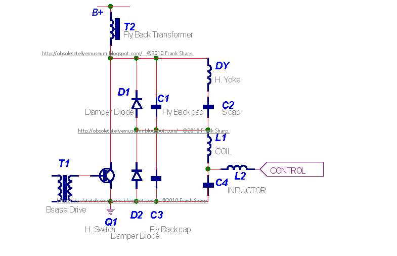 SPLIT DIODE MODULATOR
This horizontal circuit consists of two parts. D1, C1, C2 and DY are the components as described above.
D2, C3, C4 and L1 are a second “dummy” horizontal section that does not cause deflection current. By the
D.C. analyzing this circuit the voltage across C2 + C4 must equal the supply voltage (B+). Deflection
current in the DY is related to the supply voltage minus the voltage across C4. For a maximum horizontal
size the control point must be held at ground. This causes the dummy section to not operate and the DY
section will get full supply voltage. If the control point is at 1/3 supply then the DY section will be
operating at 2/3 supply.
Note: The impedance of (D1,C1,C2 and DY) and (D2,C3,C4 and L1) makes a voltage divider. If the
control point is not connected then there is some natural voltage on C4. Most split diode monitors are built
to pull power from the dummy section through L2 to ground. A single power transistor shunts from the
control point to ground. It is true that power can be supplied from some other supply through L2 to rise the voltage on C4. For maximum range a bi-directional power amplifier can drive the control point.
The most exciting feature if the split diode modulator is that the flyback pulse, as seen by the flyback
transformer, is the same size at all horizontal size settings.
HORIZONTAL SWITCH/DAMPER DIODEOn the right hand side of the screen, the H. switch transistor conducts current through the deflection yoke.
This current comes from the S correction capacitors, which have a charge equal to the effective supply
voltage. The damper diode allows current for the left hand side of the screen to flow back through the
deflection yoke to the S capacitors.
FLYBACK CAPACITOR
The flyback capacitor connects the hot side of the yoke to ground. This component determines the size and
length of the flyback pulse. ‘Tuning the flyback capacitor’ is done to match the timing of the flyback pulse
to the video blanking time of the video signal. The peak flyback voltage on the horizontal switch must be
set to less that 80% if the Vces specification. The two conditions of time and voltage can be set by three
variables (supply voltage, retrace capacitor and yoke inductance) .
S CAPACITOR
The S capacitors corrects outside versus center linearity in the horizontal scan. The voltage on the S cap
has a parabola plus the DC horizontal supply. Reducing the value of S cap increases this parabola thus
reducing the size of the outside characters and increasing the size of the center characters.
S Capacitor value: Too low: picture will be squashed towards edges.
Too high: picture will be stretched towards edges.
By simply putting a capacitor in series with each coil, the sawtooth waveform ismodified into a slightly sine-wave shape. This reduces the scanning speed near the
edges where the yoke is more sensitive. Generally the deflection angle of the electron
beam and the yoke current are closely related. The problem is the deflection angle
verses the distance of movement on the CRT screen does not have a linear effect.
BASE DRIVE CURRENT
The base drive resistor determines the amount of
base drive. If the transistor is over driven the Vsat
looks very good, but the current fall time is poor.
If the base current is too small the current fall time is very fast. The problem is that the transistor will have many volts across C-E when closed.
The best condition is found by placing the transistor in the heaviest load condition. Adjust the base resistor for the least power consumption then increase the base drive a small amount. This will slightly over drive the base.
BU208(A)
Silicon NPNnpn transistors,pnp transistors,transistors
Category: NPN Transistor, Transistor
MHz: <1 MHz
Amps: 5A
Volts: 1500V
HIGH VOLTAGE CAPABILITY
JEDEC TO-3 METAL CASE.
DESCRIPTION
The BU208A, BU508A and BU508AFI are
manufactured using Multiepitaxial Mesa
technology for cost-effective high performance
and use a Hollow Emitter structure to enhance
switching speeds.
APPLICATIONS:
* HORIZONTAL DEFLECTION FOR COLOUR TV With 110° or even 90° degree of deflection angle.
ABSOLUTE MAXIMUM RATINGS
Symbol Parameter Value Unit
VCES Collector-Emit ter Voltage (VBE = 0) 1500 V
VCEO Collector-Emit ter Voltage (IB = 0) 700 V
VEBO Emitter-Base Voltage (IC = 0) 10 V
IC Collector Current 8 A
ICM Collector Peak Current (tp < 5 ms) 15 A
TO - 3 TO - 218 ISOWATT218
Ptot Total Dissipation at Tc = 25 oC 150 125 50 W
Tstg Storage Temperature -65 to 175 -65 to 150 -65 to 150 oC
Tj Max. Operating Junction Temperature 175 150 150 °C


Chassis F6TT UNITS view.
- Luminance + Chrominance unit 492.045 G8 with TDA2500/3 + TDA2522 (all PHILIPS)
(Note the long luminance delay line)
- Synchronization Unit with TDA2593 (PHILIPS) 492.174 G10
- Sound - Audio Unit with TBA120U (Telefunken) + L130V (Fairchild Semiconductors) 492.044/E3
- RGB Amplifiers with TBA530 (PHILIPS) 943/K7
- Frame deflection unit 492.225/C1
- E/W Correction Unit 492.213/C
TDA2522 PAL TV CHROMA DEMODULATOR COMBINATION
FAIRCHILD LINEAR INTEGRATED CIRCUIT
GENERAL DESCRIPTION- The TDA2522 is a monolithic integrated circuit designed as
a synchronous demodulator for PAL color television receivers. It includes an 8,8 MHz

oscillator and divider to generate two 4.4 MHz reference signals and provides color difference outputs.
PACKAGE OUTLINE 9B
The TDA2522 is Intended to Interface directly with the TDA2560 with a minimum oF external components. The TDA2530 may be added if RGB drive is required. The TDA2522
is constructed using the Fairchild Planar* process.
TDA2520 COLOUR DEMODULATOR COMBINATION
The TDA2520 is an integrated synchronous demodulator combination for colour television
receivers incorporating the following functions :

~ 8, 8 MHZ oscillator followed by a divider giving two 4, 4 MHZ signals used as reference
signals
- keyed burst phase detector for optimum noise behaviour
- a stage to obtain chrominance signal control (a. c. c.) and an a. c. c. reference level
- a colour killer and identification signal detector
- two synchronous demodulators for the (B-Y) and (R-Y) signals
- temperature compensated emitter follower outputs
- PAL switch
- PAL flip-flop
- integrated capacitors in the symmetrical demodulators reduce unwanted carrier-
signals at the outputs.
TDA2593 SYNCHRO AND HORIZONTAL DEFLECTION CONTROL FOR COLOR TV SETDESCRIPTION
The TDA2593 isa circuit intended for the horizontal
deflectionof color TVsets, suppliedwith transistors
or SCR’S.
.LINE OSCILLATOR(two levels switching)
.PHASE COMPARISON BETWEEN SYNCHRO-
PULSE AND OSCILLATOR VOLTAGE
Ø 1, ENABLED BY AN INTERNAL PULSE,
(better parasitic immunity)
.PHASE COMPARISON BETWEEN THE FLYBACK
PULSES AND THE OSCILLATORVOLTAGE
Ø2
.COINCIDENCE DETECTOR PROVIDING A
LARGE HOLD-IN-RANGE .FILTER CHARACTERISTICS AND GATE
SWITCHING FOR VIDEO RECORDER APPLICATION
.NOISE GATED SYNCHRO SEPARATOR
.FRAME PULSE SEPARATOR
.BLANKING AND SAND CASTLE OUTPUT
PULSES
.HORIZONTAL POWER STAGE PHASE LAGGING
CIRCUIT
.SWITCHING OF CONTROL OUTPUT PULSE
WIDTH
.SEPARATED SUPPLY VOLTAGE OUTPUT
STAGE ALLOWING DIRECT DRIVE OF
SCR’S CIRCUIT .SECURITY CIRCUIT MAKES THE OUTPUT
PULSE SUPPRESSED WHEN LOW SUPPLY
VOLTAGE.


NORDMENDE SPECTRA COLOR TP9762 Chassis F6TT Power Supply view.
SMPS supply with S2530A (TOSHIBA) Chassis F6TT Power Supply view.
- Tuning Unit 596.156
- TUNING OSD BAR DURING SEARCH UNIT 592.137
- PROGRAM MEMORY + A/D VST SYNTH 492.120
- ULTRASONIC AQUIRING / DETECTOR / AMPL 592.155
TDA2541 IF AMPLIFIER WITH DEMODULATOR AND AFC

.SUPPLYVOLTAGE : 12V TYP .SUPPLYCURRENT : 50mATYP .I.F. INPUT VOLTAGE SENSITIVITY AT
F = 38.9MHz : 85mVRMS TYP .VIDEO OUTPUT VOLTAGE (white at 10% of
top synchro) : 2.7VPP TYP .I.F. VOLTAGE GAIN CONTROL RANGE :
64dB TYP .SIGNAL TO NOISE RATIO AT VI = 10mV :
58dB TYP .A.F.C. OUTPUT VOLTAGE SWING FOR
Df = 100kHz : 10V TYP
DESCRIPTION
The TDA2540 and 2541 are IF amplifier and A.M.
demodulator circuits for colour and black and white
television receiversusing PNP or NPNtuners. They
are intended for reception of negative or positive
modulation CCIR standard.
They incorporate the following functions : .Gain controlled amplifier .Synchronous demodulator .White spot inverter .Video preamplifier with noise protection .Switchable AFC .AGC with noise gating .Tuner AGC output (NPN tuner for 2540)-(PNP
tuner for 2541) .VCR switch for video output inhibition (VCR
play back)
TDA2590 horizontal oscillator combination
GENERAL DESCRIPTION
— The TDA2590 is a monolithic integrated circuit designed
as a horizontal oscillator combination for TV receivers and monitors.

It is constructed using the Fairchild Planar* process.
LINE OSCILLATOR USING THE THRESHOLD SWITCHING PRINCIPLE
PHASE COMPARISON BETWEEN SYNC PULSE AND OSCILLATOR VOLTAGE (d>1)
PHASE COMPARISON BETWEEN LINE FLYBACK PULSE AND OSCILLATOR VOLTAGE
(<62) Y
SWITCH FOR CHANGING THE FILTER CHARACTERISTIC AND THE GATE CIRCUIT
{WHEN USED FOR VCR)
COINCIDENCE DETECTOR (¢3)
SYNC SEPARATOR
NOISE SEPARATOR
VERTICAL SYNC SEPARATOR AND OUTPUT STAGE
COLOR BURST KEYING AND LINE FLYBACK BLANKING PULSE GENERATOR
PHASE SHIFTER FOR THE OUTPUT PULSE
OUTPUT PULSE DURATION SWITCHING
OUTPUT STAGE FOR DIRECT DRIVE OF THYRISTOR DEFLECTION CIRCUITS
SYNC GATING PULSE GENERATOR
LOW SUPPLY VOLTAGE PROTECTION.
ULTRASONIC REMOTE CONTROL RECEIVER NORDMENDE SPECTRA COLOR TP9762 CHASSIS F6TT
An ultrasonic remote control receiver wherein an incoming ultrasonic signal is converted to square wave pulses of the same frequency by a Schmitt trigger circuit; digital circuits are thereafter used to count pulses resulting from the incoming signal over a predetermined period of time; a decoder activates one of a plurality of outputs in dependance to the number of pulses counted, provision is made to prevent interference signals from producing undesired control outputs.

1. An ultrasonic remote control receiver for applying a control signal to a selected one of a plurality of control channels in response to and dependent on the frequency of a received ultrasonic signal comprising:
2. An ultrasonic remote control receiver comprising:
3. An ultrasonic remote control receiver comprising:
4. The ultrasonic remote control receiver as defined in claim 3, wherein said means producing square pulses is a Schmitt trigger circuit and said means providing a signal input to said sequence controller is a retriggerable monostable multivibrator.
5. An ultrasonic remote control receiver comprising:
6. An ultrasonic remote control receiver comprising:
7. An ultrasonic remote control receiver as defined in claim 6 further comprising a monostable multivibrator between the output of said Schmitt trigger circuit and the remaining elements of said receiver.
8. An ultrasonic remote control receiver as defined in claim 6 further comprising a bistable multivibrator between the output of said Schmitt trigger circuit and the remaing elements of said receiver.
9. The ultrasonic remote control receiver as defined in claim 7 wherein the hold period of said monostable multivibrator is slightly less than one half the period of said square wave pulses from said Schmitt trigger circuit.
Description:
The invention relates to an ultrasonic remote control receiver for receiving signals having different useful frequencies each associated with a channel, comprising a plurality of outputs which are each associated with one of the channels and from which a control signal is emitted on receipt of a signal having the corresponding useful frequency.To obtain the simplest possible transmitter construction in ultrasonic remote control, modulation of the emitted ultrasonic frequencies is not employed; to control different operations different frequencies are emitted which must be recognized in the receiver and evaluated for carrying out the different functions associated therewith. Presently, to recognize the different frequencies, use is made of resonant circuits, each of which contains one or more coils tuned in each case together with a capacitor to one of the useful frequencies.
These hitherto known receivers have numerous disadvantages. Thus, for example, before starting operation of the receiver a time-consuming alignment procedure must be carried out with which the resonant frequencies of the individual resonant circuits are set. Since it is inevitable that with time the resonant circuits become detuned, it may be necessary to repeat the alignment procedure.
A further disadvantage is that the known receivers cannot be made by integrated techniques because the coils used therein are not suitable for such techniques.
The problem underlying the invention is thus to provide an ultrasonic remote control receiver of the type mentioned at above which is extremely simple to set and in addition can be made by integrated techniques.
To solve this problem, according to the invention an ultrasonic remote control receiver of the type mentioned above contains a counter for counting the useful frequency oscillations received during a fixed measuring time, a sequence control device which determines the measuring time and which is started on receipt of a useful frequency, and a decoder comprising several outputs which is connected to the outputs of the counter, said decoder emitting a control signal at the output associated with the count reached at the end of the measuring time.
In the receiver constructed according to the invention the frequency emitted by the transmitter is identified by counting the oscillations received during a measuring time. The evaluation of the count reached at the end of the measuring time takes place in a decoder which emits a control signal at a certain output according to the count. The measuring time is fixed by a sequence control device which is set in operation on receipt of useful frequency signals.
In such a receiver the only quantity which has to be exactly fixed is the measuring time; it is therefore no longer necessary to align components to certain frequencies. Since no coils are required, the novel receiver can also be made up of integrated circuits.
A further development of the invention resides in that an interference identifying device is provided which on receipt of interference frequencies differing from the useful frequencies interrupts the operation of the sequence control device.
Hitherto known ultrasonic remote control receivers respond to any oscillation received if the frequency thereof has a value which excites a resonant circuit in the receiver. There is no way of distinguishing between oscillations received from the remote control transmitter and from interference sources.
Interfering ultrasonic oscillations may be due to many different causes. For example, noises such as hand clapping, rattling of short keys such as safety keys, operating cigarette lighters, rattling of crockery and the like cover a frequency spectrum reaching from the audio frequency range far into the ultrasonic region. The ultrasonic components may have the effect of simulating a useful frequency and cause an erroneous function in the receiver.
The interference identifying device according to the further development is constructed in such a manner that it recognizes oscillations having frequencies deviating from the useful frequencies and as a result of this recognition switches off the sequence control device. This switching off prevents the counter state reached from being passed to the decoder and consequently the latter cannot emit an erroneous control signal.
With this further development of the ultrasonic remote control receiver the operation of equipment such as radio and television sets is made extremely reliable and interference-free. During the operation of such a set it is no longer possible for the remote control to become operative, triggered by interference noises, eliminating for example the possibility of unintentional program or volume changes.
Examples of embodiment of the invention are illustrated in the drawings, wherein:
FIG. 1 shows a block circuit diagram of a remote control receiver according to the invention;
FIG. 2 is a diagram explaining the mode of operation of the circuit according to FIG. 1;
FIG. 3 shows another embodiment of the invention;
FIG. 4 is a diagram explaining the mode of operation of the circuit according to FIG. 3;
FIG. 5 is a diagram illustrating interference frequency identification in the circuit according to FIG. 3;
FIG. 6 shows a block circuit diagram of another embodiment of part of the circuit according to FIG. 3;
FIG. 7 is a diagram explaining the mode of operation of the embodiment according to FIG. 6;
FIG. 8 is a block circuit diagram of a further embodiment of a part of the circuit according to FIG. and, an
FIG. 9 is a diagram explaining the mode of operation of the embodiment according to FIG. 8.
 The ultrasonic remote control receiver shown in FIG. 1 comprises an input 1 which is connected to an ultrasonic microphone intended to receive ultrasonic signals coming from a remote control transmitter. For each function to be performed by the receiver the remote control transmitter emits one of several unmodulated different useful frequencies which are spaced from each other a constant channel spacing Δ f and which all lie within a useful frequency band.
To obtain a signal which is as free as possible from noise at the input 1, a band filter and a limiting amplifier are preferably incorporated between the ultrasonic microphone and the input 1. The band filter may be made up of two active filters whose resonant frequencies are offset with respect to each other so that a pass band curve in the useful frequency band is obtained which is as flat as possible.
The input 1 leads to a Schmitt trigger 2 which converts the electrical signal applied thereto with the frequency of the ultrasonic signal to a sequence of rectangular pulses. The output 3 of the Schmitt trigger 2 is connected to the input 6 of a frequency divider 7 which is in operation for the duration of a control pulse applied to its control input 8 and divides the recurrence frequency of the pulses supplied thereto at the input 6 thereof in a constant division ratio. The output 9 of the frequency divider 7 is connected to the input 10 of a counter 11 which counts the pulses coming from the frequency divider 7. The counter 11 is a four-stage binary counter whose stage outputs are connected to the inputs of a store (register) 12 which is so constructed that on application of a control pulse to the input 12 thereof it takes on the counter state in the counter 11 and stores said counter state until the next pulse at the input 13. The stage outputs of the store 12 are fed to the inputs of a decoder 14 which decodes the counter state contained in the store 12 in such a manner that a control signal is emitted at that one of its outputs D0 to D9 which is associated with the decoded counter state.
The output 3 of the Schmitt trigger 2 is also connected to the input 4 of a monoflop 5 which is brought into its operating state by each pulse at the output 3 of the Schmitt trigger. It returns from this operating state to its quiescent state after expiration of a hold time depending on its intrinsic time constant if it does not receive a new pulse prior to expiration of this hold time. It is held in the operating state by each pulse received during the hold time until it finally flops back into the quiescent state when the interval between two successive pulses is greater than its hold time.
The output 15 of the monoflop circuit 5 is connected to the input 16 of a sequence control device 17 which is set in operation by the signal emitted in the operating state of the monoflop 5. Supplied to the sequence control device by 17 via a Schmitt trigger 18 at a control input 19 are pulses having a recurrence frequency derived from oscillations of the same frequency, for example, twice the mains frequency of 100 c/s, applied to the input 20. The sequence control device 17 is so constructed that in a cyclically recurring sequence in time with the pulses supplied to it at the input 19 it emits pulses at the outputs 21, 22 and 23 whose duration is equal to the period of the oscillation applied to the input 20. The output 21 of the sequence control device 17 is connected to the control input 8 of the frequency divider 7, the output 22 is connected to the control input 13 of the store 12 and the output 23 thereof is connected to the reset input 24 of the counter 11.
The mode of operation of the circuit of FIG. 1 will now be explained with the aid of the diagram of FIG. 2
 which shows the variation with time of the signals at the output 3 of the Schmitt trigger 2 and at the inputs 16 and 19 as well as the outputs 21, 22 and 23 of the sequence control device 17.
It will be assumed that a useful frequency oscillation is being received at the input 1. The Schmitt trigger 2 then emits at the output 3 rectangular pulses whose recurrence frequency is equal to the frequency of said useful frequency oscillation. The first pulse emitted by the Schmitt trigger 2 puts the monoflop 5 into its operating state. The hold time of the monoflop 5 is so dimensioned that for all useful frequencies occurring it is longer than the recurrence period of the rectangular pulses emitted at the output 3. The monoflop 5 therefore remains in its operating state for as long as the useful frequency oscillation is applied to the input 1 and supplies to the control input 16 of the sequence control device 17 a control signal throughout this time.
Due to the control signal applied to the input 16 the sequence control device 17 emits at its outputs 21, 22 and 23 in time with the pulses supplied to it via the Schmitt trigger 18 at the input 19 mutually offset control pulse sequences, the duration of the control pulses being equal to the time interval of the leading edges of the pulses supplied at the input 19 and thus equal to the period of the oscillation applied to the input 20 and the pulse sequences being offset with respect to each other by one pulse duration. The control pulses emitted by the sequence control device 17 perform the following functions:
a. The first control pulse appearing at the output 21 sets in operation for its duration via the input 8 the frequency divider 7 so that the latter divides the recurrence frequency of the pulses supplied thereto from the Schmitt trigger 2 and thus the frequency of the useful frequency oscillations received in a constant ratio and passes counting pulses to the input 10 of the counter 11 with a correspondingly reduced recurrence frequency.
b. Via the input 13 the second pulse occurring at the output 22 causes the store 12 to take on and to store the count of the counter 11 reached at the end of the first control pulse.
c. The third control pulse appearing at the output 23 resets the counter 11 via the reset input 24.
COntrol pulse sequences continue to be emitted for as lon
g as the monoflop 5 remains in its operating state.Since the stage outputs of the store 12 are permanently connected to the inputs of the decoder 14, the store content is continuously being decoded. The decoder 14 therefore emits a control signal at the output which is associated with the count contained in the store.
During each group of three offset control pulses of the three control pulse sequences emitted by the sequence control device 17, the counter 11 receives counting pulses from the frequency divider 8 only for the duration of the control pulse of the first control pulse sequence emitted at the output 21. The duration of this control pulse thus determines the measuring time during which the oscillations of the useful frequency signal received are counted. Since the duration of the control pulses emitted by the sequence control device 17 is however equal to the period of the oscillation applied to the input 20, the measuring time is fixed by the period of said oscillation.
The frequency divider 7 is connected in front of the counter 11 so that a small capacity of the counter 11 is sufficient to obtain a clear indication of the received frequency even when the measuring time is so long that a large number of periods of the useful frequency oscillation is received during the measuring time. This is for example, the case when the oscillation supplied to the input 20 has twice the mains frequency. Since the frequency divider 7 divides the frequency of the useful frequency oscillations received in the constant ratio k, the counter 11 need count only the oscillations having a correspondingly reduced frequency. If the division ratio k of the divider 7 is so set that it is equal to the product of the measuring time t and channel spacing Δ f, only a frequency which differs by at least the channel spacing Δ f from a previously received frequency will change the count of the counter 11.
The purpose of the monoflop 5 is to prevent interference frequencies supplied to the input 1 from producing at one of the outputs D0 to D9 of the decoder 14 a control signal which could lead to an erroneous function of the equipment being controlled. The interference sources usually encountered emit a frequency spectrum whose components lie predominantly in the audio region, i.e., below the ultrasonic region. If the hold time of the monoflop 5 is set to a value slightly greater than the period of the smallest useful frequency but smaller than the period of the highest interference frequency occurring, the monoflop 5 returns to its quiescent state before the end of the period of an interference frequency. Since in this state no signal is supplied to the control input 16 of the sequence control device 17, the latter is put out of operation and consequently the received signal cannot be evaluated because the count of the counter 11 is not transferred to the store 12 and thus no decoding takes place.
To facilitate understanding of the invention, the function of the circuit of FIG. 1 will now be explained numerically by way of example. The channel spacing Δ f will be taken as 1,200 c/s so that for a frequen
cy of 100 c/s of the oscillation applied to the input 20 and thus a measuring time of 10 ms a division ratio of the frequency divider 7 of k = t . Δf = 12 results. It will further be assumed that ten different channel frequencies are to be evaluated; the counter 11 is therefore so connected that it has a capacity of 10. With these values, during the measuring time the counter 11 runs through several count cycles. This means that for the received frequency during the measuring time the counter 11 reaches its maximum count several times and then starts counting again from the beginning. The count reached at the end of the measuring time is however still a clear indication of the received useful frequency provided the number of useful frequencies having a channel spacing Δf is at the most equal to the counter capacity Z. The relationship between the useful frequency f received and the count reached at the end of each measuring time t while this useful frequency is being received is expressed by the following equation:f = (k/t) . (n . Z + m + 0.5)
wherein
f = useful frequency received in c/s
t = measuring time in seconds
k = division ratio of the frequency divider 7
Z = capacity of the counter 11
n = number of count cycles passed through (integral)
m = count
The term 0.5 in brackets is a correction factor which ensures that a new count is reached whenever the received frequency differs at least by half the channel spacing Δf from the channel center frequency of the neighboring channel. With a channel spacing Δ of 1,200 c/s, a measuring time t of 10 ms, a division ratio k of the frequency divider 7 of 12, a capacity Z of the counter 11 of 10 and an input frequency f of 33 k c/s, the count 7 is for example reached after two complete count cycles. This is because the input frequency of 33 k c/s is first divided by 12 by the frequency divider 7 so that pulses having a recurrence frequency of 2.750 k c/s reach the input 10 of the counter 11. Since the frequency divider 7 emits counting pulses only during the measuring time of 10 ms, during said time only 27.5 pulses reach the input 10 of the counter 11. For this number of pulses the counter thus runs through two complete cycles and finally stops at the count 7. Similarly, for an input frequency of 39 k c/s the counter stops at the count 2 after passing through three complete counter cycles. With the numerical values given up to 10 different frequencies may be received without any ambiguity occurring in the evaluation.
FIG. 3 illustrates a further embodiment of an ultrasonic remote control receiver which differs from the embodiment described above primarily in that to fix the measuring time it is not necessary to supply a reference frequency.
 In the illustration of FIG. 3 the same reference numerals as in FIG. 1 are used for identical circuit components. The part of the circuit enclosed in the dashed line represents the sequence control device 17' which emits at its outputs 21', 22', 23' control signals which have substantially the same functions as the control signals emitted at the outputs 21, 22 and 23 of the sequence control device 17 of FIG. 1.
The useful frequency signal received is again supplied to the input 1. The input 1 is connected to the input of the Schmitt trigger 2 which again converts the input useful frequency oscillations into a sequence of pulses whose recurrence frequency is equal to the input useful frequency. The output 3 of the Schmitt trigger 2 is connected to the input B1 of a monoflop 25 which is contained in the sequence control device 17' and which is so constructed that it is switched to its operating state by a pulse received at the input B1 but during its hold time cannot be tripped again by any further pulse. The output 3 of the Schmitt trigger 2 is also connected to the input 26 of an AND gate 27 whose other input 28 is connected to that output 21' of the sequence control device 17' which is directly connected to the output Q1 of the monoflop 25. The output Q1 of the monoflop 25 which emits the signal complementary to the signal at the output Q1 is connected to the input B2 of a further monoflop 29 whose output Q2 is connected to the input A1 of the monoflop 25. The input 10 of the counter 11 is connected to the output of the AND gate 27. The stage outputs of the counter 11 are connected to the inputs of a gate circuit 30 which on receipt of a control pulse at its input 31 transfers the count contained in the counter 11 to the decoder 14 connected to its outputs. In the decoder 14 the count is then decoded in the manner already explained in conjunction with FIG. 1 so that a control signal is emitted at the output corresponding to the transferred count.
The output 3 of the Schmitt trigger 2 is further connected to the input 32 of an AND gate 33 which is contained in the sequence control circuit 17' and the other input 34 of which is connected to the output of a NOR gate 35. The output Q1 of the monoflop 25 is directly connected to one input 36 of the NOR gate 35 and is connected to the other input 37 via a delay member 38 and an inverter 39.
The output of the AND gate 33 represents the output 22' of the sequence control circuit 17' which is directly connected to the control input 31 of the gate circuit 30. In addition, the output of the AND gate 33 is directly connected to one input 40 of a NOR gate 41 and to the other input 42 thereof via a delay member 43 and an inverter 44. The output of the NOR gate 41 represents the output 23' of the sequence control circuit 17', to which output the reset input 24 of the counter 11 is connected.
The mode of operation of the circuit of FIG. 3 is explained in FIG. 4. Since the measuring time in the arrangement of FIG. 3 is substantially shorter than in the arrangement of FIG. 1, the time scale in FIG. 4
 has been enlarged compared with FIG. 2 in order to clarify the illustration. When useful frequency oscillations are supplied to the input 1 of the receiver, pulses whose recurrence frequency is equal to the useful frequency appear at the output 3 of the Schmitt trigger 2. It will be assumed that the presence of a pulse corresponds to the logical signal value 1 whereas a pulse space represents the logical signal value 0. The leading edge of the first pulse at the output 3 puts the monoflop 25 into its operating state in which it emits the signal value 1 for the duration of its hold time at its output Q1, resulting in the control pulse at the output 21', which passes to the input 28 of the AND gate 27. Since the other input 26 of the AND gate 27 is directly connected to the output 3 of the Schmitt trigger 2, for the duration of each pulse at the output 3 the signal value 1 is also applied to the input 26 of the AND gate 27. Thus, the pulses occurring at the output 3 of the Schmitt trigger 2 are transferred for the duration of the control pulse at the output 21', i.e. during the hold time of the monoflop 25, as count pulses to the counter 11 and counted by the latter. The hold time of the monoflop 25 thus determines the measuring time; the capacity of the counter 11 must be greater than the number of pulses received during the measuring time for the greatest useful frequency. The count of the counter 11 reached at the end of the measuring time is then a clear indication of the received useful frequency.
When the monoflop 25 flops back into the quiescent state at the end of its hold time, it applies the signal value 0 via its output Q1 to the input 28 of the AND gate 27 so that no further count pulses can enter the counter 11. At the same time there appears at the output Q1 of the monoflop 25 the signal value 1 which at the input B2 puts the monoflop 29 into the operating state. In this state the monoflop 29 emits at its output Q2 the signal value 1 which blocks the monoflop 25 via the input A1 for the duration of the hold time of the monoflop 29 in such a manner that it cannot be switched into the operating state by pulses at the input B1. This is necessary to enable the sequence control device 17' to have sufficient time to generate the control pulses appearing at the outputs 22' and 23' for the transfer of the count or resetting of the counter.
With the return of the monoflop 25 to its quiescent state, the signal value 0 passes to the input 26 of the NOR gate 35 directly connected to the output Q1. During the operating state of the monoflop 25 the signal value 0 is applied with a delay determined by the delay member 38 via the inverter 39 to the input 37 of the NOR gate 35, said signal value 0 being replaced by the signal value 1 only after the delay time of the delay member 38 and not simultaneously with the flop back of the monoflop 25. Thus, for the duration of this delay time the signal value 0 is applied to both inputs 36 and 37 of the NOR gate 35 and consequently for this period of time the signal value 1 appears at the output of the NOR gate 35. The circuits 35, 38, 39 thus effect the generation of a short pulse which immediately follows the return of the monoflop 25 and the duration of which is determined by the delay of the delay member 38. This pulse is applied to the input 34 of the AND gate 33 (FIG. 4). The same effect could obviously alternatively be obtained with a monoflop which is tripped by the signal at the output Q1 changing from the value 1 to the value 0.
Now, if during this time a pulse is emitted at the output 3 of the Schmitt trigger 2, i.e., a signal value 1 is at the input 32 of the AND gate 33, said gate supplies to the control input 31 of the gate circuit 30 a control pulse for the duration of the delay of the delay member 38. This control pulse opens the gate circuit so that it allows the count reached at the end of the hold time of the monoflop 25 to pass to the decoder 14. The latter then emits a control signal at the output associated with this count. The signal value 1 present at the output of the AND gate 33 during the delay of the delay member 38 also passes directly to the input 40 of the NOR gate 41, at the other input 42 of which the signal value 0 is applied for the duration of the same pulse but with a delay determined by the delay member 43. Thus, in a manner similar to the circuits 35, 38, 39 the circuits 41, 43, 44 produce a short pulse which immediately follows the end of the output pulse of the AND gate 33 and appears at the output 23' of the sequence control circuit and is applied to the reset input 24 of the counter 11 (FIG. 4). This pulse resets the counter 11.
The hold time of the monoflop 29 is so set that it flops back into its quiescent state again only when the transfer process from the counter to the decoder via the gate circuit and the resetting of the counter has been effected. When the monoflop 29 returns to its quiescent state, it emits at its output Q2 the signal value 0 which brings the monoflop 25 via the input A1 thereof into such a condition that it can again be brought into its operating state by a pulse at the output 3 of the Schmitt trigger 2. In this manner the measuring and evaluating periods can be repeated for as long as useful frequency oscillations are supplied to the input 1.
In the circuit according to FIG. 3, interference frequencies are suppressed by setting a certain hold time of the monoflop 25. It is apparent from the above description of the function that the transfer of the count of the counter 11 to the decoder 14 takes place immediately following the end of the hold time of the monoflop 25, i.e., immediately following the end of the measuring time. However, a control signal initiating the transfer can be applied by the AND gate 33 to
the control input 31 of the gate circuit 30 only when simultaneously with the end of the measuring time a pulse, i.e., the signal value 1, is present at the output 3 of the Schmitt trigger 2. Now, if the hold time of the monoflop 25 is made equal to the reciprocal of the channel spacing Δf, this coincidence at the AND gate 33 at the end of the measuring time occurs only when quite definite frequencies are applied to the input 1; these frequencies lie only within frequency bands which in the example described here, in which the output pulses of the Schmitt trigger 2 have a pulse duty factor of 1:2, have the width of half a channel spacing. These frequency bands each contain one of the useful frequencies. Between these frequency bands there are gaps having the width of half the channel frequency and frequencies falling in these gaps do not produce coincidence at the AND gate 33 and consequently cannot be evaluated by transfer of the count of the counter 11 to the decoder 14. Thus, frequency windows are formed over the entire frequency range which can occur at the input 1 and only frequencies lying within these windows are treated by the circuit according to FIG. 3 as useful frequencies. All intermediate frequencies are recognized as interference frequencies and excluded from evaluation.If the measuring time is made exactly equal to the reciprocal of the channel spacing the frequency bands in which evaluation takes place are such that the rated frequencies of the signals transmitted by the transmitter are disposed at the lower end of the frequency bands. Thus, in this case only frequencies starting from a rated frequency in each case and extending up to the frequency in the center between two channels would be evaluated as useful frequencies. Since the frequency of the signals emitted by the transmitter can however also fluctuate below the rated frequency, it is desirable to place the frequency bands in which evaluation takes place so that the rated frequencies lie substantially in the center of the bands. To achieve this, the hold time of the m
onoflop 25 and thus the measuring time is lengthened by a quarter of the reciprocal of the maximum rated frequency. Although with this setting only the maximum rated frequency lies exactly in the center of the corresponding frequency band, the other rated frequencies still lie within the corresponding frequency bands and consequently the frequencies of the useful signals can also deviate from the rated frequency downwardly without preventing evaluation. The frequency gaps including the frequencies treated as interference frequencies then lie in each case substantially in the center between two rated frequencies.To facilitate understanding of the type of interference identification just outlined attention is drawn to FIG. 5;
 the latter shows at Q1 the output signal of the monoflop 25 determining the measuring time, at 3-F1, 3-F2, 3-F3 the pulse sequences appearing at the output 3 of the Schmitt trigger 2 for three different useful frequencies F1, F2, F3 and at 3-FS the pulse sequence which appears at the output 3 when an interference frequency FS is received which lies between the useful frequencies F2 and F3. It is apparent from this diagram that at the end of the measuring time a pulse is present at the output 3 of the Schmitt trigger only when useful frequencies are being received and that when an interference frequency is applied there is a pulse space at the end of the measuring time. Thus, at the AND gate 33 the presence of a pulse at the end of the measuring time is employed as criterion for the receipt of a useful frequency. It is also apparent from FIG. 5 that with the useful frequency F1 the counter 11 counts 4 pulses, with the useful frequency F2 up to 5 pulses and with the useful frequency F3 6 pulses.
Isolated short interference pulses which could reach the input 1 of the circuit of FIG. 3 between two useful pulses and undesirably increase the count may be made ineffective by inserting a flip-flop circuit 45 between the output 3 of the Schmitt trigger 2 and the rest of the circuit as illustrated in FIG. 6.
 The mode of operation of this flip-flop circuit 45 will be explained with the aid of FIG. 7, which shows the signals at the output 3 of the Schmitt trigger 2 and at the output 3a of the flip-flop circuit 45 firstly without interference and secondly with interference. The flip-flop circuit 45 is tripped by the leading edge of each output pulse of the Schmitt trigger 2. If a short interference pulse is received, the flip-flop circuit 45 supplies at its output 3a the signal value 0 for example on receipt of the useful pulse preceding the interference pulse, the signal value 1 on receipt of the interference pulse and the signal value 0 on receipt of the next useful pulse. If no interference pulse had occurred, the flip-flop circuit would not have been switched to the signal value 1 at the output until receipt of the next useful pulse. The flip-flop circuit thus effects on receipt of an interference pulse (and in general on receipt of an odd number of interference pulses) between two useful pulses a reversal of the signal values so that at the end of the measuring time coincidence is not reached at the gate 33 although a useful frequency was received. Without the flip-flop circuit 45 the count would be transferred, although because of the interference pulse received it would not correspond to the useful frequency received.
The embodiment of FIG. 3 differs from the embodiment of FIG. 1 also in that instead of the store (register) 12 the gate circuit 30 is used that allow the count to be evaluated to pass briefly only once in a measuring and evaluating time. Thus, at the output of the decoder 14, instead of a uniform signal as in the case of the embodiment of FIG. 1, a series of pulses appears with the spacing of the control signals at the input 31 of the gate circuit 30. The use of a gate circuit instead of a store is suitable in applications where the equipment to be controlled must be actuated with control pulses and not with a uniform signal.
The immunity to interference may be further increased if in accordance with FIG. 8
 a further monoflop 46 which cannot be triggered again during its hold time is inserted between the output 3 of the Schmitt trigger 2 (or the output 3a of the flip-flop circuit 45 of FIG. 6) and the remainder of the circuit. This hold time is set to half the period of the highest useful frequency. This modification is effective against a particular type of interferences, i.e., cases where an amplitude break occurs within an oscillation at the input 1 of the Schmitt trigger 2; this break would lead at the output 3 of the Schmitt trigger to the emission of two pulses instead of the single pulse per oscillation emitted in the normal case. These two pulses give the same effect as the receipt of a frequency which is twice as high and consequently without the additional monoflop 46 erroneous evaluations could arise. However, the monoflop 46 prevents the two pulses from becoming separately effective because it always emits pulses having the duration of its hold time; short double pulses which can arise due to amplitude breaks in the received signal thus cannot have any effect. FIG. 9 shows the action of the monoflop 46 when an amplitude break occurs at the input 1 of the Schmitt trigger 2 which produces a double pulse at the output 3 of the Schmitt trigger. As is apparent, the pulses at the output 3b of the monoflop 46 are not affected by this double pulse.
One embodiment of the remote control receiver may also reside in that a sequence control counter fed by the pulses at the output of the Schmitt trigger 18 is used for the sequence control device 17 of FIG. 1; the stage outputs of said counter are connected to a decoder which is so designed that it activates one after the other one of its outputs for each count. Thus, for example, this decoder may have 10 outputs which are activated successively in each counting period of the sequence control counter. Since in accordance with the description of the example of embodiment of FIG. 1 a total of three control signals are required for the evaluation of the frequency received, the output signals at the fourth, fifth and seventh outputs may be used respectively for activating the freque
ncy divider 7, opening the store 12 and resetting the counter 11. Since in this case the evaluation of the received frequency by the control pulses emitted from the output of the decoder of the sequence control device does not begin until the decoder emits a signal at its fourth output, there is an evaluation delay which has the advantage that short interference pulses produce no response in the receiver.The advantageous formation of frequency band windows are used in the embodiment of FIG. 3 can also be applied in the embodiment of FIG. 1 if instead of the retriggerable monoflop 5 a monoflop is used which has no dead time and which is not retriggerable again during its hold time which as in the monoflop 35 of FIG. 3 is made equal to the reciprocal of the channel spacing Δ f. This monoflop thus always flops back into its quiescent state when there is a pulse pause at its input at the end of its hold time whereas it is returned to its operating state practically without dead time by a pulse applied to its input at the end of the hold time. Since a pulse at the input of the monoflop at the end of its hold time however occurs only for frequencies lying within the frequency bands mentioned in connection with the description of FIG. 3, only frequencies which lie within the frequency bands can be treated as useful frequencies. For all intermediate frequencies, the monoflop returns to its quiescent state in which it interrupts the sequence control device and thus prevents evaluation of said frequencies. For the same reasons as in the circuit of FIG. 3, in this case as well the hold time of the monoflop should be lengthened by a quarter of the reciprocal of the highest useful frequency.
The ultrasonic remote control receiver described above can be used not only to control television sets, radio sets and the like but is particularly suitable also for industrial use in which high immunity to interference is very important. It may, for example, be used for remote control of cranes on large building sites, where there are a great number of different interference sources. The ultrasonic remote control receiver according to the above description is so immune to interference that it operates satisfactorily even under the difficult conditions encountered in the aforementioned use.
The following table provides examples of integrated circuits from Texas Instruments Incorporated which may be used in the foregoing invention.
______________________________________ Schmitt-triggers 2 and 18 SNX 49713 Monoflops 25, 29 and 46 SN 74121 Monoflop 5 SN 74122 Frequency divider 7 SN 7492 Counter 11 SN 7490 Store 12 SN 7475 Control 17 SN 7476 Gate 30 SN 7432 Decoder 14 SN 7442 ______________________________________
Method and system for increasing the number of instructions transmitted in digital systems, I.A. in systems for remote control of television receiver:ITT VOLTAGE SYNTHESIZER TUNING SEARCH SYSTEM NORDMENDE SPECTRA COLOR TP9762 CHASSIS F6TT
Method of increasing the number of instructions according to the invention consists therein that withing the command signal (6) additional instructions are transmitted, which after being decoded in the instruction decoder (1) and processed in the strobbin signal generation circuit (4) strobes the operation of additional controlled units (5) and control the transmission of the signal through the register (2) to the controlled units (3).
 In the system according to the invention, between one of the outputs od the instruction decoder (1) and the unit (3) to be controlled the register (2) is connected, provided with an additional input for the record inhibiting instruction (10), whereas to the second output of the instruction decoder (1) the strobbing signal generation circuit (4) is connected aimed at controlling the additional controlled units (5). The register (2) and the strobbing signal generation circuit (4), employed in the system according to the invention, can be built-in into each of the integrated circuits or made in form of a separate integrated circuit.
1. A method of increasing the number of instructions transmitted in remote control systems of television receivers and the like in which decoded signals directly control receiving units, comprising transmitting coded instructions in a command signal (6), decoding said instructions into a first part of an instruction signal (8), processing said first part of the instruction signal (8) in a strobing signal generation circuit (4) to provide a first signal (10) in a form for enabling the transmission of a control signal (7) through a register (2) in the form of a stored signal (11) to first receiving units (3) to be controlled while simultaneously providing a second signal (9) in a form for blocking the reception of one of said instruction signal (8) and said control signal (7) by additional receiving units (5) to be controlled, transmitting an additional coded instruction in said command signal, decoding said additional instruction into a second part of the instruction signal (8), processing said second part of the instruction signal (8) in said strobing signal generation circuit (4) to provide said first signal (10) in a form for blocking further storage of said control signal (7) in said register (2) while simultaneously providing said
second signal (9) in a form for enabling the reception of said one of said instruction signal (8) and said control signal (7) by said additional receiving units (5) to be controlled, and transmitting a coded erasing instruction in said command signal for restarting the method. 2. A method according to claim 1, wherein the controlling of said additional receiving units (5) by one of said instruction signal (8) and said control signal (7) is performed while controlling said first receiving units (3) by said stored signal (11). 3. A system for increasing the number of instructions transmitted in remote control systems of television receivers and the like, comprising an instruction decoder (1), a first unit (3) to be controlled, a main register (2) connected between a first output of said instruction decoder and said first unit, an additional unit (5) to be controlled, and a strobing generation circuit (4) connected to a second output of said instruction decoder for controlling said additional unit, said additional unit having respective inputs connected to a strobing signal output of said strobing generation circuit and one of said first and second outputs of said instruction decoder. 4. A system according to claim 3, wherein said strobing generation circuit (4) has an inhibiting signal output (10) connected to an input of said main register (2) for inhibiting the storage in said main register of signals received from said first output of said instruction decoder. 5. A system according to claim 3, wherein said strobing generation circuit (4) includes an internal decoder (12), an internal register (14) and an adding gate (25), said internal decoder having outputs (13,15,16,17,18) connected to said internal register, said internal register having outputs (19-22) connected to said additional unit (5) and to said adding gate, said adding gate providing said inhibiting signal output (10) both to said main register (2) and to an inhibit input of said internal register.
Description:
This invention relates to a method and a system making it possible to increase the number of instructions transmitted in systems of remote control of television or radio receivers, and the like.
One of the known remote control systems is a system based on integrated circuits of the firm ITT. Similarly as in other systems, the instructions transmitted remotely are coded by a transmitter, for instance SAA1024, in an electric signal modulating a wave being able to propagate in the environment. In the receiver for instance SAA 1130, the coded electric signal is received and gives at its outputs the completely decoded output information signal and decoded output control signals.
In known application notes of the firm ITT the decoded output control signals control directly the receiving devices SAA1021, SAA1020. The decoder of information transmits also other decoded control signals, for instance analog adjustment signals, turning a signal on the power supply, and other signals necessary for the operation of the system. A certain part of the total number of instructions transmitted in the coded input signal constitutes a group of additional instructions for decoding by an additional instructions decoder controlled by the output signal.
The method of increasing the number of instructions transmitted in digital systems, i.a. in remote control systems of television receivers, according to the invention comprises transmitting in the control signal additional instructions which, on being decoded in an instruction decoder and after processing in a circuit for generating strobing signals, strobe the operation of additional controlled devices and control the transmission of the control signal through a register to main controlled units. In the system according to the invention two variants of operation of the system are distinguished. In the first variant an inhibiting signal coming out of the strobing signal generation circuit enables storage by the register of the real values being decoded, the output control signals, and controls with a suitable signal the main controlled units, while blocking by another suitable signal the additional controlled devices. In the second variant of the method according to the invention, after transmission of the additional instruction in the input signal, the storage inhibiting signal inhibits the register which stores the previous instruction and interruptedly controls the controlled unit, whereby simultaneously another strobing signal enables the additional controlled units to receive the controlling instruction.
In the system according to the invention the controlling of additional units is performed in the course of uninterrupted operation of controlled units.
In the system for increasing the number of instructions transmitted in digital systems, i.a. in remote control systems of television receivers, according to the invention, between one output of the instruction decoder and first controlled units a register is connected, having an additional input for a recording inhibiting signal, whereas to another output of the instruction decoder a strobing signal generation circuit is connected for controlling additional controlled units.
The inputs of the additional controlled units are connected with any outputs of the instruction decoder and with outputs of a register of the strobing circuit. The register and the strobing generation circuit, employed in the system according to the invention, can be built-in in one integrated circuit or may be made in the form of separate integrated circuits.
Referring to the aforementioned system of the firm ITT, the list of instructions thereof comprises 10 instructions used for basic servicing of the television receivers, 16 instructions for program selection and 5 additional instructions. In the method according to the invention, by using all the additional instructions, additionally 5×16 instructions are obtained. The number of all useful instructions in the method according to the invention amounts to 10+16+5×16=106 instructions, and thus by 75 instructions more than it was foreseen by the manufacturer of said systems.
Employing of the method and the system in a simple constructional arrangement enables one to multiply the number of transmitted signals, and simultaneously the number of units to be controlled. With reference to the system of the firm ITT, based on integrated circuits SAA1024, SAA1130, SAA1021, SAA1020, this enables one to employ additionally a teletext, a time programmer, an electronic watch, remote control of a radio receiver, tuning of a second head to observe another program, and other uses that were not possible and not foreseen by the manufacturer of said circuits.
The method and system according to the invention will be now described by means of an exemplary embodiment with reference to the accompanying drawing, wherein:
FIG. 1 is the block diagram of the system, and
FIG. 2 is the connection diagram of the strobing circuit.
The system of an instruction invention consists of the decoder 1, one output of which is connected through a register 2 with units 3 to be controlled. Another output of the instruction decoder 1 is connected with a strobing signal generation system 4 to the output of which is connected an additional controlled unit 5 having inputs connected with either output of the decoder 1.
The strobing circuit 4 is equipped with a decoder 12 an output 13 of which is connected with the clearing input of a register 14, and outputs 15, 16, 17, 18 of which are connected with the recording inputs of the register 14. The registers outputs 19, 20, 21, and 22, however, are connected with the additional unit 5 (FIG. 1) and with an adding gate 23, the output 10 of which is connected with the record inhibiting input of the register 14 and with the record inhibiting input of the register 2.
In the method according to the invention, the control signal 6 received by the instruction decoder 1 is decoded into groups of instructions 7 and 8. The instructions 8 after being processed in the strobing signal generating circuit 4 strobe the operation of additional devices 5 in the form of a signal 9, and in the form of the inhibiting signal 10 they control the operation of the register 2. A part of instructions 8, after processing in the strobbing circuit 4, enables with the signal 10 the transmission of the instructions 7 through the reg ister 2 to the controlled units 3 in the form of the decoded control signal 11. Simultaneously, the decoded instruction 8 blocks with the strobing signal 9 the receiving of instructions 7 or 8 by the additional units 5 to be controlled. After transmitting the additional information from the second part of the instructions 8 in the signal 6, the instruction 8 after processing in the strobing signal generating circuit 4 blocks with the signal 10 the register 2, which stores the previous signal 7 and uninterruptedly controls the units 3 to be controlled, and simultaneously enables the additional controlled units 5 to receive instructions 7 or 8. The transmission of an erasing instruction in the signal 6 causes the return to the previous way of transmission and the turning off of the additional units 5.
The controlling of additional units 5 in the method according to the invention by means of the signal 7 or 8 is performed in the course of uninterrupted controlling of the units 3 by means of the signal 11 from the register 2.
One of
 the known remote control systems is a system based on integrated circuits of the firm ITT. Similarly as in other systems, the instructions transmitted remotely are coded by a transmitter, for instance SAA1024, in an electric signal modulating a wave being able to propagate in the environment. In the receiver for instance SAA 1130, the coded electric signal is received and gives at its outputs the completely decoded output information signal and decoded output control signals.
 In known application notes of the firm ITT the decoded output control signals control directly the receiving devices SAA1021, SAA1020. The decoder of information transmits also other decoded control signals, for instance analog adjustment signals, turning a signal on the power supply, and other signals necessary for the operation of the system. A certain part of the total number of instructions transmitted in the coded input signal constitutes a group of additional instructions for decoding by an additional instructions decoder controlled by the output signal.
The method of increasing the number of instructions transmitted in digital systems, i.a. in remote control systems of television receivers, according to the invention comprises transmitting in the control signal additional instructions which, on being decoded in an instruction decoder and after processing in a circuit for generating strobing signals, strobe the operation of additional controlled devices and control the transmission of the control signal through a register to main controlled units. In the system according to the invention two variants of operation of the system are distinguished. In the first variant an inhibiting signal coming out of the strobing signal generation circuit enables storage by the register of the real values being decoded, the output control signals, and controls with a suitable signal the main controlled units, while blocking by another suitable signal the additional controlled devices. In the second variant of the method according to the invention, after transmission of the additional instruction in the input signal, the storage inhibiting signal inhibits the register which stores the previous instruction and interruptedly controls the controlled unit, whereby simultaneously another strobing signal enables the additional controlled units to receive the controlling instruction.
In the system according to the invention the controlling of additional units is performed in the course of uninterrupted operation of controlled units.
In the system for increasing the number of instructions transmitted in digital systems, i.a. in remote control systems of television receivers, according to the invention, between one output of the instruction decoder and first controlled units a register is connected, having an additional input for a recording inhibiting signal, whereas to another output of the instruction decoder a strobing signal generation circuit is connected for controlling additional controlled units.
The inputs of the additional controlled units are connected with any outputs of the instruction decoder and with outputs of a register of the strobing circuit. The register and the strobing generation circuit, employed in the system according to the invention, can be built-in in one integrated circuit or may be made in the form of separate integrated circuits.
Referring to the aforementioned system of the firm ITT, the list of instructions thereof comprises 10 instructions used for basic servicing of the television receivers, 16 instructions for program se
lection and 5 additional instructions. In the method according to the invention, by using all the additional instructions, additionally 5×16 instructions are obtained. The number of all useful instructions in the method according to the invention amounts to 10+16+5×16=106 instructions, and thus by 75 instructions more than it was foreseen by the manufacturer of said systems. Employing of the method and the system in a simple constructional arrangement enables one to multiply the number of transmitted signals, and simultaneously the number of units to be controlled. With reference to the system of the firm ITT, based on integrated circuits SAA1024, SAA1130, SAA1021, SAA1020, this enables one to employ additionally a teletext, a time programmer, an electronic watch, remote control of a radio receiver, tuning of a second head to observe another program, and other uses that were not possible and not foreseen by the manufacturer of said circuits.
The method and system according to the invention will be now described by means of an exemplary embodiment with reference to the accompanying drawing, wherein:
FIG. 1 is the block diagram of the system, and
FIG. 2 is the connection diagram of the strobing circuit.
The system of an instruction invention consists of the decoder 1, one output of which is connected through a register 2 with units 3 to be controlled. Another output of the instruction decoder 1 is connected with a strobing signal generation system 4 to the output of which is connected an additional controlled unit 5 having inputs connected with either output of the decoder 1.
The strobing circuit 4 is equipped with a decoder 12 an output 13 of which is connected with the clearing input of a register 14, and outputs 15, 16, 17, 18 of which are connected with the recording inputs of the register 14. The registers outputs 19, 20, 21, and 22, however, are connected with the additional unit 5 (FIG. 1) and with an adding gate 23, the output 10 of which is connected with the record inhibiting input of the register 14 and with the record inhibiting input of the register 2.
In the method according to the invention, the control signal 6 received by the instruction decoder 1 is decoded into groups of instructions 7 and 8. The instructions 8 after being processed in the strobing signal generating circuit 4 strobe the operation of additional devices 5 in the form of a signal 9, and in the form of the inhibiting signal 10 they control the operation of the register 2. A part of instructions 8, after processing in the strobbing circuit 4, enables with the signal 10 the transmission of the instructions 7 through the reg
 ister 2 to the controlled units 3 in the form of the decoded control signal 11. Simultaneously, the decoded instruction 8 blocks with the strobing signal 9 the receiving of instructions 7 or 8 by the additional units 5 to be controlled. After transmitting the additional information from the second part of the instructions 8 in the signal 6, the instruction 8 after processing in the strobing signal generating circuit 4 blocks with the signal 10 the register 2, which stores the previous signal 7 and uninterruptedly controls the units 3 to be controlled, and simultaneously enables the additional controlled units 5 to receive instructions 7 or 8. The transmission of an erasing instruction in the signal 6 causes the return to the previous way of transmission and the turning off of the additional units 5.
 The controlling of additional units 5 in the method according to the invention by means of the signal 7 or 8 is performed in the course of uninterrupted controlling of the units 3 by means of the signal 11 from the register 2.
NORDMENDE SPECTRA COLOR TP9762 CHASSIS F6TT COLOR AMPLIFIER WITH Constant bandwidth RGB output amplifiers having simultaneous gain and DC output voltage control :
A color television receiver includes conventional circuitry for processing and detecting a received color television signal. Three chrominance-luminance matrices combine detected color difference and luminance signals forming color red, blue and green video signals. Emitter follower coupling stages apply the color video signals individually to each
 of three output amplifiers which in turn drive the cathode electrodes
of a unitized gun CRT. Potentiometers couple the emitter electrodes of
the output amplifiers to a source of operating potential providing a
simultaneous signal gain and DC output voltage adjustment for each
amplifier during CRT color temperature setup. A voltage divider controls
the voltage applied to the common screen grid electrode of the CRT
providing a master setup adjustment.
of three output amplifiers which in turn drive the cathode electrodes
of a unitized gun CRT. Potentiometers couple the emitter electrodes of
the output amplifiers to a source of operating potential providing a
simultaneous signal gain and DC output voltage adjustment for each
amplifier during CRT color temperature setup. A voltage divider controls
the voltage applied to the common screen grid electrode of the CRT
providing a master setup adjustment. 1. In a color televison receiver, for processing and displaying a received television signal bearing modulation components of picture information, having a cathode ray tube including a trio of electron source means producing individual electron beams impinging an image screen to form three substantially overlying images and in which the respective operating points and relative conduction levels of said electron source means determine the color temperature of the reproduced image, the combination comprising:
master conduction means, coupled to said trio of electron source means simultaneously varying said conduction levels;
a plurality of substantially equal bandwidth amplifiers, each coupled to a different on
e of said electron source means, separately
influencing said conduction levels; low output impedance signal translation means recovering said picture information and supplying it to each of said plurality of amplifiers; and
separate adjusting means individually coupled to at least two of said amplifiers for simultaneously producing predetermined same sense variations in gain and DC output voltage of its associated amplifier while preserving said bandwidths.
2. The combination set forth in claim 1, wherein the transconductance and cutoff voltage of each of said electron source means bear a predetermined relationship and wherein said simultaneous predetermined variations in gain and DC output voltage are determined by said transconductance-cutoff voltage relationship. 3. The combination set forth in claim 2, wherein said plurality of amplifiers each include a gain and DC output voltage determining impedance and wherein each of said separate adjusting means include:
a variable impedance, coupling said gain and DC output voltage determining impedance of said associated amplifier to a source of bias current and forming a shunt path for signals within said amplifier.
4. The combination set forth in claim 3, wherein each of said electron source means include a cathode electrode and wherein each of said amplifiers include:
a transistor having input, common, and output electrodes, said output electrode being coupled to said electron source means cathode.
5. The combination set forth in claim 4, wherein said gain and DC output voltage determining impedance is coupled to said common electrode. 6. The combination set forth in claim 5, wherein said input, common, and output electrodes of said transistors are defined by base, emitter, and collector electrodes, respectively. 7. The combination set forth in claim 6, wherein said gain and DC output voltage determining impedance includes a resistor coupling said emitter electrode to ground and wherein said variable impedance includes:
a resistive control, having a variable resistance, coupling said emitter electrode to a source of operating potential.
8. The combination set forth in claim 7, wherein said three electron source means include control grid and screen grid electrodes common to said three electron guns and wherein variations of cathode electrode voltages permit changes of said relative conduction levels and said respective operating points. 9. The combination set forth in claim 8, wherein said master conduction means includes a variable bias potential source coupled to said common screen grid electrode.
Description:
BACKGROUND OF THE INVENTIONThis invention relates to color television receivers and in particular to cathode ray tubes (CRT) drive systems therefor. Each of the several types of color television cathode ray tubes in current use includes a trio of individual electron sources producing distinct electron beams which are directed toward an image screen formed by areas of colored-light-emitting phosphors deposited on the inner surface of the CRT. The phosphors emit light of a given additive primary color (red, blue or green) when struck by high energy electrons. A "delta" electron gun arrangement, in which the electron sources comprise three electron guns disposed at the vertice
s
of an equilateral triangle, having its base oriented in a horizontal
plane and its apex above or below the base plane, may be used.
Alternatively, the three electron sources may be "in line", that is,
positioned in a horizontal line. In either case, the three beams
produced are subjected to deflection fields and scan the image screen
in both the horizontal and vertical directions thereby forming three
substantially overlying rasters. The phosphor deposits forming the image screen may alternatively comprise round dots, elongated areas, or uninterrupted vertical lines. A parallax barrier or shadow mask, defining apertures generally corresponding to the shape of the phosphor areas, is interposed between the electron guns and the image screen to "shadow" or block each phosphor area from electrons emitted from all but its corresponding electron gun.
A color television signal includes both luminance (monochrome) and chrominance (color) picture components. In the commonly used RGB drive systems the separately processed luminance and chrominance information is matrixed (or combined) before application to the CRT cathodes. Three output amplifiers apply the respective red, blue and green video signals thus produced for controlling the respective electron source currents.
The luminance components have substantially the same effect on all three electron sources whereas the color components are differential in nature, causing relative changes in electron source currents. In the absence of video signals, the combined raster should be a shade of grey. At high gun currents, the grey is very near white and at low settings, it is near black. The "color", commonly called color temperature, of the monochrome raster depends upon the relative contributions of red, blue and green light. At high color temperatures, the raster may appear blue and at low color temperatures it may appear sepia. While the most pleasing color temperature is largely a matter of design preference, ideally the receiver should not change color temperature under high and low brightness nor for high and low frequency picture information.
Generally, the electron sources comprise individual electron guns each including separately adjustable cathode, control grid and screen grid electrodes and a desired color temperature is achieved by adjustment of each electrode voltage during black and white setup. While the exact setup procedure employed varies with the manufacturer and specific CRT configuration, all manufacturers attempt to achieve consistent color temperature throughout the usable range of CRT beam current variations.
A typical color temperature adjustment involves setting the low light color temperature condition of each electron gun by adju
 sting
its screen grid electrode voltage to produce the required DC
conditions between electron guns at minimum beam currents. A high light
or dive adjustment at increased CRT beam current is then made to
insure consistent color temperature. In receivers utilizing CRT's with
separately adjustable screen grid electrode voltages, the drive
adjustment may take the form of a minor change in signal gain of the
output amplifiers. The process is, in essence, one of configuring the
operating points of the three electron guns to conform to three
substantially identical output amplifiers.
sting
its screen grid electrode voltage to produce the required DC
conditions between electron guns at minimum beam currents. A high light
or dive adjustment at increased CRT beam current is then made to
insure consistent color temperature. In receivers utilizing CRT's with
separately adjustable screen grid electrode voltages, the drive
adjustment may take the form of a minor change in signal gain of the
output amplifiers. The process is, in essence, one of configuring the
operating points of the three electron guns to conform to three
substantially identical output amplifiers. The recently developed economical "unitized gun" type CRT has a combined electron source structure in which three common control grids and three common screen grids are used with the cathodes being the only electrically separate electrodes. The greatly simplified and more economical unitized gun structure, however, imposes some restrictions on the circuitry used to drive the electron sources. Perhaps most significant is the absence of
the
flexibility previously provided by individually adjustable screen
grid electrode voltages. Due in part to the inverse relationship
between electron source transconductance, which may be thought of as
"gain" of the electron source, and cutoff voltage, the typical
individual low level color temperature or equal cutoff adjustment
described above also performs the additional function of establishing
nearly equal transconductances for the three electron sources. As a
result only minor relative changes in electron source currents occur
at higher CRT beam currents. Color temperature adjustment in a receiver with a unitized gun CRT involves a somewhat different process, namely, configuring the drive and bias applied to each of the gun cathodes to accommodate differences in relative electron source characteristics which, without the equalizing effect of separate screen electrode adjustments, may be considerable.
Initially television receivers using unitized gun CRT's utilized a variable DC voltage divider operative upon each output amplifier to provide adjustment of the DC cutoff voltage. Drive, or signal gain, adjustment to accommodate differences in electron source transconductances was generally accomplished by separate individual gain controls operative on each of the output amplifiers.
However, the more recently developed unitized gun systems combine the DC voltage (cutoff) and signal gain (drive) adjustments for each electron source by simultaneously varying the signal gain and DC voltage in the same direction in a predetermined relationship. One such system used three CRT coupling networks each of which includes a variable impedance simultaneously operative on both the amplitude of coupled signal and DC voltage. Another system uses a variable collector load impedance for each of the output amplifiers, making use of the changes in amplifier signal gain and DC output voltage resulting from collector load variations.
While such systems provide an adequate range of adjustment to achieve color temperature setup using a reduced number of controls, they often degrade image quality. Ideally, the luminance portion of the signal is applied uniformly to each of the three electron sources. Although the relative signal amplitudes may be varied to accommodate transconductance differences between electron sources, it is desirable that each applied signal be an otherwise identical replica of the others. The variable impedance elements in the voltage divider networks and variable collector loads of the prior art interact with the capacities inherent in the output amplifiers and electron gun structures to produce unequal bandwidths for the different color video signals, which cause color changes in their high frequency components (which correspond to detailed picture information). The resulting effect upon the displayed image is similar in appearance to the well-known "color fringing" or misconvergence effect.
OBJECTS OF THE INVENTION
It is an object of the present invention to provide an improved color television receiver.
It is a further object of this invention to provide a novel CRT color temperature setup system.
SUMMARY OF THE INVENTION
In a color television receiver, for processing and displaying a received television signal bearing modulation components of picture information, a
cathode
ray tube includes three electron source means producing individual
electron beams which impinge an image screen to form three
substantially overlying images. The respective operating points and
relative conduction levels of the electron source means determine the
color temperature of the reproduced image. Master conduction means,
coupled to the three electron source means, simultaneously vary the
conduction levels and a plurality of substantially equal bandwidth
amplifiers, each coupled to a different one of the electron source
means, separately influence the conduction levels. Low output impedance
signal translation means recover the picture information and supply it
to each of the amplifiers. Separate adjusting means are individually
coupled to at least two of the amplifiers for simultaneously producing
predetermined variations in the gain and DC output voltage of the
amplifiers while preserving the bandwidths. BRIEF DESCRIPTION OF THE DRAWING
The drawing shows a partial-schematic, partial-block diagram representation of a color television receiver constructed in accordance with the present invention.
DESCRIPTION OF THE PREFERRED EMBODIMENT
the
modulated components of luminance and chrominance information therein.
The output of signal processor 10 is coupled to a luminance amplifier
11 and a chrominance processor 30. Luminance amplifier 11 is
conventional and includes circuitry controlling brightness and contrast
of the luminance signal. The output of luminance amplifier 11 is
coupled to three luminance-chrominance matrices 12, 13 and 14.
Chrominance processor 30 includes conventional chrominance information
detection circuitry for providing three color difference or
color-minus-luminance output signals (R-Y, G-Y and B-Y) which are
individually coupled to luminance-chrominance matrices 12, 13 and 14,
respectively. The signal from luminance amplifier 11 is combined with
the color-minus-luminance signals from chrominance processor 30 to form
the respective red, green and blue video signals which are coupled to
the R, G and B output amplifiers 15, 16 and 17, respectively. The
outputs of amplifiers 15, 16 and 17 are coupled to the cathode
electrodes 23, 24 and 25, respectively, of a CRT 20 having an image
screen 21. A voltage divider, formed by a series combination of
resistors 83 and 84, is coupled between a source of operating potential
+V2 and ground. The junction of resistors 83 and 84 is
connected to a common control grid electrode 28 and to ground by a
filter capacitor 85 which provides a signal bypass. A potentiometer 80
and a resistor 81 are series coupled between a source of operating
potential +V1 and ground, forming another voltage divider.
The junction of potentiometer 80 and resistor 81 is connected to common
screen grid electrode 29 and to ground by a bypass capacitor 82.
Cathode electrodes 23-25, control grid electrode 28 and screen grid
electrode 29 are part of a unitized gun structure in CRT 20 with the
control grid and screen grid being common to each of the three electron
sources defined by the separate cathode electrodes. While luminance-chrominance matrices 12 and 13 are shown in block form, it should be understood that they are identical to the detailed structure of matrix 14. Similarly, red output amplifier 15 and green output amplifier 16 are identical to the detailed structure of blue output amplifier 17. Further, the receiver shown is understood to include conventional circuitry for horizontal and vertical electron beam deflection together with means deriving a CRT high voltage accelerating potential, all of which have, for clarity, been omitted from the drawing.
Luminance-chrominance matrix 14 includes a matrix transistor 40 having an emitter electrode 41 coupled to ground by a resistor 55 and by a series combination of resistors 46 and 47, a base electrode 42 coupled to the output of luminance amplifier 11, and a collector electrode 43 coupled to a source of operating potential +V3 by a resistor 45. The B-Y output of chroma processor 30 is connected to the junction of resistors 46 and 47. An emitte
r-follower
transistor 50 has an emitter electrode 51 coupled to ground by a
resistor 56, a base electrode 52 connected to the collector of matrix
transistor 40, and a collector electrode 53 connected to +V3. Blue amplifier 17 includes an output transistor 60 having an emitter electrode 61 coupled to ground by a series combination of resistors 67 and 68, a base electrode 62 connected to the emitter of transistor 50, and a collector electrode 63 coupled to +V2 by a resistor 66. A series combination of a potentiometer 70 and a resistor 69 couples the junction of resistors 67 and 68 to +V3. Collector 63, which is the output of amplifer 17, is connected to cathode 25 of CRT 20.
During signal reception, the separately processed luminance and B-Y color difference signals are applied to matrix transistor 40. The combi
ned
signal developed at its collector 43 forms the blue video signal which
controls the blue electron beam in CRT 20 and represents the relative
contribution of blue light in the image produced. The blue video signal at collector 43 is coupled via transistor 50 to base 62 of output transistor 60. The low source impedance of emitter follower transistor 50 obviates any detrimental effects upon the blue video signal due to loading at the input to amplifier 17 caused by gain or frequency dependent input impedance variations of amplifier 17. The blue video signal applied to base 62 is amplified by transistor 60 to a level sufficient to control the conduction of its respective electron source.
During color temperature setup, a predetermined setup voltage (corresponding to black) is applied to matrices 12, 13 and 14. The voltage on common screen grid electrode 29 is adjusted, by varying potentiometer 80 which together with resistor 81 and capacitor 82 form master conduction means, to cause a low brightness raster to appear on image screen 21. As will be seen, adjustment of potentiometer 70 and the corresponding potentiometers in amplifiers 15 and 16 establish the correct combination of DC electron source cathode voltages and output amplifier gains to produce the selected color temperature at both low and high CRT beam currents.
Amplifier 17 includes a common emitter transistor stage in which the impedance coupled to emitter electrode 6 is a gain and DC output voltage determining impedance. Signal gain is approximately equal to the ratio of the collector impedance (resistor 66), to this gain and DC voltage determining impedance (ignoring the effects of capacities associated with the tr
ansistor and the electron gun which will be considered later). Because the source of operating potential +V3
coupled to potentiometer 70 forms a good AC or signal ground, the
series combination of resistor 69 and potentiometer 70 are effectively
in parallel with resistor 68 and the total impedance coupling emitter 61
to signal ground comprises resistor 67 in series with this combination
of resistors 68 and 69 and potentiometer 70. Variations in this
impedance caused by adjustment of potentiometer 70 changes the ratio of
collector to emitter impedances and thereby the gain of amplifier 17.
If potentiometer 70 is varied to present increased resistance, gain is
reduced and if varied to present decreased resistance, gain is
increased. The DC voltage at collector 63 of transistor 60 is determined by the product of the collector resistance and quiescent collector current (current in the absence of applied signal) and V2. The voltage at base 62 is established by the emitter voltage of transistor 50. Variations in the resistance of potentiometer 70 cause variations in current flow in the series path including potentiometer 70 and resistors 69 and 68. The voltage developed across resistor 68 is supplied to emitter 61 through resistor 67.
In the absence of signal, the DC voltage at base 62 is constant and the relative voltage between base 62 and emitter 61, which controls the conduction level of transistor 60, is a function of the voltage at emitter 61. Increases in the resistance of potentiometer 70 reduce the emitter voltage, increase the relative base-emitter voltage of transistor 60, and increase collector current. The increased collector current develops a greater voltage drop across collector resistor 66 and reduces the DC voltage at collector 63 (and cathode 25). Conversely, a decrease in the resistance of potentiometer 70 increases the voltage at emitter 61, reducing the relative base-emitter voltage and decreasing collector current. The smaller voltage drop across resistor 66 increases the DC voltage at collector 63 and cathode 25.
Thus, increasing the resistance
of
potentiometer 70 produces proportionate simultaneous reduction of the
DC voltage applied to cathode 25 and the voltage gain of amplifier 17,
whereas decreasing the resistance of potentiometer 70 produces
proportionate simultaneous increase of the DC voltage and signal gain.
As mentioned above, amplifiers 15 and 16 are identical to amplifier 17.
In practice only two of the three output amplifiers require adjustment
to achieve color temperature setup. However, greater flexibility and
optimum use of amplifier signal handling capability is realized if all
three output amplifiers are adjustable. As previously mentioned capacities associated with transistor 60, cathode 25 and corresponding interconnections (such as those used to couple collector 63 to cathode 25) are effectively in parallel with collector load resistor 66 forming a partially reactive "coupling network" which exhibits a frequency characteristic (bandwidth) affecting signals coupled therethrough. In practice, the other coupling networks have identical bandwidths and affect their signals in an equal manner. The setup control adjustments of the present invention do not change the characteristics of these coupling networks and the uniformity of signal coupling for the different color signals is preserved. In contrast, conventional adjustment circuitry (whether variable collector load or voltage divider) place variable impedances within these couplings. The varied adjustments of these impedances to effect color temperature control adjustment disturb the bandwidth characteristics of the coupling networks causing differential variations in the individual color video signals.
What has been shown is an RGB CRT drive system which includes output amplifiers each having a single control which simultaneously achieves changes of the DC
output voltage and signal gain of the amplifier in a predetermined
relationship. The bandwidths of all three output amplifiers and their
associated coupling networks remain substantially undisturbed by these
control adjustments during CRT color temperature setup. While particular embodiments of the invention have been shown and described, it will be obvious to those skilled in the art that changes and modifications may be made without departing from the invention in its broader aspects, and, therefore, the aim in the appended claims is to cover all such changes and modifications as fall within the true spirit and scope of the invention.
No comments:
Post a Comment
The most important thing to remember about the Comment Rules is this:
The determination of whether any comment is in compliance is at the sole discretion of this blog’s owner.
Comments on this blog may be blocked or deleted at any time.
Fair people are getting fair reply. Spam and useless crap and filthy comments / scrapers / observations goes all directly to My Private HELL without even appearing in public !!!
The fact that a comment is permitted in no way constitutes an endorsement of any view expressed, fact alleged, or link provided in that comment by the administrator of this site.
This means that there may be a delay between the submission and the eventual appearance of your comment.
Requiring blog comments to obey well-defined rules does not infringe on the free speech of commenters.
Resisting the tide of post-modernity may be difficult, but I will attempt it anyway.
Your choice.........Live or DIE.
That indeed is where your liberty lies.
Note: Only a member of this blog may post a comment.