


Power Supply Unit (Dual Power Thyristor with PHILIPS BR161 phase regulated !)
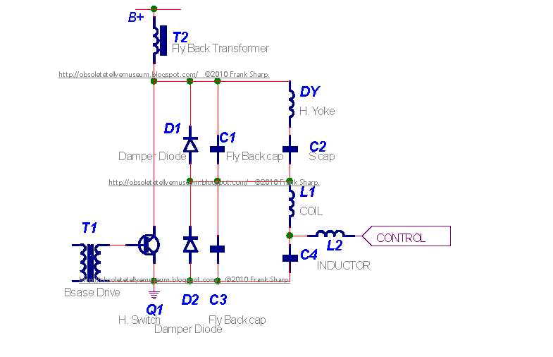
AUTOVOX TVC2608 OMICRON CHASSIS 100 Simplified horizontal / line deflection circuit.

 -----------------------------------------------------------------------------------------------
This AUTOVOX TVC2608 OMICRON CHASSIS 100 Series was featuring a Simplified BU208A transitor horizontal deflection section replacing all Thyristor horizontal timebase based circuits.

 A horizontal deflection circuit makes a sawtooth
current flow through a deflection coil. The current
will have equal amounts of positive and negative
current. The horizontal switch transistor conducts
for the right hand side of the picture. The damper
diode conducts for the left side of the picture.
Current only flows through the fly back capacitor
during retrace time.
For time 1 the transistor is turned on. Current
ramps up in the yoke. The beam is moved from the
center of the picture to the right edge. Energy is
stored on the inductance of the yoke.
E=I2L/2

For time 2 the transistor is turned off. Energy
transfers from the yoke to the flyback capacitor. At
the end of time two all the energy from the yoke is
placed on the flyback capacitor. There is zero
current in the yoke and a large voltage on the
capacitor. The beam is quickly moved from the
right edge back to the middle of the picture.
 During time 3 the energy on the capacitor flows
back into the yoke. The voltage on the flyback
capacitor decreases while the current in the yoke
builds until there is no voltage on the capacitor. By
the end of time 3 the yoke current is at it's
maximum amount but in the negative direction.
The beam is quickly deflected form the center to the
left edge.

Time 4 represents the left hand half of the picture.
Yoke current is negative and ramping down. The
beam moves from the left to the center of the
picture.
The current that flows when the horizontal switch is
closed is approximately:
Ipk ≅ Vcc T / Ldy
Ipk = collector current
T = 1/2 trace time
Ldy = total inductance (yoke + lin coil + size coil)
note:The lin coil inductance varies with current.
______
Tr ≅ 3.14 √ L C
The current that flows during retrace is produced by
the C and L oscillation. The retrace time is 1/2 the
oscillation frequency of the L and C.
I2L /2 ≅ V2C /2 or I2L = V2C As stated earlier the energy in the yoke moves to the
flyback capacitor during time 2.
V= the amount of the flyback pulse that is above the
supply voltage.
 D.C. annualizes is inductors are considered
shores, capacitors are open and generally
semiconductors are removed. The voltage at the
point “B+” is the supply voltage. The collector
voltage of Q1 is also at the supply voltage. The
voltage across C2 is equal to the supply voltage.
When we A.C. annualize this circuit we will find
that the collector of Q1 has a voltage that ranges
from slightly negative to 1000 volts positive. The
average voltage must remain the same as the D.C.
value.
In the A.C. annualizes of the circuit, the
inductance of the yoke (DY) and the inductance of
the flyback transformer are in parallel. The
inductance of T2 is much larger than that if the
DY. This results is a total system inductance of
about 10% to 20% less than that of the DY it’s
self.
The voltage across the Q1 is a half sinusoid pulse during the flyback or retrace period and close to zero at
all other times. It is not possible or safe to observe this point on an oscilloscope without a proper high
frequency high voltage probe. Normally use a 100:1 probe suitable for 2,000V peak. The probe must have
been high frequency calibrated recently.
HORIZONTAL SIZE / E/W AMPLITUDE - CORRECTION CIRCUIT:
There are several different methods of adjusting horizontal size.
 SIZE COIL
Add a variable coil to the yoke current path
causes the total inductance to vary with the coils
setting.
The yoke current is related to supply voltage,
trace time and total inductance. This method
has a limited range!
The horizontal section uses a PWM to set the
horizontal size. One DAC sets the horizontal
size and another DAC sets the pincushion and
trap.
The Raster Centering (D.C. centering) is
controlled by a DAC.
On small monitors the retrace time is fixed. On
large monitors or wide frequency range monitors
two different retrace times are available. The flyback time is set by the micro computer by selecting two
different flyback capacitors. At slow frequencies the longer retrace time is selected.
Different S corrector capacitor values are selected by the micro computer. At the highest frequency the
smallest capacitor is selected.
 SPLIT DIODE MODULATOR
This horizontal circuit consists of two parts. D1, C1, C2 and DY are the components as described above.
D2, C3, C4 and L1 are a second “dummy” horizontal section that does not cause deflection current. By the
D.C. analyzing this circuit the voltage across C2 + C4 must equal the supply voltage (B+). Deflection
current in the DY is related to the supply voltage minus the voltage across C4. For a maximum horizontal
size the control point must be held at ground. This causes the dummy section to not operate and the DY
section will get full supply voltage. If the control point is at 1/3 supply then the DY section will be
operating at 2/3 supply.
Note: The impedance of (D1,C1,C2 and DY) and (D2,C3,C4 and L1) makes a voltage divider. If the
control point is not connected then there is some natural voltage on C4. Most split diode monitors are built
to pull power from the dummy section through L2 to ground. A single power transistor shunts from the
control point to ground. It is true that power can be supplied from some other supply through L2 to rise the voltage on C4. For maximum range a bi-directional power amplifier can drive the control point.
The most exciting feature if the split diode modulator is that the flyback pulse, as seen by the flyback
transformer, is the same size at all horizontal size settings.
HORIZONTAL SWITCH/DAMPER DIODE
On the right hand side of the screen, the H. switch transistor conducts current through the deflection yoke.
This current comes from the S correction capacitors, which have a charge equal to the effective supply
voltage. The damper diode allows current for the left hand side of the screen to flow back through the
deflection yoke to the S capacitors.
FLYBACK CAPACITOR
The flyback capacitor connects the hot side of the yoke to ground. This component determines the size and
length of the flyback pulse. ‘Tuning the flyback capacitor’ is done to match the timing of the flyback pulse
to the video blanking time of the video signal. The peak flyback voltage on the horizontal switch must be
set to less that 80% if the Vces specification. The two conditions of time and voltage can be set by three
variables (supply voltage, retrace capacitor and yoke inductance) .
S CAPACITOR
The S capacitors corrects outside versus center linearity in the horizontal scan. The voltage on the S cap
has a parabola plus the DC horizontal supply. Reducing the value of S cap increases this parabola thus
reducing the size of the outside characters and increasing the size of the center characters.
S Capacitor value: Too low: picture will be squashed towards edges.
Too high: picture will be stretched towards edges.
By simply putting a capacitor in series with each coil, the sawtooth waveform is
modified into a slightly sine-wave shape. This reduces the scanning speed near the
edges where the yoke is more sensitive. Generally the deflection angle of the electron
beam and the yoke current are closely related. The problem is the deflection angle
verses the distance of movement on the CRT screen does not have a linear effect.
BASE DRIVE CURRENT
The base drive resistor determines the amount of
base drive. If the transistor is over driven the Vsat
looks very good, but the current fall time is poor.
If the base current is too small the current fall time is very fast. The problem is that the transistor will have many volts across C-E when closed.
The best condition is found by placing the transistor in the heaviest load condition. Adjust the base resistor for the least power consumption then increase the base drive a small amount. This will slightly over drive the base.
npn transistors,pnp transistors,transistors
Category: NPN Transistor, Transistor
MHz: <1 MHz
Amps: 5A
Volts: 1500V
HIGH VOLTAGE CAPABILITY
JEDEC TO-3 METAL CASE.
DESCRIPTION
The BU208A, BU508A and BU508AFI are
manufactured using Multiepitaxial Mesa
technology for cost-effective high performance
and use a Hollow Emitter structure to enhance
switching speeds.
APPLICATIONS:
* HORIZONTAL DEFLECTION FOR COLOUR TV With 110° or even 90° degree of deflection angle.
ABSOLUTE MAXIMUM RATINGS
Symbol Parameter Value Unit
VCES Collector-Emit ter Voltage (VBE = 0) 1500 V
VCEO Collector-Emit ter Voltage (IB = 0) 700 V
VEBO Emitter-Base Voltage (IC = 0) 10 V
IC Collector Current 8 A
ICM Collector Peak Current (tp < 5 ms) 15 A
TO - 3 TO - 218 ISOWATT218
Ptot Total Dissipation at Tc = 25 oC 150 125 50 W
Tstg Storage Temperature -65 to 175 -65 to 150 -65 to 150 oC
Tj Max. Operating Junction Temperature 175 150 150 °C
 AUTOVOX TVC2608 OMICRON Power Supply CONSTANT-VOLTAGE CONVERTER EMPLOYING THYRISTOR:
A constant voltage converter having a rectifier for rectifying AC power and with a thyristor connected between the rectifier and a filter for selectively passing therethrough a rectified output to an output terminal. There is a wave generator connected to the output of the rectifier for producing a first signal and an intergrator circuit connected to the output of the wave generator for producing an integral output in response to this first signal. In addition there is a detector circuit for detecting a fluctuation of the rectified output power and for producing second signal. A comparison circuit is connected between the intergrator circuit and the detector circuit for producing third signal in accordance with the comparison. A trigger circuit is connected between the comparison circuit and the control gate of the thyristor for supplying a phase control signal to the thyristor to thereby obtain a constant voltage output regardless of the fluctuation of the rectified output.
AUTOVOX TVC2608 OMICRON CHASSIS 100 Simplified horizontal / line deflection circuit.

This AUTOVOX TVC2608 OMICRON CHASSIS 100 Series was featuring a Simplified BU208A transitor horizontal deflection section replacing all Thyristor horizontal timebase based circuits.

 A horizontal deflection circuit makes a sawtooth
current flow through a deflection coil. The current
will have equal amounts of positive and negative
current. The horizontal switch transistor conducts
for the right hand side of the picture. The damper
diode conducts for the left side of the picture.
Current only flows through the fly back capacitor
during retrace time.
For time 1 the transistor is turned on. Current
ramps up in the yoke. The beam is moved from the
center of the picture to the right edge. Energy is
stored on the inductance of the yoke.
E=I2L/2

For time 2 the transistor is turned off. Energy
transfers from the yoke to the flyback capacitor. At
the end of time two all the energy from the yoke is
placed on the flyback capacitor. There is zero
current in the yoke and a large voltage on the
capacitor. The beam is quickly moved from the
right edge back to the middle of the picture.
 During time 3 the energy on the capacitor flows
back into the yoke. The voltage on the flyback
capacitor decreases while the current in the yoke
builds until there is no voltage on the capacitor. By
the end of time 3 the yoke current is at it's
maximum amount but in the negative direction.
The beam is quickly deflected form the center to the
left edge.

Time 4 represents the left hand half of the picture.
Yoke current is negative and ramping down. The
beam moves from the left to the center of the
picture.
The current that flows when the horizontal switch is
closed is approximately:
Ipk ≅ Vcc T / Ldy
Ipk = collector current
T = 1/2 trace time
Ldy = total inductance (yoke + lin coil + size coil)
note:The lin coil inductance varies with current.
______
Tr ≅ 3.14 √ L C
The current that flows during retrace is produced by
the C and L oscillation. The retrace time is 1/2 the
oscillation frequency of the L and C.
I2L /2 ≅ V2C /2 or I2L = V2C As stated earlier the energy in the yoke moves to the
flyback capacitor during time 2.
V= the amount of the flyback pulse that is above the
supply voltage.
 D.C. annualizes is inductors are considered
shores, capacitors are open and generally
semiconductors are removed. The voltage at the
point “B+” is the supply voltage. The collector
voltage of Q1 is also at the supply voltage. The
voltage across C2 is equal to the supply voltage.
When we A.C. annualize this circuit we will find
that the collector of Q1 has a voltage that ranges
from slightly negative to 1000 volts positive. The
average voltage must remain the same as the D.C.
value.
In the A.C. annualizes of the circuit, the
inductance of the yoke (DY) and the inductance of
the flyback transformer are in parallel. The
inductance of T2 is much larger than that if the
DY. This results is a total system inductance of
about 10% to 20% less than that of the DY it’s
self.
The voltage across the Q1 is a half sinusoid pulse during the flyback or retrace period and close to zero at
all other times. It is not possible or safe to observe this point on an oscilloscope without a proper high
frequency high voltage probe. Normally use a 100:1 probe suitable for 2,000V peak. The probe must have
been high frequency calibrated recently.
HORIZONTAL SIZE / E/W AMPLITUDE - CORRECTION CIRCUIT:
There are several different methods of adjusting horizontal size.
 SIZE COIL
Add a variable coil to the yoke current path
causes the total inductance to vary with the coils
setting.
The yoke current is related to supply voltage,
trace time and total inductance. This method
has a limited range!
The horizontal section uses a PWM to set the
horizontal size. One DAC sets the horizontal
size and another DAC sets the pincushion and
trap.
The Raster Centering (D.C. centering) is
controlled by a DAC.
On small monitors the retrace time is fixed. On
large monitors or wide frequency range monitors
two different retrace times are available. The flyback time is set by the micro computer by selecting two
different flyback capacitors. At slow frequencies the longer retrace time is selected.
Different S corrector capacitor values are selected by the micro computer. At the highest frequency the
smallest capacitor is selected.
 SPLIT DIODE MODULATOR
This horizontal circuit consists of two parts. D1, C1, C2 and DY are the components as described above.
D2, C3, C4 and L1 are a second “dummy” horizontal section that does not cause deflection current. By the
D.C. analyzing this circuit the voltage across C2 + C4 must equal the supply voltage (B+). Deflection
current in the DY is related to the supply voltage minus the voltage across C4. For a maximum horizontal
size the control point must be held at ground. This causes the dummy section to not operate and the DY
section will get full supply voltage. If the control point is at 1/3 supply then the DY section will be
operating at 2/3 supply.
Note: The impedance of (D1,C1,C2 and DY) and (D2,C3,C4 and L1) makes a voltage divider. If the
control point is not connected then there is some natural voltage on C4. Most split diode monitors are built
to pull power from the dummy section through L2 to ground. A single power transistor shunts from the
control point to ground. It is true that power can be supplied from some other supply through L2 to rise the voltage on C4. For maximum range a bi-directional power amplifier can drive the control point.
The most exciting feature if the split diode modulator is that the flyback pulse, as seen by the flyback
transformer, is the same size at all horizontal size settings.
HORIZONTAL SWITCH/DAMPER DIODE
On the right hand side of the screen, the H. switch transistor conducts current through the deflection yoke.
This current comes from the S correction capacitors, which have a charge equal to the effective supply
voltage. The damper diode allows current for the left hand side of the screen to flow back through the
deflection yoke to the S capacitors.
FLYBACK CAPACITOR
The flyback capacitor connects the hot side of the yoke to ground. This component determines the size and
length of the flyback pulse. ‘Tuning the flyback capacitor’ is done to match the timing of the flyback pulse
to the video blanking time of the video signal. The peak flyback voltage on the horizontal switch must be
set to less that 80% if the Vces specification. The two conditions of time and voltage can be set by three
variables (supply voltage, retrace capacitor and yoke inductance) .
S CAPACITOR
The S capacitors corrects outside versus center linearity in the horizontal scan. The voltage on the S cap
has a parabola plus the DC horizontal supply. Reducing the value of S cap increases this parabola thus
reducing the size of the outside characters and increasing the size of the center characters.
S Capacitor value: Too low: picture will be squashed towards edges.
Too high: picture will be stretched towards edges.
By simply putting a capacitor in series with each coil, the sawtooth waveform ismodified into a slightly sine-wave shape. This reduces the scanning speed near the
edges where the yoke is more sensitive. Generally the deflection angle of the electron
beam and the yoke current are closely related. The problem is the deflection angle
verses the distance of movement on the CRT screen does not have a linear effect.
BASE DRIVE CURRENT
The base drive resistor determines the amount of
base drive. If the transistor is over driven the Vsat
looks very good, but the current fall time is poor.
If the base current is too small the current fall time is very fast. The problem is that the transistor will have many volts across C-E when closed.
The best condition is found by placing the transistor in the heaviest load condition. Adjust the base resistor for the least power consumption then increase the base drive a small amount. This will slightly over drive the base.
BU208(A)
Silicon NPNnpn transistors,pnp transistors,transistors
Category: NPN Transistor, Transistor
MHz: <1 MHz
Volts: 1500V
HIGH VOLTAGE CAPABILITY
JEDEC TO-3 METAL CASE.
DESCRIPTION
The BU208A, BU508A and BU508AFI are
manufactured using Multiepitaxial Mesa
technology for cost-effective high performance
and use a Hollow Emitter structure to enhance
switching speeds.
APPLICATIONS:
* HORIZONTAL DEFLECTION FOR COLOUR TV With 110° or even 90° degree of deflection angle.
ABSOLUTE MAXIMUM RATINGS
Symbol Parameter Value Unit
VCES Collector-Emit ter Voltage (VBE = 0) 1500 V
VCEO Collector-Emit ter Voltage (IB = 0) 700 V
VEBO Emitter-Base Voltage (IC = 0) 10 V
IC Collector Current 8 A
ICM Collector Peak Current (tp < 5 ms) 15 A
TO - 3 TO - 218 ISOWATT218
Ptot Total Dissipation at Tc = 25 oC 150 125 50 W
Tstg Storage Temperature -65 to 175 -65 to 150 -65 to 150 oC
Tj Max. Operating Junction Temperature 175 150 150 °C
AUTOVOX TVC2608 OMICRON Power Supply CONSTANT-VOLTAGE CONVERTER EMPLOYING THYRISTOR:A constant voltage converter having a rectifier for rectifying AC power and with a thyristor connected between the rectifier and a filter for selectively passing therethrough a rectified output to an output terminal. There is a wave generator connected to the output of the rectifier for producing a first signal and an intergrator circuit connected to the output of the wave generator for producing an integral output in response to this first signal. In addition there is a detector circuit for detecting a fluctuation of the rectified output power and for producing second signal. A comparison circuit is connected between the intergrator circuit and the detector circuit for producing third signal in accordance with the comparison. A trigger circuit is connected between the comparison circuit and the control gate of the thyristor for supplying a phase control signal to the thyristor to thereby obtain a constant voltage output regardless of the fluctuation of the rectified output.
1. A constant voltage converter comprising an input of a power supply means, an output terminal, filter means, rectifier means connected to said input for rectifying a.c. power and for supplying output thereof to said output terminal, thyristor means connected between said rectifier means and said filter means for selectively passing therethrough a rectified output to the output terminal by way of said filter means, saw-tooth wave generator means connected between the output of said rectifier means and at least one integrator circuit means for producing an integral output in response to a saw-tooth wave produced, a first transistor in said saw-tooth wave generator, the input of said integrator circuit means being connected to a collector of said first transistor, detector circuit means c
onnected to said output terminal for detecting a fluctuation of the rectified output power and for producing an output signal, said detector circuit means having a second transistor, pulse generator circuit means connected between said saw-tooth wave generator means and said detector circuit means for producing a trigger pulse to said thyristor through a trigger means, a third transistor in said pulse circuit generator means, the base of said third transistor being connected to the output of said integrator circuit means, the emitter thereof being connected to the emitter of said second transistor in said detector circuit means, and the collector thereof being connected to the gate of the thyristor means so as to supply a phase control signal thereto, thereby obtaining a constant voltage output regardless of the fluctuation of the rectified output.
Description:
This invention relates to constant-voltage converters and more particularly to a constant-voltage converter employing a thyristor.
Conventional con stant-voltage converters of the type employing a thyristor are arranged to phase shift and full-wave-rectify an input a.c. power applied thereto and to maintain the output voltages constant by regulating the firing angle of the thyristor in comparison of the output voltages with the phase-shifted and rectified input a.c. power. When, however, these converters are connected to a common a.c. source having a relatively high internal impedance, the waveform of the phase-shifted and rectified a.c. input power is distorted thereby causing undesired operations of the converters.
It is therefore an object of the present invention to provide a constant-voltage converter which correctly operates notwithstanding the distortion of the input a.c. voltage.
Another object of the invention is to provide a constant-voltage converter which effectively suppress an undesired rush current.
Another object of the invention is to provide a constant-voltage converter having an improved feed-back circuit of a substantially constant loop gain .
In the drawings:
FIG. 1 is a schematic view of a converter according to the present invention;
FIG. 2 is a diagram showing a circuit arrangement of the converter of FIG. 1;
FIG. 3 is a diagram showing various waveforms of signals appearing in the circuit of FIG. 2;
FIG. 4 is a diagram showing various waveforms appearing in the circuit of FIG. 2 when an a.c. power is supplied to the circuit;
FIG. 5 is a diagram showing another circuit arrangement of the converter of FIG. 1;
FIG. 6 is a diagram showing waveforms of signals appearing in the circuit of FIG. 5; and
FIG. 7 is a diagram showing further another circuit arrangement of generator the of FIG. 1.
Referring now to FIG. 1, a cons tant-voltage converter 10 according to the present invention comprises a rectifier 11 having two input terminals 12 and 13 through which an a.c. power is supplied. The rectifier 11 is preferably a full-wave rectifier although a half-wave rectifier may be employed. An output 14 of the rectifier 11 is connected through a line 15 to an anode of a thyristor 16. The thyristor 16 passes therethrough the rectified a.c. power in only one direction from its anode to cathode when triggered by a trigger pulse through its gate. The cathode of the thyristor 16 is connected through a line 17 to an input of a smoothing filter 18. The smoothing filter 18 smoothes the power from the thyristor 16. An output of the smoothing filter 18 is connected through a line 19 to an output terminal 20. The output 14 of the rectifier 11 is also connected through a line 21 to a saw-tooth wave generator 22 which generates a saw-tooth wave signal having the same repetition period as the rectified input a.c. power. An output of the saw-tooth wave generator 22 is connected through a line 23 to one input of a trigger pulse generator 24. The other input of the trigger pulse generator 24 is connected through a line 25 to the line 19. An output of the trigger pulse generator 24 is connected through a line 26 to the gate of the thyristor 16. The trigger pulse generator 24 produces a trigger pulse on its output when the voltage of the saw-tooth wave signal reaches a level which is varied in response to the output voltage on the terminal 20. The trigger pulse generator 24 may be variously arranged and in this case arranged to comprise rectangular generator 27 having one input connected through the line 23 to the saw-tooth wave generator 22 and the other input connected through a line 28 to an output voltage detector 29. The detector 29 produces a reference signal representing the output voltage on the terminal 20. The pulse generator 27 is adapted to produces a rectangular pulse when the saw-tooth wave signal to the one input reaches a level which defined is in accordance with the reference signal. An output of the rectangular pulse generator 27 is connected through a line 30 to an input of a trigger circuit 31. The trigger circuit 31 is adapted to convert the rectangular pulse into a spike pulse. An output of the trigger circuit 31 is connected through the line 26 to the gate of the thyristor 16.
FIG. 2 illustrates a prefe rred circuit arrangement of the converter shown in FIG. 1 which comprises a rectifier 11 of a full-wave rectifier consisting of rectifiers 40, 41, 42 and 43. Inputs of the rectifier are connected to terminals 12 and 13 through which an a.c. power is applied. The output 14 of the rectifier 11 is connected through a line 15 to an anode of a thyristor 16. A cathode of the thyristor 16 is connected through a line 17 to a smoothing filter 18 which includes a capacitor C4 having one terminal connected to the line 17 and the other terminal grounded. The output of the smoothing filter 18 is connected through a line 19 to an output terminal 20.
The saw-tooth wave generator 22 includes a resistor R 1 having one terminal connected to the line 21 and the terminal connected through a junction J 1 to one terminal of a resistor R 2 . The other terminal of the resistor R 2 is grounded. The junction J 1 is connected through a coupling capacitor C 1 to a base of a transistor T 1 of PNP type. An emitter of the transistor T 1 is connected through a resistor R 3 to the line 21. A resistor R 4 is provided between the emitter and the base of the transistor T 1 so as to apply a bias potential to the base. A collector of the transistor T 1 is grounded through a parallel connection of a resistor R 5 and capacitor C 2 . To the emitter is connected a capacitor C 3 which is in turn grounded and passes therethrough only a.c. signals to the ground.
The rectangular pulse generator 27 comprises a transistor T 2 of PNP type having a base connected through a resistor R 6 to the collector of the transistor T 1 . An emitter of the transistor T 2 is connected through a resistor R 7 to the emitter of the transistor T 1 . A collector of the transistor T 2 is grounded through a resistor R 8 and connected through the line 30 to one terminal of a capacitor C 4 of the trigger circuit 31. The other terminal of the capacitor C 4 is connected through a line 26 to the gate of the thyristor 16.
The output voltage detector 29 includes a transistor T 3 of NPN type having an emitter grounded through a zener diode ZD. A collector of the transistor T 3 is connected through a line 28 to the emitter of the transistor T 2 and, on the other hand, connected through a capacitor C 5 to the grounded. A base of the transistor T 3 is connected to a tap of an adjustable resistor R 9 connected through a resistor R 10 and a line 25 to the line 19 and connected, in turn, to the ground through a resistor R 11 .
When, in operation, an a.c. electric power is applied through the input terminals 12 and 13 of the rectif ier 11, a full-wave rectified power as shown in FIG. 3 (a) appears on the output 14. The rectified power is applied through the line 15 to the anode of the thyristor 16. The thyristor 16 passes therethrough the rectified power while its firing angle is regulated by the trigger signal applied to the gate. The rectified power passed through the thyristor 16 is applied through the line 17 to the smoothing filter 18. The smoothing filter smoothes the power by removing the ripple component in the power. The smoothed power appears on the line 19 which is to be supplied to a load through the output terminal 20. The smoothed power on the line 19 is, on the other hand, delivered through the line 25 to the resistor R 10 of the output voltage detector 29. The resistor R 10 constitutes a voltage divider in cooperation with the resistors R 9 and R 11 . The output of the voltage divider is applied through the tap of the resistor R 9 to the base of the transistor T 3 . When the potential of the base of the transistor T 3 exceeds the zener voltage of the zener diode ZD, a base current flows through the transistor T 3 so as to render the transistor T 3 conductive. The potential of the collector of the transistor T 3 then varies in accordance with the voltage of the smoothed output power on the line 19. The potential variation at the collector of the transistor T 3 is then applied through the line 28 to the trigger pulse generator 27 and utilized to regulate the triggering timing of the thyristor 16.
The full-wave rectified power is, on the other hand, applied through the line 21 to the saw-tooth wave generator 22. Since the resistors R 1 and R 2 consistute a voltage divider to reduce the voltage of the full-wave rectified power to a potential at the junction J 1 , a charging current to the capacitor C 1 flows from the emitter to the base of the transistor T 1 whereby the transistor T 1 repeats ON-OFF operation in accordance with the voltage of the rectified power. If the transistor T 1 is conductive when the voltage of the full-wave rectified power is lower than a threshold voltage v 1 as shown in FIG. 3(a), then the potential at the collector of the transistor T 1 is varied as shown in FIG. 3 (b) due to the charge and discharge of the capacitor C 2 . The variation of the potential at the collector of the transistor T 1 is supplied through the line 23 to the resistor R 6 of the trigger pulse generator 27.
As long as the voltage of the smoothed power on the line 19 equals to the rated output voltage, the transistor T 2 is adapted to become conductive when the voltage of the saw-tooth wave signal falls below a threshold value v 3 shown in FIG. 3(b). Therefore, a potential at the collector of the transistor T 2 varies as shown in FIG. 3(c). The potential variation, that is, a pulse signal at the collector of the transistor T 2 is supplied through the line 30 to the capacitor C 4 of the trigger circuit trigger 31. The trigger circuit 31 converts the pulse signal into a spike pulse or a trigger pulse shown in FIG. 3(d) which is then applied through the line 25 to the gate of the thyristor 16. Upon receiving the spike pulse, the thyristor 16 becomes conductive until the voltage of the rectified power on the line 15 falls below the cut-off voltage of the thyristor 16.
When the voltage of the smoothed power on the line 19 exceeds the rated output voltage, the collector current of the transistor T 3 increases with the result that the current flowing through the resistor R 7 increases. The threshold voltage of the transistor T 2 therefore reduces to a voltage v 2 as shown in FIG. 3(b). At this instant, leading edge of the pulse signal delays as shown by dot-and-dash lines in FIG. 3(c), so that each trigger pulse delays as shown by dot-and-dash line in FIG. 3(d). When on the contrary, the voltage of the smoothed signal on the line 19 lowers below the rated output voltage, the collector current of the transistor T 3 decreases whereby the threshold voltage rises to a voltage v 4 in FIG. 3(b). Each leading edge of the signal pulse now leads as shown by dotted line in FIG. 3(d). Being apparent from the above description, the appearance timing of each trigger pulse is regulated in accordance with the voltage of the smoothed power on the line 19 so that the voltage of the output voltage at the terminal 20 is held substantially constant.
Referring now to FIG. 4, start operation of the converte r 10 is discussed hereinbelow in conjunction with FIG. 2. When an a.c. voltage is applied to the input terminals 12 and 13, the capacitor C 3 begins to be charged by the voltage on the line 15, and the capacitor C 5 also begins to be charged through the resistors R 3 and R 7 . It is important that the time constant of power supply circuit constituted by the resistor R 3 and the capacitor C 3 is selected to be much larger than that of the time constant of another power supply circuit constituted by the resistor R 7 and the capacitor C 5 . Thus, the emitter potential of the transistor T 1 is built up more quickly than that of the transistor T 2 . Upon completion of the charging of the capacitor C 3 , the saw-tooth wave generator 22 begins to generate saw-tooth wave signal as shown in FIG. 4(b). Since the capacitor C 5 is, on the other hand, slowly charged, the emitter voltage of the transistor T 2 slowly rises as shown in FIG. 4(c), so that, the threshold voltage of the transistor T 2 gradually rises as shown by a dotted line in FIG. 4 (b). Accordingly, the trigger pulses is produced on the gate of the thyristor 16 as shown in FIG. 4(d), whereby the firing angle of the thyristor 16 is gradually reduced as shown in FIG. 4(a) which illustrates the voltage at the output terminal 14 of the rectifier 11. The output voltage on the output terminal 20 therefore gradually rise up as shown in FIG. 4(e). It is to be understood that since the output voltage of the converter 10 starts to gradually rise up as shown in FIG. 4(e), an undesired rush current is effectively suppressed.
FIG. 5 illustrates another fo rm of the converter 10 which is arranged identically to the circuit arrangement of FIG. 1 except that an integrator 50 is interposed between the output of the saw-tooth wave generator 22 and the input of the trigger pulse generator 27. The integrator 50 includes a resistor R 12 having one terminal connected to the output of the saw-tooth wave generator 22 and the other terminal connected to the input of the rectangular pulse generator 27, and a capacitor C 7 having one terminal connected to the other terminal of the resistor R 12 and the other terminal grounded.
In operation, the saw-tooth wave generator 22 produces on its ouput a saw-tooth wave signal having decreasing exponential wave form portion as shown in FIG. 6 (a), although the saw-tooth wave signal ideally is illustrated in FIG. 3. This saw-tooth wave signal is converted by the integrator 50 into another form of saw-tooth wave having a increasing exponential wave form portion as shown in FIG. 6(b).
It should be noted that the saw-tooth wave signal of FIG. 6(a) has a smaller inclination near 180°. Hence, when the integrator 50 is omitted and the saw-tooth wave signal as shown in FIG. 6(a) is applied to the trigger pulse generator 27, the rate of change of the output voltage of the converter 10 become larger at a firing angle near to 1 80°. On the other hand, it is apparent from FIG. 6(c) that the rate of change the output voltage of the thyristor 16 with respect to the firing angle become large at a firing angle near to 180°. Therefore, the loop gain of the trigger pulse generator 24 increases when the firing angle of the thyristor 16 is near to 180°. It is apparent through a similar discussion that the loop gain of the trigger pulse generator 24 decreases when the firing angle is near to 90°. Such non-uniformity of the loop gain of the trigger pulse generator invites a difficulty of the regulation of the output voltage of the converter. It is to be noted that the saw-tooth wave signal shown in FIG. 6(b) has a large inclination at an angle near 180°. Therefore, when the saw-tooth wave signal of FIG. 6(b) is applied to the trigger pulse generator 24, the loop gain of the trigger pulse generator 24 is held substantially constant, whereby the output voltage of the converter is effectively held constant.
 It is to be understood that the integrator 50 may be substituted for by a miller integrator and a bootstrap integrator. Furthermore, a plurality of integrator may be employed, if desired.
FIG. 7 illustrates another circuit arrangement of the converter according to the present invention, which is arranged identically to the circuit of FIG. 2 except for the trigger circuit 31 and the smoothing circuit 18.
The trigger circuit 31 of FIG. 7 comprises a transformer TR with primary and secondary coils. One terminal of the primary coil is connected to the resistor R 7 of the pulse generator 27. The other terminal of the primary coil is connected to a collector of a transistor T 4 of NPN type. The secondary coil has terminals respectively connected to the gate and cathode of the thyristor 16. An emitter of the transistor T 4 is grounded through a resistor R 13 . A base of the transistor T 4 is grounded through a resistor R 14 and connected through a capacitor C 8 to the collector of the transistor T 2 of the pulse generator 27.
The smoothing filter 18 of FIG. 7 comprises a choke coil CH connected to the lines 17 and 19, and to capacitors C 9 and C 10 which are in turn grounded. The circuit of FIG. 7 operates in the same manner as the circuit of FIG. 2.
Obviously many modifications and variations of the present invention are possible in the light of the above teachings. It is therefore to be understood that within the scope of the appended claims the invention may be practiced otherwise than as specifically described.
Conventional con
stant-voltage converters of the type employing a thyristor are arranged to phase shift and full-wave-rectify an input a.c. power applied thereto and to maintain the output voltages constant by regulating the firing angle of the thyristor in comparison of the output voltages with the phase-shifted and rectified input a.c. power. When, however, these converters are connected to a common a.c. source having a relatively high internal impedance, the waveform of the phase-shifted and rectified a.c. input power is distorted thereby causing undesired operations of the converters.It is therefore an object of the present invention to provide a constant-voltage converter which correctly operates notwithstanding the distortion of the input a.c. voltage.
Another object of the invention is to provide a constant-voltage converter which effectively suppress an undesired rush current.
Another object of the invention is to provide a constant-voltage converter having an improved feed-back circuit of a substantially constant loop gain .
In the drawings:
FIG. 1 is a schematic view of a converter according to the present invention;
FIG. 2 is a diagram showing a circuit arrangement of the converter of FIG. 1;
FIG. 3 is a diagram showing various waveforms of signals appearing in the circuit of FIG. 2;
FIG. 4 is a diagram showing various waveforms appearing in the circuit of FIG. 2 when an a.c. power is supplied to the circuit;
FIG. 5 is a diagram showing another circuit arrangement of the converter of FIG. 1;
FIG. 6 is a diagram showing waveforms of signals appearing in the circuit of FIG. 5; and
FIG. 7 is a diagram showing further another circuit arrangement of generator the of FIG. 1.
Referring now to FIG. 1, a cons
tant-voltage converter 10 according to the present invention comprises a rectifier 11 having two input terminals 12 and 13 through which an a.c. power is supplied. The rectifier 11 is preferably a full-wave rectifier although a half-wave rectifier may be employed. An output 14 of the rectifier 11 is connected through a line 15 to an anode of a thyristor 16. The thyristor 16 passes therethrough the rectified a.c. power in only one direction from its anode to cathode when triggered by a trigger pulse through its gate. The cathode of the thyristor 16 is connected through a line 17 to an input of a smoothing filter 18. The smoothing filter 18 smoothes the power from the thyristor 16. An output of the smoothing filter 18 is connected through a line 19 to an output terminal 20. The output 14 of the rectifier 11 is also connected through a line 21 to a saw-tooth wave generator 22 which generates a saw-tooth wave signal having the same repetition period as the rectified input a.c. power. An output of the saw-tooth wave generator 22 is connected through a line 23 to one input of a trigger pulse generator 24. The other input of the trigger pulse generator 24 is connected through a line 25 to the line 19. An output of the trigger pulse generator 24 is connected through a line 26 to the gate of the thyristor 16. The trigger pulse generator 24 produces a trigger pulse on its output when the voltage of the saw-tooth wave signal reaches a level which is varied in response to the output voltage on the terminal 20. The trigger pulse generator 24 may be variously arranged and in this case arranged to comprise rectangular generator 27 having one input connected through the line 23 to the saw-tooth wave generator 22 and the other input connected through a line 28 to an output voltage detector 29. The detector 29 produces a reference signal representing the output voltage on the terminal 20. The pulse generator 27 is adapted to produces a rectangular pulse when the saw-tooth wave signal to the one input reaches a level which defined is in accordance with the reference signal. An output of the rectangular pulse generator 27 is connected through a line 30 to an input of a trigger circuit 31. The trigger circuit 31 is adapted to convert the rectangular pulse into a spike pulse. An output of the trigger circuit 31 is connected through the line 26 to the gate of the thyristor 16.FIG. 2 illustrates a prefe
rred circuit arrangement of the converter shown in FIG. 1 which comprises a rectifier 11 of a full-wave rectifier consisting of rectifiers 40, 41, 42 and 43. Inputs of the rectifier are connected to terminals 12 and 13 through which an a.c. power is applied. The output 14 of the rectifier 11 is connected through a line 15 to an anode of a thyristor 16. A cathode of the thyristor 16 is connected through a line 17 to a smoothing filter 18 which includes a capacitor C4 having one terminal connected to the line 17 and the other terminal grounded. The output of the smoothing filter 18 is connected through a line 19 to an output terminal 20.The saw-tooth wave generator 22 includes a resistor R 1 having one terminal connected to the line 21 and the terminal connected through a junction J 1 to one terminal of a resistor R 2 . The other terminal of the resistor R 2 is grounded. The junction J 1 is connected through a coupling capacitor C 1 to a base of a transistor T 1 of PNP type. An emitter of the transistor T 1 is connected through a resistor R 3 to the line 21. A resistor R 4 is provided between the emitter and the base of the transistor T 1 so as to apply a bias potential to the base. A collector of the transistor T 1 is grounded through a parallel connection of a resistor R 5 and capacitor C 2 . To the emitter is connected a capacitor C 3 which is in turn grounded and passes therethrough only a.c. signals to the ground.
The rectangular pulse generator 27 comprises a transistor T 2 of PNP type having a base connected through a resistor R 6 to the collector of the transistor T 1 . A
n emitter of the transistor T 2 is connected through a resistor R 7 to the emitter of the transistor T 1 . A collector of the transistor T 2 is grounded through a resistor R 8 and connected through the line 30 to one terminal of a capacitor C 4 of the trigger circuit 31. The other terminal of the capacitor C 4 is connected through a line 26 to the gate of the thyristor 16.The output voltage detector 29 includes a transistor T 3 of NPN type having an emitter grounded through a zener diode ZD. A collector of the transistor T 3 is connected through a line 28 to the emitter of the transistor T 2 and, on the other hand, connected through a capacitor C 5 to the grounded. A base of the transistor T 3 is connected to a tap of an adjustable resistor R 9 connected through a resistor R 10 and a line 25 to the line 19 and connected, in turn, to the ground through a resistor R 11 .
When, in operation, an a.c. electric power is applied through the input terminals 12 and 13 of the rectif
ier 11, a full-wave rectified power as shown in FIG. 3 (a) appears on the output 14. The rectified power is applied through the line 15 to the anode of the thyristor 16. The thyristor 16 passes therethrough the rectified power while its firing angle is regulated by the trigger signal applied to the gate. The rectified power passed through the thyristor 16 is applied through the line 17 to the smoothing filter 18. The smoothing filter smoothes the power by removing the ripple component in the power. The smoothed power appears on the line 19 which is to be supplied to a load through the output terminal 20. The smoothed power on the line 19 is, on the other hand, delivered through the line 25 to the resistor R 10 of the output voltage detector 29. The resistor R 10 constitutes a voltage divider in cooperation with the resistors R 9 and R 11 . The output of the voltage divider is applied through the tap of the resistor R 9 to the base of the transistor T 3 . When the potential of the base of the transistor T 3 exceeds the zener voltage of the zener diode ZD, a base current flows through the transistor T 3 so as to render the transistor T 3 conductive. The potential of the collector of the transistor T 3 then varies in accordance with the voltage of the smoothed output power on the line 19. The potential variation at the collector of the transistor T 3 is then applied through the line 28 to the trigger pulse generator 27 and utilized to regulate the triggering timing of the thyristor 16.The full-wave rectified power is, on the other hand, applied through the line 21 to the saw-tooth wave generator 22. Since the resistors R 1 and R 2 consistute a voltage divider to reduce the voltage of the full-wave rectified power to a potential at the junction J 1 , a charg
ing current to the capacitor C 1 flows from the emitter to the base of the transistor T 1 whereby the transistor T 1 repeats ON-OFF operation in accordance with the voltage of the rectified power. If the transistor T 1 is conductive when the voltage of the full-wave rectified power is lower than a threshold voltage v 1 as shown in FIG. 3(a), then the potential at the collector of the transistor T 1 is varied as shown in FIG. 3 (b) due to the charge and discharge of the capacitor C 2 . The variation of the potential at the collector of the transistor T 1 is supplied through the line 23 to the resistor R 6 of the trigger pulse generator 27.As long as the voltage of the smoothed power on the line 19 equals to the rated output voltage, the transistor T 2 is adapted to become conductive when the voltage of the saw-tooth wave signal falls below a threshold value v 3 shown in FIG. 3(b). Therefore, a potential at the collector of the transistor T 2 varies as shown in FIG. 3(c). The potential variation, that is, a pulse signal at the collector of the transistor T 2 is supplied through the line 30 to the capacitor C 4 of the trigger circuit trigger 31. The trigger circuit 31 converts the pulse signal into a spike pulse or a trigger pulse shown in FIG. 3(d) which is then applied through the line 25 to the gate of the thyristor 16. Upon receiving the spike pulse, the thyristor 16 becomes conductive until the voltage of the rectified power on the line 15 falls below the cut-off voltage of the thyristor 16.
When the voltage of the smoothed power on the line 19 exceeds the rated output voltage, the collector current of the transistor T 3 increases with the result that the current flowing through the resistor R 7 increases. The threshold voltage of the transistor T 2 therefore reduces to a voltage v 2 as shown in FIG. 3(b). At this instant, leading edge of the pulse signal delays as shown by dot-and-dash lines in FIG. 3(c), so that each trigger pulse delays as shown by dot-and-dash line in FIG. 3(d). When on the contrary, the voltage of the smoothed signal on the line 19 lowers below the rated output voltage, the collector current of the transistor T 3 decreases whereby the threshold voltage rises to a voltage v 4 in FIG. 3(b). Each leading edge of the signal pulse now leads as shown by dotted line in FIG. 3(d). Being apparent from the above description, the appearance timing of each trigger pulse is regulated in accordance with the voltage of the smoothed power on the line 19 so that the voltage of the output voltage at the terminal 20 is held substantially constant.
Referring now to FIG. 4, start operation of the converte
r 10 is discussed hereinbelow in conjunction with FIG. 2. When an a.c. voltage is applied to the input terminals 12 and 13, the capacitor C 3 begins to be charged by the voltage on the line 15, and the capacitor C 5 also begins to be charged through the resistors R 3 and R 7 . It is important that the time constant of power supply circuit constituted by the resistor R 3 and the capacitor C 3 is selected to be much larger than that of the time constant of another power supply circuit constituted by the resistor R 7 and the capacitor C 5 . Thus, the emitter potential of the transistor T 1 is built up more quickly than that of the transistor T 2 . Upon completion of the charging of the capacitor C 3 , the saw-tooth wave generator 22 begins to generate saw-tooth wave signal as shown in FIG. 4(b). Since the capacitor C 5 is, on the other hand, slowly charged, the emitter voltage of the transistor T 2 slowly rises as shown in FIG. 4(c), so that, the threshold voltage of the transistor T 2 gradually rises as shown by a dotted line in FIG. 4 (b). Accordingly, the trigger pulses is produced on the gate of the thyristor 16 as shown in FIG. 4(d), whereby the firing angle of the thyristor 16 is gradually reduced as shown in FIG. 4(a) which illustrates the voltage at the output terminal 14 of the rectifier 11. The output voltage on the output terminal 20 therefore gradually rise up as shown in FIG. 4(e). It is to be understood that since the output voltage of the converter 10 starts to gradually rise up as shown in FIG. 4(e), an undesired rush current is effectively suppressed.FIG. 5 illustrates another fo
rm of the converter 10 which is arranged identically to the circuit arrangement of FIG. 1 except that an integrator 50 is interposed between the output of the saw-tooth wave generator 22 and the input of the trigger pulse generator 27. The integrator 50 includes a resistor R 12 having one terminal connected to the output of the saw-tooth wave generator 22 and the other terminal connected to the input of the rectangular pulse generator 27, and a capacitor C 7 having one terminal connected to the other terminal of the resistor R 12 and the other terminal grounded.In operation, the saw-tooth wave generator 22 produces on its ouput a saw-tooth wave signal having decreasing exponential wave form portion as shown in FIG. 6 (a), although the saw-tooth wave signal ideally is illustrated in FIG. 3. This saw-tooth wave signal is converted by the integrator 50 into another form of saw-tooth wave having a increasing exponential wave form portion as shown in FIG. 6(b).
It should be noted that the saw-tooth wave signal of FIG. 6(a) has a smaller inclination near 180°. Hence, when the integrator 50 is omitted and the saw-tooth wave signal as shown in FIG. 6(a) is applied to the trigger pulse generator 27, the rate of change of the output voltage of the converter 10 become larger at a firing angle near to 1
 80°. On the other hand, it is apparent from FIG. 6(c) that the rate of change the output voltage of the thyristor 16 with respect to the firing angle become large at a firing angle near to 180°. Therefore, the loop gain of the trigger pulse generator 24 increases when the firing angle of the thyristor 16 is near to 180°. It is apparent through a similar discussion that the loop gain of the trigger pulse generator 24 decreases when the firing angle is near to 90°. Such non-uniformity of the loop gain of the trigger pulse generator invites a difficulty of the regulation of the output voltage of the converter. It is to be noted that the saw-tooth wave signal shown in FIG. 6(b) has a large inclination at an angle near 180°. Therefore, when the saw-tooth wave signal of FIG. 6(b) is applied to the trigger pulse generator 24, the loop gain of the trigger pulse generator 24 is held substantially constant, whereby the output voltage of the converter is effectively held constant.
FIG. 7 illustrates another circuit arrangement of the converter according to the present invention, which is arranged identically to the circuit of FIG. 2 except for the trigger circuit 31 and the smoothing circuit 18.
The trigger circuit 31 of FIG. 7 comprises a transformer TR with primary and secondary coils. One terminal of the primary coil is connected to the resistor R 7 of the pulse generator 27. The other terminal of the primary coil is connected to a collector of a transistor T 4 of NPN type. The secondary coil has terminals respectively co
nnected to the gate and cathode of the thyristor 16. An emitter of the transistor T 4 is grounded through a resistor R 13 . A base of the transistor T 4 is grounded through a resistor R 14 and connected through a capacitor C 8 to the collector of the transistor T 2 of the pulse generator 27.The smoothing filter 18 of FIG. 7 comprises a choke coil CH connected to the lines 17 and 19, and to capacitors C 9 and C 10 which are in turn grounded. The circuit of FIG. 7 operates in the same manner as the circuit of FIG. 2.
Obviously many modifications and variations of the present invention are possible in the light of the above teachings. It is therefore to be understood that within the scope of the appended claims the invention may be practiced otherwise than as specifically described.


IF VIDEO DEMOD + AMPL + SOUND IF unit (Motorola TBA120C) (Motorola CA270BE) VIF STAGE
- CHROMINANCE unit (PHILIPS TBA570 + TBA540 + TAA630S)
- LUMINANCE + SYNCHRONIZATION unit (TBA920)
- Color difference amplifier + Luminance amplifier stage unit
- Line deflection output unit. (Texas Instruments BU208A)
- Frame deflection output unit. ( 2 x Motorola BD142-4 )
- E/W Correction output unit. (RCA BD182)
The Luminance and the chrominance are amplified and performed in separate way until the CRT MATRIX (CRT DE MATRIXING)
THE Philips TBA SERIES
The TBA series of i.c.s developed by Philips for use in TV receivers comprises the TBA500Q, TBA510Q, TBA520Q, TBA530Q, TBA540Q, TBA550Q, TBA560Q, TBA750Q and TBA990Q, the Q signifying that the lead out pins are in zig-zag form as illustrated in other posts here at Obsolete Technology Tellye !
The operations the various i.c.s in this series perform are as follows:
TBA500Q: Luminance Combination. Luminance amplifier for colour receivers incorporating luminance delay line matching stages, gated black level clamp and a d.c. contrast control which maintains a constant black level over its range of operation. A c.r.t. beam limiter facility is incorporated, first reducing the picture contrast and then the brightness. Line and field flyback blanking can also be applied.
TBA510Q: Chrominance Combination. Chrominance amplifier for colour receivers incorporating a gain controlled stage, a d.c. control for saturation which can be ganged to the receiver's contrast control, burst gating and blanking, a colour killer, and burst output and PAL delay line driver stages.
TBA520Q: Chrominance Demodulator. Incorporates U and V synchronous demodulators, G-Y matrix and PAL V switch. This type will be superseded by
the TBA990Q (development of which was nearing completion in 1972) listed later.
TBA530Q: RGB Matrix. Luminance and colour difference signal matrix incorporating preamplifiers.
TBA540Q: Reference Combination. Decoder reference oscillator (with external crystal) and a.p.c. loop. Also provides a.c.c., colour killer and ident outputs. TBA550Q: Video signal processor for colour or monochrome receivers. This i.c. is the successor to the TAA700. It is very similar electrically to the TAA700. TBA560Q: Luminance and Chrominance Combination. Provides luminance and chrominance signal channels for a colour receiver. Although not equivalent to the TBA500Q and TBA510Q it performs similar functions to those i.c.s.
TBA750Q: Intercarrier Sound Channel. Incorporates five stage intercarrier sound limiter/amplifier plus quadrature detector and audio preamplifier. External
TBA990Q: Chrominance Demodulator. Incorporates U and V synchronous demodulators, G -Y matrix and PAL V switch. This is at the time in the final stages of development and was been available from March 1972 onwards. As I have given information previously on the TBA550Q and TBA750Q we may concentrate in this and the concluding post in the series on the colour receiver i.c.s. such as multistandard sets or bistandard color decoders here at Obsolete Technology Tellye !
Fig. 1 shows in block diagram form their application for luminance and chrominance signal processing. We will look first at the TBA520Q an
 d TBA530Q which are in use for example in the Philips G8 single standard colour chassis.
TBA530Q RGB Matrix Preamplifier:
The internal circuitry of this i.c. is shown in Fig. 2 while Fig. 3 shows the immediate external connections as used in the Philips G8 chassis. The chip layout is designed to ensure tight thermal coupling between all transistors to minimise thermal drift between channels and each channel has an identical layout to the others to ensure equal frequency response characteristics. The colour -difference signals are fed in at pins 2, 3 and 4 and the luminance input is at pin 5. Trl and Tr2 form the matrix in each channel, driving the differential amplifiers Tr3, Tr4, Tr5. The operating conditions are set by Tr5 and Tr7, using an external current -determining resistor connected to pin 7. Pin 6 is the chassis connection and pin 8 the 12V supply line connection (maximum voltage permitted 13.2V, approximate current consumption 30mA). External load resistors are connected to pins 1, 14 and 11 from a 200V line and the outputs are taken from pins 16, 13 and 10. The output pins are internally connected to the load resistor pins via Tr6
 which provides a zener-type junction giving a level shift appropriate
for driving the bases of the external output transistors directly.
External l0kpF capacitors are required between the output and load
resistor pins to bypass these zener junctions at h.f. Feedback from the
external output stages is fed in at pins 15, 12 and 9. A common supply
line should be used for this and any other i.c.s in the series used in
the decoder, to ensure that any changes in the black level caused by
variations in the supply voltage occur in a predictable way : the
stability of the supply should be not worse than ±3% due to operational
variations to limit changes in picture black level during receiver
operation. To reduce the possibility of patterning on the picture due to
radiation of the harmonics of the demodulation
which provides a zener-type junction giving a level shift appropriate
for driving the bases of the external output transistors directly.
External l0kpF capacitors are required between the output and load
resistor pins to bypass these zener junctions at h.f. Feedback from the
external output stages is fed in at pins 15, 12 and 9. A common supply
line should be used for this and any other i.c.s in the series used in
the decoder, to ensure that any changes in the black level caused by
variations in the supply voltage occur in a predictable way : the
stability of the supply should be not worse than ±3% due to operational
variations to limit changes in picture black level during receiver
operation. To reduce the possibility of patterning on the picture due to
radiation of the harmonics of the demodulation process the leads carrying the drive signals to the tube should be kept
as short as possible : resistors (typically 1.51J) connected in series
with the leads and mounted close to the collectors of the out- put
transistors provide useful additional filtering of these harmonics.
process the leads carrying the drive signals to the tube should be kept
as short as possible : resistors (typically 1.51J) connected in series
with the leads and mounted close to the collectors of the out- put
transistors provide useful additional filtering of these harmonics. TBA520Q Chrominance Demodulator:
 In addition to U and V balanced synchronous detectors this i.c. incorporates a PAL switch which inverts on alternate lines the V reference signal fed to the V synchronous detector. The PAL switch is controlled by an integrated flip-flop circuit which is driven by line frequency pulses and is under the control of an ident input to synchronise the V switching. Outputs from the U and V demodulators are matrixed within the i.c. to obtain the G-Y signal so that all three colour difference signals are available at pins 4, 5 and 7. The internal circuit of this i.c. is shown in Fig. 4 while Fig. 5 shows the immediate external circuitry as used in the Philips G8 chassis. The separated U and ±V chrominance signals from the PAL delay line/matrix circuit are fed in at pins 9 and 13 respectively. The U and V reference signals, in phase quadrature, are fed in at pins 8 and 2. Taking the U channel first we see that the U chrominance signal is fed to Tr18 base. This transistor with Tr19 forms a differential pair which drives the emitters of the transistors-Tr4, Try, Tr6 and Tr7-which comprise the U synchronous demodulator. The U reference signal is fed to Tr12 base, this transistor with Tr13 forming a further differential pair which drive the bases of the synchronous demodulator transistors. The B -Y signal is developed across R3 and appears at output pin 7. A similar arrangement is followed in the V channel except that here the V reference signal fed in at pin 2 to the base of Tr22 is routed to the V synchronous demodulator (Tr8-Tr11) via the PAL switch Tr14-Tr17. This switch is controlled by the integrated flip-flop (bistable) Tr24 and Tr25 (with diodes DI and D2). The bases of the transistors in the flip-flop circuit are driven by negative goin
 g
line frequency pulses fed in at pins 14 and 15. As a result half line
frequency antiphase squarewaves are developed across R13 and R14 and fed
to the PAL switch via R57 and R58. The ident signal is fed into the
base of Tr32 at pin 1. A positive -going input to pin 1 drives Tr32 on
so that the base of Tr24 is shorted and the flip-flop rendered inactive
until the positive input is removed. In the Philips circuit a 4V peak
-to -peak 7.8kHz sinewave ident signal is fed in at pin 1 to synchronise
the flip-flop. The squarewave signal is externally available at pin 3
from the emitter -follower Tr39 which requires an external load
resistor. The R-Y signal developed across R9 is fed via R10 to output
pin 4. The G-Y signal appears at the output of the matrix network R4, R5
and R6 and is fed via R7 to pin 5. The d.c. voltages applied to pins 11
and 12 establish the correct G -Y and R-Y signal levels relative to the
B -Y signal. Pin 10 is internally connected and no external connection
should be made to this pin. The U and V reference carrier inputs should
be about IV p -p, via a d.c. blocking capacitor in each feed. These
inputs must not be less than 0-5V. The flip-flop starts when the voltage
at pin 1 is reduced The amplitudes of the pulses fed in at pins 14 and
15 below 0.4V : it should not be allowed to exceed -5V. to drive the
flip-flop should be between 2.5 and 5V p-p.
g
line frequency pulses fed in at pins 14 and 15. As a result half line
frequency antiphase squarewaves are developed across R13 and R14 and fed
to the PAL switch via R57 and R58. The ident signal is fed into the
base of Tr32 at pin 1. A positive -going input to pin 1 drives Tr32 on
so that the base of Tr24 is shorted and the flip-flop rendered inactive
until the positive input is removed. In the Philips circuit a 4V peak
-to -peak 7.8kHz sinewave ident signal is fed in at pin 1 to synchronise
the flip-flop. The squarewave signal is externally available at pin 3
from the emitter -follower Tr39 which requires an external load
resistor. The R-Y signal developed across R9 is fed via R10 to output
pin 4. The G-Y signal appears at the output of the matrix network R4, R5
and R6 and is fed via R7 to pin 5. The d.c. voltages applied to pins 11
and 12 establish the correct G -Y and R-Y signal levels relative to the
B -Y signal. Pin 10 is internally connected and no external connection
should be made to this pin. The U and V reference carrier inputs should
be about IV p -p, via a d.c. blocking capacitor in each feed. These
inputs must not be less than 0-5V. The flip-flop starts when the voltage
at pin 1 is reduced The amplitudes of the pulses fed in at pins 14 and
15 below 0.4V : it should not be allowed to exceed -5V. to drive the
flip-flop should be between 2.5 and 5V p-p. For a colou bar signal a U input of approximately 360mV is required at pin 9 and a V input of approximately 500mV is required at pin 13. The supply is fed in at pin 6 and this also sets the d.c. level of the B-Y output signal. The maximum voltage allowed at this pin is 13.2V. In early versions of the Philips G8 chassis a TAA630 i.c. was used in place of the TBA520Q.
Philips TBA SERIES SINCE the last part in this series Philips have released details of a PAL -D decoder developed in their laboratories in which most of the circuitry has been integrated into four i.c.s a TBA560Q which undertakes the luminance and chrominance signal processing, a TBA540Q which provides the reference signal channel, a TBA990Q which provides synchronous demodulation of the colour -difference signals, G -Y signal matrixing and PAL V switching, and a TBA530Q which matrixes the colour -difference signals and the luminance signal to obtain the R, G and B signals which after amplification by single -transistor output stages drive the cathodes of the shadowmask tube.
The TBA540Q and TBA560Q and also the TBA500Q and TBA510Q which provide an alternative luminance and chrominance signal processing arrangement will be covered this time.
The internal circuits of the TBA530Q and TBA520Q (predecessor to the TBA990Q which shows how fast things are moving at present) were shown in Part 6 in order to give an idea of the type of circuitry used in these linear colour receiver i.c.s. The internal circuitry is not however of great importance to the user or service engineer: all we need to know about a particular i.c. are the functions it performs, the inputs and outputs it requires and provides and the external connections necessary. The i.c.s we shall deal with in this instalment are highly complex internally the TBA560Q for example contains some 67 integrated transistor elements alone. This time therefore we shall just show the immediate external circuitry in conjunction with a block diagram to indicate the functions performed within the i.c.
TBA540Q Reference Signal Channel:

A block diagram with external connections for this i.c. is shown in Fig. 1. In addition to providing the reference signal required for synchronous demodulation of the colour difference signals this i.c. incorporates automatic phase and amplitude control of the reference oscillator and a half line frequency synchronous demodulator which compares the phases and amplitudes of the burst ripple and the square waveform from the PAL V switch circuit in order to generate a.c.c., colour killer and ident outputs. The use of a synchronous demodulator for these functions provides a high standard of noise immunity in the decoder. The internal reference oscillator operates in conjunction with an external 4.43MHz crystal connected between pins 1 and 15. The nominal load capacitance of the crystal is 20pF. The reference oscillator output, in correct phase for feeding to the V signal synchronous demodulator, is taken from pin 4 at a nominal amplitude of 1.5V peak -to -peak. This is a low -impedance output and no d.c. load to earth is required here. The bifilar inductor Ll provides the antiphase signal necessary for push-pull reference signal drive to the burst detector circuit, the antiphase input being at pin 6. The U subcarrier is obtained from the junction of a 900 phase shift network (R1, C1) connected across Ll. The oscillator is controlled by the output at pin 2. This pin is fed internally with a sinewave derived from the reference signal and controlled in amplitude by the internal reactance control circuit. The phase of the feedback from pin 2 to the crystal via C2 is such that the value of C2 is effectively increased. Pin 2 is held internally at a very low impedance. Thus the tuning of the crystal is automatically controlled by the amplitude of the feedback waveform and its influence on the effective value of C2. The burst signal is fed in at pin 5. A burst waveform amplitude of 1V peak -to -peak is required (the minimum threshold is 0.7V) and this is a.c. coupled. The a.p.c. loop phase detector (burst detector) loads and filter (R2, C4, C5 and C6) are connected to pins 13 and 14. A synchronously -generated a.c.c. potential is produced at pin 9. The voltage at this pin is set by R3 to 4V with zero burst input. The synchronous demodu- lator producing this output is fed with the burst signal and the PAL half line frequency squarewave which is a.c. coupled at pin 8 at 2.5V peak -to -peak. If the phase of the squarewave is correct the potential at pin 9 will fall and normal a.c.c. action will commence. If the phase of the squarewave is incorrect the voltage at pin 9 will rise, providing the ident action as this rise will make the PAL switch miss a count thereby correcting its phase. A colour -killer output is provided at pin 7 from an internal switching transistor. If the ident conditions are incorrect this transistor is saturated and the output at pin 7 is about 250mV. When the ident conditions are correct (voltage at pin 9 below 2.5V) the transistor is cut off providing a positive -going turn -on bias at pin 7. The network between pins 10 and 12 provides filtering and a.c.c. level (R3) setting. The control connected to pin 11 is set so that in conjunction with the rest of the decoder circuitry the level of the burst signal at pin 5 under a.c.c. control is correct. The positive d.c. supply required is applied to pin 3 and the chassis connection is pin 16.
TBA560Q Chroma-Luminance IC:

A block diagram with external connections for this i.c. is shown in Fig. 2. The i.c. incorporates the circuits required to process the luminance and chrominance signals, providing a luminance output for the RGB matrix and a chrominance output for the PAL delay line circuit.
The luminance input is a.c. coupled from the luminance delay line terminating resistor at pin 3. This pin also requires a d.c. bias current which is obtained via the 22kI resistor shown. The brightness control is connected to pin 6: variation from OV to 1 2V at this pin gives a variation in the black level of the luminance output at pin 5 of from OV to 3V, which is a greater range than is needed in practice. The contrast control is connected to pin 2 and the potential applied here controls the gain of both the luminance and the chrominance channels so that the two signals track together correctly. Picture tube beam current limiting can be applied at either pin 6 or pin 2 (by taking the earthy side of one of the controls to a beam limiter network). To maintain correct picture black level it is preferable to apply the beam limiting facility to reduce the contrast. A positive going pulse timed to coincide with the back porch period is fed in at pin 10 to provide burst gating and to operate the black -level clamp in the luminance channel: the black -level clamp requires a charge storage capacitor which is connected to pin 4. The luminance output is obtained from an internal emitter follower at pin 5, an external load resistor of not less than 2kS2 being required here. The output has a nominal black level of 1.6V and 1V black -to -white amplitude. The chrominance signal is applied in push-pull to pins 1 and 15. A.c.c. is applied at pin 14, a negative going potential giving a 26dB control range starting at 1V and giving maximum gain reduction at 200mV. The saturation control is connected to pin 13 and the colour -killer potential is also applied to this pin : the chrominance channel is muted when the voltage at this pin falls below IV. The chrominance output, at an amplitude of about 2V peak -to -peak, is obtained at pin 9: an external network is required which provides d.c. negative feedback in the chrominance channel via pin 12. The burst output, at about 1V peak -to -peak, is obtained at pin 7. A network connected to this pin also provides d.c. feedback to the chrominance input transformer (connected between pins 1 and 15) to give good d.c. stability. Line and field blanking pulses are fed in at pin 8 to the luminance and chrominance channels : these negative -going pulses should not exceed -5V in amplitude. The d.c. supply is applied to pin 11 and pin 16 is the chassis connection.
TBA500Q Luminance IC:
A block diagram with external connections for this i.c. is shown in Fig. 3. This i.c. provides a colour receiver luminance channel incorporating luminance delay -line matching stages, a black -level clamp and a d.c. contrast control which maintains a constant black level over its range of operation. A beam current limiting facility which first reduces picture ,contrast and then picture brightness is provided and line and field flyback blanking can be applied. A video input signal of 2V peak -to -peak with negative -going sync pulses is required at pin 2, a.c. coupled. A clamp potential obtained from pin 13 via a smoothing circuit is fed to pin 2 to regulate the black level of the signal at pin 2 to about 10-4V. The smoothing network for the black -level control potential should have a time -constant which is less than the time constant of the video signal coupling network. The 3V peak -to -peak composite video output with positive -going sync pulses obtained at pin 3 from an emitter -follower can be used as a source of chroma signal: in Fig. 3 it is used as a source of sync pulses for the black -level clamp, fed in at pin 15. This pin requires positive -going sync pulses of 2V amplitude or greater for sync -cancelling the black -level clamp. The other input to the clamp consists of negative going back porch pulses fed in at pin 1 to operate th
 e
clamp. The timing of these pulses is not critical provided the pulse
does not encroach on the sync pulse period and that it dwells for at
least Zus on any part of the back porch-clamp pulse overlap into the
picture line period is unimportant. A low-pass filter capacitor for the
clamp is connected at pin 14 to prevent the operation of the clamp being
affected by the bursts or h.f. noise. The contrast control is connected
to pin 5 and is linked to the saturation control so that the two track
together. A variation of from 2 to 4V at pin 5 gives a control range of
at least 40dB, the relationship between the video at pin 4 and the
potential at pin 5 being linear. An output to drive the luminance delay
line is provided at pin 4. This is a low -impedance source and a
luminance delay line with a characteristic impedance of 1-2.7161 can be
used. The delayed luminance signal is fed back into the i.c. at pin 8.
Line and field flyback banking pulses and the brightness control are
also connected to this pin. The gain of the luminance channel is
determined by the value of the resistor connected to pin 9. The
luminance output is taken from an emitter -follower at pin 10, an
external load resistor being required. The voltage output range
available is from 0.7V to 5-5V. The potential of the black level of the
output signal is normally set to 1.5V by appropriate setting of the
potential at pin 8. A luminance signal output amplitude of 2.8V black to
white at maximum contrast is produced : superimposed on this is the
blanking waveform which remains of constant amplitude independently of
the contrast and brightness control settings. A beam current limiting
input is provided at pin 6. A rising positive potential at this pin will
start to reduce the contrast at about 2V. Further increase in the
voltage at this pin will continue to reduce the contrast until a
threshold is reached, determined by the potential applied to pin 7, when
the d.c. level of the video signal is reduced giving reduction in
picture brightness. The d.c. supply is connected to pin 12 and pin 16 is
the chassis connection.
e
clamp. The timing of these pulses is not critical provided the pulse
does not encroach on the sync pulse period and that it dwells for at
least Zus on any part of the back porch-clamp pulse overlap into the
picture line period is unimportant. A low-pass filter capacitor for the
clamp is connected at pin 14 to prevent the operation of the clamp being
affected by the bursts or h.f. noise. The contrast control is connected
to pin 5 and is linked to the saturation control so that the two track
together. A variation of from 2 to 4V at pin 5 gives a control range of
at least 40dB, the relationship between the video at pin 4 and the
potential at pin 5 being linear. An output to drive the luminance delay
line is provided at pin 4. This is a low -impedance source and a
luminance delay line with a characteristic impedance of 1-2.7161 can be
used. The delayed luminance signal is fed back into the i.c. at pin 8.
Line and field flyback banking pulses and the brightness control are
also connected to this pin. The gain of the luminance channel is
determined by the value of the resistor connected to pin 9. The
luminance output is taken from an emitter -follower at pin 10, an
external load resistor being required. The voltage output range
available is from 0.7V to 5-5V. The potential of the black level of the
output signal is normally set to 1.5V by appropriate setting of the
potential at pin 8. A luminance signal output amplitude of 2.8V black to
white at maximum contrast is produced : superimposed on this is the
blanking waveform which remains of constant amplitude independently of
the contrast and brightness control settings. A beam current limiting
input is provided at pin 6. A rising positive potential at this pin will
start to reduce the contrast at about 2V. Further increase in the
voltage at this pin will continue to reduce the contrast until a
threshold is reached, determined by the potential applied to pin 7, when
the d.c. level of the video signal is reduced giving reduction in
picture brightness. The d.c. supply is connected to pin 12 and pin 16 is
the chassis connection.TBA510Q Chrominance IC:

A block diagram with external connections for this i.c. is shown in Fig. 4. It provides a colour receiver chrominance signal processing channel with a variable gain a.c.c. chroma amplifier circuit, d.c. control of chroma saturation which can be ganged to the opera- tion of the contrast control, chroma blanking and burst gating, a burst output stage, colour -killer circuit and PAL delay line driver stage. The chroma signal is a.c. coupled to pin 4, the a.c.c. control potential being applied at pin 2. The non - signal side of the differential amplifier used for the a.c.c. system is taken to pin 3 where a decoupling capacitor should be connected. A resistor can be connected between pins 2 and 3 to reduce the control sensitivity of the a.c.c. system to any desired level. The saturation control is connected to pin 15, the d.c. control voltage range required here being 1.5-4-5V. For chrominance blanking a negative -going line flyback pulse of amplitude not greater than 5V is fed in at pin 14. A series network is connected to pin 6 to decouple the emitter of one of the amplifying stages in the i.c.: the value of the resistor in this network influences the gain of both the burst and the chroma channels in the i.c. The chrominance signal outputs are obtained at pin 8 (collector) to drive the chroma delay line and pin 9 (emitter) to feed the chrominance signal matrix (undelayed signal). A resistive path to earth is essen- tial at pin 9. The colour -killer turn -on bias is applied to pin 5 : colour is "on" at 2.3V, "off" at 1.9V. Chroma signal suppression when killed is greater than 50dB. The burst signal output is at pin 11 (collector) or 12 (emitter). If a low -impedance output is required pin 11 is connected direct to the 12V supply rail and the output is taken from pin 12. An external load of 2kn connected to chassis is required here. The burst gating pulse is fed in at pin 13, a negative -going pulse of not greater than 5V amplitude being required. Pins 7 and 10 are connected to an internal screen whose purpose is to prevent unwanted burst and chroma outputs : the pins must be linked together and taken via a direct path to earth. Pin 1 is the d.c.
supply pin and pin 16 the chassis connection.
A TBA510 as example is used in the Grundig 1500/3010 series and also the YR 1972 Grundig colour chassis (5010 / 5050 series) introduced in the70's. Grundig continue in these models to favour colour -difference tube drive. The 5010 series uses a TBA510 together with a TAA630 colour demodulator i.c. in the chrominance section and a TBA970 luminance i.c. which drives a single BF458 luminance output transistor operated from a 280V rail. As this series has been appearing more and more i.c.s have come to be used in television receivers, both monochrome and colour, and more and more i.c.s designed for television set use have been announced. Some of these have been mentioned in recent argumentations here in this Web Museum. There seems little doubt that a major increase in the use of integrated circuits in television receivers is about to occur in the future. Fully integrated i.f. and vision detector sections are already in use (PHILIPS K9-K11) and this is the likely area, together with the decoder in colour sets, in which integration will most rapidly spread. Elsewhere integrated line and field oscillators using circuits without inductors have been developed and a field output stage in integrated form is now feasible. Line output stages consisting of hybrid i.c. and thick film circuits (PHILIPS K12) have been built and there is a programme of work directed to the integration of the r.f. tuner, using digital frequency synthesisers to provide local oscillator action controlled by signals from a remote point.
We seem to have reached the position where the only part of the set which does not attract the i.c. manufacturers is the picture tube itself !
TBA920 line oscillator combination
 DESCRIPTION
The line oscillator combination TBA920 is a monolithic
integrated circuit intended for the horizontal deflection of the black and white
and colour TV sets
picture tube.
FEATURES:
SYNC-PULSE SEPARATION
OPTIONAL NOISE INVERSION
GENERATION OF A LINE FREQUENCY VOL-
TAGE BY MEANS OF AN OSCILLATOR
PHASE COMPARISON BETWEEN SYNC-
PULSE AND THE OSCILLATOR WAVEFORM
PHASE COMPARISON BETWEEN THE OS-
CILLATOR WAVEFORM AND THE MIDDLE OF
THE LINE FLY-BACK PULSE
AUTOMATIC SWITCHING OF THE VARIABLE
TRANSCONDUCTANCE AND THE VARIABLE
TIME CONSTANT TO ACHIEVE NOISE SUP-
PRESSION AND, BY SWITCHING OFF, POS-
SIBILITY OF TAPE-VIDEO-REGISTERED RE-
PRODUCTION
SHAPING AND AMPLIFICATION OF THE OS-
CILLATOR WAVEFORM TO OBTAIN PULSES
FOR THE CONTROL OF DRIVING STAGES IN
HORIZONTAL, DEFLECTION CIRCUITS
USING EITHER TRANSISTORS OR THYRISTORS,
BU208(A)
Silicon NPN
npn transistors,pnp transistors,transistors
Category: NPN Transistor, Transistor
MHz: <1 MHz
Amps: 5A
Volts: 1500V
HIGH VOLTAGE CAPABILITY
JEDEC TO-3 METAL CASE.
DESCRIPTION
The BU208A, BU508A and BU508AFI are
manufactured using Multiepitaxial Mesa
technology for cost-effective high performance
and use a Hollow Emitter structure to enhance
switching speeds.
APPLICATIONS:
* HORIZONTAL DEFLECTION FOR COLOUR TV With 110° or even 90° degree of deflection angle.
ABSOLUTE MAXIMUM RATINGS
Symbol Parameter Value Unit
VCES Collector-Emit ter Voltage (VBE = 0) 1500 V
VCEO Collector-Emit ter Voltage (IB = 0) 700 V
VEBO Emitter-Base Voltage (IC = 0) 10 V
IC Collector Current 8 A
ICM Collector Peak Current (tp < 5 ms) 15 A
TO - 3 TO - 218 ISOWATT218
Ptot Total Dissipation at Tc = 25 oC 150 125 50 W
Tstg Storage Temperature -65 to 175 -65 to 150 -65 to 150 oC
Tj Max. Operating Junction Temperature 175 150 150 °C
A vertical deflection circuit for use in a television receiver, comprising a control circuit for stabilizing the width of a pulse either in a vertical oscillator circuit or between a vertical oscillator circuit and vertical output circuit to thereby stabilize the width of a pulse component included in the vertical deflection output signal.
TDA1170 vertical deflection FRAME DEFLECTION INTEGRATED CIRCUIT
GENERAL DESCRIPTION f The TDA1170 and TDA1270 are monolithic integrated
circuits designed for use in TV vertical deflection systems. They are manufactured using
the Fairchild Planar* process.
Both devices are supplied in the 12-pin plastic power package with the heat sink fins bent
for insertion into the printed circuit board.
The TDA1170 is designed primarily for large and small screen black and white TV
receivers and industrial TV monitors. The TDA1270 is designed primarily for driving
complementary vertical deflection output stages in color TV receivers and industrial
monitors.
APPLICATION INFORMATION (TDA1170)
The vertical oscillator is directly synchronized by the sync pulses (positive or negative); therefore its free
running frequency must be lower than the sync frequency. The use of current feedback causes the yoke
current to be independent of yoke resistance variations due to thermal effects, Therefore no thermistor is
required in series with the yoke. The flyback generator applies a voltage, about twice the supply voltage, to
the yoke. This produces a short flyback time together with a high useful power to dissipated power
ratio.
1. A transformerless output vertical deflection circuit, comprising a vertical oscillator circuit for generating a vertical pulse train in response to vertical synchronizing pulses applied thereto, a sawtooth signal generator for generating a series of sawtooth signals, each cycle of said sawtooth signal including a pulse component, a vertical output circuit coupled to said sawtooth generator for amplifying said sawtooth signal including said pulse component and loading a vertical deflection coil, and stabilizing means connected between said vertical oscillator and said sawtooth signal generator for varying the width of the pulse component which is to be fed to said vertical output circuit in response to the average level of DC output voltage fed from the vertical output circuit. 2. A transformerless output vertical deflection circuit claimed in claim 1, wherein said stabilizing means comprises a control circuit means for receiving a series of pulses from the vertical oscillator and a feedback signal from the vertical output circuit and for varying the width of the pulse which is to be fed to the vertical output circuit in response to a DC control signal proportional to the width of the pulse component included in the vertical output signal and smoothing circuit means connected between said vertical output circuit and said stabalizing means for smoothing said feedback signal. 3. A transformerless output vertical deflection circuit claimed in claim 2, wherein said control circuit comprises a charging capacitor which is parallel to a transistor, said transistor being switched on in response to pulses fed from the vertical oscillator wherein said capacitor is charged by the voltage fed from said smoothing circuit, and discharged in response to conduction of the transistor, a differential amplifier circuit which receives the voltage on said capacitor and a fixed voltage, and a gating circuit for producing a pulse which has a width equal to the difference between the width of the pulse fed from the vertical oscillator circuit and the width of pulse fed from the differential amplifier circuit. 4. A transformerless output vertical deflection circuit claimed in claim 2, wherein said control circuit comprises a capacitor which is charged by a fixed power source and is discharged by means of a switching transistor operated by the pulses fed from the vertical oscillator circuit and a differential amplifier circuit receiving the voltage on the capacitor and the output of said smoothing circuit. 5. A transformable output vertical deflection circuit comprising a vertical oscillator for generating a vertical pulse train in response to vertical synchronizing pulses applied thereto, a sawtooth signal generator for generating a series of sawtooth signals each cycle of said sawtooth signal including a pulse component, a vertical output circuit for amplifying said sawtooth signal including said pulse component and loading a vertical deflection coil, and pulse stabilizing means coupled between the vertical oscillator circuit a
nd the sawtooth signal generator, said stabilizing means comprising a capacitor which is charged by a fixed power source and discharged by means of a discharging means operated in response to the vertical pulse fed from the vertical oscillator, a circuit means for generating a train of output pulses each starting at the time when the voltage appearing on the capacitor exceeds a predetermined value and terminating in synchronism with termination of the pulse fed from the vertical oscillator, and gating means for generating pulses having a width equal to the difference between the width of the pulse fed from the vertical oscillator and the width of the output pulse of the circuit means. 6. A transformerless output vertical deflection circuit, comprising a vertical oscillator circuit for generating a vertical pulse train in response to vertical synchronizing pulses applied thereto, a sawtooth signal generator for generating a series of sawtooth signals, each cycle of said sawtooth signal including a pulse component, a vertical output circuit coupled to said sawtooth generator for amplifying said sawtooth signal including said pulse component and loading a vertical deflection coil, and stabilizing means, comprising a control circuit connected between said vertical output circuit and said vertical oscillator circuit for varying the width of each pulse produced by the vertical oscillator circuit in response to a DC control signal having a value corresponding to the width of the pulse component applied to the vertical deflection coil of the vertical output circuit for controlling the pulse width of the output of said vertical oscillator circuit and thereby the pulse width of said pulse component.
Description:
BACKGROUND OF THE INVENTION
The present invention relates to a vertical deflection circuit for use in a television receiver and, more particularly, to a vertical deflection circuit of a type wherein no vertical output transformer is employed. This type of vertical deflection circuit with no output transformer is generally referred to as an OTL (Output Transformerless) type vertical deflection circuit.
It is known that variation of the pulse width of the flyback pulse produced in a vertical output stage of the vertical deflection circuit is the cause in the raster on the television picture tube, of a white bar, flicker, jitter, line crowding and/or other raster disorders. In addition thereto, in the vertical deflection output circuit where the output stage is composed of a single-ended push-pull amplifier having a vertical output transistor, an excessive load is often imposed on the output transistor and, in an extreme case, the output transistor is destroyed.
AUTOVOX TVC2608 OMICRON Amplifier
suitable for use as a color kinescope driver:A color kinescope matrix amplifier has a first input coupled through a capacitor to a source of color difference signals. Another input is coupled to a source of luminance signals. The matrix amplifier includes a cascode output stage direct current coupled to a cathode of a kinescope. A portion of a direct voltage developed at the cascode output amplifier is coupled to one input of a comparator circuit. The other input of the comparator circuit is coupled to a temperature compensated direct voltage reference source. The comparator is rendered operative during horizontal retrace intervals to provide a current to either charge or discharge the input capacitor in accordance with the difference between the voltage at the output of the cascode output amplifier and the reference voltage to compensate for voltage variations at the output of the cascode amplifier due to power supply variations and the like. To compensate for droop caused by the discharge of the input capacitor during the scanning interval, one input of a differential amplifier is included between the input capacitor and the input of the cascode output stage. Negative signal feedback is provided from the output stage to the other input of the differential amplifier via a capacitor arranged to be charged during the horizontal retrace interval. The two capacitors discharge at substantially the same rates during the scanning interval. By virtue of the common mode operation of the differential amplifier droop effects are minimized.
1. In a tel
evision receiver including an image reproducing device, a source of chrominance signals, a source of luminance signals and a source of horizontal blanking pulses, said horizontal blanking pulses occurring during the time interval during which said image reproducing device is horizontally retraced, the apparatus comprising:
amplifying means for combining said chrominance signals and said luminance signals, said amplifying means including first and second input terminals and an output terminal, said output terminal being direct current coupled to said image reproducing device, said second input terminal being direct current coupled to said source of said luminance signals;
first capacitive means for coupling said chrominance signals to said first input terminal;
comparator means having first and second input terminals for comparing voltages applied thereto, said comparator means being normally inoperative;
a relatively low level stabilized reference voltage source coupled to said first input terminal of said comparator means;
means coupled to said second input terminal of said comparator means for providing a direct voltage proportional to the direct voltage developed at said output terminal;
means for selectively rendering said comparator operative in response to said horizontal blanking pulses; and
current converting means coupled to said comparator and to said first capacitive means for charging and discharging said capacitive means to a direct voltage level in relation to the difference in voltage between said first and second input terminals of said comparator means so as to counteract the changes of the voltage developed at said output terminal.
2. The apparatus recited in claim 1 wherein said amplifying means includes:
a differential amplifier having first and second input terminals and an output terminal, said first input terminal being coupled to sai d first input terminal of said amplifying means, said output terminal of said differential amplifier being coupled to said output terminal of said amplifying means;
d first input terminal of said amplifying means, said output terminal of said differential amplifier being coupled to said output terminal of said amplifying means;
second capacitive means coupled to said second input terminal of said differential amplifier; and
means for selectively charging said second capacitive means during said horizontal retrace interval, said first and second capacitive means being selected to have substantially equal discharging rates during the time intervals between said horizontal retrace intervals.
3. The apparatus recited in claim 2 wherein said second capacitive means is coupled between said output terminal of said ampl ifying means and said second input terminal of said differential amplifier. 4. The apparatus recited in claim 3 wherein said amplifying means includes a cascode amplifier coupled between the output of said differential amplifier and said output terminal of said amplifying means. 5. The apparatus recited in claim 3 wherein said amplifying means includes first and second transistors, the emitter of said first transistor being direct current coupled to the collector of said second transistor, the base of said first transistor being coupled to said first input terminal of said amplifying means, the base of said second transistor being coupled to said second input terminal of said amplifying means, the emitter of said first transist
 or being coupled to said first input terminal of said differential amplifier. 6. The apparatus recited in claim 3 wherein said means for selectively charging said second capacitive means includes means for clamping the second input terminal of said differential amplifier to a predetermined voltage during said horizontal retrace interval. 7. The apparatus recited in claim 3 wherein means are provided for adjusting the portion of the voltage developed at said output terminal of said amplifying means which is coupled to said second capacitive means. 8. The apparatus recited in claim 1 wherein said means coupled to said second input terminal of said comparator means for providing a direct voltage proportional to the direct voltage developed at said output terminal of said amplifying means includes means for adjusting the voltage coupled to said second input terminal of said comparator means. 9. The apparatus recited in claim 1 wherein said comparator means includes:
 ifying means and said second input terminal of said differential amplifier. 4. The apparatus recited in claim 3 wherein said amplifying means includes a cascode amplifier coupled between the output of said differential amplifier and said output terminal of said amplifying means. 5. The apparatus recited in claim 3 wherein said amplifying means includes first and second transistors, the emitter of said first transistor being direct current coupled to the collector of said second transistor, the base of said first transistor being coupled to said first input terminal of said amplifying means, the base of said second transistor being coupled to said second input terminal of said amplifying means, the emitter of said first transistor being coupled to said first input terminal of said differential amplifier. 6. The apparatus recited in claim 3 wherein said means for selectively charging said second capacitive means includes means for clamping the second input terminal of said differential amplifier to a predetermined voltage during said horizontal retrace interval. 7. The apparatus recited in claim 3 wherein means are provided for adjusting the portion of the voltage developed at said output terminal of said amplifying means which is coupled to said second capacitive means. 8. The apparatus recited in claim 1 wherein said means coupled to said second input terminal of said comparator means for providing a direct voltage proportional to the direct voltage developed at said output terminal of said amplifying means includes means for adjusting the voltage coupled to said second input terminal of said comparator means. 9. The apparatus recited in claim 1 wherein said comparator means includes:
a differential amplifier having two input terminals and two output terminals, one of said input terminals being coupled to said reference voltage source, the other of said input terminals being coupled to said output terminal of said amplifier means; and
a current mirror circuit having an input and an output, one of said output terminals of said differential amplifier being coupled to said input terminal of said current mirror circuit, the other of said output terminals of said differential amplifier being coupled to the output of said current mirror circuit and to said first capacitor means.
10. The apparatus recited in claim 1 wherein said voltage reference source is temperature compensated. 11. In a television receiver including a color kinescope leaving a plurality of electron beam forming apparatus, a source of luminance signals, a source of a plurality of color difference signals, and a source of horizontal blanking pulses, said horizontal blanking pulses corresponding to the time interval during which said electron beams are horizontally retraced, the apparatus comprising:
a plurality of amplifiers, each of said amplifiers including
amplifying means for com bining one of said plurality of color difference signals with said luminance signals, said amplifying means including first and second input terminals and an output terminal, said output terminal being direct current coupled to a respective one of said plurality of electron beam forming apparatus, said second input terminal being direct current coupled to said source of said luminance signals, capacitive means for coupling said one of said plurality of color difference signals to said first input terminal,
bining one of said plurality of color difference signals with said luminance signals, said amplifying means including first and second input terminals and an output terminal, said output terminal being direct current coupled to a respective one of said plurality of electron beam forming apparatus, said second input terminal being direct current coupled to said source of said luminance signals, capacitive means for coupling said one of said plurality of color difference signals to said first input terminal,
comparator means having first and second input terminals for comparing voltages applied thereto, said comparator means being normally inoperative,
means coupled to said second input terminal of said comparator means for providing a direct voltage proportional to the direct voltage developed at said output terminal,
means for selectively rendering said comparator operative in response to said horizontal blanking pulses, and
current converting means coupled to said comparator and to said capacitive means for charging and discharging said capacitive means to a direct voltage level in relation to the difference in voltage between said first and second input terminals of said comparator means so as to counteract the changes of the voltage developed at said output terminal; and a relatively low level stabilized reference
voltage source coupled to said first input terminals of each of said plurality of comparator means.
Description:
The present invention is directed to the field of amplifiers and is particularly directed to the field of amplifier arrangements utilized to drive color image reproducing devices such as kinescopes.
The electron guns of a color kinescope are typically driven by separate amplifier stages. Variations of the operating conditions of an amplifier stage, such as variations of the stage's supply voltage, tend to produce variations in the brightness of a reproduced image. Furthermore, because each of the stages tends to operate at different power dissipation levels the operating conditions of the stages vary with respect to each other and hence color imbalances may occur.
Athough supply voltage regulators and high level clamping circuits have been employed in conjunction with kinescope amplifier stages to inhibit the aformentioned problems, it is desirable to provide kinescope driver amplifier arrangements which maintain their operating point stability with variations in operating conditions such as power supply variations without the need of supply voltage regulators or high level clamping circuits.
gh supply voltage regulators and high level clamping circuits have been employed in conjunction with kinescope amplifier stages to inhibit the aformentioned problems, it is desirable to provide kinescope driver amplifier arrangements which maintain their operating point stability with variations in operating conditions such as power supply variations without the need of supply voltage regulators or high level clamping circuits.
Furthermore, it is desirable, because of the trend toward miniaturization in electronic art, that at least a portion of the kinescope amplifier driver should be able to be constructed in integrated circuit form.
It is also desirable to provide kinescope driver amplifier arrangements which include independent controls for adjusting the DC level and the AC amplitude of the signals coupled to the kinescope. This is particularly desirable where "precision-in-line" kinescopes or the like, in which the electron guns have common control electrodes, are employed since, in these types of kinescopes, it is difficult to independently adjust the operating conditions associated with the respective guns because of the commonality of control electrodes.
Furthermore, it is desirable that a kinescope driver amplifier which is to be utilized with a precision-in-line type of kinescope provide a relatively wide bandwidth without the requirement of high frequency peaking coils. Peaking coils tend to be bulky. In addition, undesirable voltages may be developed across a peaking coil due to the large magnetic fields which may be produced by the yokes associated with a precision-in-line kinescope. These undesirable voltages may produce disconcerting brightness and/or hue changes.
In accordance with the present invention, one input terminal of amplifying means is coupled to a source of chrominance signals through capacitive means. A second input of the amplifying means is direct current coupled to a source of luminance signals. The output terminal of the amplifying means is direct current coupled to a color image reproducing device such as a precision-in-line kinescope of the like. The amplifying means includes means for combining the luminance and chrominance signals to provide the image reproducing device with color signals. The amplifying means also includes comparator means for comparing the voltage developed at the output terminal to a reference voltage to generate a current to control the charging of the capacitive means in a manner so as to counter-act the changes of the voltage developed at the output due, for example, to changes in the power supply voltage. The comparator means is arranged to be normally inoperative and is selectively rendered operative during the horizontal retrace interval.
input terminal of amplifying means is coupled to a source of chrominance signals through capacitive means. A second input of the amplifying means is direct current coupled to a source of luminance signals. The output terminal of the amplifying means is direct current coupled to a color image reproducing device such as a precision-in-line kinescope of the like. The amplifying means includes means for combining the luminance and chrominance signals to provide the image reproducing device with color signals. The amplifying means also includes comparator means for comparing the voltage developed at the output terminal to a reference voltage to generate a current to control the charging of the capacitive means in a manner so as to counter-act the changes of the voltage developed at the output due, for example, to changes in the power supply voltage. The comparator means is arranged to be normally inoperative and is selectively rendered operative during the horizontal retrace interval.
In accordance with another aspect of the present invention, the amplifying means includes a differential amplifier having first and second input terminals and an output terminal. The output terminal of the differential amplifier is coupled to the output terminal of the amplifying means. The first input terminal of the differential amplifier is coupled to the input terminal of the amplifying means. The second input terminal of the differential amplifying means is coupled to a second capacitive means. Means are provided for selectively charging the second capacitive means during the horizontal retrace interval. The first and second capacitive means are selected to have substantially equal discharging rates so as to compensate for any decrease in the DC content (i.e., droop) at the output terminal of the amplifying means during the scanning interval.
In accordance with still another feature of the present invention, the second capacitive means is coupled to the output terminal of the amplifying means in a manner so as to allow adjustment of the AC gain of the amplifying means. The DC conditions of the output of the amplifying means may be controlled by controlling the portion of the voltage developed at the output terminal coupled to the comparator means.
with still another feature of the present invention, the second capacitive means is coupled to the output terminal of the amplifying means in a manner so as to allow adjustment of the AC gain of the amplifying means. The DC conditions of the output of the amplifying means may be controlled by controlling the portion of the voltage developed at the output terminal coupled to the comparator means.
The present invention may best be understood by reference to the following detailed description and accompanying drawing which shows, partially in block diagram form and partially in schematic form, the general arrangement of a color television receiver employing a kinescope driver amplifier arrangement constructed in accordance with the present invention .
The color television receiver includes a video signal processing unit 141 responsive to radio frequency (RF) signals, received by an antenna, for receiving in a known manner, a composite video signal comprising chrominance, luminance, sound and synchronizing signal components.
The output of video processing unit 141 is coupled to a chrominance channel 142 including a chrominance processing unit 143 and a color demodulator 144. Chrominance processing unit 143 separates chrominance signals from the composite video signal. Color demodulator 144 derives signals of the appropriate polarity representing, for example, R-Y, G-Y and B-Y color difference signal information from the chrominance signals. The TAA630 integrated circuit or similar circuit is suitable for use as color demodulator 144.
n from the chrominance signals. The TAA630 integrated circuit or similar circuit is suitable for use as color demodulator 144.
The output of video processing unit 141 is also coupled to a luminance channel 145 including a luminance processing unit 146 which amplifies and processes luminance components of the composite signal to form an output signal of the appropriate polarity representing luminance, Y, information. A brightness control unit 147 to control the DC content of luminance signal Y and a contrast control unit 148 to control the amplitude of luminance signal Y are coupled to processing unit 146.
The composite video signal is also coupled to a sync separator 149 which, in turn, is coupled to a horizontal deflection unit 151 and a vertical deflection unit 152. Horizontal deflection unit 151 is also coupled to a high voltage unit 154 which generates operating voltages for kinescope 153. Outputs from horizontal deflection unit 151 and vertical deflection unit 152 are coupled to luminance processing unit 146 to inhibit or blank luminance signal Y during the horizontal and vertical retrace intervals. Similarly, an output from horizontal deflection unit 151 may be coupled to chroma processing unit 143 or color demodulator 144 to inhibit the color difference signals during the horizontal retrace interval. Furthermore, first and second signals including positive going pulses, the pulses of each signal being coincident with the horizontal retrace or blanking interval, are coupled to matrix unit 100 to control its operation, as will appear below, via conductors 159 and 167, respectively.
ocessing unit 146 to inhibit or blank luminance signal Y during the horizontal and vertical retrace intervals. Similarly, an output from horizontal deflection unit 151 may be coupled to chroma processing unit 143 or color demodulator 144 to inhibit the color difference signals during the horizontal retrace interval. Furthermore, first and second signals including positive going pulses, the pulses of each signal being coincident with the horizontal retrace or blanking interval, are coupled to matrix unit 100 to control its operation, as will appear below, via conductors 159 and 167, respectively.
The R-Y output signal and luminance signal Y are coupled to a matrix unit 100 where they are combined to form a color signal representing red (R) information. Similarly, the B-Y and G-Y color difference signals are respectively coupled to matrix-driver units 150 and 157, similar to the combination of matrix unit 100 and kinescope driver 199, where they are matrixed with luminance signal Y to produce color signals representing blue (B) and green (G) information. Since the matrix units for the various color difference signals are similar, only matrix unit 100 will be described in detail.
Matrix unit 100, enclosed within dotted line 160, is suitable for construction as an integrated circuit. The R-Y color difference signal is coupled through a capacitor 110 to the base of an NPN transistor 101 which is arranged as a common collector amplifier for color difference signals. Transistor 101, NPN transistor 102, resistors 178 and 184 form a summing circuit 161 for the color difference signal and luminance signal Y, the latter being direct current coupled to the base of transistor 102. The combined output of circuit 161, taken at the collector of transistor 102, is coupled to the base of an NPN transistor 105. Transistor 105 and an NPN transistor 106 form a differential amplifier 162 to which bias current is supplied from a current source including a suitably biased transistor 182. The output of differential amplifier 162, taken at the collector of transistor 105, is coupled through a level shifter, shown as the series connection of a zener diode 163, and a diode 165 to a kinescope 199. Bias current is provided for zener diode 163 and diode 165 through a resistor 183, which serves as the load resistor of transistor 105, and resistors 176 and 177.
rranged as a common collector amplifier for color difference signals. Transistor 101, NPN transistor 102, resistors 178 and 184 form a summing circuit 161 for the color difference signal and luminance signal Y, the latter being direct current coupled to the base of transistor 102. The combined output of circuit 161, taken at the collector of transistor 102, is coupled to the base of an NPN transistor 105. Transistor 105 and an NPN transistor 106 form a differential amplifier 162 to which bias current is supplied from a current source including a suitably biased transistor 182. The output of differential amplifier 162, taken at the collector of transistor 105, is coupled through a level shifter, shown as the series connection of a zener diode 163, and a diode 165 to a kinescope 199. Bias current is provided for zener diode 163 and diode 165 through a resistor 183, which serves as the load resistor of transistor 105, and resistors 176 and 177.
Kinescope driver 199 comprises a cascode amplifier 164 including NPN transistors 120 and 119. The output of matrix unit 100 is coupled to the base of transistor 119 while a positive supply voltage (e.g. +12 volts) is coupled to the base of transistor 120. The output of kinescope driver 199, taken at the collector of transistor 120 is direct current coupled through a resistor 179 to the red (R) cathode of kinescope 153. The collector of transistor 120 is coupled to a source of supply voltage B+ through a load resistor 165. Supply voltage B+ is a relatively high voltage, typically, in the order of 200 to 300 vdc.
The collector of transistor 120 is also coupled to a series combination of a resistor 166 and a black level setting potentiometer 167, the latter being returned to ground. A direct voltage proportional to that at the collector of transistor 120 is developed at the wiper arm of potentiometer 167 and is coupled to one input of a voltage comparator circuit 168. Comparator 168 comprises NPN transistors 103 and 104 coupled as a differential amplifier. A second input of comparator 168, at the base of transistor 103, is coupled to a temperature compensated voltage reference (TCVR) unit 169. Voltage reference unit 169, which may, for example, be similar to that employed in the CA3085 integrated circuit manufactured by RCA Corporation, supplies a regulated reference voltage of approximately 1.6 vdc.
e wiper arm of potentiometer 167 and is coupled to one input of a voltage comparator circuit 168. Comparator 168 comprises NPN transistors 103 and 104 coupled as a differential amplifier. A second input of comparator 168, at the base of transistor 103, is coupled to a temperature compensated voltage reference (TCVR) unit 169. Voltage reference unit 169, which may, for example, be similar to that employed in the CA3085 integrated circuit manufactured by RCA Corporation, supplies a regulated reference voltage of approximately 1.6 vdc.
Voltage reference unit 169 is also coupled to the matrix portions of units 150 and 157 via conductor 155 so that a common reference voltage is coupled to the respective comparators of units 100, 150 and 157. It is noted that matrix unit 100 and the matrix portions of units 150 and 153 may be constructed as a single integrated circuit.
A current source including an NPN transistor 170 is coupled to the jointly connected emitters of transistors 103 and 104. The first horizontal blanking pulse signal generated by horizontal deflection unit 151 is coupled to the base of transistor 170 via conductor 159.
The output of differential amplifier 168 provided at the collector of NPN transistor 103 is converted to a bidirectional current by means of a current mirror circuit 180 comprising a diode-connected PNP transistor 172 and a PNP transistor 173. The collector of transistor 173 is coupled to the collector of transistor 104 and to the base of transistor 101.
The junction of resistors 166 and 167 is coupled to a signal feedback circuit comprising a series connection of a potentiometer 174 and a resistor 175. Feedback voltage developed at the wiper arm of potentiometer 174 is coupled through a capacitor 120 to the base of transistor 106 (i.e., one input of differential amplifier 162). The base of transistor 106 is returned to ground through resistor 181 and the collector-emitter junction of a transistor 108. The base of transistor 108 is coupled to horizontal deflection unit 151 to receive the first horizontal blanking pulse signal via conductor 159. An NPN transistor 107, the emitter of which is coupled to the base of transistor 106, is arranged together with resistor 181 and the collector-emitter junction of transistor 108 as an emitter follower. The base of transistor 107 is coupled to horizontal deflection unit 151 to receive the second horizontal blanking pulse signal via conductor 167. It is noted that this signal may also be generated within the IC device.
Kinescope 153 may be a precision-in-line kinescope such as the RCA type 15VADTCO1. As is described in U.S. Pat. No. 3,817,397, issued May 21, 1974, there is no provision for separate adjustment of red, green and blue gun screen and grid potentials and only the cathodes of the three guns of such a kinescope are available for separate adjustment of the cut off point of the guns. As will become apparent in the following description, matrix unit 100 and kinescope driver 199 are particularly suited to a kinescope of the precision-in-line type but it should be appreciated that they may be utilized for other types of kinescopes such as delta-gun, shadow mask or other slotted mask types.
In operation, the signal supplied to the base of transistor 107 during the scanning interval by horizontal deflection unit 151 is of sufficiently low amplitude (e.g., less than +4vdc) in relationship to the voltage at its emitter (controlled by the charge on capacitor 120 as will be explained) that it is non-conductive. Because of relatively low voltage applied to the bases of transistors 108 and 170 during the scanning interval, transistors 108, 170, 103 and 104 are also non-conductive and do not affect the operation of matrix circuit 100 during the scanning interval.
The signal -(R-Y), representing red color difference information, and the signal Y, representing luminance information, are coupled to amplifier 161 where they are combined in the emitter circuit of transistor 101 to form a signal -R, representing red information. The signal -R is further amplified and inverted twice by differential amplifier 162 and cascode amplifier 164 for application to kinescope 153.
It is noted that resistors 183, 176 and 177 should be selected so that zener diode 163 is biased well into its reverse breakdown region to inhibit noise.
The portion of the output signal of cascode amplifier 164 developed at the wiper arm of potentiometer 174, is capacitively fed back to one input of differential amplifier 162. This negative feedback arrangement, in conjunction with the use of cascode amplifier 199, provides for a relatively wide bandwidth, thereby eliminating the need for peaking coils or the like to improve high frequency response. The AC gain (or drive) of the matrix unit-kinescope driver arrangement may be adjusted by adjustment of the wiper arm of potentiometer 174 (normally a service or factory adjustment).
During the horizontal retrace interval, a relatively high voltage (e.g., approximately +6 vdc plus the base to emitter voltage of transistor 107 when transistor 107 is rendered conductive) is applied to the base of transistor 107 from horizontal deflection unit 151. Horizontal deflection unit 151 also applies a relatively high voltage to the bases of transistors 108 and 170. As a result transistors 107, 108, 170, 103 and 104 are rendered conductive and the base of transistor 106 is clamped to a voltage substantially equal to the voltage at the base of transistor 107 less the base emitter voltage of transistor 107 (e.g., +6 vdc). The voltage to which the base of transistor 106 is clamped is sufficiently lower than that at the base of transistor 105 so that transistor 106 will be rendered non-conductive and transistor 105 will be rendered fully conductive. Under these conditions, the voltage developed at the collector of transistor 120 will rise toward B+ to a voltage determined by the conduction of transistors 119 and 120 and the voltage division action of resistors 165, 166 and the impedance of potentiometer 167 in parallel combination with the series combination of potentiometer 174 and resistor 175.
he conduction of transistors 119 and 120 and the voltage division action of resistors 165, 166 and the impedance of potentiometer 167 in parallel combination with the series combination of potentiometer 174 and resistor 175.
While the base of transistor 106 is clamped to the voltage applied to the base of transistor 107 less the voltage developed between the base and emitter of transistor 107, the AC feedback provided by capacitor 120 is effectively disconnected and capacitor 120 is provided with a charging path including resistor 166 and a portion of potentiometer 174 by which it is rapidly charged to a voltage determined by the voltage at the emitter of transistor 107 and DC voltage developed at the collector of transistor 120.
The voltage developed at the wiper arm of potentiometer 167 is coupled to the base of transistor 104 and, during each horizontal retrace interval, is compared to the voltage developed at the base of transistor 103 by TCVR 169. A difference in voltage is converted by virtue of the current mirror configuration of transistors 172 and 173 into an error current at the junction of the collectors of transistors 104 and 173. The error current acts, depending on the relative levels at the bases of transistors 103 and 104, to charge or discharge capacitor 110.
Potentiometer 167 initially is adjusted to provide a voltage at the collector of transistor 120 sufficient to cut off the red gun of kinescope 153 when a black image signal is present. Therefore, it is desirable to select the values of resistors 165 and 166 and potentiometer 167 to ensure that the full range of black level control at the red cathode of kinescope 153 is available.
Matrix circuit 100 is arranged so that capacitor 110 will be charged or discharged in a manner to compensate for any change in B+. For example, if B+ decreases, the voltage developed at the base of transistor 104 will decrease relative to the stable reference voltage developed at the base of transistor 103. Therefore, the collector current of transistor 103 and the substantially equal currents flowing through the emitter-collector circuits of transistors 172 and 173 will increase, causing capacitor 110 to be charged. As a result, the voltage at the base of transistor 101 will increase, the voltage at the base of transistor 105 will increase, the voltage at the collector of transistor 105 will decrease and the voltage at the collector of transistor 120 will increase.
e of transistor 105 will increase, the voltage at the collector of transistor 105 will decrease and the voltage at the collector of transistor 120 will increase.
It is noted that transistor 173 and transistor 104 operate in what may be termed a push-pull fashion in that the change in current flowing between the emitter and collector of transistor 173 is inversely related to the change in current flowing between the collector and the emitter of transistor 104. Thus, if the current flowing through the emitter-collector of transistor 104 increases, the current through the collector-emitter of transistor 173 decreases, so that capacitor 110 is discharged by the excess of current flowing through transistor 104 rather than being charged by current from transistor 173.
Thus, the feedback arrangement including TCVR 169 of matrix unit 100 adjusts the charge on capacitor 110 to compensate for, and therefore substantially eliminate, the effect on the direct voltage applied to the kinescope cathodes of variations in B+. Furthermore, it is noted that variations in other portions of the matrix amplifier driver arrangement (such as variations caused by temperature or component tolerance changes) affecting the DC conditions at the collector of transistor 120 will be compensated for by the arrangement in a similar manner.
The charge stored on capacitor 110 during the horizontal retrace interval serves to control the bias on cascode amplifier 164 during the succeeding scanning interval. It is noted that the charge on capacitor 110 is not affected by the color difference signals or luminance signals during the horizontal retrace interval, since these signals are arranged to be constant during the horizontal retrace interval.
. It is noted that the charge on capacitor 110 is not affected by the color difference signals or luminance signals during the horizontal retrace interval, since these signals are arranged to be constant during the horizontal retrace interval.
After the horizontal retrace interval, transistors 103, 104, 170, 172, 173, 107 and 108 are rendered nonconductive (as previously described) and capacitors 110 and 120 begin to discharge. While capacitor 110 controls the bias voltage at the base of transistor 105, capacitor 120 controls the bias voltage at the base of transistor 106. Capacitors 110 and 120 and their associated discharging circuitry preferably are selected so that capacitors 110 and 120 discharge at substantially equal rates. The similar changes in voltage are applied to opposite sides of differential amplifier 162. The common mode rejection characteristics of differential amplifier 162 will prevent the discharging of capacitor 110 to be reflected in the DC conditions at the collector of transistor 120. This "droop" compensation feature provided by capacitor 120 in junction with differential amplifier 162 is desirable, since in its absence, capacitor 110 would have to be a relatively large value to prevent droop. This is especially undesirable if it is desired to construct matrix unit 100 as an integrated circuit because large currents, not compatible with integrated circuit technology, would be required to charge and discharge capacitor 110.
Typical values for the arrangement are shown on the accompanying drawing.
It should be noted that although the present invention has been described in terms of a particular configuration shown in the diagram, modifications may be made which are contemplated to be within the scope of the invention. For instance, cascode driver 199 may be placed with other driver stages well known in the art. Furthermore, the current mirror configuration comprising transistors 172 and 173 may be modified in accordance with other known current mirror configurations.

AUTOVOX TVC2608 OMICRON Television receiver with an automatic station finding arrangement:
MOTOROLA TUNING MEMORY / MEMOTRONIC SYSTEM TECHNOLOGY.In a radio or television receiver containing an automatic station finder with a digital counter, a clock generator, and a digital-to-analog converter forming the tuning voltage for the varactors, a recall memory consisting of two series-connected parallel memories is connected in parallel with the digital counter. At a stop signal from the automatic station finder the first parallel memory records the instantaneous count of the digital counter; at an automatic-station-finding start signal the second parallel memory, to which the parallel input of the digital counter is connected, records the contents of the first parallel memory.
1. A receiver having automatic station finding capability, comprising:
means for tuning said receiver in response to an applied voltage;
a controllable pulse generator;
means for starting said pulse generator;
circulating counter means having parallel inputs and outputs, a stepping input and a set input, said stepping input connected to and responsive to pulses from said pulse generator for providing a variable digital output;
digital-to-analog converting means for converting the variable digital output from said counter means to a variable analog voltage, said voltage being applied to said tuning means, so that the receiver is tuned to a frequency corresponding to the analog voltage;
means for sensing a received signal and for providing a stop signal to the pulse generator in response thereto, whereby said generator stops providing pulses and the analog voltage remains constant keeping the receiver tuned to the received signal;
memory means having parallel inputs connected to the parallel outputs of said counter means and parallel outputs connected to the parallel inputs of said counter means;
means associated with said memory means for causing the memory means to store a particular digital output from said counter means; and
means associated with the set input of said counter means for selectively causing the digital signal at the counter input to be transferred to the counter output.
2. A receiver as described in claim 1, wherein the memory means comprises: two series connected parallel memories each having a transfer input, a first of said parallel memories having parallel inputs connected to the parallel outputs of the counter means and having the transfer input connected to the stop signal means, a second of said parallel memories having parallel outputs connected to the parallel inputs of the counter means and having the transfer input connected to the means for starting said pulse generator.
3. A receiver as described in claim 2, wherein each of said parallel memories comprises a plurality of semiconductor voltage flip-flops.
4. A receiver as described in claim 2, wherein the two series connected parallel memories are incorporated in an integrated circuit module with the counter means.
5. A receiver as described in claim 2, wherein the transfer input of the first parallel memory is also connected to the means associated with the set input of the counter means.
6. A receiver as described in claim 1, additionally comprising:
an additional mem
ory means having parallel inputs and outputs; means for connecting the inputs of said additional memory means to the counter means output and the outputs of said additional memory means to the counter inputs;
means for causing said additional memory means to store a digital output; and
means for transferring the stored digital output to the counter means input through the connecting means.
7. A receiver as described in claim 6, additionally comprising gate means disposed at the outputs of the memory means and the additional memory means for selectively connecting either the additional memory means or the memory means to the input of the counter.
8. A receiver as described in claim 6, wherein the additional memory means comprises a plurality of memories and the connecting means comprises a plurality of station switches corresponding in number to the number of additional memories.
9. A receiver as described in claim 1, wherein each memory means comprises a number of flip-flops corresponding to the number of digits to be stored.
Description:
The present invention relates to a radio or television receiver with an automatic station finding arrangement which contains a pulse generator, a circulating counter formed from semiconductor counting flip-flops and having parallel inputs, a digital-to-analog converter converting the count of the counter to a tuning voltage, and a start-stop circuit acting on the flow of counting pulses and controlled over a start and at least one stop line, and with a parallel memory connected between the parallel outputs and parallel inputs of the counter.
Such a radio receiver is known from, e.g., the journal "Funkschau 1971", pp. 535 to 538 and 587 to 589. With the aid of the free-running pulse generator, the up-counter, and the digital-to-analog converter, the automatic station finding arrangement generates a sawtoothlike tuning voltage for the varactors contained as frequency-setting tuning elements in the resonant circuits of the receiver's radio-frequency portion. If a transmitter is received which meets the receiving criteria set in the receiver, the pulse generator is stopped so that the tuning voltage now remains constant until the operator continues the automatic station finding operation by actuating a start switch.
It is frequently desirable to tune in once again the station at which the start switch for automatic station finding was actuated last - either for comparison or because of the more interesting program. To do this in the case of a receiver with provision for unidirectional automatic station search, the entire search range must be scanned once or several times by repeatedly actuating the start switch, depending on whether the desired station is detected immediately or not.
It is the object of the invention to provide measures for a receiver of the kind referred to by way of introduction which permit the transmitter received before the actuation of the start switch to be found again with a high degree of safety by simple manipulation.
The invention is characterized in that the parallel memory consists of two series-connected parallel memories having one transfer input each, that the transfer input of the (first) parallel memory, whose parallel inputs are connected to the parallel outputs of the counter, are connected directly or indirectly to the stop line, that the transfer input of the (second) parallel memory, whose parallel outputs are connected to the parallel inputs of the counter, is connected directly or indirectly to the start line, that the counter has a set input for through-connecting the parallel inputs of the counter to the flip-flops of the counter, and that a recall switch is connected to the set input of the counter.
Particularly advantageously, the memory locations of the two series-connected parallel memories are storage flip-flops using semiconductor technology. In that case it is possible to arrange the counter and the parallel memories on a common chip of an integrated-circuit module. Such a module has only two terminals more than a module formed by the counter only.
The measures characterized by the invention thus require, aside from an additional recall switch, no additional space and involve nearly no additional expense. To recall the station previously tuned in it is only necessary to depress a button, for example, whereby the receiver is safely tuned to the station's carrier wave even if at the instant of the depression the local received field strength is temporarily too low for sufficient reception.
The invention will now be described in more detail with reference to the accompanying drawing, showing, by way of example, two embodiments of the invention, and wherein:
FIG. 1 is a block diagram showing the radio- and intermediate-frequency portions of a receiver with an automatic station finding arrangement and a recall arrangement;
FIG. 2 shows diagrams a to g explaining the operation of the recall storage, and
FIG. 3 shows a receiver similar to the one of FIG. 1 in which the automatic station finding counter and the recall memories are arranged together on the chip of an integrated-circuit module.
The receivers shown in the block diagrams of FIGS. 1 and 3 have a radio-frequency-receiving section 1, an intermediate-frequency amplif ier 2, and a demodulator section 3, to whose output 4 are connected the arrangements processing the modulation frequency. The tunable resonant circuits of the radio-frequency section contain varactors as tuning elements. Connected to the radio-frequency section is an automatic station finding arrangement in which a digital-to-analog converter 5 generates from the count of a digital counter 7, which receives signals at a stepping input T and advances at the rate of a pulse generator 6, a nearly sawtooth-shaped tuning voltage for the varactors. With a sufficient received field strength at the antenna 8 of the receiver a signal is formed in the demodulator section 3 which signal can be used as stop signal 9 to change the state of a start-stop circuit 10 which may be a flip flop. In the "stop" state the start-stop circuit interrupts the pulse generation or the pulse flow in the pulse generator so that the receiver remains tuned to the station being received. By operating a start-button switch 11 a start signal 12 is generated in the receiver which signal places the start-stop circuit in the "automatic station finding" state and thus continues the automatic station finding operation until next station meeting the receiver's receiving requirements is received.
In the embodiment of FIG. 1, two series-connected parallel memories 15 and 16 are connected, respectively, over two groups of lines 13 and 14 consisting of n lines each, between the n outputs Q 11 to Q n1 and the parallel inputs A 11 to A n1 of the digital counter 7 containing n counting flip-flops. Each parallel memory contains n storage flip-flops and, besides the parallel bit inputs and outputs B and X, a transfer input S. If a transfer signal appears at the transfer input, the parallel memory records the bit word applied its parallel inputs B 1 to B n , which erases the previously entered bit word and now, in turn, appears at the memory outputs X 1 to X n .
The transfer input S of the parallel memory 15, whose parallel inputs are connected over the group of lines 13 to the outputs of the counter 7, is connected to the stop line 17, while the transfer input S of the parallel memory 16, whose parallel outputs are connected over the group of lines 14 to the parallel inputs of the counter 7, is connected to the start line 18.
Connected to a set input P of the digital counters 7 is a switch 19 whose operation generates a set signal. The set signal sets the counter to a count which is equal to the bit word at the parallel inputs A 1 to A n of the counter. At the same time, the set signal acts over the line 20 and via an OR circuit provided for isolation on the transfer input S of the first parallel memory 15.
The diagrams a to g of FIG. 2 explain the operation of the automatic station finding arrangement in conjunction with the recall memories. In diagram a each of the blocks II, III, etc. represents the bit word for a count of the digital counter 7. The blocks in the diagrams b and c are the bit words which are stored in the parallel memories 15 and 16 and can be taken off the latter's parallel outputs, the blocks with equal Roman numerals (e.g. V) representing equal bit words. The diagram d shows the counting pulses 22 for the digital counter 7, the diagram e the stop pulses 9, the diagram f the start pulses 12, and the diagram g the set pulse 23 triggered by the recall switch 19.
The respective count from which the digital-to-analog converter 5 forms the tuning voltage for the varactors is applied simultaneously to the input of the digital-to-analog converter and, as a bit word (e.g. II, III, IV . . . , diagram a), to the input of the first parallel memory 15. At the occurence of a stop signal 9 during the automatic station finding operation, the stop signal 9 acts as a transfer signal on the first parallel memory 15, and the count (e.g. V, diagram a) at which the stop pulse (e.g. 9a) was generated is entered into the first parallel memory 15 (V in diagram b). At the next start pulse 12a triggered via the start-button switch 11 the automatic station finding operation begins anew, starting from the instantaneous count (e.g. V, diagram a) of the counter. The start signal (12a in diagram f) acts as a transfer signal on the transfer input S of the second parallel memory 16, whereby the second parallel memory takes over the bit word (e.g. V) of the first. The next stop signal (e.g. 9b, diagram e) at a new count (e.g. VIII, diagram a) stops the automatic station search and enters the new count as a bit word (e.g. VIII, diagram b) into the first parallel memory 15.
If the operator operates the recall switch 19 so as to recall the setting to the previously received station, the set pulse 23 triggered by the recall switch sets the counter 7 to the count (e.g. V, diagram a) of the bit word (e.g. V, diagram c) stored in the second parallel memory 16, and the newly set count is entered into the first parallel memory 15 (e.g. V, diagram b). The next start signal (e.g. 12b, diagram f) initiates the automatic station finding operation as described.
In the embodiment of FIG. 3, the two series-connected parallel memories 15 and 16 are incorporated on the chip of an integrated-circuit module 25 which also comprises the circulating digital counter 7 and, for exam ple, the circuit 26 of a station memory device. The station memory device has the memory inputs D 1 to D n and the memory outputs Y 1 to Y n of its circuit 26 connected in parallel with the digital counter 7 in the same manner as the recall memory consisting of the two series-connected parallel memories 15 and 16. Therefore, gate circuits 27 and 28 are inserted between the parallel outputs of these memories and the parallel inputs A 1 to A n of the digital counter. The gate circuit 27 between the recall memory and the counter is opened by the set signal of the recall switch 19. The gate circuit 28 between the station memory and the counter is opened by the set signal of a switch 29 for calling the bit word of a station preselected by the station buttons 30. In front of the set input 8 of the digital counter the two set signals are separated from one another in an OR circuit 31.
In the embodiment of FIG. 3, the start-stop circuit 10 is designed in the manner of a flip-flop and can assume a "stop" state and an "automatic station finding" state. The transfer inputs S of the recall memory's parallel memories 15 and 16 are connected via the lines 32 and 33 to the outputs of the start-stop circuit. Since the signals at the outputs of the start-stop circuit are continuous signals, the lines 32 and 33 to the transfer inputs include pulse shapers 34 and 35, respectively.
In embodiments corresponding to FIG. 3 and having no station memory device, besides the circuit 26, the gate circuits 27 and 28 and the OR circuit 31 are omitted.
start-stop circuit acting on the flow of counting pulses and controlled over a start and at least one stop line, and with a parallel memory connected between the parallel outputs and parallel inputs of the counter. Such a radio receiver is known from, e.g., the journal "Funkschau 1971", pp. 535 to 538 and 587 to 589. With the aid of the free-running pulse generator, the up-counter, and the digital-to-analog converter, the automatic station finding arrangement generates a sawtoothlike tuning voltage for the varactors contained as frequency-setting tuning elements in the resonant circuits of the receiver's radio-frequency portion. If a transmitter is received which meets the receiving criteria set in the receiver, the pulse generator is stopped so that the tuning voltage now remains constant until the operator continues the automatic station finding operation by actuating a start switch.
It is frequently desirable to tune in once again the station at which the start switch for automatic station finding was actuated last - either for comparison or because of the more interesting program. To do this in the case of a receiver with provision for unidirectional automatic station search, the entire search range must be scanned once or several times by repeatedly actuating the start switch, depending on whether the desired station is detected immediately or not.
It is the object of the invention to provide measures for a receiver of the kind referred to by way of introduction which permit the transmitter received before the actuation of the start switch to be found again with a high degree of safety by simple manipulation.
The invention is characterized in that the parallel memory consists of two series-connected parallel memories having one transfer input each, that the transfer input of the (first) parallel memory, whose parallel inputs are connected to the parallel outputs of the counter, are connected directly or indirectly to the stop line, that the transfer input of the (second) parallel memory, whose parallel outputs are connected to the parallel inputs of the counter, is connected directly or indirectly
to the start line, that the counter has a set input for through-connecting the parallel inputs of the counter to the flip-flops of the counter, and that a recall switch is connected to the set input of the counter. Particularly advantageously, the memory locations of the two series-connected parallel memories are storage flip-flops using semiconductor technology. In that case it is possible to arrange the counter and the parallel memories on a common chip of an integrated-circuit module. Such a module has only two terminals more than a module formed by the counter only.
The measures characterized by the invention thus require, aside from an additional recall switch, no additional space and involve nearly no additional expense. To recall the station previously tuned in it is only necessary to depress a button, for example, whereby the receiver is safely tuned to the station's carrier wave even if at the instant of the depression the local received field strength is temporarily too low for sufficient reception.
The invention will now be described in more detail with reference to the accompanying drawing, showing, by way of example, two embodiments of the invention, and wherein:
FIG. 1 is a block diagram showing the radio- and intermediate-frequency portions of a receiver with an automatic station finding arrangement and a recall arrangement;
FIG. 2 shows diagrams a to g explaining the operation of the recall storage, and
FIG. 3 shows a receiver similar to the one of FIG. 1 in which the automatic station finding counter and the recall memories are arranged together on the chip of an integrated-circuit module.
The receivers shown in the block diagrams of FIGS. 1 and 3 have a radio-frequency-receiving section 1, an intermediate-frequency amplif
 ier 2, and a demodulator section 3, to whose output 4 are connected the arrangements processing the modulation frequency. The tunable resonant circuits of the radio-frequency section contain varactors as tuning elements. Connected to the radio-frequency section is an automatic station finding arrangement in which a digital-to-analog converter 5 generates from the count of a digital counter 7, which receives signals at a stepping input T and advances at the rate of a pulse generator 6, a nearly sawtooth-shaped tuning voltage for the varactors. With a sufficient received field strength at the antenna 8 of the receiver a signal is formed in the demodulator section 3 which signal can be used as stop signal 9 to change the state of a start-stop circuit 10 which may be a flip flop. In the "stop" state the start-stop circuit interrupts the pulse generation or the pulse flow in the pulse generator so that the receiver remains tuned to the station being received. By operating a start-button switch 11 a start signal 12 is generated in the receiver which signal places the start-stop circuit in the "automatic station finding" state and thus continues the automatic station finding operation until next station meeting the receiver's receiving requirements is received.
 In the embodiment of FIG. 1, two series-connected parallel memories 15 and 16 are connected, respectively, over two groups of lines 13 and 14 consisting of n lines each, between the n outputs Q 11 to Q n1 and the parallel inputs A 11 to A n1 of the digital counter 7 containing n counting flip-flops. Each parallel memory contains n storage flip-flops and, besides the parallel bit inputs and outputs B and X, a transfer input S. If a transfer signal appears at the transfer input, the parallel memory records the bit word applied its parallel inputs B 1 to B n , which erases the previously entered bit word and now, in turn, appears at the memory outputs X 1 to X n .
The transfer input S of the parallel memory 15, whose parallel inputs are connected over the group of lines 13 to the outputs of the counter 7, is connected to the stop line 17, while the transfer input S of the parallel memory 16, whose parallel outputs are connected over the group of lines 14 to the parallel inputs of the counter 7, is connected to the start line 18.
Connected to a set input P of the digital counters 7 is a switch 19 whose operation generates a set signal. The set signal sets the counter to a count which is equal to the bit word at the parallel inputs A 1 to A n of the counter. At the same time, the set signal acts over the line 20 and via an OR circuit provided for isolation on the transfer input S of the first parallel memory 15.
The diagrams a to g of FIG. 2 explain the operation of the automatic station finding arrangement in conjunction with the recall memories. In diagram a each of the blocks II, III, etc. represents the bit word for a count of the digital counter 7. The blocks in the diagrams b and c are the bit words which are stored in the parallel memories 15 and 16 and can be taken off the latter's parallel outputs, the blocks with equal Roman numerals (e.g. V) representing equal bit words. The diagram d shows the counting pulses 22 for the digital counter 7, the diagram e the stop pulses 9, the diagram f the start pulses 12, and the diagram g the set pulse 23 triggered by the recall switch 19.
The respective count from which the digital-to-analog converter 5 forms the tuning voltage for the varactors is applied simultaneously to the input of the digital-to-analog converter and, as a bit word (e.g. II, III, IV . . . , diagram a), to the input of the first parallel memory 15. At the occurence of a
stop signal 9 during the automatic station finding operation, the stop signal 9 acts as a transfer signal on the first parallel memory 15, and the count (e.g. V, diagram a) at which the stop pulse (e.g. 9a) was generated is entered into the first parallel memory 15 (V in diagram b). At the next start pulse 12a triggered via the start-button switch 11 the automatic station finding operation begins anew, starting from the instantaneous count (e.g. V, diagram a) of the counter. The start signal (12a in diagram f) acts as a transfer signal on the transfer input S of the second parallel memory 16, whereby the second parallel memory takes over the bit word (e.g. V) of the first. The next stop signal (e.g. 9b, diagram e) at a new count (e.g. VIII, diagram a) stops the automatic station search and enters the new count as a bit word (e.g. VIII, diagram b) into the first parallel memory 15. If the operator operates the recall switch 19 so as to recall the setting to the previously received station, the set pulse 23 triggered by the recall switch sets the counter 7 to the count (e.g. V, diagram a) of the bit word (e.g. V, diagram c) stored in the second parallel memory 16, and the newly set count is entered into the first parallel memory 15 (e.g. V, diagram b). The next start signal (e.g. 12b, diagram f) initiates the automatic station finding operation as described.
In the embodiment of FIG. 3, the two series-connected parallel memories 15 and 16 are incorporated on the chip of an integrated-circuit module 25 which also comprises the circulating digital counter 7 and, for exam
 ple, the circuit 26 of a station memory device. The station memory device has the memory inputs D 1 to D n and the memory outputs Y 1 to Y n of its circuit 26 connected in parallel with the digital counter 7 in the same manner as the recall memory consisting of the two series-connected parallel memories 15 and 16. Therefore, gate circuits 27 and 28 are inserted between the parallel outputs of these memories and the parallel inputs A 1 to A n of the digital counter. The gate circuit 27 between the recall memory and the counter is opened by the set signal of the recall switch 19. The gate circuit 28 between the station memory and the counter is opened by the set signal of a switch 29 for calling the bit word of a station preselected by the station buttons 30. In front of the set input 8 of the digital counter the two set signals are separated from one another in an OR circuit 31.
 In the embodiment of FIG. 3, the start-stop circuit 10 is designed in the manner of a flip-flop and can assume a "stop" state and an "automatic station finding" state. The transfer inputs S of the recall memory's parallel memories 15 and 16 are connected via the lines 32 and 33 to the outputs of the start-stop circuit. Since the signals at the outputs of the start-stop circuit are continuous signals, the lines 32 and 33 to the transfer inputs include pulse shapers 34 and 35, respectively.
In embodiments corresponding to FIG. 3 and having no station memory device, besides the circuit 26, the gate circuits 27 and 28 and the OR circuit 31 are omitted.
Tuning Search + Drive
Employs the Motorola Tuning Memory System.
a complex circuitry with mixed signals technology.
- UAA1008 (Tuning Drive + AFC)
-MC14426 (Memory Control)
A television tuning device having a circuit for continuously scanning at least one frequency band. Scanning can take place at two speeds and controls are provided for starting and stopping the scanning procedure. The scanning speed is automatically changed from high speed to low speed when a television channel is detected to allow ample time for scanning to be stopped manually. Alternatively, the scanning may be stopped automatically.
1. A television tuning device comprising a circuit scanning means for continuously scanning at least one band of receivable frequencies, manual
control means for starting and stopping said
scanning, a terminal means for applying a switch signal to said scanning
means for switching from a first band-scanning speed to a second
band-scanning speed lower than the first, and detection means for
detecting the presence of a television channel by comparing received
synchronization signals with local signals generated in the television
receiver and for applying a switch signal to said terminal means for
switching from said first band-scanning speed to said second
band-scanning speed in the presence of said switch signal so that the
band scanning continues at said second band-scanning speed until the
manual control means stops the scanning. 
2. A television tuning device according to claim 1, further comprising scanning stopping means for stopping the scanning automatically when a television channel has been correctly tuned in, speed reducing means for reducing band-scanning speed, and said detection means comprising first and second detecting means for detecting the presence of a television channel which act in sequence one after another for supplying to said speed reducing means control signals at successive instants so as to increase the effective time interval during which said scanning stopping means may operate.
3. A device according to claim 2, further comprising controlling means for controlling the tuning frequency of the receiver automatically for optimum tuning, said controlling means being activated or de-activated by said switch signal provided by the said detection means for detecting the presence of a television channel.
4. A device according to claim 1, in which said band-scanning circuit means includes means for generating scanning signals at increasing speed starting from the instant scanning commences, and means for stopping and restarting scanning when the presence of a television channel is detected so that scanning continues at the same speed as when it commenced.
5. A device according to claim 1, in which said detecting means includes a coincidence detector means for detecting coincidence between the synchronization signals received and picture tube deflection signals generated inside the television receiver.
6. A device according to claim 1, in which said manual control means includes two push-buttons, one for controlling commencement of band scanning from the lowest to the highest frequencies and the other for controlling commencement of band scanning in the opposite direction and in which scanning commences on pressing one of said buttons and stops upon release of the same button.
7. A device according to claim 3, in which said first detecting means for detecting the presence of a television channel includes a detector means for detecting coincidence between the synchronization signals of the received signal and picture tube deflection signals generated in the television receiver and said second detecting means includes a threshold comparator means for receiving the output signal of said controlling means and processing means for supplying by means of processing means a signal for stopping band scanning.
8. A device according to claim 7, in which said processing means are operative to supply a signal for restarting band scanning at the same speed at which it was commenced.
9. A device according to claim 7, in which said processing means includes a series circuit comprising a disabling circuit which receives the output signals of said first and second detecting means, a Flip Flop, and an exclusive OR logic circuit, which stop the scanning operation and prevent it from being continued until a new scanning-start signal is received from said controlling means and such as to reset the Flip Flop.
10. A device according to claim 9, further comprising means for resetting said series circuit when the receiver is turned on to prevent scanning from being commenced until the scanning-start signal is sent.
Description:
The present invention relates to a television tuning
device, comprising a ci rcuit for continuously scanning at least one band
of receivable frequencies, and having control means for starting and
stopping the said scanning procedure and a terminal for applying a
switch signal for switching from a first band-scanning speed to a second
band-scanning speed slower than the first.
rcuit for continuously scanning at least one band
of receivable frequencies, and having control means for starting and
stopping the said scanning procedure and a terminal for applying a
switch signal for switching from a first band-scanning speed to a second
band-scanning speed slower than the first. The name usually applied to a unit consisting of circuits of this type for selecting and memorising a given number of preferred channels is "station memory".
Many types of station memories are already being sold on the market which can be divided into two main groups: those with automatic and those with manual television channel searching.
The automatic types are fitted with electronic searching circuits which locate television channels automatically when started by the user. This is done by scanning a given band (VHF or UHF, for example) and stopping on the located channel. Data relative to the located channel can then be memorised by the user in a memory circuit and the same channel recalled whenever required by simply pressing a button which recalls the said data from the memory and supplies it to the channel selection circuit.
This type of circuit is also fitted with components which sense, during search, if a television channel has been tuned into and disable automatic searching to prevent television band scanning from continuing. Most of these circuits are fitted with a phase detector which senses the coincidence between the sync signals received and those regenerated in the receiver (in particular, the flyback signal).
Manual station memories, on the other hand, are fitted with controls which, when activated by the user, start a device for scanning a given television band. These controls also stop the said device when required by the user. When the user sees the required channel appear on the screen, the device is stopped to disable search and enable the channel to be memorised in the appropriate circuit.
In these cases, the simplest way of starting and stopping the search is to fit the circuits with a button which, when pressed, supplies a search-start signal and, when released, stops the searching operation. For best tuning, two buttons are usually provided for band scanning in both directions.
Both the types discussed up to now present drawbacks. In the case of automatic station memories, for example, tuning quality depends on correct operation of all the search-stop circuits and the automatic tuning circuit (AFC=automatic frequency control). Even in cases where these circuits are operating correctly, tuning could still be impaired by noise or amplitude distortion on the received signal.
Tuning quality on manual station memories, on the other hand, depends on the tuning ability of the user. Television receivers can be manipulated by anybody not all of whom are gifted with this ability. A further drawback of manual station memories is that the user has very little time in which to decide whether the received channel is the right one and to estimate tuning quality. If the whole television band is to be scanned in a reasonable length of time (let us say, the UHF band in one minute) band-scanning speed needs to be fairly high. Consequently, if the user is not quick enough in sending out the search-stop control signal, it is more than likely that the control will be sent when the required television channel has been overshot. If, by chance, there are two channels close to one another, the searching device may even stop on the second of the two, thus confusing the user who will not know which of the two channels he has tuned into.
The aim of the present invention is to provide a tuning device to overcome these problems.
With this aim in view, the present invention provides a television tuning device comprising a circuit for continuously scanning at least one band of receivable frequencies, manual control means for starting and stopping the said scanning procedure, a terminal for applying a switch signal for switching from a first band-scanning speed to a second band-scanning speed lower than the first, and detection means for detecting the presence of a television channel by comparing the received sync signals with local signals generated in the television receiver, and applying a switch signal to the said terminal for switching from the said first scanning speed to the said second scanning speed in the presence of the said switch signal, so that the band scanning continues at said lower speed until the manual control means produce the stopping scanning procedure.
BRIEF DESCRIPTION OF THE FIGURES
FIG. 1 shows a block and circuit diagram of an exemplary television tuning device according to the invention; and
FIG. 2 shows the internal structure of exemplary integrated circuits used in the diagram of FIG. 1.
In the diagram, an input terminal receives an input signal from a frequency discriminating circuit, which forms part of a known automatic frequency control (AFC) circuit, the input signal being applied to a known Schmitt trigger circuit, generally designated 2. The output of circuit 2 is connected to a first input of a circuit 3 which has two outputs, one connected to set input S and one to reset input R of Flip Flop circuit 4. Input S of the said Flip Flop is also connected to a first input of an exclusive OR logic circuit 5 and a first output of a control circuit 6 which has a second output connected to input R of circuit 4 and an input connected to a terminal of a first push-button 7 the other terminal of which is grounded.
Number 8 represents an input for receiving line sync signals obtained in the known way from sync separating circuits, the signals being applied to a first input of a coincidence detecting circuit 10 the second input of which is connected to receive a line flyback pulse 9, obtained from the horizontal deflection circuits. The output of circuit 10 is connected to a signal translation circuit 11, the second input of circuit 3 and an output 12 which can be sent to activate the AFC circuits on the set. ON reset circuit 13 has a first output connected to the second input of circuit 5, which is also connected to the output of circuit 4 through disconnecting resistor 22, and a second output connected to the control input of circuit 3, which is also connected to the output of circuit 5 through resistor 14. The output of EX-OR circuit 5 is also connected to the input of matching stage 15 the output of which is connected to a second push-button 16 and a first control input (UP) of a tuning detection and memorising circuit 17. This has a second control (down) input connected to a third push-button 18. A detection speed switch input is connected to the output of circuit 11. Input 21 can be connected, in the known way, to a station keyboard, outputs 19 and 20 representing respectively the tuning voltage to be sent to the tuning circuit and the channel indication to be sent to an appropriate display, using known methods. Push-buttons 16 and 18 are the same as push-button 7 and therefore have their second terminals grounded.
The known station memory circuit 17 consists mainly of TEXAS INSTRUMENTS Ser. No. 76,720 and Ser. No. 76,727 integrated circuits, an amplifying transistor, a filter and passive components for piloting the said integrated circuits as recommended by the makers. Push-buttons 16 and 18 are connected to terminals 10 and 11 of integrated circuit Ser. No. 76,720 respectively. Input 21 is represented by terminals, 1, 15, 16, 17 and 18 of the same integrated circuit while terminal 13 is connected directly to the output of circuit 11. The components used for performing the required function are represented inside a number of the circuits already mentioned. The ratings of the resistors and condensers are shown directly in the diagram. The ratings of the remaining components are as shown in the Table below:
| ______________________________________ |
| NPN transistors BC 148B PNP transistors BC 158B Diodes 1N4148 NOR gates 1/4 F4001 (+ A supply) NAND gates 1/4 F4011 (+ A supply) + A 5V + B 12.5V + C 33V |
| ______________________________________ |
The circuit operates as follows:
When one of the buttons on the television panel connected to input
s 21 of
circuit 17 is pressed, the corresponding memory register in circuit 17
(I.C. Ser. No. 76,720) is activated to give a voltage at output 19
corresponding to the tuning voltage of a given television channel
memorised previously. If a video signal is present, the horizontal
deflection circuits on the set are synchronized by the sync signals in
the received signal, coincidence detector circuit 10 supplies a high
output voltage so that the AFC circuit comes into operation, controlled
by output 12 for optimum tuning. In this case, the voltage at the output
of stage 15 is high and circuit 17 undertakes no further operations to
detect other emitting stations. The voltage at the output of EX-OR stage
5 is also high so that the circuit at gate 3 is kept closed, a
situation which persists until one of the control buttons is pressed. By
pressing other keys on the board, it is possible to tune into other
stations memorised previously in the same way as described already. If
there is no television signal present for the key pressed, circuit 10
detects no coincidence, its output remains low and the AFC circuit does
not come into operation. A second operation mode is possible by which a new emitting station can be searched manually using push-buttons 16 and 18. Keeping button 16 pressed, for example, station memory circuit 17 detects towards the higher frequency channels at increasing speed. Integrated circuit Ser. No. 76,720 has two different search speeds (one for VHF and one for UHF channels, for example). On the circuit referred to in the present invention, searching speed is determined by coincidence detector 10. If no coincidence is detected, that is if the search is performed in a frequency zone with no stations, the voltage at the output of circuit 10 and, consequently, also at the output of circuit 11 will be low so that searching is made at maximum speed. If a station is approached, however, circuit 10 switches so that a speed switch signal is sent to terminal 13 of integrated circuit Ser. No. 76,720. Operation of the integrated circuit is such that the search is continued at the minimum speed allowed by the system. This simplifies the tuning operation by allowing the user much more time than he would have had with the original station memory circuit 17. At the same time, no advantage is lost in terms of scanning speed over empty bands. In fact, this is always performed at maximum speed even over UHF bands. Optimum searching can be made by pressing buttons 16 and 18 alternately; this condition is automatically registered in the memory by integrated circuit Ser. No. 76,720.
A third mode of operation is possible in which searching and memorising are performed automatically. When button 7 is pressed, low and high voltages are applied, through circuit 6, to the set and reset inputs of Flip Flop 4 respectively so as to force the output to zero. Two zeroes are thus appli
ed to EX-OR circuit 5 so as to
create a low voltage at its output. In this way, the voltage at the
output of circuit 15 moves to zero and circuit 17 starts searching
upwards exactly in the same way as when button 16 was pressed. After a
given interval, determined by resistor 14 and the condenser at the
control input of circuit 3, this gate circuit opens so that the signals
at its inputs can be sent to the inputs of Flip Flop 4. During the
search, in the absence of any stations, the output of circuit 10 is low
while that of trigger circuit 2 is high. This results in a 1 at the
reset input and a 0 at the set input of the Flip Flop so that the output
of circuit 15 remains low and the search is continued. As soon as a
station is approached, on the video carrier side, given the searching
direction chosen, the horizontal deflection circuits are synchronized
with the signal, the coincidence detector supplies a high output and the
AFT circuits become activated through output 12 to reduce searching
speed (circuits 11 and 17). The reset input of the Flip Flop moves to zero but the output remains unchanged and the search continues at low speed. Over time, the AFC voltage at input 1 describes a curve in the form of an S, that is it starts at zero, rises to a maximum, returns to zero (optimum tuning), reaches a minimum and then returns to zero.
When the threshold of trigger 2 is reached, the latter switches, that is, its output becomes low, Flip Flop inputs S and R become 1 and 0 and switching commences. For a time period equal to the delay of the Flip Flop, a 1-0 condition exists at the input of the EX-OR circuit so that its output presents a positive peak which stops searching for an instant. After the Flip Flop switches (high output) a 1-1 condition exists at the EX OR input so that the output becomes low and searching continues at minimum speed. When the falling AFC voltage crosses the trigger threshold again,
the trigger output becomes high
causing it to switch. Two zeroes are present at the Flip Flop input,
therefore its output remains at 1 with a 1 and 0 at the EX OR input. The
result is its output becomes high, searching is stopped on the required
station and this tuning condition memorised automatically in circuit
17. Following the delay determined by resistor 14, gate circuit 3 closes
and the tuning condition reached can no longer be disturbed. For
searching to be continued, button 7 must be pressed after which the
cycle is repeated in the same way. 
To prevent the searching process being started up automatically during the transients when the receiver is turned on, in addition to the pre-biasing resistors at the NOR gate inputs of circuit 3 and the input of stage 15, circuit 13 is provided which, for a given time, depending on the delay introduced by the RC network connected to +E voltage, applies a high voltage to the EX OR circuit input and the control input of gate 3 so as to keep it disabled. Also, as Flip Flop 4 consists of two twin-input negative-feedback NOR gates, the logic 1 applied by the reset circuit to the EX OR input and then to the Flip Flop output is returned to the input of one of the NOR gates so as to set the Flip Flop at 1.
FIG. 2 shows the details of the integrated circuits used in the circuit of FIG. 1. The I.C. type Ser. No. 76,727 provides a clock signal to the other I.C. Ser. No. 76,720. This circuit features an oscillator which is controlled by an external crystal coupled to pins 2 and 3. A pair of cascaded divide-by-two flip-flops provide the proper clock signal at pin 4. A D-type flip-flop, which provides waveform shaping, is coupled to pin 4, and has both Q and Q output signals applied to pins 13 and 14 respectively. Two additional cascaded divide-by-two flip-flops are coupled to the Q output of the D-type flipflop and provide buffered output signals on pins 6 and 9 for driving a LED display (not shown). Two keyboard scanning output signals are provided at pins 5 and 10 which are in synchronization with the LED output signals at pins 6 and 9 but are narrowed and delayed to avoid edge coincidence glitches.
The station memory is Texas Instrument integrated circuit of the type Ser. No. 76,720 which receives the clock signal at its pin 9 and applies it to 12 bit synchronous counter. Pins 15 to 18 and 1 correspond to the input terminal 21 of the present invention and are intended to carry a five bit code identifying the manually selected channel. The signals are applied to 5 to 20 line decoder which in turn applies signals to a 12 bit tuning voltage RAM. The pins 10 and 11 are the up and down frequency scanning controls shown in FIG. 1 and the VHF/UHF pin 13 is also scanning speed controlled. The scanning is effected by transferring the data of the prevailing channel into the transparent counter and modifying this data under the control of the tuning program generator, the counter being clocked up or down at rate determined by the tuning timer and the countdown frequency select circuit. When one or the other buttons connected to the pins 10 and 11 is depressed, the count is incremented initially at a slower rate, the rate increasing gradually until it reaches a miximum level determined by the signal applied to pin 13.
The advantages of the circuit according to the pr
esent
invention will be clear from the description given. First and foremost,
as compared with known solutions, is the extra time allowed to the user
for stopping the search when this is done manually. This is possible
with no increase in the time taken for a complete band to be scanned. A
further advantage is the possibility of two types of search: automatic
and manual. The advantages of both operating modes are thus combined in
one device to provide the best results. In particularly delicate cases,
the user can leave aside automatic searching and perform the operation
manually. A further advantage is that, when operating automatically the
circuit described is provided with two circuits which, as optimum tuning
is approached, both slow down band-scanning speed one after the other
to facilitate operation of the automatic searching-stop 2/3 circuit and
recognition of correct tuning. One last advantage is that the
arrangement described is particularly simple and economical considering
the functions it performs. To those skilled in the art it will be clear
that variations can be made to the circuit described without, however,
departing from the scope of the present invention as defined in the
claims. Of these we shall mention just a few. For example, the
possibility of using only one type of search, e.g. manual. Another
variation could be to use a different type of station memory, for
example another of the "dedicated" integrated circuits available on the
market or a station memory circuit made using a microprocessor. It
should be pointed out that the circuits shown in the blocks on the
diagram are only a few of the many types capable of performing the
functions required and that numerous variations can be made to them.
A Cockcroft-Walton cascade circuit comprises an input voltage source and a pumping and storage circuit with a series array of capacitors with pumping and storage portions of the circuit being interconnected by silicon rectifiers, constructed and arranged so that at least the capacitor nearest the voltage source, and preferably one or more of the next adjacent capacitors in the series array, have lower tendency to internally discharge than the capacitors in the array more remote from the voltage source.
1. An improved voltage multiplying circuit comprising,
2. An improved voltage multiplying circuit in accordance with claim 1 wherein said first pumping capacitor is a self-healing impregnated capacitor which is impregnated with a high voltage impregnant.
3. An improved voltage multiplying circuit in accordance with claim 1 wherein said first pumping capacitor comprises a foil capacitor.
Description:
BACKGROUND OF THE INVENTION
The invention relates in general to Cockcroft-Walton cascade circuits for voltage multiplication and more particularly to such circuits with a pumping circuit and a storage circuit composed of capacitors connected in series, said pumping circuits and storage circuit being linked with one another by a rectifier circuit whose rectifiers are preferably silicon rectifiers, especially for a switching arrangement sensitive to internal discharges of capacitors, and more especially a switching arrangement containing transistors, and especially an image tube switching arrangement.
Voltage multiplication cascades composed of capacitors and rectifiers are used to produce high D.C. voltages from sinusoidal or pulsed alternating voltages. All known voltage multiplication cascades and voltage multipliers are designed to be capacitance-symmetrical, i.e., all capacitors used have the same capacitance. If U for example is the maximum value of an applied alternating voltage, the input capacitor connected directly to the alternating voltage source is charged to a D.C. voltage with a value U, while all other capacitors are charged to the value of 2U. Therefore, a total voltage can be obtained from the series-connected capacitors of a capacitor array.
In voltage multipliers, internal resistance is highly significant. In order to obtain high load currents on the D.C. side, the emphasis in the prior art has been on constructing voltage multipliers with internal resistances that are as low as possible.
Internal resistance of voltage multipliers can be reduced by increasing the capacitances of the individual capacitors by equal amounts. However, the critical significance of size of the assembly in the practical application of a voltage multiplier, limits the extent to which capacitance of the individual capacitors can be increased as a practical matter.
In television sets, especially color television sets, voltage multiplication cascades are required whose internal resistance is generally 400 to 500 kOhms. Thus far, it has been possible to achieve this low internal resistance with small dimensions only by using silicon diodes as rectifiers and metallized film capacitors as the capacitors.
When silicon rectifiers are used to achieve low internal resistance, their low forward resistance produces high peak currents and therefore leads to problems involving the pulse resistance of the capacitors. Metallized film capacitors are used because of space requirements, i.e., in order to ensure that the assembly will have the smallest possible dimensions, and also for cost reasons. These film capacitors have a self-healing effect, in which the damage caused to the capacitor by partial evaporation of the metal coating around the point of puncture (pinhole), which develops as a result of internal spark-overs, is cured again. This selfhealing effect is highly desirable as far as the capacitors themselves are concerned, but is not without its disadvantages as far as the other cirucit components are concerned, especially the silicon rectifiers, the image tubes, and the components which conduct the image tube voltage.
It is therefore an important object of the invention to improve voltage multiplication cascades of the type described above.
It is a further object of the invention to keep the size of the entire assembly small and the internal resistance low.
It is a further object of the invention to increase pulse resistance of the entire circuit.
It is a further object of the invention to avoid the above-described disadvantageous effects on adjacent elements.
It is a further object of the invention to achieve multiples of the foregoing objects and preferably all of them consistent with each other.
SUMMARY OF THE INVENTION
In accordance with the invention, the foregoing objects are met by making at least one of the capacitors in the pumping circuit, preferably including the one which is adjacent to the input voltage source, one which is less prone to internal discharges than any of the individual capacitors in the storage circuit.
The Cockcroft-Walton cascade circuit is not provided with identical capacitors. Instead, the individual capacitors are arranged according to their loads and designed in such a way that a higher pulse resistance is attained only in certain capacitors. It can be shown that the load produced by the voltage in all the capacitors in the multiplication circuit is approximately the same. But the pulse currents of the capacitors as well as their forward flow angles are different. In particular, the capacitors of the pumping circuit are subjected to very high loads in a pulsed mode. In the voltage multiplication cascade according to the invention, these capacitors are arranged so that they exhibit fewer internal discharges than the capacitors in the storage circuit.
The external dimensions of the entire assembly would be unacceptably large if one constructed the entire switching arrangement using such capacitors.
The voltage multiplication cascade according to the invention also makes it possible to construct a reliably operating

arrangement which has no tendency toward spark-overs, consistent with satisfactory internal resistance of the voltage multiplication cascade and small dimensions of the entire assembly. This avoids the above cited disadvantages with respect to the particularly sensitive components in the rest of the circuit and makes it possible to design voltage multiplication cascades with silicon rectifiers, which are characterized by long lifetimes. Hence, a voltage multiplication cascade has been developed particularly for image tube circuits in television sets, especially color television sets, and this cascade satisfies the highest requirements in addition to having an average lifetime which in every case is greater than that of the television set.
A further aspect of the invention is that at least one of the capacitors that are less prone to internal discharges is a capacitor which is impregnated with a high-voltage impregnating substance, especially a high-voltage oil such as polybutene or silicone oil, or mixtures thereof. In contrast to capacitors made of metallized film which have not been impregnated, this allows the discharge frequency due to internal discharges or spark-overs to be reduced by a factor of 10 to 100.
According to a further important aspect of the invention, at least one of the capacitors that are less prone to internal discharges is either a foil capacitor or a self-healing capacitor. In addition, the capacitor in the pumping circuit which is adjacent to the voltage source input can be a foil capacitor which has been impregnated in the manner described above, while the next capacitor in the pumping circuit is a self-healing capacitor impregnated in the same fashion.
Other objects, features and advantages of the invention will be apparent from the following detailed description of preferred embodiments, taken in connection with the accompanying drawing, the single FIGURE of which:
BRIEF DESCRIPTION OF THE DRAWING
is a schematic diagram of a circuit made according to a preferred embodiment of the invention.
DETAILED DESCRIPTION OF PREFERRED EMBODIMENTS
The voltage multiplier comprises capacitors C1 to C5 and rectifiers D1 to D5 connected in a cascade. An alternating voltage source UE is connected to terminals 1 and 2, said voltage source supplying for example a pulsed alternating voltage. Capacitors C1 and C2 form the pumping circuit while capacitors C3, C4 and C5 form the storage circuit.
In the steady state, capacitor C1 is charged to the maximum value of the alternating voltage UE as are the other capacitors C2 to C5. The desired high D.C. voltage UA is picked off at terminals 3 and 4, said D.C. voltage being composed of the D.C. voltages from capacitors C3 to C5. Terminal 3 and terminal 2 are connected to one pole of the alternating voltage source UE feeding the circuit, which can be at ground potential. In the circuit described here, a D.C. voltage UA can be picked off whose voltage value is approximately 3 times the maximum value of the pulsed alternating voltage UE. By using more than five capacitors, a correspondingly higher D.C. voltage can be obtained.

The individual capacitors are discharged by disconnecting D.C. voltage UA. However, they are constantly being recharged by the electrical energy supplied by the alternating voltage source UE, so that the voltage multiplier can be continuously charged on the output side.
According to the invention, in this preferred embodiment, capacitor C1 and/or C2 in the pumping circuit are designed so that they have a lower tendency toward internal discharges than any of the individual capacitors C3, C4 and C5 in the storage circuit.
It is evident that those skilled in the art, once given the benefit of the foregoing disclosure, may now make numerous other uses and modifications of, and departures from the specific embodiments described herein without departing from the inventive concepts. Consequently, the invention is to be construed as embracing each and every novel feature and novel combination of features present in, or possessed by, the apparatus and techniques herein disclosed and limited solely by the scope and spirit of the appended claims.
Inventors:Petrick, Paul (Landshut, DT)
Schwedler, Hans-peter (Landshut, DT)
Holzer, Alfred (Schonbrunn, DT)
ERNST ROEDERSTEIN SPEZIALFABRIK
US Patent References:
3714528 ELECTRICAL CAPACITOR WITH FILM-PAPER DIELECTRIC 1973-01-30 Vail
3699410 SELF-HEALING ELECTRICAL CONDENSER 1972-10-17 Maylandt
3463992 ELECTRICAL CAPACITOR SYSTEMS HAVING LONG-TERM STORAGE CHARACTERISTICS 1969-08-26 Solberg
3457478 WOUND FILM CAPACITORS 1969-07-22 Lehrer
3363156 Capacitor with a polyolefin dielectric 1968-01-09 Cox
2213199 Voltage multiplier 1940-09-03 Bouwers et al.
No comments:
Post a Comment
The most important thing to remember about the Comment Rules is this:
The determination of whether any comment is in compliance is at the sole discretion of this blog’s owner.
Comments on this blog may be blocked or deleted at any time.
Fair people are getting fair reply. Spam and useless crap and filthy comments / scrapers / observations goes all directly to My Private HELL without even appearing in public !!!
The fact that a comment is permitted in no way constitutes an endorsement of any view expressed, fact alleged, or link provided in that comment by the administrator of this site.
This means that there may be a delay between the submission and the eventual appearance of your comment.
Requiring blog comments to obey well-defined rules does not infringe on the free speech of commenters.
Resisting the tide of post-modernity may be difficult, but I will attempt it anyway.
Your choice.........Live or DIE.
That indeed is where your liberty lies.
Note: Only a member of this blog may post a comment.