


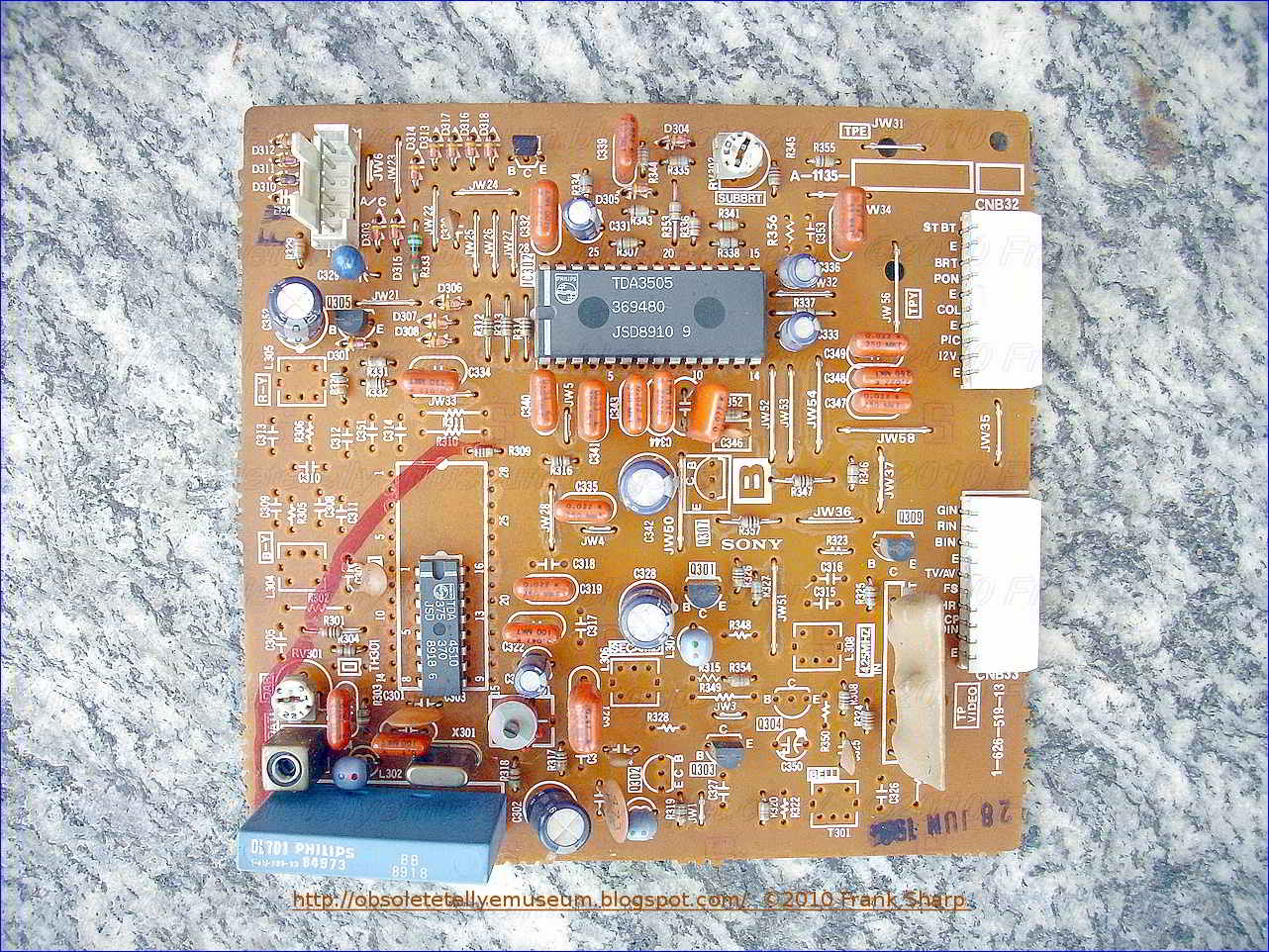


The chassis BE-1 is straightforward completing the set in all parts and was fitted even in 21 in. sets.
GENERAL DESCRIPTION
The TDA3505 and TDA3506 are monolithic integrated circuits which perform video control functions in a PAL/SECAM
decoder. The TDA3505 is for negative colour difference signals −(R-Y), −(B-Y) and the TDA3506 is for positive colour
difference signals +(R-Y), +(B-Y).
The required input signals are: luminance and colour difference (negative or positive) and a 3-level sandcastle pulse for
control purposes. Linear RGB signals can be inserted from an external source. RGB output signals are available for
driving the video output stages. The circuits provide automatic cut-off control of the picture tube.
Features
• Capacitive coupling of the colour difference and
luminance input signals with black level clamping in the
input stages
• Linear saturation control acting on the colour difference
signals
• (G-Y) and RGB matrix
• Linear transmission of inserted signals
• Equal black levels for inserted and matrixed signals
• 3 identical channels for the RGB signals
• Linear contrast and brightness controls, operating on
both the inserted and matrixed RGB signals
• Peak beam current limiting input
• Clamping, horizontal and vertical blanking of the three
input signals controlled by a 3-level sandcastle pulse
• 3 DC gain controls for the RGB output signals (white
point adjustment)
• Emitter-follower outputs for driving the RGB output
stages
• Input for automatic cut-off control with compensation for
leakage current of the picture tube.
PINNING
PIN
DESCRIPTION
1
red output
2
green storage capacitor for cut-off control
3
green output
4
blue storage capacitor for cut-off control
5
blue output
6
positive supply voltage (+ 12 V)
7
blue storage for brightness
8
green storage for brightness
9
red storage for brightness
10
sandcastle pulse input
11
fast switch for RGB inputs
12
blue input (external signal)
13
green input (external signal)
14
red input (external signal)
15
luminance input
16
saturation control input
17
colour difference input − (R-Y) or + (R-Y) respectively
18
colour difference input − (B-Y) or + (B-Y) respectively
19
contrast control input
20
brightness control input
21
white point adjustment, blue
22
white point adjustment, green
23
white point adjustment, red
24
ground (0 V)
25
control input for peak beam current limiting
26
automatic cut-off control input
27
storage capacitor for leakage current
28
red storage capacitor for cut-off control.
Notes
1.
< 110 mA after warm-up.
2.
Values are proportional to the supply voltage.
3.When V11-24< 0,4 V during clamping time - the black levels of the inserted RGB signals are clamped on the black
levels of the internal RGB signals.
When V11-24> 0,9 V during clamping time - the black levels of the inserted RGB signals are clamped on an internal
DC voltage (correct clamping of the external RGB signals is possible only when they are synchronous with the
sandcastle pulse).
4.
When pins 21, 22 and 23 are not connected, an internal bias voltage of 5,5 V is supplied.
5.
Automatic cut-off control measurement occurs in the following lines after start of the vertical blanking pulse:
line 20: measurement of leakage current (R + G + B)
line 21: measurement of red cut-off current
line 22: measurement of green cut-off current
line 23: measurement of blue cut-off current
6.
Black level of the measured channel is nominal; the other two channels are blanked to ultra-black.
7.
All three channels blanked to ultra-black.
The cut-off control cycle occurs when the vertical blanking part of the sandcastle pulse contains more than 3 line
pulses.
The internal blanking continues until the end of the last measured line.
The vertical blanking pulse is not allowed to contain more than 34 line pulses, otherwise another control cycle begins.
8.
The sandcastle pulse is compared with three internal thresholds (proportional to VP) and the given levels separate
the various pulses.
9.
Blanked to ultra-black (−25%).
10. Pulse duration ≥ 3,5 µs.
PHILIPS TDA4510 PAL decoder:
GEN
ERAL DESCRIPTION
The TDA4510 is a colour decoder for the PAL standard, which is pin sequent compatible with multistandard decoder
TDA4555 and also pin compatible with NTSC decoder TDA4570. It incorporates the following functions:
Chrominance part
• Gain controlled chrominance amplifier with operating point control stage
• Chrominance output stage for driving the 64 µs delay line
• Blanking circuit for the colour burst signal
• Automatic chrominance control (ACC) with sampled rectifier during burst-key
Oscillator and control voltage part
• Reference oscillator for double subcarrier frequency
• Gated phase comparison
• Identification demodulator and automatic colour killer
• Sandcastle pulse detector
• Service switch
Demodulator part
• Two synchronous demodulators for the (B-Y) and (R-Y) signals
• PAL flip-flop and PAL switch
• Colour switching stages
• Separate colour switching output
• (B-Y) and (R-Y) signal output stages
• Internal filtering of residual carrier.
FUNCTIONAL DESCRIPTION
DIVIDER STAGES
The divider stages provide −(R-Y) and −(B-Y) reference signals with the correct 90 degrees relation for the demodulators.
PHASE COMPARATOR
The phase comparator compares the −(R-Y) reference signal with the burst pulse and controls the frequency and phase
of the reference oscillator.
IDENTIFICATION DEMODULATOR
The identification demodulator delivers a positive going identification signal for PAL-signals at pin 14, also used for the
automatic colour-killer.
SERVICE SWITCH
The service switch has two functions. The first position (V14-3< 1 V) allows the adjustment of the reference oscillator.
Therefore the colour is switched on and the burst for the oscillator PLL is switched off. The second position (V14-3> 5 V)
switches the colour on and the output signals can be observed.
SANDCASTLE PULSE DETECTOR
Sandcastle pulse detector for burst-gate, line and blanking (horizontal and vertical) pulse detection. The vertical part of
the sandcastle pulse is needed for the internal colour-on and colour-off delay.
PULSE PROCESSING PART
Pulse processing part which shall prevent a premature switching on of the colour. The colour-on delay, two or three field
periods after identification of the PAL signal, is achieved by a counter. The colour is switched off immediately or at the
latest one field period after disappearance of the identification voltage.
SONY Automatic pre-programming system for TV receiver/ Automatically presetting channel Program selecting system :"A channel selecting system for use in a receiver having a voltage controlled tuning element which has an automatic channel presetting function which utilizes a pulse generator and a binary counter connected to the generator to count the pulses and to generate a binary coded output in accordance with the sum of the pulses. A digital-to-analog converter changes the binary coded output into a linearly increasing tuning sweep voltage which in turn conditions the voltage controlled tuning element to scan the frequency range of the tuner as the tuning voltage increases. As the frequencies are scanned, a detector, connected to the tuning element, senses the presence of a broadcast channel. When a channel is detected, the scan is interrupted and a binary memory is utilized to store the binary coded output which corresponds to the frequency of the detected broadcast channel. A control gate signal generator driven by the detector controls the pulse generator and memory such that the scan is continued until the entire frequency range has been scanned. Channel selection is accomplished by switch means actuatable to address the memory to read out a selected binary code output corresponding to the channel desired which causes the converter to generate a voltage to condition the tuning element to tune to the desired frequency. The voltage control tuning element may comprise several different elements, one for each of a plurality of different frequency ranges. Means are provided for selecting an appropriate tuner such that channels from any of the frequency ranges may be selected. "
An automatic tuning scheme for use in TV receivers includes a start/stop circuit which creates a search start signal and a search stop signal upon the receipt of a search start instruction and a detected incoming signal, respectively, a tuning voltage generator which generates a gradually varying tuning voltage under control of the search start signal and search stop signal, and a memory circuit for storing the tuning voltage from the generator when desired. The tuning voltage stored in the memory circuit is supplied to a tuner including a well known voltage-sensitive capacitance diode.
1. An automatic tuning scheme for use in TV receivers including an AFT detector comprising:
start/stop circuit means for creating a search start signal and a search stop signal upon the receipt of a search start instruction and the presence of a detected incoming signal, respectively, the presence of a detected incoming signal being determined at least in part in response to an output of said AFT detector;
tuning voltage generator means for generating a gradually varying tuning voltage under control of the search start signal and search stop signal;
memory circuit means for storing the tuning voltage from said tuning voltage generator means;
signal decision circuit means for determining whether the detected incoming signal is a true television signal including a television synchronizing signal by detecting the presence of the television synchronizing signal and the search stop signal, said signal decision circuit means providing a memory store instruction for the memory circuit means in the presence of the true television signal and providing a search re-start instruction for the start/stop circuit means in the absence of the true television signal, the tuning voltage stored in the memory circuit means being supplied to a tuner including a voltage-sensitive capacitance diode.
2. The automatic tuning scheme according to claim 1 further comprising a memory skip circuit for inhibiting the supply of the memory store instruction to the memory circuit and skipping an undesired broadcasting station. 3. An automatic tuning scheme for use in TV receivers including an AFT detector comprising:
start/stop circuit means for creating a search start signal and a search stop signal upon the receipt of a search start instruction and a detected incoming signal, respectively;
tuning voltage generator means for generating a gradually varying tuning voltage under control of the search start signal and search stop signal;
memory circuit means for storing the tuning voltage from the tuning voltage generator means
means for detecting the presence of synchronizing signals within the detected incoming signal;
noise skip circuit means which determines whether the detected synchronizing signal is a true synchronizing signal or noise and provides a search re-start instruction for the start/stop circuit means in the presence of noise; and
signal decision circuit means for determining whether there is a true television signal by counting the number of the true synchronizing signals derived from the noise skip circuit means and counting a predetermined number of the true synchronizing signals in a predetermined period of time, and then providing a memory store instruction for the memory circuit means in the presence of the true television signal and a search re-start instruction to the start/stop circuit means in the absence thereof, the tuning voltage stored in the memory circuit means being supplied to a tuner.
4. In an automatic tuning scheme for use in TV receivers including an AFT detector, which produces search start and stop signals upon receipt of a search start instruction and a detected incoming signal, a combination comprising:
means for detecting the presence of synchronizing signals within the detected incoming signal;
noise skip circuit means for determining whether the synchronizing signal is a true synchronizing signal or noise and provides a search restart instruction to said tuning scheme in the presence of noise; and
means for adjusting a skip level in the noise skip circuit means in accordance with the intensity of the detected incoming signal.
5. An automatic tuning scheme for use in TV receivers including an AFT detector comprising:
start/stop circuit means which creates a search start signal and a search stop signal upon the receipt of a search start instruction and a detected incoming signal, respectively;
tuning voltage generator means for generating a gradually varying tuning voltage under control of the search start signal and search stop signal;
memory circuit means for storing the tuning voltage from the generator, the tuning voltage stored in the memory circuit means being supplied to a tuner;
speed changer means for reducing the rate of variation in the tuning voltage derived from the tuning voltage generator means to enable a low speed searching operation slower than that of the normal searching operations when detecting an AFT detector output;
means for detecting the presence of synchronizing signals within the detected incoming signal; and
means for determining wheth
er the synchronizing signal is a true
synchronizing signal or noise and providing a search re-start
instruction to said tuning scheme in the presence of noise.6. An automatic tuning scheme for use in TV receivers including an AFT detector comprising:
start/stop circuit means for creating a search start signal and a search stop signal upon the receipt of a search start instruction and a detected incoming signal, respectively;
tuning voltage generator means for generating a gradually varying tuning voltage under control of the search start signal and search stop signal;
memory circuit means for storing the tuning voltage from the tuning voltage generator means, the tuning voltage stored in the memory circuit means being supplied to a tuner; and
speed changer means for reducing the rate of variation in the tuning voltage derived from the tuning voltage generator means to enable a low speed searching operation slower than that of the normal searching operation when detecting an AFT detector output, the direction of variation of the tuning voltage being reversed in accordance with the polarity of the AFT detector output.
7. An automatic tuning scheme for use in TV receivers including an AFT detector comprising:
start/stop circuit means for creating a search start signal and a search stop signal upon the receipt of a search start instruction and a detected incoming signal, respectively;
tuning voltage generator means for generating a gradually varying tuning voltage under control of the search start signal and search stop signal;
memory circuit means for storing the tuning voltage from the tuning voltage generator means, the tuning voltage stored in the memory circuit means being supplied to a tuner;
out-of-tuning detector means for supplying a search re-start signal to the start/stop circuit means when detecting the out-of-tuning condition;
means for detecting the presence of synchronizing signals within the detected incoming signal; and
means for determining whether the synchronizing signal is a true synchronizing signal or noise and providing a search re-start instruction to said tuning scheme in response thereto.
8. The automatic tuning scheme according to claim 7 wherein the out-of-tuning condition is sensed by comparing the AFT detector output to a given reference voltage. 9. An automatic tuning scheme for use in TV receivers including an AFT detector comprising:
start/stop circuit means for creating a search start signal and a search stop signal upon the receipt of a search start instruction and a detected incoming signal, respectively;
tuning voltage generator means for generating a gradually varying tuning voltage under control of the search start signal and search stop signal;
means for detecting the presence of synchronizing signals within the detected incoming signal; and
means for determining whether the detected synchronizing signal is a true synchronizing signal or noise and providing a search re-start instructions to said tuning scheme in the presence of noise.
10. The automatic tuning scheme according to claim 9 further comprising alarm means enabled by the tuning instruction for notifying the operator of the automatic tuning operation. 11. The automatic tuning scheme according to claim 10 wherein said alarm means release alarm signals in the form of sound. 12. The automatic tuning scheme according to claims 3, 4, 5, 6, 7, or 9 wherein the reception of a true television signal is determined by the use of said true synchronizing signal and an AFT output.
Description:
BACKGROUND OF THE INVENTION
The present invention relates to an automatic pre-programming tuning circuit which performs tuning operation automatically.
It is customary to perform the tuning operations in TV receivers while a viewer manually rotates a tuning knob. However, the tuning operation is bothersome particularly in case of the continuously varying tuning operation such as in UHF reception. Though tuning operation is considerably simpler in case of TV receivers of the recently developed touch control type or remote control type, it is difficult for a non-skilled person the to preset tuning operation, namely, to adjust the tuning frequencies for respective broadcasting stations before starting to watch a TV receiver.
SUMMARY OF THE INVENTION
Accordingly, it is an object of the present invention to provide an automatic tuning scheme which enables automatic preselectable tuning operation by sequentially memorizing tuning voltages of respective automatically selected broadcasting channels.
In its broadest aspect, an automatic tuning device of the present invention comprises a tuning voltage generator which generates a tuning voltage gradually variable during tuning operation, a memory circuit which receives the tuning voltage derived from the generator upon receipt of normal reception signals and memorizes a plurality of discrete tuning voltages each associated with a respective one of normal reception signal corresponding to a serviceable broadcasting station and means for picking up selectively one of the discrete tuning voltages from the memory circuit and supplying it to a tuner.
BRIEF DESCRIPTION OF THE DRAWINGS
Other objects and attendant advantages of the present invention will be easily appreciated as the same becomes better understood by reference to the following detailed description when considered in conjunction with the accompanying drawings in which like reference numerals designate like part throughout the figures thereof, and wherein:
FIG. 1 is a schematic diagram of the automatic tuning apparatus embodying the present invention;
FIG. 2 is a more detailed circuit diagram of the automatic tuning apparatus shown in FIG. 1;
FIG. 3 is a schematic diagram of another embodiment of the present invention;
FIGS. 4 and 5 are a circuit diagram and a waveform diagram showing a noise skip circuit included in FIG. 3 embodiment;
FIG. 6 is an improvement in the noise skip circuit shown in FIGS. 4 and 5;
FIGS. 7 and 8 are embodiments effective to modify the searching speed in the automatic tuning apparatus;
FIGS. 9 through 11 are refresh means effective in the automatic tuning apparatus of the present invention;
FIG. 12 shows another embodiment including a memory skip circuit effective in the automatic tuning apparatus;
FIGS. 13 and 14 show alarm means effective in the automatic tuning apparatus.
DETAILED DESCRIPTION OF THE INVENTION
A basic circuit of a TV recei ver
having an automatic tuning scheme implemented with the present
invention is shown in FIG. 1, which includes an antenna 1, a tuner 2, an
intermediate frequency (IF) circuit 3, an automatic fine tuning (AFT)
circuit 4, a video circuit 5, a synchronizing separator 6, a
deflection circuit 7, a picture tube 8. According to the present
invention, a start/stop circuit 9, a tuning voltage generator 10, a
memory circuit 11 and a signal decision circuit 12 are further
provided to form the automatic tuning scheme of the present invention.
ver
having an automatic tuning scheme implemented with the present
invention is shown in FIG. 1, which includes an antenna 1, a tuner 2, an
intermediate frequency (IF) circuit 3, an automatic fine tuning (AFT)
circuit 4, a video circuit 5, a synchronizing separator 6, a
deflection circuit 7, a picture tube 8. According to the present
invention, a start/stop circuit 9, a tuning voltage generator 10, a
memory circuit 11 and a signal decision circuit 12 are further
provided to form the automatic tuning scheme of the present invention.
It will be noted that the tuner 2 can be implemented with a well known electronic tuning circuit which includes a voltage-sensitive capacitance diode as disclosed in U.S. Pat. No. 3,233,179 entitled "AUTOMATIC FINE TUNNING CIRCUIT USING CAPACITANCE DIODES" issued on Feb. 1, 1966.
If the start/stop circuit 9 is given a search start command or au automatic tuning instruction prior to effecting of the preset tuning operation, then the start/stop circuit 9 will develop a search start pulse which is turn is supplied to the tuning voltage generator 10. Under the circumstance the tuning voltage generator 10 develops a sweep voltage or staircase voltage which is gradually rising or dropping during the automatic tuning operation. The sweep or staircase voltage is supplied as the tuning voltage to the tuning capacitance diode in the tuner 2 by way of the memory circuit 11. This implies that the reception frequency in the tuner 2 is gradually varied.
 In this way, when the television
signal of a specific broadcasting channel is received, the television
video signal is derived from the IF circuit 3 and the synchronizing
signal from the synchronizing separator 6. These signals are applied
to the start/stop circuit 9. Meantime, the AFT detector output is
derived from the AFT circuit 4 and supplied to the start/stop circuit
9.
In this way, when the television
signal of a specific broadcasting channel is received, the television
video signal is derived from the IF circuit 3 and the synchronizing
signal from the synchronizing separator 6. These signals are applied
to the start/stop circuit 9. Meantime, the AFT detector output is
derived from the AFT circuit 4 and supplied to the start/stop circuit
9.
More particularly, when the television signal is accurately received, the AFT detector output voltage will change in polarity so that the start/stop circuit 9 is permitted to develop a search stop pulse and the vertical synchronizing signal. In the given example the vertical synchronizing signal may serve as the search stop pulse. The search stop pulse is supplied to the tuning voltage generator 10, barring the generator 10 from developing the sweep or staircase voltage. The voltage at this moment remains unchanged since then and keeps being supplied as the tuning voltage to the tuner 2 via the memory circuit.
The vertical synchronizing signal derived from the start/stop circuit 9 is supplied to the signal decision circuit 12 to determine as to whether the signal being received is a normal or true television signal. If the affirmative answer is given, then the signal decision circuit 12 will issue a memory instruction which in turn is supplied to the memory circuit 11 so that the instantaneous tuning voltage derived from the generator 10 is stored within the memory circuit 11.
Contrarily, if a false synchronizing signal is derived from the start/stop circuit 9, then the signal decision circuit 12 reacts to it so that the circuit 12 issues a search re-start pulse. This is supplied to the start/stop circuit 9 to repeat the same procedure as when executing the first search start pulse. The procedure is repeated in this manner until the start/stop circuit 9 recognizes a true television vertical synchronizing signal or accurate reception is available by the tuner 2.
In other words, the memory instruction is not issued from the signal decision circuit 12 until the optimum reception state is guaranteed. Upon issuance of the memory instruction the instantaneous tuning voltage is stored in the memory circuit 11 and subsequently supplied to the tuner 2.
Once the preset tuning operation (i,e, the presetting of the optimum reception
frequency) has been completed for the specific broadcasting channel,
the tuning voltage stored in the memory circuit 11 will be
automatically supplied to the tuner in response to release of a tuning
instruction from an operational panel of the known touch control type
or remote control type. The searching procedure is not required at
this time.
the optimum reception
frequency) has been completed for the specific broadcasting channel,
the tuning voltage stored in the memory circuit 11 will be
automatically supplied to the tuner in response to release of a tuning
instruction from an operational panel of the known touch control type
or remote control type. The searching procedure is not required at
this time.
It is obvious that the memory circuit 11 shown in FIG. 1 includes a predetermined number of memory elements the number of which corresponds to the number of serviceable broadcasting stations. The same searching or presetting procedure is repeated when it is desired to search and memorize a predetermined number of discrete tuning voltages prior to use of a TV receiver.
As noted earlier, when the search start instruction is given and the search start signal is released from the start/stop circuit 9, the tuning voltage generator 10 starts generating the sweep voltage (or the staircase voltage), which is supplied to the tuner 2 via the memory circuit 11 while showing a gradual variation. Alternatively, the gradually varying voltage may be supplied to the tuner 2 directly. If the search stop signal is derived from the start/stop circuit 9 upon receipt of the television signal, the sweep voltage generating function of the tuning voltage generator will come to a halt. The instantaneous tuning voltage supplied to the tuner 2 is held unchanged for a while.
At this time the signal decision circuit 12 decides whether the received signal is true or false. After confirming the presence of the true television signal, the memory instruction is issued for the memory circuit 11 so that the tuning voltage available from the tuning voltage generator 10 is held within the memory circuit 10 to complete the presetting of the optimum reception frequency for the specific television station.
On the contrary, when the signal decision circuit 12 does not sense the presence of the true television signal, the search re-start signal is issued for the start/stop circuit 9 to start the above mentioned operation again. Each time the memorizing operation or the tuning frequency presetting operation is completed in the memory circuit 11 for a specific one of broadcasting stations, the search start instruction is issued again for the start/stop circuit 9. Eventually, a plurality of discrete tuning voltages are stored in sequence in the memory circuit 9, completing the over-all loading operation of the discrete tuning voltages.
FIG. 2 shows a detailed way of implementation of the present invention briefly described with respect to FIG. 1. When a search switch SW1 is turned on, a latch FF1 is placed to the set state with the Q output at a high level "H" and the Q output at a low level "L". A gate G3
is enabled such that clock pulses from a clock pulse generator 13 are
sequentially supplied to a counter 14 to increment it at a high
speed. The output of the counter 14 is supplied to a digital-to-analog
converter 15 which converts the output of the counter 14 into a DC
voltage correspondingly. This DC voltage is supplied as the tuning
voltage to the tuner 2. Therefore, the gradually rising sweep voltage is
transferred from the digital-to-analog converter 15 to the tuner 2 so
that the reception frequency in the tuner 2 is gradually varied in
the ascending order.
of the present invention briefly described with respect to FIG. 1. When a search switch SW1 is turned on, a latch FF1 is placed to the set state with the Q output at a high level "H" and the Q output at a low level "L". A gate G3
is enabled such that clock pulses from a clock pulse generator 13 are
sequentially supplied to a counter 14 to increment it at a high
speed. The output of the counter 14 is supplied to a digital-to-analog
converter 15 which converts the output of the counter 14 into a DC
voltage correspondingly. This DC voltage is supplied as the tuning
voltage to the tuner 2. Therefore, the gradually rising sweep voltage is
transferred from the digital-to-analog converter 15 to the tuner 2 so
that the reception frequency in the tuner 2 is gradually varied in
the ascending order.
When the television signal of a specific broadcasting station is received, the television video signal is derived from the IF circuit 3 and the horizontal and vertical synchronizing signals are derived from the synchronizing separator 6. In the case where the detector output voltage from the AFT circuit 4 is positive, a gate G2 is enabled to place the latch FF1 into the reset state. At the moment the Q and Q outputs of the latch FF1 are respectively inverted into "L" and "H" levels. A gate G3 is disabled to stop supply of the clock pulses to the counter 14 so that the digital-to-analog converter 15 supplies the tuner 2 with the output voltage of a fixed value. In other words, the searching operation comes to a halt.
When the true television signal is being received, the horizontal synchronizing pulse derived from the synchronizing separator 6 is in phase with the flyback pulse derived from the deflection circuit 7. A transistor Tr1 is turned on in reponse to the horizontal synchronizing pulse with an increase in the emitter potential thereof. Gates G4 and G5 are enabled so that the vertical synchronizing pulse is supplied as the memory instruction to the memory circuit 11 via these gates G4 and G5. At this moment the output of the counter 14 is loaded into the first address of the memory circuit 11 in a digital fashion.
However, if the signal being received is not the true television signal, then the horizontal synchronizing pulse will neither be synchronous with the flyback pulse nor will the transistor Tr1 be turned on. Even though the vertical synchronizing pulse from the synchronizing separator 6 or the false synchronizing pulse forces the latch FF1 into the reset state, the gate G5 is never enabled but the gate G6 is enabled. The pulse transferred via the gate G6 is supplied as the search re-start pulse to the latch FF1 which then resorts to the reset state again to restart the searching procedure.
After the searching/memory operation has been completed for a specific one of broadcasting stations, the memory circuit 11 releases the search start pulse again, which is then supplied to the latch FF1 via the gate G1 to set the latch FF1.
The same operation is thus repeated. A different tuning voltage of the next suceeding station is digitally stored at the second address of the memory circuit 11. In this way, a predetermined number of discrete tuning voltages are digitally stored in sequence until the end of the presetting operation.
Once the presetting operation has been accomplished, all that is necessary for the operator to do is to select a desired one of channel selection switches 161 through 16n. Then, digital information indicative of the tuning voltage previously stored at its associated address of the memory circuit 11 is called forth in accordance with its associated selection codes within an address specifying circuit 17. The digital information is applied via the counter 14 to the digital-to-analog converter 15 which decodes it into the analog tuning voltage. The tuning voltage is supplied to the tuning capacitance diode included within the tuner 2.
FIG. 3 shows another example of the tuning scheme furth er
comprising a noise skip circuit. As described above, when the true
television signal is received, the output from the AFT detector will
change in polarity and upon such change the television synchronizing
signal will be derived from the start/stop circuit 9. This
synchronizing signal is supplied to a noise skip circuit 18 to decide
whether or not this is the true television vertical synchronizing
signal. Particularly when the true vertical synchronizing signal is
confirmed, this is applied to the signal decision circuit 12 and
simultaneously applied as the search stop pulse to the tuning voltage
generator 10. Contrarily, when concluded as noise and not the
synchronizing signal, this will be supplied as the re-start pulse to
the start/stop circuit 9. This permits the recurring of the same
operation as when the search start instruction is issued for the first
time. In the given example, the vertical synchronizing signal obtained
from the noise skip circuit 18 is utilized as the search stop pulse.
er
comprising a noise skip circuit. As described above, when the true
television signal is received, the output from the AFT detector will
change in polarity and upon such change the television synchronizing
signal will be derived from the start/stop circuit 9. This
synchronizing signal is supplied to a noise skip circuit 18 to decide
whether or not this is the true television vertical synchronizing
signal. Particularly when the true vertical synchronizing signal is
confirmed, this is applied to the signal decision circuit 12 and
simultaneously applied as the search stop pulse to the tuning voltage
generator 10. Contrarily, when concluded as noise and not the
synchronizing signal, this will be supplied as the re-start pulse to
the start/stop circuit 9. This permits the recurring of the same
operation as when the search start instruction is issued for the first
time. In the given example, the vertical synchronizing signal obtained
from the noise skip circuit 18 is utilized as the search stop pulse.
In this way the search stop pulse is developed from noise skip circuit 18 and sent to the tuning voltage generator 10, stopping the generator
10 from generating the sweep voltage. The instantaneous voltage is
thereafter kept and sent to the tuner 2 via the memory circuit 11.
Under these circumstances the signal decision circuit 12 determines
again whether the vertical synchronizing signal developed from the
start/stop circuit 9 is the true television synchronizing signal.
By way of example, the signal decision circuit 12 may be adapted to count the number of the synchronizing signals and determine whether a predetermined number of the synchronizing signals are present during a given period of time. If the true synchronizing signal is sensed, then the signal decision circuit 12 will release the memory instruction, permitting the memory circuit 11 to store the tuning voltage supplied from the generator 10.
Nevertheless, even if the noise skip circuit 18 delivers the false synchronizing signal inadvertently, the signal decision circuit 12 never overlooks it so that the circuit 12 issues the search re-start pulse. The start/stop circuit 9 receives such pulse to repeat the above mentioned operation. In other words, the operation is repeated to assure the optimum reception condition until the true television synchronizing signal is available from the start/stop circuit 9 and the noise skip circuit 18. The memory instruction will be issued immediately after the optimum reception condition is reached.
Details of the noise skip circuit 18 are shown in FIG. 4. This is split into three major portions: an integration circuit portion 21 consisting of resistors R1 and R2 and capacitors C1 and C2 ; a noise detection circuit portion 22 consisting of transistors Q1, Q2 and Q3, a diode D1 and so on; and a synchronizing signal amplifier portion 23 consisting of a transistor Q4 and so on. Assume now that the true television synchronizing signal (with negative polarity) as viewed from FIG. 5 a is derived from the start/stop circuit 9. This signal is integrated with the integration circuit portion 21 as shown in FIG. 5 b . The base bias voltage of the first stage transistor Q1 in the noise detector portion 22 is fixed, say at approximately 0.3 volts, by the resistors R3, R4 and R5 and the diode D1. Thus, this signal at the positive polarity side is extremely shallow and the transistor Q1 is placed into the cut off state as long as the genuine vertical synchronizing signal is derived. The remaining transistors Q2 and Q3 are also placed into the cut off state. Therefore, the noise detector portion 22 does not deliver the output signal or the search stop pulse. The vertical synchronizing pulse as shown in FIG. 5 c is applied to the base of the transistor Q4 via the capacitor C3 for amplification. The vertical synchronizing signal with the positive polarity as shown in FIG. 5 d is developed at the collector of the transistor Q4 and supplied to the signal decision circuit 12 and as the search stop pulse to the tuning voltage generator 10.
On the other hand, if the noise signal, for example, as shown in FIG. 5 e is derived from the start/stop circuit 9, then this will be integrated
with the integration circuit portion 21. The result is shown in FIG. 5 f
, which has both positive and negative polarity components. Since the
positive polarity component is well above the conduction level (say,
0.6 volts) of the transistor Q1, the transistor Q1 is turned on whenever an the transistors Q2 and Q3 are also turned on. The signal appearing at the emitter of the transistors Q3 is shown in FIG. 5 h and returned as the search re-start pulse to the start/stop circuit 9.
derived from the start/stop circuit 9, then this will be integrated
with the integration circuit portion 21. The result is shown in FIG. 5 f
, which has both positive and negative polarity components. Since the
positive polarity component is well above the conduction level (say,
0.6 volts) of the transistor Q1, the transistor Q1 is turned on whenever an the transistors Q2 and Q3 are also turned on. The signal appearing at the emitter of the transistors Q3 is shown in FIG. 5 h and returned as the search re-start pulse to the start/stop circuit 9.
By the action of the noise skip circuit 18. Whether the signal derived from the start/stop circuit 9 is the true synchronizing signal or noise is determined by the positive voltage level of that signal. Then, the synchronizing signal is supplied to the signal decision circuit 12 and the tuning voltage generator 10, while the noise is supplied as the search re-start pulse to the start/stop circuit. As shown in FIG. 6, a skip level adjusting variable resistor VR1 installed in the noise detector portion 22 makes the above mentioned positive voltage level freely variable. It also becomes possible to supply the noise as the search re-start pulse to the start/stop circuit 9 when the normal television synchronizing signal is received but relatively strong noise is superimposed thereon.
Within the tuning scheme having the noise skip circuit, there is no opportunity inadvertently the tuning voltage generator 10 with the search stop instruction due to noise. In addition, only broadcasting stations with comparatively strong television signals can be preset in sequence while skipping ones with comparatively weak television signals. Although in the illustrated example the noise skip level is manually variable through the use of the variable resistor VR1, it is noted that the skip level can be varied in response to the intensity of the television signals being received by applying an AGC voltage thereto.
Details of modifications in the start/stop circuit 9 and the tuning voltage generator 10 are shown in FIG. 7 wherein the search speed is variable.
Provided that the search start instruction or the search restart pulse is supplied via an OR gate 34 to a reset input terminal of an R-S type latch 33, the latch 33 will be in the reset state so that the Q output thereof assumes a "H" level to enable an AND gate 35. Another latch 39 of the R-S type 39 is also placed into the reset state in response to the search start instruction or the search re-start pulse. The Q oupu t
of the latch 39 assumes a "L" level and the Q output assumes a "H"
level, enabling an AND gate 40. At this time clock pulses of, for
example, 320 Hz are generated via an AND gate 40, an OR gate 47 and an
AND gate 35 from a high speed clock pulse generator 36 and supplied to a
counter 42 in the tuning voltage generator 10. The count of the
counter 42 varies sequentially at a relatively high rate and is
converted through a digital-to-analog converter 43. As a consequence,
the converter 43 develops a gradually rising or dropping DC voltage,
which is supplied to the tuner 2 via the memory circuit 11. A rate of
variations in the tuning voltage derived from the generator 43 is
relatively high and the searching procedure is carried out at a high
speed.
t
of the latch 39 assumes a "L" level and the Q output assumes a "H"
level, enabling an AND gate 40. At this time clock pulses of, for
example, 320 Hz are generated via an AND gate 40, an OR gate 47 and an
AND gate 35 from a high speed clock pulse generator 36 and supplied to a
counter 42 in the tuning voltage generator 10. The count of the
counter 42 varies sequentially at a relatively high rate and is
converted through a digital-to-analog converter 43. As a consequence,
the converter 43 develops a gradually rising or dropping DC voltage,
which is supplied to the tuner 2 via the memory circuit 11. A rate of
variations in the tuning voltage derived from the generator 43 is
relatively high and the searching procedure is carried out at a high
speed.
While a specific television signal is received, the detector output is derived from the AFT circuit 4 and the vertical synchronizing signal is derived from the synchronizing separator 6. When an AFT negative output detector 44 senses the AFT detector output of the negative polarity, the output of the detector 44 increases to a "H" level. The AND gate 45 is enabled so that the vertical synchronizing signal is supplied to a set input terminal of the R-S type latch 39. The latch 39 is placed into the set state with the Q output thereof having a "H" level and the Q output thereof having a "L" level. The AND gate 40 is disabled concurrently with the enabling of the AND gate 46. Under these circumstances clock pulses of, for example, 160 Hz from a low speed clock pulse generator 47 are supplied
to the counter 42 via the AND gate 46, the OR gate 41 and the AND
gate 35. The counter 42 performs the counting operation at a low
speed. A rate of variations in the tuning voltage or the DC voltage
obtainable from the digital-to-analog converter 43 is reduced to
one-half its initial rate and the searching procedure is carried out at
a low speed.
If the polarity of the AFT detector output changes from negative to positive during the low speed searching operation, then the output of an AFT positive output detector will increase to a "H" level. The AND gate 38 is enabled and the vertical synchronizing signal is supplied via the AND gates 38 and 48 to the set input terminal of the R-S type latch 33 (the AND gate 48 is now enabled because of the Q output of the latch 39 at a "H" level). The latch 33 is therefore set. As a result, the Q output of the latch 33 changes to a "L" level to disable the AND gate 35. The counter 42 is supplied with the clock pulses no longer. Afterward, the count of the counter 42 remains unchanged and the tuning voltage derived from the digital-to-analog converter 43 is held at a fixed value. The searching operation comes to a stop.
Then, when the search start instruction of the search re-start pulse is issued again, the latch 33 and 39 are reset to enable AND gates 35 and 40. The clock pulses from the high speed clock pulse generator 36 are supplied to the counter 42, restarting the searching operation.
Another modification in the start/stop circuit 9 and the tuning voltage generator 10 is shown in FIG. 8. When the search sta rt
instruction or the search re-start pulse is supplied to the reset
input terminal of the latch 33 via the OR gate 34, the Q output of the
latch 33 in the reset state will assume a "H" level with the AND gates
35 and 49 enabled. The other latches 39 and 50 are also reset in
response to the search start instruction or the search re-start pulse
with the Q outputs thereof at a "L" level and the Q outputs thereof a
"H" level. The AND gate 40 is enabled while the AND gate 46 and 51
remain disabled. The 320 Hz clock pulses from the high speed clock
pulse generator 36 are derived via the AND gate 40, the OR gate 41 and
the AND gate 35 and supplied to a count up input terminal of an
up/down counter 42' in the tuning voltage generator 10. The counter
42' is sequentially incremented at a high speed, the count of which is
supplied to the digital-to-analog converter 43. As a result, the
converter 43 develops a gradually rising DC voltage which is supplied
as the tuning voltage to the tuner 2 via the memory circuit 11. In this
case variations in the tuning voltage are comparatively quicker and
the searching operation is carried out by the increase of the local
oscillation frequency.
rt
instruction or the search re-start pulse is supplied to the reset
input terminal of the latch 33 via the OR gate 34, the Q output of the
latch 33 in the reset state will assume a "H" level with the AND gates
35 and 49 enabled. The other latches 39 and 50 are also reset in
response to the search start instruction or the search re-start pulse
with the Q outputs thereof at a "L" level and the Q outputs thereof a
"H" level. The AND gate 40 is enabled while the AND gate 46 and 51
remain disabled. The 320 Hz clock pulses from the high speed clock
pulse generator 36 are derived via the AND gate 40, the OR gate 41 and
the AND gate 35 and supplied to a count up input terminal of an
up/down counter 42' in the tuning voltage generator 10. The counter
42' is sequentially incremented at a high speed, the count of which is
supplied to the digital-to-analog converter 43. As a result, the
converter 43 develops a gradually rising DC voltage which is supplied
as the tuning voltage to the tuner 2 via the memory circuit 11. In this
case variations in the tuning voltage are comparatively quicker and
the searching operation is carried out by the increase of the local
oscillation frequency.
Under these circumstances, when the television signal is received, The AFT circuit 4 develops the AFT detector output and the synchronizing separator 6 develops the vertical synchronizing signal. If there is the negative output sensed by the AFT negative output detector 44, the output of the detector 44 will assume a "H" level to enable the AND gate 45. The vertical synchronizing signal is supplied to the set input terminal of the R-S type latch 39 via the AND gate 45, setting the same. Since the Q and Q outputs of the latch 39 assume "H" and "L" levels respectively, the AND gate 46 is enabled and the AND gate 40 is disabled. The clock
pulses with 160 Hz from the low frequency clock pulse generator 47 are
supplied via the AND gate 46, the OR gate 41 and the AND gate 35 to
the count up input terminal of the counter 42' to execute the counting
operation at a relatively low speed. The DC voltage or the tuning
voltage derived from the digital-to-analog converter 43 shows
variations at a rate which is reduced to one half its initial rate. The
searching operation is carried out with low speed in order to
eventually increase the local oscillation frequency.
Thereafter,
when the polarity of the AFT detector output changes from negative to
positive during the slow searching operation, the output of the AFT
positive output detector 37 increases to a "H" level, enabling the AND
gate 38 such that the vertical synchronizing signal is supplied to a
set input terminal of an R-S type latch 50 therethrough. The result is
that the latch 50 is placed into the set state with the Q output
thereof at a "H" level and the Q output thereof at a "L" level. An AND
gate 57 is enabled and the AND gates 40 and 46 are disabled.
Therefore, clock pulses with, for example, 20 Hz are derived from an
extremely low speed clock pulse generator 52 and supplied to a count
down input terminal of the counter 42' via AND gates 51 and 49. The
count of the counter 42' is gradually decremented at an extremely low
speed. A gradually dropping tuning voltage is suddenly obtainable from
the converter 43 and a rate of variations in the tuning voltage is
reduced to a large extent. The searching operation is carried out with
extremely low speed in a sense to decrease the local oscillation
frequency.
If the output of the AFT positive output detector 37 changes to a "L" level while executing the extremely slow searching operation in the opposite direction, an output of an inverter 53 will change to a "L" level with the output of the AND gate 48 at a "H" level. The latch 33 is set with the Q output changing to a "L" level. The AND gates 35 and 49 are disabled to stop supplying the counter 42' with the clock pulses any more. Thereafter, the content of the counter 42' is fixed and the tuning voltage from the digital-to-analog converter 43 remains unchanged. In this way, the searching operation comes to a halt at the normal point of local oscillation.
If the search start instruction or the search re-start pulse is then given, then all of the latches 33, 39 and 50 are reset to enable the AND gates 35 and 40 again. The clock pulses from the high speed clock pulse generator 36 are supplied to the counter 42', executing the high speed searching operation.
Although in the given example the three clock pulse generators 36, 47 and 52 are employed for the high speed phase, low speed phase and extremely low speed phase of the searching operation, a single clock pulse generator with the frequency division ability can be a substitute theref or.
or.
An embodiment of the present invention shown in FIGS. 9 through 11 includes an out-of-tuning detector 65 in addition to the start/stop circuit 9, the tuning voltage generator 10, the memory circuit 11 and the signal decision circuit 12.
When the search start instruction is given to the start/stop circuit 9 during the presettable tuning operation, an AFT ON/OFF switch 64 will be turned off automatically, shifting from one terminal a to another b . A reference voltage from a reference voltage generator 63 is supplied to an AFT terminal of the tuner 2. The preset tuning operation keeps on under these circumstances.
The re-preset tuning operation is carried out in the following manner. If the memory circuit 11 associated with a desired channel is given the tuning instruction, then the tuning voltage stored in that memory circuit 11 is supplied to the tuner 2 via the tuning voltage generator 10 in order to select the desired channel.
The out-of-tuning detector 65 is enabled at a moment upon receipt of the above mentioned tuning instruction, where the AFT detector output voltage obtained from the AFT circuit 4 is compared with the given reference voltage from the reference voltage generator 63. If there is almost no deviation from the optimum tuning point, both the voltages are substantially equal with no development of the output pulse. On the other hand, if a difference therebetween exceeds a critical value, this is sensed to deliver the output pulse which in turn is supplied as the search re-start pulse to the start/stop circuit 9. The preset tuning operation restarts when the tuner 2 has becomes out of tuning.
The out-of-tuning detector 65 is illustrated in detail in FIG. 10, which comprises switches SW11 and SW12, transistor Q11 and Q12, resistors R11, R12 and R13, an OR gate OR11 and so on. Upon receipt of the tuning instruction the switches SW11 and SW12
are turned on instantly so that the reference voltage from the
reference voltage generator 63 is applied to the base of the transistor Q11 and the emitter of the transistor Q12 via the switch SW11 and the resistor R11, whereas the AFT detector output voltage from the AFT circuit 4 is applied to the emitter of the transistor Q11 and the base of the transistor Q12 via the switch SW12.
Provided that the local oscillation frequency stands at the normal
point without any substantial deviation, the AFT detector output voltage
will be nearly equal to the reference voltage (say, within one volt)
and the transistors Q11 and Q12 will be in the cut off state. No output voltage is developed at the collectors of the transistors Q11 and Q12.
When being in the out-of-tuning state, the AFT detector output
voltage will tend to somewhat increase over the reference voltage
(say, one volt higher), placing the transistor Q11 into the
on state with a positive pulse voltage appearing at the collector
thereof. This pulse is supplied to the tuning voltage generator 10
directly or via the start/stop circuit 9 and supplied as the
start/stop pulse to the start/stop circuit 9 via the OR gate OR11.
As a result, the re-search operation is initiated and the tuning
voltage at the tuning voltage generator 10 is gradually increased.
Therefore, the local oscillation frequency will be reverted back to
the normal point of tuning. When the signal decision circuit 12 issues
the memory instruction, the instantaneous tuning voltage is loaded
into the memory circuit 11 thereby completing the re-preset tuning
operation. If the local oscillation frequency will be increased above
the normal point, the transistor Q12 is turned on to
develop the output pulse at the collector thereof. This is supplied to
the start/stop circuit 9 and the tuning voltage generator 10,
gradually decreasing the tuning voltage at the tuning voltage
generator 10.
An embodiment shown in FIG. 12 is effective with the abili ty
of temporarily inhibiting the supply of the memory instructions to
the memory circuit and skipping the memorizing of undesired channels
when the capacity of the memory circuit 11 is small. There is further
provided a memory skip circuit 66 which controls the transferring of
the memory instructions from the signal decision circuit 12 to the
memory circuit 11. While the memory skip circuit 11 is normally
connected to the contact a , the memory instruction is supplied from
the signal decision circuit 12 to the memory circuit 13 via the skip
circuit 13 each time a specific channel is selected. The respective
tuning voltages are therefore stored in the memory circuit 11 at these
moments.
ty
of temporarily inhibiting the supply of the memory instructions to
the memory circuit and skipping the memorizing of undesired channels
when the capacity of the memory circuit 11 is small. There is further
provided a memory skip circuit 66 which controls the transferring of
the memory instructions from the signal decision circuit 12 to the
memory circuit 11. While the memory skip circuit 11 is normally
connected to the contact a , the memory instruction is supplied from
the signal decision circuit 12 to the memory circuit 13 via the skip
circuit 13 each time a specific channel is selected. The respective
tuning voltages are therefore stored in the memory circuit 11 at these
moments.
If an undesired channel is selected and received, then a skip instruction is given to the memory skip circuit 66 by way of any means, putting it toward the contact b . At this moment the memory instruction is supplied as the search restart pulse to the start/stop circuit 9 which restarts the searching operation to seek the next succeeding channel. Since the memory skip circuit 66 has then been returned to the contact a , the next memory instruction is supplied to the memory circuit 11, loading the tuning voltage of that channel into the memory circuit 11.
In an embodiment shown in FIG. 13, the tuning instruction from the signal decision circuit 12 is supplied to a blinking enable circuit 70 which comprises an AND g ate
and an amplifying transistor. Pulses derived from a pulse oscillator
71 are gated as well as the tuning instruction, energizing a light
emitting diode 72 to notify the operator of the tuning operation.
ate
and an amplifying transistor. Pulses derived from a pulse oscillator
71 are gated as well as the tuning instruction, energizing a light
emitting diode 72 to notify the operator of the tuning operation.
An embodiment shown in FIG. 14 is adapted to produce audiable sounds instead of release of light. An audio silence circuit 75 is enabled by the tuning instruction from the signal decision circuit 12, which provides the output thereof for an audio circuit 76 to shut out the television audio signals. No television audio signals are released from a loud speaker 77. Meanwhile, the tuning instruction is supplied to an intermittent sound generator 78 which creates intermittent sound signals through synthesis of pulse signals from a pulse oscillator 79 and a frequency divider 80. The synthesized sound signals are supplied to the audio circuit 76.
As a result, intermittent sounds are released from the loud speaker 7 during the automatic tuning operation. Once the tuning operation has been completed and the true television signal has been received, these intermittent sounds are prohibited and the true television sounds are released from the loud speaker 77.
The tuning instruction with a "H" level from the signal decision circuit 12 is amplified by the audio silence circuit 75 and supplied to the audio circuit 76, which shuts out the television sound signals. The tuning instruction with a "H" level is also supplied to an AND gate 81 in the intermittent sound circuit 78. The AND gate 81 always receives pulses from the pulse oscillator 79 consisting of a multivibrator. These pulses are also supplied to the frequency divider 80 such that the AND gate 81 develops intermittent pulse signals, which are supplied to the audio circuit 76 and then the loud speaker 77.
The invention being thus described, it will be obvious that the same may be varied in many ways. Such variations are not to be regarded as a departure from the spirit and scope of the invention, and all such modifications are intended to be included within the scope of the following claims.
The present invention relates to an automatic pre-programming tuning circuit which performs tuning operation automatically.
It is customary to perform the tuning operations in TV receivers while a viewer manually rotates a tuning knob. However, the tuning operation is bothersome particularly in case of the continuously varying tuning operation such as in UHF reception. Though tuning operation is considerably simpler in case of TV receivers of the recently developed touch control type or remote control type, it is difficult for a non-skilled person the to preset tuning operation, namely, to adjust the tuning frequencies for respective broadcasting stations before starting to watch a TV receiver.
SUMMARY OF THE INVENTION
Accordingly, it is an object of the present invention to provide an automatic tuning scheme which enables automatic preselectable tuning operation by sequentially memorizing tuning voltages of respective automatically selected broadcasting channels.
In its broadest aspect, an automatic tuning device of the present invention comprises a tuning voltage generator which generates a tuning voltage gradually variable during tuning operation, a memory circuit which receives the tuning voltage derived from the generator upon receipt of normal reception signals and memorizes a plurality of discrete tuning voltages each associated with a respective one of normal reception signal corresponding to a serviceable broadcasting station and means for picking up selectively one of the discrete tuning voltages from the memory circuit and supplying it to a tuner.
BRIEF DESCRIPTION OF THE DRAWINGS
Other objects and attendant advantages of the present invention will be easily appreciated as the same becomes better understood by reference to the following detailed description when considered in conjunction with the accompanying drawings in which like reference numerals designate like part throughout the figures thereof, and wherein:
FIG. 1 is a schematic diagram of the automatic tuning apparatus embodying the present invention;
FIG. 2 is a more detailed circuit diagram of the automatic tuning apparatus shown in FIG. 1;
FIG. 3 is a schematic diagram of another embodiment of the present invention;
FIGS. 4 and 5 are a circuit diagram and a waveform diagram showing a noise skip circuit included in FIG. 3 embodiment;
FIG. 6 is an improvement in the noise skip circuit shown in FIGS. 4 and 5;
FIGS. 7 and 8 are embodiments effective to modify the searching speed in the automatic tuning apparatus;
FIGS. 9 through 11 are refresh means effective in the automatic tuning apparatus of the present invention;
FIG. 12 shows another embodiment including a memory skip circuit effective in the automatic tuning apparatus;
FIGS. 13 and 14 show alarm means effective in the automatic tuning apparatus.
DETAILED DESCRIPTION OF THE INVENTION
A basic circuit of a TV recei
 ver
having an automatic tuning scheme implemented with the present
invention is shown in FIG. 1, which includes an antenna 1, a tuner 2, an
intermediate frequency (IF) circuit 3, an automatic fine tuning (AFT)
circuit 4, a video circuit 5, a synchronizing separator 6, a
deflection circuit 7, a picture tube 8. According to the present
invention, a start/stop circuit 9, a tuning voltage generator 10, a
memory circuit 11 and a signal decision circuit 12 are further
provided to form the automatic tuning scheme of the present invention.
ver
having an automatic tuning scheme implemented with the present
invention is shown in FIG. 1, which includes an antenna 1, a tuner 2, an
intermediate frequency (IF) circuit 3, an automatic fine tuning (AFT)
circuit 4, a video circuit 5, a synchronizing separator 6, a
deflection circuit 7, a picture tube 8. According to the present
invention, a start/stop circuit 9, a tuning voltage generator 10, a
memory circuit 11 and a signal decision circuit 12 are further
provided to form the automatic tuning scheme of the present invention.
It will be noted that the tuner 2 can be implemented with a well known electronic tuning circuit which includes a voltage-sensitive capacitance diode as disclosed in U.S. Pat. No. 3,233,179 entitled "AUTOMATIC FINE TUNNING CIRCUIT USING CAPACITANCE DIODES" issued on Feb. 1, 1966.
If the start/stop circuit 9 is given a search start command or au automatic tuning instruction prior to effecting of the preset tuning operation, then the start/stop circuit 9 will develop a search start pulse which is turn is supplied to the tuning voltage generator 10. Under the circumstance the tuning voltage generator 10 develops a sweep voltage or staircase voltage which is gradually rising or dropping during the automatic tuning operation. The sweep or staircase voltage is supplied as the tuning voltage to the tuning capacitance diode in the tuner 2 by way of the memory circuit 11. This implies that the reception frequency in the tuner 2 is gradually varied.
More particularly, when the television signal is accurately received, the AFT detector output voltage will change in polarity so that the start/stop circuit 9 is permitted to develop a search stop pulse and the vertical synchronizing signal. In the given example the vertical synchronizing signal may serve as the search stop pulse. The search stop pulse is supplied to the tuning voltage generator 10, barring the generator 10 from developing the sweep or staircase voltage. The voltage at this moment remains unchanged since then and keeps being supplied as the tuning voltage to the tuner 2 via the memory circuit.
The vertical synchronizing signal derived from the start/stop circuit 9 is supplied to the signal decision circuit 12 to determine as to whether the signal being received is a normal or true television signal. If the affirmative answer is given, then the signal decision circuit 12 will issue a memory instruction which in turn is supplied to the memory circuit 11 so that the instantaneous tuning voltage derived from the generator 10 is stored within the memory circuit 11.
Contrarily, if a false synchronizing signal is derived from the start/stop circuit 9, then the signal decision circuit 12 reacts to it so that the circuit 12 issues a search re-start pulse. This is supplied to the start/stop circuit 9 to repeat the same procedure as when executing the first search start pulse. The procedure is repeated in this manner until the start/stop circuit 9 recognizes a true television vertical synchronizing signal or accurate reception is available by the tuner 2.
In other words, the memory instruction is not issued from the signal decision circuit 12 until the optimum reception state is guaranteed. Upon issuance of the memory instruction the instantaneous tuning voltage is stored in the memory circuit 11 and subsequently supplied to the tuner 2.
Once the preset tuning operation (i,e, the presetting of
 the optimum reception
frequency) has been completed for the specific broadcasting channel,
the tuning voltage stored in the memory circuit 11 will be
automatically supplied to the tuner in response to release of a tuning
instruction from an operational panel of the known touch control type
or remote control type. The searching procedure is not required at
this time.
the optimum reception
frequency) has been completed for the specific broadcasting channel,
the tuning voltage stored in the memory circuit 11 will be
automatically supplied to the tuner in response to release of a tuning
instruction from an operational panel of the known touch control type
or remote control type. The searching procedure is not required at
this time. It is obvious that the memory circuit 11 shown in FIG. 1 includes a predetermined number of memory elements the number of which corresponds to the number of serviceable broadcasting stations. The same searching or presetting procedure is repeated when it is desired to search and memorize a predetermined number of discrete tuning voltages prior to use of a TV receiver.
As noted earlier, when the search start instruction is given and the search start signal is released from the start/stop circuit 9, the tuning voltage generator 10 starts generating the sweep voltage (or the staircase voltage), which is supplied to the tuner 2 via the memory circuit 11 while showing a gradual variation. Alternatively, the gradually varying voltage may be supplied to the tuner 2 directly. If the search stop signal is derived from the start/stop circuit 9 upon receipt of the television signal, the sweep voltage generating function of the tuning voltage generator will come to a halt. The instantaneous tuning voltage supplied to the tuner 2 is held unchanged for a while.
At this time the signal decision circuit 12 decides whether the received signal is true or false. After confirming the presence of the true television signal, the memory instruction is issued for the memory circuit 11 so that the tuning voltage available from the tuning voltage generator 10 is held within the memory circuit 10 to complete the presetting of the optimum reception frequency for the specific television station.
On the contrary, when the signal decision circuit 12 does not sense the presence of the true television signal, the search re-start signal is issued for the start/stop circuit 9 to start the above mentioned operation again. Each time the memorizing operation or the tuning frequency presetting operation is completed in the memory circuit 11 for a specific one of broadcasting stations, the search start instruction is issued again for the start/stop circuit 9. Eventually, a plurality of discrete tuning voltages are stored in sequence in the memory circuit 9, completing the over-all loading operation of the discrete tuning voltages.
FIG. 2 shows a detailed way of implementation
 of the present invention briefly described with respect to FIG. 1. When a search switch SW1 is turned on, a latch FF1 is placed to the set state with the Q output at a high level "H" and the Q output at a low level "L". A gate G3
is enabled such that clock pulses from a clock pulse generator 13 are
sequentially supplied to a counter 14 to increment it at a high
speed. The output of the counter 14 is supplied to a digital-to-analog
converter 15 which converts the output of the counter 14 into a DC
voltage correspondingly. This DC voltage is supplied as the tuning
voltage to the tuner 2. Therefore, the gradually rising sweep voltage is
transferred from the digital-to-analog converter 15 to the tuner 2 so
that the reception frequency in the tuner 2 is gradually varied in
the ascending order.
of the present invention briefly described with respect to FIG. 1. When a search switch SW1 is turned on, a latch FF1 is placed to the set state with the Q output at a high level "H" and the Q output at a low level "L". A gate G3
is enabled such that clock pulses from a clock pulse generator 13 are
sequentially supplied to a counter 14 to increment it at a high
speed. The output of the counter 14 is supplied to a digital-to-analog
converter 15 which converts the output of the counter 14 into a DC
voltage correspondingly. This DC voltage is supplied as the tuning
voltage to the tuner 2. Therefore, the gradually rising sweep voltage is
transferred from the digital-to-analog converter 15 to the tuner 2 so
that the reception frequency in the tuner 2 is gradually varied in
the ascending order. When the television signal of a specific broadcasting station is received, the television video signal is derived from the IF circuit 3 and the horizontal and vertical synchronizing signals are derived from the synchronizing separator 6. In the case where the detector output voltage from the AFT circuit 4 is positive, a gate G2 is enabled to place the latch FF1 into the reset state. At the moment the Q and Q outputs of the latch FF1 are respectively inverted into "L" and "H" levels. A gate G3 is disabled to stop supply of the clock pulses to the counter 14 so that the digital-to-analog converter 15 supplies the tuner 2 with the output voltage of a fixed value. In other words, the searching operation comes to a halt.
When the true television signal is being received, the horizontal synchronizing pulse derived from the synchronizing separator 6 is in phase with the flyback pulse derived from the deflection circuit 7. A transistor Tr1 is turned on in reponse to the horizontal synchronizing pulse with an increase in the emitter potential thereof. Gates G4 and G5 are enabled so that the vertical synchronizing pulse is supplied as the memory instruction to the memory circuit 11 via these gates G4 and G5. At this moment the output of the counter 14 is loaded into the first address of the memory circuit 11 in a digital fashion.
However, if the signal being received is not the true television signal, then the horizontal synchronizing pulse will neither be synchronous with the flyback pulse nor will the transistor Tr1 be turned on. Even though the vertical synchronizing pulse from the synchronizing separator 6 or the false synchronizing pulse forces the latch FF1 into the reset state, the gate G5 is never enabled but the gate G6 is enabled. The pulse transferred via the gate G6 is supplied as the search re-start pulse to the latch FF1 which then resorts to the reset state again to restart the searching procedure.
After the searching/memory operation has been completed for a specific one of broadcasting stations, the memory circuit 11 releases the search start pulse again, which is then supplied to the latch FF1 via the gate G1 to set the latch FF1.
The same operation is thus repeated. A different tuning voltage of the next suceeding station is digitally stored at the second address of the memory circuit 11. In this way, a predetermined number of discrete tuning voltages are digitally stored in sequence until the end of the presetting operation.
Once the presetting operation has been accomplished, all that is necessary for the operator to do is to select a desired one of channel selection switches 161 through 16n. Then, digital information indicative of the tuning voltage previously stored at its associated address of the memory circuit 11 is called forth in accordance with its associated selection codes within an address specifying circuit 17. The digital information is applied via the counter 14 to the digital-to-analog converter 15 which decodes it into the analog tuning voltage. The tuning voltage is supplied to the tuning capacitance diode included within the tuner 2.
FIG. 3 shows another example of the tuning scheme furth
 er
comprising a noise skip circuit. As described above, when the true
television signal is received, the output from the AFT detector will
change in polarity and upon such change the television synchronizing
signal will be derived from the start/stop circuit 9. This
synchronizing signal is supplied to a noise skip circuit 18 to decide
whether or not this is the true television vertical synchronizing
signal. Particularly when the true vertical synchronizing signal is
confirmed, this is applied to the signal decision circuit 12 and
simultaneously applied as the search stop pulse to the tuning voltage
generator 10. Contrarily, when concluded as noise and not the
synchronizing signal, this will be supplied as the re-start pulse to
the start/stop circuit 9. This permits the recurring of the same
operation as when the search start instruction is issued for the first
time. In the given example, the vertical synchronizing signal obtained
from the noise skip circuit 18 is utilized as the search stop pulse.
er
comprising a noise skip circuit. As described above, when the true
television signal is received, the output from the AFT detector will
change in polarity and upon such change the television synchronizing
signal will be derived from the start/stop circuit 9. This
synchronizing signal is supplied to a noise skip circuit 18 to decide
whether or not this is the true television vertical synchronizing
signal. Particularly when the true vertical synchronizing signal is
confirmed, this is applied to the signal decision circuit 12 and
simultaneously applied as the search stop pulse to the tuning voltage
generator 10. Contrarily, when concluded as noise and not the
synchronizing signal, this will be supplied as the re-start pulse to
the start/stop circuit 9. This permits the recurring of the same
operation as when the search start instruction is issued for the first
time. In the given example, the vertical synchronizing signal obtained
from the noise skip circuit 18 is utilized as the search stop pulse. In this way the search stop pulse is developed from noise skip circuit 18 and sent t
o the tuning voltage generator 10, stopping the generator
10 from generating the sweep voltage. The instantaneous voltage is
thereafter kept and sent to the tuner 2 via the memory circuit 11.
Under these circumstances the signal decision circuit 12 determines
again whether the vertical synchronizing signal developed from the
start/stop circuit 9 is the true television synchronizing signal. By way of example, the signal decision circuit 12 may be adapted to count the number of the synchronizing signals and determine whether a predetermined number of the synchronizing signals are present during a given period of time. If the true synchronizing signal is sensed, then the signal decision circuit 12 will release the memory instruction, permitting the memory circuit 11 to store the tuning voltage supplied from the generator 10.
Nevertheless, even if the noise skip circuit 18 delivers the false synchronizing signal inadvertently, the signal decision circuit 12 never overlooks it so that the circuit 12 issues the search re-start pulse. The start/stop circuit 9 receives such pulse to repeat the above mentioned operation. In other words, the operation is repeated to assure the optimum reception condition until the true television synchronizing signal is available from the start/stop circuit 9 and the noise skip circuit 18. The memory instruction will be issued immediately after the optimum reception condition is reached.
Details of the noise skip circuit 18 are shown in FIG. 4. This is split into three major portions: an integration circuit portion 21 consisting of resistors R1 and R2 and capacitors C1 and C2 ; a noise detection circuit portion 22 consisting of transistors Q1, Q2 and Q3, a diode D1 and so on; and a synchronizing signal amplifier portion 23 consisting of a transistor Q4 and so on. Assume now that the true television synchronizing signal (with negative polarity) as viewed from FIG. 5 a is derived from the start/stop circuit 9. This signal is integrated with the integration circuit portion 21 as shown in FIG. 5 b . The base bias voltage of the first stage transistor Q1 in the noise detector portion 22 is fixed, say at approximately 0.3 volts, by the resistors R3, R4 and R5 and the diode D1. Thus, this signal at the positive polarity side is extremely shallow and the transistor Q1 is placed into the cut off state as long as the genuine vertical synchronizing signal is derived. The remaining transistors Q2 and Q3 are also placed into the cut off state. Therefore, the noise detector portion 22 does not deliver the output signal or the search stop pulse. The vertical synchronizing pulse as shown in FIG. 5 c is applied to the base of the transistor Q4 via the capacitor C3 for amplification. The vertical synchronizing signal with the positive polarity as shown in FIG. 5 d is developed at the collector of the transistor Q4 and supplied to the signal decision circuit 12 and as the search stop pulse to the tuning voltage generator 10.
On the other hand, if the noise signal, for example, as shown in FIG. 5 e is
 derived from the start/stop circuit 9, then this will be integrated
with the integration circuit portion 21. The result is shown in FIG. 5 f
, which has both positive and negative polarity components. Since the
positive polarity component is well above the conduction level (say,
0.6 volts) of the transistor Q1, the transistor Q1 is turned on whenever an the transistors Q2 and Q3 are also turned on. The signal appearing at the emitter of the transistors Q3 is shown in FIG. 5 h and returned as the search re-start pulse to the start/stop circuit 9.
derived from the start/stop circuit 9, then this will be integrated
with the integration circuit portion 21. The result is shown in FIG. 5 f
, which has both positive and negative polarity components. Since the
positive polarity component is well above the conduction level (say,
0.6 volts) of the transistor Q1, the transistor Q1 is turned on whenever an the transistors Q2 and Q3 are also turned on. The signal appearing at the emitter of the transistors Q3 is shown in FIG. 5 h and returned as the search re-start pulse to the start/stop circuit 9. By the action of the noise skip circuit 18. Whether the signal derived from the start/stop circuit 9 is the true synchronizing signal or noise is determined by the positive voltage level of that signal. Then, the synchronizing signal is supplied to the signal decision circuit 12 and the tuning voltage generator 10, while the noise is supplied as the search re-start pulse to the start/stop circuit. As shown in FIG. 6, a skip level adjusting variable resistor VR1 installed in the noise detector portion 22 makes the above mentioned positive voltage level freely variable. It also becomes possible to supply the noise as the search re-start pulse to the start/stop circuit 9 when the normal television synchronizing signal is received but relatively strong noise is superimposed thereon.
Within the tuning scheme having the noise skip circuit, there is no opportunity inadvertently the tuning voltage generator 10 with the search stop instruction due to noise. In addition, only broadcasting stations with comparatively strong television signals can be preset in sequence while skipping ones with comparatively weak television signals. Although in the illustrated example the noise skip level is manually variable through the use of the variable resistor VR1, it is noted that the skip level can be varied in response to the intensity of the television signals being received by applying an AGC voltage thereto.
Details of modifications in the start/stop circuit 9 and the tuning voltage generator 10 are shown in FIG. 7 wherein the search speed is variable.
Provided that the search start instruction or the search restart pulse is supplied via an OR gate 34 to a reset input terminal of an R-S type latch 33, the latch 33 will be in the reset state so that the Q output thereof assumes a "H" level to enable an AND gate 35. Another latch 39 of the R-S type 39 is also placed into the reset state in response to the search start instruction or the search re-start pulse. The Q oupu
 t
of the latch 39 assumes a "L" level and the Q output assumes a "H"
level, enabling an AND gate 40. At this time clock pulses of, for
example, 320 Hz are generated via an AND gate 40, an OR gate 47 and an
AND gate 35 from a high speed clock pulse generator 36 and supplied to a
counter 42 in the tuning voltage generator 10. The count of the
counter 42 varies sequentially at a relatively high rate and is
converted through a digital-to-analog converter 43. As a consequence,
the converter 43 develops a gradually rising or dropping DC voltage,
which is supplied to the tuner 2 via the memory circuit 11. A rate of
variations in the tuning voltage derived from the generator 43 is
relatively high and the searching procedure is carried out at a high
speed.
t
of the latch 39 assumes a "L" level and the Q output assumes a "H"
level, enabling an AND gate 40. At this time clock pulses of, for
example, 320 Hz are generated via an AND gate 40, an OR gate 47 and an
AND gate 35 from a high speed clock pulse generator 36 and supplied to a
counter 42 in the tuning voltage generator 10. The count of the
counter 42 varies sequentially at a relatively high rate and is
converted through a digital-to-analog converter 43. As a consequence,
the converter 43 develops a gradually rising or dropping DC voltage,
which is supplied to the tuner 2 via the memory circuit 11. A rate of
variations in the tuning voltage derived from the generator 43 is
relatively high and the searching procedure is carried out at a high
speed. While a specific television signal is received, the detector output is derived from the AFT circuit 4 and the vertical synchronizing signal is derived from the synchronizing separator 6. When an AFT negative output detector 44 senses the AFT detector output of the negative polarity, the output of the detector 44 increases to a "H" level. The AND gate 45 is enabled so that the vertical synchronizing signal is supplied to a set input terminal of the R-S type latch 39. The latch 39 is placed into the set state with the Q output thereof having a "H" level and the Q output thereof having a "L" level. The AND gate 40 is disabled concurrently with the enabling of the AND gate 46. Under these circumstances clock pulses of, for example, 160 Hz from a low speed clo
ck pulse generator 47 are supplied
to the counter 42 via the AND gate 46, the OR gate 41 and the AND
gate 35. The counter 42 performs the counting operation at a low
speed. A rate of variations in the tuning voltage or the DC voltage
obtainable from the digital-to-analog converter 43 is reduced to
one-half its initial rate and the searching procedure is carried out at
a low speed. If the polarity of the AFT detector output changes from negative to positive during the low speed searching operation, then the output of an AFT positive output detector will increase to a "H" level. The AND gate 38 is enabled and the vertical synchronizing signal is supplied via the AND gates 38 and 48 to the set input terminal of the R-S type latch 33 (the AND gate 48 is now enabled because of the Q output of the latch 39 at a "H" level). The latch 33 is therefore set. As a result, the Q output of the latch 33 changes to a "L" level to disable the AND gate 35. The counter 42 is supplied with the clock pulses no longer. Afterward, the count of the counter 42 remains unchanged and the tuning voltage derived from the digital-to-analog converter 43 is held at a fixed value. The searching operation comes to a stop.
Then, when the search start instruction of the search re-start pulse is issued again, the latch 33 and 39 are reset to enable AND gates 35 and 40. The clock pulses from the high speed clock pulse generator 36 are supplied to the counter 42, restarting the searching operation.
Another modification in the start/stop circuit 9 and the tuning voltage generator 10 is shown in FIG. 8. When the search sta
 rt
instruction or the search re-start pulse is supplied to the reset
input terminal of the latch 33 via the OR gate 34, the Q output of the
latch 33 in the reset state will assume a "H" level with the AND gates
35 and 49 enabled. The other latches 39 and 50 are also reset in
response to the search start instruction or the search re-start pulse
with the Q outputs thereof at a "L" level and the Q outputs thereof a
"H" level. The AND gate 40 is enabled while the AND gate 46 and 51
remain disabled. The 320 Hz clock pulses from the high speed clock
pulse generator 36 are derived via the AND gate 40, the OR gate 41 and
the AND gate 35 and supplied to a count up input terminal of an
up/down counter 42' in the tuning voltage generator 10. The counter
42' is sequentially incremented at a high speed, the count of which is
supplied to the digital-to-analog converter 43. As a result, the
converter 43 develops a gradually rising DC voltage which is supplied
as the tuning voltage to the tuner 2 via the memory circuit 11. In this
case variations in the tuning voltage are comparatively quicker and
the searching operation is carried out by the increase of the local
oscillation frequency.
rt
instruction or the search re-start pulse is supplied to the reset
input terminal of the latch 33 via the OR gate 34, the Q output of the
latch 33 in the reset state will assume a "H" level with the AND gates
35 and 49 enabled. The other latches 39 and 50 are also reset in
response to the search start instruction or the search re-start pulse
with the Q outputs thereof at a "L" level and the Q outputs thereof a
"H" level. The AND gate 40 is enabled while the AND gate 46 and 51
remain disabled. The 320 Hz clock pulses from the high speed clock
pulse generator 36 are derived via the AND gate 40, the OR gate 41 and
the AND gate 35 and supplied to a count up input terminal of an
up/down counter 42' in the tuning voltage generator 10. The counter
42' is sequentially incremented at a high speed, the count of which is
supplied to the digital-to-analog converter 43. As a result, the
converter 43 develops a gradually rising DC voltage which is supplied
as the tuning voltage to the tuner 2 via the memory circuit 11. In this
case variations in the tuning voltage are comparatively quicker and
the searching operation is carried out by the increase of the local
oscillation frequency. Under these circumstances, when the television signal is received, The AFT circuit 4 develops the AFT detector output and the synchronizing separator 6 develops the vertical synchronizing signal. If there is the negative output sensed by the AFT negative output detector 44, the output of the detector 44 will assume a "H" level to enable the AND gate 45. The vertical synchronizing signal is supplied to the set input terminal of the R-S type latch 39 via the AND gate 45, setting the same. Since the Q and Q outputs of the latch 39 assume "H" and "L" levels respectively, the A
ND gate 46 is enabled and the AND gate 40 is disabled. The clock
pulses with 160 Hz from the low frequency clock pulse generator 47 are
supplied via the AND gate 46, the OR gate 41 and the AND gate 35 to
the count up input terminal of the counter 42' to execute the counting
operation at a relatively low speed. The DC voltage or the tuning
voltage derived from the digital-to-analog converter 43 shows
variations at a rate which is reduced to one half its initial rate. The
searching operation is carried out with low speed in order to
eventually increase the local oscillation frequency. If the output of the AFT positive output detector 37 changes to a "L" level while executing the extremely slow searching operation in the opposite direction, an output of an inverter 53 will change to a "L" level with the output of the AND gate 48 at a "H" level. The latch 33 is set with the Q output changing to a "L" level. The AND gates 35 and 49 are disabled to stop supplying the counter 42' with the clock pulses any more. Thereafter, the content of the counter 42' is fixed and the tuning voltage from the digital-to-analog converter 43 remains unchanged. In this way, the searching operation comes to a halt at the normal point of local oscillation.
If the search start instruction or the search re-start pulse is then given, then all of the latches 33, 39 and 50 are reset to enable the AND gates 35 and 40 again. The clock pulses from the high speed clock pulse generator 36 are supplied to the counter 42', executing the high speed searching operation.
Although in the given example the three clock pulse generators 36, 47 and 52 are employed for the high speed phase, low speed phase and extremely low speed phase of the searching operation, a single clock pulse generator with the frequency division ability can be a substitute theref
 or.
or. An embodiment of the present invention shown in FIGS. 9 through 11 includes an out-of-tuning detector 65 in addition to the start/stop circuit 9, the tuning voltage generator 10, the memory circuit 11 and the signal decision circuit 12.
When the search start instruction is given to the start/stop circuit 9 during the presettable tuning operation, an AFT ON/OFF switch 64 will be turned off automatically, shifting from one terminal a to another b . A reference voltage from a reference voltage generator 63 is supplied to an AFT terminal of the tuner 2. The preset tuning operation keeps on under these circumstances.
The re-preset tuning operation is carried out in the following manner. If the memory circuit 11 associated with a desired channel is given the tuning instruction, then the tuning voltage stored in that memory circuit 11 is supplied to the tuner 2 via the tuning voltage generator 10 in order to select the desired channel.
The out-of-tuning detector 65 is enabled at a moment upon receipt of the above mentioned tuning instruction, where the AFT detector output voltage obtained from the AFT circuit 4 is compared with the given reference voltage from the reference voltage generator 63. If there is almost no deviation from the optimum tuning point, both the voltages are substantially equal with no development of the output pulse. On the other hand, if a difference therebetween exceeds a critical value, this is sensed to deliver the output pulse which in turn is supplied as the search re-start pulse to the start/stop circuit 9. The preset tuning operation restarts when the tuner 2 has becomes out of tuning.
The out-of-tuning detector 65 is illustrated in detail in FIG. 10, which com
prises switches SW11 and SW12, transistor Q11 and Q12, resistors R11, R12 and R13, an OR gate OR11 and so on. Upon receipt of the tuning instruction the switches SW11 and SW12
are turned on instantly so that the reference voltage from the
reference voltage generator 63 is applied to the base of the transistor Q11 and the emitter of the transistor Q12 via the switch SW11 and the resistor R11, whereas the AFT detector output voltage from the AFT circuit 4 is applied to the emitter of the transistor Q11 and the base of the transistor Q12 via the switch SW12.
Provided that the local oscillation frequency stands at the normal
point without any substantial deviation, the AFT detector output voltage
will be nearly equal to the reference voltage (say, within one volt)
and the transistors Q11 and Q12 will be in the cut off state. No output voltage is developed at the collectors of the transistors Q11 and Q12.
When being in the out-of-tuning state, the AFT detector output
voltage will tend to somewhat increase over the reference voltage
(say, one volt higher), placing the transistor Q11 into the
on state with a positive pulse voltage appearing at the collector
thereof. This pulse is supplied to the tuning voltage generator 10
directly or via the start/stop circuit 9 and supplied as the
start/stop pulse to the start/stop circuit 9 via the OR gate OR11.
As a result, the re-search operation is initiated and the tuning
voltage at the tuning voltage generator 10 is gradually increased.
Therefore, the local oscillation frequency will be reverted back to
the normal point of tuning. When the signal decision circuit 12 issues
the memory instruction, the instantaneous tuning voltage is loaded
into the memory circuit 11 thereby completing the re-preset tuning
operation. If the local oscillation frequency will be increased above
the normal point, the transistor Q12 is turned on to
develop the output pulse at the collector thereof. This is supplied to
the start/stop circuit 9 and the tuning voltage generator 10,
gradually decreasing the tuning voltage at the tuning voltage
generator 10. An embodiment shown in FIG. 12 is effective with the abili
 ty
of temporarily inhibiting the supply of the memory instructions to
the memory circuit and skipping the memorizing of undesired channels
when the capacity of the memory circuit 11 is small. There is further
provided a memory skip circuit 66 which controls the transferring of
the memory instructions from the signal decision circuit 12 to the
memory circuit 11. While the memory skip circuit 11 is normally
connected to the contact a , the memory instruction is supplied from
the signal decision circuit 12 to the memory circuit 13 via the skip
circuit 13 each time a specific channel is selected. The respective
tuning voltages are therefore stored in the memory circuit 11 at these
moments.
ty
of temporarily inhibiting the supply of the memory instructions to
the memory circuit and skipping the memorizing of undesired channels
when the capacity of the memory circuit 11 is small. There is further
provided a memory skip circuit 66 which controls the transferring of
the memory instructions from the signal decision circuit 12 to the
memory circuit 11. While the memory skip circuit 11 is normally
connected to the contact a , the memory instruction is supplied from
the signal decision circuit 12 to the memory circuit 13 via the skip
circuit 13 each time a specific channel is selected. The respective
tuning voltages are therefore stored in the memory circuit 11 at these
moments. If an undesired channel is selected and received, then a skip instruction is given to the memory skip circuit 66 by way of any means, putting it toward the contact b . At this moment the memory instruction is supplied as the search restart pulse to the start/stop circuit 9 which restarts the searching operation to seek the next succeeding channel. Since the memory skip circuit 66 has then been returned to the contact a , the next memory instruction is supplied to the memory circuit 11, loading the tuning voltage of that channel into the memory circuit 11.
In an embodiment shown in FIG. 13, the tuning instruction from the signal decision circuit 12 is supplied to a blinking enable circuit 70 which comprises an AND g
 ate
and an amplifying transistor. Pulses derived from a pulse oscillator
71 are gated as well as the tuning instruction, energizing a light
emitting diode 72 to notify the operator of the tuning operation.
ate
and an amplifying transistor. Pulses derived from a pulse oscillator
71 are gated as well as the tuning instruction, energizing a light
emitting diode 72 to notify the operator of the tuning operation. An embodiment shown in FIG. 14 is adapted to produce audiable sounds instead of release of light. An audio silence circuit 75 is enabled by the tuning instruction from the signal decision circuit 12, which provides the output thereof for an audio circuit 76 to shut out the television audio signals. No television audio signals are released from a loud speaker 77. Meanwhile, the tuning instruction is supplied to an intermittent sound generator 78 which creates intermittent sound signals through synthesis of pulse signals from a pulse oscillator 79 and a frequency divider 80. The synthesized sound signals are supplied to the audio circuit 76.
As a result, intermittent sounds are released from the loud speaker 7 during the automatic tuning operation. Once the tuning operation has been completed and the true television signal has been received, these intermittent sounds are prohibited and the true television sounds are released from the loud speaker 77.
The tuning instruction with a "H" level from the signal decision circuit 12 is amplified by the audio silence circuit 75 and supplied to the audio circuit 76, which shuts out the television sound signals. The tuning instruction with a "H" level is also supplied to an AND gate 81 in the intermittent sound circuit 78. The AND gate 81 always receives pulses from the pulse oscillator 79 consisting of a multivibrator. These pulses are also supplied to the frequency divider 80 such that the AND gate 81 develops intermittent pulse signals, which are supplied to the audio circuit 76 and then the loud speaker 77.
The invention being thus described, it will be obvious that the same may be varied in many ways. Such variations are not to be regarded as a departure from the spirit and scope of the invention, and all such modifications are intended to be included within the scope of the following claims.
PHILIPS TDA2579B Horizontal/vertical synchronization circuit
GENERAL DESCRIPTION
The TDA2579B generates and synchronizes horizontal and vertical signals. The device has a 3 level sandcastle output;
a transmitter identification signal and also 50/60 Hz identification.
Features
· Horizontal phase detector, (sync to oscillator), sync separator and noise inverter
· Triple current source in the phase detector with automatic selection
· Second phase detector for storage compensation of the horizontal output
· Stabilized direct starting of the horizontal oscillator and output stage from mains supply
· Horizontal output pulse with constant duty cycle value of 29 ms
· Internal vertical sync separator, and two integration selection times
· Divider system with three different reset enable windows
· Synchronization is set to 628 divider ratio when no vertical sync pulses and no video transmitter is identified
· Vertical comparator with a low DC feedback signal
· 50/60 Hz identification output combined with mute function
· Automatic amplitude adjustment for 50 and 60 Hz and blanking pulse duration
· Automatic adaption of the burst-key pulsewidth
FUNCTIONAL DESCRIPTION
Vertical part (pins 1,2,3,4)
The IC embodies a synchronized divider system for generating the vertical sawtooth at pin 3. The divider system has an
internal frequency doubling circuit, so the horizontal oscillator is working at its normal line frequency and one line period
equals 2 clock pulses. Due to the divider system no vertical frequency adjustment is needed. The divider has a
discriminator window for automatically switching over from the 60 Hz to 50 Hz system. The divider system operates with
3 different divider reset windows for maximum interference/disturbance protection.
The windows are activated via an up/down counter. The counter increases its counter value by 1 for each time the
separated vertical sync pulse is within the searched window. The count is decreased by 1 when the vertical sync pulse
is not present.
Large (search) window: divider ratio between 488 and 722
This mode is valid for the following conditions:
1. Divider is looking for a new transmitter.
2. Divider ratio found, not within the narrow window limits.
3. Up/down counter value of the divider system operating in the narrow window mode decreases below count 1.
4. Externally setting. This can be reached by loading pin 18 with a resistor of 220 kW to earth or connecting a 3.6 V
diode stabistor between pin 18 and ground.
Narrow window: divider ratio between 522-528 (60 Hz) or 622-628 (50 Hz).
The divider system switches over to this mode when the up/down counter has reached its maximum value of 12 approved
vertical sync pulses. When the divider operates in this mode and a vertical sync pulse is missing within the window the
divider is reset at the end of the window and the counter value is decreased by 1. At a counter value below count 1 the
divider system switches over to the large window mode.
When the up/down counter has reached its maximum value of 12 in the narrow window mode, the information applied to
the up/down counter is changed such that the standard divider ratio value is tested. When the counter has reached a
value of 14 the divider system is changed over to the standard divider ratio mode. In this mode the divider is always reset
at the standard value even if the vertical sync pulse is missing. A missed vertical sync pulse decreases the counter value
by 1. When the counter reaches the value of 10 the divider system is switched over to the large window mode.
The standard TV-norm condition gives maximum protection for video recorders playing tapes with anti-copy guards.
No-TV-transmitter found: (pin 18 < 1.2 V)
In this condition, only noise is present, the divider is rest to count 628. In this way a stable picture display at normal height
is achieved.
Video tape recorders in feature mode
It should be noted that some VTRs operating in the feature modes, such as picture search, generate such distorted
pictures that the no-TV-transmitter detection circuit can be activated as pin V18 drops below 1.2 V. This would imply a
rolling picture (see Phase detector, sub paragraph d). In general VTR-machines use a re-inserted vertical sync pulse in
the feature mode. Therefore the divider system has been made such that the automatic reset of the divider at count 628
when V18 is below 1.2 V is inhibited when a vertical sync pulse is detected.
The divider system also generates the anti-top-flutter pulse which inhibits the Phase 1 detector during the vertical sync.
pulse. The width of this pulse depends on the divider mode. For the divider mode a the start is generated at the reset of
the divider. In mode b and c the anti-top-flutter pulse starts at the beginning of the first equalizing pulse.
The anti-top-flutter pulse ends at count 8 for 50 Hz and count 10 for 60 Hz. The vertical blanking pulse is also generated
via the divider system. The start is at the reset of the divider while the pulse ends at count 34 (17 lines) for 60 Hz, and at
count 44 (22 lines) for 50 Hz systems. The vertical blanking pulse generated at the sandcastle output pin 17 is made by
adding the anti-top-flutter pulse and the blanking pulse. In this way the vertical blanking pulse starts at the beginning of
the first equalizing pulse when the divider operates in the b or c mode. For generating a vertical linear sawtooth voltage
a capacitor should be connected to pin 3. The recommended value is 150 nF to 330 nF (see Fig.1).
The capacitor is charged via an internal current source starting at the reset of the divider system. The voltage on the
capacitor is monitored by a comparator which is activated also at reset. When the capacitor has reached a voltage value
of 5.85 V for the 50 Hz system or 4.85 V for the 60 Hz system the voltage is kept constant until the charging period ends.
The charge period width is 26 clock pulses. At clock pulse 26 the comparator is switched off and the capacitor is
discharged by an npn transistor current source, the value of which can be set by an external resistor between pin 4 and
ground (pin 9). Pin 4 is connected to a pnp transistor current source which determines the current of the npn current
source at pin 3. The pnp current source on pin 4 is connected to an internal zener diode reference voltage which has a
typical voltage of » 7.5 volts. The recommended operating current range is 10 to 75 mA. The resistance at pin R4 should
be 100 to 770 kW. By using a double current mirror concept the vertical sawtooth pre-correction can be set on the desired
value by means of external components between pin 4 and pin 3, or by connecting the pin 4 resistor to the vertical current
measuring resistor of the vertical output stage. The vertical amplitude is set by the current of pin 4. The vertical feedback
voltage of the output stage has to be applied to pin 2. For the normal amplitude adjustment the values are DC = 1 V and
AC = 0.8 V. Due to the automatic system adaption both values are valid for 50 Hz and 60 Hz.
The low DC voltage value improves the picture bounce behaviour as less parabola compensation is necessary. Even a
fully DC coupled feedback circuit is possible.
Vertical guard
The IC also contains a vertical guard circuit. This circuit monitors the vertical feedback signal on pin 2. When the level
on pin 2 is below 0.35 V or higher than 1.85 V the guard circuit inserts a continuous level of 2.5 V in the sandcastle output
signal of pin 17. This results in the blanking of the picture displayed, thus preventing a burnt-in horizontal line. The guard
levels specified refer to the zener diode reference voltage source level.
Driver output
The driver output is at pin 1, it can deliver a drive current of 1.5 mA at 5 V output. The internal impedance is approximately
170 W. The output pin is also connected to an internal current source with a sink current of 0.25 mA.
Sync separator, phase detector and TV-station identification (pins 5,6,7,8 and 18)
The video input signal is connected to pin 5. The sync sep
arator is designed such that the slicing level is independent ofthe amplitude of the sync pulse. The black level is measured and stored in the capacitor at pin 7. The slicing level value
is stored in the capacitor at pin 6.
Black level detector
A gating signal is used for the black level detector. This signal is composed of an internal horizontal reference pulse with
a duty factor of 50% and the flyback pulse at pin 12. In this way the TV-transmitter identification operates also for all DC
conditions at input pin 5 (no video modulation, plain carrier only).
During the frame interval the slicing level detector is inhibited by a signal which starts with the anti-top flutter pulse and
ends with the reset vertical divider circuit. In this way shift of the slicing level due to the vertical sync signal is reduced
and separation of the vertical sync pulse is improved.
Noise level detector
An internal noise inverter is activated when the video level at pin 5 decreases below 0.7 V. The IC also embodies a
built-in sync pulse noise level detection circuit. This circuit is directly connected to pin 5 and measures the noise level at
the middle of the horizontal sync pulse. When a signal-to-noise level of 19 dB is detected a counter circuit is activated.
A video input signal is processed as “acceptable noise free” when 12 out of 15 sync pulses have a noise level below
19 dB for two successive frame periods. The sync pulses are processed during a 15 line width gating period generated
by the divider system. The measuring circuit has a built-in noise level hysteresis of approximately 3 dB. When the
“acceptable noise free” condition is found the phase detector of pin 8 is switched to not gated and normal time constant.
When a higher sync pulse noise level is found the phase detector is switched over to slow time constant and gated sync
pulse phase detection. At the same time the integration time of the vertical sync pulse separator is adapted.
Phase detector
The phase detector circuit is connected to pin 8. This circuit consists of 3 separate phase detectors which are activated
depending on the voltage of pin 18 and the state of the sync pulse noise detection circuit. For normal and fast time
constants all three phase detectors are activated during the vertical blanking period, this with the exception of the
anti-top-flutter pulse period, and the separated vertical sync-pulse time. As a result, phase jumps in the video signal
related to the video head, take over of video recorders are quickly restored within the vertical blanking period. At the end
of the blanking period the phase director time constant is increased by 1.5 times. In this way there is no requirement for
external VTR time constant switching, and so all station numbers are suitable for signals from VTR, video games or home
computers.
For quick locking of a new TV station starting from a noise only signal condition (normal time constant) a special circuit
is incorporated. A new TV station which is not locked to the horizontal oscillator will result in a voltage decrease below
0.1 V at pin 18. This will activate a frame period counter which switches the phase detector to fast for 3 frame periods
during the vertical scan period.
The horizontal oscillator will now lock to the new TV-station and as a result, the voltage on pin 18 will increase to
approximately 6.5 V. When pin 18 reaches a level of 1.8 V the mute output transistor of pin 13 is switched OFF and the
divider is set to the large window. In general the mute signal is switched OFF within 5 ms (pin C18 = 47 nF) after reception
of a new TV-signal. When the voltage on pin 18 reaches a level of 5 V, usually within 15 ms, the frame counter is switched
OFF and the time constant is switched from fast to normal during the vertical scan period.
If the new TV station is weak, the sync-noise detector is activated. This will result in a change over of pin 18 voltage from
6.5 V to »10 V. When pin 18 exceeds the level of 7.8 V the phase detector is switched to slow time constant and gated
sync pulse condition. The current is also reduced during the vertical blanking period by 1 mA. When desired, most
conditions of the phase detector can also be set by external means in the following way:
a. Fast time constant TV transmitter identification circuit not active, connect pin 18 to earth (pin 9).
b. Fast time constant TV transmitter identification circuit active, connect a resistor of 220 kW between pin 18 and ground.
This condition can also be set by using a 3.6 V stabistor diode instead of a resistor.
c. Slow time constant, (with exception of frame blanking period), connect pin 18 via a resistor of 10 kW to + 12 V, pin 10.
In this condition the transmitter identification circuit is not active.
d. No switching to slow time constant desired (transmitter identification circuit active), connect a 6.8 V zener diode
between pin 18 and ground.
Supply (pins 9, 10 and 16)
The IC has been designed such that the horizontal oscillator and output stage can start operating by application of a very
low supply current into pin 16.
The horizontal oscillator starts at a supply current of approximately 4 mA. The horizontal output stage is forced into the
non-conducting stage until the supply current has a typical value of 5 mA. The circuit has been designed so that after
starting the horizontal output function a current drop of » 1 mA is allowed. The starting circuit has the ability to derive the
main supply (pin 10) from the horizontal output stage. The horizontal output signal can also be used as the oscillator
signal for synchronized switched mode power supplies. The maximum allowed starting current is 9.7 mA (Tamb = 25 °C).
The main supply should be connected to pin 10, and pin 9 should be used as ground. When the voltage on pin 10
increases from zero to its final value (typically 12 V) a part of the supply current
of the starting circuit is taken from pin 10via internal diodes, and the voltage on pin 16 will stabilize to a typical value of 9.4 V.
In a stabilized condition (pin V10 > 10 V) the minimum required supply current to pin 16 is » 2.5 mA. All other IC functions
are switched on via the main supply voltage on pin 10. When the voltage on pin 10 reaches a value of » 7 V the horizontal
phase detector circuit is activated and the vertical ramp on pin 3 is started. The second phase detector circuit and burst
pulse circuit are started when the voltage on pin 10 reaches the stabilized voltage value of pin 16 which is typically 9.4 V.
To close the second phase detector loop, a flyback pulse must be applied to pin 12. When no flyback pulse is detected
the duty factor of the horizontal output stage is 50%.
For remote switch-off pin 16 can be connected to ground (via a npn transistor with a series resistor of » 500 W) which
switches off the horizontal output.
Horizontal oscillator, horizontal output transistor, and second phase detector (pins 11, 12, 14 and 15)
The horizontal oscillator is connected to pin 15. The frequency is set by an external RC combination between pin 15 and
ground, pin 9. The open collector horizontal output stage is connected to pin 11. An internal zener diode configuration
limits the open voltage of pin 11 to » 14.5 V.
The horizontal output transistor at pin 11 is blocked until the current into pin 16 reaches a value of » 5 mA.
A higher current results in a horizontal output signal at pin 11, which starts with a duty factor of » 40% HIGH.
The duty factor is set by an internal current-source-loaded npn emitter follower stage connected to pin 14 during starting.
When pin 16 changes over to voltage stabilization the npn emitter follower and current source load at pin 14 are switched
OFF and the second phase detector circuit is activated, provided a horizontal flyback pulse is present at pin 12.
When no flyback pulse is detected at pin 12 the duty factor of the horizontal output stage is set to 50%.
The phase detector circuit at pin 14 compensates for storage time in the horizontal deflection output stage. The horizontal
output pulse duration is 29 ms HIGH for storage times between 1 ms and 17 ms (flyback pulse of 12 ms). A higher storage
time increases the HIGH time. Horizontal picture shift is possible by forcing an external charge or discharge current into
the capacitor at pin 14.
Mute output and 50/60 Hz identification (pin 13)
The collector of an npn transistor is connected to pin 13. When the voltage on pin 18 drops below 1.2 V
(no TV-transmitter) the npn transistor is switched ON.
When the voltage on pin 18 increases to a level of » 1.8 V (new TV-transmitter found) the npn transistor is switched OFF.
Pin 13 has also the possibility for 50/60 Hz identification. This function is available when pin 13 is connected to pin 10
(+ 12 V) via an external pull-up resistor of 10 to 20 kW. When no TV-transmitter is identified the voltage on pin 13 will be
LOW (< 0.5 V). When a TV-transmitter with a divider ratio > 576 (50 Hz) is detected the output voltage of pin 13 is HIGH
(+ 12 V).
When
a TV-transmitter with a divider ratio < 576 (60 Hz) is found an
internal pnp transistor with its emitter connected topin 13 will force this pin output voltage down to » 7.6 V.
Sandcastle output (pin 17)
The sandcastle output pulse generated at pin 17, has three different voltage levels. The highest level, (10.4 V), can be
used for burst gating and black level clamping. The second level (4.5 V) is obtained from the horizontal flyback pulse at
pin 12, and is used for horizontal blanking. The third level (2.5 V) is used for vertical blanking and is derived via the
vertical divider system. For 50 Hz the blanking pulse duration is 44 clock pulses and for 60 Hz it is 34 clock pulses started
from the vertical divider reset. For TV-signals which have a divider ratio between 622 and 628 or between 522 and 528
the pulse is started at the first equalizing pulse. With the 50/60 Hz information the burst-key pulse width is switched to
improve the behaviour in multi-norm concepts.
M50436 Single-chip 4-bit CMOS Microcomputer For Voltage Synthesizer With On -screen Display Controller.
No comments:
Post a Comment
The most important thing to remember about the Comment Rules is this:
The determination of whether any comment is in compliance is at the sole discretion of this blog’s owner.
Comments on this blog may be blocked or deleted at any time.
Fair people are getting fair reply. Spam and useless crap and filthy comments / scrapers / observations goes all directly to My Private HELL without even appearing in public !!!
The fact that a comment is permitted in no way constitutes an endorsement of any view expressed, fact alleged, or link provided in that comment by the administrator of this site.
This means that there may be a delay between the submission and the eventual appearance of your comment.
Requiring blog comments to obey well-defined rules does not infringe on the free speech of commenters.
Resisting the tide of post-modernity may be difficult, but I will attempt it anyway.
Your choice.........Live or DIE.
That indeed is where your liberty lies.
Note: Only a member of this blog may post a comment.