
The MIVAR Tv chassis CS1069/1 90° MONO was first of their series featuring first time the PHILIPS 884X
I2C-bus controlled PAL/NTSC/SECAM TV processor.
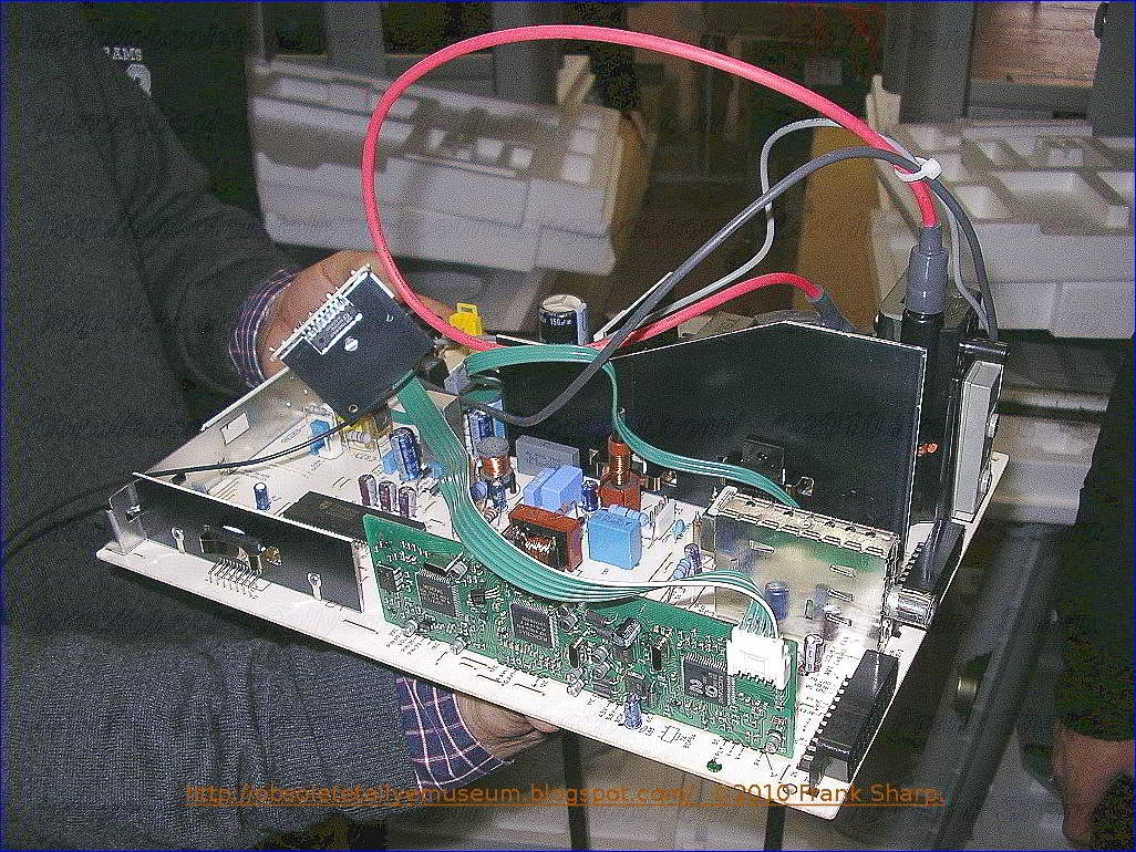
on the right side the TV chassis is located and on the left the power supply unit.
MIVAR 20M2 CHASSIS CS1069/1 PHILIPS TDA8843 I2C-bus controlled PAL/NTSC/SECAM TV processor:
GENERAL DESCRIPTION:
The various versions of the PHILIPS TDA 884X/5X series are

I2C-bus controlled single chip TV processors which are
intended to be applied in PAL, NTSC, PAL/NTSC and
multi-standard television receivers. The N2 version is pin
and application compatible with the N1 version, however,
a new feature has been added which makes the N2 more
attractive. The IF PLL demodulator has been replaced by
an alignment-free IF PLL demodulator with internal VCO
(no tuned circuit required). The setting of the various
frequencies (33.4, 33.9, 38, 38.9, 45,75 and 58.75 MHz)
can be made via the I2C-bus.
Because of this difference the N2 version is compatible
with the N1, however, N1 devices cannot be used in an
optimised N2 application.
Functionally the IC series is split up is 3 categories, viz:
· Versions intended to be used in economy TV receivers
with all basic functions (envelope: S-DIP 56 and QFP
64)
· Versions with additional features like E-W geometry
control, H-V zoom function and YUV interface which are
intended for TV receivers with 110° picture tubes
(envelope: S-DIP 56)
· Versions which have in addition a second RGB input
with saturation control and a second CVBS output
(envelope: QFP 64)
FUNCTIONAL DESCRIPTION
Vision IF amplifier
The IF-amplifier contains 3 ac-coupled control stages with
a total gain control range which is higher then 66 dB. The
sensitivity of the circuit is comparable with that of modern
IF-IC’s.
The video signal is demodulated by means of an
alignment-free PLL carrier regenerator with an internal
VCO. This VCO is calibrated by means of a digital control
circuit which uses the X-tal frequency of the colour
decoder as a reference. The frequency setting for the
various standards (33.4, 33.9, 38, 38.9, 45.75 and 58.75
MHz) is realised via the I2C-bus. To get a good
performance for phase modulated carrier signals the
control speed of the PLL can be increased by means of the
FFI bit.
The AFC output is generated by the digital control circuit of
the IF-PLL demodulator and can be read via the I2C-bus.
For fast search tuning systems the window of the AFC can
be increased with a factor 3. The setting is realised with the
AFW bit. The AFC data is valid only when the horizontal
PLL is in lock (SL = 1)
Depending on the type the AGC-detector operates on
top-sync level (single standard versions) or on top sync
and top white- level (multi standard versions). The
demodulation polarity is switched via the I2C-bus. The
AGC detector time-constant capacitor is connected
externally. This mainly because of the flexibility of the
application. The time-constant of the AGC system during
positive modulation is rather long to avoid visible variations
of the signal amplitude. To improve the speed of the AGC
system a circuit has been included which detects whether
the AGC detector is activated every frame period. When
during 3 field periods no action is detected the speed of the
system is increased. For signals without peak white
information the system switches automatically to a gated
black level AGC. Because a black level clamp pulse is
required for this way of operation the circuit will only switch
to black level AGC in the internal mode.
The circuits contain a video identification circuit which is
independent of the synchronisation circuit. Therefore
search tuning is possible when the display section of the
receiver is used as a monitor. However, this ident circuit
cannot be made as sensitive as the slower sync ident
circuit (SL) and we recommend to use both ident outputs
to obtain a reliable search system. The ident output is
supplied to the tuning system via the I2C-bus.
The input of the identification circuit is connected to pin 13
(S-DIP 56 devices), the “internal” CVBS input (see Fig.6).
This has the advantage that the ident circuit can also be
made operative when a scrambled signal is received
(descrambler connected between pin 6 (IF video output)
and pin 13). A second advantage is that the ident circuit
can be used when the IF amplifier is not used (e.g. with
built-in satellite tuners).
The video ident circuit can also be used to identify the
selected CBVS or Y/C signal. The switching between the
2 modes can be realised with the VIM bit.
Video switches
The circuits have two CVBS inputs (internal and external
CVBS) and a Y/C input. When the Y/C input is not required
the Y input can be used as third CVBS input. The switch
configuration is given in Fig.6. The selection of the various
sources is made via the I2C-bus.
For the TDA 884X devices the video switch configuration
is identical to the switch of the TDA8374/75 series. So the
circuit has one CVBS output (amplitude of 2 VP-P for the
TDA 884X series) and the I2C-bus control is similar to that
of the TDA 8374/75. For the TDA 885X IC’s the video
switch circuit has a second output (amplitude of 1 VP-P)
which can be set independently of the position of the first
output. The input signal for the decoder is also available on
the CVBS1-output.
Therefore this signal can be used to drive the Teletext
decoder. If S-VHS is selected for one of the outputs the
luminance and chrominance signals are added so that a
CVBS signal is obtained again.
Sound circuit
The sound bandpass and trap filters have to be connected
 externally. The filtered intercarrier signal is fed to a limiter
circuit and is demodulated by means of a PLL
demodulator. This PLL circuit tunes itself automatically to
the incoming carrier signal so that no adjustment is
required.
The volume is controlled via the I2C-bus. The deemphasis
capacitor has to be connected externally. The
non-controlled audio signal can be obtained from this pin
(via a buffer stage).
The FM demodulator can be muted via the I2C-bus. This
function can be used to switch-off the sound during a
channel change so that high output peaks are prevented.
The TDA 8840/41/42/46 contain an Automatic Volume
Levelling (AVL) circuit which automatically stabilises the
audio output signal to a certain level which can be set by
the viewer by means of the volume control. This function
prevents big audio output fluctuations due to variations of
the modulation depth of the transmitter. The AVL function
can be activated via the I2C-bus.
Synchronisation circuit
The sync separator is preceded by a controlled amplifier
which adjusts the sync pulse amplitude to a fixed level.
These pulses are fed to the slicing stage which is operating
at 50% of the amplitude. The separated sync pulses are
fed to the first phase detector and to the coincidence
detector. This coincidence detector is used to detect
whether the line oscillator is synchronised and can also be
used for transmitter identification. This circuit can be made
less sensitive by means of the STM bit. This mode can be
used during search tuning to avoid that the tuning system
will stop at very weak input signals. The first PLL has a
very high statical steepness so that the phase of the
picture is independent of the line frequency.
The horizontal output signal is generated by means of an
oscillator which is running at twice the line frequency. Its
frequency is divided by 2 to lock the first control loop to the
incoming signal. The time-constant of the loop can be
forced by the I2C-bus (fast or slow). If required the IC can
select the time-constant depending on the noise content of
the incoming video signal.
The free-running frequency of the oscillator is determined
by a digital control circuit which is locked to the reference
signal of the colour decoder. When the IC is switched-on
the horizontal output signal is suppressed and the
oscillator is calibrated as soon as all sub-address bytes
have been sent. When the frequency of the oscillator is
correct the horizontal drive signal is switched-on. To obtain
a smooth switching-on and switching-off behaviour of the
horizontal output stage the horizontal output frequency is
doubled during switch-on and switch-off (slow start/stop).
During that time the duty cycle of the output pulse has such
a value that maximum safety is obtained for the output
stage.
externally. The filtered intercarrier signal is fed to a limiter
circuit and is demodulated by means of a PLL
demodulator. This PLL circuit tunes itself automatically to
the incoming carrier signal so that no adjustment is
required.
The volume is controlled via the I2C-bus. The deemphasis
capacitor has to be connected externally. The
non-controlled audio signal can be obtained from this pin
(via a buffer stage).
The FM demodulator can be muted via the I2C-bus. This
function can be used to switch-off the sound during a
channel change so that high output peaks are prevented.
The TDA 8840/41/42/46 contain an Automatic Volume
Levelling (AVL) circuit which automatically stabilises the
audio output signal to a certain level which can be set by
the viewer by means of the volume control. This function
prevents big audio output fluctuations due to variations of
the modulation depth of the transmitter. The AVL function
can be activated via the I2C-bus.
Synchronisation circuit
The sync separator is preceded by a controlled amplifier
which adjusts the sync pulse amplitude to a fixed level.
These pulses are fed to the slicing stage which is operating
at 50% of the amplitude. The separated sync pulses are
fed to the first phase detector and to the coincidence
detector. This coincidence detector is used to detect
whether the line oscillator is synchronised and can also be
used for transmitter identification. This circuit can be made
less sensitive by means of the STM bit. This mode can be
used during search tuning to avoid that the tuning system
will stop at very weak input signals. The first PLL has a
very high statical steepness so that the phase of the
picture is independent of the line frequency.
The horizontal output signal is generated by means of an
oscillator which is running at twice the line frequency. Its
frequency is divided by 2 to lock the first control loop to the
incoming signal. The time-constant of the loop can be
forced by the I2C-bus (fast or slow). If required the IC can
select the time-constant depending on the noise content of
the incoming video signal.
The free-running frequency of the oscillator is determined
by a digital control circuit which is locked to the reference
signal of the colour decoder. When the IC is switched-on
the horizontal output signal is suppressed and the
oscillator is calibrated as soon as all sub-address bytes
have been sent. When the frequency of the oscillator is
correct the horizontal drive signal is switched-on. To obtain
a smooth switching-on and switching-off behaviour of the
horizontal output stage the horizontal output frequency is
doubled during switch-on and switch-off (slow start/stop).
During that time the duty cycle of the output pulse has such
a value that maximum safety is obtained for the output
stage.
 To protect the horizontal output transistor the horizontal
drive is immediately switched off when a power-on-reset is
detected. The drive signal is switched-on again when the
normal switch-on procedure is followed, i.e. all
sub-address bytes must be sent and after calibration the
horizontal drive signal will be released again via the slow
start procedure. When the coincidence detector indicates
an out-of-lock situation the calibration procedure is
repeated. The circuit has a second control loop to generate
the drive pulses for the horizontal driver stage. The
horizontal output is gated with the flyback pulse so that the
horizontal output transistor cannot be switched-on during
the flyback time.
To protect the horizontal output transistor the horizontal
drive is immediately switched off when a power-on-reset is
detected. The drive signal is switched-on again when the
normal switch-on procedure is followed, i.e. all
sub-address bytes must be sent and after calibration the
horizontal drive signal will be released again via the slow
start procedure. When the coincidence detector indicates
an out-of-lock situation the calibration procedure is
repeated. The circuit has a second control loop to generate
the drive pulses for the horizontal driver stage. The
horizontal output is gated with the flyback pulse so that the
horizontal output transistor cannot be switched-on during
the flyback time.
 Via the I2C-bus adjustments can be made of the horizontal
and vertical geometry. The vertical sawtooth generator
drives the vertical output drive circuit which has a
differential output current. For the E-W drive a single
ended current output is available. A special feature is the
zoom function for both the horizontal and vertical
deflection and the vertical scroll function which are
available in some versions. When the horizontal scan is
reduced to display 4:3 pictures on a 16:9 picture tube an
accurate video blanking can be switched on to obtain well
defined edges on the screen.
Overvoltage conditions (X-ray protection) can be detected
via the EHT tracking pin. When an overvoltage condition is
detected the horizontal output drive signal will be
switched-off via the slow stop procedure but it is also
possible that the drive is not switched-off and that just a
protection indication is given in the I2C-bus output byte.
The choice is made via the input bit PRD. The IC’s have a
second protection input on the j2 filter capacitor pin. When
this input is activated the drive signal is switched-off
immediately and switched-on again via the slow start
procedure. For this reason this protection input can be
used as “flash protection”.
The drive pulses for the vertical sawtooth generator are
obtained from a vertical countdown circuit. This countdown
circuit has various windows depending on the incoming
signal (50 Hz or 60 Hz and standard or non standard). The
countdown circuit can be forced in various modes by
means of the I2C-bus. During the insertion of RGB signals
the maximum vertical frequency is increased to 72 Hz so
that the circuit can also synchronise on signals with a
higher vertical frequency like VGA. To obtain short
switching times of the countdown circuit during a channel
change the divider can be forced in the search window by
means of the NCIN bit. The vertical deflection can be set
in the de-interlace mode via the I2C bus.
To avoid damage of the picture tube when the vertical
deflection fails the guard output current of the TDA
8350/51 can be supplied to the beam current limiting input.
When a failure is detected the RGB-outputs are blanked
and a bit is set (NDF) in the status byte of the I2C-bus.
When no vertical deflection output stage is connected this
guard circuit will also blank the output signals. This can be
overruled by means of the EVG bit.
Chroma and luminance processing
The circuits contain a chroma bandpass and trap circuit.
The filters are realised by means of gyrator circuits and
they are automatically calibrated by comparing the tuning
frequency with the X-tal frequency of the decoder. The
luminance delay line and the delay for the peaking circuit
are also realised by means of gyrator circuits. The centre
frequency of the chroma bandpass filter is switchable via
the I2C-bus so that the performance can be optimised for
“front-end” signals and external CVBS signals. During
SECAM reception the centre frequency of the chroma trap
is reduced to get a better suppression of the SECAM
carrier frequencies. All IC’s have a black stretcher circuit
which corrects the black level for incoming video signals
which have a deviation between the black level and the
blanking level (back porch). The timeconstant for the black
stretcher is realised internally.
The resolution of the peaking control DAC has been
increased to 6 bits. All IC’s have a defeatable coring
function in the peaking circuit. Some of these IC’s have a
YUV interface (see table on page 2) so that picture
improvement IC’s like the TDA 9170 (Contrast
improvement), TDA 9177 (Sharpness improvement) and
TDA 4556/66 (CTI) can be applied. When the CTI IC’s are
applied it is possible to increase the gain of the luminance
channel by means of the GAI bit in subaddress 03 so that
the resulting RGB output signals are not affected.
Colour decoder
Depending on the IC type the colour decoder can decode
PAL, PAL/NTSC or PAL/NTSC/SECAM signals. The
PAL/NTSC decoder contains an alignment-free X-tal
oscillator, a killer circuit and two colour difference
demodulators. The 90° phase shift for the reference signal
is made internally.
The IC’s contain an Automatic Colour Limiting (ACL)
circuit which is switchable via the I2C-bus and which
prevents that oversaturation occurs when signals with a
high chroma-to-burst ratio are received. The ACL circuit is
designed such that it only reduces the chroma signal and
not the burst signal. This has the advantage that the colour
sensitivity is not affected by this function.
The SECAM decoder contains an auto-calibrating PLL
demodulator which has two references, viz: the 4.4 MHz
sub-carrier frequency which is obtained from the X-tal
oscillator which is used to tune the PLL to the desired
free-running frequency and the bandgap reference to
obtain the correct absolute value of the output signal. The
VCO of the PLL is calibrated during each vertical blanking
period, when the IC is in search or SECAM mode.
The frequency of the active X-tal is fed to the Fsc output
(pin 33) and can be used to tune an external comb filter
(e.g. the SAA 4961).
The base-band delay line (TDA 4665 function) is
integrated in the PAL/SECAM IC’s and in the NTSC IC
TDA 8846A. In the latter IC it improves the cross colour
performance (chroma comb filter). The demodulated
colour difference signals are internally supplied to the
delay line. The colour difference matrix switches
automatically between PAL/SECAM and NTSC, however,
it is also possible to fix the matrix in the PAL standard.
The “blue stretch” circuit is intended to shift colour near
“white” with sufficient contrast values towards more blue to
obtain a brighter impression of the picture.
Which colour standard the IC’s can decode depends on
the external X-tals. The X-tal to be connected to pin 34
must have a frequency of 3.5 MHz (NTSC-M, PAL-M or
PAL-N) and pin 35 can handle X-tals with a frequency of
4.4 and 3.5 MHz. Because the X-tal frequency is used to
tune the line oscillator the value of the X-tal frequency
must be given to the IC via the I2C-bus. It is also possible
to use the IC in the so called “Tri-norma” mode for South
America. In that case one X-tal must be connected to pin
34 and the other 2 to pin 35. The switching between the 2
latter X-tals must be done externally. This has the
consequence that the search loop of the decoder must be
controlled by the m-computer. To prevent calibration
problems of the horizontal oscillator the external switching
between the 2 X-tals should be carried out when the
oscillator is forced to pin 34. For a reliable calibration of the
horizontal oscillator it is very important that the X-tal
indication bits (XA and XB) are not corrupted. For this
reason the X-tal bits can be read in the output bytes so that
the software can check the I2C-bus transmission.
RGB output circuit and black-current stabilisation
The colour-difference signals are matrixed with the
luminance signal to obtain the RGB-signals. The TDA
884X devices have one (linear) RGB input. This RGB
signal can be controlled on contrast and brightness (like
TDA 8374/75). By means of the IE1 bit the insertion
blanking can be switched on or off. Via the IN1 bit it can be
read whether the insertion pin has a high level or not.
The TDA 885X IC’s have an additional RGB input. This
RGB signal can be controlled on contrast, saturation and
brightness. The insertion blanking of this input can be
switched-off by means of the IE2 bit. Via the IN2 bit it can
be read whether the insertion pin has a high level or not.
The output signal has an amplitude of about 2 volts
black-to-white at nominal input signals and nominal
settings of the controls. To increase the flexibility of the IC
it is possible to insert OSD and/or teletext signals directly
at the RGB outputs. This insertion mode is controlled via
the insertion input (pin 26 in the S-DIP 56- and pin 38 in the
QFP-64 envelope). This blanking action at the RGB
outputs has some delay which must be compensated
externally.
Via the I2C-bus adjustments can be made of the horizontal
and vertical geometry. The vertical sawtooth generator
drives the vertical output drive circuit which has a
differential output current. For the E-W drive a single
ended current output is available. A special feature is the
zoom function for both the horizontal and vertical
deflection and the vertical scroll function which are
available in some versions. When the horizontal scan is
reduced to display 4:3 pictures on a 16:9 picture tube an
accurate video blanking can be switched on to obtain well
defined edges on the screen.
Overvoltage conditions (X-ray protection) can be detected
via the EHT tracking pin. When an overvoltage condition is
detected the horizontal output drive signal will be
switched-off via the slow stop procedure but it is also
possible that the drive is not switched-off and that just a
protection indication is given in the I2C-bus output byte.
The choice is made via the input bit PRD. The IC’s have a
second protection input on the j2 filter capacitor pin. When
this input is activated the drive signal is switched-off
immediately and switched-on again via the slow start
procedure. For this reason this protection input can be
used as “flash protection”.
The drive pulses for the vertical sawtooth generator are
obtained from a vertical countdown circuit. This countdown
circuit has various windows depending on the incoming
signal (50 Hz or 60 Hz and standard or non standard). The
countdown circuit can be forced in various modes by
means of the I2C-bus. During the insertion of RGB signals
the maximum vertical frequency is increased to 72 Hz so
that the circuit can also synchronise on signals with a
higher vertical frequency like VGA. To obtain short
switching times of the countdown circuit during a channel
change the divider can be forced in the search window by
means of the NCIN bit. The vertical deflection can be set
in the de-interlace mode via the I2C bus.
To avoid damage of the picture tube when the vertical
deflection fails the guard output current of the TDA
8350/51 can be supplied to the beam current limiting input.
When a failure is detected the RGB-outputs are blanked
and a bit is set (NDF) in the status byte of the I2C-bus.
When no vertical deflection output stage is connected this
guard circuit will also blank the output signals. This can be
overruled by means of the EVG bit.
Chroma and luminance processing
The circuits contain a chroma bandpass and trap circuit.
The filters are realised by means of gyrator circuits and
they are automatically calibrated by comparing the tuning
frequency with the X-tal frequency of the decoder. The
luminance delay line and the delay for the peaking circuit
are also realised by means of gyrator circuits. The centre
frequency of the chroma bandpass filter is switchable via
the I2C-bus so that the performance can be optimised for
“front-end” signals and external CVBS signals. During
SECAM reception the centre frequency of the chroma trap
is reduced to get a better suppression of the SECAM
carrier frequencies. All IC’s have a black stretcher circuit
which corrects the black level for incoming video signals
which have a deviation between the black level and the
blanking level (back porch). The timeconstant for the black
stretcher is realised internally.
The resolution of the peaking control DAC has been
increased to 6 bits. All IC’s have a defeatable coring
function in the peaking circuit. Some of these IC’s have a
YUV interface (see table on page 2) so that picture
improvement IC’s like the TDA 9170 (Contrast
improvement), TDA 9177 (Sharpness improvement) and
TDA 4556/66 (CTI) can be applied. When the CTI IC’s are
applied it is possible to increase the gain of the luminance
channel by means of the GAI bit in subaddress 03 so that
the resulting RGB output signals are not affected.
Colour decoder
Depending on the IC type the colour decoder can decode
PAL, PAL/NTSC or PAL/NTSC/SECAM signals. The
PAL/NTSC decoder contains an alignment-free X-tal
oscillator, a killer circuit and two colour difference
demodulators. The 90° phase shift for the reference signal
is made internally.
The IC’s contain an Automatic Colour Limiting (ACL)
circuit which is switchable via the I2C-bus and which
prevents that oversaturation occurs when signals with a
high chroma-to-burst ratio are received. The ACL circuit is
designed such that it only reduces the chroma signal and
not the burst signal. This has the advantage that the colour
sensitivity is not affected by this function.
The SECAM decoder contains an auto-calibrating PLL
demodulator which has two references, viz: the 4.4 MHz
sub-carrier frequency which is obtained from the X-tal
oscillator which is used to tune the PLL to the desired
free-running frequency and the bandgap reference to
obtain the correct absolute value of the output signal. The
VCO of the PLL is calibrated during each vertical blanking
period, when the IC is in search or SECAM mode.
The frequency of the active X-tal is fed to the Fsc output
(pin 33) and can be used to tune an external comb filter
(e.g. the SAA 4961).
The base-band delay line (TDA 4665 function) is
integrated in the PAL/SECAM IC’s and in the NTSC IC
TDA 8846A. In the latter IC it improves the cross colour
performance (chroma comb filter). The demodulated
colour difference signals are internally supplied to the
delay line. The colour difference matrix switches
automatically between PAL/SECAM and NTSC, however,
it is also possible to fix the matrix in the PAL standard.
The “blue stretch” circuit is intended to shift colour near
“white” with sufficient contrast values towards more blue to
obtain a brighter impression of the picture.
Which colour standard the IC’s can decode depends on
the external X-tals. The X-tal to be connected to pin 34
must have a frequency of 3.5 MHz (NTSC-M, PAL-M or
PAL-N) and pin 35 can handle X-tals with a frequency of
4.4 and 3.5 MHz. Because the X-tal frequency is used to
tune the line oscillator the value of the X-tal frequency
must be given to the IC via the I2C-bus. It is also possible
to use the IC in the so called “Tri-norma” mode for South
America. In that case one X-tal must be connected to pin
34 and the other 2 to pin 35. The switching between the 2
latter X-tals must be done externally. This has the
consequence that the search loop of the decoder must be
controlled by the m-computer. To prevent calibration
problems of the horizontal oscillator the external switching
between the 2 X-tals should be carried out when the
oscillator is forced to pin 34. For a reliable calibration of the
horizontal oscillator it is very important that the X-tal
indication bits (XA and XB) are not corrupted. For this
reason the X-tal bits can be read in the output bytes so that
the software can check the I2C-bus transmission.
RGB output circuit and black-current stabilisation
The colour-difference signals are matrixed with the
luminance signal to obtain the RGB-signals. The TDA
884X devices have one (linear) RGB input. This RGB
signal can be controlled on contrast and brightness (like
TDA 8374/75). By means of the IE1 bit the insertion
blanking can be switched on or off. Via the IN1 bit it can be
read whether the insertion pin has a high level or not.
The TDA 885X IC’s have an additional RGB input. This
RGB signal can be controlled on contrast, saturation and
brightness. The insertion blanking of this input can be
switched-off by means of the IE2 bit. Via the IN2 bit it can
be read whether the insertion pin has a high level or not.
The output signal has an amplitude of about 2 volts
black-to-white at nominal input signals and nominal
settings of the controls. To increase the flexibility of the IC
it is possible to insert OSD and/or teletext signals directly
at the RGB outputs. This insertion mode is controlled via
the insertion input (pin 26 in the S-DIP 56- and pin 38 in the
QFP-64 envelope). This blanking action at the RGB
outputs has some delay which must be compensated
externally.
 To obtain an accurate biasing of the picture tube a
“Continuous Cathode Calibration” circuit has been
developed. This function is realised by means of a 2-point
black level stabilisation circuit. By inserting 2 test levels for
each gun and comparing the resulting cathode currents
with 2 different reference currents the influence of the
picture tube parameters like the spread in cut-off voltage
can be eliminated. This 2-point stabilisation is based on
the principle that the ratio between the cathode currents is
coupled to the ratio between the drive voltages according
to:
The feedback loop makes the ratio between the cathode
currents Ik1 and Ik2 equal to the ratio between the
reference currents (which are internally fixed) by changing
the (black) level and the amplitude of the RGB output
signals via 2 converging loops. The system operates in
such a way that the black level of the drive signal is
controlled to the cut-off point of the gun so that a very good
grey scale tracking is obtained. The accuracy of the
adjustment of the black level is just dependent on the ratio
of internal currents and these can be made very accurately
in integrated circuits. An additional advantage of the
2-point measurement is that the control system makes the
absolute value of Ik1 and Ik2 identical to the internal
reference currents. Because this adjustment is obtained
by means of an adaption of the gain of the RGB control
stage this control stabilises the gain of the complete
channel (RGB output stage and cathode characteristic).
As a result variations in the gain figures during life will be
compensated by this 2-point loop.
An important property of the 2-point stabilisation is that the
off-set as well as the gain of the RGB path is adjusted by
the feedback loop. Hence the maximum drive voltage for
the cathode is fixed by the relation between the test
pulses, the reference current and the relative gain setting
of the 3 channels. This has the consequence that the drive
level of the CRT cannot be adjusted by adapting the gain
of the RGB output stage. Because different picture tubes
may require different drive levels the typical “cathode drive
level” amplitude can be adjusted by means of an I2C-bus
setting. Dependent on the chosen cathode drive level the
typical gain of the RGB output stages can be fixed taking
into account the drive capability of the RGB outputs (pins
19 to 21). More details about the design will be given in the
application report.
The measurement of the “high” and the “low” current of the
2- point stabilisation circuit is carried out in 2 consecutive
fields. The leakage current is measured in each field. The
maximum allowable leakage current is 100 mA
When the TV receiver is switched-on the RGB output
signals are blanked and the black current loop will try to set
the right picture tube bias levels. Via the AST bit a choice
can be made between automatic start-up or a start-up via
the m-processor. In the automatic mode the RGB drive
signals are switched-on as soon as the black current loop
has been stabilised. In the other mode the BCF bit is set to
0 when the loop is stabilised. The RGB drive can than be
switched-on by setting the AST bit to 0. In the latter mode
some delay can be introduced between the setting of the
BCF bit and the switching of the AST bit so that switch-on
effects can be suppressed.
It is also possible to start-up the devices with a fixed
internal delay (as with the TDA 837X and the TDA884X/5X
N1). This mode is activated with the BCO bit.
The vertical blanking is adapted to the incoming CVBS
signal (50 Hz or 60 Hz). When the flyback time of the
vertical output stage is longer than the 60 Hz blanking time
the blanking can be increased to the same value as that of
the 50 Hz blanking. This can be set by means of the LBM
bit.
For an easy (manual) adjustment of the Vg2 control voltage
the VSD bit is available. When this bit is activated the black
current loop is switched-off, a fixed black level is inserted
at the RGB outputs and the vertical scan is switched-off so
that a horizontal line is displayed on the screen. This line
can be used as indicator for the Vg2 adjustment. Because
of the different requirements for the optimum cut-off
voltage of the picture tube the RGB output level is
adjustable when the VSD bit is activated. The control
range is 2.5 ± 0.7 V and can be controlled via the
brightness control DAC.
It is possible to insert a so called “blue back” back-ground
level when no video is available. This feature can be
activated via the BB bit in the control2 subaddress.
MIVAR 20M2 CHASSIS CS1069/1 PHILIPS TDA8356 DC-coupled vertical deflection circuit:
To obtain an accurate biasing of the picture tube a
“Continuous Cathode Calibration” circuit has been
developed. This function is realised by means of a 2-point
black level stabilisation circuit. By inserting 2 test levels for
each gun and comparing the resulting cathode currents
with 2 different reference currents the influence of the
picture tube parameters like the spread in cut-off voltage
can be eliminated. This 2-point stabilisation is based on
the principle that the ratio between the cathode currents is
coupled to the ratio between the drive voltages according
to:
The feedback loop makes the ratio between the cathode
currents Ik1 and Ik2 equal to the ratio between the
reference currents (which are internally fixed) by changing
the (black) level and the amplitude of the RGB output
signals via 2 converging loops. The system operates in
such a way that the black level of the drive signal is
controlled to the cut-off point of the gun so that a very good
grey scale tracking is obtained. The accuracy of the
adjustment of the black level is just dependent on the ratio
of internal currents and these can be made very accurately
in integrated circuits. An additional advantage of the
2-point measurement is that the control system makes the
absolute value of Ik1 and Ik2 identical to the internal
reference currents. Because this adjustment is obtained
by means of an adaption of the gain of the RGB control
stage this control stabilises the gain of the complete
channel (RGB output stage and cathode characteristic).
As a result variations in the gain figures during life will be
compensated by this 2-point loop.
An important property of the 2-point stabilisation is that the
off-set as well as the gain of the RGB path is adjusted by
the feedback loop. Hence the maximum drive voltage for
the cathode is fixed by the relation between the test
pulses, the reference current and the relative gain setting
of the 3 channels. This has the consequence that the drive
level of the CRT cannot be adjusted by adapting the gain
of the RGB output stage. Because different picture tubes
may require different drive levels the typical “cathode drive
level” amplitude can be adjusted by means of an I2C-bus
setting. Dependent on the chosen cathode drive level the
typical gain of the RGB output stages can be fixed taking
into account the drive capability of the RGB outputs (pins
19 to 21). More details about the design will be given in the
application report.
The measurement of the “high” and the “low” current of the
2- point stabilisation circuit is carried out in 2 consecutive
fields. The leakage current is measured in each field. The
maximum allowable leakage current is 100 mA
When the TV receiver is switched-on the RGB output
signals are blanked and the black current loop will try to set
the right picture tube bias levels. Via the AST bit a choice
can be made between automatic start-up or a start-up via
the m-processor. In the automatic mode the RGB drive
signals are switched-on as soon as the black current loop
has been stabilised. In the other mode the BCF bit is set to
0 when the loop is stabilised. The RGB drive can than be
switched-on by setting the AST bit to 0. In the latter mode
some delay can be introduced between the setting of the
BCF bit and the switching of the AST bit so that switch-on
effects can be suppressed.
It is also possible to start-up the devices with a fixed
internal delay (as with the TDA 837X and the TDA884X/5X
N1). This mode is activated with the BCO bit.
The vertical blanking is adapted to the incoming CVBS
signal (50 Hz or 60 Hz). When the flyback time of the
vertical output stage is longer than the 60 Hz blanking time
the blanking can be increased to the same value as that of
the 50 Hz blanking. This can be set by means of the LBM
bit.
For an easy (manual) adjustment of the Vg2 control voltage
the VSD bit is available. When this bit is activated the black
current loop is switched-off, a fixed black level is inserted
at the RGB outputs and the vertical scan is switched-off so
that a horizontal line is displayed on the screen. This line
can be used as indicator for the Vg2 adjustment. Because
of the different requirements for the optimum cut-off
voltage of the picture tube the RGB output level is
adjustable when the VSD bit is activated. The control
range is 2.5 ± 0.7 V and can be controlled via the
brightness control DAC.
It is possible to insert a so called “blue back” back-ground
level when no video is available. This feature can be
activated via the BB bit in the control2 subaddress.
MIVAR 20M2 CHASSIS CS1069/1 PHILIPS TDA8356 DC-coupled vertical deflection circuit:
GENERAL DESCRIPTION
The TDA8356 is a power circuit for use in 90° and 110°
colour deflection systems for field frequencies of 50 to
120 Hz. The circuit provides a DC driven

vertical deflection
output circuit, operating as a highly efficient class G
system.
FEATURES
• Few external components
• Highly efficient fully DC-coupled vertical output bridge
circuit
• Vertical flyback switch
• Guard circuit
• Protection against:
– short-circuit of the output pins (7 and 4)
– short-circuit of the output pins to VP
• Temperature (thermal) protection
• High EMC immunity because of common mode inputs
• A guard signal in zoom mode.
FUNCTIONAL DESCRIPTION
The vertical driver circuit is a bridge configuration. The
deflection coil is connected between the output amplifiers,
which are driven in phase opposition. An external resistor
(RM) connected in series with the deflection coil provides
internal feedback information. The differential input circuit
is voltage driven. The input circuit has been adapted to
enable it to be used with the TDA9150, TDA9151B,
TDA9160A, TDA9162, TDA8366 and TDA8376 which
deliver symmetrical current signals. An external resistor
(RCON) connected between the differential input
determines the output current through the deflection coil.
The relationship between the differential input current and
the output current is defined by: Idiff × RCON = Icoil × RM.
The output current is adjustable from 0.5 A (p-p) to
2 A (p-p) by varying RM. The maximum input differential
voltage is 1.8 V. In the application it is recommended that
Vdiff = 1.5 V (typ). This is recommended because of the
spread of input current and the spread in the value of
RCON.
The flyback voltage is determined by an additional supply
voltage VFB. The principle of operatin
g with two supply
voltages (class G) makes it possible to fix the supply
voltage VP optimum for the scan voltage and the second
supply voltage VFB optimum for the flyback voltage. Using
this method, very high efficiency is achieved.
The supply voltage VFB is almost totally available as
flyback voltage across the coil, this being possible due to
the absence of a decoupling capacitor (not necessary, due
to the bridge configuration). The output circuit is fully
protected against the following:
• thermal protection
• short-circuit protection of the output pins (pins 4 and 7)
• short-circuit of the output pins to VP.
A guard circuit VO(guard) is provided. The guard circuit is
activated at the following conditions:
• during flyback
• during short-circuit of the coil and during short-circuit of
the output pins (pins 4 and 7) to VP or ground
• during open loop
• when the thermal protection is activated.
This signal can be used for blanking the picture tube
screen.
MIVAR 20M2 CHASSIS CS1069/1
90° TVTEXT 8-Bit Microcontroller, ROM-Versions: SDA5254:
1
General Descr
iption
The SDA 525x contains a slicer for TTX, VPS and WSS, an accelerating acquisition
hardware modul, a display generator for “Level 1” TTX data and an 8 bit microcontroller
running at 333 ns cycle time. The controller with dedicated hardware guarantees
flexibility, does most of the internal processing of TTX acquisition, transfers data to/from
the external memory interface and receives/transmits data via
I
2
C and UART user
interfaces. The block diagram shows the internal organization of the SDA 525x. The
Slicer combined with dedicated hardware stores TTX data in a VBI buffer of 1 Kbyte. The
microcontroller firmware does the total acquisition task (hamming- and parity-checks,
page search and evaluation of header control bits) once per field.
2
Features
Acquisition
• Feature selection via special function register
• Simultaneous reception of TTX, VPS and WSS
• Fixed framing code for VPS and TTX
• Acquisition during VBI
• Direct access to VBI RAM buffer
• Acquisition of packets X/26, X/27, 8/30 (firmware)
• Assistance of all relevant checks (firmware)
• 1-bit framing code error tolerance (switchable)
Display
• Features selectable via special function register
• 50/60 Hz display
• Level 1 serial attribute display pages
• Blanking and contrast reduction output
• 8 direct addressable display pages for SDA 5250, SDA 5254 and SDA 5255
• 1 direct addressable display page for SDA 5251 and SDA 5252
• 12
×
10 character matrix
• 96 character ROM (standard G0 character set)
• 143 national option characters for 11 languages
• 288 characters for X/26 display
• 6
4 block mosaic graphic characters
• 32 characters for OSD in expanded character ROM + 32 characters inside OSD box
• Conceal/reveal
• Transparent foreground/background - inside/outside of a box
• Contrast reduction inside/outside of a box
• Cursor (colour changes from foreground to background colour)
• Flash (flash rate 1s).
• Programmable horizontal and vertical sync delay
• Full screen background colour in outer screen
• Double size / double width / double height characters
Synchronization
• Display synchronization to sandcastle or Horizontal Sync (HS) and Vertical Sync (VS)
with start-stop-oscillator
• Independent clock systems for acquisition, display and controller
Microcontroller
• 8 bit C500-CPU (8051 compatible)
• 18 MHz internal clock
• 0.33
µ
s instruction cycle
• Parallel 8-bit data and 16...19 - bit address bus (ROMless-Version)
• Eight 16-bit data pointer registers (DPTR)
• Two 16-bit timers
• Watchdog timer
• Capture compare timer for infrared remote control decoding
• Serial interface (UART)
• 256 bytes on-chip RAM
• 8 Kbyte on-chip display-RAM (access via MOVX) for SDA 5250
, SDA 5254 and
SDA 5255
• 1 Kbyte on-chip display-RAM (access via MOVX) for SDA 5251 and SDA 5252
• 1 Kbyte on-chip TVT/VPS-Acquisition-buffer-RAM (access via MOVX)
• 1 Kbyte on-chip extended-RAM (access via MOVX) for SDA 5250, SDA 5254 and
SDA 5255
• 6 channel 8-bit pulse width modulation unit
• 2 channel 14-bit pulse width modulation unit
• 4 multiplexed ADC inputs with 8-bit resolution
• One 8-bit I/O port with open drain output and optional
I
2
C-Bus emulation (PORT 0)
• Two 8-bit multifunctional I/O ports (PORT 1, PORT 3)
• One 4-bit port working as digital or analog inputs (PORT 2)
• One 2-bit I/O port with optional functions
• One 3-bit I/O port with optional RAM/ROM address expansion up to 512 Kbyte
(ROMless-Version).
Display Generator
The display features of SDA525x are similar to the Siemens SDA5248 TTX controller.
The display generator reads character addresses and control characters from the
display memory, selects the pixel information from the character ROM and translates it
into RGB values corresponding to the World Standard Teletext
Norm. The national
option character bits for 11 languages inclusive X/26 characters are also supported.
6.2.1
Display Format and Timing
A page consists of 25 rows of 40 characters each. One character covers a matrix of
12 horizontal and 10 vertical pixels. The pixel frequency should be 12 MHz
corresponding to 1 µs for one character and 40 µs for one row. A total of 250 TV lines
are used for TTX display. The display can be shifted horizontally from 0 µs to 21.33 µs
with respect to HS and vertically from line 1 (314) to line 64 (377) with respect to VS. The
display position is determined by the registers DHD and DVD.
Note: To avoid interferences between the subharmonics of the 18 MHz controller clock
and the 12 MHz pixel clock, a pixel clock of about 11,5 MHz is recommended.
6.2.2
Display Cursor
A cursor is available which changes foreground to background colour for one character.
Cursor flash can be realized via software enabling/disabling the cursor. The cursor
position is defined by cursor position registers DCRP and DCCP.
6.2.3
Flash
A character background flash (character is changed to background colour) is realized by
hardware. The flash frequency is 1 Hz with a duty cycle of 32:18.
6.2.4
Full Screen Background Colour
The SDA 525x delivers the new full screen background colour feature. Special function
register SFR DTIM(7-5) includes three bits which define the default background colour
for the inner and outer screen area.
6.2.5
Clear Page Logic
The clear page logic generates a signal which is interpreted by the character generator
to identify non displayable rows. In row 25 specific information is stored by the
microcontroller indicating which of the rows 0 - 24 should be interpreted as erased during
character generation. At the beginning of each row the special control characters are
read from the display memory.
Microcontroller
6.3.1
Architecture
The CPU manipulates operands in two memory spaces: the program memory space,
and the data memory space. The program memory address space is provided to
accommodate relocatable code.
The data memory address space is divided into the 256-byte internal data RAM, XRAM
(extended data memory, accessible with MOVX-instructions) and the 128-byte Special
Function Register (SFR) address spaces. Four register banks (each bank has eight
registers), 128 addressable bits, and the stack reside in the internal data RAM. The stack
depth is limited only by the available internal data RAM. It’s location is determined by the
8-bit stack pointer. All registers except the program counter and the four 8-register banks
reside in the special function register address space. These memory map

ped registers
include arithmetic registers, pointers, I/O-ports, registers for the interrupt system, timers,
pulse width modulator and serial channel. Many locations in the SFR-address space are
addressable as bits.
Note that reading from unused locations within data memory will yield undefined data.
Conditional branches are performed relative to the 16 bit program counter. The register-
indirect jump permits branching relative to a 16-bit base register with an offset provided
by an 8-bit index register. Sixteen-bit jumps and calls permit branching to any location in
the memory address space.
The processor as five methods for addressing source operands: register, direct, register-
indirect, immediate, and base-register plus index-register indirect addressing.
The first three methods can be used for addressing destination operands. Most
instructions have a “destination, source” field that specifies the data type, addressing
methods and operands involved. For operations other than moves, the destination
operand is also a source operand.
Registers in the four 8-register banks can be accessed through register, direct, or
register-indirect addressing; the lower 128 bytes of internal data RAM through direct or
register-indirect addressing, the upper 128 bytes of internal data RAM through register-
indirect addressing; and the special function registers through direct addressing. Look-
up tables resident in program memory can be accessed through base-register plus
index-register indirect addressing.
CPU-Hardware
Instruction Decoder
Each program instruction is decoded by the instruction decoder. This unit generates the
internal signals that control the functions of each unit within the CPU-section. These
signals control the sources and destination of data, as well as the function of the
Arithmetic/Logic Unit (ALU).
Program Control Section
The program control section controls the sequence in which the instructions stored in
program memory are executed. The conditional branch logic enables conditions internal
and external to the processor to cause a change in the sequence of program execution.
The 16-bit program counter holds the address of the instruction to be executed. It is
manipulated with the control transfer instructions listed in Chapter “Instruction Set” on
page 116.
Internal Data RAM
The internal data RAM provides a 256-byte scratch pad memory, which includes four
register banks and 128 direct addressable software flags. Each register bank contains
registers R0 – R7. The addressable flags are located in the 16-byte locations starting at
byte address 32 and ending with byte location 47 of the RAM-address space.
In addition to this standard internal data RAM the processor contains an extended
internal RAM. It can be considered as a part of an external data memory. It is referenced
by MOVX-instructions (MOVX A, @DPTR), the memory map is shown in Figure 21.
Arithmetic/Logic Unit (ALU)
The arithmetic section of the processor performs many data manipulation functions and
includes the Arithmetic/Logic Unit (ALU) and the A, B and PSW-registers. The ALU
accepts 8-bit data words from one or two sources and generates an 8-bit result under
the control of the instruction decoder. The ALU performs the arithmetic operations of
add, subtract, multiply, divide, increment, decrement, BCD-decimal-add-adjust and
compare, and the logic operations of and, or, exclusive-or, complement and rotate (right,
left, or nibble swap).
The A-register is the accumulator, the B-register is dedicated during multiply and divide
and serves as both a source and a destination. During all other operations the B-register
is simply another location of the special function register space and may be used for any
purpose.
 MIVAR 20M2 CHASSIS CS1069/1 TEA2261 SWITCH MODE POWER SUPPLY CONTROLLER: MIVAR CS1049 SWITCH 90°.
SUPPLY is based on TEA2261 (THOMSON) SMPS Design.
The control means IP1 provide a soft start for a safe start-up after
switching on the line power. This is accomplished via a resistor R5
charging slowly a capacitor C14 with a high capacitance which provides
the necessary power for the integrated circuit IP1 at pins 15 and 16.
Additionally
the SMPS starts with a low oscillating frequency to avoid a current
build-up in the switching transistor T1. A current build-up can arise
when the energy stored in the primary inductance is not fully
transferred to the secondary side before a new conduction period is
initiated. This will lead to operation in continuous mode and the
switching transistor T1 may leave therefore his safe operating area. To
reduce the oscillating frequency during start-up, the SMPS includes a
resistor R511 and a diode D9 in series which connect the capacitor C26
with a capacitor C12 which is charged by the feed-back winding W2. The
capacitor C12 is not charged up initially when the SMPS is switched on.
Therefore, the diode D9 disconnects capacitor C26 from capacitor C12.
The operating frequency is then fixed by R13 and C26, which is a low
frequency (a few kHz). After a certain time capacitor C12 is charged up
and then D9 will be conducting and an additional current will charge C26
via R511, thus the oscillating frequency increases to its normal
operating frequency (about 22 kHz). This ensures that the SMPS starts
safely in discontinuous mode, i.e. the energy stored in the primary
inductance is always fully transferred to the secondary side before a
new conduction period of transistor T1 is initiated.
The start-up
of this known SMPS is depending on the charge-up time of capacitor C14
via resistor R5, therefore, depending on the voltage value of the AC
mains input voltage. This leads to a quite long start-up time at a low
mains input voltage.
The invention relates to a switch mode power supply (SMPS) comprising
control means which include an oscillator for generating a pulse width
modulated signal.
It is the object of the invention to provide a SMPS as previously
described having a fast start-up time over a wide input voltage range.
This object is accomplished with a switch mode power supply according to
claim 1. The subclaims relate to preferred embodiments.
According
to the invention, the switch mode power supply comprises a network
which provides in case of a high input voltage a start-up with a low
oscillation frequency only for the start-up time. After start-up, the
oscillation frequency changes to the normal oscillating frequency. In
case of a low input voltage, the network provides a start-up with
essentially the normal oscillation frequency. This can be done without
safety risk for the switching transistor because the operating voltages
are low in this case. Even if a slight current build-up phenomenon
occurs during start-up, the switching transistor stays in the safe
operating area because of the low voltages. The network, therefore,
includes means which change the oscillating frequency only in case of a
high mains input voltage. No soft start is provided in case of a low
mains input voltage. The frequency control of the oscillation frequency
can be done advantageously by frequency control means including a
transistor stage which change in case of a high mains input voltage the
time constant of the oscillator network which determines the oscillation
frequency.
In a special embodiment the network comprises a
transistor used in inverse mode as a switching element. With this
circuit arrangement an additional diode is not necessary. This utilizes
the fact that the maximum collector base breakdown's voltage is
distinctly higher than the maximum emitter base breakdown's voltage. The
SMPS can be used especially for a TV receiver which works in a mains
input voltage range of 90 V to 270 V, in a TV receiver the start-up time
of the picture tube has to be considered additionally.

.POSITIVE AND NEGATIVE CURRENT UP TO
1.2A and – 2A
.LOW START-UP CURRENT
.DIRECT DRIVE OF THE POWER TRANSISTOR
.TWO LEVELS TRANSISTOR CURRENT LIMITATION
.DOUBLE PULSE SUPPRESSION
.SOFT-STARTING
.UNDER AND OVERVOLTAGE LOCK-OUT
.AUTOMATIC STAND-BY MODE RECOGNITION
.LARGE POWER RANGE CAPABILITY IN
STAND-BY (Burst mode)
.INTERNAL PWM SIGNAL GENERATOR
DESCRIPTION
The TEA2260/61 is a monolithic integrated circuit
for the use in primary part of an off-line switching
mode power supply.
All functions required for SMPS control under normal
operating,transient or abnormal conditions are
provided.
The capability of working according to the ”masterslave”
concept, or according to the ”primary regulation”
mode makes the TEA2260/61 very flexible
and easy to use. This is particularly true for TV
receivers where the IC provides an attractive and
low cost solution (no need of stand-by auxiliary
power supply).
GENERAL DESCRIPTION

The TEA2260/61 is an off-line switch mode power
supply controller. The synchronization functionand
the specificoperationin stand-bymodemake itwell
adapted to video applications such as TV sets,
VCRs, monitors, etc...
The TEA2260/61 can be used in two types of
architectures :
- Master/slave architecture. In this case, the
TEA2260/61 drives the power transistor according
to the pulse width modulated signals generated
by the secondary located master circuit. A
pulse transformer provides the feedback (see
Figure 1).
- Conventional architecture with linear feedback
signal (feedback sources : optocoupler or transformer
winding) (see Figure 2).
Using the TEA2260/61, the stand-by auxiliary
power supply, often realized with a small but costly
50Hz transformer, is no longer necessary. The
burst mode operation of the TEA2260/61 makes
possible the control of very low output power (down
to less than 1W) with the main power transformer.
When used in a master/slave architecture, the
TEA2260/61and also the power transistor turn-off
can be easily synchronized with the line transformer.
The switching noise cannot disturb the
picture in this case.
As an S.M.P.S.controller, the TEA2260/61features
the following functions :
- Power supply start-up (with soft-start)
- PWM generator
- Direct power transistor drive (+1.2A, -2.0A)
- Safety functions : pulse by pulse current limitation,
output power limitation, over and under voltage
lock-out.
S.M.P.S. OPERATING DESCRIPTION
Starting Mode - Stand By Mode
Power for circuit supply is taken from the mains
through a high value resistor before starting. As
long as VCC of the TEA2260/61 is below VCC start,
the quiescent current is very low (typically 0.7mA)
and the electrolytic capacitor across VCC is linearly
charged. When VCC reaches VCC start (typically
10.3V), the circuit starts, generating output pulses
with a soft-starting. Then the SMPS goes into the
stand-bymode and the output voltage is a percentage
of the nominal output voltage (eg. 80%).
For this the TEA2260/61 contains all the functions
required for primary mode regulation : a fixed frequency
oscillator, a voltage reference, an error
amplifier and a pulse width modulator (PWM).
For transmission of low power with a good efficiency
in stand-by, an automatic burst generation
system is used, in order to avoid audible noise.
Normal Mode (secondary regulation)
The normal operating of the TV set is obtained by
sending to the TEA2260/61regulation pulses generated
by a regulator located in the secondary side
of the power supply.
This architectureuses the ”Master-slave Concept”,
advantages of which are now well-known especially
the very high efficiency in stand-bymode, and
the accurate regulation in normal mode.
Stand-by mode or normal mode are obtained by
supplying or not the secondary regulator. This can
be ordonneredfor exemple by a microprocessor in
relation with the remote control unit.
Regulation pulses are applied to the TEA2260/61
through a small pulse-transformer to the IN input
(Pin 2). This input is sensitive to positive square
pulses. The typical threshold of this input is 0.85V.
The frequency of pulses coming from the secondary
regulator can be lower or higher than the
frequency of the starting oscillator.
The TEA2260/61has no soft-starting system when
it receives pulses from the secondary. The softstarting
has to be located in the secondary regulator.
Due to the principle of the primary regulation,
pulses generated by the starting system automatically
disappear when the voltage delivered by the
SMPS increases.
Stand-by Mode - Normal Mode Transition
During the transition there are simultaneously
pulses coming from the primary and secondary
regulators.
These signals are not synchronizedand some care
has to betaken toensure the safety of theswitching
power transistor.
Avery sure and simple way consist in checking the
transformer demagnetization state.
- A primary pulse is taken in account only if the
transformer is demagnetized after a conduction
of the power transistor required by the secondary
regulator.
- A secondary pulse is taken in account only if the
transformer is demagnetized after a conduction
of the power transistor required by the primary
regulator.
With this arrangement the switching safety area of
the power transistor is respected and there is no
risk of transformer magnetization.
The magnetization state of the transformer is
checked by sensing the voltage across a winding
of the transformer (generally the same which supplies
the TEA2261). This is made by connecting a
resistor between this winding and the demagnetization
sensing input of the circuit (Pin 1).
SECURITY FUNCTIONS OF THE TEA2261 (see flow-chart below)
- Undervoltage detection. This protection works
in association with the starting device ”VCC
switch” (see paragraph Starting-mode - standby
mode). If VCC is lower than VCCstop (typically
7.4V) output pulses are inhibited, in order to avoid
wrong operation of the power supply or bad
power transistor drive.
- Overvoltage detection. If VCC exceedsVCCmax
(typically 15.7V) output pulses are inhibited. Restarting
of the power supply is obtained by reducing
VCC below VCCstop.
- Current limitation of the power transistor. The
current is measured by a shunt resistor. Adouble
threshold system is used :
- When the first threshold (VIM1) is reached, the
conduction of the power transistor is stopped
until the end of the period : a new conduction
signal is needed to obtain conduction again.
- Furthermore as long as the first threshold is
reached (it means during several periods), an
external capacitor C2 is charged. When the
voltage across the capacitor reaches VC2 (typically
2.55V) the output is inhibited.This is called
the ”repetitive overload protection”. If the overload
diseappears before VC2 is reached, C2 is
discharged, so transient overloads are tolerated.
- Second current limitation threshold (VIM2).
When this thresholdis reached the output of the
circuit is immediatly inhibited. This protection is
helpfull in case of hard overload for example to
avoid the magnetization of the transformer.
- Restart of the power supply. After stopping due
to VC2, VIM2, VCCMax or VCCstop triggering, restart
of the power supply can be obtained by the
normal operating of the ”VCC switch” but thanks
to an integrted counter, if normal restart cannot
be obtained after three trials, the circuit is definitively
stopped. In this case it is necessary to
reduce VCC below approximately 5V to reset the
circuit. From a practical point of view, it means
that the power supply has to be temporarily disconnected
from any power source to get the
restart.


A SCART Connector (which stands for Syndicat des Constructeurs d'Appareils Radiorécepteurs et Téléviseurs) is a standard for connecting audio-visual equipment together. The official standard for SCART is CENELEC document number EN 50049-1. SCART is also known as Péritel (especially in France) and Euroconnector but the name SCART will be used exclusively herein. The standard defines a 21-pin connector (herein after a SCART connector) for carrying analog television signals. Various pieces of equipment may be connected by cables having a plug fitting the SCART connectors. Television apparatuses commonly include one or more SCART connectors.
Although a SCART connector is bidirectional, the present invention is concerned with the use of a SCART connector as an input connector for receiving signals into a television apparatus. A SCART connector can receive input television signals either in an RGB format in which the red, green and blue signals are received on Pins 15, 11 and 7, respectively, or alternatively in an S-Video format in which the luminance (Y) and chroma (C) signals are received on Pins 20 and 15. As a result of the common usage of Pin 15 in accordance with the SCART standard, a SCART connector cannot receive input television signals in an RGB format and in an S-Video format at the same time.This kind of connector is todays obsoleted !Consequently many commercially available television apparatuses include a separate SCART connectors each dedicated to receive input television signals in one of an RGB format and an S-Video format. This limits the functionality of the SCART connectors. In practical terms, the number of SCART connectors which can be provided on a television apparatus is limited by cost and space considerations. However, different users wish the input a wide range of different combinations of formats of television signals, depending on the equipment they personally own and use. However, the provision of SCART connectors dedicated to input television signals in one of an RGB format and an S-Video format limits the overall connectivity of the television apparatus. Furthermore, for many users the different RGB format and S-Video format are confusing. Some users may not understand or may mistake the format of a television signal being supplied on a given cable from a given piece of equipment. This can result in the supply of input television signals of an inappropriate format for the SCART connector concerned.


 Founded in 1945 by Mr. Carlo Vichi class of 1923, The activity started in 1945 - in Milano, Via Ugo Tommei 5 street with fab
 rication of little radio apparates.


