The NORDMENDE SPECTRA COLOR L2UT CHASSIS FFS 772.535.A 772.536.A (4.570.D) was first tv color chassis from NORDMENDE sporting a 110° degree A66-140X CRT TUBE.
It's an hybrifd chassis with semiconductors and tubes.
The Tubes are used in Line deflection and frame deflection and horizontal oscillator too.
All other part are based on sophisticated - complex discretes circuits.
The chassis features ultrasonic remote control.
Was first NORDMENDE TV COLOR CHASSIS featuring a EHT Multiplier unit.
NORDMENDE SPECTRA COLOR L2UT CHASSIS FFS 772.535.A 772.536.A (4.570.D) power supply CONSTANT-VOLTAGE CONVERTER EMPLOYING THYRISTOR:

A
constant voltage converter having a rectifier for rectifying AC
power and with a thyristor connected between the rectifier and a
filter for selectively passing therethrough a rectified output to an
output terminal. There is a wave generator connected to the output
of the rectifier for producing a first signal and an intergrator
circuit connected to the output of the wave generator for producing
an integral output in response to this first signal. In addition
there is a detector circuit for detecting a fluctuation of the
rectified output power and for producing second signal. A comparison
circuit is connected between the intergrator circuit and the
detector circuit for producing third signal in accordance with the
comparison. A trigger circuit is connected between the comparison
circuit and the control gate of the thyristor for supplying a phase
control signal to the thyristor to thereby obtain a constant voltage
output regardless of the fluctuation of the rectified output.


1.
A constant voltage converter comprising an input of a power supply
means, an output terminal, filter means, rectifier means connected
to said input for rectifying a.c. power and for supplying output
thereof to said output terminal, thyristor means connected between
said rectifier means and said filter means for selectively passing
therethrough a rectified output to the output terminal by way of said
filter means, saw-tooth wave generator means connected between the
output of said rectifier means and at least one integrator circuit
means for producing an integral output in response to a saw-tooth wave
produced, a first transistor in said saw-tooth wave generator, the
input of said integrator circuit means being connected to a
collector of said first transistor, detector circuit means connected
to said output terminal for detecting a fluctuation of the
rectified output power and for producing an output signal, said
detector circuit means having a second transistor, pulse generator
circuit means connected between said saw-tooth wave generator means
and said detector circuit means for producing a trigger pulse to
said thyristor through a trigger means, a third transistor in said
pulse circuit generator means, the base of said third transistor
being connected to the output of said integrator circuit means, the
emitter thereof being connected to the emitter of said second
transistor in said detector circuit means, and the collector thereof
being connected to the gate of the thyristor means so as to supply a
phase control signal thereto, thereby obtaining a constant voltage
output regardless of the fluctuation of the rectified output.
Description:
This
invention relates to constant-voltage converters and more
particularly to a constant-voltage converter employing a thyristor.
Conventional
constant-voltage converters of the type employing a thyristor are
arranged to phase shift and full-wave-rectify an input a.c. power
applied thereto and to maintain the output voltages constant by
regulating the firing angle of the thyristor in comparison of the
output voltages with the phase-shifted and rectified input a.c.
power. When, however, these converters are connected to a common
a.c. source having a relatively high internal impedance, the
waveform of the phase-shifted and rectified a.c. input power is
distorted thereby causing undesired operations of the converters.
It
is therefore an object of the present invention to provide a
constant-voltage converter which correctly operates notwithstanding
the distortion of the input a.c. voltage.
Another
object of the invention is to provide a constant-voltage converter
which effectively suppress an undesired rush current.
Another
object of the invention is to provide a constant-voltage converter
having an improved feed-back circuit of a substantially constant
loop gain .
In the drawings:
FIG. 1 is a schematic view of a converter according to the present invention;
FIG. 2 is a diagram showing a circuit arrangement of the converter of FIG. 1;
FIG. 3 is a diagram showing various waveforms of signals appearing in the circuit of FIG. 2;
FIG.
4 is a diagram showing various waveforms appearing in the circuit
of FIG. 2 when an a.c. power is supplied to the circuit;
FIG. 5 is a diagram showing another circuit arrangement of the converter of FIG. 1;
FIG. 6 is a diagram showing waveforms of signals appearing in the circuit of FIG. 5; and
FIG. 7 is a diagram showing further another circuit arrangement of generator the of FIG. 1.
Referring now to FIG. 1, a cons

tant-voltage
converter 10 according to the present invention comprises a
rectifier 11 having two input terminals 12 and 13 through which an
a.c. power is supplied. The rectifier 11 is preferably a full-wave
rectifier although a half-wave rectifier may be employed. An output
14 of the rectifier 11 is connected through a line 15 to an anode of a
thyristor 16. The thyristor 16 passes therethrough the rectified
a.c. power in only one direction from its anode to cathode when
triggered by a trigger pulse through its gate. The cathode of the
thyristor 16 is connected through a line 17 to an input of a smoothing
filter 18. The smoothing filter 18 smoothes the power from the
thyristor 16. An output of the smoothing filter 18 is connected
through a line 19 to an output terminal 20. The output 14 of the
rectifier 11 is also connected through a line 21 to a saw-tooth wave
generator 22 which generates a saw-tooth wave signal having the same
repetition period as the rectified input a.c. power. An output of
the saw-tooth wave generator 22 is connected through a line 23 to
one input of a trigger pulse generator 24. The other input of the
trigger pulse generator 24 is connected through a line 25 to the line
19. An output of the trigger pulse generator 24 is connected
through a line 26 to the gate of the thyristor 16. The trigger pulse
generator 24 produces a trigger pulse on its output when the
voltage of the saw-tooth wave signal reaches a level which is varied
in response to the output voltage on the terminal 20. The trigger
pulse generator 24 may be variously arranged and in this case
arranged to comprise rectangular generator 27 having one input
connected through the line 23 to the saw-tooth wave generator 22 and
the other input connected through a line 28 to an output voltage
detector 29. The detector 29 produces a reference signal
representing the output voltage on the terminal 20. The pulse
generator 27 is adapted to produces a rectangular pulse when the
saw-tooth wave signal to the one input reaches a level which defined
is in accordance with the reference signal. An output of the
rectangular pulse generator 27 is connected through a line 30 to an
input of a trigger circuit 31. The trigger circuit 31 is adapted to
convert the rectangular pulse into a spike pulse. An output of the
trigger circuit 31 is connected through the line 26 to the gate of
the thyristor 16.
FIG. 2 illustrates a prefe

rred
circuit arrangement of the converter shown in FIG. 1 which
comprises a rectifier 11 of a full-wave rectifier consisting of
rectifiers 40, 41, 42 and 43. Inputs of the rectifier are connected
to terminals 12 and 13 through which an a.c. power is applied. The
output 14 of the rectifier 11 is connected through a line 15 to an
anode of a thyristor 16. A cathode of the thyristor 16 is connected
through a line 17 to a smoothing filter 18 which includes a
capacitor C4 having one terminal connected to the line 17 and the
other terminal grounded. The output of the smoothing filter 18 is
connected through a line 19 to an output terminal 20.
The saw-tooth wave generator 22 includes a resistor R
1 having one terminal connected to the line 21 and the terminal connected through a junction J
1 to one terminal of a resistor R
2 . The other terminal of the resistor R
2 is grounded. The junction J
1 is connected through a coupling capacitor C
1 to a base of a transistor T
1 of PNP type. An emitter of the transistor T
1 is connected through a resistor R
3 to the line 21. A resistor R
4 is provided between the emitter and the base of the transistor T
1 so as to apply a bias potential to the base. A collector of the transistor T
1 is grounded through a parallel connection of a resistor R
5 and capacitor C
2 . To the emitter is connected a capacitor C
3 which is in turn grounded and passes therethrough only a.c. signals to the ground.
The rectangular pulse generator 27 comprises a transistor T
2 of PNP type having a base connected through a resistor R
6 to the collector of the transistor T
1 . An emitter of the transistor T
2 is connected through a resistor R
7 to the emitter of the transistor T
1 . A collector of the transistor T
2 is grounded through a resistor R
8 and connected through the line 30 to one terminal of a capacitor C
4 of the trigger circuit 31. The other terminal of the capacitor C
4 is connected through a line 26 to the gate of the thyristor 16.
The output voltage detector 29 includes a transistor T
3 of NPN type having an emitter grounded through a zener diode ZD. A collector of the transistor T
3 is connected through a line 28 to the emitter of the transistor T
2 and, on the other hand, connected through a capacitor C
5 to the grounded. A base of the transistor T
3 is connected to a tap of an adjustable resistor R
9 connected through a resistor R
10 and a line 25 to the line 19 and connected, in turn, to the ground through a resistor R
11 .
When, in operation, an a.c. electric power is applied through the input terminals 12 and 13 of the rectif

ier
11, a full-wave rectified power as shown in FIG. 3 (a) appears on
the output 14. The rectified power is applied through the line 15 to
the anode of the thyristor 16. The thyristor 16 passes therethrough
the rectified power while its firing angle is regulated by the
trigger signal applied to the gate. The rectified power passed
through the thyristor 16 is applied through the line 17 to the
smoothing filter 18. The smoothing filter smoothes the power by
removing the ripple component in the power. The smoothed power
appears on the line 19 which is to be supplied to a load through the
output terminal 20. The smoothed power on the line 19 is, on the
other hand, delivered through the line 25 to the resistor R
10 of the output voltage detector 29. The resistor R
10 constitutes a voltage divider in cooperation with the resistors R
9 and R
11 . The output of the voltage divider is applied through the tap of the resistor R
9 to the base of the transistor T
3 . When the potential of the base of the transistor T
3 exceeds the zener voltage of the zener diode ZD, a base current flows through the transistor T
3 so as to render the transistor T
3 conductive. The potential of the collector of the transistor T
3
then varies in accordance with the voltage of the smoothed output
power on the line 19. The potential variation at the collector of the
transistor T
3 is then applied through the line 28 to
the trigger pulse generator 27 and utilized to regulate the
triggering timing of the thyristor 16.
The
full-wave rectified power is, on the other hand, applied through the
line 21 to the saw-tooth wave generator 22. Since the resistors R
1 and R
2 consistute a voltage divider to reduce the voltage of the full-wave rectified power to a potential at the junction J
1 , a charging current to the capacitor C
1 flows from the emitter to the base of the transistor T
1 whereby the transistor T
1 repeats ON-OFF operation in accordance with the voltage of the rectified power. If the transistor T
1 is conductive when the voltage of the full-wave rectified power is lower than a threshold voltage v
1 as shown in FIG. 3(a), then the potential at the collector of the transistor T
1 is varied as shown in FIG. 3 (b) due to the charge and discharge of the capacitor C
2 . The variation of the potential at the collector of the transistor T
1 is supplied through the line 23 to the resistor R
6 of the trigger pulse generator 27.
As long as the voltage of the smoothed power on the line 19 equals to the rated output voltage, the transistor T
2 is adapted to become conductive when the voltage of the saw-tooth wave signal falls below a threshold value v
3 shown in FIG. 3(b). Therefore, a potential at the collector of the transistor T
2 varies as shown in FIG. 3(c). The potential variation, that is, a pulse signal at the collector of the transistor T
2 is supplied through the line 30 to the capacitor C
4
of the trigger circuit trigger 31. The trigger circuit 31 converts
the pulse signal into a spike pulse or a trigger pulse shown in FIG.
3(d) which is then applied through the line 25 to the gate of the
thyristor 16. Upon receiving the spike pulse, the thyristor 16
becomes conductive until the voltage of the rectified power on the
line 15 falls below the cut-off voltage of the thyristor 16.
When
the voltage of the smoothed power on the line 19 exceeds the rated
output voltage, the collector current of the transistor T
3 increases with the result that the current flowing through the resistor R
7 increases. The threshold voltage of the transistor T
2 therefore reduces to a voltage v
2
as shown in FIG. 3(b). At this instant, leading edge of the pulse
signal delays as shown by dot-and-dash lines in FIG. 3(c), so that
each trigger pulse delays as shown by dot-and-dash line in FIG.
3(d). When on the contrary, the voltage of the smoothed signal on
the line 19 lowers below the rated output voltage, the collector
current of the transistor T
3 decreases whereby the threshold voltage rises to a voltage v
4
in FIG. 3(b). Each leading edge of the signal pulse now leads as
shown by dotted line in FIG. 3(d). Being apparent from the above
description, the appearance timing of each trigger pulse is regulated
in accordance with the voltage of the smoothed power on the line 19
so that the voltage of the output voltage at the terminal 20 is held
substantially constant.
Referring now to FIG. 4, start operation of the converte

r
10 is discussed hereinbelow in conjunction with FIG. 2. When an
a.c. voltage is applied to the input terminals 12 and 13, the
capacitor C
3 begins to be charged by the voltage on the line 15, and the capacitor C
5 also begins to be charged through the resistors R
3 and R
7 . It is important that the time constant of power supply circuit constituted by the resistor R
3 and the capacitor C
3 is selected to be much larger than that of the time constant of another power supply circuit constituted by the resistor R
7 and the capacitor C
5 . Thus, the emitter potential of the transistor T
1 is built up more quickly than that of the transistor T
2 . Upon completion of the charging of the capacitor C
3 , the saw-tooth wave generator 22 begins to generate saw-tooth wave signal as shown in FIG. 4(b). Since the capacitor C
5 is, on the other hand, slowly charged, the emitter voltage of the transistor T
2 slowly rises as shown in FIG. 4(c), so that, the threshold voltage of the transistor T
2
gradually rises as shown by a dotted line in FIG. 4 (b).
Accordingly, the trigger pulses is produced on the gate of the
thyristor 16 as shown in FIG. 4(d), whereby the firing angle of the
thyristor 16 is gradually reduced as shown in FIG. 4(a) which
illustrates the voltage at the output terminal 14 of the rectifier
11. The output voltage on the output terminal 20 therefore gradually
rise up as shown in FIG. 4(e). It is to be understood that since the
output voltage of the converter 10 starts to gradually rise up as
shown in FIG. 4(e), an undesired rush current is effectively
suppressed.
FIG. 5 illustrates another fo

rm
of the converter 10 which is arranged identically to the circuit
arrangement of FIG. 1 except that an integrator 50 is interposed
between the output of the saw-tooth wave generator 22 and the input
of the trigger pulse generator 27. The integrator 50 includes a
resistor R
12 having one terminal connected to the
output of the saw-tooth wave generator 22 and the other terminal
connected to the input of the rectangular pulse generator 27, and a
capacitor C
7 having one terminal connected to the other terminal of the resistor R
12 and the other terminal grounded.
In
operation, the saw-tooth wave generator 22 produces on its ouput a
saw-tooth wave signal having decreasing exponential wave form
portion as shown in FIG. 6 (a), although the saw-tooth wave signal
ideally is illustrated in FIG. 3. This saw-tooth wave signal is
converted by the integrator 50 into another form of saw-tooth wave
having a increasing exponential wave form portion as shown in FIG.
6(b).
It should be noted that the saw-tooth wave
signal of FIG. 6(a) has a smaller inclination near 180°. Hence, when
the integrator 50 is omitted and the saw-tooth wave signal as shown
in FIG. 6(a) is applied to the trigger pulse generator 27, the rate
of change of the output voltage of the converter 10 become larger
at a firing angle near to 1

80°.
On the other hand, it is apparent from FIG. 6(c) that the rate of
change the output voltage of the thyristor 16 with respect to the
firing angle become large at a firing angle near to 180°. Therefore,
the loop gain of the trigger pulse generator 24 increases when the
firing angle of the thyristor 16 is near to 180°. It is apparent
through a similar discussion that the loop gain of the trigger pulse
generator 24 decreases when the firing angle is near to 90°. Such
non-uniformity of the loop gain of the trigger pulse generator invites a
difficulty of the regulation of the output voltage of the
converter. It is to be noted that the saw-tooth wave signal shown in
FIG. 6(b) has a large inclination at an angle near 180°. Therefore,
when the saw-tooth wave signal of FIG. 6(b) is applied to the
trigger pulse generator 24, the loop gain of the trigger pulse
generator 24 is held substantially constant, whereby the output
voltage of the converter is effectively held constant.
It
is to be understood that the integrator 50 may be substituted for
by a miller integrator and a bootstrap integrator. Furthermore, a
plurality of integrator may be employed, if desired.
FIG.
7 illustrates another circuit arrangement of the converter
according to the present invention, which is arranged identically to
the circuit of FIG. 2 except for the trigger circuit 31 and the
smoothing circuit 18.
The trigger circuit 31 of FIG.
7 comprises a transformer TR with primary and secondary coils. One
terminal of the primary coil is connected to the resistor R
7 of the pulse generator 27. The other terminal of the primary coil is connected to a collector of a transistor T
4
of NPN type. The secondary coil has terminals respectively
connected to the gate and cathode of the thyristor 16. An emitter of
the transistor T
4 is grounded through a resistor R
13 . A base of the transistor T
4 is grounded through a resistor R
14 and connected through a capacitor C
8 to the collector of the transistor T
2 of the pulse generator 27.
The smoothing filter 18 of FIG. 7 comprises a choke coil CH connected to the lines 17 and 19, and to capacitors C
9 and C
10 which are in turn grounded. The circuit of FIG. 7 operates in the same manner as the circuit of FIG. 2.
Obviously
many modifications and variations of the present invention are
possible in the light of the above teachings. It is therefore to be
understood that within the scope of the appended claims the invention
may be practiced otherwise than as specifically described.
The CRT TUBE IS a VALVO PHILIPS A66-140X.
NORDMENDE SPECTRA COLOR L2UT CHASSIS FFS 772.535.A 772.536.A (4.570.D) NORD SOUTH (NORD/SUD) CORRECTION
CIRCUIT ARRANGEMENT FOR CORRECTING THE DEFLECTION OF AT LEAST ONE
ELECTRON BEAM IN A TELEVISION PICTURE TUBE BY MEANS OF A
TRANSDUCTOR :
A circuit
arrangement for raster correction in a television picture tube by
means of a transductor whose power winding is connected in
parallel with at least a portion of the line deflection coils, the
line deflection genera

tor
having a low internal impedance. In order to increase this
impedance a mainly inductive impedance is connected in series with
the generator. In a picture tube employing at least two electron
beams the series impedance may include the convergence circuit. As a
result the convergence in the corners of the picture screen is
also improved. The linearity control circuit may likewise form part
of the series impedance.
1.
A deflection circuit for a cathode ray tube comprising a
transistor horizontal deflection generator; a horizontal deflection
coil parallel coupled to said generator; means for pincushion
correction of said tube comprising a saturable reactor having a
control winding adapted to receive a vertical deflection signal
and a power winding parallel coupled to at least a portion of said
deflection coil; and means for increasing the effectiveness of
said correction means comprising an impedance element external to
said generator having a substantially inductive reactance series
coupled between said generator and said coil.
2. A circuit as claimed in claim 1 wherein said
generator comprises a transformer having a tap and said power
winding has a first end coupled to said coil and a second end
coupled to said tap. 3. A
circuit as claimed in claim 1 wherein said impedance element
comprises means for controlling the linearity of the beam deflection.
4. A deflection circuit for
a cathode ray tube having at least two electron beams comprising a
transistor horizontal deflection generator; a horizontal
deflection coil parallel coupled to said generator; means for
pincushion correction of said tube comprising a saturable reactor
having a control winding adapted to receive a vertical deflection
signal and a power winding parallel coupled to at least a portion of
said deflection coil; means for increasing the effectiveness of
said correction means comprising an Impedance element external to
said generator having a substantially inductive reactance series
coupled between said generator and said coil; and means for
dynamically converging said beams comprising a convergence circuit
coupled to said horizontal generator and to said transductor.
5. A circuit as claimed in
claim 4 wherein said generator comprises a transformer having a
tap and said power winding has a first end coupled to said coil
and a second end coupled to said tap.
6. A circuit as claimed in claim 4 wherein said impedance
element comprises means for controlling the linearity of the beam
deflection.
The
invention relates to a circuit arrangement for correcting the
deflection of at least one electron beam (raster correction) in a
television picture tube by means of a saturable reactor a power
winding of which is connected in parallel with at least a portion of
the coils for the horizontal deflection, the current flowing
through these coils being supplied by a deflection generator having
a low internal impedance.
A circuit arrangement
for raster correction with the aid of a transductor is described,
for example, in U.S. Pat. No. 3,444,422. In this patent the power
winding of a transductor is connected in parallel with the
horizontal deflection coils while the control winding receives a
signal of field frequency so that the current of line frequency
which flows through the deflection coils is modulated at the field

-frequency
(East-West correction), whereas the vertical deflection current
is modulated at the line frequency (North-South correction).
However, in this known arrangement there is the difficulty that
the transductor can exert little influence on the horizontal
deflection current if the internal impedance of the deflection
generator is low because the transductor then only constitutes an
additional load on the generator. This is the case when the
deflection generator includes a valve with feedback -- or a switch
formed with one or more transistors. In order to be able to use a
transductor arrangement also in such a case the circuit
arrangement according to the invention is characterized in that a
mainly inductive impedance is connected in series between the said
parallel arrangement and the deflection generator.

Due
to the step according to the invention the internal impedance of
the deflection generator is increased and the different components
of the circuit remain mainly inductive so that the deflection
current is more or less linear when the voltage provided by the
deflection generator during the line scan period is substantially
constant. The series impedance may be, for example, a fixed coil.
However, the invention is furthermore based on the recognition of
the fact that the increase in the internal resistance of the
horizontal deflection generator may not only be obtained by a
constant impedance, but other arrangements envisaging other
improvements of the deflection may be used for this purpose. In
that case even special improvements may be obtained as will be
apparent hereinafter and possible small non-linearities of the
additionally used arrangements have no detrimental results.

It
is true that in known convergence circuits in picture tubes
employing a plurality of electron beams a satisfactory improvement
is obtained for the central horizontal and vertical lines of a
picture tube of the shadow mask type. However, it is found that
convergence errors may subsist in the corners of the picture. Known
circuit arrangements which correct these second-order errors are
often complicated and expensive. In the circuit arrangement
according to the invention a satisfactory compensation of such
convergence errors is possible in a simple manner if the series
impedance which is arranged between the horizontal deflection
generator and the deflection coils includes the convergence
circuit. In this manner the sum of the deflection current and of
the current derived for the field correction and modulated by the
transductor flows through the convergence circuit so that the
desired additional convergence correction in the corners of the
written raster is obtained.
In order that the
invention may be readily carried into effect a few embodiments
thereof will now be described in detail by way of example with
reference to the accompanying diagrammatic drawings in which:
FIG. 1 shows a circuit arrangement in which the transductor is connected in parallel with the deflection coils, while in
FIG. 2 the transductor is only fed by part of the voltage applied to the deflection coils.
FIG.
1 shows two line-output transistors 1 and 2 which are arranged in
series. The emitter of transistor 2 is connected to ground
through a winding 3 while the collector of transistor 1 is
connected through a winding 4 and a small series impedance 5,
preferably a resistor, to the positive terminal of a supply source
V
b whose negative terminal is connected to ground.
Windings 3 and 4 are wound together with
an EHT-winding 6 on the same transformer core 7. The ends of
windings 3 and 4 remote from each other are connected through the
capacitor 10 for the S-correction to the deflection-unit consisting
of two windings 8 and 9 arranged, for example, in parallel. The
base of transistors 1 and 2 receive pulses of line frequency in a
manner not shown in FIG. 1 so that these transistors are cut off
during the flyback period. During the scan period, a substantially
constant voltage is applied to the deflection unit. Consequently a
more or less sawtooth-shaped current flows through windings 8 and
9. The bipartite power winding 11 of a transductor ensuring the
raster correction is connected in parallel with this deflection
unit 8, 9. The control winding 12 of said transductor, and a
converting capacitor 13 in parallel therewith form part of the
circuit for the vertical deflection through terminals 14 and 15. An
adjustable coil 16 with which the raster correction can be
adjusted exactly is connected in series with winding 12.
Windings
3 and 4 have the same number of turns so that pulses of the same
amplitude and reversed polarity are produced at the emitter of
transistor 2 and at the collector of transistor 1. As a result a
disturbing radiation of these pulses is reduced. Furthermore,
transistor types are chosen in this Example for transistors 1 and 2
whose collector-base diodes may function as efficiency diodes. All
this has been described in U.S. Pat. No. 3,504,224.
According
to the invention the convergence circuit 17 is arranged through a
separation transformer 20 between the end of winding 3 remote
from winding 4 and the horizontal deflection coils 8, 9.
Furthermore, this current branch includes the linearity control
circuit 21 which comprises the parallel arrangement of a resistor
and a coil whose inductance is adjustable, for example, by means
of premagnetization of the core of the coil. A current, which is
the sum of the current for the deflection coils 8, 9 and of the
current for the power winding 11 of the transductor, flows through
the primary winding of transformer 20. This primary current is
transformed to the secondary circuit of transformer 20 so that a
current flows through convergence circuit 17.
In known arrangements the con
vergence
current is only influenced by the deflection current itself. It
has been found that in this case the convergence correction is not
sufficient in the corners of the picture. At these areas, where
the deflection in both directions is at a maximum, a greater
intensity of the convergence current is required. This is
especially the case in picture tubes having a great deflection
angle and according to the invention this is achieved in that the
current which is derived from the power winding 11 of the
transductor for the raster correction is also applied to the
convergence circuit. This current flows from the horizontal
deflection generator constituted by windings 3 and 4 through the
primary winding of transformer 20 to power winding 11 of the
transductor. The transductor current is in fact at a minimum in
the center of the picture and increases towards the edges and
particularly towards the corners. Thus the convergence current varies
in the desired manner. According to the invention the desired
improvements of the convergence correction and simultaneously the
likewise desired increase in the internal resistance of the
horizontal deflection generator is consequently obtained without a
considerable increase in the number of required circuit elements
and without disturbing the normal operation of the circuit
arrangement. Due to transformer 20 a terminal of convergence
circuit 17 may be connected to ground so that the convergence can
be adjusted safely. If necessary, a suitable impedance
transformation may also be obtained with the aid of transformer
20.

The
linearity control circuit 21 may alternatively be connected in
series with the said branch which includes transformer 20. As a
result the internal resistance of the horizontal deflection
generator for the line frequency is further increased without the
field correction and the convergence correction being disturbingly
influenced.
FIG. 2 shows a modification of the
circuit arrangement according to the invention in which the
deflection current is not changed relative to that of FIG. 1. The end
of power winding 11 of the transductor shown on the upper side of
FIG. 1 is connected to ground in FIG. 2. In addition convergence
circuit 17 is included between winding 3 and ground so that
separation transformer 20 may be omitted. If as a first
approximation the impedances 5 and 17 are assumed to be negligibly
small relative to the other impedance of the circuit arrangement,
power winding 11 may be considered to be connected to a tap on the
deflection generator 3, 4. Consequently, only approximately half
the voltage of the deflection generator is applied to transductor
winding 11 which winding must
therefore be proportioned in such a manner that it can convey a
current which is approximately twice as large as that of FIG. 1.
This larger current also flows through convergence circuit 17
which, with the omission of separation transformer 20, is
favorable for the convergence in the corners of the picture screen.
In
FIG. 2 the emitter of transistor 2 is connected to ground i.e.,
the said tap on the deflection generator. During the scan period
the series arrangement of supply source V
b and
windings 3 and 4 FIG. 1 is substantially short-circuited by
transistors 1 and 2. In order that these transistors in the
circuit arrangement according to FIG. 2 operate under the same
circumstances as those in FIG. 1, an additional winding 24 must be
wound on core 7 between windings 4 and 6, winding 24 having the
same number of turns as winding 3, and the collector of transistor 1
must be connected to the junction of windings 6 and 24.
The
end of power winding 11 connected to ground in FIG. 2 may
alternatively be connected for the desired adjustment of the corner
convergence to a different tap on the transformer, that is to
say, on winding 3 or 4.
Resistor 5 serves in
known manner mainly as a safety resistor so that in case of an
inadmissible load of the EHT, for example, as a result of
flash-over in the picture tube, the supply voltage for transistors 1
and 2 is reduced so that overload of these transistors is avoided.
NORDMENDE SPECTRA COLOR L2UT CHASSIS FFS 772.535.A 772.536.A (4.570.D) E/W CORRECTION Circuit arrangement in an image display apparatus for (horizontal) line deflection:
Line
deflection circuit in which the deflection coil is east-west
modulated. In order to cancel an east-west dependent horizontal
linearity defect the inductance value of the linearity correction coil
is made independent of the field frequency, for example by means
of a compensating current. In an embodiment this current is
supplied by the shunt coil of the east-west modulator.
1. Circuit arrang
ement
for use with a line deflection coil, said circuit comprising a
generator means adapted to be coupled to said coil for producing a
sawtooth line-deflection current through said line deflection coil,
said deflection current having a field-frequency component
current, a horizontal linearity correction coil adapted to be
coupled in series with said deflection coil and including an
inductor having a bias-magnetized core, and means for making the
inductance value of the linearity correction coil substantially
independent of the field frequency component current.
2. Circuit arrangement as claimed in
claim 1, wherein said making means includes a current supply
source means for producing a compensating line-frequency sawtooth
current through a winding of the linearity correction coil, the
amplitude of the compensating current having a field-frequency
variation. 3. Circuit
arrangement as claimed in claim 2, wherein the direction of
curvature of the field-frequency envelope of the compensating current
is opposite to the direction of curvature of the field-frequency
component current of the line deflection current, whereby the
magnetic fields produced in the core of the correction coil by the
two currents have the same direction.
4. Circuit arrangement as claimed in claim 2, wherein the
direction of curvature of the field-frequency envelope of the
compensating current is the same as the direction of curvature of the
field-frequency component current of the line deflection current,
whereby the magnetic fields produced in the core of the
correction coil by the two currents have opposite directions.
5. Circuit arrangement as
claimed in claim 2, wherein said correction coil further comprises
an additional winding disposed on the core, said additional
winding being coupled to said supply source means to receive the
compensating current. 6.
Circuit arrangement as claimed in claim 5, further comprising
modulator means for modulating the line deflection current with
said field frequency component, said modulator including a
compensation coil coupled in series with said additional winding.
7. Horizontal linearity
correction coil comprising a core made of a magnetic material and
bias-magnetized by at least one permanent magnet, and an additional
winding disposed on the core.
8. Image display apparatus including a circuit arrangement as
claimed in claim 1.
Description:
The
invention relates to a circuit arrangement in an image display
apparatus for (horizontal) line deflection, which apparatus also
includes a circuit arrangement for (vertical) field deflection,
provided with a generator for generating a sawtooth line-frequency
deflecting current through a line deflection coil and with a modulator
for field-frequency modulation of this current, the deflection
coil being connected in series with a linearity correction coil in
the form of an inductor having a bias-magnetized core.
By means of the linearit
y
correction coil the linearity error due to the ohmic resistance
of the deflection circuit is corrected. The sign of the bias
magnetisation is chosen so that it is cancelled by the deflection
current at the beginning of the deflection interval, so that the
inductance of the correction coil is a maximum, whereas the voltage drop
across the deflection coil then is a minimum. This voltage drop
is adjustable by adjustment of the starting inductance of the
correction coil. During the deflection interval the core gradually
becomes saturated so that the inductance of, and the voltage drop
across, the correction coil decrease. Thus the linearity error can
be cancelled exactly at the beginning of the interval, that is to
say on the left on the screen of the image display tube, and with a
certain approximation at other locations.
In
image display tubes using a large deflection angle, raster
distortion, which generally is pincushion-shaped, of the image
displayed occurs. This distortion can be removed in the horizontal
direction, the so-called east-west direction, by means of
field-frequency modulation of the line deflection current, the
envelope in the case of pincushion-shaped distortion being
substantially parabolic so that the amplitude of the line deflection
current is a maximum at the middle of the field deflection
interval.
It
was
found in practice that the said two corrections are not
independent of one another, that is to say the adjustment of the
east-west modulation affects horizontal linearity. As long as the
modulation depth is not excessive, a satisfactory compromise can
be found. However, in display tubes having a deflection angle of
110° and particularly in colour display tubes in which the
deflection coils have a converging effect also, it is difficult to
find such a compromise. A tube of this type is described in
"Philips Research Reports," volume Feb. 14, 1959, pages 65 to 97;
the distribution of the deflection field is such that throughout
the display screen the landing points of the electron beams
coincide without the need for a converging device. Owing to this
field distribution, however, the pin-cushion-shaped distortion in
the image displayed in the east-west direction is greater than in
comparable display tubes of another type. Hence there must be
east-west modulation of the line deflection current to a greater
depth. It is true that under these conditions horizontal linearity
can correctly be adjusted over a given horizontal strip after the
east-west modulation has been adjusted correctly, i.e., for a
rectangular image, but it is found that in other parts of the
display screen a serious linearity error remains. When vertical
straight lines are displayed as straight lines in the right-hand
part of the screen, they are displayed as curved lines in the
left-hand part.
It
is an object of the present invention to remove the said defect
so that horizontal linearity can satisfactorily be adjusted
throughout the screen, and for this purpose the circuit arrangement
according to the invention is characterized in that it includes
means by which the inductance of the linearity correction coil is
made substantially independent of the field frequency.
The
invention is based on the recognition that the defect to be
removed is due to a field-frequency variation of the said
inductance because the latter is current-dependent. According to a
further recognition of the invention the circuit arrangement is
characterized in that it includes a current supply source for producing
a compensating line-frequency sawtooth current through a winding
of the linearity correction coil, the amplitude of the current
being field-frequency modulated. The circuit arrangement according
to the invention may further be characterized in that an
additional winding is provided on the core of the linearity
correction coil and is traversed by the compensating current. A
circuit arrangement in which the modulator for modulating the line
deflection current includes a compensation or bridge coil may
according to the invention be characterized in that the additional
winding is connected in series with the said coil.
The
invention also relates to a linearity correction coil for use in a
line deflection circuit having a core which is made of a magnetic
material and is bias magnetized by at least one permanent magnet,
which coil is characterized in that an additional winding is
provided on the core.
Embodiments
of the invention will now be described by way of example, with
reference to the accompanying diagrammatic drawings, in which
FIG.
1 is the circuit diagram of a known circuit arrangement for line
deflection in which the line deflection current is east-west
modulated,
FIG. 2 shows the distorted image which is displayed on the screen when the circuit arrangement of FIG. 1,
FIG. 3 is a graph explaining the observed defect, and
FIGS. 4 and 7 show embodiments of the circuit arrangement according to the invention by which this defect can be cancelled.
FIG. 1 is a greatl

simplified circuit diagram of a line deflection circuit of an
image display apparatus, not shown further. The circuit includes
the series combination of a line deflection coil L
y , a linearity correction coil L and a trace capacitor C
t , which series combination is traversed by the line deflection current i
y . The collector of an npn switching transistor T
r and one end of a choke coil L
1 are connected to a junction point A of a diode D, a capacitor C
r
and the said series combination. The other end of the choke coil
is connected to the positive terminal of a supply voltage source
which supplies a substantially constant direct voltage V
b
and to the negative terminal of which the emitter of transistor
Tr is connected. This negative terminal may be connected to earth.
The other junction point B of elements D and C
r and of the series combination of elements C
t , L
y
and L is connected to one terminal of a modulation source M for
east-west correction which has its other terminal connected to
earth. Diode D has the pass direction shown in the FIG.
To
the base of transistor Tr line-frequency switching pulses are
supplied. In known manner the said series combination is connected
to the supply voltage source during the deflection interval (the
trace time), diode D and transistor Tr conducting alternately.
During the retrace time these elements are both cut off. Under these
conditions the current i y is a sawtooth current. The
coil L, which has a saturable ferrite core which is
bias-magnetized by means of at least one permanent magnet, serves
to correct the linearity of the current i y during the trace time, whilst the capacitance of the capacitor C t is chosen so that the currenct i y
is subjected to what is generally referred to as S correction.
During the retrace time, at point A pulses are produced the
amplitude of which is much higher than that of the voltage V b
and would be constant in the absence of modulation source M.
Information from the field deflection circuit, not shown, of the
image display apparatus and line retrace pulses, the latter for
example by means of a transformer, are supplied in known manner to
modulation source M. Amplitude-modulated line retrace pulses having
a field-frequency parabolic envelope, as indicated in the FIG.,
are produced at point B. During the line trace time the voltage at
point B is zero. Thus the current i y is given the desired field-frequency modulated form which is also shown in FIG. 1.
The
amplitude of the envelope in point B at the beginning and at the
end of the field trace time and the amplitude of this envelope at
the middle of the said time can both be adjusted so that the image
displayed on the display screen of the display tube (not shown)
has the correct substantially rectangular form. If, however, the
required modulation depth is comparatively large, a linearity error
of the line deflection is produced which cannot be removed by
means of the correction coil L.
FIG.
2 shows the image of a pattern of vertical straight lines as it
is displayed on the screen with the correction coil L adjusted so
that horizontal linearity is satisfactory along and near the
central horizontal line. In FIG. 2 the defect is exaggerated. It is
found that horizontal linearity is defective in other areas of
the screen so that the vertical lines are displayed correctly in
the right-hand half of the screen but as curves in the left-hand
path, the defect increasing as the line is farther to the left.
This
phenomenon can be explained with reference to FIG. 3. In this
FIG. the inductance L of the linearity correction coil is plotted
as a function of the magnetic field strength H. In the absence of
current, H has a value H
0 owing to the bias magnetization. If an approximately linear sawtooth current i (t) as shown in the b

ottom left-hand part of FIG. 3 flows through the coil, the field strength H varies proportionally about the value H
0 ,
for the mean value of the current is zero. Because the curve of L
is not linear, the variation L(t) of L, which is shown in the top
right-hand part, is not a linear function of time. The resulting
curve may be regarded as composed of a linear component and a
substantially parabolic component which is to be taken into account
when choosing the capacitance of capacitor C
t .
Because
owing to the east-west modulation the amplitude of current i(t)
varies, the amplitude of L(t) also varies. This implies a
field-frequency variation of L which is non-linear. This variation
is undesirable. In the case of a small variation of the amplitude
of current i(t) the variation of L(t) can be more or less
neglected, but this is no longer possible when the amplitude of
current i(t) varies greatly owing to the east-west modulation.
L(t) varies according to different curves. FIG. 3 shows two of
such curves and also illustrates the fact that the undesirable
variation of L(t) is greatest at the beginning of the trace time
and smallest at the end thereof.
FIG.
4 shows a circuit arrangement in which the defect described can
be corrected. On the core of the correction coil L of the circuit
of FIG. 1 an additional winding L
2 is provided. Winding L
2 is connected to a current source which produces a compensating current i
2
which has a line-frequency sawtooth variation and a
field-frequency amplitude modulation. The envelope here also is
parabolic, however, with a shape opposite to that of deflection
current i
y , that is to say having a minimum at the middle of the field trace time. The direction of current i
2 and the winding sense of winding L
2 relative to that of coil L are chosen so that the magnetic field produced in the core by winding L
2 has the same direction as the field produced by coil L. Hence the two field strengths are added
. The amplitude of current i
2 and the turns number of winding L
2 can be chosen so that current i
y
flows through inductances the total value of which is not
dependent upon the field frequency. The curve L(t) of FIG. 3
remains substantially unchanged. Consequently the undesirable
field-frequency modulation is removed without variation of the bias
magnetization, which would have been varied if current i
2 were a field-frequency current. Obviously the same result can be achieved by a choice such of the direction of current i
2 and of the winding sense of winding L
2 that the two field strengths are subtracted one from the other, whilst the curvature of the envelope of current i
2 has the same direction as that of the envelope of current i
y .
The
current source of FIG. 4 may be formed in known manner by means
of a modulator in which a line-frequency sawtooth signal is
field-frequency modulated, the envelope being parabolic. FIG. 5 shows
a circuit arrangement in which current i
2 is
produced by the modulation source which provides the east-west
correction. In FIG. 5, the source M of FIG. 1 comprises a diode
D', a coil L' and two capacitors C'
r and C'
t , which elements constitute a network of the same structure as the network formed by elements D, L
y , C
r and C
t . The capacitor C'
t is shunted by a modulation source V
m which supplies a field-frequency parabolic voltage having a minimum at the middle of the field trace time.
With
the exception of the linearity correction means to be described
hereinafter, the circuit arrangement of FIG. 5 was described in
more detail in U.S. Pat. No. 3,906,305. Hence it will be
sufficient to mention that the capacitances of capacitors C
r and C'
r and of a capacitor C
1
connected between junction point A and earth and the inductance
of coil L' are chosen so that the three sawtooth currents flowing
through L
y , L' and L
1 have the same retrace time. The capacitances of capacitors C
t and C'
t , which are large, are ignored. When voltage V
b is constant, current i
y is subjected to the desired east-west modulation having the form shown in FIG. 1.
Coil L y is connected in series with correction coil L, and winding L 2 is connected in series with coil L'. FIG. 5 shows that the current flowing through winding L 2 has the same waveform as the current i 2 of FIG. 4, for its envelope has the same shape as the voltage supplied by source V m . By a suitable choice of the number of turns of winding L 2 it can be ensured that the linearity correction remains the same for every line during the field trace time.
Modified
embodiments of the circuit arrangement of FIG. 5 can also be
used. FIG. 6 shows such a modified embodiment in which the
capacitive voltage divider C
r , C'
r of FIG. 5 is replaced by an inductive voltage divider by means of a tapping on coil L
1 . A capacitor C
2 is included between the tapping and the junction point of diodes D and D', whilst capacitor C'
t here forms part of two networks C
t , L
y and C'
t , L' traversed by a sawtooth current. In FIG. 6 modulation source V
m is connected via a choke coil L
3 to the junction point of D, D', C
2 and

C'
t . One end of winding L
2 is connected to the junction point of capacitor C'
t and the coil L, whilst the other end is connected to earth via coil L'. The capacitances of capacitors C
1 and C
2 and the location of the tapping on coil L
1 are chosen so that the sawtooth currents flowing through L
y , and L' and L
1
have the same retrace time, whilst the field-frequency linearity
defect of FIg. 2 is cancelled by correctly proportioning winding L
2 .
Other
east-west modulators are known in which the step of FIGS. 5 and 6
can be used. An example is the modulator described in the
publication by Philips, Electronic Components and Materials: "110°
Colour television receiver with A66-140X standard-neck picture
tube and DT 1062 multisection saddle yoke," May 1971, pages 19 and
20, which modulator also comprises two diodes and a compensation
coil L', which are arranged in a slightly different manner. In
another example the east-west modulator and the line deflection
generator are included in a bridge circuit whilst they are
decoupled from one another by means of a bridge coil which has the
same function as coil L' in FIGS. 5 and 6. In these circuit
arrangements coil L and winding L 2 may be arranged in
the same manner as in FIG. 6. The same applies to an east-west
modulator using a transductor the operating winding of which is in
series with the deflection coil.
In the abovedescribed embodiments of the circuit arrangement according to the invention the compensating current i
1 is provided by transformer action. In the embodiment of FIG. 7 the current source which supplies the current i
2
is connected in parallel with correction coil L, i.e., without an
auxiliary winding. In this embodiment the east-west modulation is
achieved not by means of a modulator, but by means of the fact
that the supply voltage V
b is the super-position of a
field-frequency parabolic voltage on the direct voltage. In this
known manner the supply source also is the modulator.
It will be seen that in the embodiments of FIGS. 4, 5 and 6 current i 2 counteracts the east-west modulation of deflection current i y . It was found in practice, however, that this counteraction is slight.
NORDMENDE SPECTRA COLOR L2UT CHASSIS FFS 772.535.A 772.536.A (4.570.D) CHROMA-BURST SEPARATOR AND AMPLIFIER CIRCUIT :
A
combined separator/amplifier for deriving chroma and burst signals
comprises a differential amplifier having a pair of differentially
acting transistors coupled to a common current source. The current
source is formed by a transistor driven by unseparated chro

ma
and burst information from a composite color television signal. Bias
networks force one differential transistor to be normally conductive
and the other differential transistor to be normally nonconductive. An
amplified chroma signal is available at the collector of the normally
conductive transistor. During retrace, a single flyback pulse drives
the differential transistors into their opposite conduction states,
causing an amplified burst signal to be available at the collector of
the normally nonconductive transistor. The circuit includes automatic
chroma control and color killer action.
1. In a
color television receiver for receiving a composite color television
signal including a color reference burst signal and a chroma
information signal, said burst signal and said chroma signal occurring
at different points in time, a circuit for separating and amplifying
both said burst signal and said chroma signal, comprising:
2. The circuit of claim 1 wherein said common
means comprises a third amplifying means having a first electrode, a
second electrode, and an output electrode, means coupling said output
electrode of said third amplifying means to said commonly connected
first electrodes of said first amplifying means and said second
amplifying means, means coupling o

ne
of said first and second electrodes of said third amplifying means to
a reference potential, and means coupling the other of said first and
second electrodes of said third amplifying means to a source of said
burst signal and said chroma signal, whereby said common means forms a
common current source for said first and second amplifying means.
3. The circuit of claim 2 including ACC
means for developing a control signal for automatic chroma control of
the color television receiver, and means coupling said control signal
to said third amplifying means to control the current flow
therethrough in proportion to said control signal.
4. The circuit of claim 2 wherein said first amplifying
means and said second amplifying means each comprise a transistor
having emitter, base, and collector electrodes corresponding to said
first, second, and output electrodes, respectively, said common
connecting means and said bias means causing said transistors to form a
common emitter driven, differential operating amplifier.
5. The circuit of claim 4 wherein said third
amplifying means comprises a transistor having emitter, base and
collector electrodes corresponding to said first, second and output
electrodes, respectively, whereby the collector electrode of said
third amplifying means drives the emitter electrodes of said first and
second amplifying means. 6. The
circuit of claim 1 including a source of color killer signal generated
when the color television receiver is receiving a black-and-white
transmission, and said bias means includes means responsive to said
color killer signal for biasing the differential amplifying means to
cause said second amplifying means to be substantially nonconductive.
7. The circuit of claim 6 wherein said
second amplifying means includes a semiconductor junction, and said
color killer signal responsive means couples said color killer signal
to the semiconductor junction with a polarity to back bias the
semiconductor junction. 8. The
circuit of claim 1 including deflection and high voltage means in said
color television receiver for generating a flyback pulse occurring
when said color reference burst signal is present, and said control
means couples the flyback pulse to one of the first and second
amplifying means to cause said differential amplifier to switch
conduction states, said flyback pulse corresponding to said control
signal. 9. The circuit of claim 8
wherein said first amplifying means includes a semiconductor junction,
and said control means couples said flyback pulse to the
semiconductor junction of said first amplifying means with a polarity
to forward bias said semiconductor junction.
Description:
BACKGROUND OF THE INVENTION
This
invention relates to a combined separator and amplifier circuit used
in a color television receiver for deriving separate, amplified burst
and chroma signals.

In a color television receiver, a
separator and amplifier circuit is necessary to derive burst and
chroma signals from a composite color television signal. Circuits are
known which combine the function of a separator and an amplifier into a
single stage. Typically, such circuits require a pair of flyback
pulses to separately and alternately enable a burst channel and a
chroma channel. For example, it has been known to drive a
split-pentode vacuum tube with a pair of opposite going flyback pulses
in order to alternately enable and disable chroma and burst channels
connected to the pair of plates of the pentode.
Prior
combined separator/amplifier circuits for deriving chroma and burst
signals have a number of disadvantages. Some circuits require two
flyback pulses of different polarity. Also such prior circuits have not
been suitable for incorporation into linear integrated circuits. In
addition, these circuits have been relatively complex, and not readily
adapted for use with automatic chroma control and color killer action.
SUMMARY OF THE INVENTION
In
accordance with the present invention, an improved
separator/amplifier circuit uses a single differential amplifier to
derive separate, amplified burst and chroma signals. Only a single
flyback pulse is required to operate the circuit, and automatic chroma
control and color killer action can easily be added with no increase
in components or complexity. The circuit is readily adapted to linear
integrated circuit techniques, and is of simple design and
straightforward operation.
One object of this
invention is to provide an improved chrominance and burst separating
and amplifying circuit which operates as a differential amplifier.
Further objects and features of the invention will be apparent from the following description, and from the drawings.
BRIEF DESCRIPTION OF THE DRAWINGS
FIG. 1 is a block diagram of a color television receiver incorporating a novel chroma and burst separator and amplifier; and
FIG. 2 is a schematic diagram of the chroma and burst separator and amplifier shown in block form in FIG. 1.
DESCRIPTION OF THE PREFERRED EMBODIMENT
While
an illustrative embodiment of the invention is shown in the drawings
and will be described in detail herein, the invention is susceptible
of embodiment in many different forms and it should be understood that
the
present
disclosure is to be considered as an exemplification of the
principles of the invention and is not intended to limit the invention
to the embodiment illustrated.
Turning to FIG. 1, a
color television receiver is illustrated in which an incoming
composite color television signal is received by an antenna 10 and
coupled to conventional RF and IF amplifying stages 12. The amplified
IF signal is coupled to a video detector 13 in order to reproduce the
modulating video information which includes a luminance or Y signal, a
chrominance or chroma signal modulated on a 3.58 megahertz carrier,
and a 3.58 megahertz burst signal which is transmitted during the
blanking interval for each scanning line.
A video
amplifier 15 amplifies the luminance or Y signal and couples it to a
tri-color cathode ray tube or CRT 17 through a delay line 18. A
deflection and high voltage circuit 20, responsive to the output of
video amplifier 15, derives the horizontal and vertical scanning
signals for CRT 17. During the retrace time period, a flyback pulse
for blanking the video display is generated from the horizontal output
transformer in circuit 20, and appears on a line 21.
The
chroma information signal modulated on the 3.58 megahertz carrier,
and the 3.58 megahertz burst signal, is coupled through a chroma
take-off circuit 22, such as a chroma bandpass filter, and via output
line 23 to the applicant's novel combined chroma and burst
separator/amplifier 25, shown in detail in FIG. 2. Circuit 25
provides, on a chroma output line 27, a separated and amplified chroma
signal which is coupled to a color demodulator and matrix 30 in order
to derive three color difference signals R-Y, B-Y, and G-Y for driving
the CRT 17. Circuit 25 also has a burst output line 32 on which an
amplified burst reference signal is coupled to a conventional injection
locked oscillator 34 which generates oscillatory signals coupled to
the color demodulator and matrix 30 for the purpose of demodulating
the chroma signal.
The injection locked oscillator 34
also generates, during reception of a black-and-white transmission, a
color killer signal which is coupled to a color killer amplifier 36.
Amplifier 36 has an output line 37 which couples a color killer
voltage to the circuit 25. In addition, oscillator 34 further
generates an automatic chroma control or ACC voltage, on an output line
39, which is coupled to circuit 25. While the color killer and ACC
signals have been illustrated as being derived from an injection locked
oscillator, it will be appreciated that any c
onventional
circuit may be used to derive these signals. By way of reference, a
suitable injection locked oscillator which derives color killer and ACC
voltages is shown in U.S. Pat. No. 2,982,812, issued May 2, 1961 to
R. N. Rhodes et al.
In the block diagram of the color
television receiver, certain additional circuits of known
construction have not been illustrated, as they are not necessary for
an understanding of the present invention. Other conventional
arrangements for a color television receiver can be utilized, as
desired. For example, the chroma take-off circuit 22 may include
cascaded video amplifiers having an output directly coupled to the
circuit 25. In such an event, the necessary bandpass filters would be
added to the circuit 25, rather than being located in block 22.
In
FIG. 2, the novel combined chroma and burst separator/amplifier
circuit 25 is illustrated in detail. The circuit comprises a single
differential amplifier having a pair of NPN transistors 50 and 51
coupled to a common current source formed by a third NPN transistor 52.
The emitter electrodes of both transistors 50 and 51 are tied
together and are in common with the collector electrode of transistor
52. The collector electrode of transistor 50 is coupled through a
tuned tank consisting in parallel of an inductor 55, a capacitor 56,
and a resistor 57 located between the collector electrode and a source
of B+ voltage, such as 35 volts DC. The junction between the tank and
the collector electrode of transistor 50 forms the burst output line
32. The collector electrode of transistor 51 is connected to a similar
tuned tank consisting in parallel of an inductor 60, capacitor 61, a
resistor 62 located between the collector electrode and the same
source of B+. The chroma output line 27 is located between the tank
and the collector electrode of transistor 51.
In
order to bias the pair of transistors 50 and 51 in a differential or
alternate manner, the base electrode of transistor 50 is connected
through
a coupling capacitor 67 to the flyback pulse line 21 which has,
during retrace time, a positive going flyback pulse 69 thereon having a
peak amplitude of 10 volts. The base electrode of transistor 50 is
also coupled through a resistor 70 to a source of reference potential
or ground 72. The base electrode of transistor 51 is coupled to ground
72 through the parallel combination of a resistor 75 and a capacitor
76. The base electrode is also directly coupled to the color killer
amplifier output line 37.
Common current source
transistor 52 has its emitter electrode coupled to ground 72 through a
parallel resistor 80 and capacitor 81. The base electrode of
transistor 52 is similarly shunted to ground 72 through a resistor 83,
and is coupled to the chroma and burst input line 23 through a
coupling capacitor 85. The ACC output line 39 is directly connected to
the base electrode of transistor 52.
In operation,
the bias voltages are selected to cause transistor 51 to be normally
conductive and thereby amplify the chroma information signal. When the
positive going flyback pulse 69 is applied to the base of transistor
50, it drives transistor 50 into conduction. Since transistors 50 and
51 operate as a differential pair, the conduction of transistor 50
drives transistor 51 to cut-off, thereby terminating the chroma output
signal on the chroma output line 27. At the same time, the signal
from the current source 52, which now consists of burst information,
is amplified by the conducting transistor 50 and appears on the burst
output line 32.
The differential amplifier including
current source 52 is very suitable for incorporation into a linear
integrated circuit. By using a simple differential amplifier, the
burst is separated from the chroma, and both signals are separately
amplified. In one embodiment which was constructed, the gain of the
chroma channel including transistor 51 was approximately 13, and the
gain of the burst channel including transistor 50 was approximately
16.
The gains of transistors 50 and 51, and therefore
the resulting collector currents, can be varied by controlling the
base bias of transistor 52. Therefore, automatic chroma control (ACC)
can readily be provided by applying to the base of transistor 52, via
ACC output line 39, a voltage proportional to the burst amplitude.
Since the burst amplitude is also varied, a closed loop ACC circuit is
formed.
Color killer action is provided by coupling a
negative cut-off or back bias to the base-emitter semiconductor
junction of transistor 51, in the absence of burst. Such a negative
cut-off voltage is available on the killer output line 37 from the
color killer amplifier.
If closed loop ACC was not
desired, the connection of output line 39 to the base of transistor 52
can be replaced with a resistor (not illustrated) coupled to a B+
source. If the B+ source had a DC voltage of 35 volts, for example, then
the replacement resistor could have a value of 12 kilohms, and the
resistor 83 could have a value of 560 ohms. If color killer action was
not desired, the output line 37 coupled to the base of transistor 51
can be replaced with a resistor (not illustrated) coupled to the same
B+ source. Again, if the B+ source had a DC value of 35 volts, then
the replacement resistor could have a value of 220 kilohms, and the
resistor 75 could have a value of 33 kilohms. The last named resistors
form a voltage divider which bias
transistor
51 normally into conduction. This in turn drives transistor 50, in
which resistor 70 could have a value of 33 kilohms, into nonconduction
in the absence of a flyback pulse. When color killer and ACC are to be
incorporated in the circuit 25, then the color killer amplifier and
the source of the ACC signal, respectively, should be construed to
provide the same biasing as described above.
Circuit
25 can be modified in various ways without departing from the present
invention. For example, the circuit could be connected so that the
flyback pulse was coupled to transistor 51 in order to drive it
nonconductive, rather than the illustrated circuit in which the flyback
pulse is coupled to transistor 50 in order to drive it conductive.
Similarly, the flyback pulse can be coupled to either the base or
emitter of transistors 50 and 51, with a polarity to either forward
bias or reverse bias, respectively, the base-emitter semiconductor
junction in each transistor 50 and 51. Other changes will be apparent
to those skilled in the art.
NORDMENDE SPECTRA COLOR L2UT CHASSIS FFS 772.535.A 772.536.A (4.570.D) PAL-TYPE COLOR SIGNAL PROCESSING
Burst
components of PAL-type encoded signal are retained with modulated
subcarrier components as they are processed in 1H delay line assembly
and delivered to respective demodulators. Reference oscillation phase to
which R-Y demodulator responds is effectively reversed every other
line, in response to PAL switch apparatus, in order to provide desired
R-Y output in successive lines. Reference oscillation phase to which B-Y
demodulator responds is alternated by quadrature switch apparatus
between B-Y phase (applied throughout each line interval) and R-Y phase
(applied during each inter-line blanking interval). A first gating
circuit, coupled to the output of the B-Y demodulator, selects that
portion of the B-Y demodulator output developed during the burst
interval for passage to integrating and amplifying means in order to
develop an AFPC voltage for phase control of the local reference
oscillator. A second gating circuit, coupled to the output of the R-Y
demodulator, selects that portion of the R-Y demodulator output
developed during the burst interval for passage to ACC and color killer
circuitry. During color operation (enabled state of bandpass
chrominance amplifier) the ACC circuiry develops a control current from
the second gating circuit output that adjusts the chrominance
amplifier gain in a direction appropriate to maintaining burst
amplitude substantially constant at a level set by a manual chroma
control. The color killer enables the chrominance amplifier for color
operation only when the gated R-Y output indicates by its amplitude the
presence of a burst in the received signal and by its polarity the
correct switching mode for the PAL switch. Unless such circumstances
are present, the color killer disables the chrominance amplifier during
each line interval; the killer is keyed, however, to enable the
chrominance amplifier during each burst interval so that recovery from
the disable state may be effected when appropriate. The color killer
circuitry also passes a reset pulse to the PAL switch in the absence of
a correct mode indication in the gated R-Y output. The color killer
circuitry further serves to control the effectiveness of a subcarrier
trap for the receiver's luminance channel, removing the trap during
line intervals of monochrome operation.
1. In
apparatus for processing PAL-type encoded color television signals, the
combination comprising: 2.
Apparatus in accordance with claim 1, also including:
3. Apparatus in accordance with claim 2, also
including: 4. Apparatus in
accordance with claim 2, also including
5. Apparatus in accordance with claim 2, wherein said second
reference oscillation supplying means includes means for reversing the
phase of the supplied reference oscillation in alternate line intervals,
and wherein said apparatus also includes:
6. Apparatus in accordance with claim 5, also including a
source of line rate triggering pulses; and
7. Apparatus in accordance with claim 6, also including:
Description:
This
invention relates generally to color television signal processing
systems, and, particularly, to novel and improved systems for
processing color television signals of the PAL type.

In
a color television receiver responding to a PAL transmission, the
video signal output of the receiver's video detector includes, in
addition to a wideband luminance component, a chrominance component in
the form of a modulated subcarrier, and representing the summation of
(a) the sideband products of the modulation of a subcarrier wave of
fixed frequency and a first given phase by blue color-difference (B-Y)
signals, and (b) the sideband products of the modulation of a
subcarrier wave of the same fixed frequency, but with a quadrature
phase relation to the first given phase, by red color difference (R-Y)
signals, the second phase, however, being shifted by 180° in successive
line intervals. The video signal, moreover, includes a color
synchronizing burst component occurring during the inter-line blanking
interval, incorporated in the transmission with a fixed amplitude and
fixed (subcarrier) frequency, but alternating in phase in successive
blanking intervals ±45° about a -(B-Y) phase (thereby corresponding to
the summation of a fixed amplitude, constant-phase -(B-Y) burst
component and a line-by-line phase reversing R-Y burst component of
comparable fixed amplitude).

In a widely used approach
to the processing of such detector PAL signals, the following
functions are performed: A bandpass chrominance channel provides
frequency selective amplification of the subcarrier sideband
components, to the exclusion of low frequency luminance signals. The
selectively amplified signals are applied to a 1H delay line assembly to
develop two outputs respectively corresponding to an additive
combination of undelayed and delayed signals, and a subtractive
combination of undelayed and delayed signals. One output (in which the
B-Y components for successive line intervals reinforce, whereas the R-Y
components for successive line intervals mutually cancel) is supplied
to a B-Y demodulator, while the other output (in which the R-Y
components for successive line intervals reinforce, whereas the B-Y
components for successive line intervals mutually cancel) is supplied
to a R-Y demodulator. Each demodulator functions as a synchronous
detector, controlled by the application of the appropriate phase of
subcarrier frequency oscillations of fixed amplitude from a local
reference oscillator. The reference phase applied to the B-Y
demodulator is constant line-to-line, whereas the reference phase
applied to the R-Y demodulator is shifted by 180° in successive line
intervals. A takeoff for the burst component of the received signal is
provided at a point in the chrominance channel prior to the delay line
assembly, with appropriately gated apparatus extracting the burst
component alone for amplification and delivery to a phase detector for
comparison with an output of the local reference oscillator. An AFPC
control voltage derived from the phase detector serves to lock the
oscillator in a fixed phase relationship to the average phase of the
"swinging" burst. Information derived from the separated burst is also
used in performance of color killer and automatic chroma control (ACC)
functions (determining the enabling or disabling of the chrominace
channel, and the relative gain thereof when enabled). The burst
component is eliminated from the chrominance signal delivered to the
delay line assembly.

In accordance with the principles
of the present invention, novel approaches to PAL color signal
processing are contemplated which depart, in many regards, from the
above-described widely used approach. Pursuant to the principles of the
present invention, burst separation prior to delay is not effected, a
separate burst amplifying channel and separate AFPC phase detector are
not employed, and burst suppression is not effected for the signal
delivered to the 1H delay line assembly. Rather, the burst is retained
in the signal delivered to the 1H delay line assembly, and the
respective B-Y and R-Y components of the burst pass to the respective
demodulators. The B-Y demodulator then serves a dual function: as the
B-Y demodulator during line intervals, and as an AFPC Phase detector
during interline burst intervals. The phase of reference oscillations
supplied to the B-Y demodulator is switched from its normal B-Y phase
to an R-Y phase between line intervals, so that the polarity of the
demodulator output during a burst interval is indicative of the
direction of departure from correct phase relationship between local
oscillator and incoming signal. A gating circuit, coupled to the output
of the B-Y demodulator, selects that portion of the B-Y demodulator
output developed during the burst interval for passage to an
integrating and amplifying means in order to develop an AFPC voltage to
control the local reference oscillator.
In accordance
with further aspects of the present invention, the R-Y demodulator
also serves a dual function: as the R-Y demodulator during line
intervals, and as a synchronous in-phase detector of burst amplitude
during the inter-line burst intervals. A second gating circuit, coupled
to the output of the R-Y demodulator, selects that portion of the R-Y
demodulator output developed during the burst interval for passage to
automatic chroma control (ACC) and color killer circuitry. During color
operation (enabled state of bandpass chrominance amplifier) the ACC
circuitry develops a control current from the second gating circuit
output that adjusts the chrominance amplifier gain in a direction
appropriate to maintaining burst amplitude substantially constant at a
level set by a manual chroma control. The color killer enables the
chrominance amplifier for color operation only when the gated R-Y
output indicates by its amplitude the presence of a burst in the
received signal and by its polarity the correct switching mode for the
PAL switch (i.e., for the reference phase reversing switch associated
with the R-Y demodulator). Unless such circumstances are present, the
color killer disables the chrominance amplifier during each line
interval; the killer is keyed, however, to enable the chrominance
amplifier during each inter-line interval so that recovery from the
disabled state may be effected when appropriate.
In
accordance with still further aspects of the present invention, the
color killer circuitry may serve several additional functions, viz.:
(a) passing a reset pulse to the PAL switch apparatus, in the absence
of a correct mode indication in the gated R-Y output (so that PAL
switching mode synchronization may be realized; and (b) controlling the
effectiveness of a subcarrier trap for the receiver's luminance
channel, removing the trap during line intervals of monochrome
operation.
An
object of the present invention is to provide novel and improved
signal processing apparatus for PAL-type color television signals.
Other
objects and advantages of the present invention will be readily
apparent to those skilled in the art upon a reading of the following
detailed description and an inspection of the accompanying drawings in
which:
FIG. 1 is a block diagram illustration of a
portion of a color television receiver incorporating color signal
processing apparatus embodying the principles of the present invention;
FIG. 2 depicts schematically illustrative apparatus for performing the AFPC function in the system of FIG. 1;
FIG. 3 depicts schematically illustrative apparatus for performing the ACC function in the system of FIG. 1; and
FIG.
4 depicts schematically illustrative apparatus for performing the
color killer (and associated PAL switch resetting, and color subcarrier
trap switching) functions in the system of FIG. 1.
I

n
FIG. 1, a portion of a PAL color television receiver, incorporating an
embodiment of the present invention, is illustrated. The video
detector 11 recovers a PAL encoded signal from the output of the
receiver's intermediate frequency amplifier (not illustrated). The
detector output is applied to a video amplifier 15 via a manual
contrast control 13, which is bypassed by a burst circuit 14.
The
manual contrast control 13 provides a facility for adjustment of the
peak-to-peak magnitude of the video signals delivered to amplifier 15;
however, the bypass circuit 14 permits the color synchronizing burst
component to pass to amplifier 15 without being affected by contrast
control adjustment. This arrangement ensures that contrast control
adjustment does not introduce an undesired change in saturation of the
image colors; i.e., the contrast control provides concomitant
adjustments of the luminance and chrominance components, but does not
disturb the burst component amplitude (to which subsequent ACC
circuitry is responsive).
The output of video
amplifier 15 is applied to a wideband luminance channel, including a
luminance amplifier (not illustrated), and also, via chroma takeoff
circuitry 17, to a chrominance channel, including a gain controlled
bandpass amplifier 19. The chroma takeoff circuitry 17 provides a
frequency selective input for the chrominance channel, passing the color
subcarrier sideband components, to the substantial exclusion of low
frequency luminance components; the chroma takeoff circuitry 17 also
functions as a subcarrier trap for the luminance channel, significantly
reducing the response of the luminance channel to signal frequencies in
the vicinity of the color subcarrier. Desirably, the effectiveness of
the trapping function is controlled as a function of whether the signal
received is a monochrome or color transmission, with trapping
eliminated in the former instance; the manner in which such trapping
control is effected with be subsequently described.
The
output of bandpass amplifier 19 is supplied to a 1H delay line
assembly 21, which provides a pair of outputs representing additive and
subtractive combinations of delayed and undelayed signals. At output
terminal U of the delay line assembly 21, a combination is provided in
which the B-Y components of succesive lines reinforce, whereas the
shifting R-Y components tend to cancel; this output is supplied to an
input terminal (35) of a B-Y demodulator 30. At a second output
terminal (V) of the delay line assembly 21, a signal combination is
provided in which the R-Y components of successive lines reinforce,
whereas the B-Y components tend to cancel; this output is supplied to
an input terminal (45) of an R-Y demodulator 40.
Each
of the demodulators 30 and 40 function as a synchronous detector,
heterodyning the respective delay line assembly output with unmodulated
reference oscillations, of subcarrier frequency and respectively
appropriate phase. Illustratively, each demodulator is of a type having
(1) a pair of output terminals at which appear respective opposite
polarity versions of the color-difference signal product of
demodulation, and (2) a pair of reference oscillation input terminals
with opposing effects on the polarity of the demodulator outputs.
The
source of reference oscillations for the demodulators is reference
oscillator 65, operating at the subcarrier frequency (e.g., 4.43 MHz.)
and subject to phase control in a manner to be described. An output of
oscillator 65 is applied to a quadrature switch 67, controlled by a
horizontal blanking pulse input, the switch serving to alternately
deliver (a) reference oscillations in a B-Y phase (during each line
interval to reference input terminal 31 of demodulator 30, and (b)
reference oscillations in a R-Y phase (during each inter-line blanking
interval) to reference input terminal 33 of demodulator 30.
The
B-Y component output of delay line assembly 21 is thus subject to
in-phase synchronous detection during each line interval to a provide a
B-Y color-difference signal output at terminal 37, and a -(B-Y)
color-difference signal output at terminal 39.
At this
point, it is appropriate to note that the color synchronizing burst
portion of the video signal amplified in video amplifier 15 has been
retained with the line interval subcarrier sideband components
throughout the chrominance channel (17, 19, 21). The constant phase
-(B-Y) component of the swinging burst thus appears in the signal output
at delay line assembly terminal U. This component, accordingly, is
subject to quadrature synchronous detection in demodulator 30, in view
of the delivery by quadrature switch 67 of reference oscillations in the
R-Y phase to the (inverting) reference input terminal 33.
B-Y
demodulator 30 thereby conveniently serves as the equivalent of the
burst phase detector employed in the usual AFPC arrangement. A B-Y burst
interval gate 61, activated by an appropriately timed burst gate
pulse, is coupled to output terminal 37, and serves to pass the portion
of the demodulator output developed during the burst interval, i.e.,
the result of phase detection of the -(B-Y) burst component, to an AFPC
amplifier 63. An integrated and amplified version of the gated output,
with amplitude and polarity respectively indicative of degree and
direction of departure from correct phase relationship between
oscillator and received signal, is supplied by amplifier 63 to a
suitable phase control element of oscillator
Reference
oscillations in the R-Y phase are delivered in a linewise alternating
fashion from the PAL switch apparatus 69, controlled by a horizontal
blanking pulse input, to the respective reference input terminals
(noninverting terminal 41 and inverting terminal 43) of R-Y demodulator
40. If the switching mode of the PAL switch 69 is the correct one, the
alternating polarity line interval R-Y component at terminal V of delay
line assembly 21 will be subject to in-phase detection by demodulator
40 in the desired fashion, developing a R-Y color-difference signal at
output terminal 47, and a -(R-Y) color-difference signal at output
terminal 49. The latter output signal is supplied, along with the -(B-Y)
output of demodulator 30, to a matrix circuit 50, for development of a
third (G-Y) color-difference signal.
An R-Y burst
component also appears in the signal input to terminal 45 of the R-Y
demodulator 40, and is subject to in-phase synchronous detection when
the correct switching mode is in effect. An R-Y burst interval gate 71,
coupled to output terminal 47 of demodulator 40, is gated by a
suitably timed burst gate pulse to pass that portion of the R-Y
demodulator output developed during the burst interval to a pair of
circuits (ACC amp
lifier circuit 73 and keyed color killer circuit 77).
The
ACC (automatic chroma control) circuitry 73 functions to integrate and
amplify the gated R-Y demodulator output in order to develop a control
current for controlling the gain of bandpass amplifier 19. The gain
control is effected in a direction to oppose spurious variations in the
amplitude of the R-Y burst component (which is transmitted with fixed
amplitude), thereby to minimize spurious variations in the chrominance
signal amplitude that may result in incorrect saturation (chroma) of
the displayed image colors. A facility for manual adjustment of the
saturation of the image colors is provided in the form of a manual
chroma control 75, which supplies an adjustable reference potential to
ACC amplifier 73 for comparison with the gated R-Y demodulator output
from gate 71 to determine the control current magnitude.
The
keyed color killer circuit 77 controls the enabling and disabling of
the bandpass amplifier 19, responding to the amplitude and polarity of
the gated R-Y demodulator output from gate 71. The amplifier 19 is
enabled, permitting amplification thereby of the line interval
subcarrier sideband components, when the gate 71 output amplitude
indicates presence of a color transmission with a burst of adequate
amplitude for synchronization, and when gate 71 output polarity
indicates operation of the PAL switch in the correct switching mode. In
the absence of such circumstances, the color killer circuit 77 holds
the amplifier in a disabled state; the color killer circuit is,
however, keyed in response to a horizontal blanking pulse input in a
manner enabling operation of the amplifier 19 during the burst interval
to ensure the ability of the system to recover from the disabled state
when appropriate. Alteration of the PAL switch operation to a correct
mode is also facilitated by the keyed color killer circuit 77, which
permits passage of a reset pulse to the PAL switch apparatus, when
circuit 77 holds amplifier 19 in a disabled state.
The
keyed color killer circuit 77 also serves the previously mentioned
trap switching function, causing circuit 17 to be effective as a
subcarrier trap for the luminance channel when amplifier 19 is enabled,
and to be ineffective as a subcarrier trap when amplifier 19 is
disabled.
FIG. 2 provides, in schematic detail, an
illustration of particular circuit arrangements that may advantageously
be employed for portions of th

e
FIG. 1 system (and in particular, those portions associated with
oscillator synchronization: B-Y demodulator 30, B-Y burst interval gate
61, AFPC amplifier 63, reference oscillator 65, and quadrature switch
67).
The B-Y demodulator 30 in FIG. 2 employs six
transistors (301, 302, 303, 304, 305 and 306 conveniently realized in
integrated form on a common monolithic integrated circuit chip 300)
arranged in a cross-coupled differential amplifier pair configuration.
In the circuit arrangement, the emitters of transistors 301 and 302 are
joined directly and returned to a bias supply (e.g., - 15 volts) via
the collector-emitter path of transistor 303 and emitter resistor 310;
likewise, the emitters of transistors 304 and 305 are joined directly
and returned to the bias supply via the collector-emitter path of
transistor 306 and the common emitter resistor 310.
The
base of transistor 301 serves as the non-inverting reference input
terminal 31 of the demodulator; the base (terminal 31') of transistor
304 is directly linked thereto. The base of transistor 302 serves as
the inverting reference input terminal 33 of the demodulator the base
(terminal 33') of transistor 305 is directly linked thereto. The
collector of transistor 301 serves as the B-Y color-difference signal
output terminal 37 of the demodulator; the collector (terminal 37') of
transistor 305 is directly linked thereto. The collector of transistor
302 serves as the -(B-Y) color-difference signal output terminal 39 of
the demodulator; the collector (terminal 39') of transistor 304 is
directly linked thereto.
The base of transistor 303
serves as the modulated subcarrier input terminal 35 of the
demodulator, receiving the signals appearing at terminal U of the delay
line assembly 21 (FIG. 1). The base of transistor 306 is effectively
held at AC ground potential by suitable bypassing.
The
signal output appearing at terminal 37, free of subcarrier frequency
components due to cancellation effects from the contributing transistors
(301, 305), is applied to emitter follower transistor 307. A B-Y
color-difference signal output is available at the emitter of transistor
307 for combination with a luminance component in the matrix and
display portion of the receiver (not illustrated).
The
emitter of transistor 307 is also linked by a path including resistor
613 and capacitor 614 to the junction (J) of oppositely poled
electrodes of a pair of diodes 611 and 612. The collector-emitter path
of a gate transistor 610 short circuits junction J to ground throughout
each line interval. During each burst interval, however, the short
circuit is removed, as transistor 610 is cut off by the positive-going
pulse portion b of a gating waveform applied to its base. The cutoff of
transistor 610 during each burst interval permits conduction by one of
the diodes (611 or 612, depending upon the polarity of the burst
interval output of demodulator 30) to charge the respectively associated
capacitor (615 or 616) to a level dependent upon the magnitude of the
burst interval output of demodulator 30. Transisto
r 610 and associated circuitry thus performs the function of the B-Y burst interval gate 61 of the FIG. 1 system.
AFPC
amplifier 63 includes a pair of transistors 631 and 633 disposed in a
differential amplifier configuration, with the base of input transistor
631 coupled to respond to the potential across the charged capacitor
(615 or 616). The integrated output of amplifier 63 appears across
capacitor 635, coupled between the collector of output transistor 633
and ground.
Reference oscillator 65 employs a
transistor 651 associated with reactive circuit elements in a Colpitts
configuration, with the inductive circuit branch including a frequency
determining crystal 653 in series with a variable capacitance diode
652. A resistor links the collector of AFPC amplifier output transistor
633 to the junction of crystal 653 and diode 652, whereby the reverse
bias on diode (and hence its capacitance) is subject to variation in
accordance with the integrated output of amplifier 63 in order to
effect the desired frequency and phase synchronization.
The
output of reference oscillator 65 is derived from the collector of
transistor 651 and applied via an emitter follower transistor 655 to a
reference oscillation feed point R. Quadrature switch apparatus 67
controls the application of reference oscillations from feed point R to
respective reference input terminals of the B-Y demodulator 30.
Quadrature
switch 67 employs a pair of switching transistors 675 and 676.
Switching transistor 676 is normally conducting, but is cut off during
each inter-line blanking interval by the neagive-going pulse portion n
of a gating waveform applied to its base. In complementary fashion,
switching transistor 675 is rendered conducting only during the
inter-line blanking interval by the positive going pulse portion p of a
gating waveform applied to its base.
The
collector-emitter path of switching transistor 676 is connected between
the demodulator reference input terminal 33 and ground, while the
collector-emitter path of switching transistor 675 is connected between
the demodulator reference input terminal 31 and ground. A resistor 674
links feed point R to reference input terminal 33. A resistor 671 in
series with a coil 672 links feed point R to reference input terminal
31. A capacitor 673 is connected between reference input terminal 31
and ground, and is adjusted for series resonance with coil 672 at the
reference oscillation frequency.
during
each line interval, the conduction of switching transistor 676 short
circuits reference input terminal 33 to ground, precluding the feeding
of reference oscillations to that terminal. Switching transistor 675,
however, is nonconducting each line interval, permitting the feeding of
reference oscillations to terminal 31. Circuit elements 672 and 673
introduce a phase shift of 90° from the R-Y phase to which the
oscillator output is held, so that the reference oscillations delivered
during line intervals are at the B-Y phase.
During
each inter-line blanking interval, the conduction of switching
transistor 675 short circuits reference input terminal 31 to ground,
precluding the feeding of reference oscillations to that terminal.
Switching transistor 676, however, is nonconducting during each
inter-line blanking interval, permitting the feeding of reference
oscillations to terminal 33 in the R-Y phase.
F

IG.
3 provides, in schematic detail, an illustration of particular circuit
arrangements that may advantageously be employed for additional
portions of the FIG. 1 system (particularly, those portions associated
with automatic chroma control: R-Y demodulator 40, R-Y burst interval
gate 71, ACC amplifier 73, manual chroma control 75, video amlifier 15,
chroma takeoff 17, and bandpass amplifier 19).
The
R-Y demodulator 40 employs six transistors (401, 402, 403, 404, 405 and
406) disposed on a monolithic integrated circuit chip 400, and
arranged in a cross-coupled differential amplifier configuration
identical to that previously explained for the B-Y demodulator 30.
The
base of transistor 401 serves as the non-inverting reference input
terminal 41 of the demodulator, the base (terminal 41') of transistor
404 is directly linked thereto. The base of transistor 402 serves as
the inverting reference input terminal 43 of the demodulator; the base
(terminal 43') of transistor 405 is directly linked thereto. The
collector of transistor 401 serves as the R-Y color-difference signal
output terminal 47 of the demodulator; the collector (terminal 47') of
transistor 405 is directly linked thereto. The collector of transistor
402 serves as the -(B-Y) color-difference signal output terminal 49 of
the demodulator; the collector (terminal 49') of transistor 404 is
directly linked thereto.
The base of transistor 403
serves as the modulated subcarrier input terminal 45 of the
demodulator, receiving the signals appearing at terminal V of delay
line assembly 21 (FIG. 1). The base of transistor 406 is effectively
held at AC ground potential by suitable bypassing.
The
signal output appearing at terminal 47, free of subcarrier frequency
components, is applied to emitter follower transistor 407. An R-Y
color-difference signal output is derived from the emitter of
transistor 407. A path, including, in series, a resistor 713, capacitor
714 and resistor 715 is also provided between the emitter of
transistor 407 and the base of an additional emitter follower
transistor 711. The emitter-collector path of a gating transistor 710 is
connected between ground and the junction of capacitor 714 and
resistor 715; the junction is short circuited to ground throughout each
line interval by the conducting gate transistor 710. During each burst
interval, however, the short circuit is removed, as transistor 710 is
cut off by the positive-going pulse portion b of a gating waveform
applied to its base. The cutoff of transistor 710 during each burst
interval permits emitter follower transistor 711 to respond to the burst
interval portion of the output of demodulator 40. Transistor 710 and
associated circuitry thus performs the function of the R-Y burst
interval gate 71 of the FIG. 1 system.
An output of emitter follower transistor 711 is applied to the

keyed color killer circuit 77 (for which a detailed showing will
appear in the subsequently described FIG. 4). ACC amplifier 73 responds
to another output of emitter follower transistor 711 in a manner to be
now described.
ACC amplifier 73 includes a pair of
cascaded amplifier stages incorporating transistors 730 and 731. The
emitter of the ACC input transistor is connected to the adjustable tap
of a potentiometer 750, the end terminals of which are connected to
respective bias supply terminals of opposite polarity (e.g., -15 volts
and + 15 volts). The base of ACC input transistor 730 is connected to
the emitter of emitter follower transistor 711 by an isolating diode
712, rendered conducting only during each burst interval by the
positive-going pulse portion of a gating waveform applied to the
transistor 730 base. The degree of conduction, if any, by transistor
730 during the gating interval (i.e., the burst interval) is dependent
upon a comparison of the magnitude and polarity of the gated R-Y
demodulator output with the magnitude and polarity of the emitter bias
selected by adjustment of potentiometer 750 (which, as will be shown,
performs the function of the manual chroma control 75 of the FIG. 1
system). Capacitive feedback between collector and base of transistor
730 reduces high frequency response, to prevent high frequency noise in
the gated demodulator output from affecting the ACC voltage to be
developed.
When the gated R-Y demodulator output is
more positive than the selected emitter bias potential, conduction by
ACC input transistor 730 in turn drives the (complementary type) ACC
output transistor 731 into conduction, charging filter capacitor 732 in
its collector circuit. The voltage developed across capacitor 732,
representing an integration of successive output pulses of transistor
731, causes a current to flow via the series combination of resistor
735, diode 733, resistor 736 and diode 192 into the base of the
amplifier transistor 190 of the bandpass amplifier 19 (to be described
in detail subsequently).
When the difference between
the gated demodulator output and the selected emitter bias potential is
sufficiently small, the voltage across the filter capacitor 732 will be
sufficiently small that diode 733 will be reverse biased, permitting
no ACC control current flow into the transistor 190 base, leaving
transistor 190 in its maximum gain condition determined by fixed biasing
parameters. When the burst component delivered to the R-Y demodulator
is large enough to increase the gated demodulator output above the
aforementioned level at which diode 733 is cut off, a control current
will flow into the base of transistor to reduce its gain appropriately.
The
above-described ACC action requires the condition that the switching
mode of the PAL switch 69 (FIG. 1) controlling the feeding of reference
oscillations to demodulator 40 is the correct one, so that the polarity
of the gated demodulator output is correct (positive). Also required
is that the keyed color killer circuit 77 has placed amplifier 19 in
its enabled state for color operation. While a more detailed
explanation of keyed color killer circuit 77 will be presented
subsequently in connection with FIG. 4, a portion of the killer circuit
(comprising transistor 790, which is held cut off when conditions are
correct for color operation, and which is conducting durin
g
line intervals when conditions are otherwise) has been illustrated in
FIG. 3 to permit a full showing of bandpass amplifier 19.
Bandpass
amplifier 19 receives signals from an output of video amplifier 15,
the latter incorporating an amplifier transistor 150, disposed in
grounded base configuration and receiving at its emitter video signals
from contrast control 13 and burst bypass circuit 14 (FIG. 1). An
output lead from the collector of transistor 150 couples signals
therefrom to suitable luminance amplifier circuitry (not illustrated).
The
collector of transistor 150 is also connected, by means of the series
combination of capacitor 170, coil 171 and the previously mentioned
diode 192, to the base of the bandpass amplifier transistor 190. Coil
171 is adjusted for series resonance with capacitor 170 at the
subcarrier frequency. A pair of resistors 194 and 195 are connected in
series across diode 192, and the emitter-collector path of color killer
transistor 790 is connected between negative supply terminal (e.g.,
-15 volts) and the junction of resistors 194 and 195.
A
diode 791 is shunted across the base-emitter path of bandpass
amplifier transistor 190, with poling opposite to that of the
base-emitter diode. A tuned load is provided for amplifier transistor
190, the primary winding of bandpass transformer 191 being connected in
the collector circuit of transistor 190; the secondary winding of
transformer 190 couples the amplfier output to the delay line assembly
21 of the FIG. 1 system. DC feedback resistor 193 is coupled between a
point in the collector circuit of transistor 190 and the junction of
coil 171 and diode 192.
During color operation (when
killer transistor 790 is cut off), diode 192 and the base-emitter diode
of transistor 190 are forward biased and provide a low impedance
return to ground for the series resonant circuit 170, 171. The latter
then functions as a frequency selective input circuit for amplifier 19,
and also as a subcarrier trap for the circuitry feeding signals to the
luminance amplifier (thereby performing the functions of the chroma
takeoff and subcarrier trap apparatus 17 of FIG. 1 system). Under these
color operation conditions, shunt diode 791 is biased off, and the
conductive state of diode 192 permits the feeding of a variable control
current from ACC amplifier 73 to the transistor 190 base when
appropriate.

When
color killer transistor 790 is conducting, however, a substantial
change in the biasing conditions for transistor 190 and associated
components is brought about. Conduction of killer transistor 790 brings
the junction of resistors 194 and 195 to a negative potential. reverse
biasing diode 192 and forward biasing shunt diode 791. The reverse
biasing of diode 192 blocks the passage of signals to transistor 190,
and the conduction of diode 791 holds transistor 190 in a cutoff
condition. No low impedance return to AC ground is provided for the
series resonant circuit 170, 171, whereby its effectiveness as a
subcarrier trap for the luminance channel is eliminated. Diode 734 is
rendered conducting under the altered biasing conditions to preclude
the ACC filter capacitor 732 from changing to a negative potential.
FIG.
4 provides, in schematic detail, an illustration of particular circuit
arrangements that may advantageously be employed for further portions
of the FIG. 1 system, particularly including the keyed color killer
circuit 77 and the PAL switch apparatus 69. Also repeated in FIG. 4 are
illustrative circuit arrangements for system components 15, 19 and 71
to aid in an explanation of the color killer operation.
As
previously explained, the keying of gate transistor 710 into cutoff
during each burst interval permits emitter follower transistor 711 to
respond only to the burst interval portion of the output of the R-Y
demodulator 40 (FIGS. 1 and 3). The emitter of transistor 711 is linked
not only to the previously described ACC amplifier circuitry (FIG. 3)
but also, via a path including compensating diode 770, to the base of
feedback amplifier transistor 771.
The collector of
amplifier transistor 771 is coupled by means of the series combination
of storage capacitor 773 and diode 774 to the base of a succeeding
amplifier transistor 776. The emitter-collector path of a gating
transistor 772 is connected between ground and the junction of
capacitor 773 and diode 774. Gating transistor 772 is rendered
conducting during the burst interval only by the positive-going pulse
portion b of the gating waveform applied to its base. The conduction of
gating transistor short circuits one terminal of storage capacitor 773
to ground during the burst interval, so that the burst interval output
of R-Y demodulator 40 is integrated by capacitor 773. During the
succeeding line interval, when gating transistor 772 is cutoff, the
voltage developed across capacitor 773 (charge reduction caused by the
detected burst integration) is transferred via diode 774 to capacitor
775, connected between ground and the base of transistor 776.
Transistor
776 is disposed in a differential amplifier configuration with an
additional amplifier transistor 777, the emitters of transistors 776 and
777 being returned to a negative bias supply terminal (e.g., -15
volts) via a common emitter resistor. The collector of transistor 776
is connected to a positive bias supply terminal (e.g., -15 volts) by
means of a collector resistor 778. The collector of transistor 766 is
also cross-coupled to the base of transistor 777 by means of resistor
779. Resistor 780 is connected between the base of transistor 777 and
ground.
Due to the presence of cross coupling resistor
779, the differential amplifier has only two stable states. In the
absence of a signal input to the base of transistor 776, transistor 777
is in saturation and transistor 776 is cutoff. However, when the gated
R-Y demodulator output is such that a positive potential appears
across capacitor 775 with adequate magnitude relative to a threshold
determined by the divider 778, 779, 780, the differential amplifier
switches to its other stable state in which transistor 776 is in
saturation and transistor 777 is cutoff. The latter condition is
established only when the received signal includes synchronizing bursts
of adequate amplitude, reference oscillator 65 is properly
synchronized in phase, and PAL switch 69 is operating in the correct
mode.
A resistor 781 links the collector of transistor
777 to the base of transistor 783 (complementary in type to transistor
777); the base of the previously mentioned kiler transistor 790
(similar in type to transistor 777) is connected to a point in the
collector circuit of transistor 783. When transistor 777 is cutoff
(i.e., when conditions are correct for color operation, as indicated by
the R-Y demodulator output during the burst interval). the other
transistors of the complementary cascade chain (783, 790) are likewise
driven to cutoff. As previously noted, the result of cutoff of
transistor 790 is the forward biasing of diode 192 and the base-emitter
path of band pass amplifier transistor 190, with the consequence that
bandpass amplifier 19 is fully enabled and responds to signals
selectively passed by chroma takeoff circuit elements 170, 171 and
conducting diode 192; elements 170, 171 are also effective as a
subcarrier trap for the luminance channel under these conditions.
When
transistor 777 is in saturation, however, in the absence of an
indication of correct operating conditions by the gated R-Y demodulator
output, the other transistors of the complementary cascade chain
(783,790) are also in saturation. The effects of conduction by killer
transistor 790 have been previously described: cutoff of diode 192 to
bar signal passage to the transistor 190 base and to eliminate the
effectiveness of elements 170, 171 as a subcarrier trap, and forward
biasing of diode 791 to hold transistor 190 in cutoff.
When
killer transistor 790 is conducting to establish the disabled state
for bandpass amplifier 19, thereby barring color operation, means must
be provided to permit the system to recover from the disabled state
when appropriate. For this purpose, a gating waveform, having a
positive-going pulse portion p occurring during each inter-line blanking
interval, is applied to the base of transistor 783 via a resistor 784,
forward biasing the diode 782 (coupled across the base-emitter path of
transistor 783 with opposite poling to that of base-emitter diode)
during the blanking interval. The pulse application ensures that
transistors 783 and 790 are cut off during each interline blanking
interval, independent of the conducting state of transistor 777, whereby
bandpass amplifier 19 is always in the enabled state for the burst
component of a received signal (to be fed on to the demodulators to
permit resumption of color operation when appropriate).
A
negative-going blanking pulse waveform is developed in the collector
circuit of transistor 783 (under color-off conditions) in response to
the aforementioned pulse application. This waveform is passed by
isolating diode 785 to the series combination of capacitor 786 and
resistor 787, the junction of which elements is directly linked to the
collector of transistor 776 (cut off during color-off conditions). A
differentiated version of the negative-going pulse appears at the
junction; the positive-going spike portion of the differentiated
waveform, occurring at the end of the inter-line blanking interval, is
passed via sterring diodes 696 and 697 to the PAL switch 69 as a reset
pulse.
During color-on operation, the saturated state
of transistor 783 precludes the inverted blanking pulse development.
Additionally, the conduction of transistor 776 reverse biases the
sterring diodes 696 and 697 to protect the PAL switch from spurious
output variations in the collector circuit of transistor 783, should
they occur.
The PAL switch apparatus 69 includes a
bistable multivibrator, incorporating transistors 690 and 691 with
conventional cross-coupling from collector to base. A triggering
waveform, having a positive-going pulse portion p occurring during each
inter-line blanking interval, is applied to a differentiating circuit
formed by the series combination of capacitor 680 and resistor 681. The
differentiated waveform appearing at the junction of elements 680, 681
includes positive-going spikes, occurring at the beginning of each
inter-line blanking interval, which are passed by steering diodes 694
and 695 to the bases of the multivibrator transistors 690, 691 to
effect triggering of the multivibrator between its stable states.
When
the multivibrator is in one of its stable states, transistor 690 is
heavily conducting while transistor 691 is cut off; in this state,
switching transistor 692, complementary in type to transistor 690 and
having its base coupled to a point in the collector circuit of
transistor 690, is driven into conduction, while switching transistor
693, complementary in type to transistor 691 and having its base
coupled to a point in the collector circuit of transistor 691, is
driven into cutoff. The collector-emitter path of switching transistor
692 is directly connected between the noninverting reference input
terminal 41 of R-Y demodulator 40 and ground, while the
collector-emitter path of switching transistor 693 is directly
connected between the inverting reference input terminal 43 of R-Y
demodulator 40 and ground. Thus in the noted state of the
multivibrator, conduction by switching transistor 692 precludes the
feeding of R-Y phase reference oscillations in from feed point R to
noninverting reference input terminal 41, whereas cutoff of switching
transistor 693 permits the feeding of R-Y phase reference oscillations
from feed point R to the inverting reference input terminal 43.
When
the multivibrator is triggered to its other stable state, transistor
690 (and switching transistor 692) is dirven into cutoff, while
transistor 691 (and switching transistor 693) is driven into conduction.
In this state, R-Y phase reference oscillations are permitted to feed
noninverting reference input terminal 41, but precluded from feeding
inverting reference input terminal 43.
In the absence
of reset pulse application from transistor 783, the trigger pulse
application via diodes 694, 695 effects a line-by-line reversal of the
effective angle of demodulation employed in the R-Y demodulator. When
this line-by-line reversal is carried out in the incorrect mode, the
reset pulse application permits alteration to the correct mode. It will
be noted that when a monochrome signal, lacking a burst component, is
received, continued reset pulse application ensures, with the
consequence that the phase reversing effect will be overcome during
successive line intervals to reduce the possibility of undesired
"Hanover bar" type disturbances of the displayed monochrome image.
While
specific circuit arrangements have been illustrated for the various
components of the FIG. 1 system, it will be appreciated that these are
given by way of example, and a variety of other specific circuit
arrangements may be substituted therefor in carrying out the principles
of the invention. It will also be appreciated that various portions of
the system of FIG. 1 may be advantageously employed, with different
techniques than those described employed in performing the remaining
functions.
NORDMENDE SPECTRA COLOR L2UT CHASSIS FFS 772.535.A 772.536.A (4.570.D) AUTOMATIC CHROMA GAIN CONTROL SYSTEM:
Cascaded
first and second gain-controlled amplifiers are used in the
chrominance channel of a color television receiver. The gain of the
first amplifier is controlled by an ACC loop employing a noise-immune
detector to detect color burst information. The gain of the second
amplifier is controlled by the output of a peak detector which detects
picture-interval information at the output of the second amplifier. An
ACC system with improved performance during the reception of noisy
signals results.
1.
In a color television receiver an automatic chroma gain control system
for processing input chroma signals having burst information and
picture-interval information components, said system comprising,
2. In a color television receiver an
automatic chroma gain control system as claimed in claim 1 wherein said
peak detector is characterized by being:
3. In a color television receiver an automatic chroma gain
control system as claimed in claim 1 wherein said threshold peak
detector comprises: 4. In a color
television receiver an automatic gain control system as claimed in
claim 3 wherein said resistance is chosen large enough that the return
to said quiescent charge condition when said semiconductor means is no
longer biased into conduction requires a time longer than said period.
5. In a color television receiver
an automatic chroma gain control system as claimed in claim 1 wherein,
6. In a color television receiver
an automatic chroma gain control system as claimed in claim 1
including: 7. In a color
television receiver an automatic gain control system as claimed in
claim 1 including: 8. In a color
television receiver including 1. a first chroma amplifier providing
intermediate chroma signals at its output terminal and having its gain
controlled by an automatic chroma gain control responsive to the burst
information component of said intermediate chroma signals and 2. chroma
demodulators having their input terminal adapted to receive signals to
be demodulated, which signals if their peak excursions were
excessively large could cause oversaturation to occur in said receiver,
in combination therewith the improvement comprising:
9. In a color television receiver the improvement
claimed in claim 8 wherein: 10. In
a color television receiver the improvement as claimed in claim 9
wherein said peak detector and said manual chroma gain control means
are embodied in circuitry comprising:
Description:
The
present invention relates to color television receivers and more
particularly to circuitry for providing improved automatic chroma
control (ACC).

Automatic
chroma control (ACC) is an automatic gain control system applied to a
chroma amplifier in a color television receiver. The control system is
conventionally responsive to burst information appearing in the
horizontal blanking intervals of the chroma signal and acts to maintain
the amplitude of the burst information in the output circuit of the
chroma amplifier more nearly constant than at its input circuit. If
each television broadcaster adheres to system standards concerning the
relative levels of picture-chroma and burst information in its signals,
the chroma signals will be maintained at the same color saturation
level despite the viewer switching from one channel to another.
Too
high a level of color saturation causes "oversaturation" -- at least
on peaks of the color signals kinescope -- a condition in which the
kinescope "blooms". "Blooming" is wheree the beam current in the
kinescope increases so much that defocusing of the electron beam occurs
and the color spot on the phosphor screen responsive to the electron
beam is undesirably enlarged.
The ACC system desirably
should provide for reducing chroma amplifier gain as the chroma
signals become noisier, so that peaks of the combined chroma and noise
signals will not cause oversaturation to occur. In an ACC system in
which the burst information is detected by a noise-immune detector,
unresponsive to noise accompanying the chroma signal, the chroma
amplifier gain will not be reduced as the chroma signals become
noisier. So undesirable oversaturation on peaks of noise is probable.
The
detection of burst information for developing ACC signal may be done
using a synchronous detector timed in response to the local color
subcarrier source. The local color subcarrier source is itself
synchronized with the incoming burst information which system may
comprise, for example, automatic phase and frequency control (AFPC) or
injection-locking of a crystal oscillator. Detection of the burst
information by a synchronous detector provides an ACC substantially
immune to noise signals accompanying the chroma signals to be controlled
and will give rise to the problem of oversaturation during noisy
signals.
However, in other ways a noise-immune ACC
detector is desirable. It can provide, in combination with a simple
threshold detector responsive to signals below a certain threshold
level, for a noise-immune color killer circuit to disable the chroma
demodulation processes during black and white television signal
transmissions.
A
noise-immune ACC detector is also advantageous when the local color
subcarrier source is synchronized with burst information separated from
chroma signal taken from the output circuit of the ACC'd chroma
amplifier. This is because the burst information is not reduced in
response to noisy signals, so synchronization of the local color
subcarrier source is not consequently imparied. Further, a synchronous
detector for developing ACC signal produces no gain reducing output
until the local color source is brought into substantial synchronization
with the burst information. This speeds the synchronization process.
Because
of the advantages of using a synchronous detector for developing ACC
signal, ways have been sought to augment its action with other circuitry
to overcome its shortcomings. The picture-interval chroma information
in the output signal of the ACC'd chroma amplifier may be detected to
provide an ACC component signal to be added to the ACC component
developed by the synchronous detector. This is disadvantageous to do
when the local color subcarrier source is to be synchronized from the
output signal of the ACC'd chroma amplifier, because the reduction of
the signal during the reception of noisy signals impairs synchronization
of the local color subcarrier source to the burst information
contained therein.
Further, the detection of
picture-interval chroma information to develop ACC information tends to
produce control signals which are responsive to the chroma peaks of
the broadcast scene, causing low-chroma scenes to have too high color
saturation or high-chroma scenes to have too low color saturation. This
is undesirable when strong, noise-free signals are being received.
An
automatic chroma control system embodying the present invention
includes a first chroma amplifier followed in cascade connection by a
second chroma amplifier. The input circuit of the first amplifier is
adapted to receive input chroma signals, having a burst information
component and having a picture-interval information component, and
provides in response thereto intermediate chroma signals at its output
circuit. The second amplifier provides output chroma signals at its
output circuit in response to intermediate chroma signals applied to
its input circuit. A noise-immune detector means develops a control
signal responsive to the amplitude of the burst information component
of the input chroma signals. The control signal provided by the
noise-immune detector means is applied to the first chroma amplifier to
control its gain for chroma signals. A peak detector means develops a
control signal responsive to peaks of the picture-interval component of
the input chroma signals and accompanying noise. The control signal
provided by the peak detector means is applied to the second chroma
amplifier to control its gain for chroma signals.
When
the noise level in the picture-interval component of the input chroma
signals grows large enough to tend to cause peaks of the noisy output
chroma signals to exceed the excursion permitted peaks of noise-free
signals, the gain of the second amplifier is reduced by action of the
peak detector means to maintain peaks of the noisy output chroma
signals within the limits of excursion permitted peaks of noise-free
signals. Accordingly, oversaturation during the reception of noisy
signals is avoided. At the same time the noise immunity of the ACC of
the first chroma amplifier is desirably unaffected.
The
noise-immune detector is an amplitude detector in which the detector
response for peaks of noise as compared to the response for the average
level of burst information is less than that of a peak detector.
Average detection, where the detector is responsive to the average
energy of the signal peak detected rather than its peak energy, will
provide for noise immunity since noise accompanying the burst
information has a larger ratio of peak energy to average energy than
the burst information itself does. Narrowing the bandwidth of the
signals being admitted to an amplitude detector is an alternative or
supplemental way to provide for noise immunity. Synchronous detection
will afford additional noise immunity.
In a preferred
embodiment of the present invention the peak detector means is provided
with an offset threshold so that detection of peaks occurs only on
peaks of the output chroma signals which exceed a certain threshold
level, whereby the peak detection means is inoperative to reduce the
gain of the second amplifier under conditions of reception by the
television receiver of strong, noise-free television signals broadcast
to proper standards.
In a further preferred embodiment
of the present invention means are provided for manually controlling
the gain of the second amplifier for chroma signals. The peak detector
means operates to prevent oversaturation caused by setting the manual
chroma gain control for too high gain.
The advantages of the present invention will be better understood from the detailed description of the drawings in which:
FIG. 1 is a block schematic of the present invention shown in a representative type of color TV receiver, and
FIG.
2 is a schematic of the cascaded first and second gain-controlled
amplifiers and their associated circuitry as fabricated in integrated
circuit form in a preferred embodiment.
Referring no

w
to FIG. 1, television broadcast signals intercepted by an antenna 101
are applied to a "front end" 103 of the color television receiver
comprising a tuner, mixer, intermediate-frequency amplifiers and video
detector. Composite video signals from the video detector portion of
"front end" 103 are applied as input signals to luminance circuitry 105
typically comprising trapping filters, contrast and brightness
controls, and video amplifier stages. Output video signals from the
luminance circuitry 105 and output color-difference signals from chroma
demodulators 107 are combined and amplified in a color matrix and
kinescope-driver amplifiers section 109. The output signals from the
kinescope-driver amplifiers of the section 109 are red, green and blue
drive signals which are applied to electrodes of a color kinescope 111.
The color kinescope 111 is shown to have vertical magnetic deflection
coils 113 and horizontal magnetic deflection coils 115.
Composite
video signals from the video detector portion of the "front end" 103
are applied as input signals to a sync separator 117, which provides
separated sync signals to a vertical sweep generator 119 and a
horizontal sweep generator 121. The vertical sweep generator provides
sweep signals to the vertical deflection coils 113; the horizontal
sweep generator 121 provides sweep signals to the horizontal deflection
coils 115.
Composite video signals from the video
detector portion of the "front end" 103 are also applied to a chroma
sidebands filter 123. Components of the composite video signals which
are in the frequency range of the chroma sidebands, including those
chroma sidebands, are selected by the filter 123 and applied as input
signals to the gain-controlled amplifier 125. Output signals from the
amplifier 125 are applied as input signals to another gain-controlled
amplifier 127. Output signals from the amplifier 127 are applied to the
chroma demodulators 107 as input signals to be detected.
Output
signals from the amplifier 125 are applied as input signals to a burst
gate 129. The burst gate 129 provides an output signal responsive to
these signals during time intervals determined by gating pulses. These
gating pulses are supplied to the burst gate 129 from the horizontal
sweep generator 121. When the generator 121 is synchronized with the
broadcast television signal, these gating pulses occur at intervals
corresponding to the intervals in which burst information is present in
the output chroma signals of amplifier 125, as applied to the input of
burst gate 129.
The burst gate 129 provides separated
burst signals, accordingly, during normal receiver operation.
Separated burst signals from the burst gate 129 are applied to a local
color subcarrier source with synchronizing circuitry 131 which provides
a regenerated color subcarrier output signal timed in response to the
separated burst signals. The source 131 may comprise a crystal
oscillator synchronized by means of automatic phase and frequency
control (AFPC) or by injection lock means, for example. The regenerated
color subcarrier output signal from the source 131 is supplied to a
phase-shift network 133, which provides appropriately phased color
subcarrier signal outputs to time the chroma demodulators 107.
The
burst gate 129 also provides separated burst signals to a noise-immune
detector 135, which develops ACC signals therefrom for application to
the amplifier 125 to control its gain for chroma signals. As the level
of burst infor
mation at the output of the first amplifier tends to
increase, the gain of the amplifier is reduced by the ACC signals. The
noise-immune detector 135 may, for example, be a synchronous detector
provided color subcarrier signals to time its detection processes
either from the phase-shift network 133 as shown by solid connection
or, alternatively, directly from the source 131 as shown by dotted
connection. The ACC signals from the detector 135 may be applied to a
color killer threshold detector 137, which provides a color kill
instruction signal when the ACC signals at its input are smaller than a
threshold level. This color kill instruction signal may be coupled to
the amplifier 127 to reduce its gain substantially to zero, as shown by
solid connection, or alternatively coupled to the chroma demodulators
107 to disable their operation, as shown by dotted connection.

The
ACC of the first gain-controlled amplifier 125 will not sufficiently
reduce its gain for chroma signals in response to accompanying noise,
because of the noise-immunity of the detector 135. During the reception
of weak, noisy signals the gain of the amplifier 125 will be increased
to maintain the level of burst information in its output signal the
same as when strong, noise-free signals are being received. The signal
excursions of noise accompanying the chroma signals at the output of
amplifier 125, a part of which noise is generated in the "front end"
103 of the receiver and a part of which is intercepted by the antenna
101, will exceed normal chroma signal excursions. Were the gain of the
amplifier 127 fixed in value, oversaturation conditions would therefore
obtain in the television receiver.
The
output chroma signals from the amplifier 127 are supplied to a peak
detector 139. The amplifier 127 may have gating pulses applied to it
from the horizontal sweep generator, as shown, to reduce its gain to
zero during horizontal blanking intervals or, alternatively, it may
not. In either case, chroma is available during picture intervals at
the output circuit of amplifier 127. The peak detector 139 is sensitive
to peaks in the picture-interval chroma signals provided to it by
amplifier 127 and develops a gain control signal in response thereto
which is applied to control the gain of the amplifier 127. As the peaks
in the picture-interval chroma tend to increase their excursion, the
control signal provided by the peak detector 139 reduces the gain of
the amplifier 127. The excessive signal excursions of noise
accompanying the chroma signals, mentioned in the previous paragraph,
cause the peak detector 139 to reduce the gain of amplifier 127.
Therefore, the signal excursions of noise accompanying the output
chroma signals of amplifier 127 will not exceed the normal signal
excursions of strong, noise-free output chroma signals. Consequently,
"blooming" of the color kinescope on noise peaks will be forestalled.
Cascading
the gain controlled chroma amplifiers 125 and 127 and operating their
gain control loops separately obviates the problem of the peak detector
139 being sensitive to the average chroma level of the scene during
the reception of strong, noise-free signals if: 1. the maximum gain of
the chroma amplifier 127 is correctly set, and 2. the peak detector 139
is made insensitive to signal excursions which do not exceed a certain
threshold value. When these criteria are met, the normal level of
strong, noise-free chroma signals maintained at the input of the
amplifier 127 by the ACC of the amplifier 125 will never cause large
enough signal excursions of the output chroma signals provided by the
amplifier 127 to the peak detector 139 to develop a control signal to
reduce the gain of amplifier 127. When receiving strong, noise-free
television signals, the amplifier 127 will then operate at its
predetermined gain. No control signals dependent upon picture interval
chroma will be introduced into the ACC system.
A manual
chroma gain control 141 may be connected to control the gain of the
gain-controlled amplifier 127. Manual chroma gain controls are often
mis-set by the viewer and when set for too high chroma gain will tend to
cause blooming of the kinescope on objects having high color
saturation. Placement of the manual chroma gain control prior to the
output circuit of the amplifier 127 and the input circuit of the peak
detector 139 permits the gain of the amplifier 127 to be reduced by a
control signal from the peak detector 139 responsive to the overly large
chroma signals. This automatic adjustment of the gain of the amplifier
127 will prevent kinescope "blooming" caused by mis-setting of the
manual chroma gain control 141.
The peak detector 139
also acts to reduce the gain of the amplifier 127 if signals are
received which depart from good broadcasting practice by reason of
having insufficient burst information or excessive chroma modulation.
This gain reduction prevents oversaturation during the reception of
such signals.
The elements 125-139 shown enclosed by
the dotted-line 143 are suitable for fabrication in primarily
monolithic silicon integrated circuitry form. The burst gate 129 and
noise immune detector 135 may be of the type referred to in the
concurrently filed U.S. Pat. application Ser. No. 242,322, entitled
"Detector Circuit With Self-Referenced Bias", filed in the name of the
present inventor and assigned to RCA Corporation. The color subcarrier
source with synchronizing circuitry may comprise a voltage-controlled
crystal oscillator and an AFPC detector providing voltage to control
the frequency of oscillations from the oscillator in response to
separated burst signals provided by the burst gate 129. The AFPC
detector may be of the type described in the concurrently filed U.S.
Pat. Application Ser. No. 242,321 entitled "Electronic Signal
Processing Circuit", filed in the name of the present inventor and
assigned to RCA Corporation. It is desirable to provide to an integrated
circuit AFPC detector input chroma signals taken from the output of an
amplifier 125 provided with ACC from a noise-immune detector 135. This
is because the constraint on operating supply voltages in an
integrated circuit and the infrequency of burst information tend to
make the AFPC detector output small with respect to direct-current
biasing errors. This undesirable condition can be better tolerated if
the detector is supplied as much input signal as possible without
overloading the detector when the oscillator is synchronized to
incoming burst information. The chroma signals at the output of the
ACC'd amplifier 125 are suitably regulated in amplitude to provide
these input signals.
FIG. 2 is a schematic dia

gram
of integrated circuitry for performing the functions indicated by
blocks 125, 127, 137, 139 and 141 of FIG. 1 in connection with the
functions indicated by blocks 129, 131, 133, 135 as provided by the
circuitry described in the previous paragraph. All elements shown
except 230, 237-239 and 261 are considered within the confines of an
integrated circuit, which is provided with terminals 229, 236 and 262
for connection to those external elements.
The first
gain-controlled amplifier 200 is a differential amplifier employing
emitter coupled NPN transistors 201 and 202. The second gain-controlled
amplifier 220 is a differential amplifier employing emitter coupled
NPN transistors 221 and 222. Resistive voltage dividers 203, 205 and
204,206 provide collector loads for the transistors 201 and 202,
respectively, The base electrodes of transistor 221 and 222 are
connected to respective ones of the resistive voltage dividers 203, 205
and 204, 206 to receive reduced output chroma voltages from the
collector electrodes of transistors 201 and 202. This establishes a
cascade connection for chroma signals of the amplifier 220 after the
amplifier 200. The output chroma voltages at the collector electrodes of
transistors 201 and 202, provided in response to composite chroma
input signals applied to terminal 209 at the base electrode of
transistor 201, are for application to the burst gate 129 and
subsequently the noise-immune detector 135.
The
resistive voltage divider formed by the series connection of resistors
219, 216, 217 and diode 218 between +5 volt operating supply and ground
reference potential provides direct-current voltages intermediate
therebetween for the biasing of the base electrodes of NPN transistors
212, 214. Direct-current bias for the base electrodes of transistors
201, 202 is provided via resistors 210, 211, respectively, from the
emitter electrode of the common-collector transistor 212.
Emitter
current is provided to the joined emitter electrodes of transistors
201, 202 from the collector electrode of an NPN transistor 214, which
has its emitter electrode coupled to ground reference potential by a
resistor 215. The collector current of the transistor 214 is varied, as
explained below, to vary the gain of the gain-controlled amplifier
200.
Similarly,
the gain of the second gain-controlled amplifier 220 is varied in
response to the collector current variations of an NPN transistor 223,
having its collector electrode connected to the joined emitter
electrodes of NPN transistors 221, 222, 224 and 225. Transistors 224
and 225 have their base electrodes joined at a terminal 226 to which
blanking signal input is applied. This blanking signal comprises
positive-going pulses occurring during the horizontal blanking interval
and swinging up from +2.5 volt to +5 volts. These positive-going
pulses may be provided from the horizontal sweep generator 121 (shown
in FIG. 1). When the base electrodes of the transistors 224 and 225 are
at +2.5 volts, the more positive voltages at the base electrodes of
transistors 221 and 222 cause the quiescent collector current of
transistor 223 to flow in equal portions through themselves and they
function as a gain-controlled differential amplifier. When the base
electrodes of transistors 224 and 225 are at +5 volts, exceeding the
voltages at the base electrodes of transistors 221 and 222, the
quiescent collector current of transistor 223 is caused to flow in
equal portions through the transistors 224 and 225. The diversion of
current completely away from the transistors 221, 222 reduces their
transconductance to zero and the gain of the emitter-coupled
differential amplifier 220 they form to zero. This switching is
unaccompanied by an appreciable direct potential shift at the base
electrode of an NPN transistor 227 since the collector resistor
connecting this point to the +11.2 volt operating supply conducts half
the quiescent collector current flow of transistor 223, whether via the
collector-to-emitter path of transistor 225 during the horizontal
blanking interval or that of transistor 222 during the picture interval.
The signal at the base electrode of transistor 227, is not composite
chroma containing burst information then, but is picture-interval chroma
signal, chroma signal from which the burst information has been
removed. The transistor 227 is connected as an emitter-follower
amplifier and so the picture-interval chroma signal appears at its
emitter electrode which is connected to the output terminal 229.
The
gain of the amplifier 220 for picture-interval chroma signals may be
manually controlled by a p
otentiometer 238 labelled "MANUAL CHROMA GAIN
CONTROL". The end terminals of potentiometer 238 are connected to the
+11.2 volt operating supply and ground reference potential,
respectively, and its slider arm terminal provides an adjustable
potential therebetween coupled via resistor 237 to terminal 236 at the
base electrode of NPN transistor 235. The potential at the emitter
electrode of the emitter-follower transistor 235 is offset 0.7 volt
approximately from the potential at its base electrode and is coupled
via a resistive voltage divider comprising resistors 234, 232 and
temperature-compensating diode 233 to the base electrode of the
transistor 223. The emitter electrode of the transistor 223 is connected
to ground reference potential by resistor 231, and the collector
current of the transistor 223 is increased or decreased in response
respectively to increase or decrease of the potential applied to its
base electrode. Increasing the potential at the slider arm terminal of
the potentiometer 238 increases the collector current of transistor 223
and consequently the gain of the amplifier 220 for picture-interval
chroma signal. Decreasing the potential at the slider arm terminal
decreases the gain of amplifier 220. The manual gain control system
described in this paragraph provides the basic direct current biasing
network to control the gain of the amplifier 220, the effects of which
network are augmented to provide for color killer function and for gain
control to avoid oversaturation. The capacitor 239 connected between
terminal 236 and ground reference potential decouples any noise
generated by slider arm movement of the potentiometer 238 from appearing
at the base electrode of transistor 235 and affecting the gain of
amplifier 220.
The gains of the gain-controlled
amplifiers 200, 220 are affected by ACC and color killer delay
circuitry 240 embodied in elements 241-251. The balanced chroma output
provided from the terminals 207 and 208 is coupled to the input for
signals to be detected of an in-phase keyed synchronous burst detector
131 (shown in FIG. 1), which provides ACC control signals which are
coupled to the terminal 241 at the base electrode of a PNP transistor
242.
As the ACC signal supplied from the noise-immune
synchronous detector 131 to terminal 241 approaches within
approximately 600 millivolts of +11.2 volts, as will be the case when
there is no detectable burst information the PNP transistor 242 is no
longer biased into forward conduction. The collector electrode of the
transistor 242 therefore no longer supplies base current to NPN
transistor 245 through the resistor 244. Without base current,
transistor 245 supplies no collector current to maintain a voltage drop
across the resistor 246, which couples its collector electrode to a
+1.6 volt potential. The base electrode of NPN transistor 247 connected
to the collector electrode of transistor 245 seeks to rise to the +1.6
volt potential, which causes base current flow in transistor 247.
Collector current flows in transistor 247 in response to its base
current flow and causes a substantial voltage drop in resistor 237 and
whatever resistance is offered by the potentiometer 238. The reduction
of base voltage on transistor 235 is so substantial that it no longer
supplies current to maintain transistor 223 in forward conduction. With
no collector current from transistor 223, the gain of the differential
amplifier 220 for chroma signals is reduced substantially to zero.
As
detected ACC signal brings the potential at terminal 241 downward from
+11.2 volts by more than the approximately 700 millivolts required to
forward bias its base-emitter junction transistor 242 is biased into
conduction. The consequent conduction of transistor 245 clamps the base
electrode of grounded-emitter transistor 247 to ground reference
potential. This prevents collector current flow in the transistor 247
and its modification of the potential at terminal 236, so the color
killer circuitry exerts no influence on the gain of the amplifier 220.
The
common-emitter amplifier transistors 242, 245, 247 thus function as a
threshold detector providing output current from the collector
electrode of transistor 247 only when the ACC signal developed by the
noise-immune detector 131 exceeds a threshold amplitude of 700
millivolts, approximately, between terminal 241 and the +11.2 volt
operating supply. Since the transistors 245 and 247 are grounded-emitter
amplifiers with substantial forward gain, the switching into and out
of color kill occurs over a small range of ACC signal potential. The
capacitor 239 provides some additional noise immunity for the color
killer, since sustained conduction of transistor 247 is required to
discharge the capacitor 239 to kill the gain of the chroma amplifier
220. Sustained nonconduction of transistor 247 is required for capacitor
239 to charge when color is no longer killed.
The
collector
electrode of transistor 242 also is connected to the input
terminal of a resistive voltage divider comprising resistors 249 and
250, the output terminal of which is connected to the base electrode of
an NPN transistor 251. The emitter electrode of transistor 251 is
coupled to ground reference potential by a resistor 252, and its
collector electrode is connected to the base electrode of transistor
214.
The resistive divider 249, 250 prevents the
application of sufficient voltage to the base electrode of transistor
251 to bias it into forward conduction to provide ACC control to the
first gain-controlled amplifier 200 until the ACC signal applied to the
input terminal 241 is more than large enough to bias transistor 245
into conduction, removing color kill from the amplifier 220. In the
circuit shown in FIG. 2 color killer action is initiated when the
output of the first gain-controlled amplifier 200 has fallen 6dB from
the level maintained during operation of its ACC loop. The reason for
doing this is best explained referring back to FIG. 1. If the amplitude
of the burst information is in the composite chroma input signals to
the amplifier 125 (corresponding to amplifier 200 in FIG. 2) is
detected at a level below which ACC is exerted on the amplifier 125,
the sensitivity of the burst detection process as carried out in the
detectors 135, 137 is not reduced by that ACC action. This provides for
better definition of the level of composite chroma input which will
cause the threshold level of the threshold detector 137 (corresponding
to transistor 245, resistor 246, transistor 247 in FIG. 2) to be
exceeded by excursions of detected burst signal and which will
subsequently cause color killer action to be inactivated. Accordingly,
the need for a color killer threshold control is obviated.
The
gain of the amplifier 220 is also controlled in response to peaks of
the picture-interval chroma signal provided at the output terminal 229
which peaks are large enough to cause oversaturation in the television
receiver and to result in blooming of the kinescope. A capacitor 261
having substantial capacitative reactance at color subcarrier frequency
couples the picture-interval chroma from output terminal 229 to an
input terminal 262 of the peak detector 260. The peak detector 260
comprises resistors 263 and 264 transistor 265, capacitor 239, and the
resistance of resistor 237 and potentiometers 238.
The
resistors 263, 264 provide the peak detector 260 with a threshold of
response to input signals at terminal 262, so that it functions as a
threshold peak detector. The terminal 262 is coupled by a resistor 263
to a 1 V
BE (approximately 0.7 volt) supply, as
conventionally may be provided across a forward-biased semi-conductor
junction and is coupled by a resistor 264 to ground reference potential.
The connection of resistors 263, 264 places a quiescent bias potential
of approximately 450 or 500 millivolts on terminal 262 and the base
electrode of the grounded-emitter NPN transistor 265 connected thereto.
This quiescent bias potential is insufficient of itself by
approximately 200 millivolts to bias transistor 265 into conduction.
This provides a threshold of some 200 millivolts which peaks of signal
at terminal 262 must overcome in order that transistor 265 be biased
into substantial conduction. Peaks of the picture-interval chroma
signal superimposed upon this quiescent bias potential, which
correspond to peaks of picture-interval chroma signal at terminal 229
sufficiently large to cause oversaturation, will overcome this
threshold and provide sufficient forward bias to the base-emitter
junction of transistor 265 to bias it into conduction during the
duration of these peaks.
The setting of the
potentiometer 238 determines the quiescent control voltage on the
capacitor 239 and therefore the quiescent charge upon the capacitor,
which quiescent conditions obtain when the base electrode of transistor
265 is not supplied signals with peaks large enough to bias the
transistor 265 into conduction. The conduction of the transistor 265
during larger peaks will remove charge from the capacitor 239, which
charge is only slowly replenished through the bleeder resistance
afforded by resistor 237 and potentiometer 238. Accordingly, the
potential across the capacitor 239 is reduced. This reduces the
potential at the base electrode of transistor 235, which as previously
explained reduces the gain of the amplifier 220.
The peak detector 260 can be constructed so that rapid fluctuations of the gain of the amplifier 22
0
due to its control are avoided, which most viewers of a television
receiver incorporating the circuitry shown in FIG. 2 prefer. The
capacitance of the capacitor 239 is chosen to be large enough so that
appreciably sustained conduction of transistor 265 over the period of a
field of television signal (1/30 to 1/25 of a second) or a few fields
on peaks of the picture-interval chroma signals is required to reduce
the gain of the amplifier 220 substantially. That is, a period of time
longer than the duration of a single short noise or chroma signal peak
is required for the peak detector to charge to the level of recurring
such peaks. As shown, the discharge of the capacitor 239 may be
accomplished during a sustained interval of recurring overly large
noise or chroma signal peaks more rapidly than the quiescent charge of
the capacitor 239 will be replenished through the bleeder resistance
afforded by resistor 237 and potentiometer 238. The replenishment of
this charge will be over a period of several fields, as provided by
choosing the bleeder resistance to be suitably large.
NORDMENDE SPECTRA COLOR L2UT CHASSIS FFS 772.535.A 772.536.A (4.570.D) PHILIPS PAL CHROMA DELAY LINE:An
improved ultrasonic delay line comprising a solid glass body having
one or more slits in the side walls extending inwardly from the
outer edge faces of the body. The slits are arranged in the path of
the propagating ultrasonic energy so as to effectively increase
the number of energy transmission paths in the body by acting as
additional energy reflecting surfaces. The slits extend the
effective length of the delay line. The slits also operate to reduce
undesired cross-coupling between the input and output
transducers.
1.
An ultrasonic delay line comprising a solid body having a
plurality of energy reflecting edge walls and composed of ultrasonic
wave energy transmitting material, said edge walls being arranged to
provide a first point for introducing ultrasonic energy and a
second point for extracting said energy from the body and further
providing a plurality of multiply reflected internal transmission
paths for delaying said ultrasonic energy, and an energy reflecting
surface positioned in the desired energy transmission path and
formed by a wall slit arranged to block the passage therethrough of
impinging ultrasonic energy and extending inwards from an outer
edge wall of the solid body and positioned so as to provide
substantially complete reflection of the desired energy from
opposite faces thereof to the edge walls thereby to redirect said
energy through 2. A delay line
as claimed in claim 1 wherein the wall slit is arranged relative
to one or more reflecting edge walls of the body so as to produce
an odd number of said paths between a reflection from one face of
the slit and a subsequent reflection from the same or opposite
face of said slit. 3. A delay
line as claimed in claim 2 further comprising first and second
electromechanical transducers coupled to said body at said first
and 4. A delay line as claimed
in claim 1 further comprising first and second electromechanical
transducers coupled to said body at said first and
5. A delay line as claimed in claim 1 wherein
the wall slit is located in the plane of symmetry of the body,
said delay line further comprising first and second
electromechanical transducers coupled to said body at
6. A delay line as claimed in claim 1 wherein
said body includes a second wall slit extending inwards from an
outer edge wall and positioned so that the ultrasonic energy is
reflected off of opposite faces of the second
7. A delay line as claimed in claim 1 wherein the
wall slit is arranged in the body relative to one or more
reflecting edge walls thereof so as to multiply reflect the
desired energy from said wall slit to produce an odd number of
said paths between a first reflection from one face of the slit
8. An ultrasonic delay line
comprising a solid body having a plurality of energy reflecting
edge walls and composed of ultrasonic wave energy transmitting
material, said edge walls being arranged to provide a first point
for introducing ultrasonic energy and a second point for
extracting said energy from the body and further providing a
plurality of multiply reflected internal transmission paths for
delaying said ultrasonic energy, and an energy reflecting surface
positioned in the desired energy transmission path and formed by a
wall slit arranged to block the passage therethrough of impinging
ultrasonic energy and extending inwards from an outer edge wall of
the solid body to reflect the desired energy to the edge walls
thereby to redirect said energy through the body, said wall slit
being arranged in the body so as to intercept ultrasonic energy
propagating along given undesired transmission paths between said
first and second energy points of the body thereby to reduce any
direct coupling of scattered secondary ultrasonic energy between
said first and second 9. An
ultrasonic delay line comprising a solid body having at least five
energy reflecting edge walls and composed of ultrasonic wave
energy transmitting material, two of said edge walls being parallel
to each other and orthogonal to a third edge wall, the fourth and
fifth edge walls each being at an angle of approximately 135° to a
respective one of said parallel edge walls, said edge walls being
arranged to provide a first point for introducing ultrasonic
energy and a second point for extracting said energy from the body
and further providing a plurality of multiply reflected internal
transmission paths for delaying said ultrasonic energy, and an
energy reflecting surface positioned in the desired energy
transmission path and formed by a wall slit extending centrally
inwards into the body orthogonal to said third edge wall and
arranged to block the passage therethrough of impinging ultrasonic
energy thereby to redirect
10. A delay line as claimed in cl
aim
9 wherein said wall slit extends
11. A delay line as claimed in claim 9 wherein said fourth and
fifth edge walls intersect one another and said wall slit extends
inwardly from the 12. A
delay line is claimed in claim 1 wherein said body has a generally
rectangular shape and a second wall slit extending inwards from
an outer edge wall of the body so as to reflect the ultrasonic
energy, the first and second wall slits extending inwards from
opposite parallel edge walls
13. A delay line as claimed in claim 9 further comprising first
and second electromechanical transducers coupled to said body at one
or more edge 14. A delay
line as claimed in claim 11 further comprising first and second
electromechanical transducers coupled to said body at said fourth
and fifth edge walls, respectively, thereby to reduce direct
coupling of 15. An ultrasonic
delay line comprising a solid body having a plurality of energy
reflecting edge walls and composed of ultrasonic wave energy
transmitting material, said edge walls being arranged to provide a
first point for introducing ultrasonic energy and a second point
for extracting said energy from the body and further providing a
plurality of multiply reflected internal transmission paths for
delaying said ultrasonic energy, an energy reflecting surface
positioned in the desired energy transmission path and formed by a
wall slit arranged to block the passage therethrough of impinging
ultrasonic energy and extending inwards from an outer edge wall
of the solid body thereby to redirect said energy through the
body, and a second wall slit extending inwards from an outer edge
wall of the body so as to reflect the ultrasonic energy, the first
and second wall slits extending inwards from opposite parallel
edge walls of the body, and wherein said body has a parallelogram
cross-section and said first and second wall slits extend
orthogonally inwards from the longer pair of
16. A delay line as claimed in claim 12 further
comprising first and second electromechanical transducers coupled to
said body at said first and second points which are located on
edge walls other than the edge walls
17. An ultrasonic delay line comprising a solid body having
at least five energy reflecting edge walls and composed of
ultrasonic wave energy transmitting material, two of said edge
walls being parallel to each other and two other edge walls being
at right angles thereto, a fifth edge wall being at an angle of
approximately 135° to each of two adjacent edge walls, said edge
walls being arranged to provide a first point for introducing
ultrasonic energy and a second point for extracting said energy
from the body and further providing a plurality of multiply
reflected internal transmission paths for delaying said ultrasonic
energy, and an energy reflecting surface positioned in the
desired energy transmission path and formed by a wall slit extending
into the body centrally of and orthogonal to one of the edge walls
located opposite to the fifth edge wall and arranged to block the
passage therethrough of impinging ultrasonic energy thereby to
redirect said energy through the
18. A delay line as claimed in claim 17 further comprising
first and second electromechanical transducers coupled to said
body at said first and 19. A
delay line as claimed in claim 18 wherein said first and second
energy points are located on the fifth edge wall.
Description:
This
invention relates to ultrasonic delay lines of the type using a
solid medium such as quartz or glass through which an acoustic
signal wave is made to travel to provide a time delay between the
application of the wave and its extraction. In such delay lines it is
known to shape the solid medium so as to provide internal
peripheral reflective surfaces for the ultrasonic wave in order to
fold the wave over a plurality of legs to increase the length of
the transmission path through the medium and thus increase the
wave delay with a minimum mass of solid medium.
It
is also known to increase the length of the transmission path of
an ultrasonic wave by including specially shaped openings in the
solid medium to provide additional reflective surfaces. In this
case such openings have to be very accurately positioned and
dimensioned to ensure proper operation.
In
connection with such delay lines there arises a number of problems.
Some of these concern the solid medium itself and its thermal
properties. Delay lines using wavelengths equivalent to several
Megahertz require very accurate dimensioning to reduce internal
energy scatter and give an accurate source of extraction. This
requires a solid medium having a very low temperature coefficient.
A special glass having such properties is available but it is
relatively costly for use in mass production so that any design
steps that will allow an overall reduction in the mass of the
delay medium will not only in itself reduce thermal problems but
will also reduce overall costs.
In certain color
television receiver systems a prescribed signal delay is required
so that the delay line has to provide stable operation and yet
lend itself to mass production at a very low cost.
Another
problem which confronts the designer of such delay lines is the
prevention of direct signal coupling between the application and
extraction points of the signal which can result in the desired
delayed signal being masked by a strong undelayed signal arriving at
the extraction point. A further problem is the suppression of
alternative signal paths which contribute a train of secondary
spurious signals each having a different delay and which make
extraction of the wanted delayed signal difficult.
The
purpose of this invention is to provide a simple delay line
construction in which the overall mass of the delay line medium is
reduced in a manner which will also allow greater freedom from
expensive manufacturing processes as well as providing enhanced
electro-acoustical performance.
According to this
invention there is provided an ultrasonic delay line using a solid
medium through which an ultrasonic signal wave is made to travel
and which is reflected over a plurality of paths to increase the
time delay between the application point of the ultrasonic signal
and its point of extraction, wherein the path followed by the
ultrasonic waves includes at least one reflecting surface
constituted by the side wall or face of a slit extending inwards
from an edge face of the solid medium.
In order to
make maximum utilization of a given delay line mass, the delay
line may include several slits arranged so that both side walls of
the slits can be used as reflective surfaces. Furthermore, if the
geometrical pattern of the reflected signal legs or path is so
arranged that an odd number of legs exists between reflections on
the same or associated slit wall, this gives the advantage that
the angular orientation of the slit is non-critical and it
displays self-cancelling properties for minor errors.
Furthermore,
the use of slits to provide reflective walls also has the
advantage of reducing spurious secondary signals in that a greater
control can be exercised over the required signal path by the very
high damping barrier provided by the absence of any delay line
medium forming the slit. This reduces any signal transference
across the slit to a value far below the minimum requirements.
It
should be noted that the use of notches introduced in the edge
surfaces of a solid medium for a delay line to reduce secondary
waves from reaching the output transducer is known per se. However,
these notches do not constitute reflecting walls for the desired
signal.
Examples of this invention will now be
described with reference to the accompanying drawings in which FIG. 1
is a plan view of a substantially rectangularly shaped delay line
showing a simplified embodiment of applicant's invention.
FIG.
2 is a plan view of a substantially rectangularly shaped delay
line showing two slits for further increasing the length of the
delay line of FIG. 1.
FIG. 3 is a plan view of a
delay line having five reflecting faces for further increasing the
length of the delay line of FIG. 1.
FIG. 4 is a plan view of a delay line shaped as a parallelogram having four slits.
FIG. 5 is a plan view of a delay line having five edges and a central slit.
FIGS.
1 to 5 show five different embodiments of delay lines according
to this invention. Each Figure has certain design features which
will be discussed below.

FIG.
1 shows a solid body 1 made, for example, of glass and having a
substantially rectangular cross-section. Two corners of the body 1
are beveled and transducers A and B are arranged on the surfaces
14 and 15, respectively. The surfaces 14 and 15 are at respective
angles of 135° to the surfaces 17, 18 and 18, 19 of the body 1.
The input transducer A has an electric signal applied to it which
is converted by the transducer into an acoustic ultrasonic signal.
This acoustic signal propagates in the form of a wave through the
body 1 and after a number of reflections it reaches the transducer
B which reconverts it into an electric signal. The time required
for the acoustic ultrasonic wave to cover the entire path (shown
in dotted lines) from the transducer A to the transducer B
determines the delay time between the application of the electric
input signal at the transducer A and the electric output signal
recovered at the transducer B. Use is preferably made of
piezo-electric transducers which are so polarized that shear mode
vibrations are produced so that the overall reflection at each of
the reflective surfaces occurs without energy conversion of the
shear vibrations into longitudinal vibrations.
According
to this invention, a slit 2, in the form of a saw-cut having
plane parallel walls, is provided at the plane of symmetry in the
body 1 so that the waves originating from the transducer A first
reflect at the left-hand wall of the slit 2 and then at the
rectangular walls 16, 17, 18, 19, and 20 of the body 1, whereupon
they are reflected from the right-hand wall of the slit 2 and
finally strike the transducer B. The energy path from transducer A
to transducer B is made up of eight reflected signal legs shown by
dashed lines with arrowheads. It will be apparent from FIG. 1
that an increased path length for the ultrasonic wave is thus
obtained in a simple manner. Moreover, secondary waves are
suppressed by the slit 2. The angle at which the ultrasonic wave
strikes the various reflective surfaces is always 45°. However, in
this embodiment the angle 3 of 90° between the slit 2 and the
surfaces 16 and 20 must be very accurately defined in order that
the waves may follow the path indicated.
In the
delay line of FIG. 2, the signal paths (shown in dotted lines) are
obtained by providing two slits 2 and 4 at suitably chosen areas
at right-angles to the long surfaces 21 and 22 of the delay line
medium 1. In this embodiment the ultrasonic waves also strike the
reflective surfaces at angles of 45°. However, after reflection at
one wall of the slit 2, an odd number of signal legs (five)
occurs before reflection at the other wall of the slit 2. As a
result, the orientation of the angles 5 and 6 of 90° is not critical
and the angular errors introduced into the reflected signals are
cancelled automatically. In this construction, the slits 2 and 4
also cause a reduction of secondary (spurious) signals, and
moreover the formation of any direct or secondary transmission path
between the input transducer A and the output transducer B is
prevented.
The delay line construction of FIG. 3
provides an increased length of the transmission path while
retaining the advantages of the delay line constructions shown in
FIGS. 1 and 2. In this case, the body 1 has a square cross-section
(a corner of the square being denoted by x--x) and the opposite
corner of the square is removed so that an additional wall 31 is
formed on the body 1 which is at an angle of 135° to the walls 32
and 33. The transducers A and B are arranged side by side on the
wall 31, while a slit 8 is provided at right angles to and
approximately centrally of a wall 34 of the body 1 and extends
approximate
ly as far as half the length x into the body 1. The ultrasonic waves again follow the path indicated by dotted lines.
Either
the transducer A or the transducer B may be used as input or
output. Since the number of signal legs between the reflections at
one wall and those at the other wall of the slit 8 is odd (five),
the orientation of the angle 7 of 90° between the slit 8 and the
surface 34 is not critical because the angular error introduced into
the signal wave is automatically canceled. This self-canceling
effect is illustrated in FIG. 3, in which the slit 8 is purposely
slightly tilted. A practical embodiment of a glass delay line of
this construction for use in a PAL color television receiver system
has the following approximate dimensions:
x = 33 mm, y = 15 mm, and z = 6 mm.
The
width of the slit 8 is approximately 1 mm and this slit extends
over approximately 15 mm into the delay line 1. The electric
characteristics give a delay of one line period, i.e., approximately
64 μ sec, at a band center frequency of 4.4 Mc/s.
FIG.
4 shows a body 1 in the form of a rectangular prism having a
cross-section in the form of a parallelogram whose sides 41, 42 and
43, 44 respectively are at angles of 45° to each other. Slits 8,
10 and 9, 11, respectively, are provided at right angles to the
side faces 42 and 44. In this delay line, only one side wall of
each of the slits 8, 9, 10, and 11 is used at a time. An input
transducer A is arranged for injecting an ultrasonic signal which
follows the path shown in dotted lines and which is extracted by
the output transducer B. In this construction, any angular
displacements of the slits are not automatically canceled and the
angles are therefore critical, but the remote positioning and
interspersion of the slits between the input transducer A and the
output transducer B provides a high degree of decoupling for
spurious (secondary) signals when compared with known delay lines.
The surface of the delay line of FIG. 5 has a cross-section in the form of a pentagon having two parallel sides 51 an
d
52 and a third side 53 at right angles to the sides 51 and 52,
while the fourth and fifth sides 54 and 55 are at angles of 135° to
the sides 51 and 52, respectively. The latter sides 54 and 55
support the transducers A and B, respectively. According to the
invention, a slit 56 is positioned at the intersection of the sides
54 and 55 and extends into the body 1 parallel to the sides 51 and
52 over a distance approximately equal to half the length of the
sides 51 and 52. The path followed by the ultrasonic waves is shown
in dotted lines. Small angular displacements of the surfaces 51
and 52 again substantially do not influence the overall delay time
and the direction in which the waves strike the output transducer
B. Also, the slit 56 prevents the direct coupling of scattered
radiation from the input transducer A to the output transducer B.
It
will be evident from the foregoing that delay lines constructed
in accordance with this invention can be easily and economically
mass produced. A comparatively long rod of delay line medium may
be profiled, for example, in the desired shape, while the slits
may be accurately arranged throughout its length. The method of
manufacturing separate delay lines then merely resides in parting
off portions of the rod to the desired thickness. This results in a
high reproducibility of components of individual delay lines.
The
invention is not limited to the delay line described consisting
of a single layer, but the advantages of this invention may also
be obtained in delay lines consisting of several layers, the path
followed by the signal in one layer then being reflected at a
suitable point to a further layer so that it can pass on through
this further layer before it is extracted.
NORDMENDE SPECTRA COLOR L2UT CHASSIS FFS 772.535.A 772.536.A (4.570.D) PHILIPS PAL CHROMA DELAY LINE / ACOUSTIC DELAY LINE:
A glass for an acoustic delay line which consists of SiO
2, Al
2 O
3, B
2 O
3 and an oxide of a bivalent metal and satisfies the requirement that -5×10
-6 <Σ
i α
i x
1 < +5×10
-6 where α
i is the temperature coefficient of the rate of propagation in the range of 20°-70° C for the oxide component i and x
i is the molar fraction of that component.
1.
In an acoustic delay line of the type having signal converting
elements on the surface of a glass body for converting an input
electric signal into an acoustic signal and an output acoustic signal
into an electrical signal, the improvement comprising that said
body of glass consist of the following compositions in wt.
percent: 2. In an acoustic
delay line of the type having signal converting elements on the
surface of a glass body for converting an input electric signal
into an acoustic signal and an output acoustic signal into an
electric signal, the improvement comprising that said body of glass
consist of the following composition in wt. percent:
Description:
The invention relates to an acoustic delay line in which the delay medium is glass.
Such
delay lines are known per se for electronic uses in which delays
of electric signals in the order 0.01-1 millisecond are to be
obtained with bandwidths of a few tens of mc/s. The delay is
produced in that an electric signal is converted, by means of a
piezo-electric element, into an ultrasonic mechanical vibration,
preferably a shear vibration, and after said acoustic signal has
traversed the delay medium this is likewise converted again into an
electric signal by a piezo-electric element, said signal having
experienced the desired delay with respect to the original signal.
The rate of propagation of the acoustic shear waves in a solid is
approximately 10
5 times smaller than that of
electro-magnetic waves so that a comparatively large delay can be
obtained over a comparatively small distance.
Delay
lines are used inter alia in electronic computers, in radar
technology and in television technology. In two color television
systems delay lines are used for combining the color information
of adjacent lines of a frame. The delay time required for this
purpose is approximately 64 μsec. with 625 lines and a frequency
of 50 c/s. At the frequency to be considered of 4.43 mc/s and the
required bandwidth of approximately 2 mc/s, glass is a suitable
delay medium.
A known glass which is excellency suitable for this purpose has the following composition in mol. percent:
SiO
2 70-78 PbO 15-30, of which maximally 5 mol. percent may be replaced by one or more of the oxides MgO, BaO, CaO and SrO, Na
2 O + K
2 O 0-7 Na
2 O ≤0.5 SB
2 O
3 + As
2 O
3 ≤ 0.5
this
glass is distinguished by the quality of various properties which
are of importance for the end in view. Taking into account the
temperature variations of ±30° C occurring in practice, the delay
times does not vary more than 0.02 μsec. This means that the
temperature coefficient of the delay time dτ/(τdτ) of these glasses is
smaller than 10 × 10
-6 per ° C and in some cases even smaller than 1 × 10
-6 per ° C.
The
damping of the acoustic vibrations in delay lines of this class
is not too large. The mechanical attenuation of said glass is not
more than 9 × 10
-3 dB/μs. Mc/s which is amply sufficient for delay lines in television receivers.
A
further advantage of this glass consists in that it is very
slightly sensitive to the previous thermal history of the glass
which means that it has substantially no influence on the
temperature coefficient of the delay time, whether the glass has
been cooled relatively rapidly or slowly from temperatures in the
proximity of the annealing te
mperature.
Large variations in the treatment which consists of a heating for
approximately 10 minutes at a temperature which lies
approximately 50° C above the annealing temperature succeeded by
cooling at a rate of approximately 1.5° C per minute, do
substantially not influence the reproducibility.
Finally,
a hysteresis effect is not present in this glass to any
inconvenient extent, in contrast with some other known glasses.
This hysteresis effect manifests itself in the delay time when the
glass is heated from room temperature to a temperature between
60° and 80° C, is kept at said temperature for more than 1 hour,
and is then cooled to room temperature again. The delay time at
room temperature may be increased 1 to 10
4 , said
increase disappearing again gradually in the course of a few days.
In the above-mentioned glasses said variation is at most 3 to 10
5 at the temperature cycle described.
The
rate of propagation for shear waves in these glasses is
comparatively low and varies only slightly with the composition
(2,400-2,600 m/sec.).
A difficulty in manufacturing
the glass compositions required for delay lines is associated with
the fact that small variations in the composition of a chosen
glass may cause variations in the acoustic properties, notably in
the temperature coefficient of the delay time. This is most
undesirable, particularly when used in delay lines for color
television. So this involves the necessity of keeping the content
of the components of the glass constant between narrow limits. The
known glasses have a high content of lead monoxide. However, lead
monoxide has the property of partly evaporating at the surface of
the glass melt so that there the PbO-content is considerably
reduced. If such a glass, originating from the surface layer of
the melt, forms part of the delay body, the good operation as a
delay medium may be disturbed.
Possibilities are
known, it is true, to restrict said evaporation of PbO. However,
these requires special precautionary measures.
The
invention provides a class of glasses of which the drawback of
evaporation of one or more of the components with the resulting
adverse influence on the acoustic properties of the glass is
considerably smaller while the above-mentioned advantageous
properties of the known glass are maintained therein.
According to the invention the acoustic delay line, the delay body of which consists of glass which contains the components SiO
2 , K
2 O and oxide of bivalent metal, is characterized in that the glass has the following composition in percent by weight:
SiO
2 50-75 K
2 O + Na
2 O 0-8 Na
2 O ≤0.5 Sb
2 O
3 + As
2 O
3 ≤ 1.5 B
2 O
3 < 5 Al
2 O
3 < 15 PbO 0-10 CaO 0-20 BaO 0-40 MgO 0-10 ZnO 0-25 totally 20-50 CdO 0-35 SrO 0-30 Bi
2 O
3 0-30
on the understanding, however, that the requirement is also satisfied, that -5 × 10
-6 <Σ
i α
i x
i < +5 × 10
-6 , where α
i
is the factor for the temperature coefficient of the rate of
propagation in the range of 20° to 70° C for the oxidic component i
and x
i is the molar fraction in which said component is present in the glass.
During
the experiments which led to the invention it was found that the
temperature coefficient of the rate of propagation of acoustic
shear waves is an additive quantity with respect to said quantity
for the free oxidic components. In order that the temperature
coefficient of the delay line be substantially zero, the above
condition should be fulfilled. Within the above-mentioned range of
compositions, only those glasses may be used as a delay medium in
ultrasonic delay lines for the above-mentioned purposes in which
the said condition is fulfilled without having to use additive
ancillary means which have for their object to improve a delay line
the temperature coefficient of which is not equal to zero, for
example, by the combination with an electric transit time line the
temperature coefficient of which is equal to but opposite to that
of the glass delay line.
In the following Table I the values of the factors α
i are listed for the oxides to be considered.
TABLE I
Oxide i α
i + 10
6 SiO
2 - 100 B
2 O
3 - 90 Al
2 O
3 + 180 ZnO +165 PbO +285 CaO +340 BaO +350 MgO +325 CdO +210 Bi
2 O
3 + 350 SrO + 350 K
2 O +300
as
2 O
3 and Sb
2 O
3
may be neglected in the calculation. The accuracy of the value of
the temperature coefficient calculated by means of the formula is
such that for glasses which have been cooled at a rate of
approximately 1° C per minute from the highest annealing temperature
or 50° C above said temperature said value does not differ from
the experimentally determined value of the temperature coefficient
more than ±5 × 10
-6 /° C over the temperature range
of 20° - 70° C. With a desired greater accuracy a quantity of one
or more components, starting from a previously chosen composition,
may be varied until the desired value of the temperature
coefficient has been reached. As a rule the desired value for
glasses which are used as an acoustic medium will be equal to or
substantially equal to zero but in some cases a value differing
slightly from zero is desirable in order to obtain an optimum action
of the delay line in a temperature range other than the said range
of 20° to 70° C or to compensate for the temperature coefficient
of the transducers and/or other components of the associated
electric circuit. Alternatively, a different manner of cooling may
result in a slightly differing value of the temperature
coefficient.
The glasses according to the
invention for the present use and a good stability, that is to say
that the above-mentioned hysteresis effects do not occur to any
inconvenient extent also after prolonged use.
Whereas
for most of the known glasses the delay time τ in accordance with
temperature has an approximately parabolic variation:
(Δτ)/τ = c
. (T - T
o )
2
in the temperature range in which │T-T
o │ ≤50° C and in which c is approximately +0.04 × 10
-6 /(° C)
2 , the value of c for a large number of glasses according to the invention is only +0.02 × 10
-6 /(° C)
2 ,
so that the constancy of the delay time as a function of the
temperature for these glasses is still larger than for the known types
of glass.
The rate of propagation of acoustic
shear waves varies for the glasses with compositions within the
range according to the invention from 2,800 to 3,500 m/sec. These
values are somewhat higher than the above-mentioned known glasses
(2,400-2,600 m/sec.) which means that for the same delay time a
proportionally larger length of the acoustic beam is necessary.
For delay lines having a small delay time of, for example, 64
μsec., however, that is no objection.
A preferred range of compositions is determined by the following limits (also in percent by weight).
SiO
2 60-70 K
2 O+Na
2 O 2-6 Na
2 O ≤0.5 Sb
2 O
3 +As
2 O
3 ≤ 1.5 B
2 O
3 < 5 Al
2 O
3
< 15 PbO 0-5 CaO 0-10 BaO 0-25 MgO 0-5 together 25-38 i.e.,
the remainder not less than 25 ZnO 0-15 CdO 0-20 SrO 0-15 Bi
2 O
3 0-20
a
few examples of glass types which are used according to the
invention as a delay medium in an acoustic delay line are the
following which are stated in mol. percent and in wt. percent. Stated
are the following properties: the average temperature coefficient
TC = (Δτ)/(TΔT) in the temperature range of 20° - 70° C in 10
-6 per ° C, the variation (ΔTC) at 20° C of the temperature coefficient in 10
-6
per ° C after a cooling treatment in which the glass is heated
from room temperature to 50° C above the annealing temperature of
the glass and is then cooled to room temperature at a rate of 1
1/2° C per minute compared with that of the glass in which it is
cooled at a rate of approximately 100° C per minute and the value
of the constant c from the above formula in 10
-8 per (° C)
2 . ------------------------------------------------------------ --------------- TABLE II
1
2 3 4 Mol Wt. Mol Wt. Mol Wt. Mol Wt. % % % % % % % %
____________________________________________________________
______________ SiO
2 63.7 69.2 54.3 67.0 62.0 72.9 60.7 B
2 O
3 3.0 2.7 3.0 3.2 Al
2 O
3 5.0 6.7 5.0 7.9 K
2
O2.5 3.4 2.5 3.1 2.5 3.6 2.5 3.3 PbO CaO 7.9 6.4 5.0 4.3 5.0 3.9
BaO 7.7 16.9 12.1 24.2 6.5 13.8 ZnO 7.7 9.0 8.0 8.5 12.3 15.3 7.9
8.9 MgO 5.0 3.1 CdO 5.0 8.9 As
2 O
3 0.2
0.6 0.2 0.5 0.2 0.6 0.2 0.5
____________________________________________________________
______________ TC 0 ± 1 0 ± 1 0 ± 1 0 ± 1 ΔTC 4 3 6 6 c. 3 3 4 3
____________________________________________________________
______________
____________________________________________________________
______________ 5 6 7 8 Mol Wt. Mol Wt. Mol Wt. Mol Wt. % % % % % % % %
____________________________________________________________
______________ SiO
2 53.9 73.3 58.5 70.1 60.7 72.6 62.5 B
2 O
5 5.0 5.1 Al
2 O
3 5.0 7.4 K
2
O2.5 2.8 2.5 3.1 2.5 3.4 2.5 3.4 PbO CaO 5.0 3.3 5.0 4.0 7.0 5.6
BaO 5.5 9.9 11.0 22.4 7.2 15.9 7.0 15.4 ZnO 8.0 8.6 10.7 12.5 MgO
5.0 2.3 5.0 2.9 SrO 5.0 6.9 Bi
2 O
3 5.0 27.3 As
2 O
3
0.2 0.5 0.2 0.5 0.2 0.6 0.2 0.6
____________________________________________________________
______________ TC 0 ± 1 0 ± 1 0 ± 1 0 ± 1 ΔTC 6 3 3 5 c. 2 3 2 3
____________________________________________________________
______________
NORDMENDE SPECTRA COLOR L2UT CHASSIS FFS 772.535.A 772.536.A (4.570.D) Voltage multiplier:
A
voltage multiplier formed by a pair of end contacted layer capacitors.
The layer capacitors may be arranged side by side or may be stacked one
upon the other. In each case a series of slits are cut in the capacitor
to divide the unit into a plurality of individual capacitors, each being
integrally connected by an unslit web. The diodes which are part of the
voltage multiplier are then arranged in substantially parallel relation
to extend across the capacitor body to make electrical contact between
the end faces thereof.

1.
A voltage multiplier having two rows of serially connected capacitors
and terminals between capacitors on each row, a diode connecting each
capacitor terminal on one row with a capacitor terminal on another row,
all of said diodes being connected in series to pass pulses of one
polarity only, said diodes being arranged to charge each capacitor, said
two rows of serially connected capacitors consisting of end contacted
layer capacitors which are integrally joined to one another, said end
contacted layer capacitors being split into individual capacitors by
slots which extend from one end face of the capacitor through the
capacitive zone thereof to a point short of the opposite end face, the
individual capacitors having unslotted portions of the metal coatings
which serially connect each other, all of the terminals of a row of
serially connected capacitors being formed in an end face, whereby said
diodes may be readily connected from the terminals on the end face of
one row of capacitors to the terminals on the end face of the other row
of capacitors. 2. A voltage
multiplier in accordance with claim 1 wherein said two rows of
capacitors are arranged in side by side relation and spaced from one
another, the majority of said diodes being arranged substantially
parallel to one another. 3. A
voltage multiplier in accordance with claim 1 wherein the terminals of
each of the individual capacitors of each capacitor row lie
substantially in the same plane.
4. A voltage multiplier in accordance with claim 1 wherein the two rows
of capacitors are congruent in physical design, arranged on top of each
other as a single integral unit separated by an intermediate insulating
layer, the diodes arranged on a single side of the integral capacitor
unit and extend perpendicularly to the end contact layers and are welded
to the narrow edges of said end contact layer.
5. A voltage multiplier in accordance with claim 4 wherein
said end contact layers are formed by the Schoop process.
6. A voltage multiplier in accordance with
claim 1 wherein the two capacitor rows are arranged in spaced side by
side relation, the end contact surfaces being arranged at the top of
each row and lying generally in a single plane, the contact surfaces
being arranged in a direction generally perpendicular to the
longitudinal direction of the foils forming the capacitors, the majority
of said diodes being arranged substantially parallel to one another and
having their connection wires welded to the contact surfaces of said
capacitor rows. 7.

A voltage
multiplier in accordance with claim 1 wherein one of said capacitor rows
is formed on top of the other, said rows being separated by an
insulating intermediate layer which does not project beyond the end
contact layers, both rows of capacitors being subject in common to the
Schoop process, the diodes spanning the end contact layers and being
welded to the narrow edges thereof, the diodes extending in a direction
generally parallel to the direction of the foils forming the capacitors.
8. A voltage multiplier in
accordance with claim 1 wherein said diodes are silicon diodes.
9. A voltage multiplier comprising first
and second end contacted layer capacitors, said capacitors being stacked
upon each other, a plurality of substantially parallel slits extending
alternately from opposite end faces of the stacked capacitor assembly to
points intermediate of but not through the assembly, thereby
electrically dividing the capacitor assembly into a number of individual
capacitors which are serially connected by the remaining unslit portion
of the metal coatings and which form the conductive layers thereof, an
intermediate insulating layer separating the first and second end
contacted capacitors, and a plurality of diodes arranged substantially
parallel to each other and generally in a single plane which defines one
side of the capacitor assembly, the diodes extending between the end
contacts of the capacitor assembly and making electrical contact with
the narrow edges of those end contacts.
10. A voltage multiplier in accordance with claim 9 wherein said
first and second capacitors, being stacked to form an assembly, have
opposite end faces contacted in common by the Schoop process, and the
diodes are caused to span the capacitor assembly to make electrical
contact between said opposite end faces.
11. A voltage multiplier in accordance with claim 1 wherein the
two rows of serially connected capacitors are stacked one above the
other and are separated by an intermediate insulating layer, said
capacitors being end contacted by the schoop process, the intermediate
insulating layer extending outwardly of the schoop layer, only one row
of capacitors on each side thereof having free edge zones, diodes being
arranged substantially parallel to said slots and making electrical
contact with opposite end contact surfaces of said rows of capacitors.
12. A voltage multiplier in
accordance with claim 11 wherein the portion of the intermediate
insulating layer which extends outwardly of the schoop layer is free of
schoop metal.
Description:
BACKGROUND OF THE INVENTION
1. Description of the Prior Art
Voltage
multipliers of the type involved in the present invention are normally
used in color television receivers to produce the high voltage for the
picture tube anode. The known electrical voltage multipliers of this
type are normally manually assembled from individual components and are
soldered together. Such an arrangement is time consuming and it is not
always possible to automate the soldering process in such a method of
construction.
2. Field of the Invention
The
field of art to which this invention pertains is solid state voltage
multipliers and in particular to such voltage multipliers which are
formed of an integral arrangement of layer type capacitors end contacted
by the Schoop process.
SUMMARY OF THE INVENTION
It is an important feature of the present invention to provide an improved structure for a voltage multiplier.
It is another feature of the present invention to provide a voltage multiplier using a layer type capacitor arrangement.
It
is a principle object of the present invention to provide an improved
solid state voltage multiplier which is subject to easy production
techniques.
It is another object of the present
invention to provide a voltage multiplier formed of a layer type
capacitor which is manufactured in such a way as to permit a series of
diodes used in the multiplier to be readily easily soldered to the
capacitor terminals in a single plane.
It is an
additional object of the present invention to provide a voltage
multiplier as described above wherein the capacitors of the multiplier
consist of two layer type capacitors, each being slit in such a way as
to form two sets of series connected individual capacitors.
It
is also an object of this invention to provide a voltage multiplier as
described above wherein the two sets of individual capacitors are
arranged in side by side spaced relation.
It is a
further object of the present invention to provide a voltage multiplier
as described above wherein the two sets of serially connected individual
capacitors are stacked one upon the other, and the diodes used in the
multiplier are caused to span the body of the capacitor assembly and
make electrical contact between the end faces thereof.
These
and other features, advantages and objects of the present invention
will be understood in greater detail from the following description and
the associated drawings wherein reference numerals are utilized as to
designate the preferred embodiments.
BRIEF DESCRIPTION OF THE DRAWINGS
FIG. 1 shows a circuit diagram of a voltage multiplier in accordance with the present invention.
FIG.
2 shows a voltage multiplier in accordance with the present invention
wherein two separate capacitor networks are used and arranged in side by
side spaced relation.
FIG. 3 shows an arrangement
having electrical characteristics similar to FIGS. 1 and 2 but wherein
the capacitor networks or sets are stacked upon one another in a spaced
saving arrangement.
FIG. 4 is a diagrammatic cross sectional view of the arrangement shown in FIG. 3.
FIG. 5 shows two capacitor networks which are separated by an insulating layer which extends beyond the Schoop layers.
DESCRIPTION OF THE PREFERRED EMBODIMENTS
The
present invention relates to an electric voltage multiplier of the type
used in television receivers to produce the high anode voltage for the
picture tube. Such multipliers usually consist of two rows of serially
connected capacitors with a plu

rality
of diodes connecting the capacitor terminals on one row with the like
terminals on the other row. The diodes are connected in series to pass a
unidirectional pulse and are arranged in such a way as to charge each
of the capacitors.
By virtue of the present invention,
there is provided a smaller physical design for a voltage multiplier and
a physical construction which is easily suited to automation processes.
This
is accomplished in the present invention by providing the two rows of
serially connected capacitors to be formed from end contacted layer
capacitors which are integrally joined together. The metal coatings of
each layer of the capacitors have free edges at opposite sides, and the
capacitor layers are split by a series of slits which form individual
capacitors connected electrically in series. The slits pass from one end
face to a point just beyond the capacitor zone of the capacitor. In
each case the individual capacitors are connected in series with the
other capacitors by an inner coating which is not severed in making the
slits.
Capacitor networks of the type described are
known from the German text laid open to public inspection No. 1,764,861.
It is not possible however to achieve a simple production technique for
voltage multipliers by the use of the teachings of this patent. Only by
means of the combination of features of the present invention such as
using an inner series connection has it been possible to develop an
arrangement where all contact surfaces lie on the same end face of the
capacitor network. In this way it has been possible to achieve a
physical construction which enables the taking advantage of the most
automated production techniques. Furthermore the use of capacitor
networks which are based upon the principle of layer capacitors provides
the added advantage that it is possible to use silicon diodes which are
considerably smaller than the selenium rectifiers heretofore used.
In
one arrangement of the invention, the two capacitor networks are
arranged next to one another and the diodes are arranged substantially
parallel to one another except for one of the diodes at the end of the
circuit. This enhances the possibility of using automating processes.
For the same reason, it is advisable for the contact surfaces to lie in a
single plane which is possible according to the present invention.
A
particularly space saving embodiment of the invention is provided in
which the two capacitor networks are arranged one above another in a
stacked manner and are separated from one another by an insulating
intermediate layer which may extend beyond the Schoop layer as shown in
FIG. 5.
Also,
the projecting of the insulating layer and the removal of Schoop metal
from the layers can be avoided if the two capacitor networks are stacked
in such a way and separated by an insulating layer which does not
project beyond the Schoop layers, if in the region of one end face, all
the coatings of one capacitor network has free edge zones exposed. In
such an arrangement each of the coatings is displaced in relation to the
adjacent coatings. In such a manner the Schoop layer only covers the
coatings of one of the two capacitor networks and the coatings of the
other network is safely insulated from the Schoop layer by the free edge
zones. At the same time, a mechanically stable structure is formed,
since the Schoop layer also secures the parts of the end faces which
they do not electrically contact.
A construction which
is particularly advantageous is one in which the two capacitor networks
are congruent and the diodes are arranged on one side of the capacitor
network and welded to the Schoop layers. In this case the diodes are
arranged perpendicularly to the end contact layers.
A
simple process for the production of voltage multipliers according to
the present invention is such that the capacitor networks are arranged
in side by side spaced relation and the contact surfaces are generally
in a single plane. In this arrangement the diodes are arranged in a
direction perpendicular to the longitudinal direction of the foils in
the capacitor, and the diodes span the end faces of the structure. A
diode arranged at the beginning or end of the unit can be positioned at
an angle, while the other diodes are arranged in a generally parallel
orientation.
The preferred embodiment of the invention
which is particularly small designed voltage multipliers consist of
stacking the two layer capacitors upon each other and separating them by
an insulating layer which does not project over the ends. The slits
which are then formed on the capacitor layers, divide the capacitors
into individual elements, and the diodes are placed in position on the
top of the arrangement in such a way that the terminals of the diodes
connect the end faces of the capacitor layers.
Referring
to the drawings for greater detail FIG. 1 shows a schematic of a
voltage multiplier according to the present invention in which
capacitors 1 form one serially connected set and capacitors 2 form a
second serially connected set. The capacitor network 4 of FIG. 2 is
formed from the capacitors 1 of FIG. 1. The capacitor network 5 of FIG. 2
is formed in accordance with the invention from the capacitors 2 of
FIG. 1. In FIG. 1 the diodes 3 are connected from the terminals of the
capacitors 1 to the terminals of capacitors 2 as shown to produce a
series diode arrangement which charges each of the capacitors as is well
understood in the art of voltage multipliers.
The
contact surface 6 (FIG. 2) is grounded, while the contact surface 7 is
connected to the pulse input. Contact surface 8 is the tap for the high
volta

ge
output and the contact surface 9 serves to contact the diodes to two of
the capacitors of one capacitor network and the contact surface 22
serves to contact the last capacitor of the capacitor network 5 to two
of the diodes.
As in FIG. 2, the diodes 3 are placed on
the contact surfaces 7, 8, 22, and 9 and are electrically connected
thereto by spot welding. Slots 10 are provided and filled with synthetic
material in the course of encasing the arrangement so that they possess
the requisite dielectric strength. During operation these slots are
connected at least temporarily with the full voltage of a capacitor in
the case of television, for example, the voltage across one of these
slots may be 8.5 K.V.
In FIG. 3, an arrangement is
shown where the capacitor networks 4 and 5 are congruent and are stacked
one above the other. In this case, the outer flanks 11 of the capacitor
networks 5 are not used. The two end faces of the capacitor networks 4
and 5 are entirely covered with Schoop layers. The diodes 3 are arranged
generally in a parallel layout with respect to the slots 10. The diodes
connect the opposite contact surfaces 13 and 14 of the Schoop layers.
As
illustrated in FIG. 4, the contact surfaces 13 and 14 contact only the
corresponding metal coatings 15 and 17 of one of the capacitor networks 4
and 5. The coating 16 of the capacitor network 4 contacts neither of
the two Schoop l

ayers
13 and 14. However, these coatings extend beyond the slot depth 19, so
that after the completion of the capacitor network, electrically
conductive arms remain outside the slots and are integrally joined to
the blind coatings. Accordingly, the blind coatings 18 of the capacitor 5
project beyond the slot depth 20. Thus, it is only possible to contact
such a capacitor network on one end side.
The diodes 3
can thus only be connected by welding their two terminals to in each
case one contact surface 13 and 14 in accordance with FIG. 1. This
construction also must be sealed in order to achieve the required
dielectric strength.
The intermediate layer 21 does not
project beyond the end faces of the capacitor network 4 and 5 and is
covered by the Schoop layer. It prevents sparkovers in the region of the
cut edges and breakdowns through the dielectric, since, particularly in
the use of a multiple inner series connection, the dielectric does not
possess a dielectric strength sufficient to support the voltage of the
overall capacitor.
In FIG. 5 the two capacitor networks
4 and 5 are separated from each other by an insulating intermediate
layer 21 which extends beyond the Schoop layers 13 and 14. The Schoop
layers 13 and 14 are interrupted by this intermediate layer and the
upper and lower part of the Schoop layers 13 and 14 can always be
contacted and wired separately.
NORDMENDE SPECTRA COLOR L2UT CHASSIS FFS 772.535.A 772.536.A (4.570.D) ELECTRICAL COMPONENT PROTECTED AGAINST HIGH TENSION, PARTICULARLY FOR COLOR TELEVISION RECEIVERS AND METHOD OF ITS PRODUCTION:Voltage
multipliers of the type involved normally used in color television
receivers to produce the high voltage for the picture tube anode:
A
grid-shaped electrical component is formed by molding a plurality of
electrically interconnected capacitors and diodes, physically forming a
grid structure, within a synthetic casting resin. The electrical
components form the cores of the struts of the grid structure and each
strut is provided with a plurality of indentations in the synthetic
resin in the area of the walls of the components.

1.
A grid-shaped electrical component protected against high tension
comprising a plurality of molded struts extending in substantially two
grid directions and in at least one grid direction oblique thereto, each
of said struts formed of synthetic resin and having a large wall
strength, a plurality of electrically interconnected electrical
components individually cast within and forming the respective cores or
said struts, the components extending in one of said grid directions
disposed to lie in one plane, the components extending in the other grid
direction disposed to lie in another plane parallel
to said one plane, the components extending in the oblique direction
disposed to lie in one of said planes, said components comprising a
plurality of capacitors disposed in the struts which extend in one grid
direction and a plurality of rectifiers which are disposed in said
struts which extend in the other grid direction and in the oblique grid
direction, said capacitors forming serially connected rows of capacitors
and said rectifiers connected to the ends of said capacitors, a first
group of conductors disposed at one end of said grid structure and
having the individual conductors thereof connected to the junctions of
said electrical components and each including a portion extending
substantially parallel to the respective capacitors and a portion
extending through said grid structure generally perpendicular to the
first-mentioned portions, and a second group of electrical conductors at
the other end of said grid structure connected to the junctions of said
electrical components thereat, said grid structure further including a
base having mounting shoulders formed thereon, said grid structure
together with said base and said conductors forming a self-supporting
structure for permitting the passage of cooling air between said struts.
Description:
BACKGROUND OF THE INVENTION
1. Field of the Invention
This
invention relates to a grid-shaped electrical component having grid
struts extending substantially in two main grid directions, and more
particularly to grid-shaped components which are protected against high
tension, particularly for color television receivers.
2. Description of the Prior Art
Heretofore,
the prior art recognized a conventional expedient to provide a color
television receiver with a line transformer to generate the high voltage
required for the picture tube. This line transformer was advantageously
utilized to provide high voltage pulses which were then rectified prior
to being employed at the picture tube. Construction of the line
transformer for protection against high voltages, as well as the
associated rectifier arrangement, has proven difficult in situations
wherein the transformer was required to deliver the full value of the
required high voltage. This is particularly true in the case of color
television receivers since a direct current voltage of approximately
25kv. is ordinarily required for proper operation of the picture tube.
In
view of the foregoing it is therefore advisable to design the line
transformer for a lower voltage and to generate a direct current voltage
of the required magnitude by utilization of a multiplier cascaded with
the line transformer. For example, it is significant that the line
transformer delivers recoil pulses with an amplitude of 8.5kv., from
which a DC voltage of 25kv. can be obtained in a multiplier cascade
having 5 silenium rectifiers and four or five capacitors.
In
electrical equipment technology, however, there is always the problem,
as here in a multiplier cascade, to design components free from brush
discharge and protected against high tension, so that neither adjacent
components nor the operating personnel can be harmed. To this end, it is
generally known in the art to combine such units which are exposed to
high tension into a single component which can be built in or exchanged
as a one unit component both during original manufacture of the
apparatus and in case of maintenance or repair.
Arrangements
of the type initially mentioned avoid a majority of the inconvenience
experienced heretofore by components manufactured to meet the above
conditions. Thus, for example, the corresponding components are
frequently cast with plastic into one compact block. However, in
addition to the problem of an effective heat dissipation there is the
further difficulty that the wall strength of the grouting mass between
the components is not sufficiently constant, or that the metallic
connecting elements of the components or the wiring may appear on the
surface and cause glow defects or flash-overs.
To avoid
the latter drawbacks it is also an old expedient in the art to fixedly
arrange the components of the unit on a base plate and to cast the
entire unit in a beaker consisting of a material which is combined with
the grouting mass. However, these solutions have the drawback that
casting in a beaker is relatively expensive and that as a result of
these steps the problem of cooling the component parts is rendered more
difficult.
Although the component parts of the type
initially mentioned have great advantages from the electrical point of
view as well as with regard to the manufacturing cost, there is also an
additional difficulty as a result of the size of the components thus
produced. In many cases, particularly in the interior of electrical
apparatus such as, for example, color television sets, the measurements
of which one seeks to reduce through the use of integrated switching
circuits, it is frequently undesirable or even quite impossible to
accommodate the component parts.
Hence, it is an object
of the invention to produce an electrical component protected against
high tension which has the advantages of a component of a type mentioned
initially, but which has smaller dimensions than heretofore known in
employing the same individual components.
SUMMARY OF THE INVENTION
According
to the invention, the component parts are disposed in a molded grid
structure wherein certain component parts lie in one grid direction,
other component parts lie in another grid direction, and still other
components are disposed obliquely to the two main grid directions. Each
of the individual components are molded in a strut of the grid structure
and the components parts which are disposed in one grid direction and
those disposed obliquely to the grid directions are located in one
plane, while the component parts disposed in the other grid direction
lie in a plane parallel to the first-mentioned plane. Through this
arrangement with the component parts lying in different planes, one can
substantially reduce the space required for the apparatus in question
without adversely affecting the advantages of prior known constructions.
As
shown in relatively long experiments, it is very important for an
effective operation of the apparatus that the wall strength of the
synthetic resin enveloping the component parts is substantially equally
large throughout the entire apparatus. It has namely been shown that the
important point is that the thickness of the layer of synthetic resin
varies only relatively little throughout the apparatus, and in all
respects the variation is not excessive, since otherwise there may be
the danger that the sealing layer will crack upon cooling. The danger of
a crack formation may also be responsible for the fact that with the
component parts known heretofore and case in the form of a block with or
without a beaker, only adverse results were obtained since the plastics
suitable for the electrical components with respect to high tension do
not lend themselves to casting into blocks.
A new type
of apparatus which is protected against high tension in accordance with
the principles of the present invention is particularly suitable for a
high tension multiplier cascade in color television sets of the type
mentioned initially which contains a plurality of rectifier elements and
capacitors. A further development of the invention provides that the
capacitors lie parallel one behind the other in an upper plane, that in
the second plane lying therebeneath a portion of the rectifier elements
is spaced at a distance from the other plane and lie perpendicular to
the capacitors, and that in a diagonal line of each rectangle defined by
two capacitors and two rectifiers there is arranged an additional
rectifier in the second lower plane. For the electrical connection of
the component part with the elements of a corresponding circuit, it is
provided that electrical conductors are guided outwardly from adjacent
ends of the rows of capacitors, the conductors first extending a
distance within the synthetic casting resin substantially parallel to
the capacitors at one end of the appa
ratus,
and at the opposite end of the apparatus the electrical conductors
extend from the rows of capacitors whose ends are connected with a
rectifier element and guided outwardly therefrom through the envelope of
synthetic resin.
BRIEF DESCRIPTION OF THE DRAWINGS
Other
objects, features and advantages of the invention will become apparent
from the following detailed description taken in conjunction with the
accompanying drawings, in which:
FIG. 1 is a plan view, partially in section, illustrating apparatus constructed according to the invention; and
FIG. 2 is a sectional view taken along the line II--II of FIG. 1.
DESCRIPTION OF THE PREFERRED EMBODIMENT
FIG.
1 illustrates a high tension cascade constructed in accordance with the
principles of the present invention to produce the accelerating voltage
required for color television tubes amounting to approximately 25 kv.
consisting of five silenium rectifiers 21, 31 and four capacitors 22,
fifth capacitor not cast within the component part must be separately
connected thereto. Therefore, this capacitor is not shown in the
drawing. The reference numerals 25, 26 and 27 designate the electrical
conductors which are guided outwardly through the synthetic resin 23.
The electrical conductors 25 and 26 on the base side of the component
part are first pulled a distance upwardly in the synthetic resin casing
so that when they exit the component part (see FIG. 2) the conductors
are already sufficiently separated from the base side which is generally
connected with the base frame. The indentations 24 in the synthetic
resin compound are shown somewhat exaggerated schematically, since the
indentations generally end, at least partly, on the wall portions of the
component parts which are protected against high tension. The
indentations 24 are produced during the manufacture of the cascade in
accordance with the invention, wherein the interconnected electrical
components which form a loose grid are placed in a mold consisting of a
material, such as polyethylene or polypropylene, which does not combine
with the casting resin, for example, epoxy resin. Within this mold there
are disposed spacing blocks which are preferably formed directly on the
mold and which are arranged and dimensioned such that they assure a
sufficient space between live metal parts of the electrical components
and the inner wall of the mold when the loose grid is installed. Owing
to the tolerances required for a simple insertion of the grid of
component parts, not all component parts will rest against all spacing
blocks provided for the centering thereof so that not all of the
indentations 24 in the synthetic resin compound 23 reach as far as the
high tension resistant wall of the component part accommodated within
the corresponding strut. The fact is illustrated schematically in the
drawing where some of the indentations do not reach quite as far as the
component parts.
As apparent from FIG. 2, a plastic
strip 28 is provided on the narrow side (base side) of the component
part remote from the high tension conductor 27, which interconnects the
parallel rows of capacitors and wherein recesses 29 are provided by
means of which the component part can be screwed onto the apparatus or
attached in a different manner.
The
invention is not limited to the embodiment shown. For example, is it
also possible to form separate feet on the component for attachment
purposes. It is likewise possible to slide the capacitors 22 still
further inwardly by way of the rectifiers whereby a lateral contacting
of the connection conductors of the capacitors is advantageous so as to
make the lateral expansion of the component part still smaller. It is
however, essential that the component forms a punctured grid structure
since in this way there is, first, comparatively uniform wall strengths
assured and, second, the cooling of the component elements can be
separately effected without forcing the heat to first penetrate a larger
layer of synthetic resin.
When employed in television
sets, particularly color television sets, component parts in accordance
with the invention may be built into a
dvantage
in horizontal position in so-called knapsacks, where as a result of
their grid-shaped construction, they not only do not impede the air
circulation caused by heating of the other component parts of the set,
but are at the same time effectively cooled as a result of the air
currents flowing therethrough.
Changes and
modifications may be made of the invention within the scope and spirit
of the appended claims which define what is believed to be new and
desired to have protected by Letters Patent.
NORDMENDE SPECTRA COLOR L2UT CHASSIS FFS 772.535.A 772.536.A (4.570.D) Television
Voltage multiplier arrangement with capacitor rolls surrounded by
diodes:
A
voltage multiplier includes a plurality of capacitors and diodes in an
integral unit. The capacitors are combined in capacitor rolls surrounded
by diodes on the outside of the diodes can be positioned between two
capacitor rolls. AC and dc-voltage-operated capacitors can be combined
in separate or the same rolls. The ac capacitors may be located inside
within the roll and the dc capacitors on the outside of the same roll.
The capacitor plates are made of aluminum foil with intermediate
polystyrene and polyester layers. A common capacitor electrode plate may
be used for adjacent capacitors.
1. A
voltage multiplier comprising a plurality of series connected diodes and
a plurality of capacitors, each capacitor being connected between
opposite ends of a pair of said diodes and including an intermediate
thermoplastic dielectric layer and a pair of metal foil electrode layers
on opposite sides of said dielectric layer, said electrode and
dielectric layers being rolled into a plurality of overlapping layers
including said plurality of capacitors within a common roll, said diodes
being connected to said electrode layers and being disposed about
opposite outer sides of said roll.
2. The device of claim 1 including means applying a.c. and d.c.
voltages to different respective groups of said capacitors.
3. The device of claim 1 wherein said
plurality of diodes surround the sides and one end of said roll, the
other end of said roll having external connections thereto, and a common
thermoplastic cover encapsulating said diodes and capacitors, said
external connections extending from one end of said cover.
4. The device of claim 1 including means
applying a.c. and d.c. voltages to different respective groups of said
capacitors within said common roll, said a.c. voltage capacitors being
within the inner layers and said d.c. voltage capacitors being within
the outer layers. 5. The device of
claim 1 wherein said roll has external connections to the two ends
thereof. 6. The device of claim 1
wherein said thermoplastic dielectric layer includes two outer layers of
polystyrene and a layer of polyester therebetween.
7. The device of claim 1 wherein one electrode layer
is common to two capacitors within said roll.
8. The device of claim 6 wherein said electrode layers are
of aluminum.
Description:
BACKGROUND OF THE INVENTION
1. Field of the Invention
The
present invention relates to a voltage multiplier arrangement with
diodes and capacitors wherein at least two capacitors are combined into a
unit.
2. Description of the Prior Art
Voltage
multiplier arrangements serve to produce high voltages and are
particularly useful for the operation of television picture tubes. The
diodes and capacitors are connected in separate series paths with a
capacitor in parallel with two series diodes and are generally embedded
in plastic for voltage protection.
In one known
arrangement, the diodes and capacitors are disposed in a lattice
configuration to keep the volume to a minimum. At each long side, two
capacitors are arranged one behind another in the longitudinal
direction; a diode is located at each short side and in the middle
therebetween, and an additional diode is disposed in each diagonal
direction. Thus, the length of this arrangement is essentially
determined by the length of the capacitors, while the width is
determined by the length of the diodes.
In another
known arrangement, in order to meet the requirement for optimum
utilization of the space available and for technical simplification, the
ac-voltage-operated capacitors are connected in series and potted to
form a unit, and the same is done with the dc-voltage-operated
capacitors.
SUMMARY OF THE INVENTION
The
primary object of the present invention is to provide a simplified
voltage multiplier that occupies less space and insures the necessary
voltage protection.
According to the invention a
plurality of capacitors are combined in a unit which forms a capacitor
roll. The space occupied by the potted elements is reduced by at least
one-half that of known arrangements.
According to one
feature of the invention, the capacitors are combined into two separate
capacitor rolls and the diodes are disposed between said rolls.
In a variation of the invention, all capacitors are combined into one capacitor roll and surrounded by diodes on three sides.
The invention will now be explained in further detail with reference to the accompanying drawings.
BRIEF DESCRIPTION OF THE DRAWINGS
FIG. 1 is a circuit diagram of a voltage tripler using the present novel arrangement;
FIG. 2 schematically shows the structure of the arrangement of FIG. 1;
FIG. 2a shows the actual physical arrangement of the elements of FIG. 2;
FIG. 3 is a circuit diagram of a voltage doubler as in the present invention;
FIG. 4 schematically shows the structure of the arrangement of FIG. 3;
FIG. 4a shows the physical arrangement of the elements of FIG. 4; and
FIG. 5 is a section through a portion of a laminated structure of a capacitor roll.
DESCRIPTION OF THE PREFERRED EMBODIMENT
In
FIGS. 1 and 2, the diodes of the voltage tripler are designated by the
reference numerals 1, 2, 3, 4, and 5, and the reference numerals 6 and 7
denote ac-voltage-operated capacitors which come into operation only
during charging, while 8, 9, and 10 are dc-voltage-operated capacitors.
The tripler is constructed in the form of a five-stage cascade circuit,
the capacitor of the first stage, formed by the diode 1 and the
capacitor 8, being grounded, and is used, for example, to generate the
high voltage for operating color picture tubes.

The
capacitors 6 and 7 of the ac-voltage portion of the circuit are
combined into a single capacitor roll 11, and the capacitors 8, 9, and
10 of the dc-voltage portion are combined in another capacitor roll 12.
As shown in FIGS. 2 and 2a, the diodes 1, 2, 3, 4, and 5 are disposed
centrally between capacitor rolls 11 and 12. The arrangement is potted
in a case 13 filled with plastic. The ac-voltage input terminal 14, the
dc-voltage output terminal 15, the ground terminal 16, and an additional
terminal 17 are brought out on one side of the case 13. In addition, a
terminal 18 is provided at a diode 19 connected to the ac-voltage input
terminal 14.
The high voltages necessary for operating
the black-and-white picture tube in a television receiver are generated
with a voltage doubler. In FIGS. 3, 4, and 4a, the diodes are designated
by the reference numerals 20, 21, and 22, while 23 denotes an
ac-voltage-operated capacitor, and 24 and 25 the dc-voltage-operated
capacitors of a three-stage cascade circuit. The alternating voltage to
be doubled is applied to the terminal 28, and the dc voltage to be
doubled appears at the terminal 29. The terminal 30 represents the
ground terminal, to which is connected the capacitor of the first stage
of the cascade, formed by the diode 20 and the capacitor 24. Both the
ac-voltage-operated capacitor 23 and the dc-voltage-operated capacitors
24 and 25, are all combined into one capacitor roll 26. As shown in
FIGS. 4 and 4a, the capacitor roll 26 is disposed centrally and
surrounded by diodes 20, 21, and 22 on three sides. The arrangement is
potted in a case 27 filled with plastic. The terminals 28, 29, 30 are
brought out on the fourth, free side. The capacitor 25, shown with a
broken line in FIG. 3, is dispensed with in the arrangement of FIG. 4.
This is primarily replaced by the self-capacitance of the picture tube
when the multiplier arrangement is connect

ed into the television receiver.
The
individual capacitors used in the present multiplier arrangements are
designed as high-voltage capacitors having a laminated dielectric of
polystyrene and polyester, and metal foil electrode plates. As shown in
FIG. 5, the plates of a capacitor roll of this type are preferably
aluminum foils 31, 32. Disposed between these foils are two polystyrene
foils 33 with an intermediate polyester foil 34. The various terminals
may be brought out at one or the other end of the roll or at both ends.
At least two capacitor rolls of this laminated structure are wound over
one another so that at least one multiple capacitor roll is obtained.
Since
ac-voltage- and dc-voltage-operated capacitors may be combined into one
capacitor roll, as shown in the embodiments of FIGS. 3 and 4, and as
can also be done in the embodiments of FIGS. 1 and 2, the
ac-voltage-operated capacitors are advantageously located inside within
the roll. With such an arrangement, the corona discharge at the surface
of the plastic-filled case 13 or 27 is greatly reduced.
In
addition, the various possibilities of combining the capacitors, in
conjunction with the diodes, make it possible to achieve pa

rticular
input capacitances for voltage multipliers. For example, the input
capacitance of the voltage multiplier arrangement is increased if at
least one dc-voltage-operated and at least one ac-voltage-operated
capacitor are combined into one roll.
NORDMENDE SPECTRA COLOR L2UT CHASSIS FFS 772.535.A 772.536.A (4.570.D) Television channel / NIXIE DISPLAY Program indicator:
Of the devices that were designed in the mid-1950's to meet this requirement the most successful was a gas-disc

harge
device called the Nixie tube. At the time the Nixie tube was
introduced it was not at all certain that it would become the dominant
digital device for electronic instruments. There were two major
competitors: incandescent lamps and electroluminescent numbers. There
were several ways in which incandescent lamps could be driven from the
outputs of vacuum-tube counters, and the lamps could be used to
illuminate masks or to edge-light plastic panels to produce a number
display. The circuitry required to power these displays was more
complicated and more costly than what was needed for the Nixie tube.
Moreover, the incandescent indicators themselves were relatively
expensive. The electroluminescent numbers were made from powdered
phosphors that emit light when they are subjected to an electric field.
Unfortunately the early electroluminescent lamps had a short and
unpredictable lifetimes and they gradually faded as serious competitors
to the Nixie tube.
The name Nixie came about accidentally. A draftsman making drawings of the tube labeled it
NIX 1,
for numeric indicator experimental No. 1. His colleagues began
referring to it as "Nixie," and the name stuck. The tube contains 10
metal cathodes, each shaped to form a different number. The cathodes
are insulated from one another and are stacked one behind the other.
The anode is a metal mesh. The entire assembly is in a glass bulb that
contains neon gas with a small amount of mercury. When an electric
potential of about 180 volts is applied between the anode and any
cathode, the gas near the cathode breaks down and emits light. With a
proper choice of gas pressure and cathode dimensions almost all the
light comes from the immediate vicinity of the energized cathode, and
the result is a luminous orange-red number.
The Nixie tube was
first marketed commercially in 1956. It is still sold by its
originator, the Burroughs Corporation, and by Burroughs' licensees in
many countries. It is available in a variety off sizes and is widely
used in measuring instruments of all kinds and in office equipment such
as calculators and copying machines. This tube has been successful
because it is reliable and has a long lifetime. Because it is a familiar
device to design engineers the Nixie tube continues to be sold in large
numbers.
The voltages to operate Nixie tubes are provided by
circuits called drivers. Originally Nixie tubes were designed to be
driven by vacuum tubes, which themselves operate at high voltages.
Modern integrated circuits, however, operate at very low voltages, and
interface circuits are required to drive Nixie-tube displays. These
driving circuits are readily available from a number of sources, but the
need for interface circuits, which provide a high voltage, is one
reason why the Nixie tube is being challenged.
This
invention relates to signaling devices and more specifically to glow
lamp indicators for selectively signaling numerals, letters or other
characters or symbols.
One object of the present
invention is to provide a signaling device which is capable of
selectively displaying one of a plurality of characters in substantially
the same space. Another object is to provide a signaling device
for
selectively displaying one of a plurality of characters in which the
character to be displayed is selected by means of a momentary selecting
impulse whereupon the selected character is maintained on display as
long as desired by the
inherent characteristics of the indicator without requiring holding circuits externally of the signaling device.
A
further object of the invention is to provide a control circuit for the
above-mentioned signaling device which requires but one individual
control wire for each of a large number of signaling devices.
Other objects will appear in the following description taken in conjunction with the accompanying drawings in which:
Fig. 1 illustrates one embodiment of the glow lamp indicator;
Fig. 2 shows certain parts of the gaseous discharge glow indicator in exploded fashion;
Fig. 3 shows the internal circuit connections of the glow lamp indicator;
Fig. 4 shows the fundamental operating and control circuits for a plurality of glow lamp indicators;
Fig. 5 shows the internal circuit connections of an alternative embodiment of the glow lamp indicator;
Fig. 6 shows the fundamental operating and control circuits for the alternative embodiment;
FIG7
shows an application of the glow lamp indicator and control circuit to a
stock quotation system, illustrating the selecting equipment required
on a subscriber's premises; and F'g. 8 shows the equipment required for
one stock in the stock quotation system.

In the
well-known space discharge devices or glow lamps, a pair of metallic
electrodes are sealed within a glass bulb filled with neon, mercury,
sodium or other suitable gases at a definite very low pressure. When a
unidirectional (direct current) potential is applied to the electrodes
and gradually increased, the glow discharge will set in at a certain
definite potential called an "irniting potential". The luminous glow
discharge is produced by negative electrons and positive gas ions and
takes place within a certain small distance from the exposed surface of
the cathode or negative electrode, which appears to be surrounded or
coated with a thin film of light. This film of light follows the
contours of the 5 cathode surface in all details.
When
the potential is further increased, the glow discharge becomes somewhat
brighter. When the potential is gradually reduced, the glow discharge is
maintained down to a potential 10 considerably below the igniting
potential, until at a certain definite minimum potential the discharge
ceases.
If an intermediate potential somewhere between
the igniting and minimum potential is ap- 15 plied to the electrodes,
there will be no glow discharge, but if the potential is momentarily
raised to or above the igniting potential and thereafter reduced to the
intermediate potential, the discharge will be started by the igniting
potential 20 and thereafter be maintained by the intermediate potential
until the potential is reduced to or below the minimum potential. This
characteristic of the glow lamp makes it possible to control the
starting and stopping of the glow dis- 25 charge by means of brief
momentary impulses of high and low potentials, with the lamp normally
connected to an intermediate potential.
Thus, the glow
lamp may be lighted by the application of an igniting impulse and
thereafter 30 remains lit, until the potential is reduced momentarily
below the minimum potential. This feature offers a means to control glow
lamps without external holding relays or other means for keeping the
lamp circuit closed when it is desired 35 to have the lamp glow.
The
fact that the exposed parts of the cathode of a glow lamp are entirely
surrounded by a thin film of luminous discharge may be utilized to
display any desired character by means of properly 40 shaped cathodes. A
cathode consisting of a wire shaped in the form of the numeral 1 will,
when ignited, produce a luminous outline of the numeral 1, and similarly
any other desired character may be formed.
In the
present invention these two characteristics of the glow lamps are
utilized as follows: In Fig. 1 the glass bulb 101 is filled with a
suitable gas, such as neon, at the required pressure. The glass foot 102
has fused into it a number of 50 supports 103, which hold the disk
assembly 104 near the forward part of the bulb. The disk assembly 104
consists of eleven very thin dis

ks
of glass, stacked one behind the other with a small separation between
adjacent disks. In the in- 55 terstices between the disks the electrodes
are arranged in the shape of fine metal wires, the cathodes being
shaped In the form of the ten numerals 1, 2, 3, 4, 5, 6, 7, 8, 9, and 0,
while the, 149,104 anodes are short pieces of wire near the lower part
of each cathode. The anodes do not glow, and those parts of the cathode
wires which are not desired to glow are covered by a suitable
Insulation, such as enamel.
The bulb is mounted in a base I OB
provided with external terminals 188. The connections from the terminals
to the electrodes are made by means of connecting wires 181 and 188,
and are carried through the glass foot 181 In a well
known manner by means of short connectors made of metal having the same coefficient of expansion as glass.
Fig.
2 shows the disk assembly 184 In an exploded view to illustrate the ten
cathodes 281 and ten anodes 205. Each of ten glass disks 201 has the
wires 201 and 20! forming the electrodes cemented to its surface in a
suitable manner. The lead out wires, such as 202, which are not desired
to glow, are covered with suitable insulation.
These
ten disks with an additional front cover disk 204 are then stacked one
upon the other, the wire electrodes serving to separate the disks from
each other so as to permit access of the gas filling to the electrodes.
After the disks are assembled, the interstices between them may be
sealed in a suitable manner around the periphery to prevent interference
from one electrode to another. A small aperture may be left at one
point of the periphery by leaving out the sealing operation at this
point, to provide communication with the main gas chamber formed by the
glass bulb 101.
When the bulb 101 is subsequently exhausted and then filled with gas at the proper pressure,
the
exhausting and filling process extends through this communicating
aperture to the ten gas chambers formed by the eleven glass disks 203
and 204. The communicating aperture may be filled with a suitable
sealing material which permits the air and gas to permeate during the
exhausting and filling operation. After these operations are completed
and the bulb 181 is sealed off, the sealing material in the
communicating aperture may be rendered impervious to the gas by suitable
procedures, such as heating by means of electronic bombardment, for the
purpose of completely sealing the ten gas chambers from each other and
from the main gas chamber formed by the bulb 101.
The
entire disk assembly is very thin. If, for example, each glass disk is
0.008 inch thick and the electrode wires have a diameter of 0.002 inch,
the assembly 104 is altogether only 0.108 inch thick. As a result, the
rearmost cathode 8, when glowing, will be easily discernible through the
ten disks in front, and the other nine cathodes in the shape of the
numerals 1 to 9 will not obscure the glow surrounding the cathode 0 to a
noticeable degree, inasmuch as the cathodes are only 0.002 inch in
diameter while the glow discharge appearing on both sides of the glowing
cathode is approximately %g inch wide.
Viewed from the front of the bulb, therefore, any one of the ten cathodes, when glowing, will
appear
in approximately the same place. In this manner, any one of the ten
numerals may be displayed by causing the corresponding cathode to glow.
Fig. 3 shows the connections Inside the bulb, 181 being the ten
cathodes, connected to ten terminals 182, the ten anodes Ml being
connected to terminal 184. A resistance 181 may also be mounted in the
base III and connected to terminals 184 and 181.
It
will be obvious from the foregoing descrip- 5 Won of the characteristics
of the glow lamp that If a potential between the minimum and igniting
potential is applied between the common anode and all ten cathodes, any
one of the ten numerals may be displayed by t
he
momentary application 10 of the Igniting potential to the corresponding
cathode. This initiates the glow discharge at the selected cathode
which Is then maintained by the intermediate potential after the
igniting potential Is removed while all other cathodes will i .->
remain dark, since the discharge of these cathodes had not been
Initiated by the application of the Igniting potential. To extinguish
the glowing cathode, the potential of this cathode, or of all cathodes,
is momentarily reduced to a value be- -20 low the minimum potential or
to zero. Thereafter, any other cathode may be caused to glow by
momentarily applying to It the Igniting potential.
Thus
the described glow lamp may be used to 25 display any one of the ten
numerals at will, and it will be obvious that, instead of ten numerals,
letters or any other desired characters may be displayed by giving the
cathodes the required shape, and that the construction Is not limited to
ten :::) characters, but permits the use of a larger or smaller number
of different characters.
In the arrangement described
above, one control wire is required for each cathode or character to be
displayed. Where a large number of 35 glow lamp indicators are required
to display the desired information, the number of control wires becomes
cons

iderable,
and to reduce the necessary number of control wires to one individual
wire per glow lamp indicator and a number of common ±3 control wires
corresponding to the number of characters in each lamp, the invention
makes use of the control circuit shown in Fig. 4.
In
this circuit all cathodes corresponding to the numeral 1 are connected
to the common wire 4.-, 481 and similarly the cathodes 2 to 8 and 8 are
connected to common wires 482 to 488 and 418, respectively. Each of
these ten wires is connected over a break contact of the ten number keys
411 to 428 to the negative pole of the battery 421, 50 which supplies
the intermediate potential. The anodes of each of the glow lamps are
connected through resistances 411 to 414 to the positive pole of the
battery 421. In this manner Intermediate potential is applied to all
cathodes. 05
If it is desired to light, for example,
numeral 1 of glow lamp 441, the key 451 associated with this lamp is
operated, thereupon number key 411 and then the common sending key 424.
When key 451 is operated, all ten pairs of electrodes of glow GO lamp
441 are short-circuited from the anodes of lamp 441 over make contact of
key 451, break contact of key 424, break contacts of the ten keys 411
to 428, wires 481 to 418, to the ten cathodes of lamp 441. This has no
result if all lamps are 05 dark and will not affect any of the other
lamps, such as 442, 441, 444, etc., which all remain connected to
battery 421. Upon operation of key 411, cathodes I of all lamps 441,
442, etc. are disconnected from the negative pole of battery 70 421 at
the break contact of key 411 and connected over the make contact of this
key and rectifier 425 to the negative pole of battery 421. This has no
effect upon any of the lamps, as the cathodes remain connected to the
negative pole of 7« battery 421 and the rectifier 425 inserted in the
circuit does not change the potential.
When
the key 424 is operated, auxiliary battery 423 is connected in parallel
with rectifier 425, 6 thus in effect placing battery 423 in series with
battery 421 and thereby raising the potential on cathodes I on wire 401
to a value higher than the intermediate potential but not quite high
enough to ignite the cathodes. This circuit is traced
from
cathodes I of glow lamps 441 to 444 over wire 401, make contact of
operated key 411, thence in parallel through rectifier 425 and through
upper make contact of key 424 and battery 423 to battery 421, through
battery 421 and resistances 431 to 434 to the anodes of glow lamps 441
to 444. Rectifier 425 serves to prevent short circuiting battery 423. At
the same time the short-circuit on lamp 441 is opened at the break
contact of key 424 and auxiliary battery 422 is connected in series with
battery 421 over key 451 to lamp 441 only. This circuit is traced from
cathode I of glow lamp 441 over wire 401, make contact of operated key
411, thence in parallel through rectifier 425 and through upper make
contact of key 424 and battery 423 to battery 421, through battery 421,
and thence in parallel through resistance 431 and through battery 422,
lower make contact of key 424 wire 461 and make contact of key 451 to
the anodes of glow lamp 441.
Battery 422 is of such
potential that its addition to the potential of battery 421 is not quite
sufficient to reach the igniting potential. At cathode I of lamp 441,
however, the potential applied is that of batteries 421, 422 and 423
added together and
this is higher than the igniting potential, so
that cathode I of lamp 441 is ignited. Cathodes I of all other lamps
have impressed upon them the potential of battery 421 plus that of
battery 423, which remains below the igniting potential, so that none of
these cathodes will begin to glow. Cathodes 2 to 9 and 0 of lamp 441
have impressed upon them the potential of battery 421 plus that of
battery 422, which is below the igniting potential, so that no one of
these cathodes will begin to glow. The only cathode where the igniting
potential is reached is cathode I of lamp 441 where the additional
potentials of both auxiliary batteries 422 and 423 are added to that of
battery 421. Consequently cathode I of lamp 441 is the only one that
will light.
After this cathode is lighted, first key
451 and then keys 411 and 424 are released. The release of key 451
removes the additional potential of battery 422 from lamp 441, but
cathode I of this
lamp remains illuminated through
batteries 421 and 423 in series. This circuit is the same as that
described above for connecting battery 423 in series with battery 421.
When keys 411 and 424 are released, auxiliary battery 423 is also
removed from the circuit, but cathode I of lamp 441 remains lit, in as
much as the potential of battery 421 is above the minimum potential and
is sufficient to maintain the glow discharge. The circuit for cathode I
of lamp 441 is traced from this cathode over wire 401, normally closed
contact of key 411,
battery 424, resistance 431 to the anodes of lamp
441. The control circuit is now back to normal
and cathode I of lamp 441 is lit.
If
it is desired to extinguish cathode I of lamp 441 and to light cathode 2
of this lamp in its stead, first key 451 is operated and then keys 412
and 424. The operation of key 451, as described above, short-circuits
lamp 441, thereby extinguishing cathode I of this lamp. The subsequent
operation of keys 412 and 424 thereupon initiates
the discharge of
cathode 2 of lamp 441 in the above described manner. Thus it will be
evident that any desired cathode of any of the lamps may be lighted at
will by means of the operation of the proper keys. The operation of the
common 6 keys has no effect upon any lamp whose individual key, such as
451, 452, etc., is not operated. In the case described above, it is to
be noticed that the potential of battery 421 plus that of battery 423 is
impressed upon control wire 401 when keys 411 10 and 424 are operated.
This potential is still below the igniting potential, and cathodes I of
all lamps where this cathode is dark, remain dark. In those lamps where
this cathode happens to be lit, the additional potential will cause a
slight bright- 15 ening of the glow, but has no other effect upon their
operation. It will be noticed that keys 411 to 420 are provided with
make-before-break contacts, so that the operation of these keys never
interrupts the battery circuit.
It is possible to
control several lamps at the same time by operating several of the keys
451, 452 etc. before the keys 411 to 420 and 424 are operated. In this
case the same numeral will be displayed on all the lamps which are
controlled 25 simultaneously. It is not possible to light erroneously
more than one cathode in each lamp inasmuch as the value of the series
resistances 431, 432 etc. is such that the combined voltage drop
occasioned by two or more cathodes glowing at 30 the same time brings
the potential across the electrodes to a value below the minimum
potential. In such a case all the cathodes of the lamp in question are
extinguished as soon as the sending keys are released.
It
will be obvious that this method of control can be applied to an
unlimited number of lamps. Besides the common control wires 401 to 410,
the number keys 411 to 421, the sending key 424, the batteries 421, 422
and 423, and the rectifier 425, 40 each lamp requires one individual
control key, such as 451, 452, etc., one resistance such as 431, 432,
etc., and one individual control wire such as 461, 462, etc. It will be
obvious to those skilled in the art that relay contacts may be
substituted 45 for the keys without affecting the method of operation.
In
the well-known grid glow lamp a third electrode, the so-called grid, is
interposed between the cathode and anode. When a negative bias g0
potential is applied to this grid, the result is an increase of the
potential required for igniting the discharge. When the grid bias is
gradually reduced, the discharge sets in at a certain definite value.
Thereafter the grid bias may be increased 5g again without affecting the
discharge, since the negative grid attracts a space charge of positive
ions from the glow discharge, which effectively neutralizes the grid.
This principle may also be used for the present invention. Fig. 5 shows
the CO internal circuit of a glow lamp indicator using this principle.
The mechanical
construction
is substantially the same as illustrated in Pigs. 1 and 2.
Electrically, however, all cathodes 50 f are connected to a common
terminal 502, while the 65 anodes 503 are connected to terminal 504. Ten
gr'ds 505 are interposed between the cathodes and anodes and connected
individually to ten terminals 507. A potential below the igniting value
impressed upon terminals 502 and 504 will not 70 cause the discharge to
start. The ten grids 505 are normally connected to a negative grid bias
potential. To start the discharge at any one of the cathodes, its
corresponding grid bias is lowered to a point where the discharge will
set in. 76 Thereafter, the grid bias may be returned to its normal value
without affecting the discharge that has set in. In the actual
construction of the glow lamp indicator, the grids may take the form of a
2,149,106
5 short piece of wire interposed between the cathodes and anodes.
The control circuit shown in

Fig.
6 for the grid glow lamp indicator is similar in principle to that
shown in Fig. 4 for the ordinary glow lamp indicator, the only changes
being those made necessary by the characteristics of the grid control
principle. The cathodes of all lamps 641, 642, etc. are connected to the
negative pole of battery 621 and the anodes through individual
resistances 631, 63J etc. to the positive pole of the same battery.
Battery
621 supplies a potential sufficient to maintain the glow discharge
after it has once set in, but insufficient to initiate the glow
disCharge.
Grids I of all lamps 641, 642, etc. are
connected to the common control lead 601, and the other grids 2 to 9 and
0 similarly to control wires 602 to 610. All ten wires 601 to 610 are
connected through break contacts of the associated keys 611 to 620 to
point 625 of the main battery 621, this point being near the negative
pole and thus impressing a negative grid bias upon all grids. In order
to light cathode I of lamp 641, for example, first the control key 651
associated with this lamp is operated and then the common control key
611 associated with grids I and the sending key 624. The operation of
key 651 short-circuits the lamp 641 from the anodes over makeS contact
of key 651, individual control lead 661, break contact of key 624 to the
cathodes. This short-circuit extinguishes any cathode of lamp 631 that
may be lit at this time without affecting any of the other lamps. When
key 611 is operAtIoNated, the grid bias on grids I of all lamps 641,642,
etc. is disconnected from point 625 near the negative pole of the main
battery 621 and connected to point 623 which is nearer the positive pole
of this battery.
Keys 611 to 620 are provided with
make-beforebreak contacts to prevent interruptions of the battery
circuit. Rectifier 626 serves to prevent short-circuits between points
623 and 625 during the time while the make and break contacts of keys
621 to 620 are both closed.
Although the operation of
key 611 changes the bias on grids I of all lamps, this change does not
affect any of the lamps as long as their individual control keys 651
etc. are in the normal position.
In some of these lamps
cathode I may be dark and in others it may be glowing, depending upon
preceding control operations. In the lamps whose cathode I is dark, this
cathode will remain dark, because the voltage of the main battery 621
is insufficient to start a discharge even with reduced grid bias. On the
other hand, in the lamps' where cathode I is glowing, the discharge is
not affected by changes in grid bias, so that these cathodes will
continue to glow.
When key 624 is operated, the
short-circuit on lamp 641 is opened at the break contact of key 624 and
the anodes of lamp 641 are connected to the auxiliary battery 622 which
is in series with the main battery 621 and raises the potential on the
ten pairs of electrodes in lamp 641 to a value which in itself is not
sufficient to initiate the discharge on those electrodes whose grid has
the normal negative grid bias from point 625 of the main battery.
However, where the increased potential on the anodes and the reduced
grid biasfrom point 121 of the main battery come together, that is, at
anode I, the combined effect of the increased potential on the lamp and
the lowered grid bias is to cause the discharge to set in. As a result,
the discharge sets in at cathode I of lamp a 641.
When
key 651 is released, the Increased potential on lamp 641 is removed and
this lamp now receives its potential over resistance 631 from the main
battery 621. This potential is sufficient jo to maintain the discharge
irrespective of the value of the grid bias. The release of keys 611 and
625, whereby the grid bias is restored to its normal value, therefore
has no further effect upon the discharge at cathode I of lump 641.
In
a similar manner al< other numerals in any of the lamps may be
displayed at will by proper operation of the control keys. If it is
desired to extinguish a lamp without l

ighting
a new number, it is only necessary to operate the associated indi- 20
vidual control key, such as 4SI, 452, etc. or 651, 652 etc., whereby the
associated lamp is shortcircuited in Figs. 4 and 6.
Figs.
7 and 8 illustrate the application of the new glow lamp indicator to a
stock quotation sys- 25 tern, although it will be understood that the
principle of this invention is by no means limited to stock quotation
systems, but may be used to advantage in any system where it is
necessary to display information by numerals, letters or any 30 other
characters or symbols. It will also be understood that the new glow lamp
indicator may be constructed in any desired shape or size up to the
largest dimensions. The circuit shown in Figs. 7 and 8 makes use of the
method of control ,•>.'> shown in Fig. 4, but it will be
understood that it may be modified to the method of control shown in
Fig. 6 by any one skilled in the art.
The stock
quotation system illustrated is arranged for a maximum of 1500 different
stocks, 40 giving for each stock the hundreds, tens and units digits
and fractions (in eighths) of the closing price of the preceding day,
and the tens and units digits and fractions (in eighths) of theopening,
highest, lowest and last price of the current 45 day. It is capable of
transmitting two quotations per second or 120 quotations per minute with
the customary speed of telegraphic transmission over the line. Contrary
to well-known stock quotation systems in use at the present time, 50
where the speed of transmission is governed chiefly by the time required
for sending the necessary number of impulses into the mechanical
indicators, the stock quotation system disclosed herein is limited in
speed only by the transmission over the line, the local control of the
new glow lamp indicators being accomplished practically instantaneously
without recourse to a varying number of impulses.
I
n
the system shown, first the desired stock is 60 selected by
transmitting the hundreds, tens and units digits identifying the stock,
next a code is transmitted to select the range, i. e. the close, open,
high, low or last price or any desired combination thereof, and finally
the tens and units r.r> digits and the fractions of the price are
transmitted. The transmission is performed on the startstop principle
by means of a four unit code, that is, each digit is represented by four
line impulse spaces and the selected number is identified by 70 the
absence, called "marking current", or presence, called "spacing
current", of line current during each of these four spaces. The codes
used are shown in the following table, but it will be understood that
any other combination of.


The mechanical turret approach to television tuning has been used almost exclusively for the past 60 years. Even though replete with the inherent disadvantages of mechanical complexity, unreliability and cost, such apparatus has been technically capable of performing its intended function and as a result the consumer has had to bear the burdens associated with the device. However, with the " recent " Broadcast demands for parity of tuning for UHF and VHF channels, the increasing number of UHF and cable TV stations have imposed new tuning performance requirements which severely tax the capability of the mechanical turret tuner. Consequently, attempts are now being made to provide all electronic tuning to meet the new requirements.
 It has a picture tube
apparatus employing the so-called delta gun shadow mask The present invention relates to a color television picture tube type color
cathode-ray tube which is provided with three electron guns positioned
respectively at the vertices of an equilateral triangle, " the so-called delta gun shadow mask ".
It has a picture tube
apparatus employing the so-called delta gun shadow mask The present invention relates to a color television picture tube type color
cathode-ray tube which is provided with three electron guns positioned
respectively at the vertices of an equilateral triangle, " the so-called delta gun shadow mask ".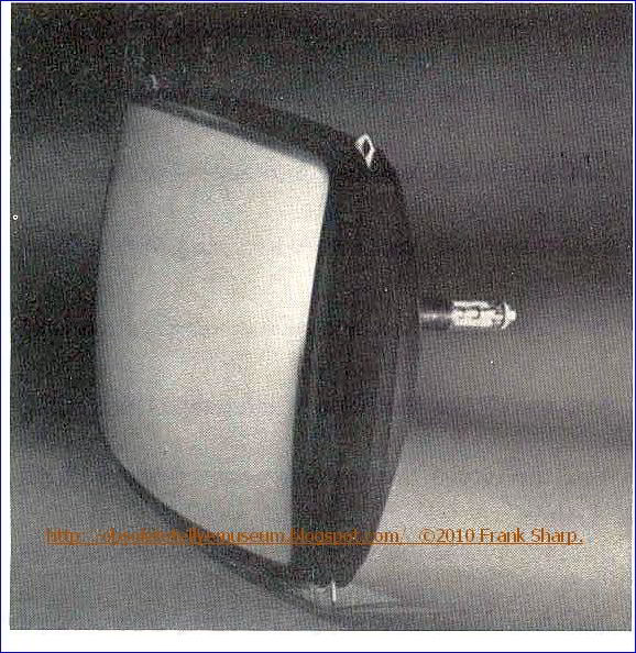 These requirements can be comparatively
easily satisfied in the case of the cathode-ray tube with a spherically
formed screen, whereas it is difficult to satisfy the requirements in
the case of a narrow-necked, wide-angle deflection cathode-ray tube. The wide angle deflection cathode-ray tube is advantageous in practical
use because the distance between the electron guns and the screen is
small and the screen is almost flat with a curvature approximate to that
of a flat surface; however, it is necessary to control the electron
beams so that the electron beams may be emitted exactly onto the 3-color
phosphor dots on the screen because the incident angle and distance of
the electron beams which reach the phosphor dots on the screen have the
values proper to respective phospher dots.
These requirements can be comparatively
easily satisfied in the case of the cathode-ray tube with a spherically
formed screen, whereas it is difficult to satisfy the requirements in
the case of a narrow-necked, wide-angle deflection cathode-ray tube. The wide angle deflection cathode-ray tube is advantageous in practical
use because the distance between the electron guns and the screen is
small and the screen is almost flat with a curvature approximate to that
of a flat surface; however, it is necessary to control the electron
beams so that the electron beams may be emitted exactly onto the 3-color
phosphor dots on the screen because the incident angle and distance of
the electron beams which reach the phosphor dots on the screen have the
values proper to respective phospher dots.  (1885-1940) in Dresden. Following the destruction of the plant during the bombing raids in 1945, Martin Mende (the founder's son) created a new company in Bremen in 1947, in a former Focke-Wulf plant, under the name North German Mende Broadcast GmbH.
The name was subsequently changed to Nordmende: subsequently the
company became one of the prominent German manufacturers of radios,
televisions, tape recorders and record players in the 1950s and 1960s.
(1885-1940) in Dresden. Following the destruction of the plant during the bombing raids in 1945, Martin Mende (the founder's son) created a new company in Bremen in 1947, in a former Focke-Wulf plant, under the name North German Mende Broadcast GmbH.
The name was subsequently changed to Nordmende: subsequently the
company became one of the prominent German manufacturers of radios,
televisions, tape recorders and record players in the 1950s and 1960s.
 Nordmende
was well known for its televisions throughout Ireland during the
1970s and 1980s, the company bought the rights to the name and
launched a range of white goods including fridges, freezers, washing machines, and dishwashers, alongside a revamped range of flat-screen TVs and stereos.
Nordmende
was well known for its televisions throughout Ireland during the
1970s and 1980s, the company bought the rights to the name and
launched a range of white goods including fridges, freezers, washing machines, and dishwashers, alongside a revamped range of flat-screen TVs and stereos.


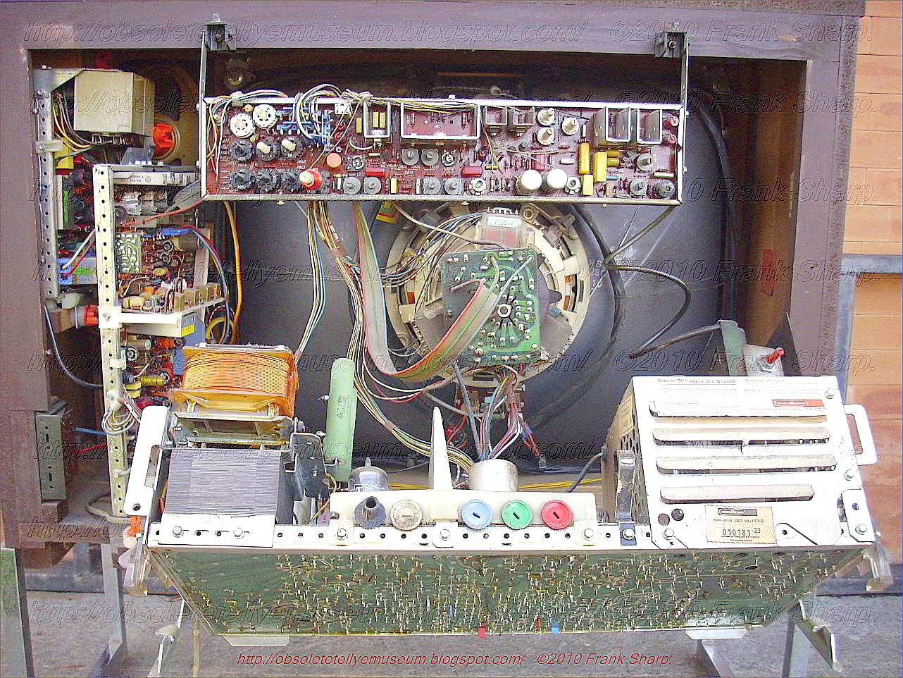


