Richtige Fernseher haben Röhren!

Richtige Fernseher haben Röhren!

In Brief: On this site you will find pictures and information about some of the electronic, electrical and electrotechnical Obsolete technology relics that the Frank Sharp Private museum has accumulated over the years .
Premise: There are lots of vintage electrical and electronic items that have not survived well or even completely disappeared and forgotten.

Or are not being collected nowadays in proportion to their significance or prevalence in their heyday, this is bad and the main part of the death land. The heavy, ugly sarcophagus; models with few endearing qualities, devices that have some over-riding disadvantage to ownership such as heavy weight,toxicity or inflated value when dismantled, tend to be under-represented by all but the most comprehensive collections and museums. They get relegated to the bottom of the wants list, derided as 'more trouble than they are worth', or just forgotten entirely. As a result, I started to notice gaps in the current representation of the history of electronic and electrical technology to the interested member of the public.

Following this idea around a bit, convinced me that a collection of the peculiar alone could not hope to survive on its own merits, but a museum that gave equal display space to the popular and the unpopular, would bring things to the attention of the average person that he has previously passed by or been shielded from. It's a matter of culture. From this, the Obsolete Technology Tellye Web Museum concept developed and all my other things too. It's an open platform for all electrical Electronic TV technology to have its few, but NOT last, moments of fame in a working, hand-on environment. We'll never own Colossus or Faraday's first transformer, but I can show things that you can't see at the Science Museum, and let you play with things that the Smithsonian can't allow people to touch, because my remit is different.

There was a society once that was the polar opposite of our disposable, junk society. A whole nation was built on the idea of placing quality before quantity in all things. The goal was not “more and newer,” but “better and higher" .This attitude was reflected not only in the manufacturing of material goods, but also in the realms of art and architecture, as well as in the social fabric of everyday life. The goal was for each new cohort of children to stand on a higher level than the preceding cohort: they were to be healthier, stronger, more intelligent, and more vibrant in every way.

The society that prioritized human, social and material quality is a Winner. Truly, it is the high point of all Western civilization. Consequently, its defeat meant the defeat of civilization itself.

Today, the West is headed for the abyss. For the ultimate fate of our disposable society is for that society itself to be disposed of. And this will happen sooner, rather than later.

OLD, but ORIGINAL, Well made, Funny, Not remotely controlled............. and not Made in CHINA.

How to use the site:
- If you landed here via any Search Engine, you will get what you searched for and you can search more using the search this blog feature provided by Google. You can visit more posts scrolling the left blog archive of all posts of the month/year,
or you can click on the main photo-page to start from the main page. Doing so it starts from the most recent post to the older post simple clicking on the Older Post button on the bottom of each page after reading , post after post.

You can even visit all posts, time to time, when reaching the bottom end of each page and click on the Older Post button.

- If you arrived here at the main page via bookmark you can visit all the site scrolling the left blog archive of all posts of the month/year pointing were you want , or more simple You can even visit all blog posts, from newer to older, clicking at the end of each bottom page on the Older Post button.
So you can see all the blog/site content surfing all pages in it.

- The search this blog feature provided by Google is a real search engine. If you're pointing particular things it will search IT for you; or you can place a brand name in the search query at your choice and visit all results page by page. It's useful since the content of the site is very large.

Note that if you don't find what you searched for, try it after a period of time; the site is a never ending job !

Every CRT Television saved let revive knowledge, thoughts, moments of the past life which will never return again.........

Many contemporary "televisions" (more correctly named as displays) would not have this level of staying power, many would ware out or require major services within just five years or less and of course, there is that perennial bug bear of planned obsolescence where components are deliberately designed to fail and, or manufactured with limited edition specificities..... and without considering........picture......sound........quality........
..............The bitterness of poor quality is remembered long after the sweetness of todays funny gadgets low price has faded from memory........ . . . . . .....
Don't forget the past, the end of the world is upon us! Pretty soon it will all turn to dust!

Have big FUN ! !
-----------------------
©2010, 2011, 2012, 2013, 2014 Frank Sharp - You do not have permission to copy photos and words from this blog, and any content may be never used it for auctions or commercial purposes, however feel free to post anything you see here with a courtesy link back, btw a link to the original post here , is mandatory.
All sets and apparates appearing here are property of Engineer Frank Sharp. NOTHING HERE IS FOR SALE !
All posts are presented here for informative, historical and educative purposes as applicable within Fair Use.


Wednesday, May 31, 2023

NORDMENDE SPECTRA 5177 YEAR 1984


The NORDMENDE SPECTRA 5177 is a 27  (67cm) inches color Stereo and BI-Sonic television with 39 programs and 99 channels PLL Synthesizer tuning CC4 Computer control 4..
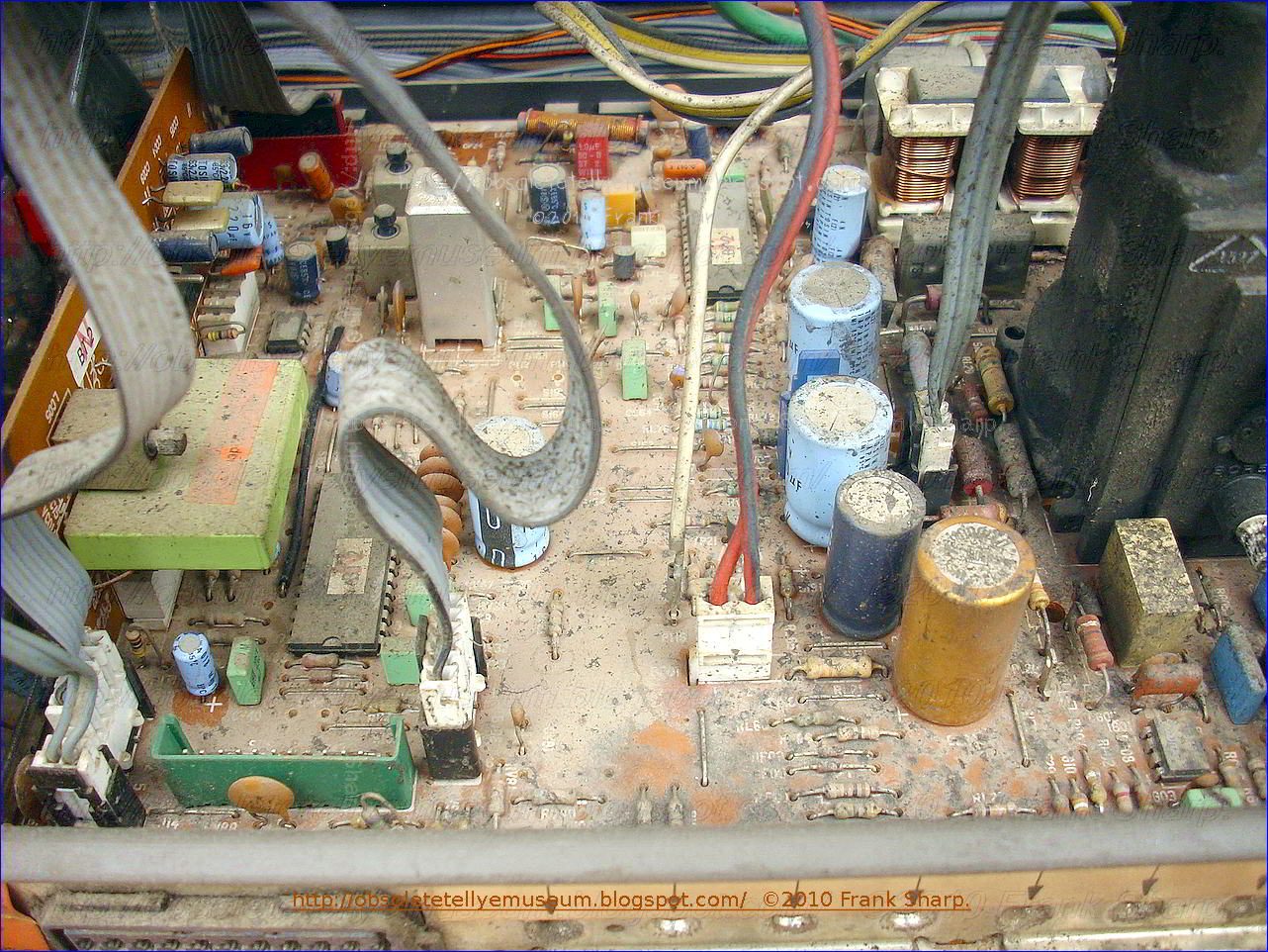
  • The set   introduces the new chassis Nordmende F11B but made by THOMSON as Chassis ICC3000. The set is indeed made entirely by THOMSON in Germany, as NORDMENDE was aquired by the French firm before. The THOMSON  Chassis ICC3000 was also shared in SABA TV, HITACHI (Some Models), TELEFUNKEN (Some Models) sets and  B&O TV sets.
  • Right side a red led  display shows programs and channels numbers with the "Pr x " and after the "Ch xx" for 2 seconds after, this during use of the set and a remote which controls the set. Such kind of displaying was also featured in future sets with other equipment chassis's.
  • Also a stereo headphone jack of a din type is present.
  • SCART connector  Is also present backside and first time it will feature all sets fabricated by the THOMSON firm from then to future.
The set introduces:New features of the chassis F 11 B: (THOMSON ICC3000)  respectfully to 1983 F11 (THOMSON ICC3)
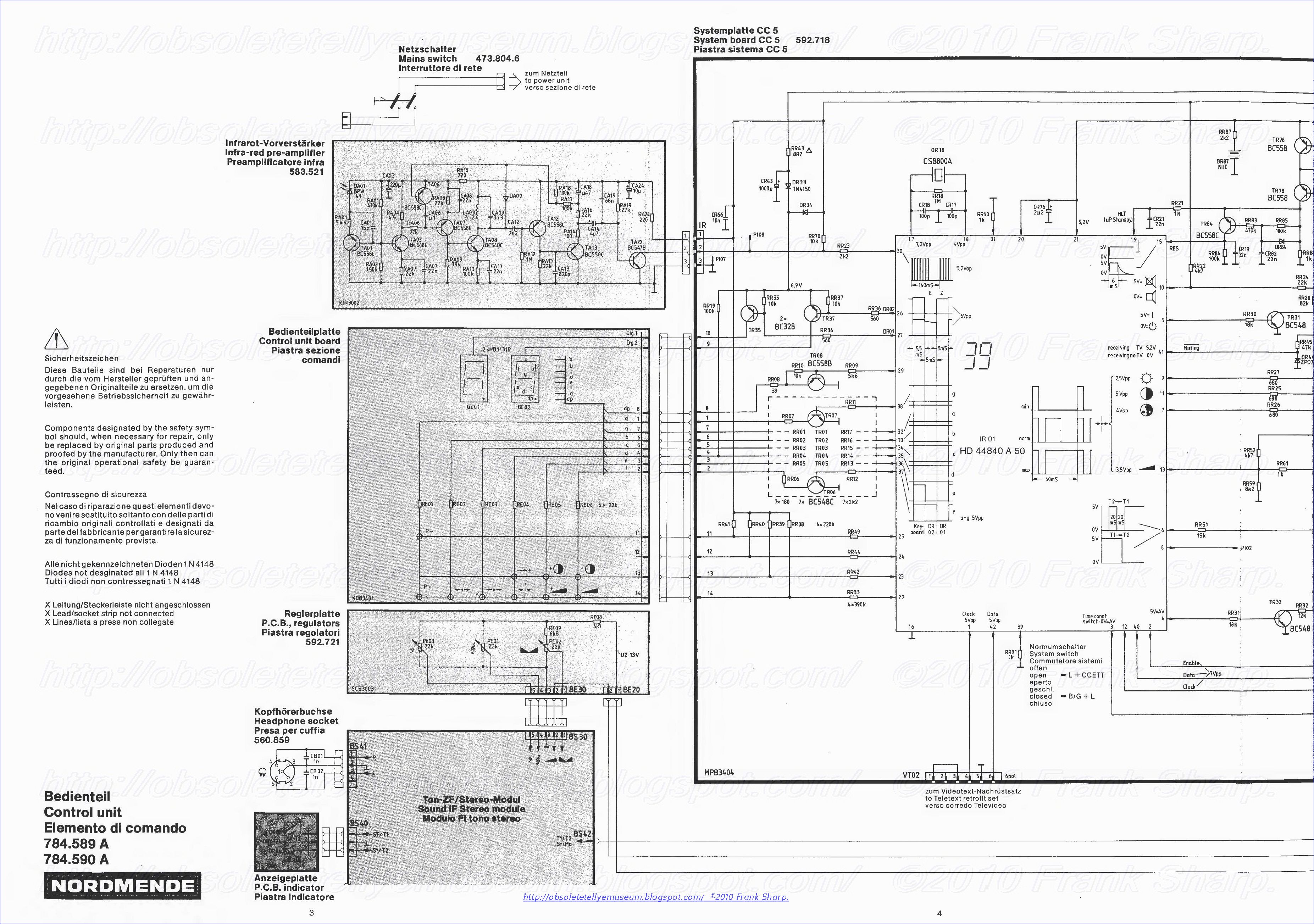
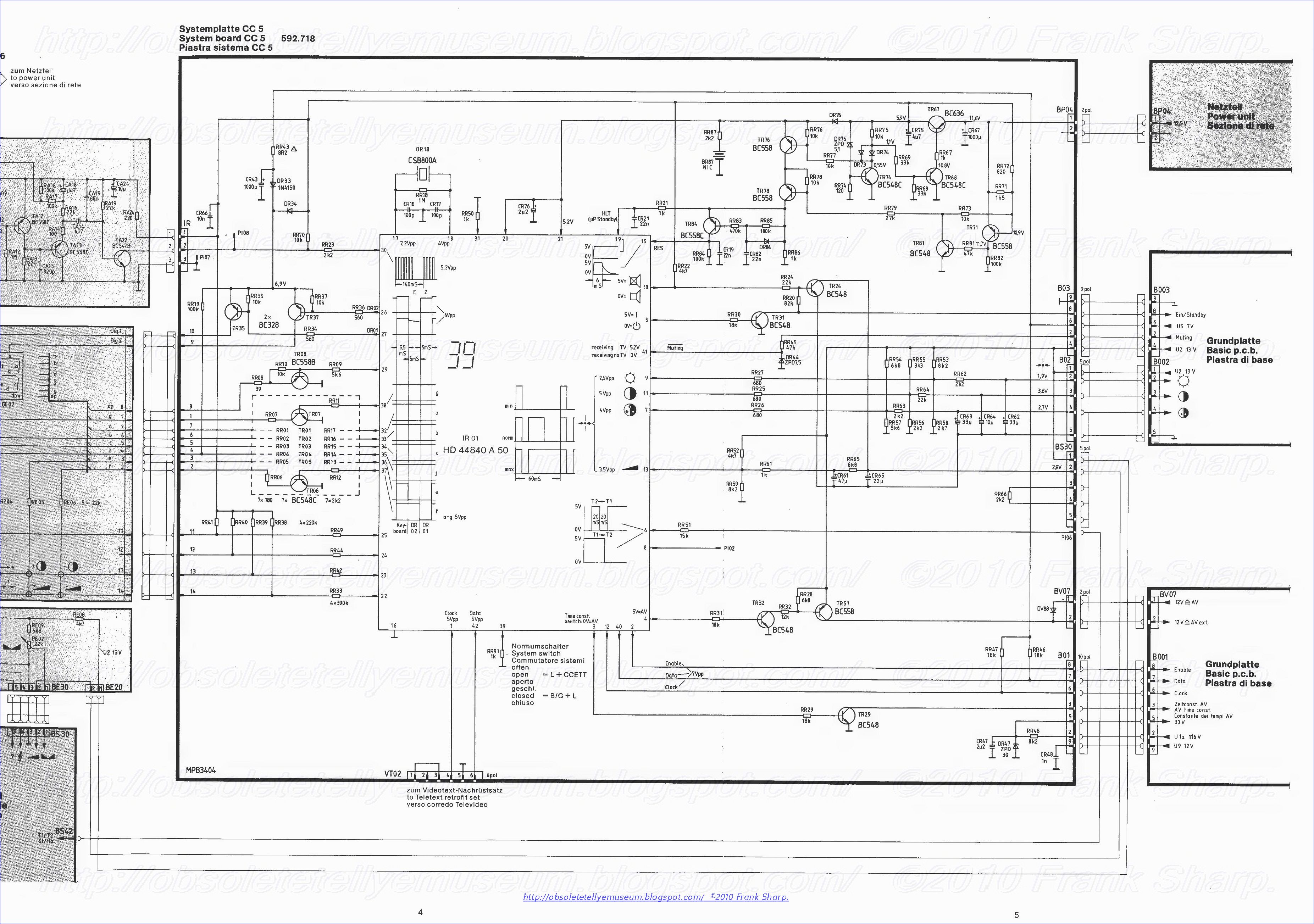
  • Integration  in the new IC TEA 2026:The vertical and horizontal frequencies are derived from a 500 kHz crystal oscillator and divider. Adjustment of the vertical and horizontal frequency is not required. vertical generator up to the control function of the vertical output thyristor, including automatic switching of the 50/60 Hz / horizontal generator up to the control of the horizontal output stage / switch mode power supply up to the control of the step-up transistor, including ‘soft- start’ and protection circuit
  • Stereo Sound and Bi Language sound channnel .
  • Switched-mode frame-scan control circuit for vertical deflection as featured earlier in F11 (1983) /Switched mode vertical deflection systems derive power from horizontal deflection energy, by storing a portion of a horizontal trace or retrace energy each horizontal deflection cycle. The energy is supplied to a vertical deflection winding in order to provide the desired vertical deflection current in the deflection winding. The amount of horizontal rate energy stored each horizontal interval is closely controlled in order to provide the correct amount of vertical deflection current. 
  •  First introduction of a a single case enclosing a device comprises inside a tuner, an intermediate frequency amplifier connected to the tuner, a demodulator connected to the intermediate frequency amplifier and sound IF, and a phase locked loop provision connected to the tuner.
  •  High integration chassis featuring all functions of the receiver.
  •  Additionally an optional teletext feature.
    A SCART Connector (which stands for Syndicat des Constructeurs d'Appareils Radiorécepteurs et Téléviseurs) is a standard for connecting audio-visual equipment together. The official standard for SCART is CENELEC document number EN 50049-1. SCART is also known as Péritel (especially in France) and Euroconnector but the name SCART will be used exclusively herein. The standard defines a 21-pin connector (herein after a SCART connector) for carrying analog television signals. Various pieces of equipment may be connected by cables having a plug fitting the SCART connectors. Television apparatuses commonly include one or more SCART connectors.
    Although a SCART connector is bidirectional, the present invention is concerned with the use of a SCART connector as an input connector for receiving signals into a television apparatus. A SCART connector can receive input television signals either in an RGB format in which the red, green and blue signals are received on Pins 15, 11 and 7, respectively, or alternatively in an S-Video format in which the luminance (Y) and chroma (C) signals are received on Pins 20 and 15. As a result of the common usage of Pin 15 in accordance with the SCART standard, a SCART connector cannot receive input television signals in an RGB format and in an S-Video format at the same time.
    Consequently many commercially available television apparatuses include a separate SCART connectors each dedicated to receive input television signals in one of an RGB format and an S-Video format. This limits the functionality of the SCART connectors. In practical terms, the number of SCART connectors which can be provided on a television apparatus is limited by cost and space considerations. However, different users wish the input a wide range of different combinations of formats of television signals, depending on the equipment they personally own and use. However, the provision of SCART connectors dedicated to input television signals in one of an RGB format and an S-Video format limits the overall connectivity of the television apparatus. Furthermore, for many users the different RGB format and S-Video format are confusing. Some users may not understand or may mistake the format of a television signal being supplied on a given cable from a given piece of equipment. This can result in the supply of input television signals of an inappropriate format for the SCART connector concerned.
    This kind of connector is todays obsoleted !


    PLL SYNTHESIZED TUNING System Concepts:

    INTRODUCTION Digital tuning systems are fast replacing the conventional mechanical systems in AM FM and television receivers The desirability of the digital approach is mainly due to the following features * Precise tuning of station frequencies
    * Exact digital frequency display
    * Keyboard entry of desired frequency
    * Virtually unlimited station memory
    * Up down scanning through the band
    * Station ‘‘search’’ (stop on next active station)
    * Power on to the last station
    * Easy option for time-of-day clock In addition
    " recent "developments in large scale integrated circuit technology and new varactor diodes for the AM band have made the cost-benefit picture for digital tuning very attractive System partitioning is extremely important in optimizing this cost-benefit picture as will be discussed.

    SYSTEM DESCRIPTION
    A simplified block diagram of a typical digitally tuned receiver is shown in Figure 1 Notice this receiver could be one for AM FM marine radio or television it makes no difference The frequency synthesizer block generates the local oscillator frequency for the receiver just as a conventional mechanical tuner would However the phase-locked-loop (PLL) acts as an integral frequency multiplier of an accurate crystal controlled reference frequency while the mechanical type provides a continuously variable frequency output with no reference Some method of controlling the value of the multiplier for channel tuning must be provided The other RF IF and audio video circuitry will be the same as in the mechanical tuning method There are many different ways to partition the frequency synthesizer system to perform the digital tuning function................


    The tuning is for this capable of 99 channels PLL synthesized tuner .
 
  The chassis used in this series was only produced for  a year or little more.
 For last time a Big powerful Supply transformer is used.
 An isolating power supply for electrical equipment comprises a transformer having an input for a mains alternating current (AC) power supply, a rectifier by which the output of the transformer can be rectified, and a primary energy storage device for electrically smoothing the output of the rectifier....A video apparatus, such as a television receiver or a computer monitor, may incorporate user accessible terminals or jacks to facilitate input or output of video or audio signals. These user accessible terminals or jacks must be electrically isolated from the AC line supply in order to protect the user from shock hazard. Electrical isolation may be provided by isolation transformers like the case here shown.
  • (To see the Internal Chassis Just click on Older Post Button on bottom page, that's simple !)


    NORDMENDE HISTORY

      Nordmende was a manufacturer of entertainment electronics based in Bremen, Germany.
    The original company, Radio H. Mende & Co, was founded in 1923 by Otto Hermann Mende (1885-1940) in Dresden. Following the destruction of the plant during the bombing raids in 1945, Martin Mende (the founder's son) created a new company in Bremen in 1947, in a former Focke-Wulf plant, under the name North German Mende Broadcast GmbH. The name was subsequently changed to Nordmende: subsequently the company became one of the prominent German manufacturers of radios, televisions, tape recorders and record players in the 1950s and 1960s.

    In the 1970s, Nordmende televisions were renowned for their innovative chassis, and for the rigorous testing and quality control of their finished products. Both created high costs, however, which soon proved a competitive disadvantage when the price of colour televisions began to plunge.
    In 1969, Mende's sons took over the company, and in 1977 a majority shareholding was sold to the French Thomson Brandt company and the chassis remains the original NordMende until CHASSIS F9. The following year, the family sold their remaining shares to Thomson. In the 1980s, the factories in Bremen were closed, Nordmende becoming purely a Thomson trademark (Starting from chassis F10 F11 they're all THOMSON).


    In the 1990s, the name Nordmende was used with decreasing frequency, and it eventually disappeared in favour of the Thomson name. In 2005 Videocon Group acquired all cathode ray tube activities from Thomson. This led to the creation of VDC Technologies, which manufactures TV sets using the Nordmende brand under licence from Thomson.
    The Nordmende brand name was relaunched in Ireland in September 2008 by the KAL Group. Although Nordmende was well known for its televisions throughout Ireland during the 1970s and 1980s, the company bought the rights to the name and launched a range of white goods including fridges, freezers, washing machines, and dishwashers, alongside a revamped range of flat-screen TVs and stereos.


    https://2.bp.blogspot.com/-02bRHy79G6E/UJv6EY6BbQI/AAAAAAAAM-s/9bOe6_W9778/s1600/NORDMENDE-L2UT-AD1.jpg
    The pre-war history can be found under Mende. After the total loss in Dresden, Martin Mende (Dec. 30, 1898-1982) founds Norddeutsche Mende-Rundfunk GmbH in Bremen-Hemelingen on August 26, 1947, with the assistance of Hermann Weber.

    • The first housings are supplied by a carpenter in Achim in exchange for five housings to make one radio set. The former Mende designer, Obering. Heer is again responsible for the equipment.
    • From July 27, 1948, the new company, first 18 and soon 60 people, supplies the new radio production on the basis of currency reform, loans and subcontracts.
    • The regime in East Germany does not allow the name Mende, so Martin Mende continues his pre-war success with graphic designs in connection with "Nord".
    • The hangars of the former Focke-Wulf AG near Seebaldsbrück station serve as workshops. In 1950, the company employs 700 people, in 1959 already 3500 and at its zenith 6300.
    • In 1950, the company starts with VHF, in 1953 with television and in 1954 with measuring and testing equipment. Towards the end of the 1950s, the company is called Norddeutsche Mende Rundfunk KG .

    Having not previously been involved with magnetic sound equipment, Nordmende launches the first German home tape recorder with three motors in 1958. However, other companies such as AEG/Telefunken and Grundig clearly dominate this sector. From Nordmende, only one or two devices (none in 1960) appear in the catalogs. But the company is successful with another new entry:


    In 1958, Nordmende introduces its first travel set, "Mambo" - but not "the first German, mass-produced and fully transistorized portable set," according to one source. After that, Nordmende becomes particularly strong in Germany in the travel set sector, although they did not build tube suitcases. After all, the 8 semiconductors used in "Mambo" then cost DM 98.70 at retail, while for the four D-tubes of the 90 series - even at the catalog price - about DM 35 would have to be spent. Price of the whole unit: DM 189.- plus two flat batteries of 4.5 V.

    Until 1969, there are about 92 models of portable radios (suitcase radios or "hand held radios"). For example, in the 1961/62 catalog, there are 11 table radios and radio furniture as well as 8 models of travel radios. 17 different television models, on the other hand, show where success was to be found in those days.

    According to ], Nordmende was even technically ahead for a short time with the so-called "Tippomatik operation". See also Philips etc.

    Also concert cabinets seem to be a mainstay for Nordmende in the late 50s to early 60s. The company repeatedly uses the same names like "Cabinet", "Caruso", "Casino", "Cosima" as well as "Arabella" and "Isobella" with changing additional numbers or the addition "Stereo", e.g. in 1959 and 1960/61.

    • In March 1967, the plant started production of color TV sets. For the company's anniversary, a series of sets called 'Golden 20' is published. In 1969, the Mende sons Karl and Hermann take over the management.
    • In 1977, increased competition leads to the sale of a majority stake to the French group Thomson-Brandt; the Mende family then withdraws completely from the company. Martin Mende dies in 1982.
    • In 1977, shares in the company were sold to the French Thomson-Brandt Group. A year later, the family also sold its remaining share in Thomson-Brandt.
    The Bremen-based company always consisted of two companies. Production was handled by Norddeutsche Mende Rundfunk KG; sales and advertising were handled by Nordmende Vertriebs GmbH & Co. oHG.


    • During Thomson's control, the production company changed its name several times: Norddeutsche AG für Unterhaltungselektronik & Co. oHG (NAGFU), later Deutsche AG für Unterhaltungselektronik & Co. oHG (DAGFU). DAGFU became the holding company for the German Thomson companies.
    • Production was transferred to Deutsche Elektronik-Werke GmbH (DEWEK), which was formed from Süddeutsche Elektronikwerke GmbH (SEWEK), the former SABA production company. In the late 1980s, DEWEK was merged with Norddeutsche Elektronikwerke GmbH (NEWEK), the Telefunken production company, to form Elektronik-Werke Deutschland GmbH (EWD). EWD later operated under the name Thomson Television Germany GmbH (TTG).
    • The sales company (oHG) was dissolved in the mid-1980s. Distribution in Germany was continued by Nordmende Vertriebs GmbH, which changed its name to Nordmende GmbH. Nordmende GmbH was merged with Telefunken Fernseh und Rundfunk GmbH with plants in Hanover and Celle, SABA GmbH, TTG and other companies in the mid-1990s to form Thomson Multimedia Sales GmbH.


    The other company involved in Nordmende Vertriebs GmbH & Co. oHG, Nordmende Verkaufs GmbH, changed its name to Nordmende International GmbH and, under the umbrella of European Consumer Electronics GmbH (ECE), held the trademark rights to Nordmende for the export business, while the export business itself was handled by ECE. Nordmende International GmbH was sold to Thomson Consumer Electronics S.A. in Paris in the mid-1990s, changed its name to Thomson Consumer Electronics GmbH and acquired a share in DAGFU, as a result of which DAGFU changed its name to Thomson Consumer Electronics GmbH & Co. oHG.


    Thomson's acquisition of Telefunken Fernseh und Rundfunk GmbH in Hanover in 1983 meant that all German Thomson production facilities now continued to operate under the name Elektronik Werke Deutschland (EWD).

    While at the Villingen-Schwenningen site of SABA (SEWEK), Thomson's complete television set development and chassis production (printed circuit boards) were combined and television production was discontinued, the Bremen plant advanced to become the headquarters of color television set assembly for Thomson's German and European subsidiary brands. Only Telefunken was still allowed to build its own sets with its own chassis at the Celle plant (closed in 1997) because of its strong position in the German market.

    Originally, Thomson had planned to close the Bremen site and abandon it completely. However, the company had not counted on the resistance of the employees and the support of the Bremen Senate and the great media response. Since Thomson already had a reputation in Germany as a "job killer" and did not want to put itself in a bad light again, the company backed down. Instead, production in Villingen-Schwenningen was closed and relocated to Bremen.

    Then, in the mid-1980s, the Bremen Thomson plant was also on the verge of going out of business. In 1987, the managing directors took over the company in a management buy-out. With the social plan funds from Thomson, an investment from the state-owned Hanseatische Industrie-Beteiligungen GmbH (HIBEG) and loans from leading Bremen banks, the television set and plastic parts production was continued with a greatly reduced workforce under the name Europart (the planned name was initially Eurotec).
    End of production

    At the end of the 1980s, after Thomson had stopped purchasing plastic parts from Europart for its television set production, which had been relocated in the meantime, the company plunged into a crisis from which it never recovered. The company's own developments were unable to establish themselves on the market in parallel with supplier production, so that despite rescue attempts by the Bremen Senate and a plant occupation lasting several weeks, the company went into insolvency because the banks had cancelled their credit lines.

    Nordmende brand under Thomson

    Immediately after acquiring the company, Thomson separated production and sales into two companies. While production was controlled directly from the headquarters in Paris, sales initially remained independent. The production of audio equipment was discontinued in Germany and relocated to France. After the closure of several factories in the Bremen area, the television production in Bremen and the Kit Center in Bremerhaven remained. At the Kit Center, kits were assembled for countries that required a domestic production content (local content).

    The main markets for Nordmende were Germany and Italy. Qualified specialist retailers were used as the sales channel in Germany and general importers for the export markets. After the export activities of the group brands Nordmende, Telefunken and SABA were combined under the umbrella of ECE GmbH in Hanover in 1987, domestic sales continued to operate independently from Bremen for several years.

    In the early 1990s, Thomson was forced to reorganize its domestic sales operations as a result of the cut-throat competition from low-cost large-scale sales organizations. The distribution of the Nordmende, Telefunken and SABA brands was centralized in Hanover. Brand families were established: SABA and Brandt (France) as price-oriented brands for the large-scale distribution forms, Telefunken as a quality brand for the retail trade, and Nordmende and Thomson (France) as design-oriented brands for the upper price segment.

    When the Thomson Group became involved in Germany, it avoided using the Thomson name for a long time, which was also expressed in company names such as SEWEK, EWD or DAGFU. In the 1990s, a change occurred. Various companies were rebranded with the Thomson name. As a final consequence, the Nordmende brand was also taken off the market and replaced by Thomson, which led to an even faster decline in Germany.
    Nordmende today

    Since the end of 2007, the Nordmende brand name has again appeared sporadically in connection with LCD televisions. The Indian consumer electronics group Videocon took over a television tube factory in Anagni, Italy, from the French Thomson Group, acquiring the trademark rights of the formerly traditional German brand Nordmende. The Phillar Group has been using the Nordmende name since 2008.

    In Italy in particular, design-oriented flat-screen televisions are sold under the Nordmende brand. Since 2014, the Nordmende brand name has also been used in connection with electronic hearing aid-like devices.

    In April 2017, TechniSat acquired the license to use the Nordmende brand for Germany, Austria, Switzerland as well as Poland from the brand owner Technicolor S.A.. The first Nordmende devices from the TV sets and DAB+ digital radios segments were presented at IFA 2017.


    NORDMENDE HISTORY IN GERMAN:

    Die Vorkriegsgeschichte findet sich unter Mende. Nach dem Totalverlust in Dresden gründet Martin Mende (30.12.1898-1982) unter Mitwirkung von Hermann Weber am 26. August 1947  in Bremen-Hemelingen die Norddeutsche Mende-Rundfunk GmbH.

    Die ersten Gehäuse liefert ein Tischler in Achim gegen Kompensation von fünf Gehäusen zu einem Rundfunkgerät. Der frühere Mende-Konstrukteur, Obering. Heer zeichnet wieder für die Geräte verantwortlich .

    Ab 27. Juli 1948 liefert die neue, zuerst 18 und bald 60 Personen umfassende Firma auf Grund von Währungsreform, Krediten und Zulieferverträgen die neue Radioproduktion.

    Das Regime in Ostdeutschland lässt den Namen Mende nicht zu, so dass Martin Mende mit grafischen Konstruktionen im Zusammenhang mit «Nord» an seinen Vorkriegserfolg anschliesst.

    Die Hallen der ehemaligen Focke-Wulf AG beim Bahnhof Seebaldsbrück dienen als Werkstätten. 1950 beschäftigt das Unternehmen 700, 1959 schon 3500 und im Zenit 6300 Personen.

    1950 beginnt die Firma mit UKW-, 1953 mit Fernseh- und 1954 mit Mess- und Prüfgeräten. Gegen Ende der 50er Jahre heisst die Firma Norddeutsche Mende Rundfunk KG .

    Nachdem sich Nordmende bislang nicht mit Magnettongeräten befasst hat, bringt das Werk 1958 das erste deutsche Heim-Tonbandgerät mit drei Motoren auf den Markt. Allerdings dominieren auf diesem Sektor eindeutig andere Firmen wie AEG/Telefunken und Grundig. Von Nordmende kommen jeweils nur ein bis zwei Geräte (1960 keines) in die Kataloge. Dafür hat die Firma Erfolg mit einem anderen Neueinstieg:


    1958 stellt Nordmende mit «Mambo» ihr erstes Reisegerät vor - aber nicht «das erste deutsche, serienmässig hergestellte und volltransistorisierte Koffergerät», wie man aus einer Quelle nachlesen kann. Danach wird Nordmende in Deutschland auf dem Sektor Reisegeräte besonders stark, obwohl sie keine Röhren-Koffer baute. Immerhin kosten die in «Mambo» verwendeten 8 Halbleiter dann im Einzelhandel DM 98.70, während für die vier D-Röhren der 90er-Serie - auch zum Katalogpreis - etwa DM 35.- auszugeben wären. Preis des ganzen Gerätes: DM 189.- plus zwei Flachbatterien von 4,5 V.

    Bis 1969 gibt es ca. 92 Modelle der tragbaren Radios (Koffer- bzw. «Handradios», d.h. «Hand held radios»). Beispielsweise finden sich im Katalog 1961/62  je 11 Tischradios und Radiomöbel sowie 8 Modelle von Reiseradios. 17 verschiedene Fernsehmodelle zeigen dagegen, wo in jener Zeit der Erfolg zu holen war.

    Gemäss ] liegt Nordmende während kurzer Zeit mit der sogenannten «Tippomatik-Bedienung» sogar technisch vorne. Siehe auch Philips etc.

    Auch Konzertschränke scheinen Ende der 50er bis Anfang 60er Jahre eine tragende Säule für Nordmende zu sein. Dabei verwendet die Firma immer wieder gleiche Namen wie «Cabinet», «Caruso», «Casino», «Cosima» sowie «Arabella» und «Isobella» mit wechselnden Zusatz-Nummern oder den Zusatz «Stereo», z.B. in den Jahren 1959 und 1960/61.

    Im März 1967 nimmt das Werk die Produktion von Farbfernsehgeräten auf. Zum Firmenjubiläum erscheint eine Gerätereihe mit der Bezeichnung 'Goldene 20'. 1969 übernehmen die Mende-Söhne Karl und Hermann die Geschäftsführung.

    1977 führt der verschärfte Wettbewerb zum Verkauf der Mehrheit an den französischen Konzern Thomson-Brandt; die Familie Mende zieht sich anschliessend ganz aus dem Unternehmen zurück. Martin Mende stirbt 1982.

    1977 wurden Anteile des Unternehmens an den französischen Thomson-Brandt-Konzern verkauft. Ein Jahr später veräußerte die Familie auch ihren verbliebenen Anteil an Thomson-Brandt.
    Das Bremer Unternehmen bestand stets aus zwei Gesellschaften. Die Produktion erfolgte bei der Norddeutsche Mende Rundfunk KG; den Vertrieb und die Werbung übernahm die Nordmende Vertriebs GmbH & Co. oHG.


    Während der Beherrschung durch Thomson änderte die Produktionsgesellschaft mehrfach ihren Namen: Norddeutsche AG für Unterhaltungselektronik & Co. oHG (NAGFU), später Deutsche AG für Unterhaltungselektronik & Co. oHG (DAGFU). Die DAGFU wurde zur Holding der deutschen Thomson-Gesellschaften.


    Die Produktion ging auf die Deutschen Elektronik-Werke GmbH (DEWEK) über, die aus der Süddeutschen Elektronikwerke GmbH (SEWEK), der ehemaligen SABA-Produktionsgesellschaft, entstanden ist. Ende der 1980er Jahre wurde die DEWEK mit der Norddeutschen Elektronikwerke GmbH (NEWEK), der Telefunken-Produktionsgesellschaft, zur Elektronik-Werke Deutschland GmbH (EWD) fusioniert. Die EWD firmierte später als Thomson Television Germany GmbH (TTG).


    Die Vertriebsgesellschaft (oHG) wurde Mitte der 1980er Jahre aufgelöst. Der Vertrieb in Deutschland wurde von der Nordmende Vertriebs GmbH fortgeführt, die sich in Nordmende GmbH umbenannte. Die Nordmende GmbH wurde Mitte der 1990er Jahre zusammen mit der Telefunken Fernseh und Rundfunk GmbH mit Werken in Hannover und Celle, der SABA GmbH, der TTG und anderen Gesellschaften zur Thomson Multimedia Sales GmbH verschmolzen.


    Die andere, an der Nordmende Vertriebs GmbH & Co. oHG beteiligte Gesellschaft, die Nordmende Verkaufs GmbH, firmierte in Nordmende International GmbH um und hielt unter dem Dach der European Consumer Electronics GmbH (ECE) die Markenrechte an Nordmende für das Export-Geschäft, während das Export-Geschäft an sich von der ECE wahrgenommen wurde. Die Nordmende International GmbH wurde Mitte der 1990er Jahre an die Thomson Consumer Electronics S.A. in Paris verkauft, firmierte in Thomson Consumer Electronics GmbH um und erwarb einen Anteil an der DAGFU, wodurch die DAGFU in Thomson Consumer Electronics GmbH & Co. oHG umfirmierte.


    Durch Thomsons Übernahme der Telefunken Fernseh und Rundfunk GmbH in Hannover im Jahr 1983 wurden nunmehr alle deutschen Thomson-Produktionsstätten unter dem Namen Elektronik Werke Deutschland (EWD) weitergeführt.

    Während am Standort Villingen-Schwenningen bei SABA (SEWEK) die komplette Fernsehgeräte-Entwicklung und Chassis-Produktion (Leiterplatten) von Thomson zusammengefasst und die Fernseher-Produktion aufgegeben wurde, avancierte das Bremer Werk zur Zentrale der Farbfernsehgerätemontage der deutschen und europäischen Thomson-Tochtermarken. Lediglich Telefunken durfte im Werk Celle (1997 geschlossen) wegen seiner starken Position am deutschen Markt noch eigene Geräte mit eigenem Chassis bauen.

    Ursprünglich hatte Thomson geplant, den Standort Bremen zu schließen und komplett aufzugeben. Der Konzern hatte jedoch nicht mit dem Widerstand der Beschäftigten und der Unterstützung durch den Bremer Senat und dem großen Medienecho gerechnet. Da Thomson in Deutschland bereits einen Ruf als „Jobkiller“ hatte und sich nicht erneut ins schlechte Licht rücken wollte, machte das Unternehmen einen Rückzieher. Stattdessen wurde die Produktion in Villingen-Schwenningen geschlossen und nach Bremen verlagert.

    Mitte der 1980er Jahre stand dann auch das Bremer Thomson-Werk vor dem Aus. 1987 übernahmen die Geschäftsführer im Zuge eines Management Buy Outs das Unternehmen. Mit den Sozialplan - Geldern von Thomson, einer Beteiligung der landeseigenen Hanseatischen Industrie-Beteiligungen GmbH (HIBEG) und Krediten führender Bremer Banken wurden die Fernsehgeräte- und Kunststoff teile produktion, mit einer stark reduzierten Belegschaft, unter dem Namen Europart (geplanter Name war zunächst Eurotec) fortgeführt.
    Ende der Produktion

    Nachdem Thomson Ende der 1980er Jahre seine Kunststoffteile für die inzwischen verlagerte Fernsehgeräte produktion nicht mehr von Europart bezog, stürzte das Unternehmen in eine Krise, von der es sich nicht mehr erholte. Eigene Entwicklungen konnten sich parallel zur Zulieferproduktion am Markt nicht etablieren, so dass das Unternehmen trotz der Rettungsversuche durch den Bremer Senat und einer mehrwöchigen Werksbesetzung in die Insolvenz ging, da die Banken ihre Kreditlinien gekündigt hatten.

    Marke Nordmende unter Thomson

    Unverzüglich nach Erwerb des Unternehmens trennte Thomson Produktion und Vertrieb in zwei Gesellschaften auf. Während die Produktion direkt von der Zentrale in Paris gesteuert wurde, blieb der Vertrieb zunächst eigenständig. Die Produktion von Audio-Geräten wurde in Deutschland eingestellt und nach Frankreich verlagert. Nach Schließung mehrerer Fabriken im Bremer Umland blieben die Fernsehproduktion in Bremen und das Kit Center in Bremerhaven übrig. Im Kit Center wurden Bausätze für Länder zusammengestellt, die einen inländischen Produktionsanteil (local content) forderten.

    Die Hauptmärkte für Nordmende waren Deutschland und Italien. Als Vertriebskanal in Deutschland wurde der qualifizierte Facheinzelhandel und für die Exportmärkte Generalimporteure genutzt. Nachdem die Exportaktivitäten der Konzernmarken Nordmende, Telefunken und SABA im Jahr 1987 unter dem Dach der ECE GmbH in Hannover zusammengefasst worden waren, agierte der Inlandsvertrieb noch einige Jahre eigenständig von Bremen aus.

    Durch den Verdrängungswettbewerb der preisgünstigen Großvertriebsformen sah sich Thomson Anfang der neunziger Jahre gezwungen, den Inlandsvertrieb neuzuordnen. Die Vertriebe der Marken Nordmende, Telefunken und SABA wurden in Hannover zentralisiert. Es wurden Markenfamilien gegründet: SABA und Brandt (Frankreich) als preisorientierte Marken für die Großvertriebsformen, Telefunken als Qualitätsmarke für den Einzelfachhandel sowie Nordmende und Thomson (Frankreich) als designorientierte Marken für das gehobene Preissegment.

    Als der Thomson-Konzern sich in Deutschland engagierte, wurde es lange Zeit vermieden, unter dem Namen Thomson aufzutreten, was sich auch in Gesellschaftsbezeichnungen wie SEWEK, EWD oder DAGFU ausdrückte. In den 1990er Jahren trat ein Wandel ein. Verschiedene Gesellschaften wurden mit dem Namensbestandteil Thomson umfirmiert. Als letzte Konsequenz wurde auch die Marke Nordmende vom Markt genommen und durch Thomson ersetzt, was zu einem noch schnelleren Niedergang in Deutschland führte.
    Nordmende heute

    Seit Ende 2007 taucht wieder vereinzelt der Markenname Nordmende in Zusammenhang mit LCD-Fernsehgeräten auf. Der indische Unterhaltungselektronik-Konzern Videocon hat von der französischen Thomson-Gruppe ein Fernsehröhrenwerk im italienischen Anagni übernommen und dabei die Markenrechte der ehemals deutschen Traditionsmarke Nordmende erworben. Seit 2008 verwendet die Phillar Group die Bezeichnung Nordmende.

    Besonders in Italien werden unter der Marke Nordmende gestaltungsorientierte Flachbild-Fernsehgeräte vertrieben. Seit 2014 wird der Markenname Nordmende auch im Zusammenhang mit elektronischen hörgeräteähnlichen Geräten verwendet.

    Im April 2017 erwarb TechniSat vom Markeninhaber Technicolor S.A. die Lizenz zur Nutzung der Marke Nordmende für Deutschland, Österreich, Schweiz sowie Polen. Zur IFA 2017 wurden die ersten Nordmende-Geräte aus den Segmenten TV-Geräte und DAB+-Digitalradios präsentiert.


    In 1879 Elihu Thomson and Edwin Houston formed the Thomson-Houston Electric Company in the United States.

    On April 15, 1892 Thomson-Houston and the Edison General Electric Company merged to form General Electric (GE). Also in 1892 the company formed a French subsidiary, Thomson Houston International.
    In 1893 Compagnie Française Thomson-Houston (CFTH) was set up as a partner to GE. It is from this company that the modern Thomson companies would evolve.
    In 1966 CFTH merged with Hotchkiss-Brandt to form Thomson-Houston-Hotchkiss-Brandt (soon renamed Thomson-Brandt). In 1968 the electronics business of Thomson-Brandt merged with Compagnie Générale de Télégraphie Sans Fil (CSF) to form Thomson-CSF. Thomson Brandt maintained a significant shareholding in this company (approximately 40%).
    In 1982 both Thomson-Brandt and Thomson-CSF were nationalized by François Mitterrand. Thomson-Brandt was renamed Thomson SA (Société Anonyme) and merged with Thomson-CSF.
    From 1983 to 1987 a major reorganisation of Thomson-CSF was undertaken, with divestitures to refocus the group on its core activities (electronics and defence). Thomson-CSF Téléphone and the medical division were sold to Alcatel and GE respectively. The semiconductor businesses of Thomson CSF was merged with Finmeccanica. Thomson acquired General Electric’s RCA and GE consumer electronics business in 1987.
    In 1988 Thomson Consumer Electronics was formed, renamed Thomson Multimedia in 1995. The French government split the consumer electronics and defence businesses prior to privatisation in 1999, those companies being Thomson Multimedia (today Technicolor SA) and Thomson-CSF (today Thales Group).


    Thomson-CSF was a major electronics and defence contractor. In December 2000 it was renamed Thales Group.


    ...........1996............there are no stranger foreigners than the first ones you come across, the French. This is borne out by the 1996 Thomson situation. Thomson, was a vast company by any reckoning, is a strange beast. It's state controlled, which means that the government owns most but not quite all of it. and consists of two distinct arms, the defence group Thomson-CFS which is quite profitable, and the consumer electronics group Thomson Multimedia which loses a packet. The government wanted  rid of it, but won't sell the bits separately. It doesn't want to be left with the problem of what to do with Thomson Multimedia. You might think that no one would be interested in helping the French government. But in fact there are two contenders to take over Thomson, the telecommunications and power group Alcatel Alsthom and the defence and media group Lagardere. They have been engaging in quite a battle over the ownership, and as we go to press the French government is due to decide whose bid to accept. Whoever wins will end up with the profitable defence company  and the problem of Thomson Multimedia (TMM).

    Lagardere has stated that it would sell TMM to Daewoo of Korea. Alcatel Alsthom has not been quite so specific, but has announced that it would take immediate action to reduce TMM's losses and seek an "Asian partner" that "specialises in consumer electronics". The partner would be expected to take over management of TMM, but Alcatel would like to remain a "minority partner" - it sees prospects in the move to digital TV technology that will occur during the next decade. All this gives one a strange feeling of déjà vu. At the time when Thomson took over Ferguson, in June 1987, it was noticed  that Thomson is "now on the government's privatisation list". It's taken almost a decade to happen.

     It's also said that "Thomson may be big, but has not been all that successful in the past in the consumer electronics field". Right on! What has happened to Ferguson in the UK illustrates the dismal Thomson effect. From being the local brand leader, with over ten per cent of the market, Ferguson has ended up being an also ran. It's only fair however to mention that Ferguson was making substantial losses when Thorn EMI was glad to get £90m for it from Thomson. Thomson has been able to survive in the consumer electronics field because it is part of a larger organisation, with those defence profits. It has nevertheless over the years attempted to play a a major role in the international consumer electronics field, keeping up with Philips and the Japanese corporations. From its French origins, it first expanded by picking up various German companies such as NordMende an SABA. It added Telefunken, a venerable name if ever there was one in this industry, in the early eighties, then took what was to be a big move into the UK market when it bought Ferguson. 

    It  used six brand names in Europe. The largest step however occurred when TMM became a major force in the North American market by taking over General Electric's consumer electronics interests. This also gave it the RCA operation. The idea behind all this seems to have been to achieve success simply by getting bigger. There was always government finance to back the policy, which in the event has not been a success. The TMM debacle is a sad one, since Thomson's research and engineering has had many successes.
     It has not stinted on R and D work, with laboratories in Los Angeles, Indianapolis, Strasbourg, Hanover, Villingen, Tokyo and Singapore. Much work has been done on HD -TV, digital signal processing and other developments that have kept it in the forefront of the technology. Now, it seems, TMM is likely to be swallowed up by one of the Oriental corporate giants. 
    If there are any lessons to be drawn, they would seem to be that expansion by itself is no guarantee of success, that to spread ones activities and their control across the globe makes management extremely difficult, and that costs are very hard to control in such a context. Alcatel Alsthom's plans to reduce TMM's losses bear this out. It would close down TMM's US factories, transferring production to the company's modern facilities in Mexico, where wages are much lower.

     It would rationalise the large collection of brands, possibly adopting RCA as the main one worldwide. And there is a suggestion that the company should be run from the USA, since this is its largest market. But all this would be just initial steps towards ceding majority control. Venerable brand names such as Telefunken, GE and RCA would pass to oriental ownership. This will happen whoever wins, Alcatel Alsthom or Lagardere, which would leave just Philips to carry on Europe's traditions in the consumer electronics field............. but we all know how it ended.................

    Thomson-CSF independence

    Following the privatisation of the Thomson Group Thomson-CSF explored the possibility of merging with Marconi Electronic Systems, however British Aerospace was successful in that aim, forming BAE Systems.
    In 2000 Thomson-CSF went through a series of transactions, including with Marconi plc. The major acquisition at this time was the £1.3 billion purchase of the British defence electronics firm, Racal. This made Thomson-CSF the second largest participant in the UK defence industry after BAE. Racal was renamed Thomson-CSF Racal plc.
    On December 6, 2000 the group was renamed Thales.

    ------------------------------------------------------------------------------------------------------------


    Further reading

  • Jean-Pierre, Thierry (16 October 2003). Taïwan Connection : Scandales et meurtres au cœur de la République [Taiwan Connection – Scandals and Murders at the Heart of the Republic] (in French). Robert Laffont. ISBN 978-2221100820.
  • L'entreprise partagée ? Une pratique différente des relations sociales : l'expérience Thomson-CSF, Robert Thomas (pseudonym for a team-work with Pierre Beretti and Jean-Pierre Thiollet), Paris, Maxima-Laurent du Mesnil Ed., 1999
Tote Marke NORDMENDE – Verblasster Stolz. Artikel im Manager-Magazin
«Annual Report 2010». STMicroelectronics. Consultado el 17 de noviembre de 2011.
Castelletto en ST


http://www.st.com/content/st_com/en/contact-us.html#EUROPE

«SGS-Thomson Microelectronics Becomes STMicroelectronics | EE Times». EETimes. Consultado el 6 de julio de 2017.

Peter Robin Morris (1990). A History of the World Semiconductor Industry. The Institution of Engineering and Technology. ISBN 9780863412271.

Okada, Yoshitaka (2006). Struggles for Survival. Institutional and Organizational Changes in Japan's High-Tech Industries. Springer. ISBN 9784431288749.

Franco Malerba (1985). The Semiconductor Business: The Economics of Rapid Growth and Decline (Economics of Technological Change). Madison, University of Wisconsin Press. ISBN 9780299104603.


 «China puts hopes in Loongson CPU». Linux.com | The source for Linux information (en inglés).


NORDMENDE SPECTRA 5177 CHASSIS F11B (THOMSON ICC3000) INTERNAL VIEW


NORDMENDE SPECTRA 5177  CHASSIS F11B (THOMSON ICC3000) 

The chassis is a monocarrier with all function exception for the frontend tuning controls.The metal box is containing the tuner VHF UHF unit plus the if stages and the PLL synthesizer section.
The power supply is derived from a mains transformer generating all supply.
Additional +B power supply is generated on the ICC3000 chassis board via SMPS power step-up type with line synchronized signals.

 Is the last chassis type  using a separation mains transformer in "BIG" Style.

 New features of the chassis F 11 B: (THOMSON ICC3000)  respectfully to F11 (THOMSON ICC3)


New developed iC TDA 4950 for the East/West correction.

Integration of the following stages in the new IC TEA 2026:
—  vertical generator up to the control function of the vertical output thyristor, including automatic switching of the 50/60 Hz standard frame frequency
—  horizontal generator up to the control of the horizontal output stage
—   switch mode power supply up to the control of the step-up transistor, including ‘soft- start’ and protection circuit
—  muting circuit
—  super-sandcastle-pulse generation
 
The vertical and horizontal frequencies are derived from a 500 kHz crystal oscillator and divider. Adjustment of the vertical and horizontal frequency is not required.


NORDMENDE SPECTRA 5177  CHASSIS F11B (THOMSON ICC3000)  Function description

1. Power Supply
1.1 Function principle
The power supply is also called ‘step-up’ circuit which raises the primary voltage U 8 (110 V) to 145 V and stabilises it. The switching transistor TP 01 is controlled by IL 01 (pin 7) to conduct during horizontal trace time. Due to the current which flows through LP 01, TP 01, RP 03 to ground, the coil LP 01 is charged with magnetic energy. A negative flyback pulse from the EHT transformer (pin 11) is fed via DP 44, DP 43 and RP 05 to the base of TP 01 and blocks the transistor instantly. The collapsing magnetic field within the coil LP 01 is causing an induction voltage, which is superimposed to the voltage U8(110 V) and charges CP 14 via DP 14. The additional components DP 10, RP 08, CP 23 prevent to high voltage peaks on DP 14, which is a slow acting type.


1.2 Start function
After switching on the mains switch the mains transformer UP 41 supplies the operating volt- age U8 110 V to the switch mode circuit and the start voltage 12,5 V. The voltage U 8 forms the preliminary operating voltage for the horizontal output stage as long as the switch mode power supply is not working and is fed over FP 02, LP 01,DP 14 and RP 14 to pin 8 of the EHT transformer. The driver transistor TL 01 is supplied with the start voltage (12,5 V) via the decoupling diode DP 13. As soon as a L-signal is supplied from the operating unit to the base of TP 21, the start voltage is fed to lL 01 via DP 21,DP 24, DPO3 and RP 27. The flyback transformer starts oscillating. The switching voltage of the three diodes mentioned determine the timing so, that at first the collector voltage is present on TL 01 and there- after the control signal. The horizontal output stage starts and the EHT- transformer generates the different operating voltages. The driver transistor TL 01 is now sup- plied with U 3 (21 V) via DP
23 and transistor TP 21 with voltage U 2a (13 V) via DP 15. Shortly after switch on and after the voltage on pin 8 of IC —IL 01 TEA 2026 has reached 6 V the vertical and the horizontal generator start to work. Because of the soft start circuit the switch mode power supply starts gradually to operate causing a transient current which is consequently very small and increases gradually to it's normal value.

1.3 Control function
A part of the operating voltage U 1 is reduced by a voltage divider RL 46, PP 01 and RL 47 and is fed to pin 9 of IL 01. This voltage is compared in- side the IC with a reference voltage of 1,26 V and controls thereafter the phase modulator, which in turn controls TP 01 slower or faster. If for _ instance the operating voltage U 1 is decreasing due to a high load or because of mains volt- age fluctuations, then the transistor TP 01 will be switched earlier. The loading coil LP 01 will thus be charged with higher energy and leads this energy after TP 01 is blocked via DP 14 to CP 14. Consequently U 1 rises again to it’s nominal value.

1.4 Protection circuit
If the reference voltage on pin 28 of IL 01 exceeds 1,26 V, then the vertical and horizontal deflection circuits as well as the switch mode power supply are cut off until the reference volt- age decreases again below 1,26 V and the switch mode power supply will be started again by the ‘soft-start’ system. If this cycled has repeated 3 times, then the set will be finally switched off: A new start is now only possible, if the operating voltage on pin 8 of IL 01 was previously on zero. In case U 1 increases too high, then also U 3 (21 V) will increase. The Zener  diode DF 25 will now conduct and raises the voltage via RF 30 on pin 28 of IL 01. The protection circuit will now go in action. In case of too much power consumption of the set the TP 01 will be overloaded. An increased voltage drop across RP 03 is then registered and is fed via RP 04 and RF 30  to control the protection circuit.

NORDMENDE SPECTRA 5177  CHASSIS F11B (THOMSON ICC3000) Switching regulator power supply device combined with the horizontal deflection circuit of a television receiver which it supplies

Step-up switching regulator power supply device comprising, connected between the poles of a rectifier circuit supplied by an isolating voltage step-down transformer and loaded by a first filter capacitor, and inductance and the collector-emitter path of a first switching transistor of NPN type, a first diode whose anode is connected to the junction of the inductance and to the collector of said transistor and whose cathode is connected to a second filter and storage capacitor supplying a voltage at its output which supplies a horizontal deflection circuit of a television receiver.
This horizontal deflection circuit which comprises in cascade a horizontal oscillator, a driver stage and an output stage, forms an integral part of the circuit controlling said first transistor and determines the repetition period of the switching, because it is started under an initial voltage slightly less than the unregulated input voltage of the device.
The switching transistor is being turned off in synchronism with the turning off of the trace switch transistor by using flyback pulses of negative polarity to bias the base thereof.

1. A power supply device with switching regulation and boosting of its DC output voltage, combined with a horizontal deflection circuit of a television receiver, supplied thereby and which comprises in cascade a horizontal oscillator, a driver stage and an output stage including a trace switch transistor and a line transformer, this device comprising an inductance and the collector-emitter path of a switching transistor connected in series between the poles of a DC input voltage source, a rectifying diode connected by its anode to the junction between the inductance and the collector of said switching transistor and by its cathode to one of the terminals of a filtering and storage capacitor whose other terminal is connected to the emitter of said transistor, so as to apply across its terminals an initial DC voltage slightly lower than said input voltage, when said switching transistor is turned off, and a regulated DC output voltage with a level higher than said input voltage, when said transistor is recurrently, alternately turned on and off, the level of said output voltage depending on the duty cycle of said switching transistor states, and a control circuit feeding the base of said switching transistor and including a regulator stage comparing an adjustable fraction of said output voltage to a fixed reference voltage and supplying a regulating current or voltage proportional to the difference between said compared voltages, a pulse-width modulator triggered by means of a recurrent signal and supplying a rectangular signal whose duty cycle varies as a function of said regulating current or voltage, another driver stage receiving the rectangular signal and controlling said switching transistor, the regulation and boosting of said output voltage being controlled by the initially independent starting up of the entire horizontal deflection circuit when supplied by said initial voltage from said power supply device as soon as a DC input voltage is applied thereto and which then delivers recurrent trigger pulses to said pulse-width modulator, one of the supply inputs of said other driver stage receiving directly a first voltage waveform whose positive alternations comprise constant-voltage plateau and whose negative alternations comprise negative-going horizontal flyback pulses provided by a first secondary winding of said line transformer, so as to control the turning off of said switching transistor substantially simultaneously with that of the trace switch transistor.

2. A power supply device as claimed in claim 1, wherein said other driver circuit comprises a third transistor whose emitter is connected to the base of said switching transistor and which is of the same type as the latter, whose collector is connected, through said supply input, to said first secondary winding of said line transformer to receive therefrom said first waveform and whose base is coupled to the output of said pulse-width modulator.

3. A power supply device as claimed in claim 2, wherein the collector of said third transistor is connected, through a resistor to the supply input and its emitter is connected, furthermore, to that of the switching transistor through another resistor so that the negative-going flyback pulses, applied to the collector of said third transistor, control the symmetric (reverse) saturation thereof so as to reversely bias the base-emitter junction of said switching transistor.

4. A power supply device as claimed in claim 2, wherein the collector of said third transistor is connected to said power supply input through a fourth diode conducting in the normal direction of its collector-emitter path, and wherein its emitter is further connected, on the one hand, through a resistor, to the emitter of the switching transistor and, on the other hand, through another resistor and a fifth diode conducting in the reverse direction to that of the base-emitter junction of the switching transistor, so as to transmit to the base thereof negative-going flyback pulses through a voltage divider formed by said two resistors in series.

5. A power supply device as claimed in claim 1, wherein said other driver circuit comprises a third transistor whose emitter is connected to the base of said switching transistor, whose collector is connected to that of this latter so as to form a so-called Darlington circuit and whose base coupled, moreover, to said pulse-width modulator is further connected, through a resistor and a diode in series, to said first secondary winding of said line transformer so as to control the simultaneous turn off of both transistors of said Darlington circuit by simultaneously reversely biasing their respective base-emitter junctions, connected in series, by means of negative-going flyback pulses.

6. A power supply device as claimed in any one of the preceding claims, wherein said pulse-width modulator, supplied at its input with a voltage waveform whose positive alternations comprise positive-going flyback pulses and whose negative alternations comprise constant negative-voltage plateaux, comprises a passive circuit which forms a simple integrator during positive alternations because one of its resistors is shunted by a diode and which is a cascaded double integrator during negative alternations of this waveform so as to deliver during the trace periods of the scan a linearly decreasing negative current which, added to the positive regulating current, supplies the base of a fourth comparator transistor, so that the turning off of this latter through equality of the negative and positive currents supplied to this base controls the beginnings of the saturation of said switching transistor in such a manner that the duration of this saturation varies inversely with variation of said output voltage.

7. A power supply device as claimed in claim 6, wherein said comparator transistor is biased, furthermore, at its base by means of a resistor which connects it to the positive pole of said input voltage source, so that it remains saturated in the absence of flyback pulses supplied by said horizontal deflection circuit so as to maintain the switching transistor in a cut off state.

8. A power supply device as claimed in any one of the preceding claims, wherein said control circuit, except for the regulator stage which is supplied by said output voltage, is supplied by said input voltage.

9. A power supply device as claimed in any one of the preceding claims 1 to 6, wherein said DC supply voltage of said control circuit, with the exception of one of the inputs of said regulator stage receiving said output voltage, is supplied by a secondary winding of said line transformer, through a rectifier circuit including a diode and a filtering capacitor.


Description:
BACKGROUND OF THE INVENTION
The present invention relates to a switching voltage regulator power supply device combined with the horizontal deflection circuit of a television receiver which it supplies with DC voltage. It relates, more particularly, to DC voltage supply devices of the type which boost or increase the voltage supplied at the output of the device in relation to the level of a DC voltage applied to its input and which regulate this level by recurrent switching of this input voltage, this switching being synchronous with the (horizontal) line frequency of the television receiver supplied by this device.
Switched step-up or boost voltage regulator devices of this type are known, particularly from the publications U.S. Pat. Nos. 3,571,697 (or 3,736,496) and they are related to switched mode power supply devices or DC-DC converters of the so-called unisolated flyback type, in which the collector-emitter path of a bipolar switching transistor is connected in series with a commutating inductance between the terminals of a DC source supplying an input voltage and a rectifying diode is connected between the junction of the inductance with the transistor and one of the plates of a filtering or storage capacitor (in parallel with the load), so that the current stored in the inductance during the conducting period of the transistor is used for charging the capacitor (and supplying the load) through the diode during its consecutive cut-off period. The use of a switched-mode power supply device of this type in television receivers for supplying, particularly, the horizontal deflection circuit thereof has been described, for example, in two articles by VAN SCHAIK entitled respectively "AN INTRODUCTION TO SWITCHED-MODE POWER SUPPLIES IN TV RECEIVERS" and "CONTROL CIRCUITS FOR SMPS IN TV RECEIVERS," appearing respectively on pages 93 to 108 of No. 3, Vol. 34, of September 1976 and on pages 162 to 180 of No. 4 of this same volume, of December 1976, in the English language Dutch review "ELECTRONIC APPLICATIONS BULLETIN" of PHILIPS', or on pages 181 to 195 of No. 135 of July 1977 and on pages 210 to 226 of No. 136 of October 1977 of the British review "MULLARD TECHNICAL COMMUNICATIONS." Since none of the switched-mode power supply devices described in these articles, isolated or not from the mains, whether they use a forward or a flyback converter, supplies at its output a DC voltage for supplying the horizontal deflection circuit before the switching transistor has been turned on (saturated or conducting) one or more times, the control circuit of this transistor must comprise an independent relaxation oscillator and must be supplied by the same DC input voltage (rectified and smoothed voltage of the AC mains) as the switching circuit comprising the inductance and the transistor in series. Synchronization of the switching with the horizontal deflection can only occur subsequently, when the horizontal oscillator and/or the horizontal deflection circuit as a whole have begun to operate, as soon as the supply voltage supplied thereto by the device which operates independently on starting up, has become sufficient. This synchronization of the switching with the horizontal deflection, advantageous for reducing or eliminating the interferences visible on the screen which are caused by high-frequency energy radiation due to abrupt transitions of power switching, particularly when the switching transistor is being cutt off, is generally carried out by means of a signal comprising flyback or retrace pulses, taken at the terminals of an auxiliary secondary winding of the line tranformer whose primary winding is generally connected between the output of the switched-mode power supply device and one of the terminals of the trace switch which is provided in the output stage. It is also possible to use for this purpose the signal provided by the horizontal oscillator (see, for example, the publication FR-A-2 040 217).
In a switched-mode supply for a television receiver described in the publication FR-A-2 261 670, the circuit for controlling the switching transistor of a forward-type converter, supplied with the rectified and smoothed voltage of the mains, comprises a bistable trigger circuit of flip-flop one of whose outputs is coupled back to one of its trigger inputs through a regulating circuit comprising a sawtooth voltage generator and a voltage comparator providing transitions which control the setting of the flip-flop, when the sawtooth voltage reaches the level of a voltage proportional to the amplitude of the flyback pulse. The other one of the two complementary outputs of this flip-flop is coupled back to its other trigger input through a so-called starting loop comprising an ascending voltage wave-form which approaches asymptotically a predetermined voltage level smaller than a predetermined fraction of the nominal level which the amplitude of the flyback pulse must reach in normal operation, and a voltage comparator providing transitions which control the recurrent resetting of the flip-flop to its initial state until the flyback pulse has reached or exceeded a threshold amplitude slightly below its nominal amplitude. When this threshold amplitude has been exceeded, resetting of the flip-flop is controlled by the flyback pulses themselves, negative-going in the present case, which supplant the starting pulses. Such an arrangement is equivalent to an astable multivibrator during the starting period, which later becomes a monostable one and triggered by the flyback pulses and whose quasi-stable state has a variable duration, depending on the amplitude of these pulses so as to obtain regulation thereof by the duty cycle. The pulse which controls the closing of the switch (saturation of the switching transistor) begins here with the leading edge of the flyback pulse and its duration or length is modulated as a function of the current drawn by the load and of the variation of the rectified and smoothed voltage, so that its end controlling the opening of the supply switch (cutting off the transistor) occurs during the trace portion of the horizontal deflection. Thus it can be seen that this switched-mode supply, like most of the known ones, effects regulation of its output voltage by varying the duty cycle as a reverse function of the level thereof.
Since the high-frequency radiation is precisely at its most intense during abrupt transitions of current in the switching inductance and of the voltage accross its terminals, the appearance of one or more vertical lines (light or dark according to the sense of the modulation of the carrier wave by the video signal) may be observed, contrasting with the normal contents of the picture, whose location on the screen depends on the duration of the pulse controlling the switching transistor. The effect of this radiation becomes particularly troublesome when the input signal of the radio-frequency stages or tuner is small, particularly when the selected channel is situated in the lower part of the VHF band, for the automatic gain-control device of the receiver acts on the gain of the high-frequency and/or intermediate-frequency input stages, so that the sensitivity (amplification) of the receiver is then maximum and this also as concerns the spurious radiated signals.
SUMMARY OF THE INVENTION
The present invention, on the one hand, avoids or at least appreciably reduces the interferences visible on the screen by controlling the cutting off of the switching transistor in synchronism with the leading edge or the flyback pulse and, on the other hand, the starting of the horizontal deflection circuit by means of a simple circuit without any special oscillator, and provides efficient protection of the switching transistor which remains cut off when the horizontal deflection circuit is not operating. This is made possible by using a step-up switching regulator supply device of the type described in the publication U.S. Pat. No. 3,571,697 and whose control circuit includes, in accordance with the invention, the horizontal deflection circuit, which it supplies.
The object of the present invention is a power supply device with boosting and regulation of its output voltage by switching, combined with a horizontal sweep circuit of a television receiver, which it supplies and which comprises a horizontal oscillator, a driver stage and an output stage including a line transformer, this device comprising an inductance and the collector-emitter path of a switching transistor connected in series between the poles of a DC input voltage source, a rectifiying diode connected by its anode to the junction between the inductance and the collector of the transistor and by its cathode to one of the terminals of a filtering capacitor whose other terminal is connected to the emitter of the transistor so as to supply between its terminals an initial output voltage, slightly lower than the input voltage, when the transistor is cut off permanently, and a regulated DC output voltage with a level higher than the input voltage, when the transistor is recurrently alternately turned on and off, the level of this output voltage depending on the duty cycle of the respective states of this transistor, and a control circuit for driving the base of the transistor and including a regulator stage comparing an adjustable fraction of the output voltage to a fixed reference voltage and supplying a regulating current or voltage proportional to the difference between these compared voltages, to a pulse-width modulator triggered by means a recurrent signal and supplying a rectangular signal whose duty cycle varies as a function of this regulating current or voltage, and another driver stage receiving the rectangular signal and controlling the switching transistor.
In accordance with the invention, the horizontal deflection forming an integral part of the circuit controlling the switching transistor, determines therefor, from the start, the repetition period of the rectangular signal controlling it, and one of the supply inputs of the other driver stage receives directly a first voltage waveform whose positive alternations, comprise DC voltage plateaux and whose negative alternations comprise negative-going flyback pulses supplied by a first secondary winding of the line transformer, so as to control the cut-off the switching transistor substantially simultaneously with that of the trace switch transistor.
DESCRIPTION OF THE DRAWINGS
The invention will be better understood and other of its objects, characteristics, features and advantages will become clear from the following description and the accompanying drawings which refer thereto, given solely by way of example, in which:
FIG. 1 is partly a block diagram and partly a schematic diagram of a power supply device combined with the horizontal deflection circuit in accordance with the invention;
FIG. 2 shows waveforms of two voltages and of a current at different points of the circuit of FIG. 1;
FIG. 3 is a block diagram of the circuit for controlling the switching transistor;
FIGS. 4 and 5 are schematic diagrams of two different embodiments of the driver circuit 20 forming the output stage of the control circuit of FIG. 3;
FIG. 6 is the block diagram of one embodiment of the pulse-width modulator 10 of the circuit of FIG. 3;
FIG. 7 shows three voltage waveforms at different points of the circuit of FIG. 6;
FIG. 8 is a schematic diagram of one embodiment of the pulse-width modulator 10 of the circuit of FIG. 3, using discrete components;
FIG. 9 shows a current waveform and two voltage waveforms at different points of the circuit of FIG. 8;
FIG. 10 is a schematic diagram of a conventional embodiment of a regulator stage 30 adapted to supply the modulation input of the modulator of FIG. 8; and
FIGS. 11 and 12 are partial respective schematic diagrams of two embodiments of a power supply device in accordance with the invention.
DESCRIPTION OF THE PREFERRED EMBODIMENTS
FIG. 1 shows the schematic diagram of the power stages of the power supply device and of the horizontal deflection circuit of the television receiver, which it supplies and in block diagram form the respective circuits which control them.
The DC input voltage VE which is not regulated is supplied by a rectifier bridge R with four diodes, supplied at its input by the secondary winding of an insulating step-down transformer TS, whose primary winding is supplied by the AC mains. The output terminals of rectifier bridge R are connected respectively to the terminals of a first filtering capacitor C1 across which this input voltage VE is taken.
The positive pole P of this source of the input voltage VE is connected to one of the terminals of an energy-storage inductance L, whereas its negative pole N is connected to ground G of the receiver, which is isolated from the mains. The other terminal of inductance L is connected, on the one hand, to the collector of a first NPN bipolar switching transistor T1, whose emitter is connected to ground G and, on the other hand, to the anode of a first diode D1 whose cathode is connected to the positive terminal of a second filtering and storage capacitor C2. With the negative terminal of this second capacitor C2 connected to ground G, the output voltage VS which supplies the load is taken between its terminals.
Such a supply device BS provides both step-up or boost and regulation of its output voltage level, because the first switching transistor T1 and the first diode D1 thereof are connected so as to conduct respectively currents flowing through inductance L in the same direction, it supplies at its output formed by the terminals of the second capacitor C2, an initial DC voltage VSI as soon as the primary winding of the insulating transformer TS is connected to the mains. This initial voltage VSI which is equal to the input voltage VE less the forward voltage drop VD1 across the first diode D1, is then supplied to the load until the control circuit SC is started up, whose output 6 is connected to the base of the first transistor T1 so as to cause it to be alternately turned on and off.
When the first transistor T1 is turned on by positively biasing its base-emitter junction, its collector-emitter path connects the junction of the inductance L with the anode of the first diode D1 to ground G. Diode D1 being then reversely biased, it ceases to conduct and the inductance L connected by the first transistor T1 between the positive P and negative N poles of the source supplying the unregulated DC input voltage VE, then conducts a linearly increasing current IL so as to store the energy which increases with the square of the conduction duration of the first transistor T1, until this latter is cut off. At the instant when the first transistor T1 is cut off after the control circuit SC has brought its base-emitter voltage to zero or below, the voltage at the terminals of inductance L is reversed so that, at its junction with the collector of transistor T1 and the anode of diode D1, there appears a voltage VM greater than the input voltage VE, which results in the forward biasing of diode D1. Consequently, from the instant when transistor T1 is cut off, diode D1 conducts a linearly decreasing current until the energy stored in the form of a current IL in the inductance L, which charges the second capacitor C2 to an output voltage VS greater than the input voltage VE, disappears. The regulation of the level of the output voltage VS is here effected in a conventional way, by varying the duty cycle, i.e. the radio (quotient) between the duration of the conducting period of transistor T1 and the sum of the respective durations of two of its successive conducting and cut off periods, as a function of the desired output voltage VS (determined by comparison to a stable reference voltage).
According to the invention, a supply device BS of the above-described type is combined with the horizontal deflection circuit SH of a television receiver, which it supplies, so that this latter forms an integral part of its control circuit SC and for determining the repetition period of its operation and so that the above-mentioned regulation by varying the duty cycle maintains a stable peak-to-peak amplitude of the sawtooth scanning current and/or the very high voltage for biasing the electrodes (anode, focusing electrode and accelerating grid) of the cathode-ray tube, which are obtained by rectifying the horizontal flyback pulses supplied by a step-up secondary winding (not shown) of the line transformer TL.
The horizontal deflection circuit SH which comprises in cascade the horizontal oscillator OH whose known phase control circuit with respect to the horizontal sync signal separated from the composite video signal has not been shown here, the driver stage HD controlled by the horizontal oscillator OH and controlling the output stage OS of the horizontal deflection, is as a whole supplied by the above-described regulated power supply device BS. In fact, the positive supply input AL of the horizontal deflection circuit SH is connected by means of a fuse FS to the junction of the cathode of the first diode D1 with the positive terminal of the second capacitor C2, which forms the positive output terminal SP of the regulated power supply device BS. This supply input AL is connected directly to that of the driver circuit HD and, preferably, through a conventional Zener diode or series ballast transistor voltage regulator VR, to that of the horizontal oscillator OH, which are moreover connected to the isolated ground G.
The supply input AL of the horizontal deflection circuit SH is furthermore connected to one of the primary winding terminals B1 of the line transformer TL, whose other terminal AB is connected in parallel to the collector of another switching transistor TH, of NPN type, called trace switch transistor, to the cathode of a second so-called shunt recovery diode DR, to one of the terminals of another capacitor CR, called line-retrace capacitor, and to one of the plates of an additional capacitor CS, called trace capacitor, which supplies the horizontal deflection coils LH one terminal of which is connected to its other terminal during the trace periods of the scanning. The emitter of the scanning transistor TH, the anode of the "shunt" recovery diode DR, the other terminal of the retrace capacitor CR and the other terminal of the horizontal deflection coils LH are all connected to ground G. This assembly of components thus connected forms the output stage OS whose operation is well-known and does not form part of the invention.
As was mentioned above, as soon as the primary winding of the step-down isolating transformer TS is connected to the mains, rectifier R supplies the first filtering capacitor C1 so as to provide between its terminals P and N a unregulated low DC voltage VE. With the first transistor T1 then turned off, this input voltage is applied through the inductance L and the first diode D1 to the second capacitor C2 so as to obtain between the terminal SP and ground G an initial output voltage VSI substantially equal to VE-VD1, which is approximately equal to 60 percent of the regulated output voltage VS. This initial output voltage VSI (equal to about 0.6 VS) is sufficient to cause the generation of autonomous oscillations by the horizontal oscillator OH. This latter supplies at its output, connected to the input of driver circuit HD, pulses at an independent frequency close to the line frequency. In response to these pulses, driver circuit HD, also supplied by device BS, provides at the base of the trace switch transistor TH pulses controlling its periodical cut off at this independent frequency and its consecutive turning on after a period greater than the duration of the flyback period, so that the recovery diode DR may take the current from the deflector LH during substantially the first half of the trace portion of the scan. During flyback or retrace, with both transistor TH and diode DR cut off, the energy stored in the form of currents respectively in the inductances of deflector LH and of the primary winding B1 of the line transformer TL which are then, from the AC current point of view, connected in parallel, flow in an oscillating manner through the retrace capacitor CR which forms therewith a parallel resonant circuit whose resonance period determines the duration of the flyback period.
There then appears periodically between point AB and ground G a voltage pulse VTH having substantially a sinusoidal half-wave form, which is shown in Diagram A of FIG. 2. The average value of this voltage VTH being then equal to VSI, at start-up, and to VS, during established operation. The line transformer TL comprises, in addition to a very-high-voltage winding and other windings for supplying rectifying circuits, not shown, two secondary windings B2, B3 respectively supplying across their terminals, voltage waveforms comprising flyback pulses with zero average values and with respectively negative and positive polarities.
This means that the first secondary winding B2 supplies a voltage waveform -VTL which, between two successive flyback pulses, comprises a positive plateau whose level is equal to the average value of these pulses and which is used, in accordance with the invention, to control the turn off of the first transistor T1 so that the interferences which would otherwise be visible only occur during the line-blanking periods comprising the line-retrace periods. The second secondary winding B3 then supplies a voltage waveform +VTL which is the reverse of or complementary to the preceding one -VTL.
One of the terminals of each of these secondary windings B2, B3 is connected to ground G, whereas their other terminals are respectively connected to two inputs 2 and 1 of the control circuit SC. A third input 3 of this latter is connected to the SP output of the supply device BS and a fourth input 4 is connected to the positive pole P of the input voltage source VE. A fifth terminal 5 of the control circuit SC is connected to ground G (or negative pole N) and its output 6 is connected to the base of the first transistor T1. This control circuit SC causes, following the start up of the horizontal deflection circuit SH, a first saturation of the first transistor T1 at a time determined by a pulse-width modulator operating by conventional comparison of a sawtooth voltage waveform the elaboration of which is controlled by a first flyback pulse, with a regulating voltage, depending on the output voltage VS. During this saturation period of transistor T1 which extends as far as the leading edge of the next flyback pulse, energy is stored in inductance L.
From the instant when transistor T1 is turned off, diode D1 transfers this stored energy to the second capacitor C2, at the terminals of which it causes an increase of the voltage VS with respect to its initial value VSI, until the current in diode D1 is canceled out, when it becomes reverse biased.
The collector-emitter voltage waveforms VTH of the trace switch transistor TH and VCE of the switching transistor T1 in established operation have been shown respectively by the diagrams A and B of FIG. 2. Diagram C of FIG. 2 shows the corresponding waveform of the current IL flowing through the inductance L.
When the base of the first transistor T1 receives from the output 6 of the control circuit SC a rectangular signal which turns it on at time instant t1, its collector-emitter voltage VCE (Diagram B) becomes close to zero (V CEsat ) and a linearly increasing current IL (Diagram C) flows through inductance L from time t1 until time t2 when transistor T1 is again turned off, which is controlled by the leading edge of the flyback pulse VTH (Diagram A). With the collector current of transistor T1 canceled at the end of the storage time of the excess minority carriers in the base, the voltage across the terminals of the inductance L inverses its polarity so as to be added to the input voltage VE, so that the collector-emitter voltage VCE (Diagram B) then reaches a level VM greater than VS (as well as VE), so as to apply forward bias to the first diode D1, which then conducts the current IL through the inductance L. This current IL, from time instant t2 when it reaches its maximum value IM, becomes linearly decreasing and it flows through the first diode D1 in the passing direction in order to recharge the second capacitor C2 and supply, in particular, the horizontal deflection circuit SH.
When the current IL passing through the first diode D1 is canceled out at time t3, the collector-emitter voltage VCE of the first transistor T1 becomes equal to the unregulated input voltage VE until the next turn on of the transistor T1, and the first diode D1 remains reversely biased until the time when this latter is cut off again.
From the above it can be easily seen that the principal advantage of this combined device resides in the fact that a single oscillator OH belonging to the horizontal deflection circuit SH is sufficient for controlling the two power switching transistors TH and T1.
Furthermore, a possible overload in the circuitry of the television receiver, such for example as a short-circuit of the trace switch transistor TH, results in overloading the diode D and the inductance L. The first transistor T1 which is consequently cut off is not subjected to this overload and is therefore protected. In order to protect the rest of the television receiver as well as inductance L and the first diode D1, a fuse FS may be connected in series in the supply line from the second capacitor C2. This fuse FS may also be inserted between pole P and inductance L.
It is moreover known that it is difficult to construct switched supplies for obtaining correct operation when it is not fully charged (for supplying, for example, a ready-state remote-control receiver). In the present case, the problem does not come up since, when the supply is in operation, there is always a minimum load formed by the horizontal deflection circuit. When this circuit is not operating, the supply circuit BS does not operate either, but it supplies an output voltage VSI of a value less than the nominal voltage VS which cannot cause damage and which may, for example, supply a ready-state receiver for television receivers having a remote control.
Finally, the control circuit SC allows transistor T1 to be cut off at the beginning of each flyback period, when the blanking circuit has extinguished the spot (s) on the cathode-ray tube. Thus, the spurious signals radiated into the receiver input circuits will cause no visible effect on the screen of the cathode-ray tube.
FIG. 3 shows in block diagram form the control circuit SC of FIG. 1.
This control circuit SC comprises a pulse-width modulator stage 10 a first input 11 of which, connected to input 1, receives flyback pulses of positive polarity +VTL from the second secondary winding B3 of the line transformer TL (see FIG. 1 and a second input 12 of which receives a so-called regulating voltage or current whose level is proportional to the difference between the actual output voltage VS and a constant reference value, delivered by the output 32 of a regulating circuit or stage 30 whose input 31 is connected through input 3 to the positive output pole SP of the supply device BS supplying the regulated voltage VS. The variation of the regulating current or voltage causes the variation of the time instant when the instantaneous amplitude of a sawtooth voltage waveform, either with substantially constant slope and amplitude, reaches the level of this regulating voltage, or with a slope variable depending of the regulating current (which is added to the current for linearly charging a capacitor), reaches the predetermined level of a fixed reference (threshold) voltage, with respect to the beginning or the end of the sawtooth waveform. Thus a two-level rectangular signal with constant periodicity is generated, whose duty cycle varies as a function of the regulating current or voltage. If it is arranged, which is possible, for a reduction of the output voltage VS with respect to its nominal value defined by the reference voltage, to cause an increase in the duty cycle and for an increase in VS to have the opposite effect, regulation of this output voltage VS is provided, which tends to be stabilized to this nominal value.
The output 14 of modulator 10 supplies a first input 21 of the driver stage 20 of the first switching transistor T1, a second input 22 of which receives the flyback pulses of negative polarity -VTL, coming from the first secondary winding B2 of the line transformer TL.
FIGS. 4 and 5 illustrate two different embodiments of the driver stage 20 of FIG. 3, providing efficient turn off of the first transistor T1.
In FIG. 4, the driver stage 20A comprises a third supply input 23 which connected to the positive pole (P) of the source of the (unregulated) input voltage VE and to one of the terminals of a first resistor R1 (1.8 kiloohms) whose other terminal is connected in parallel to the anodes of two diodes D2 and D3 (of type 1N4148). The second of these diodes D3 has its cathode connected to the base of a third NPN transistor T2 and to one of the terminals of a second resistor R2 (220 ohms). The emitter of the third transistor T2 is connected to the other terminal of the second resistor R2 and to the output 24 of stage 20A, which is connected through the output 6 of the control circuit SC to the base of the first transistor T1. The collector of the second transistor T2 is connected through a third resistor R3 (10 ohms) to the second input 22 of stage 20A receiving the signal -VTL which comprises the negative-going flyback pulses and, between them, plateaux of a constant positive level (zero average value). The base of the first transistor T1 is coupled to its emitter and to ground G, through a fourth resistor R4 (100 ohms). The third transistor T2 is thus mounted as a common collector (emitter-follower) stage.
When the output 14 of modulator 10 (FIG. 3) which is connected to the input 21 of stage 20A supplies a low state (level), i.e. a voltage close to zero, the thus positively biased diode D2 becomes conducting so that its anode will be at a voltage of a few tenths of a volt (0.7+V CEsat ) which is less than the voltage required for making the three series PN junctions orientated in the same direction conductive, the first of which is formed by the third diode D3, the second is the base-emitter junction of a third transistor T2 and the third that of the first transistor T1, which will thus remain turned off. When, on the other hand, output 14 supplies a high state or forms an open circuit (the output stage of modulator 10 being formed by an open-collector transistor), diode D2 is cut off by its reverse bias and the voltage VE applied to the input 23 causes a current to flow through the first resistor R1, the diode D3 and the respective base-emitter junctions of transistors T2 and T1 connected in series. Under these circumstances and if, at the same time, the voltage waveform -VTL applied to the collector of transistor T3 presents its constant positive level portion, coinciding with the trace periods of the horizontal scan, transistors T2 and T1 become simultaneously saturated with the effect previously described insofar as the supply device BS of FIG. 1 is concerned. On the other hand, when the voltage waveform -VTL applied to the collector of the third transistor T2 becomes negative, during flyback periods, the current then flows between terminals 23 and 22 of driver stage 20 A, through resistor R1, diode D3, the base-collector junction of the third transistor T2 and resistor R3. The third transistor T2 then operates along its symmetrical saturation characteristics, i.e. it is inverted so that its collector becomes emitter and vice versa. It then conducts a current in the reverse direction between ground and the input 22 (negative) through the resistor R4 across the terminals of which it causes, after removal of the excess minority carriers from the base of the first transistor T1 through the third transistor T2, a voltage drop biasing said base negatively with respect to the emitter. This negative voltage applied to the base of reversely saturated transistor T3 allows a considerable reduction in the storage time and a rapid turnoff of the first transistor T1. Since the sawtooth generator of the pulse-width modulator 10 described above is controlled by positive-going flyback pulses, the rectangular signal applied by its output 14 (FIG. 14) to input 21 of stage 20A undergoes, during the flyback period following the turn off of the first transistor T1, a transition from its high state to its low state which causes diode D2 to conduct and, consequently, the third transistor T2 (reversed) to be cut off before the waveform -VTL becomes positive again and rebiases this transistor T2 the right way round.
FIG. 5 shows the schematic diagram of another embodiment of the driver circuit 20 of FIG. 3, designated by 20B, which has only been modified with respect to circuit 20A of FIG. 4 insofar as the collector circuit of the third transistor T2 and the base circuit of the first transistor T1 are concerned.
This modification is more particularly intented for the case where the negative peak amplitude of the voltage waveform -VTL applied to the base of the first transistor T1 through resistor R3 and the emitter-collector path of the reversely saturated third transistor T2, exceeds the reverse (Zener) avalanche-effect breakdown voltage of one of the base-emitter or base-collector junctions of the first transistor T1. This may occur when the first secondary winding B2 of the line transformer TL is also used for other functions in the television receiver.
To prevent the third transistor T2 from being reversely saturated (symmetrically), the circuit 20B comprises a fourth diode D4 inserted between the input 22 receiving the voltage waveform -VTL and the collector thereof, in series with the resistor R3 and connected to conduct in the same direction as its collector-emitter path. The input 22 is more over connected to the cathode of a fifth diode D5 (1N4148) whose anode is connected through a circuit formed by a fifth resistor R5 (330 ohms) and a third capacitor C3 (1nF) connected in parallel, to the base of the first transistor T1.
Diode D5 isolates the base of transistor T1 from the input 22, when the waveform -VTL is positive, and connects them together through a resistive voltage divider formed by resistors R5 and R4 in series, when it becomes negative. Capacitor C3 accelerates the turn-off by favoring the transmission to the base of T1 of abrupt transitions of the negative flybacd pulses.
FIG. 6 is a diagram, partly in block form, of a possible embodiment of the pulse-width modulator 10 of the control circuit SC of FIG. 3. Diagrams D, E and F of FIG. 7 show the voltage waveforms applied respectively to the input 11 (+VTL) and supplied by the output SI (VI) of the sawtooth generator GD and by the output 14 (VP) of circuit 10A.
Modulator 10A of FIG. 5 comprises a sawtooth generator GD formed by a conventional integrator circuit comprising a first amplifier A1 (integrated operational amplifier, for example), an integrating resistor R1 inserted in series between the input 11 receiving the voltage waveform +VTL illustrated by Diagram D of FIG. 7 and supplied by the second secondary winding B3 of the line transformer TL, and the input (inverting) of amplifier A1, as well as an interating capacitor CI connected between this input and the output SI of amplifier A1 (capacitive feedback). In response to this waveform +VTL, the output of amplifier A1 forming the output SI of sawtooth generator GD, supplies a voltage waveform VI illustrated by the diagram E of FIG. 7 which comprises, during the period between time instants t0 and t2 corresponding to the trace period TA of the scan, a voltage decreasing linearly between a maximum value (positive) and a minimum value (negative), and during the flyback intervals preceding time instant t0 and succeding to time instant t2, an increasing voltage of substantially semi-cosinusoidal shape.
Voltage VI is applied to one of the inputs (-) of an analog voltage comparator which may be formed by means of a second differential-type amplifier A2 (integrated operational amplifier), whose other input (+) connected to the input 12 of modulator 10A, receives the regulating voltage VR supplied by the regulator stage (30 of FIG. 3). This regulating voltage VR, which is obtained by comparing the output voltage VS of the supply device BS of the circuit of FIG. 1 with a reference voltage (VZ supplied by a Zener diode, for example), is a DC voltage undergoing slow variations, shown in Diagram E of FIG. 7 by a dash-dot line.
When the waveform VI applied to the inverting input (-) of comparator A2 is greater than the regulating voltage VR, which is the case during the period between time instants t0 and t1, its output connected to the output 14 of modulator 10A provides a low state. When, on the other hand, it (VI) reaches or becomes less than VR, which occurs from the time instant t1, the output 14 of modulator 10A provides a high state (which causes saturation of the first transistor T1). This high state continues until time instant t4 subsequent to the time instant t2 of the beginning of the following flyback pulse whose leading edge controls the turn-off of the first transistor T1, when the waveform VI becomes greater than the regulating voltage VR. Thus there is obtained at the output 14 of modulator 10A a rectangular signal VP shown in Diagram F of FIG. 7, formed successively of a low-level (zero or negative) beginning during the first half of the flyback period TR and ending at time instant t1, and a high level going from time instant t1 to time instant t4. Time instant t1 of the positive transition of signal VP, which determines the beginning of conduction of the first transistor T1 is then situated during the trace period of the scan TA and its position with respect to the beginning t0 or to the end t2 thereof varies as a function of the regulating voltage VR. When the regulating voltage VR is negative (as on the Diagram E of FIG. 7), a predetermined fraction of the output voltage VS is greater than the reference voltage, the duration of the high level state (t2-t1) is less than half of the trace period of the scan T1. In the opposite case, this duration (t2-t1) is greater than TA/2. The modification of this duration (t2-t1) and thus of the duty cycle is carried out in the reverse direction of the variation of the output voltage VS so as to stabilize it at a previously adjusted level, with respect to this reference voltage. The waveform -VTL may also be applied to the input 11 of modulator 10A. In this case, the input of comparator A2 must also be inverted.
To obtain suitable operating limits, while taking into consideration particularly the value of inductance L, the duty cycle or the durations (t2-t1) must vary between 0, the case where the input voltage VE is equal to the nominal output voltage VS, and about two-thirds, the case where the maximum power is supplied for a minimum voltage at the input.
The ratio between the residual alternating voltage (hum) at the output and the alternating voltage at the input must also allow an image to be obtained which is not perturbed for the eye. A value less than or equal to a hundredth for this ratio gives satisfactory results.
FIG. 8 shows the simplified diagram of a practical embodiment (by means of discrete components) of the pulse-width modulator 10 of FIG. 3. Different waveforms of a current I1 and input +VTL and output VP voltages are respectively illustrated by the Diagrams H, J and K of FIG. 9.
The input 11 of modulator 10B of FIG. 3 receives the voltage waveform +VTL which may be suppled either directly by the second secondary winding B3 of line transformer TL, or through a coupling capacitor whose one terminal is connected to the collector of the trace switch transistor TH (see FIG. 1). This input 11 supplies a passive shaping circuit, supplying negative-going (decreasing) sawtooth waveforms during the trace periods of scan T1. This passive circuit comprises a fourth coupling capacitor C4 (0.1μ) one terminal of which is connected to the input 11 and the other of which is connected to one of the terminals of a sixth resistor R6 (10 Kohms). The other terminal of this resistor R6 is connected to one of the terminals of a seventh resistor R7 (5.6 Kohms), to one of the terminals of a fifth capacitor C5 (5.6 nF) and to the anode of a sixth diode D6. The other terminal of capacitor C5 is connected to ground G. The cathode of the sixth diode D6 and the other terminal of resistor R7 are both connected to one of the terminals of an eighth resistor R8 (33 kohms), to that of a ninth resistor R9 (470 ohms), to that of a sixth capacitor C6 (4.7 nF) and to the regulation input 12 of modulator 10B, which is connected to the output 32 of the regulator stage 30 (see FIG. 3). The other terminal of capacitor C6 is connected to ground. The other terminal of resistor R8 is connected to the supply input 13 of modulator 10B receiving the input voltage VE. The other terminal of the ninth resistor R9 is connected to the base of a fourth NPN transistor T3, which forms the voltage comparator stage, whose emitter is connected to ground and whose collector (open), which forms the output 14 of modulator 10 B, is connected to the input 21 of the driver stage 20A (of FIG. 4) or 20B (of FIG. 5), formed by the cathode of the second diode D2. The value of capacitor C6 has been chosen so as to limit the maximum negative voltage applied to the base-emitter junction of transistor T3 to a value less than its reverse avalanche breakdown voltage. When the input voltage waveform +VTL is positive, as during the major portion of the flyback periods TR, diode D6 short-circuits resistor R7 and we have then a simple passive RC integrator formed by resistor R6 in series and two capacitors C5 and C6 in parallel, whose output is connected to the base of transistor T3 through resistor R9. Transistor T3 becomes conducting when its base current IB formed by the sum of currents I1 and I2 becomes positive. The current I1 shown by an arrow in FIG. 8 and on the Diagram H of FIG. 9, results from the application of the +VTL waveform of Diagram J to the above-mentionned simple integrator, during its positive alternation, and to the cascaded double integrator R6, C5, R7, C6 during its negative plateau going from t0 to t2. During this negative voltage plateau of the +VTL signal, the current I1 becomes negative and linearly decreasing. When the instantaneous negative amplitude of current I1 becomes equal to the positive current I2 shown by another arrow in FIG. 8 and by means of a reversed constant level (-I2) shown by a broken line in diagram H of FIG. 7, which occurs at time t1, the base current of transistor T3 is cancelled out and this latter is cut off. Since the current I2 is due for a large part to the regulating current IR supplied by the output of the regulator stage (30 in FIG. 3) and proportional to the error voltage, the duration of the cut-off state (t4-t1) of transistor T3 and, consequently, that (t2-t1) of the saturated state of the first transistor T1 (as well as the duty cycle) will vary reversely to the variation of this current IR. The current IE shown by an arrow in FIG. 8, which flows through the high-value resistor R8 from the input voltage source VE and which is one of the components with IR of current I2, forms a small current for maintaining transistor T3 saturated in the absence of flyback pulses and thus of horizontal deflection. The fact that resistor R8 is supplied by the unregulated input voltage VE allows another parameter to be added for acting on the duty cycle of transistor T3 as a function thereof. Diagram K of FIG. 9 illustrates the rectangular signal VP obtained at the output 14 of the modulator 10B of FIG. 8.
FIG. 10 is a schematic diagram of a conventional regulator stage 30 of the control circuit of FIG. 3. It is formed essentially by a well-known circuit called differential amplifier having two inputs, the first of which receives an adjustable fraction of the voltage to be stabilized, formed, in the present case, by the output voltage VS of the power supply device (BS, FIG. 1) and the second input of which receives a stable reference voltage which is generally generated within this stage (as in most known ballast or switched-mode voltage regulator).
The reference voltage VZ is here produced by means of a Zener diode D7 (of the BZX83C type having a stabilized Zener voltage of 7.5 V) whose cathode is connected to the input 31 receiving the output voltage VS of the device BS (FIG. 1) and whose anode is connected through an eleventh resistor R11 (10 Kohms) to ground G. The second input of the differential amplifier used here is formed by the emitter of a fifth PNP transistor T4 which is connected to the anode of the Zener diode D7. The voltage (VS-VZ) biasing this emitter is then fixed with respect to the output voltage VS. The first input of the differential amplifier is here formed by the base of transistor T4 which is biased by a voltage-divider circuit, formed from a fifteenth resistor R15 (4.7 Kohms), a potentiometer R16 (5 Kohms) and a fourteenth resistor R14 (22 Kohms) connected in series between the input terminal 31 and ground G. The base of transistor T4, connected to the slider of potentiometer R16 receives then a previously adjusted fraction of the output voltage VS supplying the horizontal deflection circuit (SH), so that it forms a constant current generator supplying a current proportional to its emitter-base voltage which is equal to the difference (error voltage) between the reference voltage VZ and the selected fraction of the output voltage VS supplied by potentiometer R16. The collector of the fourth transistor T4, connected by a tenth resistor R10 (2.2 Kohms) to the output 32, supplies then the regulating current IR to the regulating input (12, FIGS. 3 and 8) of the pulse-width modulator (10 or 10B, FIGS. 3 and 8).
It will be noted here that a feedback circuit comprising a twelfth resistor R12 (5.6 Kohms) and a seventh capacitor C7 (4.7 nF) in series connects the collector of transistor 14 to its base.
The difference between the voltage respectively provided by the potentiometer R16 and the Zener diode D7 causes more or less heavy conduction of transistor T4 which delivers the current IR.
In short, when the output voltage VS increases, the voltage (VS-VZ) at the emitter of transistor T4 increases more than that applied to its base and current IR increases. The value of I1 at which transistor T3 is cut off increases then in absolute value and this transistor T3 is turned off later, which reduces the conducting period of transistor T1. The peak current in inductance L then diminishes, which causes a reduction of the output voltage VS which comes back to its nominal value, taking into account the residual error required for controlled operation.
FIG. 11 shows the complete simplified diagram of a power supply device BS of FIG. 1 whose control circuit SCA is respectively formed by the driver circuit 20A of FIG. 4, by the modulator 10B of FIG. 8 and the regulator stage 30 of FIG. 10, except for a few variations.
The variations concern a damping resistor R17 of 1 kiloohm shunting the inductance L, resistor R8 and resistor R10 which are both connected directly to the base of transistor T3 instead of being connected to the cathode of diode D6, resistor R11 which has been omitted and a resistor R13 which shunts the slider of potentiometer R16 to ground. These details of construction have no influence at all on the operation of the circuit such as it has been described above, but simply allow easier adjustment.
Another embodiment is shown in FIG. 12. It allows more especially a television set to be supplied with power in which the horizontal deflection circuit operates from a higher DC voltage VS, of about 100 volts for example, itself obtained from an initial output voltage VSI of about 60 volts. The operation of the circuit is fundamentally the same as that of FIG. 11 and only the differences will be described below. The components playing the same role in both diagrams bear the same references. The values may however be different but their dimensioning is within the scope of a man skilled in the art. The voltage VS delivered by the power supply is used principally in the horizontal deflection circuit which is the component consuming most power in the television set. The power supply circuit components receiving permanently a voltage when the horizontal deflection circuit is not operating, but when the mains is connected, are solely those indispensable for activating the power supply, i.e. the first switching transistor T1 and the circuit for measuring the output voltage in the regulator stage 300.
To simplify the driver stage 100, instead of the single switching transistor T1, an integrated Darlington circuit T10 is used of the BU 807 type, for example. Therefore, the gain is sufficient to omit a discrete driver transistor T2 and to connect the cathode of diode D3 directly to the base input of T10. The negative -VTH pulses, coming from an intermediate tapping on coil B2 of the line output transformer, are applied directly to the base of T10 through resistor R3 which is connected in series with a diode D9 whose cathode is connected to this intermediate tapping.
Instead of the input voltage VE, the power supply input 4 of the control circuit SCB is fed by a voltage obtained by rectifying the positive half-waves (plateaux) of the -VTL voltage supplied by the first secondary winding B2, by means of a diode D8 and a capacitor C8. Thus considerably lower voltage may be obtained than that supplying the horizontal deflection circuit, of the order of 13 volts, for example. A voltage of this value allows video amplification circuits as well as other circuits of the television set to be supplied while providing for these latter a very great reliability. This voltage is applied through resistor R1 to the anodes of diodes D2 and D3 and through resistor R8 to the base of the transistor T3 of modulator 10B.
The regulator stage 300 here comprises two PNP transistors T4 and T5 connected differentially. For that, their emitters receive the voltage rectified by D8 through a resistor R18 of 1.5 kiloohms. The collector of transistor T5 is connected to ground through a resistor R20 of 3.9 kiloohms and the collector of transistor T4, which supplies the regulating current IR, is connected to the cathode of diode D6 through a resistor R10 of 4.7 kiloohms.
The reference voltage (6.2 volts) is supplied by a Zener diode D7 whose anode is connected to ground, and cathode to a resistor R19 (6.8 kiloohms) which receives the voltage rectified by D8. This reference voltage is applied to the base of transistor 14. A capacitor C9 (49 microfarads) shunts diode D7 so as to cause the reference voltage to rise gradually when the apparatus is switched on, which allows a gradual rise of the output voltage VS to be obtained.
A potentiometer R16 of 10 kiloohms connected between two stopper resistors R15 (68 kiloohms) and R14 (5.6 kiloohms) receives the voltage VS through the resistor R15 and is connected to ground through resistor R14. The sliding contact of potentiometer R16 allows a fraction of the voltage VS to be applied to the base T5. A resistor R13 (47 kiloohms) also connects this base to the common point between R15 and R16.
An anti-oscillation capacitor C10 (15 nanofarads) connects the base of the collector of transistor T5.
Thus the regulating current IR supplied by resistor R10 is directly dependent on the difference between the output voltage VS, applied to the horizontal deflection circuit, and the reference voltage determined by the Zener diode D7. The power supply BS thus stabilizes this voltage VS and at the same time the rectified voltage supplied by diode D8.
To stop this power supply, as well as that of FIG. 11 moreover, it is sufficient to stop by means of a remote control receiver, for example, the operation of the horizontal oscillator.
In this case, the input voltage VE is still present, but is considerably smaller than voltage VS. For the power supply of FIG. 12, this reduced voltage is only applied to the Darlington transistor T10 and a fraction thereof to the base of transistor T5 of the regulator stage 300. Thus the life expectation of the other components of the device BS is increased. Since the voltage supplied by diode D8 is itself regulated, it may be used for supplying a major portion of the television set, except for the horizontal deflection circuit supplied by voltage VS and the remote control receiver which must be capable of operating permanently (also in the ready state) so as to detect the turn-on control signal. The protection which was mentioned earlier on is then extended to the greatest part of the components of the television set.
It will be noted here that the three stages 10, 20 and 30 of control circuit SC (see FIGS. 1 and 3) may be formed by means of circuits different from those described and shown and which are known per se, and that it is sufficient to have a secondary winding B2 (in addition to the very-high-voltage winding) of the line transformer TL, supplying negative line-flyback pulses which may be used for generating a decreasing or increasing sawtooth voltage waveform as well as for controlling the cutting off of the first switching transistor T1.


2. Vertical deflection

 Switched mode vertical deflection systems derive power from horizontal deflection energy, by storing a portion of a horizontal trace or retrace energy each horizontal deflection cycle. The energy is supplied to a vertical deflection winding in order to provide the desired vertical deflection current in the deflection winding. The amount of horizontal rate energy stored each horizontal interval is closely controlled in order to provide the correct amount of vertical deflection current.

A typical output stage for a switched mode vertical deflection system may include a thyristor, for example a silicon controlled rectifier, coupled in parallel with a diode. The cathode of the thyristor and the anode of the diode are coupled to ground. The ungrounded terminals of the thyristor and diode are coupled in series with a storage coil and a winding of the integrated high voltage transformer (IHVT) and the vertical yoke, or deflection coil. A storage capacitor may be coupled between the junction of the winding of the integrated high voltage transformer and the vertical yoke and ground. Horizontal retrace pulses are coupled through the integrated high voltage transformer to the winding. The thyristor and diode, and the storage coil effect horizontal rate charging and discharging of the storage capacitor, the storage capacitor supplying vertical deflection current. Several switched mode deflection circuits, including the one described above, are illustrated in U.S. Pat. No. 4,544,964-Haferl.

Such a switched mode vertical deflection system can be controlled by pulses supplied to the gate of the silicon controlled rectifier, to control conduction thereof. Such control circuits often comprise a comparator, for example an operational amplifier, having a horizontal rate ramp signal as one input and a vertical rate ramp signal as another input. The vertical rate ramp signal may be generated by a conventional ramp generating circuit which supplies DC current to an integrator, for example a capacitor, which is periodically reset at a vertical rate, for example by vertical reset pulses. The vertical rate ramp signal is combined with a feedback signal related to vertical deflection current. The feedback signal may have a DC component, an AC component, or both.

2.1 Output stage
Because of power reduction the vertical output stage operates as a switched deflection generator. Since this generator can only produce a positive deflection voltage is the vertical deflection coil part of a bridge circuit and is positioned between the operating voltage U 3 (21 V) and the generator (fig. 1). Thereby producing the required AC-current within the deflection coil. The following two examples shall explain the operating conditions.
 
 1. The thyristor DF 08 is constantly blocked. Only the negative flyback pulses on pin 4 of the line transformer UL 02 are switched to ground by DF OY. Due to this rectifier circuit does pin 7 of UL 02 show positive flyback pulses, which in turn charge CF 10 via LP 01 to approximately 190 V (fig. 2). A deflection current will flow from CF 10 over the deflection coil into the power supply U3 21V.
 
2. The thyristor is constantly conducting.


Thereby is pin 4 of UL 02 permanently switched to ground. The flyback pulses on pin 7 ULO02 are now positioned symmetrically to the zero line. By integration through CF 10 this will result in zero volt (fig. 3). The deflection current flows now in reverse direction through the deflection coil. By pulse-width modulated voltage from IL 01 pin 4 the thyristor will be controlled to conduct. The control pulses always end with the horizontal retrace (fig. 6). The negative flyback pulses on pin 4 of UL 02 block the thyristor again. The control pulses are relatively narrow at a start of the frame and the thyristor is conducting only a short moment. This results — as in  example no.1 — in  a relative high voltage (appr. 36 V) on CF10. Towards the end of the frame, the pulse-width will increase continuously. The conducting time of the thyristor will increase more and more and the voltage on CF 10 is decreasing to approximately 12 V. During vertical retrace time the thyristor
remains blocked. This results in a high voltage charge in CF 10 and causes a fast vertical retrace.

Fig. 5 — 8 illustrate the correct phase relation- ship between the different pulse wave  forms at the beginning, in the centre and at the end of a frame. Fig. 4 illustrates the vertical deflection voltage during a full frame period. The horizontal flyback portions are negligible because the vertical deflection coil is a too large reactance impedance for these frequencies.

2.2 Control circuit
The total steering control circuit for the vertical thyristor is part of the IL 01. At first,a 50 Hz sawtooth voltage is produced on pin 5 (3,5 Vpp). The supply voltage U 4 (200 V) Is the current source for the charging capacitor CL 64 which is charged via the high ohm resistors RL 64 and RL 65. The 50 Hz frequency is a product of the divided 500 kHz crystal oscillator and is synchronised by the vertical sync pulse. The 50 Hz sawtooth controls a phase modulator which works with line frequency. The higher the present saw tooth is, the wider is the horizontal square wave pulse on the output of the modulator. The operating point of the modulator is adjusted with the vertical positioning control PF 04. Controlled by the adjustable DC-volt- age is the horizontal square wave pulse on the output of the modulator smaller or wider during a frame period. This causes also the DC-level on CF 10 to change and consequently changes the vertical frame position. The pulse width- modulated voltage is fed through the output
stages and is present on pin 4 of IL 01 for control of the thyristor . In case of a fault (Upin 28 > 1,26 V) is the output stage cut off by the protection circuit.

2.3 Picture geometry RF 21 is switched In series with the vertical deflection

coil so that a voltage drop across this resistor is proportional to the deflection current. This voltage is used as a negative feedback voltage for the phase modulator. Via RF 06, PF 02 and RF 10 the voltage is fed to pin 2 of IL 01. By change of the amplitude of the feed- back voltage with PF 02, the vertical height can be adjusted. The tangent correction takes place with DF 03, DF 05 and RF 19. The voltage across RF 21 is very small in the center of the screen, so that the diodes DF 03 and DF 05 are not conducting. In the upper and the lower part of the frame the threshold voltage of the corresponding diode will be exceeded and will raise the negative feedback voltage across RF 19. The deflection current will not increase so steep. RF 20 increases the current through the diodes during the time of conduction and reduces thereby the temperature drift.


NORDMENDE SPECTRA 5177  CHASSIS F11B (THOMSON ICC3000)  Circuit arrangement for producing a vertical frequency deflection current CLASS D FRAME DEFLECTION CIRCUIT.A circuit for generating a vertical frequency deflection current for the electron beams in the picture tube of a television receiver includes a current sensor resistor having one end connected to direct voltage potential by two resistors connected in series and a second end connected to a vertical frequency sawtooth signal by two additional resistors connected in series. An error signal generator has one input terminal connected to the junction the first two resistors and another input terminal connected the junction of the second two resistors. An output stage supplies the deflection current. The output terminal of the error signal generator is connected to the input terminal of the output stage. The error amplifier is a transconductance amplifier having an output terminal connected to reference potential by a series connection of a resistor and a capacitor.


1. In a circuit for generating a vertical frequency deflection current for the electron beams in the picture tube of a television receiver, said circuit including a current sensor resistor having a first end connected to direct voltage potential by first and second resistors connected in series at a first junction and a second end connected to a vertical frequency sawtooth signal by third and fourth resistors connected in series at a second junction, an error amplifier having a first input terminal connected to said first junction and a second input terminal connected to said second junction, said circuit having an output stage for supplying said deflection current, an output terminal of said error amplifier being connected to an input terminal of said output stage, an improvement wherein:
said error amplifier comprises a transconductance amplifier and wherein said output terminal of said error amplifier is coupled via an RC network formed by a series connection of a resistor and a capacitor to a reference potential.
2. The improvement of claim 1 wherein said output stage operates in a D-operation and further includes a pulse width modulator and an electronic switch means, the output terminal of said transconductance amplifier being connected to said RC network. 3. The improvement of claim 1 wherein said output stage includes an amplifier working in A-B operation and an electronic switch means, the output terminal of said transconductance amplifier being connected to said RC network. 4. The improvement of claim 2 wherein the time constant of said RC network is in an order of magnitude of several lines times of said picture tube. 5. The improvement of claim 3 wherein the time constant of the RC network is in an order of magnitude of several lines times of said picture tube.

Description:
This is a continuation of PCT application PCT/EP 91/00531 filed Mar. 19, 1991 by Rudolf Koblitz and titled "Circuit Arrangement For Producing A Vertical Frequency Deflection Current".
In modern television receivers, the deflection current is generated by means of a class D amplifier. An electronic switch is triggered by pulse width modulated pulses running at line frequency to periodically switch the deflection coils to frame potential using a line transformer. The deflection current is regulated by an error amplifier, the output terminal of which is connected to one of the input terminals of a pulse width modulator. The other input terminal of the pulse width modulator receives a horizontal frequency sawtooth signal. The error amplifier is connected across one diagonal of a resistance bridge, whereby the two input terminals of the error amplifier are connected to a fixed operating voltage by equal size resistors. Also, a direct voltage reference potential and a vertical frequency sawtooth signal, are applied to the input terminals of the error amplifier by two additional resistors which are the same size as the other two resistors. A sensing resistor, having very low resistance, is connected between the two resistors which are connected to the fixed operating voltage. Such an arrangement is disadvantageous in that the bridging resistors, the error amplifier and the DC behavior of the horizontal frequency sawtooth signal are subject to temperature and other environmental changes. Also, the various circuit components have inherent tolerances which frequently negatively impact the stability of the circuit.
It is an object of the invention to eliminate the undesirable effects of such drifting and tolerances so that the stability of the circuit arrangement is reduced to the thermal stability of the resistance bridge and of the input offset behavior of the error amplifier, so that the circuit can be realized by way of integrated circuit technology.
Preferred embodiments are described with reference to the drawings, in which:
FIG. 1 is a first preferred embodiment of the invention.
FIG. 2 is a second preferred embodiment of the invention.
In FIG. 1, a vertical deflection circuit includes vertical deflection coils LV which are connected to an operating direct voltage UB by a current sensor resistor RS which measures the deflection current. The deflection coils LV are switched to reference potential by a controllable electronic switch TH. A winding W of a line transformer ZT and an inductive impedance L connects the switch to the deflection coils LV. The junction of the vertical deflection coils LV and the winding W of the line transformer ZT is connected to frame potential by an integrated capacitor C2. A diode D is connected in parallel to an electronic switch TH to permit a reflux, or free-running operation the circuit. The electronic switch TH is triggered by line frequency pulses which are pulse width modulated so that the intervals during which the vertical deflection coils LV are at frame potential, are adapted to the deflection angle. The line frequency trigger pulses are supplied by a pulse width modulator PBM having two input terminals. The negative input terminal is connected to a horizontal frequency sawtooth signal UH and the positive input terminal is connected to the signal from an error amplifier FV. The error amplifier-FV has two input terminals which are wired in a bridge consisting of two pairs of resistors R1, R1' and R2, R2'. The two resistors R1 and R1' are connected to the operating voltage UB and a capacitor C1. The current sensor resistor RS is located between these resistors. One of the two other branches of the bridge receive a fixed reference potential VDC from resistor R2 and the other branch receives a vertical frequency sawtooth signal UV from resistor R2'. The error amplifier FV regulates the width of the pulses, and thus the deflection current, in such a way that the bridge voltage Ub is zero.
In the FIG. 1 embodiment, a transconductance amplifier, which has the ability to convert an input voltage into an output current, is used as the error amplifier FV. In the example, the transconductance amplifier supplies a current of 1 to 2 mA per 1 V change in input voltage, i.e. it has a g of 1 to 2 mA/V. The output terminal of the amplifier FV is connected to an input stage including an RC network, pulse width generator PBM, and the switching circuit thyristor TH and diode D. The RC circuit is composed of a resistor Ra and a capacitor Ca and is connected to the output terminal of the transconductance amplifier. The RC circuit has a RC time constant in the order of several line times and therefore complete correction is carried out in a few lines. In this embodiment the output stage operates in a D-type operation. In a circuit design tested in practice, a resistance Ra of 33 kOhm and a capacitance Ca of 15 nF were used. A capacitor Cb is parallel to the RC circuit to filter out the remaining line frequency components. In this way, the drift of the horizontal sawtooth signal and the drift of the electronic switch are eliminated. The resistor Ra of the RC circuit supplies the P-portion of the PI controller which also guarantees stability of regulation.
Another preferred embodiment is shown in FIG. 2. In this embodiment the output stage is an amplifier which works in A-B operation. The positive input terminal of the amplifier V is connected to a fixed reference voltage Uref. The signal from the transconductance amplifier FV is connected to the negative, input of terminal of the amplifier V. The same considerations regarding drift and temperature behavior are valid for this arrangement as with the preferred embodiment shown in FIG. 1.


NORDMENDE SPECTRA 5177  CHASSIS F11B (THOMSON ICC3000) Switched-mode frame-scan control circuit for a videofrequency receiver

Fundamentals (see Figure 80)
The secondary winding of EHT transformer provides
the energy required by frame yoke.
The frame current modulation is achieved by
modulating the horizontal saw-tooth current and
subsequent integration by a ”L.C” network to reject
the horizontal frequency component.

General Description
The basic circuit is the phase comparator ”C1”
which compares the horizontal saw-tooth and the
output voltage of Error Amplifier ”A”.
The comparator output will go ”high” when the
horizontal saw-tooth voltage is higher than the ”A”
output voltage. Thus, the Pin 4 output signal is
switched in synchronization with the horizontal frequency
and the duty cycle is modulated at frame
frequency.
A driver stage delivers the current required by the
external power switch.
The external thyristor provides for energy transfer
between transformer and frame yoke.
The thyristor will conduct during the last portion of
horizontal trace phase and for half of the horizontal
retrace.
The inverse parallel-connected diode ”D” conducts
during the second portion of horizontal retrace and
at the beginning of horizontal trace phase.
Main advantages of this system are :
- Power thyristor soft ”turn-on”
Once the thyristor has been triggered, the current
gradually rises from 0 to IP, where IP will reach
the maximumvalue at the end of horizontal trace.
The slope current is determined by, the current
available through the secondary winding, the
yoke impedance and the ”L.C.” filter characteristics.
- Power thyristor soft ”turn-off”
The secondary output current begins decreasing
and falls to 0 at the middle of retrace. The thyristor
is thus automatically ”turned-off”.
- Excellent efficiency of power stage dueto very
low ”turn-on” and ”turn-off” switching losses.

Frame Flyback
During flyback, due to the loop time constant, the
frame yoke current cannot be locked onto the
reference saw-tooth. Thus the output of amplifier
”A” will remain high and the thyristor is blocked.
The scanning current will begin flowing through
diode ”D”. As a consequence, the capacitor ”C”
starts charging upto the flyback voltage.The thyristor
is triggered as soon as the yoke current reaches
the maximum positive value.

This circuit comprises a saw-tooth signal generating circuit having a single active switch monodirectional in voltage and bidirectional in current, controlled by a cyclic ratio control circuit connected, on the one hand, to a static servo-control circuit so as to ensure optimum operation of the active-switch circuit and, on the other hand, to a dynamic servo-control circuit so as to ensure conformity of the law of variation of the current in the deflector with respect to an S-corrected frame saw-tooth law.
Such a circuit is used in transistorized videofrequency receivers.

1. A switched-mode frame-scan control circuit comprising a circuit for generating a saw-tooth signal having an active switch monodirectional in voltage and bidirectional in current, connected to the terminals of a load comprising the vertical deflector in series with a measuring resistor and a connecting capacitor, wherein the active switch is controlled by a cyclic ratio control circuit connected, on the one hand, to a static servo-control circuit one input terminal of which is connected to the positive terminal of the connecting capacitor and the other input terminal to a reference DC voltage generator, so as to maintain a sufficiently high and stable voltage at the terminals of this capacitor for optimum operation of the active-switch circuit and, on the other hand, to a dynamic servo-control circuit one input terminal of which is connected to the measuring resistor and the other input terminal to a circuit for generating frame saw-teeth corrected into an S, so as to ensure conformity of the law of variation of the current in the deflector with respect to this corrected frame saw-tooth law; these two servo-control circuits taking effect on the moment when the active switch is triggered.

2. The frame-scan control circuit as claimed in claim 1, wherein the cyclic ratio control circuit comprises a switching transistor receiving at its base, on the one hand, a synchronizing line saw-tooth signal and, on the other hand, the correction signals coming from the static and dynamic servo-control circuits, its collector being connected to the control electrode of the active switch.

3. The frame-scan control circuit as claimed in claim 2, wherein the active switch comprises a thyristor whose anode is connected to the cathode of a diode and the cathode to the anode of this same diode, the gate of this thyristor being connected through an interface shaping circuit to the collector of the transistor of the cyclic ratio control circuit.

4. The frame-scan control circuit as claimed in claim 3, wherein the interface shaping circuit comprises a resistor one terminal of which is connected to the collector of the transistor of the cyclic ratio control circuit and the other is connected, on the one hand, to a terminal of a network comprising a resistor in parallel with a capacitor whose other terminal is to ground and, on the other hand, to the gate of the thyristor.

5. The frame-scan control circuit as claimed in one of claims 1 to 4, wherein the static servo-control circuit comprises a servo-control transistor receiving at its base, on the one hand, an error signal coming from the difference betwee
n a reference voltage and the voltage at the terminals of the connecting capacitor and, on the other hand, the error signal from the dynamic servo-control circuit comprising two resistors in series, one of these resistors being connected to the corrected frame saw-tooth generating circuit, the other to the measuring resistor, and their common connection point through a capacitor to the base of the servo-control transistor whose collector is connected to the input of the cyclic ratio control circuit.

6. The frame-scan control circuit as claimed in claim 5, wherein the reference voltage of the static servo-control circuit is fixed by a resistor connected between the base of the servo-control transistor and ground.

7. The frame-scan control circuit as claimed in claim 5 or 6, wherein the collector circuit of the servo-control transistor comprises a resistor for protecting against unduly high variations of the collector current of this servo-control transistor.

8. A videofrequency receiver, equipped with a switched-mode frame-scan control circuit as claimed in one of claims 1 to 7.


Description:
BACKGROUND OF THE INVENTION
The invention relates to a switched-mode frame-scan control circuit used in particular in television receivers.
The vertical movement of the spot on the screen of a cathode-ray tube is provided by coils, called vertical-deflection or frame-scan coils, through which flows a current generally in saw-tooth form. In the case of the French standard, this current has a period of 20 milliseconds and a frame scan return time less than 1 ms.
In the prior art, this current is generated by means of electronic devices comprising generally a disabled oscillator supplying a saw-tooth voltage synchronized with the frame frequency, a connecting stage with high input impedance and low output impedance, and an output stage supplying to the vertical deflection coils the current having the amplitude and shape required for vertical deflection of the spot of the cathode-ray tube. This output stage may be a class A biased power amplifier, or else a complementary-symmetry or class AB biased "push-pull" amplifier.
Chopper devices, provided with active switches such as thyristors, are also used for generating the frame-scan current.
In this case, one of the active switches ensures the vertical scan of the upper half of the screen, by charging a capacitor connected in parallel with the vertical deflection winding by means of voltage pulses of decreasing width in time and of a given polarity.
The second switch ensures the vertical scan of the lower half of the screen, by charging the condenser by means of voltage pulses of decreasing width in time and of a polarity opposite the preceding one.
The discharge of this condenser causes in fact a saw-tooth current to flow through the vertical deflection winding.
The two paths of these chopper devices are monodirectional in current flow, each in a different direction.
The French patent application filed under the No. 78/22266 on July 27, 1978, in the name of the applicant proposes a single-path chopper device, i.e. a single active switch.
In fact, for this the vertical deflector is connected in series with a measuring resistance and a connecting capacitor whose value is sufficiently high for the voltage at the terminals of the unit thus formed to keep the same polarity whatever the direction of the current flowing through the vertical deflector. This unit then behaves sometimes as generator, sometimes as a receiver, and is connected to a circuit for generating a saw-tooth signal from the line-scan return signal, monodirectional in voltage and bidirectional in current, controlled by a control circuit synchronized to the line frequency.
In accordance with the previously mentioned French patent application No. 78/22266, the active switch is enabled during the outward line scan, the time when it starts to conduct defining the current flowing through the deflector.
SUMMARY OF THE INVENTION
The present invention proposes, so as to obtain for such a single-path chopper device stable amplitude and linearity of the image despite the drift and non-linearity shortcomings of the electronic components, elaborating a simple and efficient servo-control system.
In fact, the switched-mode frame-scan control circuit of the invention comprises a circuit for generating a saw-tooth signal with an active switch monodirectional in voltage and bidirectional in current, connected to the terminals of a load comprising the vertical deflector in series with a measuring resistance and a connecting capacitor, and is characterized in that the active switch is controlled by a cyclical ratio control circuit connected, on the one hand, to a static servo-control circuit one input terminal of which is connected to the positive terminal of the connecting capacitor and the other terminal to a reference DC voltage generator, so as to maintain a sufficiently high and stable voltage at the terminals of this capacitor for optimum operation of the active switch circuit and, on the other hand, to a dynamic servo-control circuit one input terminal of which is connected to the measuring resistance and the other input terminal to a generator of frame saw-teeth corrected into an S, so as to ensure conformity of the law of variation of the current in the deflector with respect to this corrected frame saw-tooth law; these two servo-control circuits taking effect on the moment when the active switch is energized.
DESCRIPTION OF THE DRAWINGS
Other characteristics and advantages of the invention will become clear from the following description, given by way of non-limiting example and illustrated by the accompanying figures in which:
FIG. 1 is a block diagram of a switched-mode frame-scan circuit comprising a control circuit in accordance with the invention;
FIG. 2 is a diagram of one embodiment of the switched-mode frame-scan control circuit of the invention;
FIGS. 3a, b and c are graphical representations of different voltages measured on the circuit shown in FIG. 2.
DESCRIPTION OF THE PREFERRED EMBODIMENTS
FIG. 1 shows a block diagram of a switched-mode frame-scan circuit.
Load 1 comprises the vertical deflector D v protected by a parallel resistor R p , a connecting capacitor C L and a measuring resistor R m .
The value of capacitor C L is chosen so as to have at its terminals a sufficiently high voltage, such as described in the above-mentioned patent application No. 78/22266, so as to obtain at the terminals of the load a positive voltage whatever the direction of the current through the deflector. The load behaves then in a first stage as a receiver of energy and in a second stage as a generator.
This load 1 is connected to the terminals of a circuit 2 generating a saw-tooth signal.
This circuit 2 generates in the vertical deflector D v a saw-tooth signal from line-scan return signals.
In fact, during the scan return, there appears in the secondary windings of the line transformer a periodic alternating signal at the line frequency.
The saw-tooth current is obtained by chopping this alternating signal generated in a secondary winding of the line transformer T L . This chopping is effected by means of an active switch I S1 bidirectional in current and monodirectional in voltage, connected in series with the secondary winding S 1 of transformer T L , as well as with an inductance L S not coupled to the line transformer, the whole being mounted in parallel with a filtering capacitor C f .
The value of capacitor C f is chosen sufficiently high for the alternating part of the voltage at its terminals to be very small with respect to the signal at the terminals of winding S 1 , and so negligible.
Another secondary winding S 2 of the line transformer is connected to the input of a line saw-tooth generating circuit 4. This circuit 4 supplies from the signal available at the terminals of winding S 2 a saw-tooth signal during the outward travel of the line scan.
This saw-tooth signal is injected into an input e 1 of a cyclic ratio control circuit 3, which delivers a rectangular signal at the input of an interface circuit 10 whose output is connected to the control electrode of the active switch I S1 .
This interface circuit enables the rectangular control signal available at the output of the cyclic ratio control circuit 3 to be adapted with respect to the electrical characteristics of active switch I S1 .
The leading edge of the rectangular signal corresponding to the moment when active switch I S1 is closed.
Now, the position of this leading edge, and so the moment when active switch I S1 is closed, depend on the signal applied to the input e 2 of the cyclic ratio control circuit.
As was described in patent application No. 78/22266, the more active switch I S1 is triggered in advance of the moment when the line return begins, the more the average current in inductance Ls decreases with respect to its maximum value corresponding to the case when the active switch is still disabled.
It is thus possible to control the value of the average current in inductance Ls, so the value of the current in deflector Dv by controlling the moment when active switch I S1 is closed. During the outward travel of the frame scan, so that the current in vertical deflector D v follows a frame saw-tooth law, it is sufficient then to suitably control the successive moments when active switch I S1 is closed.
This suitable control will be ensured by the signal applied to the input e 2 of the cyclic ratio control circuit 3.
This signal comes, on the one hand, from a dynamic servo-control circuit 7 the input e 4 of which is connected to the terminals of measuring resistor R m and the input e 3 to a corrected saw-tooth generating circuit 5.
The voltage of the terminals of Rm depends on the current flowing through vertical deflector D v . The servo-control circuit 7 supplies then an error signal depending on the difference between the vertical deflection current and the corrected saw-tooth voltage.
A frame-separator circuit 9 receives at its input E the complete synchronizing signals taken from the video signal, and after integration and clipping delivers a frame-synchronization signal.
This frame-synchronization signal is applied to the input of an oscillator circuit 8. This latter drives the circuit generating the corrected saw-teeth whose form prefigures the current required in the vertical deflector coil D v . There is in general available at this level a linearity and amplitude adjustment, symbolized by the potentiometers P L and P a .
The input e 2 of cyclic ratio control circuit 3 is moreover connected to a static servo-control circuit 6 which ensures the maintenance and the monitoring of the average voltage at the terminals of connecting capacitor C L with respect to a reference defined so as to ensure correct and optimum operation of the switched-mode frame-scan circuit.
FIG. 2 shows one simple embodiment of a frame-scan control circuit in accordance with the invention.
The complete synchronization signals taken from the video signal are applied to input E.
The frame-separator circuit is formed, on the one hand, from an integrator stage R S1 , C S1 and R S2 mounted in T and, on the other hand, a transistor T S1 biased by resistors R S3 and R S4 .
The input E is effected on a terminal of resistor R S1 , and the base of transistor T S1 is connected to a terminal of resistor R S2 .
Resistors R S3 and R S4 cause emitter biasing creating the threshold for triggering transistor T S1 .
When the synchronization signal applied to input E characterizes the frame-synchronization signal, transistor T S1 passes from a disabled state to a saturated state.
The collector of transistor T S1 is connected through a resistor R S5 to the input of an oscillator circuit.
This oscillator circuit comprises two transistors T O1 and T O2 operating simultaneously in disabled or saturated states.
When these two transistors T O1 and T O2 are saturated (frame return), with the collector-emitter voltage practically zero, the voltage V O1 at the terminals of resistor R O1 is small. The current then flowing through resistors R O7 , R O6 , R O4 connected in the emitter circuit of transistor T O2 , must then be insufficient to maintain the saturated state of the two transistors T O1 , T O2 . Thus, when capacitors C O1 and C O2 are sufficiently discharged, transistors T O1 and T O2 are disabled. Voltage V O1 passes then suddenly from a low value to a higher value, this value being imposed by the divider bridge formed by resistors R O1 and R O2 .
Resistors R O7 and R O6 ensure the charging of capacitors C O1 and C O2 until the moment when transistor T O2 becomes saturated again.
The frequency of the oscillator thus obtained, if resistor R S5 is disconnected, is slightly less than the frame frequency, i.e. 50 Hz.
At the moment of the frame-synchronization signal, with transistor T S1 becoming saturated and transistors T O1 and T O2 being disabled, voltage V O1 drops to assume a value depending on resistor R S5 . For transistors T O1 and T O2 to pass to the saturated state, voltage V O2 at the terminals of series capacitors C O1 and C O2 must at this same moment become greater than the voltage V O1 at the terminals of resistor R O1 .
The saturation pulse delivered by the collector of transistor T S1 will only be taken into account for a certain part of the period of the oscillator corresponding to the end of charging of capacitors C O1 and C O2 , i.e. when the charging voltage is greater than voltage V O1 .
This enables the immunity of the oscillator to be improved in part with respect to the parasite pulses causing saturation of transistor T S1 .
This oscillator circuit is connected to a buffer circuit comprising transistor T t1 , resistor R t1 and potentiometer P t1 .
The voltage V O2 at the terminals of capacitors C O1 and C O2 varies in accordance with an approximate saw-tooth law.
Since the resistance of resistor R O7 is very high, transistor T t1 whose base is connected to the junction point of the two resistors R O7 and R O6 , forms an impedance-lowering stage, so as to connect between the emitter of transistor T t1 and the common connection point of capacitors C O1 and C O2 , the network comprising a resistor R t1 in series with a potentiometer P t1 .
Thus there is added to the saw-tooth voltage available at the terminals of series capacitors C O1 and C O2 , a parabolic voltage due to P t1 , P t1 and to capacitor C O2 .
Thus there is obtained at V t2 between the emitter of transistor T t1 and ground a voltage in the form of saw-teeth corrected to an S corresponding to the law of the current required in frame deflector D v .
Thus there is obtained at output V t1 the corrected saw-tooth signal required for the dynamic servo-control circuit of the invention which will be described further on.
The cyclic ratio control circuit of the invention only comprises a single active stage, the switching-biased transistor T c1 .
This transistor T c1 has its base connected to a circuit for generating line saw-teeth from the line return signal.
In fact, the circuit formed by capacitor C c2 in series with resistor R c2 and capacitor C c1 forms an integrator transforming the line-scan return voltage V c1 , shown in FIG. 3a, taken from the winding S 2 of line transformer T L , into a triangular signal.
This triangular signal available between the base and the emitter of transistor T c1 is shown in FIG. 3b.
The collector of transistor T c1 is connected through an interface circuit (R f1 ; R f2 , C f2 ) for matching to the gate of a thyristor TH 1 forming with diode D f1 and resistor R f3 in series with capacitor C f3 , the active switch I S1 .
In fact, in accordance with FIG. 1, the vertical deflector formed from inductance L v and series resistor R v , protected by resistor R p , is connected in series with the connecting capacitor C L and measuring resistor R m .
The load thus formed is connected in parallel with the saw-tooth signal generator comprising capacitor C f connected in parallel with the inductance, the unit formed from inductance L S in series with winding S 1 of line transformer T L and the active switch TH 1 , D f1 , C f3 and R 3 .
The cathode of diode D f1 is connected to the anode of thyristor TH 1 and to a terminal of winding S 1 . The anode of this diode D f1 is connected to the cathode of the thyristor and to a terminal of capacitor C f .
This thyristor TH 1 operates as a switch, when its gate current is sufficient for it to be conducting, it short-circuits diode D f1 .
This active switch is bidirectional in current and monodirectional in voltage, for in fact when it is closed, it may have flowing therethrough currents in opposite directions and when it is open it has at its terminals a voltage of given polarity corresponding to the inverse voltage of diode D f1 .
The form of the current in the vertical deflector is linked to the moment when this active switch is closed such as this is described in patent application No. 78/22266 filed in the name of the applicant.
The dynamic servo-control circuit is formed by resistor R a2 one terminal of which is connected to resistor R m and the other to resistor R a1 in series with potentiometer P a1 , capacitor C a1 and transistor T a1 .
Potentiometer P a1 receives at one of its terminals the corrected saw-tooth signal available at the emitter of T t1 .
The emitter of transistor T a1 is connected to ground and its collector to the base of transistor T c1 through a resistor R c1 .
The direction of the current in the frame deflector is such that, during the outward travel of the frame scan, the voltage at the terminals of measuring resistor R m is in phase opposition with the corrected saw-tooth voltage V t1 . The corrected saw-tooth voltage is then compared with the voltage at the terminals of measuring resistor R m by the resistor bridge R a2 , R a1 , P a1 .
Transistor T a1 amplifies the possible dynamic error signal between the voltage at the terminals of resistor R m and the correct saw-tooth voltage.
Since the voltage at the terminals of R m depends on the current flowing through the vertical deflector, the error signal depends then on the difference between the vertical deflection current and the corrected saw-tooth voltage.
This error signal is then found again in the collector circuit of transistor T a1 .
Moreover, the static servo-control is obtained by resistors R a4 , R a3 and the same transistor T a1 .
The reference voltage is the base voltage threshold of transistor T a1 fixed by resistor R a3 .
The base of transistor T a1 is connected through a resistor R a4 to the positive terminal of the electrochemical capacitor C L . If the average voltage at the terminals of capacitor C L tends to increase, the base current of transistor T a1 increases and so its collector current as well.
This increase of the collector current causes an increase of the duration in the saturated state of transistor T c1 of the cyclic ratio control circuit and an advance in the triggering of thyristor TH 1 causing thereby a reduction in the mean voltage of capacitor C L .
In fact, in the absence of a collector current of transistor T a1 , capacitors C c1 and C c2 take on a mean charge sufficient to maintain transistor T c1 disabled. And when a DC current appears in the collector circuit of transistor T a1 , the combination of this current with that due to the line saw-tooth generating circuit (C c2 , R c2 , C c1 ) causes the saturating of transistor T c1 during the end of the outward travel of the line scan.
There is then obtained at the collector of transistor T c1 a square-wave signal such as shown in FIG. 3c.
The conduction time of transistor T c1 , i.e. the time T c of FIG. 3c, depends on the collector current of transistor T a1 , which modifies the form of the base-emitter control voltage of transistor T c1 such as shown in FIG. 3b.
The moment when TH 1 begins to close corresponds to the leading edge of the square-wave signal available at the collector output of transistor T c1 .
Furthermore, resistor R c1 serves to limit the collector current of transistor T a1 and the base current of transistor T c1 when transistor T a1 tends to be saturated in the case of accidental phenomena.
The gain of the transistor is chosen so that, during the outward travel of the frame scan, the variation of the base voltage of T a1 is negligible with respect to the corrected saw-tooth alternating voltage and the voltage at the terminals of resistor R m . The alternating current flowing through capacitor C a1 is then small with respect to the current flowing through the resistor bridge P a1 +R a1 , R a2 . The law of variation of the voltage at the terminals of resistor R m is then the same as the corrected saw-tooth voltage except for the sign since they are in phase opposition.
The dynamic servo-control thus achieved is such that the current flowing through the deflector is the image of the corrected saw-tooth voltage.
And furthermore, the proper operation of the output stage when switching is ensured by the previously described static servo-control.
This single-active-switch frame-scan control circuit has then the advantage of having a simplified and servo-controlled cyclic ratio control circuit.
This control circuit for switched-mode frame scanning in accordance with the invention is principally used in transistorized television receivers.


3. Horizontal deflection
3.1 Horizontal generator
The complete circuitry for the horizontal deflection up to the steering of the driver transistor is part of the IL 01. The line frequency is produced by a 500 kHz crystal oscillator and a following divider (500 kHz : 32 = 15,625 kHz). After dividing, the line frequency is fed to the first phase comparator stage In which the comparison takes place with the H-sync pulses from the sync separator. Hereby a regulating voltage is produced, which controls the crystal oscillator, thereby keeping the phase between the H-sync pulses and the line frequency constant. The first H-phase comparator has two time constants. A fast constant for transmitter locking followed by a switch over to along time constant for high interference protection. Du- ring AV-operation pin 23 of IL 01 is grounded. Only the short time constant is switched on. The second phase comparator is used in order to keep the phase between the H-oscillator and the fly back pulses constant. The second phase comparator can be influenced by a DC-voltage which is fed to pin 16 of!IL 01 and can be used  to Shift  the  horizontal  centring .


3.2 Horizontal output stage
The driver transistor TL 01 amplifies the horizontal signal from IL 01 in order to get the required base current via the driver transformer UL 01 to the transistor TL 02. The peak inductance currents produced during switch off of the current in UL 01 are damped by CL 21 and RL 21. The transistor TL 02 operates as a switch which is conducting during trace time from the centre to the end of a horizontal line while the diodes DG 05 and 06 are conducting from the beginning to the centre of a line. During retrace time the diodes and the transistor are blocked. The deflection current flows over the retrace capacitor CL 12 which is now in series with trace time capacitor CL 14 and in- creases the oscillating frequency within the deflection circuit. Fig. 9 illustrates the simplified deflection oscillation circuit .DL18,RL18,CL18 and CL19 are components for damping of the deflection circuit.


4. East-West correction


4.1 Steering circuit The complete east-west control! circuit for the diode modulator is integrated in the IG 01 TDA4950 (fig. 10). On the inverting input of a differential amplifier (pin 2 of the IG 01) a 50 Hz sawtooth is present (fig. 12). With an adjustable DC-voltage on the non inverting input pin 1 the sawtooth voltage can be adjusted symmetrical to the zero line (fig. 13). With this variable DC- voltage (PG 02) the trapezoid can be adjusted. The sawtooth is transformed into a parabolic waveform (fig. 14), which is used to steer a comparator. On the non inverting input (pin 8) of the comparator is a horizontal sawtooth (fig. 15). It is developed by charging of CG 01 with positive fly back pulses over DG 01, PG 01, RG 01 and RL 51 from UL 02/pin 9 and discharging during horizontal trace time over a current source within IG 01. The comparator supplies so a horizontal pulse-width modulated square wave voltage (fig. 16). The pulses are narrow at the beginning of a frame and increase in width towards the centre of the frame and get smaller again at the end of the frame. The darling-ton transistor behind the comparator switches the coupling coil LG 02 of the diode-modulator correspondingly to ground. During the blocking phase, the stored energy in the coil will flow into the power section U 3 via diode IG 01. The charging level of CG 01 can be adjusted with PG 01 and consequently the DC-level of the horizontal sawtooth. During a frame period , all output pulses from the comparator can be made wider or smaller and are thereby changing the horizontal width. Integration of the output signal on pin 5 of IG 01 takes place by PG 03, RG 03 and CG O2 and results again in a parabolic waveform. This waveform is fed into the inverting input of the comparator  !lG 01 pin 7 and is acting as negative feed- back voltage. With PG 01 it is possible to adjust the amplitude for east-west correction. In addition, a line voltage dependent correction voltage is taken from the low point of the UL 02/pin 5 and is fed via RG 05 and
RG 04 to the negative feedback input in order to prevent geometry changes of the picture due to variations of the EHT.

4.2 Diode-modulator
The diode -modulator is constructed as a bridge circuit (fig. 11). The left branch of the circuit is formed by the H-deflection coil and the bridge coil LG 01. The right branch is composed of the winding's 3/10 and 8/10 of UL 02. The bridge is balanced as long as the darlington transistor inside IG 01 is non-conducting and no current is flowing in the bridge circuit. |In this state the pulse voltages are equal in amplitude on LG 01 and pin i O of UL 02.Via CG05 ,CG 06 and DG O6 .the pulses are clamped to ground and on the cathode of DG 06 exists a DC-component, which charges CG 03 over LG 02 to 24 V. The current now flowing is only determined by the H-deflection coil and the bridge coil LG 01 because there is no current flow through the bridge circuit. This means, that as long as the darlington transistor is locked, the deflection current is the smallest. If the darlington is conducting, a load is put onto the bridge branch and current will flow via DG 06 since CG 05 will be re-charged. Depending upon the
load during the negative or the positive horizontal trace time, the coil LG 01 will be bridged via CG 05 and DG O5 and the deflection current will rise. The conduction time of the darlington its very short at the beginning of a frame. It will increase conduction time towards the centre of the screen and decrease again towards the end of the frame (fig. 16). For line frequency, the coil LG 02 is high ohm, so that the coil loading is only vertical parabolic. The pin cushion of the raster will so be compensated by increasing the deflection current to- wards the centre of the screen.


THOMSON TEA2026C  COLOR TV SCANNING AND POWER SUPPLY PROCESSOR

DESCRIPTION
The TEA2026C is a complete (horizontal and verti­cal deflection processor with secondary step up SMPS control for color TV sets.


DEFLECTION :
■ CERAMIC 500 KHz RESONATOR FREQUENCY REFERENCE
■ NO LINE AND FRAME OSCILLATOR ADJUSTMENT
■ DUAL PLL FOR LINE DEFLECTION. HIGH PERFORMANCE SYNCHRONIZATION. SUPER SANDCASTLE OUTPUT
■ VIDEO IDENTIFICATION CIRCUIT
■ AUTOMATIC 50/60 Hz STANDARD IDENTIFICATION
■ EXCELLENT INTERLACING CONTROL
■ SPECIAL PATENTED FRAME SYNCHRO DEVICE FOR VCR OPERATION
■ FRAME SAW-TOOTH GENERATOR
■ FRAME PHASE MODULATOR FOR THYRISTOR

SMPS CONTROL:
■ ERROR AMPLIFIER AND PHASE MODULATOR
■ SYNCHRONIZATION WITH HORIZONTAL DEFLECTION
■ LINE FREQUENCY OPERATION
■ SECURITY CIRCUIT AND START-UP PROCESSOR
■ SWITCHING  POWER  TRANSISTOR   IS TURNED OFF BY LINE FLY BACK SIGNAL


GENERAL DESCRIPTION
INTRODUCTION
This integrated circuit uses l2L bipolar technology and combines analogue signal processing with digital processing. Timing signals are obtained from a voltage-control- ied oscillator (VCO) operating at 500 kHz by means of a cheap ceramic resonator. This avoids the frequency adjustment normally required with line and frame oscillators. A chain of dividers and appropriate logic circuitry produce very accurately defined sampling pulses and the necessary timing signals.

The principal functions implemented are :
■ Horizontal scanning processor.
■ Frame scanning processor: Two applications
are possible :
. D Class Power stage using an external thyristor.
. B Class Power stage using an external power amplifier with fly-back generator such as the TDA2172.
■ Line and frame synchronisation separation.
■ Dual phase-locked loop horizontal scanning.
■ High performance frame and line synchronisation with interlacing control.
■ Video identification circuit.
■ Super sandcastle.
■ Automatic 50-60 Hz standard identification.
■ VCR input for PLL time constant and frame synchro switching.
■ AGC key pulse output.
■ Frame saw-tooth generator and phase modulator.
■ Switching mode regulated power supply comprising error amplifier and phase modulator.
■ Security circuit and start-up processor.
■ 500 KHz VCO
The circuit is supplied in a 28 pin DIP case. V cc= 12 V.

SYNCHRONISATION SEPARATOR
Line synchronisation separator is clamped to black level of input video signal with synchronisation pulse bottom level measurement. The synchronisation pulses are divided centrally between the black level and the synchronisation pulse bottom level, to improve performance on video signals in noise conditions.


FRAME SYNCHRONISATION
Frame synchronisation is fully integrated (no external capacitor required). The frame timing identification logic permits automatic adaptation to 50 - 60 Hz standards or non - interlaced video.

An automatic synchronisation window width system
provides :
■ fast frame capture (6.7 ms wide window),
■ good noise immunity (0.4 ms narrow window).
The internal generator starts the discharge of the saw-tooth generator so that it is not disturbed by line fly-back effects. Thanks to the logic control, the beginning of the charge phase does not depend on any disturbing effect of the line fly-back. A 32 ps timing is automatically applied on standardised transmissions, for perfect interlacing. In VCR mode, the discharge time is controlled by an internal mono stable independent of the line frequency and gives a direct frame synchronisation.

HORIZONTAL SCANNING
The horizontal scanning frequency is obtained from the 500 KHz VCO. The circuit uses two phase-locked loops (PLL) : the first one controls the frequency, the second one controls the relative phase of the synchronisation and line fly-back signals. The frequency PLL has two switched time constants to provide :
■ capture with a short time constant,
■ good noise immunity after capture with a long time constant.
The output pulse has a constant duration of 26 ps, independent of Vcc and any delay in switching off the scanning transistor.

VIDEO IDENTIFICATION
The horizontal synchronisation signal is sampled by a 2 ps pulse within the synchronisation pulse. The signal is integrated by an external capacitor. The identification function provides three different levels :
■ 0 V : no video identification
• 6 V : 60 Hz video identification
■ 12 V : 50 Hz video identification
This information may be used for timing research in the case of frequency or voltage synthesizer type receivers, and for audio muting.

SUPER SANDCASTLE with 3 levels : burst, line fly back, frame blanking. In the event of vertical scanning failure, the frame blanking level goes high to protect the tube.
VCR INPUT
This provides for continuous use of the short time constant of the first phase-locked loop (frequency). In VCR mode, the frame synchronisation window widens out to a search window and there is no delay of frame fly-back (direct synchronisation).

FRAME SCANNING
Frame saw-tooth g e n e ra tor:
The current to charge the capacitor is automatically switched to 60 Hz operation to maintain constant amplitude. Frame phase modulator (with two differential inputs) : The output signal is a pulse at the line frequency, pulse width modulated by the voltage at the differen­tial    preamplifier input. This signal is used to control a thyristor which provides the scanning current to the yoke. The sawtooth output is a low impedance and can therefore be used in class B operation with a power amplifier circuit.

SWITCH MODE POWER SUPPLY (SMPS) SECONDARY REGULATION
This power supply uses a differential error amplifier with an internal reference voltage of 1.26 V and a phase modulator operating at the line frequency. The power transistor is turned off by the line fly-back. The "soft start" device imposes a very small conduction angle on starting up, this angle progressively in­ creases to its nominal regulation value. The maximum conduction angle may be monitored by forcing a voltage on pin 15. This pin may also be used for current limitation.

SECURITY CIRCUIT AND START UP PROCESSOR
When the security input (pin 28) is at a voltage ex­ceeding 1.26 V the three outputs are simultaneously cut off until this voltage drops below the 1.26 V threshold again. In this case the switch mode power supply is restarted by the "soft start" system. If this cycle is repeated three times, the three outputs are cut off definitively. To reset the safety logic circuits Vcc must be lower than 3.5 V. This circuit eliminates the risk to switch off the TV receiver in the event of a flash affecting the tube. On starting up, the horizontal and vertical scanning functions come into operation at Vcc = 6 V. The power supply then comes into operation progressively, only when c p 2 is normally locked. On shutting down, (with Vcc < 5.25 V) the three functions are inhibited simultaneously after the first line fly-back.


THOMSON TDA4950 TV EAST/WEST CORRECTION CIRCUIT

. LOW DISSIPATION
. SQUARE GENERATOR FOR PARABOLIC CURRENT
 EXTERNAL KEYSTONE ADJUSTMENT (symmetry of FOR the parabola)
. INPUT   DYNAMIC FIELD CORRECTION  (beam STATIC current PICTURE change)
.  WIDTH ADJUSTMENT
. PULSE-WIDTH MODULATOR
. FINAL STAGE D-CLASS WITH ENERGY RE-
. PARASITIC DELIVERY PARABOLA SUPPRESSION, DURING FLYBACK TIME OF THE VERTICAL SAWTOOTH


 DESCRIPTION
The TDA4950 is a monolithic integrated circuit in a 8 pin mini dip plastic package designed for use in the east-west pin-cushion correction by driving a diode modulator in TV and monitor applications.

A differential amplifier OP1 is driven by a vertical frequency sawtooth current of ± 33μA which is produced via an external resistor from the sawtooth voltage. The non-inverting input of this amplifier is connected with a reference voltage corresponding to the DC level of the sawtooth voltage. This DC voltage should be adjustable for the keystone correction. The rectified output current of this amplifier drives the parabola network which provides a parabolic output current. This output current produces the corresponding voltage due to the voltage drop across the external resistor at pin 7. If the input is over modulated (> 40μA) the internal current is limited to 40μA. This limitation can be used for suppressing the parasitic parabolic current generated during the flyback time of the frame sawtooth. A comparator OP2 is driven by the parabolic current. The second input of the comparator is connected with a horizontal frequency sawtooth voltage the DC level of which can be changed by the external circuitry for
the adjustment of the picture width. The horizontal frequency pulse-width modulated output signal drives the final stage. It consists of a class D push-pull output amplifier that drives, via an external inductor, the diode modulator.


PHILIPS  TDA3506 Video control combination circuit with automatic cut-off control
 
 
 GENERAL DESCRIPTION
The TDA3505 and TDA3506 are monolithic integrated circuits which perform video control functions in a PAL/SECAM
decoder. The TDA3505 is for negative colour difference signals −(R-Y), −(B-Y) and the TDA3506 is for positive colour
difference signals +(R-Y), +(B-Y).
The required input signals are: luminance and colour difference (negative or positive) and a 3-level sandcastle pulse for
control purposes. Linear RGB signals can be inserted from an external source. RGB output signals are available for
driving the video output stages. The circuits provide automatic cut-off control of the picture tube.

Features
• Capacitive coupling of the colour difference and
luminance input signals with black level clamping in the
input stages
• Linear saturation control acting on the colour difference
signals
• (G-Y) and RGB matrix
• Linear transmission of inserted signals
• Equal black levels for inserted and matrixed signals
• 3 identical channels for the RGB signals
• Linear contrast and brightness controls, operating on
both the inserted and matrixed RGB signals
• Peak beam current limiting input
• Clamping, horizontal and vertical blanking of the three
input signals controlled by a 3-level sandcastle pulse
• 3 DC gain controls for the RGB output signals (white
point adjustment)
• Emitter-follower outputs for driving the RGB output
stages
• Input for automatic cut-off control with compensation for
leakage current of the picture tube.


 THOMSON TEA5620 COLOR TV PAL DECODER

It combines all functions required for the identilication and demodulation of PAL signal USE OF A STANDARD 4.43 MHz

ACC AND IDENTIFICATION DETECTORS

Compatible to TEA5630 SECAM DECODER


NORDMENDE SPECTRA 5177  CHASSIS F11B (THOMSON ICC3000) Receiver stage for radio or television receiver:
 A receiver stage for radio or television receiver. A single case enclosing a device comprises inside a tuner, an intermediate frequency amplifier connected to the tuner, a demodulator connected to the intermediate frequency amplifier, and a phase locked loop provision connected to the tunner. The joint case allows joint shielding of all components with shield plates mounted inside the case, avoids unreliable plug connections and reduces the production cost of radio and television receiver sets.

1. A single case having first, second side walls and first, second end walls for housing the circuitry of a radio or television receiver comprising a tuner section wherein the tuner section comprises a VHF section and a UHF section which are disposed about in parallel between said first and second side walls and between an antenna input filter section and a phase locked loop section, data inputs mounted on said first side wall of the case near the phase locked loop section, the VHF section being located next to the first side wall of the case with the data inputs; the phase locked loop section being connected to the tuner section and separated from the tuner section by a first subdivision metal shielding plate;
the antenna input filter section located between an antenna input end on the first end wall of the case and the tuner section;
a second subdividing metal shielding plate for separating the tuner section from the antenna input filter section;
a third subdividing metal shielding plate attached to the first and second subdividing metal shielding plates for providing a separation between the UHF section and the VHF section;
an intermediate frequency amplifier connected to the tuner section and located between the phase locked loop section and the second end wall of the case and separated from the phase locked loop section by a fourth subdividing metal shielding plate, the first, second, third and fourth subdividing shielding plates each comprising
brackets at the top for attaching a cover plate; and,
a demodulator connected to the intermediate frequency amplifier.


2. The single case for housing the circuits of a radio or a television receiver according to claim 1 wherein the phase locked loop section comprises a quartz oscillator reference source;
a phase detector connected to the reference source;
a low pass filter connected to the output of the phase detector and to the tuner section;
a programmable predivider having its output connected to the phase detector and having an input connected to the tuner section;
a shift register having an output connected to the tuner and having an output connected to the programmable predivider,
wherein the phase locked loop section is disposed near the middle of the case where data inputs are disposed on the case next to the phase locked loop section.


3. The single case for housing the circuits of a radio or a television receiver according to claim 2 wherein the tuner section comprises an oscillator;
a preamplifier; and
a mixer stage connected to the preamplifier and to the oscillator and having its output connected to the intermeidate frequency amplifier; and
a band switch having inputs connected to the shift register and having outputs connected to the preamplifier and to the oscillator.


4. The single case for housing the circuits of a radio or a television receiver according to claim 1 wherein the case comprises metal as a structural element.

5. The single case for housing the circuits of a radio or a television receiver according to claim 1 wherein the case comprises plastic as a structural element.

6. The single case for housing the circuits of a radio or a television receiver according to claim 1 wherein leads between the circuits of the phase locked loop section and a tuner circuit section are at most 5 centimeters.

7. The single case for housing the circuits of a radio or a television receiver according to claim 1 wherein the leads between the circuits of the phase locked loop section and the tuner circuit section are at most 2 centimeters.

Description:
BACKGROUND OF THE INVENTION
1. Field of the Invention
The present invention relates to a receiver stage for a radio or a television receiver comprising a tuner, an intermediate frequency amplifier, a demodulator and a phase locked loop circuit.
2. Brief Description of the Background of the Invention Including Prior Art
Such receivers are provided with a tuner for selecting the different emitter frequencies of the radio and television station signals. These antenna signals fed to the tuner are transformed in the tuner by mixing with an oscillator frequency to an intermediate frequency. The intermediate frequency signals taken from the tuner are amplified in a following intermediate frequency amplifier. A demodulator following to the intermediate frequency amplifier demodulates the high frequency modulated signal to an audio frequency sound signal or respectively to a video frequency picture signal, which is fed to the final stages for reproduction in a loudspeaker or respectively on the screen of a television set. The individual electronic components such as tuner, intermediate frequency amplifier and demodulator have been conventionally disposed in separate component parts and were connected to each other via lines. These lines have to be shielded and are expensive for this reason. The required plug connections are susceptible to disturbances and form the sources of interferences, which can pass from the outside into the receiver station. Therefore, it has been taught to gather these named device units in a case. Thus there results an optimal shielding and the elimination of long connecting lines subject to the influence of disturbances (German Patent Laid Out DE-AS No. 1,958,993).
Receiver stations of more recent technology comprise capacitor diodes in the tuning circuits. The tuning voltage required for tuning is generated in this case with the aid of a phase locked loop circuit. This phase locked loop circuit provides a D.C. voltage, which results depending on a preselectable divider ratio of a frequency divider of the phase locked loop circuit. The phase locked loop circuit serving tuning purposes is disposed in a separate device component part. This arrangement with separation from the tuner unit however again results in the disadvantage, that interfering pulses can pass to the lines for the data input of the phase locked loop circuit as well as to the tuning voltage carrying line to the tuner unit, which can interfere with the tuning.

SUMMARY OF THE INVENTION


1. Purposes of the Invention
It is an object of the present invention to eliminate a possibility of disturbances from radio or television receiver apparatus.
It is another object of the present invention to provide a compact device comprising major elements employed in tuning of a radio or television receiver.
It is a further object of the invention to simplify the assembly and servicing of radio and television sets.
These and other objects and advantages of the present invention will become evident from the description which follows.
2. Brief Description of the Invention
The present invention provides a receiver stage for a radio or a television receiver wherein a single case encloses a device which comprises a tuner, an intermediate frequency amplifier connected to the tuner, a demodulator connected to the intermediate frequency amplifier, and a phase locked loop provision connected to the tuner.
The phase locked loop can comprise a reference source, a phase detector connected to the reference source, a low pass filter connected to the output of the phase detector and to the tuner, and a programmable divider having its output connected to the phase detector and having an input connected to the tuner. The phase locked loop can comprise a shift register having an output connected to the programmable predivider. The tuner can comprise an oscillator, a preamplifier and a mixer stage connected to the preamplifier and to the oscillator and having its output connected to the intermediate frequency amplifier. The tuner can comprise a band switch having inputs connected to the shift register and having outputs connected to the preamplifier and to the oscillator.
The case can be comprised of metal and/or plastic as a structural element. The connecting leads between the phase locked amplifier and the tuner can be not more than 5 centimeters and are preferably less than 2 centimeters.
A shielding metal plate can be disposed between the tuner section and the phase locked loop provision area and between the phase locked loop provision area and the intermediate frequency amplifier and automatic gain control area. In addition, a separating shielding metal plate can be disposed between an antenna input filter section and the tuner. Furthermore, a metal shielding plate can be disposed between an UHF area and a VHF area of the tuner, where this plate is attached to the plate separating the antenna input filter section from the tuner and to the metal plate separating the tuner and the phase locked loop provision area.
The novel features which are considered as characteristic for the invention are set forth in particular in the appended claims. The invention itself, however, both as to its construction and its method of operation, together with additional objects and advantages thereof, will be best understood from the following description of specific embodiments when read in connection with the accompanying drawing.
BRIEF DESCRIPTION OF THE DRAWING
In the accompanying drawing in which is shown one of the various possible embodiments of the present invention:
FIG. 1 is a view of a schematic diagram showing the construction according to the invention,
FIG. 2 is a perspective view of the construction according to the invention .
Corresponding numerals in the Figs. designate corresponding items and features.


DESCRIPTION OF INVENTION AND PREFERRED EMBODIMENTS

In accordance with the present invention there is provided a receiver stage for radio and television receivers with a tuner and an intermediate frequency amplifier, with a demodulator following to the intermediate frequency amplifier as well as a phase locked loop circuit for tuning of tuning circuits provided with capacitance diodes. The receiver circuits, intermediate frequency stages and the demodulator are disposed in a case jointly forming a device, which is characterized in that the phase locked loop circuit is disposed in this case.
The signals received by the antenna 1 are amplified in a conventional way in a preamplifier 2. The preamplifier is disposed in the tuner area 26 of the receiver. The output of the preamplifier 2 together with the frequency obtained from an oscillator is mixed to an intermediate frequency in the mixing stage 3. The oscillations are amplified in the intermediate amplifier 5 and are demodulated with the aid of the demodulator 6 and the output signal FBAS of the demodulator 6 can be picked up at the connection 7. The components intermediate amplifier 5 and demodulator 6 form part of an intermediate amplifier and automatic gain control section 24. The recited stages are provided in a case and in a single shielding container possibly of the kind described in the German Patent Laid Out DE-AS No. 1,958,993.
In accordance with the teaching of the invention the device components for the phase locked loop (PLL) circuit 22 including programmable predivider 8, reference source 9, phase detector stage 10 and low pass filter 1 are integrated in the same case 12 for generating the tuning voltage. The reference source can be provided by a voltage controlled or by a current controlled oscillator. The output of the input unit 13 is connected to a shift register 14. The shift register 14 is connected to the band switch 15 and to the predivider 8. The data determined for the selected channel can be entered via an input unit 13 connected from the outside to the case 12. These data can set the predivider 8 as well as the bandswitch 15. After the input of the data via the data line 16 as well as via the clock input C1 and the enable input EN these can be disconnected such that also disturbing pulses cannot any longer influence the phase locked loop circuit. The elementary devices employed in the circuits of the present invention are preferably provided by large scale integrated circuits or very large scale integrated circuits. The case for the composite device can be constructed in a similar way as the case taught in German Patent Laid Out DE-AS No. 1,958,993. The leads between the phase locked loop and the tuning circuit can be quite small, that is less than about 5 centimeters and preferably less than about 2 centimeters.

FIG. 2 shows in more detail and in perspective the disposition of the individual components. The tune area 26, the phase locked loop provision area 22 and the intermediate amplifier and automatic gain control section 24 are disposed about sequentially in a single case having respective subdivided areas 26, 22 and 24. The antenna input 1 enters a section containing an antenna input filter as a first subdivided area. The signal is fed to a respective subdivided tuning section for the UHF area 30 and for the VHF area 28. These areas 28 and 38 are disposed more or less in parallel running from the antenna input filter section. The areas 28 and 30 are followed by a phase locked loop area 22, which contains a phase locked loop integrated circuit 23, a predivider 8 and a quartz oscillator 34. Data inputs 16 are connected from the outside of the box case 12 to the phase locked loop provision area 22. An output of the phase locked loop provision area 22 is fed to the adjoining intermediate amplifier and automatic gain control section 24. The disposition of the antenna input filter area 32, followed by parallel tuner sections 28,30, followed in turn by a phase looked loop area 22 and again followed by and intermediate amplifier and automatic gain control section 24 provides an advantageous arrangement, which does not require the production of separate enclosed components and allows the use of a single case. This construction is space saving as a handling area would otherwise be required for the casing of each component. The inventor provides that the various areas are separated by subdividing electromagnetic shields 36. The subdividing electromagnetic shields 36 can be provided with brackets 38 for attaching a cover plate of for being mounted in the case.
The invention provides advantages by way of the construction layout. By the elimination of a separate PLLunit, the tuner receiver part can form a compact unit from the antenna input to the demodulator output including the electronic components required for the tuning and the band switching.
It will be understood that each of the elements described above, or two or more together, may also find a useful application in other types of receiver station system configurations and received signal processing procedures differing from the types described above.
While the invention has been illustrated and described as embodied in the context of a receiver for a radio or a television receiver, it is not intended to be limited to the details shown, since various modifications and structural changes may be made without departing in any way from the spirit of the present invention.
Without further analysis, the foregoing will so fully reveal the gist of the present invention that others can, by applying current knowledge, readily adapt it for various applications without omitting features that, from the standpoint of prior art, fairly constitute essential characteristics of the generic or specific aspects of this invention.
 
NORDMENDE SPECTRA 5177  CHASSIS F11B (THOMSON ICC3000)   PLL MICROCOMPUTER Frequency synthesizer tuning system for television receivers:


" A method for tuning a television receiver having automatic frequency control to the carrier frequency of a selected broadcast channel with an associated channel number including generating a variable frequency signal by means of a local oscillator, generating a reference frequency signal by means of a reference oscillator, and generating a local oscillator correction signal for matching an intermediate frequency signal derived from said local oscillator signal and the carrier frequency signal with a predetermined nominal intermediate frequency signal, said method being characterized by the use of a microcomputer and comprising:
generating binary signals representing first and second digital tune words, said digital tune words representing a selected channel;
storing said first and second digital tune words in a first data memory in said microcomputer;
reading said first and second digital tune words from said first memory and generating a divided-down local oscillator frequency by the use of said first digital tune word and a divided-down reference oscillator frequency by the use of said second digital tune word;
comparing said divided-down local oscillator and reference frequencies and generating a control signal representative of the difference in frequency of said divided-down local oscillator and reference frequencies;
coupling said control signal to said local oscillator for causing it to be locked to the frequency of said received carrier signal;
mixing the local oscillator frequency signal and the carrier frequency signal to generate an intermediate frequency signal;
comparing said intermediate frequency signal with said predetermined nominal intermediate frequency signal and providing a tuning voltage to said microcomputer, said tuning voltage being indicative of the magnitude and direction of a tuning error between said intermediate frequency signal and said predetermined nominal intermediate frequency signal;
incrementally adjusting the reference oscillator frequency by means of a tuning signal provided to said reference oscillator by said microcomputer in response to said tuning voltage;
detecting when the incrementally changing, divided-down reference oscillator frequency causes the intermediate frequency signal to pass said predetermined nominal intermediate frequency signal; and
incrementally stepping the divided-down reference oscillator frequency back a predetermined number of steps following the passage of said predetermined nominal intermediate frequency signal by said intermediate frequency signal in tuning said television receiver to the selected channel.
"

A television tuning system employs a frequency synthesizer system for establishing the tuning of the receiver. A programmable frequency divider counter is connected between the output of a reference oscillator and a phase comparator to which the output of the local oscillator in the tuner also is applied. The phase comparator output provides a tuning voltage for controlling the tuning of the local oscillator. A microprocessor is used to control the count of the programmable frequency divider and initially to set a count corresponding to the selected channel in a counter connected between the output of the local oscillator and the phase comparator. The tuning consists of three discrete time periods. First, a settling time to allow channel change transients to settle; second, a short period of forced search at a relatively rapid rate to insure proper tuning; and third, a slower rate of step-by-step correction to accomodate for station drift and the like during reception. This third time period is initiated either by the passage of a fixed length of time following the start of the forced search period or by sensing a preestablished number of changes of state in the output of the frequency discriminator during the forced/search period.


1. A tuning system for the tuner of a television receiver capable of receiving a composite television signal and including frequency discriminator (AFT) circuit means, said system including in combination:
a reference oscillator providing a reference signal at a predetermined frequency;
a local oscillator in the tuner providing a variable output frequency in response to the application of a control signal thereto;
a programmable frequency divider means having first and second inputs coupled respectively to the output of said reference oscillator and said local oscillator for producing signals on first and second outputs having frequencies which are a programmable fraction of the frequency of the signals applied to the inputs thereto;
phase comparator means having one input coupled with the first output of said programmable frequency divider means and having another input coupled with the second output of said programmable frequency divider means for developing a control signal and applying such control signal to said local oscillator for controlling the output frequency thereof;
counter circuit means coupled with said programmable frequency divider means for initially setting said divider means to a predetermined division ratio and operating to change the programmable fraction of division thereof in accordance with changes in the count in said counter circuit means;
control circuit means coupled with the output of said frequency discriminator means and further coupled with said counter circuit means for causing said counter circuit means to count at a first rate in a predetermined direction determined by the state of the output signal from said discriminator means in the absence of a predetermined signal output from said frequency discriminator means until a predetermined maximum count is attained, thereupon resetting said counter circuit means to a count which is a predetermined amount less than said maximum predetermined count and continuing to count at said first rate in the same predetermined direction from said new count to continuously change the programmable fraction of said frequency divider means in accordance with the state of operation of said counter circuit means, said control means operating in response to said predetermined signal output from the frequency discriminator means for terminating operation of said counter circuit means; and
further means for terminating operation of said counter circuit means at said first rate and causing operation thereof at a second slower rate.
2. The combination according to claim 1 wherein said further means includes timing means initiated into operation simultaneously with the setting of said divider means to a predetermined division ratio, and after a predetermined time interval said timing means producing an output signal applied to said counter circuit means to cause operation thereof to take place at said second slower rate. 3. The combination according to claim 1 wherein said counter circuit means includes a reversible digital counter coupled with said programmable frequency divider, means and said control circuit means causes said counter circuit means to count in said predetermined direction when the output of said frequency discriminator is of a first state and to count in the opposite direction when the output of said frequency discriminator is of second state; and said further means comprises means coupled with the output of said frequency discriminator and with said counter circuit means to take place at said second slower rate in response to a predetermined number of changes of state of frequency discriminator. 4. The combination according to claim 3 further including means responsive to the selection of a new channel in said television receiver for resetting said further means to an initial condition of operation. 5. The combination according to claim 4 wherein said further means comprises a search termination counter means operative to provide an output signal applied to said counter circuit means in response to a count thereby of a predetermined number of changes of state of said frequency discriminator to cause said counter circuit means to be operated at said second slower rate.
Description:
BACKGROUND OF THE INVENTION
Both of the above mentioned patents are directed to frequency synthesizer tuning systems for use with television receivers to enable operation of the receivers with minimal viewer fine tuning adjustments. By the utilization of the frequency synthesizer tuning systems of these patents, the fine tuning adjustment which is necessary with conventional types of television receiver tuning systems has been substantially eliminated. The system employed in the '953 patent permits utilization of a frequency synthesizer tuning system which correctly tunes to a desired television station or channel even if the transmitted signals from that station are not precisely maintained at the proper frequencies. The '535 patent is directed to a signal seek tuning system adaptation of the frequency synthesizer tuning system of the '953 patent which still permits implementation of all of the desired wide-band pull in range of the frequency synthesizer system of the '953 patent.
The systems of the foregoing patents operate effectively to correct automatically for frequency offsets in a frequency synthesizer tuning system without affecting the operation of the conventional frequency synthesizer used in the system. The systems of these patents are in widespread use commercially and permit direct selection, with automatic fine tuning adjustment, of any desired VHF channel which the viewer wishes to observe. In addition, the signal seek adaptation disclosed in the '535 patent couples all of the advantages of the frequency synthesizer tuning system of the '953 patent with the desirability of providing bidirectional signal seek operation.
While the systems disclosed in the foregoing patents operate in a highly satisfactory manner to accomplish the desired results of accurate tuning without the necessity of fine tuning adjustments, the circuitry for accomplishing the desired results is somewhat complex. It is desirable to reduce the circuit complexity and the number of signal detectors for accomplishing these results without compromising the accuracy of operation of the system.

SUMMARY OF THE INVENTION
Accordingly, it is an object of this invention to provide an improved tuning system for a television receiver.
It is an additional object of this invention to provide an improved frequency synthesizer tuning system for a television receiver.
It is another object of this invention to provide an improved frequency synthesizer tuning system for a television receiver which includes a provision for adjusting the synthesizer loop for frequency offsets in the received signal with a minimum number of signal detectors.
It is a further object of this invention to tune the local RF oscillator of a television receiver to the correct frequency for a selected channel with a frequency synthesizer tuning system, and automatically to change the reference frequency of the synthesizer system, or adjust the count of a programmable divider that produces a signal that divides the frequency of the local oscillator of the tuner, if the AFT signal produced by the AFT frequency discriminator of the receiver is outside a predetermined range corresponding to correct tuning.
It is still another object of this invention to provide an improved frequency synthesizer tuning system for a television receiver which operates to adjust the synthesizer loop for frequency offsets in the received signal over a relatively wide pull in range in response to the output of the receiver frequency discriminator by changing the division ratio of a programmable frequency divider in the reference oscillator leg or local oscillator leg of the synthesizer loop at a first relatively high rate from an initial nominal value to a pre-established maximum in one direction, and then resetting the division ratio to a second nominal value once the maximum is reached and continuing to incrementally change the division ratio in the same direction from the second nominal value until a properly tuned condition is indicated by the output of the receiver AFT frequency discriminator, followed by control at a lower rate of operation to maintain tuning during transmitting station drifts.
In accordance with a preferred embodiment of this invention, the frequency synthesizer tuning system for a television receiver includes a stable reference oscillator and a voltage controlled local oscillator in the tuner. A programmable frequency divider is connected between the output of the reference oscillator and one input to a phase comparator, the other input of which is supplied by the output of the local oscillator. The output of the phase comparator then comprises a control signal which is supplied to the local oscillator to control the frequency of its operation.
A counter circuit is connected to the programmable frequency divider for initially setting the divider to a predetermined division ratio upon selection of a desired channel by the viewer. The counter then operates to change the programmable fraction of the division ratio at a first relatively high rate in a direction controlled by the output from the receiver picture carrier discriminator in the absence of a predetermined signal output derived from the discriminator. A control means causes the counter circuit to count in this direction until it is determined that a station is tuned or a predetermined maximum count is attained if no station is correctly tuned, thereupon resetting the counter circuit to a count which is a predetermined amount less than the maximum predetermined count. Counting is continued in the same predetermined direction from the new lesser count to continuously change the programmable fraction of the frequency divider in accordance with the state of operation of the counter.

The high rate operation of the counter is terminated by the control means in response to a predetermined signal from the output of the discriminator, indicating that a station is correctly tuned, or after a fixed time-out interval; so that the system automatically adjusts for frequency offsets of the received signal which otherwise would cause the station to be mistuned if a conventional frequency synthesizer tuning system were used. After termination of the high rate operation of the counter, it is switched to a lower rate operation for maintaining tuning during transmitting station drifts.
BRIEF DESCRIPTION OF THE DRAWINGS
FIG. 1 is a block diagram of a television receiver employing a preferred embodiment of the invention;
FIG. 2 is a detailed block diagram of a portion of the circuit of the preferred embodiment shown in FIG. 1;
FIG. 3 is a detailed circuit diagram of a portion of a circuit shown in FIG. 1;
FIG. 4 is a flow chart of the control sequence of operation of the circuit shown in FIG. 1 and 2; and
FIG. 5 shows a waveform and time/frequency chart, respectively, useful in explaining the operation of the circuit shown in FIGS. 1, 2 and 3.
DETAILED DESCRIPTION
Referring now to the drawings, the same reference numbers are used throughout the several figures to designate the same or similar components.
FIG. 1 is a block diagram of a television receiver, which may be a black and white or color television receiver. Most of the circuitry of this receiver is conventional, and for that reason it has not been shown in FIG. 1. Added to the conventional television receiver circuitry of FIG. 1, however, is a frequency synthesizer tuning system, in accordance with a preferred embodiment of the invention, which is capable of automatically changing the reference frequency when a frequency offset exists in the received signal for a particular channel.
Transmitted composite television signals, either received over the air or distributed by means of a master antenna TV distribution system, are received by an antenna 10 or on antenna input terminals to the receiver. As is well known, these composite signals include picture and sound carrier components and synchronizing signal components, with the composite signal applied to an RF and tuner stage 11 of the receiver. The stage 11 includes the conventional RF amplifiers and tuner sections of the receiver, including a VHF oscillator section and a UHF oscillator section. Preferably, the UHF and VHF oscillators are voltage controlled oscillators, the freuency of operation of which are varied in response to a tuning voltage applied to them to effect the desired tuning of the receiver.
The output of the RF and tuner stages 11 is applied to the remainder of the television receiver 14, which includes the IF amplifier stages for supplying conventional picture (video) and sound IF signals to the video and sound processing stages of the receiver 14. The circuitry of the receiver 14 may be of any conventional type used to separate, amplify and otherwise process the signals for application to a cathode ray tube 16 and to a loudspeaker 17 which reproduce the picture and sound components, respectively, of the received signal.
The receiver 14 also includes a conventional AFT or automatic fine tuning discriminator circuit and additionally may include a synch separator circuit for producing an output in response to the presence of vertical synchronizatin pulses, a picture carrier detection circuit, and an automatic gain control (AGC) amplifier. Outputs representative of these sensor components are shown as being coupled over a group of lead 20 to sensory circuitry 22, which in turn couples outputs representative of the operation of these various sensor circuits to a microprocessor unit 23 for controlling the operation of the microprocessor unit.
The microprocessor unit 23 is utilized in the system of FIG. 1 for controlling the operation of a frequency synthesizer tuning system capable of automatic offset correction. When the viewer desires to select a new channel, he enters the desired channel number into a channel selection keyboard 25. There are a number of different keyboards which may be employed to accomplish this function, and the particular design is not important to this invention. The channel selector keyboard 25 also may include switches or keys for initiating a signal seek function in either the "up" or "down" direction.
Information represented by the selection of channel numbers on the keyboard 25 is supplied to the microprocessor unit 23 which provides output signals over a corresponding set of leads 27 to the tuners (local oscillators) 11 to effect the appropriate band switching control for the tuners 11 in accordance with the particular channel which has been selected. In addition, the keyboard 25, operating through the microprocessor unit 23, provides output signals which operate a channel number display 29 to provide an appropriate display of the selected channel number to the viewer.
The microprocessor M3870 unit 23 also processes the signals which are used to operate the channel number display 29 through a multiplexing circuit operation to decode the selected channel number into a parallel encoded signal. This signal is applied to corresponding inputs of the count-down counter or programmable frequency divider 31 to cause the division number of the divider 31 to relate to the divided down frequency of the tuner local oscillators connected to the input of the divider 31 through a prescaler divider circuit 32 to the frequency of the reference oscillator 34. Thus, the division number or division ratio of the local oscillator frequency obtained from the output of the programmable divider 31 is appropriately related to the frequency of the reference crystal oscillator 34.
The output of the oscillator 34 also is applied through a countdown circuit or programmable frequency divider 35. Conventional frequency synthesizer techniques are employed; and the microprocessor unit 23 automatically compensates, through appropriate code converter circuitry, for the non-uniform channel spacing of the television signals. It has been found most convenient to cause the programmable frequency divider 31 to divide by numbers corresponding directly to the oscillator frequency of the selected channel, for example, 101, 107, 113 . . . up to 931.
In accordance with the time division multiplex operation of the microprocessor 23, the count of the programmable frequency divider 35 initially is adjusted to a fixed count by the application of appropriate output signals from the microprocessor unit 23 to a point selected to be at or near the mid-point of the operating range of the programmable frequency divider 35. Thus, the output of the divider 35 is a stable reference frequency (because the input is from the reference crystal oscillator 34) which is used to establish initially and to maintain tuning of the receiver to the selected channel.
The output of the programmable divider 35 is applied to one of two inputs of a phase comparator circuit 37. The other input to the phase comparator circuit 37 is supplied from the selected one of the VHF or UHF oscillators in the tuner stages 11 through the programmable frequency divider 31. The phase comparator circuit 37 operates in a conventional manner to supply a DC tuning control signal through a phase locked loop filter circuit 39 and over a lead 40 to the oscillators in the tuner system 11 to change and maintain their operating frequency.
With the exception of the use of the microprocessor unit 23, the operation of the system which has been described thus far is that of a relatively conventional frequency synthesizer system incorporated into a television receiver. This system is similar to the system of the '953 patent. As in the system of that patent, the system shown in FIG. 1, when the transmitted station or station received on a master antenna distribution system provides the station or channel signals at the proper frequency, operates as a relatively conventional frequency synthesizer system. If, however, there is a frequency offset in the received signal to cause the carrier of the received signal to be displaced from the frequency which it should have to some other frequency, it is possible that the system would give the appearance of mistuning to the received station. The microprocessor 23, operating in conjunction with the sensory circuitry 22, is employed in conjunction with the countdown or programmable frequency divider circuit 35 to eliminate this disadvantage and still retain the advantages of frequency synthesizer tuning.
Reference now should be made to FIG. 2 which shows details of the interface between the keyboard 25, the microprocessor unit 23, and the circuitry used in the frequency synthesizer portions of the system. A commercially available microprocessor which has been used for the microprocessor 23, and which forms the basis for the diagramatic representation of the microprocessor in FIG. 2, is the Matsushita Electronics Corporation MN1402 four-bit single-chip microcomputer. This microcomputer has two, four-bit parallel input ports labeled "A" and "B". In addition, three output ports, a five-bit output port "C" and two four-bit output ports "D" and "E" are provided. The internal configuration of the microcomputer 23 includes an arithmetic logic unit (ALU), a read only memory (ROM) for storing instructions and constants, and a random access memory (RAM) used for data memory, arranged into four files, each file containing 16 four-bit words. These words are selected by X and Y registers and this memory is used, for example, for timers, counters, etc., and also is used to hold intermediate results. To facilitate an understanding of the operation of the system, a portion of this memory is shown in FIG. 2 as a clock 81 and a reversible counter 82 connected between the "B" input port and the "D" output port. The microcomputer 23 is programmed to permit it to operate in conjunction with the remainder of the circuits shown in FIG. 2. The programming techniques are standard, and the microcomputer 23 itself is a standard commercially available circuit component.
There are several system parameters that must be selected in the operation of the system shown in FIG. 2. The selection of the nominal frequency of the two signals that feed the phase comparator circuit 37 is an example. Channel selection is provided by changing the frequency division ratio of the selector counter 31 which divides the local oscillator signal after this signal is passed through a prescaler circuit 32 and a divide-by-two divider circuit 41. The nominal frequency from the programmable frequency divider 31 (selector counter) is selected so that the local oscillator (tuner) 11 can be set exactly on frequency for all channels.
Since the frequency divider 31 is able to divide only by integer numbers, one distinct frequency possibility in the range of one KHz is obtained, another in the range of two KHz, etc. A choice must be made as to which of these values is optimum. Each value yields the nominal frequency of all of the 82 channels by simply multiplying by an appropriate integer for each channel. To simplify the phase locked loop filtering problem by the filter 39, it is desirable that the frequencies of the signals supplied to the phase comparator 37 are as high as possible. This permits rapid acquisition of a new channel along with a very clean DC control signal to adjust the local oscillator. A trade-off for this, however, must be made to permit fine tunning adjustment of the local oscillator automatically to correctly tune in stations which are off their assigned frequency, or to manually provide this feature, if desired. The two-speed operation of the system in accordance with the present invention allows a better trade-off to be made by allowing rapid acquisition and then a slower speed for precise tuning.
A compromise solution which is utilized in the circuit of FIG. 2 is to cause the frequency division chain from the local oscillator 11 in the tuner to the phase comparator 37 to be composed of the fixed divide-by-256 prescaler 32, and a fixed divide-by-4 division, which is accomplished by the divider 41 at the input of the counter 31 and a second divider 42 at the output of the counter 31. The variable frequency divider counter 31 then is loaded by means of three latch circuits 44, 45 and 46 at an appropriate time by the time division multiplex operation of the microcomputer 23 and a number that programs the programmable frequency divider counter 31 to divide by the numerical value of the frequency of the local oscillator in MHz for the channel selected. For example, if the receiver is to be tuned to channel 2, which has a nominal local oscillator frequency of 101 MHz, the programmable frequency divider 31 is set to divide by 101. If the receiver is to be tuned to channel 83, which has a nominal local oscillator frequency of 931 MHz, the programmable frequency divider 31 is set to divide by 931. In both cases, the variable divider 31 produces a 1 MHz signal. However, because of the fixed divide-by-256 and the two fixed divide-by-two dividers in series with the programmable divider 31, an output frequency of 976.5625 Hz is supplied from the output of the divider 42 to the upper input of the phase comparator 37.
The division ratio of the selector counter 31 is established by appropriate output signals from the latch circuits 44, 45 and 46, as mentioned above. The initial operation for changing, or maintaining, the division ratio of the divider 31 is established by an entry of the two digits of the selected channel number in the keyboard 25. The microcomputer 23 operates as a time division multiplex system for continuously monitoring the input ports and the output ports to control the operation of the remainder of the system. The selection of the two digits of the desired channel number is affected by a time division multiplex iscanning of the outputs of the D output port of microcomputer 23 and providing that information at the A input port. From here the information is translated again to the D output ports to the appropriate drivers of the channel number display circuit 29 and to the latches 44, 45 and 46, and to a pair of similar four bit latches 49 and 50 which control the divider ratio of the counter 35.
Although the D output ports of the microcomputer 23 are connected in common to all of these various portions of the circuit, the selection of which of the latches are enabled to respond to the particular output signals appearing on the D output ports at any given time is effected through the C and E output ports of the microcomputer 23 in a time division multiplex fashion. A decoder circuit 52, connected to the lowermost three outputs of the E output port of the microcomputer 23, is used to apply unique decoding signals at different times in the time division multiplex sequence of operation of the microcomputer 23 to the five latch circuits 44, 45, 46, 49 and 50, respectively. At any given time in the sequence, only one of these latch circuits is enabled for operation. A latch load signal is applied from the upper output (EO3) at each cycle of operation of the signals appearing on the E output port to set the latch circuit which is enabled by the output of the decoding circuit 52 with the data appearing on the other inputs to the latch circuit. This data simultaneously appears on the four outputs of the D output port of the microcomputer 23.
Thus, in rapid sequence, the latch circuits 44, 45 and 46 are set to store the division number corresponding to the selected channel entered onto the keyboard 25, and the latch circuits 49 and 50 are each operated to set the programmable divider reference counter 35 to a center or nominal count, which is always the same upon the selection of a new channel on the keyboard 25. Similarly, the two right-hand outputs of the C output port (CO6 and CO5) enter the two digits of the selected channel number in the drivers of the display circuit 29 at the proper time in the binary encoded sequence when these digits appear on the four-bit binary encoded representation of the D output port. This results in a visual display of the channel number selected.
In addition to the selection of a channel number directly by the keyboard 25, the keyboard also may include an additional switch 56, which is scanned in the time division multiplex sequence to determine if the receiver is placed in a "seek" mode of operation (when the signal seek capability is incorporated into such a receiver). Operating in conjunction with the signal seek switch 56 are a pair of "up" and "down" seek direction input switches shown with a graphic representation of the seek directions on the keyboard 25. A further provision is provided by two keys labeled "U" and "D", which are used for "manual" fine tuning of the receiver in the "up" or "down" directions depending upon which of the two keys U or D has been operated. The keyboard 25 includes one additional switch 58 which may be used to disable the automatic fine tuning (AFT) portion of the circuit by rendering the microcomputer insensitive to the signal output from the AFT circuit, in a manner described more fully subsequently.
As is apparent from the foregoing, the microcomputer 23 provides the intelligence, decision making, and control for the system operation. It is a complete self contained computer. The decisions or signal inputs upon which the microcomputer 23 bases its operation include, in addition to the inputs from the keyboard 25, inputs on sensory inputs into the B input port and into the SNS1 and SNS0 inputs as shown in FIG. 2. These input signals are used to provide an indication to the microcomputer 23 of the presence or absence of a received signal; and if the presence of such a signal is indicated, the inputs provide a further indication of the accuracy of the tuning of the receiver to that signal. If the system is being operated solely in a manual mode of operation (AFT switch 58 open), the microcomputer 23 disregards all of this sensory information and tunes to the frequency allocation of the channel selected in the manner described above. The system will stay tuned to this condition, operating as a conventional frequency synthesizer, whether or not a station is present in the received signal.
When the system is placed in its automatic mode of operation (similar to the mode of operation of the above mentioned '953 patent), the counter 82, integrally formed as part of the microcomputer 23, continuously adds or subtracts one number at a time from the nominal value or programmable division fraction entered into the programmable frequency divider 35 at the outset of each new channel number selection when frequency offset (mistuning) is present. The counter 82 is driven at a relatively high counting rate by clock pulses from the clock 81 during this initial or forced search mode of operation. Thus, automatic offset correction is provided for any channel which is off its assigned frequency. The offset correction automatically adjusts the frequency of the local oscillator by changing the division ratio of the signal from the reference oscillator 35 applied to the lower input of the phase comparator 37. By doing this, the output of the phase comparator 37 applied to the local oscillator 11 varies to cause the oscillator to be tuned in the proper direction to compensate for the transmitting station mistuning.
When the system is operating in its automatic mode of operation, the microcomputer 23 responds to the sensor information applied to it on its B input ports and on the S1 input port shown in FIG. 2. These inputs are obtained from the various outputs of the operational amplifiers shown connected to the corresponding input ports in the detailed circuit of FIG. 3. Depending upon whether the receiver is provided with a signal seek feature or not, one or more of the sensory inputs of the circuit of FIG. 3 are used. The system shown in the drawings has a capability of correcting for frequency offsets larger than 1.5 MHz on channels 2 and 7 and approximately 2 MHz on channels 6 and 13. The remainder of the channels have a range between these two values.
If the receiver is not tuned properly, the micromputer 23 executes the localized search of the tuning range mentioned above. Since there is a necessary settling down time for the tuning of a television receiver immediately following selection of a new channel, a time interval of 250 milliseconds has been selected to prevent any localized search or offset frequency correction until the expiration of this "settling down" time period. If, at the end of this 250 millisecond time interval, a properly tuned station is present, this is indicated by the sensory outputs from the television receiver and no localized search is effected to change the division ratio or programmable divider count in the reference counter 35 for a system that also has signal seek.
A system with no signal seek capability is described later that requires less sensory input but which uses a time period where a forced search is required directly after the settling time interval.
Upon termination of the 250 millisecond settling down period, the microcomputer 23 is rendered responsive to the sensory input signals on its sensory input signal ports. In the simplest form, only the output of the frequency discriminator 60 (FIG. 3) applied to three comparators 61, 62 and 63 is used to provide the necessary tuning information to the microcomputer 23. The outputs of these comparators are applied to the B12 and B11 inputs of the microcomputer.
The comparator 61 simply is a conventional comparator for determining whether or not the output of the frequency discriminator is positive or negative, as indicated in the upper waveform of FIG. 5. The comparators 62 and 63 are each adjusted with appropriate reference input levels to provide a narrow window centered about the center tuning frequency (fc) of the receiver. If the tuning of the receiver, as indicated by the output of the frequency discriminator 60, is outside this window on either side of the central axis shown in FIG. 5, one output condition is indicated on the input terminal B11 of the microcomputer. Only when the tuning frequency is within the tuning window, indicative of a properly tuned receiver, is the appropriate input applied to the microcomputer input terminal B11. This input overrides any other input that may be present on the input terminal B12 and is indicative of a properly tuned receiver. The input from the frequency discriminator 60, as applied to the microcomputer on its input port B12, is used to determine the direction of operation of the counter 82 of the microcomputer for the localized search count signals applied to the latch circuits 49 and 50 to change the count of the reference programmable divider counter 35 on a step-by-step basis.
The lower graph of FIG. 5 plots the relative frequency of the local oscillator 11 to the received signal frequency with respect to time. The various arrows are used to indicate the manner of operation of the counter 82 in the microcomputer 23 in conjunction with the reference counter 35 for adjusting for any mistuning conditions which may exist after the initial station selection has been effected in the manner described above.
If the receiver is properly tuned, the outputs from the comparators 62 and 63 of FIG. 3 which are combined together and applied to the input port B11 of the microcomputer 23, provide an indication that the tuning is within the properly tuned center frequency window. As a consequence, no further operation of the microcomputer to change any of the outputs applied to the latch circuits 49 and 50 for the duration of this condition is effected. On the other hand, if the receiver is mistuned on either side of the proper tuning frequency, the various operating characteristics shown in FIG. 5 are effected.
Assume initially that the receiver is capable of making tuning adjustments over a range of fc plus Δf to fc minus Δf, as indicated in the top waveform of FIG. 5. Three specific examples of mistuning will then be considered. Initially, assume that the local oscillator is mistuned relative to the received signal to a frequency f1 as shown in the lower graph of FIG. 5. In this condition, the outout of the frequency discriminator 60 is positive since this signal frequency lies to the lefthand side of the center or properly tuned region of operation of the discriminator. Under this condition of the operation, the input signal applied to the sensor port B12 of the microcomputer 23 is such that the microcomputer counter 82 is caused to advance in a positive direction to change the programmable division ratio or count of the reference counter 35 in a manner to force the output of the phase comparator 37 to adjust the frequency of the local oscillator until the proper tuning indicated at point B in the lower graph of FIG. 5 is reached. The time interval for accomplishing this result is measured from the upper end of the arrow representative of the frequency f1 to the point B.
Now assume that the receiver mistuning is to a frequency f2 which as shown in FIG. 5 as located on the righthand-side of the center axis fc. In this condition, the discriminator output is negative. This is reflected in the output of the comparator 61 applied to the input port B12 of the microcomputer 23. The polarity of this signal is identified by the microcomputer 23 to cause the counter 82 in it to operate in the reverse direction. As this count is applied on a step-by-step basis through the latch circuits 49 and 50 to the reference counter 35, the division ratio or count of the reference counter (divider) 35 is changed. As a result, the reference oscillator signal applied to the phase comparator 37 causes the phase comparator 37 output to drive the local oscillator frequency in a direction opposite to that considered in the first example. This is shown by the vector interconnecting the top of the arrow representative of f2 to point A on the time/frequency graph of FIG. 5.
As discussed in the general discussion above, whenever the tuning frequency reaches the narrow window on either side of fc, the outputs of the comparators 62 and 63 provide the necessary indication on the sensory input port terminal B11 to cause termination of the operation of the counter 82 in the microcomputer 23. Then the reference counter 35 remains set to the count attained just prior to the appearance of this input signal on the input port B11 of the microcomputer 23.
A third mistuning condition can exist, and ordinarily this condition results in an ambiguity which cannot be corrected simply by responding to the signal polarity at the output of the frequency discriminator. This is indicated by the mistuned condition where the difference between the local oscillator frequency f3 and the transmitter frequency is such that the signal f3 lies in the range to the right of the negative portion of the discriminator output shown in the upper waveform of FIG. 5. In this condition, the associated sound causes the discriminator output to be positive; so that the television receiver normally would attempt to tune toward the next adjacent channel and away from the properly tuned center frequency of the channel which is desired. The output of the discriminator 60 in this situation is the same as it was in the first example considered for frequency f1; so that the counter 82 of the microprocessor 23 operates to change the count in the reference counter 35 in a manner to cause the local oscillator frequency to go higher toward a frequency f3 +Δf, as shown in FIG. 5.
A predetermined number of counts of the counter 82 in the microcomputer 23 are necessary for the microcomputer to count through the frequency range Δf, and this range is selected to be within the pull in or operating range of the system. Once this count has been attained, the microcomputer counter 82 immediately is reset back to a count which corresponds to a frequency 2 Δf lower than the frequency attained by the maximum count. This is indicated in FIG. 5 by the frequency f3-Δf. Because the microcomputer counter 82 is limited to counting a number of counts equal to Δf, this new frequency now is on the lefthand side of the center line fc, shown in both waveforms of FIG. 5. This places the local oscillator frequency at a point such that the frequency discriminator output is the positive output shown on the lefthand-side of the upper waveform of FIG. 5. Counting continues in the same direction as previously. This time, however, it is in a proper direction to bring about correct tuning; and when the center frequency is reached, the output of the comparators 62 and 63 cause the microcomputer 23 to stop its count. The proper tuning point attained is indicated at point C on the graph of the lower part of FIG. 5.
Because the counter 82 of the microcomputer is limited to a maximum count equivalent to Δf above its initial count and thereupon is reset to a new count equivalent to 2 Δf lower than the maximum count, it is not necessary to utilize any other sensory inputs in order to properly tune the receiver over a wide pull in range (as much as plus or minus 2 MHz). Only the output of the conventional frequency discriminator 60 is used to provide the necessary sensory inputs.
The counter 82 of the microcomputer 23 is operated by the clock 81 during the foregoing sequence of operation, immediately following the selection of a new channel by the operation of the keyboard 25, at a fast or high speed operation. Typically, the counter steps are 10 milliseconds per step; so that there are no initial visual effects which can be noticed by an observer of the television screen of the receiver being tuned. The maximum forced search period is approximately 900 milliseconds in duration. At the end of this time interval, a timer in the microcomputer 23 causes a signal to be applied through the outputs of the E output port to the decoder circuit 52 indicative of the completion of this time interval. The decoder 52 then applies a pulse on an output lead connected to the B13 input of the B input port of the microcomputer 23. This pulse is sensed by the microcomputer 23 and is applied to the clock 81 to change the clock rate to a much slower rate, approximately one-third (1/3) or one-fourth (1/4) the rate used previously during the forced search mode of operation. This then permits the system to accomodate station drifts which normally occur at a very slow rate during the transmission and reception of a television signal. As a consequence, it is possible to use more filtering in the filter 39 on the tuning line (FIG. 1) and employ a smaller frequency window for the channel verification sensed by the circuitry shown in FIG. 3. The result is a more precise tuning from the receiver than is otherwise possible if only a high speed operation of the clock 81 is utilized.
When the channel once again is changed by operation of the keys in the keyboard 25 or operation of the channel selection circuitry from a remote control unit, this new channel input is sensed by the microcomputer 23 from the signals applied to the A input port and the clock 81 is reset to its fast time or the forced search mode of operation; and the process resumes.
Instead of employing an additional decoding function in the decoder 52, a separate decoder also could be connected to the outputs of the D output ports to feed back the signal to the B13 input terminal of the B input port of the microcomputer 23. The operation of the system to change the rate or frequency of the pulses applied by the clock 81 to the counter 82 otherwise is the same as described above.
Although applicant has found that it is preferable to correct for mistuning or frequency offsets by adjusting the count or division ratio of the counter 35, such offset adjustments also could be effected by adjusting the count in the counter 31 in the local oscillator signal line. The operation in such a case is the same as described above for adjusting the count in the counter 35.
If the receiver is to be used with an automatic signal seek mode of operation, however, additional sensory inputs are necessary. These inputs operate in conjunction with the output of the frequency discriminator 60. The operation of the microcomputer 23 in controlling the count of the reference programmable frequency counter divider 35 is the same as described above. The additional sensory inputs simply are used in conjunction with the outputs of the comparators 62 and 63 to signal the microcomputer 23 to assure that tuning is to a picture channel rather than an adjacent sound channel. This is accomplished by utilizing the output of the synchronizing signal separator 65 which is applied to a comparator 67 to produce an output signal to the SNS1 sensory input of the microcomputer 23 only when vertical synchronizing signal components are present.
In addition, the output of a picture carrier detector 69 is applied to the input of a comparator 70 to produce an output to the B10 sensory input of the microcomputer 23. If the picture carrier detector 69 is producing an output indicative of the presence of a carrier, but no output is being obtained from the vertical synch separator 65 at the same time, the system is mistuned to a sound carrier and the microcomputer 23 is permitted to continue its localized search until a properly tuned station is found. Only when there is coincidence of signals from the picture carrier detector 69, the synch signal separator 65, and the automatic frequency discriminator window as determined by the comparators 62 and 63, is the microcomputer operation terminated to indicate that a properly tuned channel is present.
Further insurance of tuning the receiver only to a strong signal also can be provided by the addition of an AGC amplifier 72. This is connected to a comparator 74 coupled to the B10 input port along with the output of the picture carrier detector comparator 70. When the AGC amplifier 72 is used as a sensory input, the microcomputer operation, when the system is used in a signal seek mode, is only terminated to indicate reception of a valid signal when that signal is strong enough to produce the desired output from the comparator 74. The signal level which is acceptable is set by a potentiometer 75.
It should be noted that when the system is operated in a signal seek mode, the sensory inputs must indicate the reception of a properly tuned signal within a pre-established time period. If no signal is sensed by the various sensory input circuits operating in conjunction with one another as described above, the microcomputer 23 automatically steps to the next channel number and repeats the sequence of operation described above. This is when it is placed in its signal seek mode of operation. If signal seek is not employed, the additional sensory circuits 65, 69 and 72 are not necessary, and the inputs to the microcomputer which are provided from these sensory circuits are not utilized. The sensory signal input which is used both for a receiver without a signal seek capability of operation and for a receiver which has a signal seek mode of operation in it, is the output of the frequency discriminator 60 operating in conjunction with the comparators 61, 62 and 63 as described above.
As indicated above, the wideband method of tuning precisely to an incoming signal that is at the wrong frequency described here only needs the frequency discriminator sensory information. The method that uses the additional sensors described above is needed to make this system operate compatibly with signal seek but it is not restricted to seek operation.

For a system that does not use signal seek operation, only the frequency discriminator sensory input is required for proper operation. The discriminator 60 is used for both fine tuning direction information and to produce a frequency window to indicate the presence of a correctly tuned station (channel verification). Initially, after a channel change, there is a 250 millisecond settling time, the same as the operation described above with compatible seek. After that, however, comes a period of time where a forced localized search is produced by the microcomputer 23. The forced search is needed to insure that the system will correctly tune to stations that initially may be tuned to the undesired zero voltage crossover in the right half of the upper curve of FIG. 5. Such signals may be within the frequency window of the discriminator 60; and if a search is not forced, this system will not correctly tune. The compatible seek system described previously correctly tunes the local oscillator without a forced search, because the picture carrier detector and vertical detector do not give an output for this situation and the system automatically goes into its search mode of operation. However, the non-seek system does not have a picture carrier sensor input and must be forced to search for an initial period of time sufficient to allow the system to tune up to its maximum frequency and then reset (loop) back to a frequency of 2 Δf lower. Then it is tuned to the positive left half portion of the discriminator curve (FIG. 5) and the frequency window created by the discriminator 60 is sufficient to insure proper tuning. If the discriminator output produced by the desired incoming signal created an initial situation that produces the correct tuning direction information, i.e., in the left half of the curve of FIG. 5, or in the right half portion that gives the correct direction and

frequency window information, the forced search would not be needed. However, the forced search will produce a correct tuning situation anyway. In these cases, the tuning either is correct to begin with or correct tuning is reached quickly. Then, even though the forced search is active, it simply alternates up and down through the correct tuning point because each time the receiver is tuned a little high in frequency, it produces a negative output from the discriminator 60; and the tuning direction signal causes the system to tune down in frequency.

Then, a positive discriminator output is produced, and the system tunes up in frequency. This continues until the forced search is removed by time-out of the microcomputer 23 (a fraction of a second). At such time, the receiver is correctly tuned by the frequency window of the discriminator to be very near fc. The system cannot tune to the undesired discriminator crossover shown in the right half portion of FIG. 5 because the polarity of the tuning direction signal always causes it to tune away from that point.
The fast time or forced search operation of the system can be terminated in a different way other than the preestablished time-out period described above in conjunction with the operation of the circuit shown in FIG. 2. Generally, it is desirable to build into the system (or program into the system by means of software) such a maximum time-out period to effect the operation which has been described above to terminate the search and cause the clock 81 thereafter to operate in a low speed mode of operation. Termination also can be accomplished by sensing the number of changes in the direction sensor input applied to the B12 terminal of the B input port to cause the search to be terminated when this direction changes three times (or more). By doing this, any flicker that might be observed on the screen of the television receiver is minimized, since the forced search still takes place at the high rate of application of clock pulses from the clock 81 to the counter 82 in the same manner described above.
Termination of the search, however, also may be effected by means of a search terminate counter 78 (FIG. 3), which is advanced by pulses applied to it each time the output of the comparator 61 changes its sign (indicative of a change in direction for the counter 82) as applied to it through the B12 input port, as described earlier. After three of these changes, or some other number if desired, an output pulse is obtained from the search terminate counter 78 and is applied to the SNS0 input of the microcomputer 23. This causes the operation of the clock 81 to be switched to its low speed mode of operation to terminate the fast or "forced search" mode of operation. The next time a new channel number is entered on the keyboard 25, a reset pulse is applied to the search terminate counter 78 to reset it to its original or zero count, thereby readying it for another sequence of operation. It is apparent that the search terminate counter 78 may not always be operated to terminate the count, since the time-out interval which is sensed by the decode circuit 52 and applied to the B13 input port of the microcomputer 23 may occur before there are three changes of direction of the search. In any event, the next time a new channel number is entered into the keyboard 25, the search terminate counter 78 is reset; so that it is irrelevant whether this counter reaches a full count or not to effect the termination of the forced search operation of the system.
FIG. 4 shows the control sequence of the system which is stored in the ROM (Read Only Memory) of the microcomputer 23. The microcomputer 23 operates by always running through the flow sequence, via loops L1, L2 and L3. Loop L1 corresponds to a new channel selection by two digit number entry. Loop L2 corresponds to channel number increment or decrement by an up or down key operation, respectively, or by seek operation. Loop L3 corresponds to fine tuning, either manual or automatic. To obtain exact timing for system control, the microcomputer 23 receives a standard timing pulse from the output of the reference counter 35 divided in a divide-by-five counter 80 and applied to the A13 input port of the microcomputer 23. The control functions which are programmed into the microcomputer 23, as indicated in the flow chart of FIG. 4, are outlined in the following paragraphs.
Channel Number Correction: An invalid two digit channel number entry (0, 1, 84, 99) is corrected. When the operation of the receiver is in the signal seek mode, the next channel up from 83 is channel 2, and the next lower channel from channel 2 is 83.
PLL Control I: For a given channel number, a corresponding binary code for the PLL selector counter 31 is derived as described previously. For UHF channels, the local oscillator frequency separation between two adjacent channels is 6 MHz and the code for PLL is generated by the microcomputer 23 through means of a simple calculation. This code then is transferred from the microcomputer 23 to the latches 44, 45 and 46 as described previously.
PLL Control II: This routine of the microcomputer 23 is used to transfer the fine tuning data to the latches 49 and 50 which control the count of the reference counter 35 in the PLL circuit.
Channel Number Display: The channel number is transferred from the microcomputer 23 to the driver latches of the display driver circuit 29.
Key Input Detection: The keyboard is arranged as the matrix circuit shown in FIG. 2. ROM programming for scanning and acknowledging a keyboard entry only after successive indications provides protection against false entry due to contact bounce. The four data output lines of the D output port of the microcomputer 23 are used to transfer data to the phase lock loop section of the circuit and to the display circuit 29, as well as for scanning the keyboard matrix circuit.
Time Count: The microcomputer 23 receives a basic timing pulse of approximately 200 Hz from the output of the divider 80 and performs various controls for each timing pulse. By way of example, sensing for the vertical synch input (when the system is used with a signal seek capability) on the input port SNS1 takes place every 2.5 milliseconds. Automatic seek timing is selected to be 133 milliseconds for UHF channels. All of these timing pulses are derived from the basic synchronization timing pulse applied to the microcomputer on the A13 input port from the output of the divider 80. Various other timing values used in the microcomputer to properly time multiplex sequence the operation are derived from this basic timing pulse.
Sensor Input Detection: As described previously, the output of the comparators shown in FIG. 3 reflect the status of the tuning of the television receiver. If no signal seek mode of operation is used, only the frequency discriminator or AFT discriminator 60 is necessary. When a system is being used in a signal seek mode, a proper television signal receipt is indicated by the presence of a vertical synch signal at the output of the synch signal separator 65 and corresponding outputs are applied to the input leads B10 and B11 (high level input signals) indicative of tuning to the "correct tuned" frequency discriminator window and reception of a picture carrier. As stated previously, the signal present on the B12 input lead is used to determine the direction of tuning when the receiver is operated in its automatic mode.
Mode Detection: The status of the seek and automatic/manual (A/M) switches are detected. If the A/M switch (not shown) is in its automatic position, automatic seek and offset correction are active. If only the seek switch is on, only seek is performed. If the A/M switch is in manual, manual fine tuning (MFT) is active.
Automatic Mode: If the TV receiver is not properly tuned for VHF channels in automatic, the local oscillator frequency is shifted automatically toward proper tuning. The fine tuning data is generated in the microcomputer 23 and is transferred to the latches 49 and 50 for the reference counter 35 in the PLL circuit.
Manual Fine Tuning (MFT) Control: The local oscillator frequency is shifted by pushing the fine tuning up (U) or down (D) pushbutton or switch. This MFT control can be applied to VHF channels as well as to UHF channels.
Channel Up/Down: When a channel up (upward pointing arrow) or down (downward pointing arrow) key closure in the keyboard 25 is detected, or upon a direct access to an unused channel, this routine is activated and the system will advance to the next channel in the selected direction.
The foregoing embodiment of the invention which has been described above and which is illustrated in the drawings is to be considered illustrative of the invention, which is not limited to the specific embodiment selected for this purpose. For example, hard-wired logic could be used to achieve the various circuit operations which are accomplished by the microcomputer 23 in conjunction with the other portions of the system. The relative ease of programming and debugging the microcomputer 23, however, make it much simpler to implement the system operation with the microcomputer than with hard-wired logic. With respect to the sensor circuit inputs to the system, an added degree of operating assurance can be provided by the addition of a sound carrier sensor in addition to the picture carrier sensor shown in FIG. 3. If this feature is desired, the output of the comparator for the sound carrier is combined with the outputs of the comparators 70 and 74 at the input terminal B10 of the B input port of the microcomputer 23. Because of the manner of the circut operation which has been described previously, however, the addition of a sound carrier detector to the system is not considered necessary, even for a system operating in the signal seek mode of operation. This is in contrast to conventional television receivers having a signal seek operation, in which detection of the sound carrier generally is a necessity to insure that mistuning of the receiver to an adjacent sound carrier does not take place.


HITACHI HD44860 CMOS 4-bit single chip microcomputer in 54-pin QFP package. Operational temperature range from -20°C to 75°C.
The HMCS47C is designed to perform efficient controller function as well as arithmetic function for both binary and BCD data. The CMOS technology of the HMCS47C provides the flexibility of microcomputers for battery powered and battery Back-up applications. HMCS47C. HMCS47CL I

FEATURES 4-bit Architecture 4,096 Words of Program ROM and Pattern ROM (10 bits/Word) 256 Digits of Data RAM (4 bits/Digit) 44 I/0 Lines and 2 External Interrupt Lines
- Timer/Counter IFP'54l Instruction Cycle Time; HMCSHC : Sm HMCS47C, HMCS47CL HMCS47CL : 20p:
- All Instructions except One Instruction; Single Word and Single Cycle
- BCD Arithmetic Instructions 0 Pattern Generation Instruction — Table Look Up Capability —
- Powerful Interrupt Function 3 Interrupt Sources 2 External Interrupt Lines Tirner/ Counter Multiple Interrupt Capability
- Bit Manipulation Instructions for Both RAM and I/O
- Option of I/0 Configuration Selectable on Each Pin; (DP-645) With Pull up M05 or CMOS or Open Drain
- Built-in Oscillator
- Built-in Power-on Reset Circuit (HMCS47C only)
- Low Operating Power Dissipation; 3_3mW typ_ A O Stand-by Mode (Halt Model; 66 uw max.
- CMOS Technology