GENERAL DESCRIPTION
The TDA8390 is a one-chi

p PAL colour decoder which is designed to be used in combination with
the P’ CCD Delay Line (TDA8451) and the Filter Combination (TDA8452). The IC combines the
circuits that are required for the identification and demodulation of PAL signals, RGB matrixing and
amplification. SECAM signals can be handled when the IC is used in combination with the SECAM
decoder TDA8490.
Inductive components are not required due to the integration of the filters and the delay lines.
The TDA8390 provides a crystal precise reference signal for the clock generator circuits in TDA8451
and TDA8452. Therefore, no adjustments are required to the filters and delay times. The decoder
contains separate inputs for RGB signal insertion (analogue or digital) which can, for example, be used
for text display systems (e.g. channel number display, Teletext, Antiope etc.).
Features:
I A blackcurrent stabilizer which controls the black currents of the three electron guns
I Contrast and brightness control of inserted RGB signals
0 Self aligned oscillator
0 Capacitive coupling with black level clamping of the luminance, colour difference and RGB inputs
0 Equal black levels for internal TV and external signals
0 12 MHz bandwidth
O Emitter follower outputs for driving the RGB output stages.
FUNCTIONAL DESCRIPTION
Colour decoder
The input chroma signal is amplified and applied to the burst phase detector (reference signal R-Y
phase), the ACC and identification detector (reference signal i R-Y phase) and the two demodulators.
The burst phase detector controls the oscillator which operates at a frequency of 4.43 MHz. By

connecting pin 6 to 12 V, the free~running frequency of the oscillator can be adjusted (phase detector
and colour killer switched off). The gain control stage of the oscillator is biased in such a way that
sinewave signals are generated. The output from the oscillator is fed to a Miller integrator in order to
obtain the required 90° phase shift. The reference signals obtained from the oscillator and 90° phase
shift network are applied to the various demodulators.
The output signal from the ACC and identification detector is peak detected to generate the ACC
voltage and detected in a sample and hold circuit to obtain the identification and killer information.
Because the P’ CCD delay line (TDA8451) and the PZCCD filter combination (TDA8452) both require
a reference signal (2 x fsc) the oscillator frequency is doubled, internally, and is made available at pin 28.
The demodulated signals, with the correct amplitude ratio, are applied to the TDA8451.
The TDA8390 can be combined with the SECAM decoder TDA8490 (Fig.3) by direct connection
of their outputs. The output DC levels have been chosen so that the PAL decoder has priority
(output level during PAL is higher than output level during SECAM).
Control circuit
The luminance and colour difference signals together with the RGB inputs and fast switching pulse
form the inputs to the control circuit. The required luminance input signal (from TDA8452) has a
peak-to»peak value of 0.45 V (including sync). The colour difference input signals (from TDA8451)
have a negative phase with a 0.62 V (R-Y) and 0.8 V (B-Y) peak-to-peak value. After amplification,
the luminance signal is applied to the RGB matrix.
The colour difference signals are fed to the saturation control circuit before being applied to the RGB
matrix (the G-Y signal is generated after the saturation control circuit).

The normal matrix for PAL is: (G-Y) = -0.51 (Fl-Y)—0.19 (B-Y).
The signals from the RGB matrix are applied to a fast switching circuit from where external RGB
signals can be selected. The fast switching circuit is controlled by the video switching input. After
amplification the RGB signals (internal or external video) are controlled on the contrast and
brightness before being fed to the outputs. A typical output signal amplitude is 4 V black-to-white
(nominal controls).
The black level of the RGB output signals is detemiined by the black current stabilization circuit. The
information regarding the black current level of the picture tube is obtained in the same manner as
the TDA3562A. The beam current limiter input is used to reduce the output signal amplitude via the
contrast and brightness control circuits.
TEA2164 SWITCH MODE POWER SUPPLY PRIMARY CIRCUIT
.POSITIVE AND NEGATIVE OUTPUT CURRENT
UP TO 1.2AAND – 1.7A .A TWO LEVEL COLLECTOR CURRENT LIMITATION
.COMPLETE TURN OFF AFTER LONG DURATION
OVERLOADS .UNDER AND OVER VOLTAGELOCK-OUT .SOFT START BY PROGRESSIVE CURRENT
LIMITATION .DOUBLE PULSE SUPPRESSION .BURST MODE OPERATION UNDER STANDBY
CONDITIONS
DESCRIPTION

In amaster slave architecture, the TEA2164control
IC achieves the slave function. Primarily designed
for TV receivers and monitors applications, this
circuit provides an easy synchronizationand smart
solution for low power stand by operation.
Located at the primary side the TEA2164 Control
IC ensures :
- the power supply start-up
- the power supply control under stand-by conditions
- the process of the regulation signals sent by the
master circuit located at the secondary side
- directbasedrive of the bipolarswitching transistor
- the protection of the transistor and the power
supply under abnormal conditions.
II. GENERAL DESCRIPTION
In a master slave architecture, the TEA2164 Control
IC, located at the primary side of an off line
power supply achievesthe slave function ;whereas
the master circuit is located at the secondary side.
The link between both circuits is realized by a small
pulse transformer

In the operation of the master-slave architecture,
four majors cases must be considered :
- normal operating
- stand-bymode
- power supply start-up
- abnormal conditions : off load, short circuit, ...
II.1. Normal Operating (master slave mode)
In this configuration, the master circuit generatesa
pulse widthmodulatedsignal issued from themonitoring
of the output voltage which needs the best
accuracy (in TV applications : the horizontal deflection
stagesupplyvoltage).Themaster circuit power
supply can be supplied by another output.
The PWM signal are sent towards the primary side
through small differentiating transformer. For the
TEA2164 positive pulses are transistor switchingon
commands ; and negative pulses are transistor
switching-offcommands (Figure 4). In this configuration,
only by synchronizing the master oscillator,
the switching transistor may be synchronized with
an external signal.
II.2. Stand-by Mode
In this configuration the master circuit no longer
sends PWM signals, the structure is not synchronized
; and the TEA2164 operates in burst mode.
The average power consumption at the secondary
side may be very low 1W 3 P 3 6W (as it is
consumed in TV set during stand by).
By action on the maximum duty cycle control, a
primary loop maintains a semi-regulation of the
output voltages.Voltage on feed-back is applied on
Pin 9.
Burst period is externally programmedby capacitor
C1.
II.3. Power Supply Start-up
After the mains have been switched-on, the VCC
storage capacitor of the TEA2164 is charged
through a high value resistor connected to the
rectified high voltage.When Vcc reaches VCC start
threshold (9V typ), the TEA2164 starts operatingin
burst mode. Since available output power is low in
burst mode the output power consumption must
remain low before complete setting-up of output
voltage. In TV application it can be achieved by
maintaining the TV in stand-by mode during startup.
Overvoltage Protection
When VCC exceeds VCC max, an internal flip-flop
stops output conduction signals. The circuit will
start again after the capacitor C1 discharge ; it
means : after loss of synchronization or after Vcc
stop crossing (Figure 7).
In flyback converters, this function protects the
power supply against output voltage runaway.
MIVAR 21V2E TVD
CHASSIS TV3796 Synchronized switch-mode power supply:
In
a switch mode power supply, a first switching transistor is coupled
to a primary winding of an isolation transformer. A second switching
transistor periodically applies a low impedance across a second winding
of the transformer that is coupled to an oscillator for synchronizing
the oscillator to the horizontal frequency. A third winding of the
transformer is coupled via a switching diode to a capacitor of a control
circuit for developing a DC control voltage in the capacitor that
varies in accordance with a supply voltage B+. The control voltage is
applied via the transformer to a pulse width modulator that is
responsive to the oscillator output signal for producing a pulse-width
modulated control signal. The control signal is applied to a mains
coupled chopper transistor for generating and regulating the supply
voltage B+ in accordance with the pulse width modulation of the control
signal.
Description:
The invention relates to switch-mode power supplies.
Some
television receivers have signal terminals for receiving, for
example, external video input signals such as R, G and B input
signals, that are to be developed relative to the common conductor of
the receiver. Such signal terminals and the receiver common conductor
may be coupled to corresponding signal terminals and common conductors
of external devices, such as, for example, a VCR or a teletext
decoder.
To simplify the coupling of signals between
the external devices and the television receiver, the common
conductors of the receiver and of the external devices are connected
together so that all are at the same potential. The signal lines of
each external device are coupled to the corresponding signal terminals
of the receiver. In such an arrangement, the common conductor of each
device, such as of the television receiver, may be held "floating",
or conductively isolated, relative to the corresponding AC mains
supply source that energizes the device. When the common conductor is
held floating, a user touching a terminal that is at the potential of
the common conductor will not suffer an electrical shock.
Therefore,
it may be desirable to isolate the common conductor, or ground, of,
for example, the television receiver from the potentials of the
terminals of the AC mains supply source that provide power to the
television receiver. Such isolation is typically achieved by a
transformer. The isolated common conductor is sometimes referred to as
a "cold" ground conductor.
In a typical switch mode
power supply (SMPS) of a television receiver the AC mains supply
voltage is coupled, for example, directly, and without using
transformer coupling, to a bridge rectifier. An unregulated direct
current (DC) input supply voltage is produced that is, for example,
referenced to a common conductor, referred to as "hot" ground, and that
is conductively isolated from the cold ground conductor.

A
pulse width modulator controls the duty cycle of a chopper transistor
switch that applies the unregulated supply voltage across a primary
winding of an isolating flyback transformer. A flyback voltage at a
frequency that is determined by the modulator is developed at a
secondary winding of the transformer and is rectified to produce a DC
output supply voltage such as a voltage B+ that energizes a horizontal
deflection circuit of the television receiver. The primary winding of
the flyback transformer is, for example, conductively coupled to the
hot ground conductor. The secondary winding of the flyback transformer
and voltage B+ may be conductively isolated from the hot ground
conductor by the hot-cold barrier formed by the transformer.
It
may be desirable to synchronize the operation of the chopper
transistor to horizontal scanning frequency for preventing the
occurrence of an objectionable visual pattern in an image displayed in
a display of the television receiver.
It
may be further desirable to couple a horizontal synchronizing signal
that is referenced to the cold ground to the pulse-width modulator
that is referenced to the hot ground such that isolation is
maintained.
A synchronized switch mode power supply,
embodying an aspect of the invention, includes a transfromer having
first and second windings. A first switching arrangement is coupled to
the first winding for generating a first switching current in the
first winding to periodically energize the second winding. A source of
a synchronizing input signal at a frequency that is related to a
deflection frequency is provided. A second switching arrangement
responsive to the input signal and coupled to the second winding
periodically applies a low impedance across the energized second
winding that by transformer action produces a substantial increase in
the first switching current. A periodic first control signal is
generated. The increase in the first switching current is sensed to
synchronize the first control signal to the input signal. An output
supply voltage is generated from an input supply voltage in accordance
with the first control signal.
THOMSON TEA2162 / TEA2164 / TEA2165 WORKING OF A CHOPPED POWER SUPPLY CONTROL CIRCUIT WITH AUTOMATIC START-UP:
I
nventors: De Sartre, Jean (Meylan, FR) ; Thomson-csf (Paris, FR) 
The invention provides an integrated chopped power supply
control circuit intended to receive regulation control signals and to
produce square waves for enabling a switch. It comprises automatic start
up means producing, in the absence of regulation signals, bursts of
start up attempts with a very low recurrence period. Each burst lasts
about 10% of this period and is followed by a rest time.
1. A chopped power supply control circuit intended to receive periodic
regulation control signals and to produce periodic square waves enabling
a main switch of the power supply, the square waves having a variable
width as a function of their regulation control signals, which circuit
comprises:
means for detecting the presence of regulation control signals,
a
very low frequency oscillator controlled by the detection means, this
oscillator producing, in the absence of regulation signals, a succession
of very low frequency periodic cycles, the oscillator being inhibited
by the regulation control signal detection means,
a high
frequency oscillator producing chopping signals palliating the absence
of regulation signals for producing enabling square waves,
an
inhibition means for allowing transmission of the chopping siganls to
the switch only during a first phase of each very low frequency periodic
cycle and for preventing such transmission during the rest of the
cycle, the first phase of each cycle having a duration which is long
compared with the period of the high frequency oscillator and short
compared with the period of the very low frequency oscillator.
2.
The control circuit as claimed in claim 1, wherein said high frequency
oscillator has a free oscillation period slightly greater than the
period of the regulation control signals and it is synchronized by these
signals when they are present.
3. The control circuit as claimed
in claim 1, wherein the regulation control signals comprise a positive
pulse followed by a negative pulse, one of them being used for
synchronizing the high frequency oscillator, the positive pulse being
transmitted through the inhibition means to a set input of a flip flop
for triggering off the beginning of conduction of the main switch, and
the negative pulse being transmitted to a reset input of the flip flop
for causing stopping of the conduction of the switch.
4. The control circuit according to claim 1 further comprising:
a
threshold comparator for receiving a signal measuring the current in
said switch and for outputting a signal stopping the conduction of said
switch when a threshold is exceeded;
means for varying the
threshold of said comparator including a means for producing a first
threshold value during normal operation of said circuit, a means for
producing a second threshold value at the beginning of said first phase
of said very low frequency cycle, said second threshold corresponding to
a current in said switch which is lower than during said normal
operation, and a means for producing a gradually decreasing threshold
during said first phase of said very low frequency cycle.
5.
The control circuit as claimed in claim 4, wherein said very low
frequency oscillator is a relaxation oscillator delivering a saw tooth
signal and the means for varying the threshold is driven by the output
of the very low frequency oscillator.
6. The control circuit as
claimed in one of claims 4 and 5, wherein another threshold converter is
provided receiving a signal of measurement of the current in the main
switch and delivering a signal for complete inhibition of enabling of
the switch when the current in the switch exceeds a third threshold
value higher than the first value.
7. The control circuit as
claimed in claim 6, wherein said inhibition signal delivered by the
other comparator is cancelled out when the circuit, after having
partially or totally ceased to be supplied with power, is again normally
supplied.
Description:
BACKGROUND OF THE INVENTION
1. Field of the Invention
The present invention relates to stabilized power supplies called chopped power supplies.
A
chopped power supply operates in the following way: a transformer
primary winding receives a current which comes for example from a
rectifier bridge receiving the power from the AC mains. The current in
the transformer is chopped by a switch (for example a power transistor)
placed in series with the primary winding.
A circuit controlling
the transistor establishes periodic square waves for enabling the
transistor. For the duration of the square wave the current is allowed
to pass; outside the square wave, the passage of the current is
prevented.
On one (or more) secondary windings of the transformer
an AC voltage is then collected. This voltage is rectified and filtered
so as to obtain a DC voltage which is the DC output voltage of the
chopped power supply.
To stabilize the value of this DC voltage,
the cyclic periodic conduction ratio of the switch is adjusted, that is
to say the ratio between the conduction time and the disablement time in
a chopping period.
2. Discussion of Background
In a
chopped power supply architecture proposed by the applicant and shown in
FIG. 1, two integrated circuits are used. One of the circuits, CI1,
serves for controlling the base of a power transistor Tp for applying
thereto periodic enabling and disabling control signals. The space
control circuit CI1 is placed on the primary winding side (EP) of the
transformer (TA) for reasons which will be better understood further on
in the description. The integrated circuit, regulation circuit CI2, is
on the contary placed on the secondary side (winding ES1) and its serves
for examining the output voltage Vs of the power supply for elaborating
regulation signals which it transmits to the first integrated circuit
through a small transformer TX. The first integrated circuit CI1 uses
these regulation signals for modifying the cyclic conduction ratio of
the switching transistor TP and thus for regulating the output voltage
Vs of the power supply.
We will come back in more detail hereafter to the circuit shown in FIG. 1.

Numerous
problems arise during designing of a chopped power supply, and the
problems with which we will be particulary concerned here are problems
of starting up the power supply and problems of safety should over
voltages or over currents occur at different points in the circuit. The
first problem which is met with is that of starting up the power supply :
on switching on, the regulation circuit CI2 will tend to cause the base
control circuit CI1 to generate square waves of maximum cyclic ratio
until the power supply has reached its nominal output voltage. This is
all the more harmful since there is then a heavy current drain on the
side of the secondary windings which are connected to initially
discharged filtering capacitors. There is a risk of destruction of the
power transistor through over-currents during the start-up phase.
Progressive
start-up circuits have already been proposed which limit the duration
of the enabling square waves during a start-up phase, on switching on
the device; the U.S. Pat. No. 3,959,714 describes such a circuit in
which charging of a capacitor from switch-on defines initially short
square waves which gradually increase in duration until these square
waves reach the duration which the regulation circuit normally assigns
thereto. The short square waves have priority; but, since they become
gradually longer during the start-up phase, after a certain time they
cease to have priority; this time is defined by the charging time
constant of the capacitor.
Another problem which arises is the
risk of accidental overcurrents, or sometimes overvoltages which may
occur in the circuit. These over-currents and over-voltages may cause
damage and often result in the destruction of the power transistor if
nothing is done to eliminate them. In particular, a short circuit at the
output of the stabilized power supply rapidly destroys the power
transistor. If the short circuit occurs on start-up of the power supply,
it is not the gradual start-up system with short square waves which
gradually increase which will allow the over-currents resulting from
this short circuit to be efficiently accomodated.
Finally,
another problem, particularly important in an architecture such as the
one shown in FIG. 1, is the risk of disappearance of the regulation
signals which should be emitted by the regulation circuit CI2 and
received by the base control circuit CI1: these signals determine not
only the width of the square waves for enabling the power transistor but
also their periodicity; in other words, they serve for establishing the
chopping frequency, possibly synchronized from a signal produced on the
secondary side of the transformer. The disappearance of these signals
causes a particular disturbance which must be taken into account.
Furthermore,
the architecture of FIG. 1, in which the secondary circuits have been
voluntarily separated galvanically from the primary circuits, is such
that the base control circuit may function rapidly after switch on, as
will be explained further on, whereas the regulation circuit CI2 can
only function if the chopped power supply is in operation; consequently,
at the beginning, the base control circuit CI1 does not receive any
regulation signals and this difficulty must be taken into account.
SUMMARY OF THE INVENTION
In
an attempt to resolve as well as possible the whole of these different
problems which relate to safety against accidental disturbances in the
operation of the power supply (initial start-up being able to be
considered moreover as transitory disturbed operating phase), the
present invention proposes an improved chopped power supply control
circuit which accomplishes a function of gradual start-up of the power
supply on switch-on and a function of passing to the safety mode should a
malfunction occur such as a disappearance of appropriate regulation
signals: the safety mode consists of a succession of very low frequency
periodic cycles, each cycle consisting in a gradual start-up attempt
during a first phase which is short compared with the period of the
cycle and long compared with the chopping period of the chopped power
supply, the first phase being followed by a pause at the end of the
cycle, and periodic cycles succeeding each other until normal operation
of the power supply is established or re-established; a very low
frequency oscillator establishes these cycles when the power supply is
not normal operating conditions (start up or malfunction); this
oscillation is disabled when normal operation is ascertained; a high
frequency oscillator generates a burst of chopping signals palliating
the absence of regulation signals; these signals are transmitted solely
during the first phase of each cycle; they are inhibited during the
second phase.
According to a very important characteristic of the
invention; gradual start-up operates not by limiting the duration of
the square waves from the charging of a capacitor with a fixed time
constant, but by limiting the current in the power transistor to a
maximum value, this maximum value increasing gradually during the
start-up phase, overshooting of this current value causing interruption
of the power transistor.
Thus, even in the case of a quasi short
circuit, the value of a current in the transistor is limited, which was
not the case in gradual start-up circuits of the prior art.
More
precisely, the chopped power supply control circuit, intended to receive
periodic regulation control signals and to produce periodic square
waves for enabling a main switch of the power supply, the square waves
having a variable width depending on the regulation control signals;
comprises:
a means for detecting the presence of regulation control signals,
a
very low frequency oscillator controlled by the detection means, this
oscillator establishing, in the case of absence of regulation signals, a
succession of very low frequency periodic cycles, the oscillator being
inhibited by the detection means when regulation control signals are
present,
a high frequency oscillator producing chopping signals
palliating the absence of regulation signals for producing enabling
square waves,
an inhibition means only allowing chopping signals
to be transmitted to the switch during a first phase of each very low
frequency periodic cycle and for preventing such transmission during the
rest of the cycle, the first phase of each cycle having a duration
which is long compared with the period of the high frequency oscillator
and short compared with the period of the very low frequency oscillator.
Preferably,
the high frequency oscillator has a free oscillation period slightly
greater than the period of the regulation control signals and it is
synchronized by these signals when they are present.
The
regulation control signals may comprise a positive pulse followed by a
negative pulse, one of them serving for synchronizing the high frequency
oscillator, the positive pulse being transmitted through the inhibition
means to a set input of a flip flop for enabling the switch, whereas
the negative pulse is transmitted to the reset input of this flip flop
for disabling.
In so far as limiting the current to a gradually
increasing value during the start-up cycles is concerned, a threshold
comparator (92) is preferably provided receiving a signal for measuring
the current in the switch in order to generate a signal for disabling
the switch should the threshold be exceeded and a means (90) for causing
the threshold of the comparator to vary in the following way:
under normal operating conditions the threshold is fixed at a first value;
at
the beginning of the first phase of each very low frequency periodic
cycle, the threshold passes suddenly from the first value to a second
value corresponding to a lower current in the switch;
during the first phase of each cycle the threshold passes gradually back from the second value to the first one.
BRIEF DESCRIPTION OF THE DRAWINGS
Other
features and advantages of the invention will be clear from the
following detailed description made with reference to the accompanying
drawings in which:
FIG. 1 shows a general chopped power supply
diagram using two integrated circuits placed respectively on the primary
side and on the secondary side of a transformer,
FIG. 2 shows a diagram of an integrated circuit for controlling the power transistor placed on the primary side,
FIGS. 3 to 6 show timing diagrams of signals at different points of the circuit, and
FIG. 7 shows a circuit detail for producing a variable threshold.
DESCRIPTION OF THE PREFERRED EMBODIMENTS
Referring
again to FIG. 1, which represents a chopped power supply architecture
given by way of example illustrating the utility of the invention, the
line of the public electric mains has been designated by the reference
10 (mains at 100 or 220 volts, 50 or 60 hertz). This line is connected
through a filter 12 to the input of a rectifier bridge 14 whose output
is connected on the one hand to a primary electric ground, shown
throughout by a black triangle pointing downward and, on the other hand,
to one end of the primary winding EP of the power transformer TA.
A
filtering capacitor 16 is placed in parallel across the outputs of the
rectifier bridge 14. The other end of the primary winding is connected
to the collector of a switching transistor TP whose emitter is connected
to the primary ground through a small current measuring resistor 18.
The
transformer has several secondary windings which are preferably
isolated galvanically from the mains and connected for exmaple to a
secondary electric ground isolated galvanically from the primary ground.
Here,
each of the secondary windings has one end connected to the secondary
ground. The other end feeds a respective low pass filtering capacitor
through a respective rectifier diode.
The description hereafter
will refer to a single secondary winding ES1, connected by a diode 20 to
a capacitor 22. The DC output voltage of the chopped power supply is
the voltage Vs at the terminals of the capacitor 22; but of course other
DC output voltages may be obtained at the terminals of the other
filtering capacitors connected to secondary windings. These output
voltages forms stabilized power supply voltages for user circuits not
shown. By way of example, a secondary winding ES2 supplies a stabilized
voltage of a few volts for the integrated regulation circuit CI2, which
has already been discussed. It can be verified therefore in this
connection that this circuit is not fed with power and cannot therefore
deliver signals as long as the chopped power supply is not operating.
The
same goes a priori for the integrated circuit CI1 controlling the base
of the power transistor TP, which circuit is supplied with a stabilized
voltage delivered from a secondary winding ES3, a diode 24 and a
capacitor 26 (it will be noted in passing that this winding, although a
secondary winding, is connected to the primary ground and not to the
secondary ground, for the very simple reason that the integrated circuit
CI1 is necessarily coupled galvanically to the primary).
However,
since start-up of the chopped power supply must be ensured, it is
provided for the power supply terminal 28 of the integrated circuit CI1
to be also connected directly to the mains through a high resistor 30
and a diode 32; this is possible since the integrated circuit CI1 is
connected to the primary gorund; this is not possible for the integrated
circuit CI2 which must remain galvanically isolated from the mains. As
soon as the chopped power supply is operating normally, the stabilized
DC voltage delivered by winding ES3 and diode 24 take precedence over
the voltage from the mains and diode 32; this diode 32 is disabled and
the direct supply from the mains no longer occurs after the initial
start-up phase.
The role of integrated circuits CI1 and CI2 will now be described.
The
regulation circuit CI2 receives, from a divider bridge 34 placed at the
terminals of the capacitor 22 that is to say at the output of the
stabilized power supply, information concerning the value of the voltage
to be stabilized Vs.
This information is compared with a
reference value and applied to a pulse width modulator which produces
periodic square waves of variable width depending on the value of the
output voltage Vs; the lower Vs the wider the square waves.
The
square waves are produced at the chopping frequency of the chopped power
supply. This frequency is therefore established on the secondary side
of the circuit; it is generated either inside circuit CI2, or outside in
a circuit not shown, in the form of a saw tooth voltage at the chosen
chopping frequency. This saw tooth voltage is used in a way known per se
for obtaining width modulation.
The
variable width square waves, at the chopping frequency, are applied to a
primary winding 36 of a small transformer TX whose secondary winding
38, isolated galvanically from the primary, delivers positive and
negative pulses at the rising and falling fronts respectively of the
variable width square waves.
It is these pulses, whose position
and frequency are determined by the regulation circuit CI2, which form
regulation signals applied to an input 40 of the base control circuit
CI1.
Transformer TX is formed by a few turns wound on a ferrite
rod, the turns of the primary and the turns of the secondary being
sufficiently spaced apart from each other for complying with the
standards of galvanic isolation between primary circuits and secondary
circuits in the chopped power supply.
The integrated base control
circuit CI1 comprises different inputs among which have already been
mentioned a power supply input 28 and a regulation signal input 40; a
current measuring input 44 is connected to the current measuring
resistor 18; an inhibition input monitors the magnetization condition of
a transformer. Finally, inputs may be provided for connecting elements
(resistors, capacitors) which should form part of the integrated circuit
itself but which, for technological reasons (space) or for practical
reasons (possiblities of adjustment by the user) are mounted on the
outside.
The integrated circuit CI1 finally comprises an output
46 which is intended to be coupled by direct galvanic coupling to the
base of the power transistor Tp. This output delivers square waves for
enabling and disabling the transistor Tp.
FIG. 2 shows the
general architecture of the integrated circuit CI1, limited to the
elements which relate more particularly to the invention.
The
output 46 of the circuit is the output of a push-pull amplification
stage designated as a whole by the reference 48, this stage comprising
preferably two separate amplifiers one of which receives enabling square
waves and the other of which receives disabling signals formed by
enabling square waves inverted and delayed by a few microseconds. Such
amplifiers are now well known.
The enabling signals are delivered
by a logic flip flop 50 having a set input 52 and a reset input 54. The
set input causes the power transistor to be enabled. The reset input
causes it to be disabled.
The set input 52 receives the pulses
which pass through a logic AND gate 58, so that enabling only occurs if
several conditions are simultaneously satisfied; one unsatisfied
condition will be sufficient to inhibit enabling.
The reset input
54 receives the pulses which pass through a logic OR gate 60, so that
disabling (after enabling) will occur as soon as a disabling signal is
present at one of the inputs of this gate.
In the diagram of FIG.
2, the AND gate 58 has three inputs. One of these inputs receives
periodic pulses from an output 62 of a high frequency oscillator 64; the
other inputs serve for inhibiting the transmission of these pulses.
The
oscillator defines the periodicity of the chopping of the power supply
(20 kilohertz for example). Under normal operating conditions, the
oscillator is synchronized by the regulation signals; under start-up
conditions, it is self oscillating at a free frequency defined by the
values of a resistor Ro and a capacitor Co external to the integrated
circuit CI1 and connected respectively to an access terminal 66 and an
access terminal 68. The free frequency fo is in theory slightly lower
than the normal chopping frequency.
Oscillator 64 is a relaxation
oscillator which produces at an output 70 a saw tooth whose zero return
is caused by the appearance of a positive pulse arriving at terminal
40. This is why oscillator 64 is shown with one input connected to an
output 72 of a separation and shaping circuit 74 which receives the
regulation signals from terminal 40 and shapes them while separating the
positive pulses from the negative pulses. The shaping circuit 74 has
two outputs; 72 for the positive pulses, 76 for the negative pulses (the
notation of positive pulses, negative pulse will be kept for
distinguishing the enabling pulses and the disabling pulses even if the
shaping circuit produces pulses of the same sign at both its outputs 72
and 76).
Oscillator 64 has two outputs: one output 70 delivering a
saw tooth and one output 62 delivering a short pulse at the time of the
zero return of the saw tooth.
A pulse width modulator 78 is
connected on the one hand to the output 70 of the oscillator and on the
other to a reference voltage adjustable by means of a resistor R1
external to the integrated circuit and connected to a terminal 80 giving
access to the circuit. Modulator 78 delivers periodic square waves
synchronized with the signals of the oscillator, these square waves
defining a maximum conduction duration Tmax beyond which the power
transistor must be disabled in any case for safety reasons. These square
waves and modulator 78 are applied to an input of the OR gate 60. The
duration Tmax is adjustable by means of the external resistor R1.
The
elements which have just been described ensure the essential part of
the operation under normal conditions of the integrated circuit CI1. The
following elements are more specifically provided for controlling
abnormal operation or start-up of the power supply.
A very low
frequency oscillator 82 is connected to an external capacitor C2 through
an access terminal 86. This external capacitor allows the very low
frequency oscillation to be adjusted. The frequency may be 1 hertz for
example.
Oscillator 82 is a relaxation oscillator delivering a
saw tooth. This saw tooth is applied on the one hand to a threshold
comparator 88 which causes periodic square waves to be produced
synchronized with the very low frequency saw tooth of the oscillator.
These square waves have a brief duration compared with the period of a
saw tooth; this duration is fixed by the threshold of comparator 88; it
may be for example be 10% of the period; it must be long compared with
the free oscillation period of the high frequency oscillator 64 so that a
burst of numerous pulses from the high frequency oscillator may be
emitted and used during this 10% of the very low frequency period; this
burst defines at start-up attempt during the first part of a start-up
cycle; it is followed by a pause during the rest of the period, i.e.
during the remaining 90%.
The oscillator only serves at start up;
it is inhibited when regulation signals appear at terminal 40 and
indicate that the chopped power supply is operating. This is why a
control has been shown for inhibiting this oscillator, connected to the
output 72 of the shaping circuit 74 through a flip flop 89. This flip
flop switches under the action of the pulses appearing at the output 72.
It is brought back to its initial state by the output 62 of oscillator
64 when there are no longer any pulses at output 71.
The saw
teeth of the very low frequency oscillator are further transmitted to a
circuit 90 producing a variable threshold whose purpose is to produce a
threshold signal (current or voltage) having a first value Vs1 under
normal operating conditions, and a threshold cyclically variable between
a first value and a second value under start-up conditions. The method
of varying this threshold will be described further on, but it may
already be noted that the variation is driven by the very low frequency
saw tooth.
The
threshold signal produced by circuit 90 is applied to an input of a
comparator 92 another input of which is connected to the terminal 44
already mentioned, for receiving at this input a signal representative
of the amplitude of the current flowing through the power switch. The
output of comparator 92 is applied to an input of the OR gate 60. It
therefore acts for disabling the power transistor Tp, after it has been
enabled, disabling occurring as soon as overshooting of the threshold
(fixed or variable) defined by circuit 90 has been detected.
Another
threshold comparator 94 has one input connected to the current
measuring terminal 44 whereas another input receives a signal
representing a third threshold value Vs3. The third value Vs3
corresponds to a current in the switch higher than the first value Vs1
defined by the circuit 90. The output of comparator 94 is connected
through a storage flip flop 96 to an input of the AND gate 58 so that,
if the current in the power switch exceeds the third threshold value
Vs3, disabling of transistor Tp is not caused (such disabling being
caused by the comparator 92) but any new enabling of the transistor is
inhibited. Such inhibition lasts until the flip flop 96 is switched back
to its initial state corresponding to normal operation.
In
theory, this resetting will only take place when the integrated circuit
CI1 has ceased to be supplied normally with power and is again switched
on. For example, resetting of flip flop 96 is caused through a
hysteresis threshold comparator 98 which compares a fraction of the
power supply voltage Vcc of the circuit (taken from terminal 28) with a
reference value and which resets the flip flop when Vcc first passes
above this reference after dropping below another reference value lower
than the first one (hysteresis).
Finally, it may be stated that
the output of the flip flop 89 (which detects the presence of regulation
signals at terminal 40 therefore normal operation of the power supply),
is connected to an input of an OR gate 100 which receives at another
input the output of comparator 88 so that the output of comparator 88
ceases to inhibit enabling of transistor Tp (inhibition during 90% of
the very low frequency cycles) as soon as operation of the power supply
has become normal.
OPERATION OF THE BASE CONTROL CIRCUIT
This
operation will be described by illustrating it with voltage wave forms
inside the chopped power supply and inside the integrated circuit CI1.
(a) Start-up on switching on
At the outset, the integrated circuit is not supplied with power at all.
The
voltage at the power supply terminal 28 increases from 0 to a value Vaa
which is not the nominal value Vcc but which is a lower value supplied
by diode 32 and resistor 30 (cf. FIG. 1) as long as the chopped power
supply does not deliver its nominal output voltage Vcc at terminal 28.
Vaa is a voltage sufficient for ensuring practically normal operation of
all the elements of the circuit CI1. Vaa is also sufficient for
reinitializing the flip flop 96 which, as soon as that happens, no
longer inhibits enabling of the power transistor Tp.
There are no
regulation signals at the input 40. Consequently, the high frequency
oscillator oscillates with its free frequency and the very low frequency
oscillator also oscillates (it is not inhibited by the flip flop 89
since this latter does not receive any regulation signals from the
output 72 of the shaper circuit 74).
The very low frequency
oscillator 82 and comparator 88 define periodic cycles of start-up
attempts repeated at a very low frequency.
Each cycle comprises a
first part defined by the square waves of short duration at the output
of comparator 88, and a second part formed by the end of the very low
frequency period; the first part is an effective attempt at start-up.
The second part is a pause if the effective attempt has failed. The
pause lasts much longer than the effective attempt so as to limit power
consumption.
During the first part of the cycle, the enabling
signals delivered by the high frequency oscillator 64 are allowed to
pass through the AND gate 58. They are then prevented from passing. Each
pulse from the output 62 of the oscillator 64 enables the transistor
Tp. There is therefore a burst of enabling pulses which is emitted for
about 10% of the very low frequency period.
During start-up, the
current intensities in the transistor tend to be very high. It is
essentially comparator 92 which causes interruption of the conduction,
after each enabling pulse delivered by oscillator 64, as soon as the
current exceeds the threshold imposed by the variable threshold
elaboration circuit 90. If comparator 92 does not cause enabling,
modulator 78 will do so in any case at the end of the time Tmax.
The
threshold elaboration circuit, which delivers to the comparator 90 a
first fixed threshold value Vs1 under normal operating conditions (i.e.
when the very low frequency oscillator 82 is disabled by the flip flop
89), delivers a variable threshold as a function of the saw tooth of the
very low frequency oscillator in in the following way:
at the
initial outset of a start-up attempt cycle (beginning of the saw tooth
or zero return of the preceding saw tooth), the threshold passes
suddenly from the first value Vs1 to a second value Vs2 corresponding to
a lower current than the first value, then this threshold increases
gradually (because driven by the very low frequency saw tooth) from the
second value to the first. The growth time coincides preferably with the
duration of a start-up attempt square wave (i.e. about 10% of the very
low frequency period).
Then the threshold is stabilized at the
first value Vs1 until the end of the period, but in any case if the
circuit has not started up at that time, comparator 88 closes gate 58,
through the OR gate 100 and inhibits any further enabling of the power
transistor during the rest of the very low frequency period (90%). It is
then the second part of the start-up attempt cycle which takes place: a
pause during which the pulses of oscillator 64 are not transmitted
through the AND gate 58.
Thus, the start-up cycles act from two
points of view: on the one hand, a burst of enabling pulses is emitted
(10% of the time) then stopped (90% of the time) until the next cycle;
on the other hand, during this burst, the current limitation threshold
passes gradually from its second relatively low value to its normal
higher value.
Consequently, if the peak amplitude of the current
in transistor Tp is observed during the start-up bursts, it can be seen
that in practice it increases linearly from the second value to the
first. Thus gradual start-up is obtained by a much more efficient action
than that which consists simply for example in causing the duration
Tmax to increase from a low value to a nominal value.
If start-up
is not successful, a new burst of enabling pulses is transmitted during
the first part of the next cycle (it will be recalled that this cycle
is repeated about once per second and that the burst may last 100
milliseconds).
If start-up is successful, regulation signals
appear at terminal 40. These signals are shaped by circuit 74. They
cause the very low frequency oscillator 82 to be stopped by the flip
flop 89 which prevents the zero return of the saw tooth. Furthermore,
flip flop 89 sends through the OR gate 100 a signal for cancelling out
the inhibition effect imposed by the comparator 88. Finally, as soon as
start-up is successful, the regulation signals cause the high frequency
oscillator 64 to be synchronized.
FIG. 3 illustrates the high frequency signals during the start-up period:
line a: saw tooth at the output 70 of the oscillator 64 (free oscillation at frequency fo, period To),
line
b: pulses for enabling the transistor Tp : these pulses coincide with
the zero return of the saw tooth signal (output 62 of oscillator 64);
line c: output square waves from modulator 78 defining the maximum cyclic conduction time of the transistor,
line
d: pulses delivered comparator 92 when the current in the switch
exceeds the threshold (gradually increasing during start up) defined by
the circuit 90.
The conduction of transistor Tp, after being
enabled by a pulse from line b, is stopped either by the square waves of
line c if the current threshold is not exceeded, or by an output pulse
from comparator 92.
FIG. 4 shows the very lwo frequency signals
during the start-up cycles. The diagrams are not to the same time scale
as in FIG. 3 since it will be recalled that an example of the frequency
of the high frequency oscillator 64 is 20 kilohertz whereas an example
of the very low frequency of oscillator 82 is 1 hertz. The high
frequency pulses have however been shown symbolically in FIG. 4, in
number more limited than in reality for facilitating the representation.
line e: saw tooth output of the very low frequency oscillator (frequency f2, period T2),
line
f: output of comparator 88 showing the first phase (start-up attempt by
allowing conduction of transistor Tp) and the second phase (pause by
inhibiting the conduction of each very low frequency start up cycle,
line g: pulses delivered by the freely oscillating high frequency oscillator,
line h: bursts of enabling pulses at the output of the AND gate 58,
line
i: diagram of the cyclic variation of the threshold produced by circuit
90 during the start-up cycles: fixed value Vs1 in theory, sudden drop
to Vs2 at the beginning of the very low frequency saw tooth, and gradual
rise from Vs2 to Vs1, driven by the linear growth of the saw tooth,
during the start-up burst.
(b) Operation of the power supply under normal established operating
conditions
The very low frequency oscillator is not operating.
The high frequency oscillator is synchronized by the regulation signals.
The
zero return of the high frequency saw tooth, coinciding with the
positive pulses of the regulation signals, causes enabling of transistor
Tp (no inhbition by the AND gate 58 during normal operating
conditions). The negative pulses cause disabling, through the OR gate
64, except if such disabling has been caused:
either by overshooting of the first current threshold value, detected by the comparator 92,
or
by the modulator 78 if the time interval between the positive pulse and
the negative pulse which immediately follows it is greater than the
maximum duration Tmax which is allowed.
FIG. 5 shows the high frequency signals under normal operating conditions,
line
j: alternate positive and negative pulses received at the input 40 of
the circuit (these are the regulation signals defining the times at the
beginning and end of conduction of the power transistor Tp),
line
k: shaped pulses at the output 72 of the separation and shaping circuit
74: they correspond to the positive pulses only of the regulation
signals,
line
l: saw tooth at the output 70 of oscillator 62; the saw tooth is
synchronized with the regulation signals in that its zero return
coincides with the pulses of line k,
line m: pulses at output 62 of oscillator 64; these pulses are emitted during zero returns of the saw tooth of line l,
line n: output square waves of modulator 78 further defining the maximum conduction time of the power transistor;
line
o: pulses from the output 76 of the separation and shaping circuit 74:
these pulses correspond to the negative pulses of the regulation
signals,
line p: as a reminder, pulses have been shown at the
output of comparator 92 in the case where the current in the power
transistor exceeds the threshold corresponding to Vs1.
The
conduction of transistor Tp, after being enabled by a pulse of line k,
is normally stopped by the pulse from line o which immediately follows
it, or, more exceptionally by the pulses from line p if the threshold
Vs1 is exceeded before the apearance of the pulse of line o, or else, by
the square waves of line n if the threshold is not exceeded and if the
pulse of line o appears after the beginning of a square wave of line n.
FIG.
6 shows the very low frequency signals at the time of passing over from
start-up conditions to normal operating conditions (same scale as FIG.
4).
line q: regulation signals at the input 40; these signals are initially absent and appear at a certain moment,
line r: output of the flip flop 89 indicating the absence then the presence of regulation signals,
line
s: very low frequency saw tooth which rises to its high level and does
not drop again if the output o the flip flop 89 is at the high level
(indicating the presence of regulation signals)
line t: output of
the OR gate 100 showing initially a square wave of short duration,
delivered by comparator 88 and causing a start-up burst (cf. FIG. 4),
then blocking at the high level which prevents subsequent inhibition of
the AND gate 58 by the comparator 88.
(c) Safety mode in the case of a malfunction
The safety mode consists in fact in establishing start-up cycles as during switch on.
These
cycles are triggered by start up of the very low frequency oscillator
82 when the regulation signals disappear at input 40.
Flip flop
89 returns to an intial state when it no longer receives pulses from the
output 72 of the separation and shaping circuit 74. Thus, oscillator 82
will be able to oscillate again and the above described cycles are
established.
(d) Serious incident: very high over current
Whatever
the operating conditions, normal or start-up, over-currents in
transistor Tp are detected by the comparator 92 and cause interruption
of the conduction. But if there is for example a short circuit at the
output of the power supply, an over-current may occur such that the
current continues to increase before the conduction has time to be
completely interrupted. In this case, it is provided for the threshold
comparator 94 to deliver an order inhibiting the enabling when the
current in transistor Tp exceeds a third threshold value which is for
example greater by 30% than the first value. This inhibition order is
stored by flip flop 96 which switches under the action of the comparator
and disables the AND gate 58; flip flop 96 can only come back to its
initial state when the integrated circuit, after having partially or
totally ceased to be supplied with power, is again normally supplied.
For example, the power supply must be switched off and switched on again
to allow pulses to pass again for enabling the transistor Tp.

To
finish this description, there has been shown in FIG. 7 one example of
the circuit 90 which produces a variable threshold for the comparator
92: the very low frequency saw tooth deliveredy by the oscillator is
applied to a voltage/current converter 102 which produces a saw tooth
current increasing from 0 to a maximum value.
This current is
applied to a series assembly of a voltage source 104 (value Vs2) and a
resistor 106. A voltage clipper, represented by a Zener diode 108 (value
of the conduction threshold: Vs1) is connected in parallel across the
assembly 104, 106. The junction point between the output of the
converter 102, resistor 106 and the voltage clipper 108 forms the output
of circuit 90 and is connected to the input of comparator 92. Thus,
when the saw tooth returns to zero, the output voltage of circuit 90 is
Vs2. Then it increases as the current in the resistor 106 increases
(linearly). When the voltage at the terminals of resistor 106 reaches
and exceeds the value Vs1-Vs2, the voltage clipper conducts and diverts
the current surplus so that the output voltage remains limited to Vs1.
THOMSON TEA2162 / TEA2164 / TEA2165 WORKING OF CONTROL CIRCUIT FOR A CHOPPED POWER SUPPLY WITH PROGRESSIVE START UP :
A chopped power supply control circuit is provided intended
to receive regulation control signals and to produce square waves for
enabling a switch. A current comparator measures the current in the
switch and opens the switch when the threshold is exceeded. Under normal
operating conditions the threshold is fixed. Under start-up conditions
of should a malfunction occur a threshold variation circuit causes the
threshold to vary gradually from a low value to its normal value. Thus
the risk of over-current at start-up is reduced.
Inventors:
De Sartre, Jean (Meylan, FR) ; Maige, Philippe (Syssinet Pariset, FR)
Thomson-csf (Paris, FR)
1.
A chopped power supply control circuit intended to receive regulation
control signals and to produce square waves for enabling a mains switch
of the power supply, wherein said square waves having a variable width
depending on the signals received, said circuit comprising:
a
current limiting circuit including a threshold comparator receiving at
one input a signal and at another input a threshold signal;
a
means for said comparator to generate a signal for disabling the switch
when the threshold is exceeded, in order to ensure gradual start-up of
the chopped power supply at the beginning of its operation and in the
case of a disturbance of operation;
a means for establishing a variable threshold signals in response to circuit means which
establish a first fixed threshold value under normal established operating conditions,
establish periodically a threshold variation cycle in the opposite case, this cycle comprising
means
to cause the threshold to pass to a second value at a time representing
the beginning of a periodic threshold variation cycle, the second
threshold value corresponding to a lower current in the switch,
means to bring the threshold gradually back from the second value to the first in a first part of the threshold variation cycle,
means for maintaining the threshold at the first value until the end of the current cycle,
means
to begin a second start-up cycle again at the end of the current cycle
if regulation control signals are still not received at the end of the
first cycle,
means for stopping the establishment of threshold variation cycles when regulation control signals are received.
2.
The control circuit as claimed in claim 1 wherein the first part of
each periodic cycle corresponds to a short time compared with the period
of the cycle and a long time compared with the switching period of the
chopped power supply.
3. The control circuit as claimed in claim
1, wherein a very low frequency oscillator is provided for defining the
periodic two phase threshold variation cycles, said oscillator being
inhibited by the reception of appropriate regulation control signals.
4.
The control circuit as claimed in claim 3, wherein said very low
frequency oscillator is a relaxation oscillator delivering a saw tooth
signal driving the threshold establishment means for establishing:
a sudden variation of the threshold at the time of the zero return of the saw tooth,
a slow linear increase of the threshold at the beginning of the saw tooth.
5.
The control circuit as claimed in claim 4, wherein a high frequency
oscillator is provided producing chopping signals palliating the absence
of regulation signals for the production of square waves enabling the
switch and an inhibition means for allowing transmission of these
signals only during the first phase of each periodic cycle.
6.
The control circuit as claimed in claim 5, wherein said high frequency
oscillator has a free oscillation period slightly greater than the
period of the regulation control signals and it is synchronized by these
signals when they are received.
7. The control circuit as
claimed in claim 1, wherein a second threshold comparator is provided
for receiving a signal representative of the current in the switch and
delivering a signal completely inhibiting enabling of the switch in the
case where the current in the switch exceeds a third threshold value
greater than the first value, the signal only ceasing when the circuit,
after having partially or totally ceased to be supplied with power, is
again normally supplied.
Description:
BACKGROUND OF THE INVENTION
The present invention relates to stabilized power supplies called chopped supplies.
A
chopped power supply operates in the following way: a primary transfer
winding receives a current which is for example delivered by a rectifier
bridge receiving the power of the AC mains. The current in the
transformer is chopped by a switch (for example a power transistor)
placed in series with the primary winding.
A circuit for
controlling the transistor produces periodic square waves for enabling
the transistor. A current is allowed to pass for the duration of the
square waves; outside the square wave, the current cannot pass.
On
one (or more) secondary windings of the transformer, an AC voltage is
collected. This is rectified and filtered so as to obtain a DC voltage
which is the output DC voltage of the chopped power supply.
For
stabilizing the value of this DC voltage, the cyclic period conduction
ratio of the switch is adjusted, that is to say the ratio between the
duration of conduction and the duration of non conduction in a chopping
period.
In
chopped power supply architecture proposed by the applicant and shown
in FIG. 1, two integrated circuits are used. One of the circuits CI1,
serves for controlling the base of a power transistor Tp for applying
thereto periodic enabling and disabling control signals. The base
control circuit CI1 is placed on the primary winding side (EP) of the
transformer (TA) for reasons which will be better understood in the rest
of the description. The other integrated circuit, regulation circuit
CI2, is on the contrary placed on the secondary side (winding ES1) and
it serves for examining the output voltage Vs of the power supply for
forming regulation signals which it transmits to the first integrated
circuit through a small transformer TX. The first integrated circuit CI1
uses these regulation signals for modifying the cyclic conduction ratio
of the switching transistor Tp and thus regulating the output voltage
Vs of the power supply.

We will come back further on in more detail to the circuit of FIG. 1.
Numerous
problems arise during the design of a chopped power supply, and here we
will consider more particularly the problems of starting up the supply
and the problems of safety in the case of over voltages or over currents
at different points in the circuit.
The first problem which is
met with is that of starting up the power supply: at switch on, the
regulation circuit CI2 will tend to cause the base control circuit CI1
to generate maximum cyclic ratio square waves until the power supply has
reached its nominal output voltage. This is all the more harmful since
there is a high current drain on the side of the secondary windings
which are connected to initially discharged filtering capacitors. There
is a risk of destruction of the power transistor through an overcurrent
during the start up phase.
Circuits for gradual start up have
already been proposed which limit the duration of the enabling square
waves during a start up phase, on switching on the device; the U.S. Pat.
No. 3,959,714 describes such a circuit in which charging of a capacitor
from switch-on defines initially short square waves of gradually
increasing duration until these square waves reach the duration which
the regulation circuit normally assigns to them. The short square waves
have priority; but, since they become gradually longer during the start
up phase, they cease to have priority after a certain time; this time is
defined by the charging time constant of the capacitor.
Another
problem to be reckoned with is the risk of accidental over-currents, or
sometimes over-voltages which may occur in the circuit. These
overcurrents and over-voltages may be very detrimental and often result
in the destruction of a power transistor if nothing is done to eliminate
them. In particular, a short circuit at the output of the stabilized
power supply rapidly destroys the power transistor. If this short
circuit occurs on switching-on of the supply, it is not the gradual
start up system with short and progressively increasing square waves
which can efficiently accomodate the over-currents which result from
this short circuit.
Finally, another problem particularly
important in an architecture such as the one shown in FIG. 1, is the
risk of disappearance of the regulation signal which should be emitted
by the regulation circuit CI2 and received by the base control circuit
CI1: these signals determine not only the width of the square waves
enabling the power transistor but also their periodicity; in other
words, they serve for establishing the chopping frequency, possibly
synchronized from a signal produced on the secondary side of the
transformer. The appearance of these signals causes a particular
disturbance which must be taken into account.
Furthermore, the
architecture shown in FIG. 1, in which the secondary circuits have been
voluntarily separated galvanically from the primary circuits, is such
that the base control circuit may operate rapidly after switch-on, as
will be explained further on, whereas the regulation circuit CI2 can
only operate if the chopped power supply is operating; consequently, at
the beginning, the base control circuit CI1 does not receive any
regulation signals and this difficulty must be taken into account.
SUMMARY OF THE INVENTION
To
try and overcome as well as possible all these different problems which
relate to security against accidental disturbances in the operation of
the power supply (the initial start up being more-over considered as a
transitory disturbed operating phase), the present invention provides an
improved chopped power supply control circuit which provides a function
of gradual start-up power supply on switch on and a function of passing
to a safety mode in the case of an operating defect such as a
disappearance of appropriate regulation signals; the safety mode
consists of a succession of periodic cycles at a very low frequency,
each cycle consisting of a gradual start-up attempt during a first phase
which is short in comparison with the period of the cycle and long
compared with the chopping period of the chopped power supply, the first
phase being followed by a pause until the end of the cycle, and
periodic cycles succeeding each other until normal operation of the
power supply is established or re-established; a very low frequency
oscillator establishes these cycles when the power supply is not
operating under normal conditions (start-up or operating defect); this
oscillator is disabled should normal operation be ascertained; a high
frequency oscillator generates a burst of chopping signals palliating
the absence of regulation signals; these signals are transmitted solely
during the first phase of each cycle; they are inhibited during a second
phase.
According
to a very important characteristic of the invention, the gradual start
up operates not by limiting the duration of the square waves from the
charging of a capacitor with a fixed time constant, but by limiting the
current in the power transistor to a maximum value, this maximum value
increasing progressively during the start up phase, over-shooting of
this current value causing interruption in the conduction of the power
transistor.
Thus, even in the case of a quasi short circuit, the
value of the current in the transistor is limited, which was not the
case in the gradual start up circuits of the prior art.
More
precisely, the chopped power supply control circuit of the invention is
intended to receive regulation control signals and to produce square
waves for enabling a main switch of the power supply, the square waves
having a variable width depending on the signals received, and this
circuit comprises a current limiting circuit including a threshold
comparator receiving at one input a signal representative of the current
flowing through the switch and at another input a threshold signal, the
comparator generating a signal for stopping the switch from conducting
should over shooting of the threshold occur; furthermore, in order to
ensure gradual start-up of the chopped power supply at the beginning of
its operation and should this operation be disturbed, the control
circuit comprises a means for producing a variable threshold signal for
the comparator, this means being adapted for:
establishing a first fixed threshold value under normal operating conditions,
establishing a periodic threshold variation cycle outside normal operating conditions, this cycle consisting in:
causing
the threshold to pass suddenly from the first value to a second value,
at a time representing the beginning of the cycle, the second value
corresponding to a lower current in the switch,
bringing the threshold gradually back from the second value to the first in a first part of the threshold variation cycle,
holding the threshold at the first value until the end of the current cycle,
beginning again a second threshold variation cycle at the end of the current cycle,
stopping the production of threshold variation cycles when normal operating conditions have again been established.
Normal
operating conditions will in general be defined by the presence of
appropriate regulation signals and by the absence of an over-current in
the switch.
The periodic cycle is at very low frequency (for
example 1 hz), and the duration of a first part of the cycle is
preferably small with respect to the period of the cycle (for example a
tenth of this period, followed by a pause during the nine remaining
tenths); it is long with respect to the chopping period of the power
supply.
In order to provide even more complete safety, a second
threshold comparator is preferably provided receiving at one input a
signal respresentative of the measurement of the current in the switch
and at another input a third threshold value corresponding to a current
greater than that of the first threshold value, the comparator
delivering a signal for complete inhibition of the switching of the
power switch should over-shooting of this third value occur, the
inhibition only ceasing when the circuit, after having partially or
completely ceased to be supplied with power, is again normally supplied.
BRIEF DESCRIPTION OF THE DRAWINGS
Other
features and advantages of the invention will be clear from reading the
following detailed description made with reference to the accompanying
drawings in which:
FIG. 1 shows a general chopped power supply
diagram using two integrated circuits placed respectively on the primary
side and on the secondary side of a transformer,
FIG. 2 shows a diagram of the integrated control circuit of the power transistor placed on the primary side,
FIGS. 3 to 6 show timing diagrams of signals at different points on the circuit, and
FIG. 7 shows a detail of a circuit for elaborating a variable threshold.
DESCRIPTION OF THE PREFERRED EMBODIMENT
Referri
ng
to FIG. 1 which shows a chopped power supply architecture given by way
of example and well illustrating the utility of the invention, the
electric mains line has been designated by the reference 10 (mains at
110 to 220 volts, 50 or 60 hertz). This line is connected through a
filter 12 to the input of a rectifier bridge 40 whose output is
connected on the one hand to a primary electric ground, represented
everywhere by a downward pointing black triangle, and on the other hand
to one end of the primary winding EP of the power supply transformer TA.
A
filtering capacitor 16 is placed in parallel across the outputs of the
rectifier bridge 14. The other end of the primary winding is connected
to the collector of a switching transistor TP whose emitter is connected
to the primary ground through a small current measuring resistor 18.
The
transformer has several secondary windings which are preferably
isolated galvanically from the mains and connected for example to a
secondary electric ground isolated galvanically from the primary ground.
Here,
each of the secondary windings has one end connected to the secondary
ground. The other end feeds a respective low-pass filtering capacitor
through a respective rectifier diode.
We will be concerned in
what follows with a single secondary winding ES1, connected by a diode
20 to a capacitor 22. The DC output voltage of the chopped power supply
is the voltage Vs at the terminals of the capacitor 22; but of course,
other DC output voltages may be obtained at the terminals of the other
filtering capacitors connected to the secondary windings. These output
voltages form stabilized power supply voltages for user circuits not
shown. By way of example, a secondary winding ES2 supplies a stabilized
power supply voltage of a few volts for the integrated regulation
circuit CI2 already mentioned. It can therefore be seen in this
connection that this circuit is not supplied with power and cannot
therefore supply signals as long as the chopped power supply is not
operating.
The same goes a priori for the integrated circuit CI1
controlling the base of the power transistor TP, which circuit is
supplied with a stabilized voltage delivered by a secondary winding ES3,
a diode 24 and a capacitor 26 (it will be noted in passing that this
winding, although being a secondary winding, is connected to the primary
ground and not to the secondary ground, for the very simple reason that
the integrated circuit CI1 is necessarily coupled galvanically to the
primary).
However, since start up of the chopped power supply
must be provided, the power supply terminal 28 of the integrated circuit
CI1 is also connected directly to the mains through a high resistor 30
and a diode 32; this is possible since the integrated circuit CI1 is
connected to the primary ground; it is not possible for the integrated
circuit CI2 which must remain galvanically isolated from the mains. As
soon as the chopped power supply is operating normally, the stabilized
DC voltage from winding ES3 and diode 24 takes precedence over the
voltage coming from the mains and from diode 32; this diode 32 is
disabled and the direct supply by the mains only takes place after the
initial start up phase.
The role of the integrated circuits CI1 and CI2 will now be described.
The
regulation circuit CI2 receives from a divider bridge 34, placed at the
terminals of capacitor 22, i.e. at the output of the stabilized power
supply, information concerning the value of the voltage to be stabilized
Vs.
This information is compared with a reference value and
applied to a pulse width modulator which forms periodic square waves of
variable width depending on the value of the output voltage Vs: the
lower Vs the wider the square waves will be.
The square waves are
established at the chopping frequency of the chopped power supply. This
frequency is therefore established on the secondary side of the
circuit; it is generated either inside the circuit CI2, or outside in a
circuit not shown, in the form of a saw tooth voltage at the chosen
chopping frequency. This saw tooth voltage is used in a way known per se
for providing width modulation.
The variable width square waves,
at the chopping frequency, are applied to a primary winding 36 of a
small transformer TX whose secondary winding 38, isolated galvanically
from the primary, delivers positive and negative pulses at the rising
and falling fronts respectively of the variable width square waves.
It
is these pulses, whose position and frequency are determined by the
regulation circuits CI2, which form regulation signals applied to an
input 40 of the base control circuit CI1.
The transformer TX is
formed by a few turns wound on a ferrite rod, the turns of the primary
and the turns of the secondary being sufficiently spaced apart from each
other for complying with standards of galvanic isolation between
primary circuits and secondary circuits of the chopped power supply.
The
integrated base control circuit CI1 comprises different inputs among
which have already been mentioned a power supply input 28 and a
regulation signal input 40; a current measuring input 44 is connected to
the current measuring resistor 18; an inhibition input for monitoring
the magnetization condition of a transformer. Finally, inputs may be
provided for connecting elements (resistors, capacities) which should
form part of the integrated circuit itself but which for technological
reasons (space limitation) or for practical reasons (possibilities of
adjustment by the user) are mounted outside.
The
integrated circuit CI1 finally comprises an output 46 which is intended
to be connected by direct galvanic coupling to the base of the power
transistor Tp. This output delivers square waves for enabling and
disabling the transistor Tp.
FIG. 2 shows the general
architecture of the integrated circuit CI1, limited to the elements
which more especially concern the invention.
The output 46 of the
circuit is the output of a push-pull amplification stage designated as a
whole by the reference 48, this stage comprising preferably two
separate amplifiers one of which receives enabling square waves and the
other receives disabling signals formed by the inverted enabling signals
delayed by a few microseconds. Such amplifiers are now well known.
The
enabling signals are provided by a logic flip flop 50 having a set
input 52 and a reset input 54. The set input causes enabling of the
power transistor. The reset input causes disabling.
The set input
52 receives the pulses which pass through a logic AND gate 58, so that
conduction only occurs if several conditions are satisfied
simultaneously; one unsatisfied condition, will be sufficient to inhibit
enabling of the conduction.
The reset input 54 receives the
pulses which pass through a logic OR gate 60, so that stopping of the
conduction (after enabling) will occur as soon as a stop signal is
present at one of the inputs of this gate.
In
the diagram of FIG. 2, the AND gate 58 has three inputs. One of these
inputs receives periodic pulses from an output 62 of a high frequency
oscillator 64; the other inputs serve for inhibiting the transmission of
these pulses.
The oscillator defines the periodicity of the
chopping of the power supply (20 kilohertz for example). Under normal
operating conditions, the oscillator is synchronized by the regulation
signals; under start-up conditions it is self-oscillating at a free
frequency defined by the values of a resistor Ro and a capacitor Co
external to the integrated circuit CI1 and connected respectively to an
access terminal 66 and an access terminal 68. The free frequency fo is
generally slightly lower than the normal chopping frequency.
Oscillator
64 is a relaxation oscillator which produces at an output 70 a saw
tooth whose return to zero is caused by the appearance of a positive
pulse at terminal 40. This is why oscillator 64 is shown with one input
connected to an output 72 of a shaping and separation circuit 74 which
receives the regulation signals from terminal 40 and shapes them while
separating the positive pulses from the negative pulses. The shaping
circuit. 74 has two outputs: 72 for the positive pulses, 76 for the
negative pulses (the notation positive pulse and negative pulse will be
kept for distinguishing the pulses causing conduction and the pulses
stopping conduction even if the shaping circuit establishes pulses of
the same sign at both its outputs 72 and 76).
The oscillator 64
has two outputs: one output 70 delivering a saw tooth and one output 62
delivering a short pulse during the zero return of the saw tooth.
A
pulse width modulator 78 is connected on the one hand to the output 70
of the oscillator and on the other to a reference voltage adjustable by
means of a resistor R1 external to the integrated circuit and connected
to a terminal 80 giving access to the circuit. Modulator 78 supplies
periodic square waves synchronized with the signals of the oscillator,
these square waves defining a maximum conduction time Tmax beyond which
the power transistor must be disabled in any case for safety's sake.
These square waves of modulator 78 are applied to one input of the OR
gate 60. The time Tmax is adjustable by means of the external resistor
R1.
The elements which have just been described ensure the
essential part of the operation under normal conditions of the
integrated circuit CI1. The following elements are more specifically
provided for controlling the abnormal operation or start-up of the power
supply.
A very low frequency oscillator 82 is connected to an
external capacitor C2 through an access terminal 86. This external
capacitor allows the very low oscillation frequency to be adjusted. The
frequency may be 1 hertz for example.
Oscillator 82 is a
relaxation oscillator delivering a saw tooth. This saw tooth is applied
on the one hand to a threshold comparator 88 which allows periodic
square waves to be established synchronized with the very low frequency
saw tooth of the oscillator. These square waves have a very short
duration compared with the period of the saw tooth; this duration is set
by the threshold of the comparator 88; it may for example be 10% of the
period; it must be long compared with the free oscillation period of
the high frequency oscillator 64 so that a burst of numerous pulses from
the high frequency oscillator may be emitted and used during this 10%
of this very low frequency period; this burst defines a start-up attempt
during the first part of a start-up cycle; it is followed by a pause
for the rest of the period, i.e. during the remaining 90%.
The
oscillator only serves at start-up; it is inhibited when regulation
signals appear at terminal 40 and indicate that the chopped power supply
is operating. This is why an inhibition control of this oscillator has
been shown connected to the output 72 of the shaping circuit 74 through a
flip flop 89. This flip flop changes state under the action of the
pulses appearing at output 72. It is brought back to its initial state
by the output 62 of oscillator 64 when there are no longer any pulses at
output 72.
The saw teeth of the very low frequency oscillator
are further fed to a variable threshold elaboration circuit 90 whose
purpose is to establish a threshold signal (current or voltage) having a
first value Vsl under normal operating conditions, and a cyclically
variable threshold between the first value and a second value under
start-up conditions. The mode of variation of this threshold will be
described further on, but it may already be noted that the variation is
driven by the very low frequency saw tooth.
The threshold signal
produced by circuit 90 is applied to one input of a comparator 92,
another input of which is connected to the terminal 44 already
mentioned, for receiving at this input a signal representative of the
amplitude of the current flowing through the power switch. The output of
comparator 92 is applied to an input of the OR gate 60. It operates
then for causing the power transistor Tp to be disabled, after being
enabled, disablement occurring as soon as overshooting of the threshold
(fixed or variable) defined by circuit 9 has been detected.
Another
threshold comparator 94 has one input connected to the current
measuring terminal 44 whereas another input receives a signal
representing a third threshold value Vs3. The third value Vs3
corresponds to a current in the switch higher than the first value Vsl
defined by circuit 90. The output of comparator 94 is connected through a
storage flip flop 96 to one input of the AND gate 58 so that, if the
current in the power switch exceeds the third threshold value Vs3,
transistor Tp is not disabled (such disablement is caused by comparator
92) but the transistor is inhibited from being enabled again. This
inhibition lasts until the flip flop 96 is brought back to its initial
state corresponding to normal operation.
In theory, such
re-setting will only take place when the integrated circuit CI1 has
ceased to be normally supplied with power and has again power applied
thereto.
For example, re-setting of flip flop 96 takes place
through a hysteresis threshold comparator 98 which compares a fraction
of the supply voltage Vcc of the circuit (taken from terminal 28) with a
reference value and which re-sets the flip flop the first time that Vcc
passes above this reference after a drop of Vcc below another reference
value lower than the first one (hysteresis). Finally, it should be
mentioned that the output of the flip flop 89 (which detects the
presence of regulation signals at terminal 40 so normal operation of the
power supply), is connected to one input of an OR gate 100 which
receives at another input the output of the comparator 88 so that the
output of comparator 88 ceases to inhibit the re-enabling of transistor
Tp (inhibition during 90% of the very low frequency cycles) as soon as
the operation of the power supply has become normal.
OPERATION OF THE BASE CONTROL CIRCUIT
This
operation will be described by illustrating it with voltage wave forms
within the chopped power supply and within the integrated circuit CI1.
(a) Start-up on switching on
At the beginning the integrated circuit is not at all supplied with power.
The
voltage at the power supply terminal 28 increases from 0 to a value Vaa
which is not the nominal value Vcc but which is a lower value supplied
by diode 32 and resistor 30 (compare FIG. 1) as long as the chopped
power supply does not deliver its nominal output voltage Vcc at terminal
28. Vaa is a sufficient voltage for ensuring practically normal
operation of all the elements of the circuit CI1. Vaa is also sufficient
for reinitializing the flip flop 96 which, from then on, no longer
inhibits the enabling of the power transistor Tp.
There are no
regulation signals at the input 40. Consequently, the high frequency
oscillator oscillates at its free frequency and the very low frequency
oscillator also oscillates (it is not inhibited by the flip flop 89
since this latter does not receive any regulation signals from the
output 72 of the shaping circuit 74).
The very low frequency
oscillator 82 and the comparator 88 define periodic cycles of start-up
attempts repeated at very low frequency.
Each
cycle comprises a first part defined by the square waves of short
duration at the output of the comparator 88, and a second part formed by
the end of the very low frequency period; the first part is an
effective attempt at start-up. The second part is a pause if the
effective attempt has failed. The pause lasts much longer than the
effective attempt so as to limit power consumption. During the first
part of the cycle, passage of the enabling signals from the high
frequency oscillator 64 is allowed through the AND gate 48. Then it is
prohibited. Each pulse from the output 62 of the oscillator 64 triggers
off the enabling of transistor Tp. There is then a burst of triggering
pulses which is emitted for about 10% of the verylow frequency period.
During
start up, the current intensities in the transistor tend to be high. It
is essentially the comparator 92 which causes interruption of the
conduction, after each enabling pulse supplied by oscillator 64, as soon
as the current exceeds the threshold imposed by the variable threshold
elaboration circuit 90. If the comparator 92 does not trigger off
interruption of the conduction, the modulator 78 will do it in any case
at the end of the duration Tmax.
The threshold elaboration
circuit which supplies the comparator 90 with a first fixed threshold
value Vs1 under normal operating conditions (i.e. when the very low
frequency oscillator 82 is disabled by the flip flop 89), delivers a
variable threshold as a function of the saw tooth of the very low
frequency oscillator in the following way:
at the initial time of
a start-up attempt cycle (start of the saw tooth or return to zero of
the preceding saw tooth), the threshold passes suddenly from the first
value Vs1 to a second value Vs2 corresponding to a smaller current than
for the first value, then this threshold increases progressively
(because driven by the very low frequency saw tooth) from the second
value to the first one. The duration of the increase coincides
preferably with the duration of a start-up attempt square wave (namely
about 10% of the very low frequency period).
Then the threshold
stabilizes at the first value Vs1 until the end of the period but, in
any case, if the circuit has not started up at that time, the comparator
88 closes gate 58 through the OR gate 100 and inhibits any subsequent
enabling of the power transistor for the rest of the very low frequency
period (90%). It is in this case the second part of the start up attempt
cycle which takes place: a pause during which the pulses of the
oscillator 64 are not transmitted through the AND gate 58.
Thus
the start up cycles act on two levels: on the one hand a burst of
enabling pulses is emitted (10% of the time) then stopped (90% of the
time) until the next cycle; on the other hand, during this burst, the
current limitation threshold passes progressively from its second
relatively low value to its normal higher value.
Consequently, if
we observe the peak amplitude of the current in transistor Tp during
the start-up bursts, it can be seen that it increases practically
linearly from the second value to the first value. Therefore gradual
start-up is obtained by a much more efficient action than that which
consists simply for example in causing the time Tmax to increase from a
low value to a nominal value. If start up is not successful, a new burst
of enabling pulses is transmitted during the first part of the next
cycle (it will be recalled that this cycle is repeated about once per
second and that the burst may last 100 milliseconds).
If start-up
is successful, regulation signals appear at terminal 40. These signals
are shaped by circuit 74. They cause the very low frequency oscillator
82 to stop through the flip flop 89 which prevents the zero return of
the saw tooth. Moreover, flip flop 89 sends through the OR gate 100 a
signal for cancelling out the inhibition effect imposed by the
comparator 88. Finally, as soon as start-up is successful, the
regulation signals synchronize the high frequency oscillator 64.
FIG. 3 illustrates the high frequency signals during the start-up period:
line a: saw tooth at the output 70 of the oscillator 64 (free oscillation at frequency fo, period To),
line
b: pulses for enabling the transistor Tp : these pulses coincide with
the zero return of the saw tooth signal (output 62 of oscillator 64),
line c: output square waves from modulator 78 defining the maximum cyclic conduction time of the transistor,
line
d: pulses delivered by the comparator 92 when the current in the switch
exceeds the threshold (gradually increasing during start-up) defined by
circuit 90.
Conduction of transistor Tp, after being triggered
by a pulse from line b, is stopped either by square waves of line c if
the current threshold is not exceeded, or by an output pulse from
comparator 92.
FIG. 4 shows the very low frequency signals during
the start up cycles. The diagrams are not to the same time scale as in
FIG. 3 since it will be recalled that an example of the frequency of the
high frequency oscillator 64 is 20 kilohertz whereas an example of the
very low frequency of oscillator 82 is 1 hertz. The high frequency
pulses have however been shown symbolically in FIG. 4, in a more limited
number than in reality for facilitating the representation.
line e: saw tooth output of the very low frequency oscillator (frequency f2, period T2),
line
f: output of the comparator 88 representing the first phase (start-up
attempt by causing transistor Tp to be enabled) and the second phase
(pause through inhibiting such enabling) during each very low frequency
start-up cycle,
line g: pulses from the freely oscillating high frequency oscillator,
line h: bursts of enabling pulses at the output of the AND gate 58,
line
i: diagram of the cyclic variation of the threshold elaborated by
circuit 90 during the start up cycles: fixed value Vs1 in theory, sudden
drop to Vs2 at the beginning of the very low frequency saw tooth, and
gradual rise of Vs2 to Vs1, driven by the linear growth of the saw
tooth, during the start-up burst.
(b) Operation of the power supply under normal established operating conditions
The very low frequency oscillator is not operating.
The high frequency oscillator is synchronized by the regulation signals.
The
zero return of the high frequency saw tooth, coinciding with the
positive pulse of the regulation signals, causes transistor Tp to be
enabled (no inhibition by the AND gate under normal operating
conditions). The negative pulses cause disablement, through the OR gate
64, unless such disablement has been caused:
either by an overshoot of the first current threshold value, detected by comparator 92,
or
by the modulator 78 if the time interval between the positive pulse and
the negative pulse which immediately follows it is greater than the
maximum duration Tmax which is permitted.
FIG. 5 shows the high frequency signals under normal operating conditions.
line
j: alternate positive and negative pulses received at the input 40 of
the circuit (these are the regulation signals defining the times at
which the power transistor Tp is enabled and disabled),
line k:
shaped pulses at the output 72 of the separation and shaping circuit 74:
they correspond to the positive pulses only of the regulation signals,
line
l: saw tooth at the output 70 of oscillator 64; the saw tooth is
synchronized with the regulation signals n so that its zero return
coincides with the pulses of line k,
line m: pulses at the output 62 of oscillator 64; these pulses are emitted during zero returns of the saw tooth of line 1,
line n: output square waves of modulator 78, again defining the maximum duration of conduction of the power transistor,
line
o: pulses coming from the output 70 of the separation and shaping
circuit 74: these pulses correspond to the negative pulses of the
regulation signals,
line p: as a reminder, pulses have been shown
at the output of comparator 92 in the case where the current in the
power transistor overshoots the threshold corresponding to Vs1.
Transistor
Tp after being enabled by a pulse from line k is normally disabled by
the pulse from line o which immediately follows it, or, more
exceptionally by the pulses from line p if the threshold Vs1 has been
exceeded before the appearance of the pulse from line o, or else, by the
square waves of line n if the threshold has not been exceeded and if
the pulse from line o appears after the beginning of a square wave of
line n.
FIG. 6 shows the very low frequency signals at the time
of going over from start-up conditions to normal operating conditions
(same scale as in FIG. 4).
line q: regulation signals at the input 40; these signals are initially absent and appear at a certain moment,
line r: output of the flip flop 89 indicating the absence or the presence of regulation signals,
line
s: very low frequency saw tooth which rises to its high level and does
not drop again if the output of the flip flop 89 is at the high level
(indicating the presence of regulation signals),
line t: output
of the OR gate 100 showing initially a square wave of short duration,
coming from comparator 88 and allowing a start-up burst (cf. FIG. 4),
then blocking at the high level which prevents subsequent inhibition of
the AND gate 58 by the comparator 88.
(c) Safety mode in the case of a malfunction
The safety mode consists in fact in establishing start-up cycles as for switching on.
These
cycles are triggered off by starting up the very low frequency
oscillator 82 when the regulation signals disappear at input 40.
The
flip flop 89 goes back to an initial state when it no longer receives
pulses from the output 72 of the separation and shaping circuits 74.
Thus oscillator 82 will be able to oscillate again and the above
described cycles are established.
(d) Serious malfunction: very high over current.
Whatever
the operating conditions, normal or start-up, the over-currents in the
transistor Tp are detected by the comparator 92 and cause interruption
of the conduction.
But if there is for example a short circuit at
the output of the power supply, an over-current may occur such that the
current continues to increase before the conduction can be completely
interrupted. In this case, it is provided for the threshold comparator
94 to supply an enabling inhibition order when the current in transistor
Tp exceeds a third threshold value which is for example higher by 30%
than the first value. This inhibition order is stored by the flip flop
96 which switches under the action of the comparator and disables the
AND gate 58; the flip flop 96 can only come back to its initial state
when the integrated circuit, after having partially or totally ceased to
be supplied with power, is again normally supplied with power. For
example, the power supply must be switched off and switched on again to
again allow the passage of pulses for enabling the transistor Tp.

To
finish this description, there has been shown in FIG. 7 an example of
circuit 90 which elaborates a variable threshold for the comparator 92:
the very low frequency saw tooth delivered by the oscillator is applied
to a voltage/current converter 102 which produces a current increasing
in saw tooth fashion from zero to a maximum value.
This current
is applied to a series assembly of a voltage source 104 (value Vs2) and a
resistor 106. A voltage clipper, shown by a Zener diode 108 (value of
the conduction threshold: Vs1) is placed in parallel across the assembly
104, 106. The junction point between the output of the converter 102,
the resistor 106 and the voltage clipper 108 forms the output of circuit
90 and is connected to the input of comparator 92. Thus, at zero return
of the saw tooth, the output voltage of circuit 90 is Vs2. Then it
increases as the current in resistor 106 increases (linearly). When the
voltage at the terminals of resistor 106 reaches and exceeds the value
Vs1-Vs2, the voltage clipper conducts and diverts the current surplus so
that the output voltage remains limited to Vs1.
MIVAR 21V2E TVD CHASSIS TV3796 Switch-mode power supply with burst mode standby operation:
In
a switch mode power supply, a first switching transistor is coupled
to a primary winding of a transformer for generating pulses of a
switching current. A secondary winding of the transformer is coupled
via a switching diode to a capacitor of a control circuit for
developing a control signal in the capacitor. The control signal is
applied to a mains coupled chopper second transistor for generating and
regulating supply voltages in accordance with pulse width modulation
of the control signal. During standby operation, the first and second
transistors operate in a burst mode that is repetitive at a frequency
of the AC mains supply voltage such as 50 Hz. In the burst mode
operation, during intervals in which pulses of the switching current
occur, the pulse width and peak amplitude of the switching current
pulses progressively increase in accordance with the waveform of the
mains supply voltage to provide a soft start operation in the standby
mode of operation within each burst group.
Description:
The invention relates to switch-mode power supplies.
In
a typical switch mode power supply (SMPS) of a television receiver
the AC mains supply voltage is coupled to a bridge rectifier. An
unregulated direct current (DC) input supply voltage is produced. A
pulse width modulator controls the duty cycle of a chopper transistor
switch that applies the unregulated supply voltage across a primary
winding of a flyback transformer. A flyback voltage at a frequency that
is determined by the modulator is developed at a secondary winding of
the transformer and is rectified to produce DC output supply voltages
such as a voltage B+ that energizes a horizontal deflection circuit
of the television receiver and a voltage that energizes a remote
control unit.
During normal operation, the DC output
supply voltages are regulated by the pulse width modulator in a
negative feedback manner. During standby operation, the SMPS is
required to generate the DC output supply voltage that energizes the
remote control unit. However, most other stages of the television
receiver are inoperative and do not draw supply currents.
Consequently, the average value of the duty cycle of the chopper
transistor may have to be substantially lower during standby than
during normal operation.
Because of, for example,
storage time limitation in the chopper transistor, it may not be
possible to reduce the length of the conduction interval in a given
cycle below a minimum level. Thus, in order to maintain the average
value of the duty cycle low, it may be desirable to operate the chopper
transistor in an intermittent or burst mode, during standby. During
standby, a long dead time interval occurs between consecutively
occurring burst mode operation intervals. Only during the burst mode
operation interval switching operation occurs in the chopper
transistor. The result is that each of the conduction intervals is of a
sufficient length.
In
accordance with an aspect of the invention, burst mode operation
intervals are initiated and occur at a rate that is determined by a
repetitive signal at the frequency of the AC mains supply voltage. For
example, when the mains supply voltage is at 50 Hz, each burst mode
operation interval, when switching cycles occur, may last 5
milliseconds and the dead time interval when no switching cycles
occur, may last during the remainder portion or 15 milliseconds. Such
arrangement that is triggered by a signal at the frequency of the
mains supply voltage simplifies the design of the SMPS.
The
burst mode operation intervals that occur in standby operation are
synchronized to the 50 Hz signal. During each such interval, pulses of
current are produced in transformers and inductances of the SMPS. The
pulses of current occur in clusters that are repetitive at 50 Hz. The
pulses of current occur at a frequency that is equal to the switching
frequency of the chopper transistor within each burst mode operation
interval. Such qurrent pulses might produce an objectionable sound
during power-off or standby operation. The objectionable sound might
be produced due to possible parasitic mechanical vibrations as a
result of the pulse currents in, for example, the inductances and
transformers of the SMPS.
In
accordance with another aspect of the invention, the change in the AC
mains supply voltage during each period causes the length of the
conduction interval in consecutively occurring switching cycle during
the burst mode operation interval to increase progressively. Such
operation that occurs during each burst mode operation interval may be
referred to as soft start operation. The soft start operation causes,
for example, gradual charging of capacitors in the SMPS. Consequently,
the parasitic mechanical vibrations are substantially reduced. Also,
the frequency of the switching cycles within each burst mode operation
interval is maintained above the audible range for further reducing
the level of such audible noise during standby operation.
A
switch mode power supply, embodying an aspect of the invention, for
generating an output supply voltage during both a standby-mode of
operation and during a run-mode of operation includes a source of AC
mains input supply voltage. A control signal at a given frequency is
generated. A switching arrangement energized by the input supply
voltage and responsive to the first control signal produces a
switching current during both the standby-mode of operation and the
run-mode operation. The output supply voltage is generated from the
switching current. An arrangement coupled to the switching arrangement
and responsive to a standby-mode/run-mode control signal and to a
signal at a frequency that is determined by a frequency of the AC
mains input supply voltage controls the switching arrangement in a
burst mode manner during the standby-mode of operation. During a burst
interval, a plurality of switching cycles are performed and during an
alternating dead time interval no switching cycles are performed. The
two intervals alternate at a frequency that is determined by the
frequency of the AC mains input supply voltage.
MIVAR 21V2E TVD CHASSIS TV3796
CHASSIS TV3796 - Deflection power processing with TEA2029C
DESCRIPTION
The TEA2029C is a complete (horizontal and vertical)
deflection processor with secondary to primary
SMPS control for color TV sets.
DEFLECTION .CERAMIC 500kHz RESONATOR FREQUENCY
REFERENCE .NO LINE AND FRAME OSCILLATOR ADJUSTMENT
.DUAL
PLL FOR LINE DEFLECTION .HIGH PERFORMANCE SYNCHRONIZATION .SUPER
SANDCASTLE OUTPUT .VIDEO IDENTIFICATION CIRCUIT .AUTOMATIC 50/60Hz
STANDARD IDENTIFICATION
.EXCELLENT INTERLACING CONTROL .SPECIALPATENTED FRAME SYNCHRO DEVICE
FOR VCR OPERATION .FRAME SAW-TOOTH GENERATOR .FRAME PHASE MODULATOR FOR THYRISTOR
SMPS CONTROL .ERROR AMPLIFIER AND PHASE MODULATOR
.SYNCHRONIZATION WITH HORIZONTAL
DEFLECTION .SECURITY CIRCUIT AND START UP PROCESSOR
.OUTPUT PULSES ARE SENT TO THE PRIMARY
SMPS IC (TEA2261) THROUGH A
LOW COST TRANSFORMER
GENERAL DESCRIPTION
This integrated circuit uses I2L bipolar technology
and combines analog signal processing with digital
processing.
Timing signals are obtainedfrom a voltage-controlled
oscillator (VCO) operatingat 500KHzby means
of a cheap ceramic resonator. This avoids the
frequency adjustment normally required with line
and frame oscillators.
A chain of dividers and appropriate logic circuitry
produce very accurately defined sampling pulses
and the necessary timing signals.
The principal functions implemented are :
- Horizontal scanning processor.
- Frame scanning processor. Two applications are
possible :
- D Class : Power stage using an external
thyristor.
- B Class : Powerstageusing an externalpower
amplifier with fly-back generator
such as the TDA8170.
- Secondary switch mode power regulation.
The SMPS output synchronize a primary I.C.
(TEA2260/61)at the mains part.
This concept allows ACTIVE STANDBY facilities.
- Dual phase-locked loop horizontal scanning.
- High performance frameand line synchronization
with interlacing control.
- Video identification circuit.
- Super sandcastle.
- AGC key pulse output.
- Automatic 50-60Hz standard identification.
- VCR input for PLL time constant and frame synchro
switching.
- Frame saw-tooth generator and phase modulator.
- Switchingmode regulated power supplycomprising
error amplifier and phase modulator.
- Security circuit and start-up processor.
- 500kHzVCO
The circuit is supplied in a 28 pin DIP case.
VCC = 12V.
Synchronization Separator
Line synchronization separator is clamped to
black level of input video signal with synchronization
pulse bottom level measurement.
The synchronization pulses are divided centrally
between the black level and the synchronization
pulse bottom level, to improve performance on
video signals in noise conditions.
Frame Synchronization
Frame synchronization is fully integrated (no external
capacitor required).
The frame timing identification logic permits automatic
adaptation to 50 - 60Hz standards or non-interlaced
video.
An automatic synchronization window width system
provides :
- fast frame capture (6.7ms wide window),
- good noise immunity (0.4ms narrow window).
The internal generator starts the discharge of the
saw-tooth generator capacitor so that it is not disturbed
by line fly back effects.
Thanks to the logic control, the beginning of the
charge phase does not depend on any disturbing
effect of the line fly-back.
A 32ms timing is automatically applied on standardized
transmissions, for perfect interlacing.
In VCR mode, the discharge time is controlled by
an internal monostable independent of the line
frequency and gives a direct frame synchronization.
Horizontal Scanning
The horizontalscanningfrequencyis obtainedfrom
the 500kHz VCO.
The circuit uses two phase-locked loops (PLL) :
the first one controls the frequency, the second one
controls the relative phase of the synchronization
and line fly-back signals.
The frequency PLL has two switched time constants
to provide :
- capture with a short time constant,
- good noise immunity after capture with a long
time constant.
The output pulse has a constant duration of 26ms,
independent of VCC and any delay in switching off
the scanning transistor.
Video Identification
The horizontal synchronization signal is sampled
by a 2ms pulse within the synchronization pulse.
The signal is integrated by an external capacitor.
The identification function provides three different
levels :
- 0V : no video identification
- 6V : 60Hz video identification
- 12V : 50Hz video identification
This information may be used for timing research
in the case of frequency or voltage synthetizer type
receivers, and for audio muting.
Super Sandcastle with 3 levels : burst, line flyback,
frame blanking
In the event of vertical scanning failure, the frame
blanking level goes high to protect the tube.
Frame blanking time (start with reset of Frame
divider) is 24 lines.
VCR Input
This provides for continuous use of the short time
constant of the first phase-locked loop (frequency).
In VCR mode, the frame synchronization window
widens out to a search window and there is no
delay of frame fly-back (direct synchronization).
Frame Scanning
FRAME SAW-TOOTH GENERATOR. The current
to charge the capacitoris automatically switched to
60Hz operation to maintain constant amplitude.

FRAME PHASE MODULATOR (WITH TWO DIFFERENTIAL
INPUTS). The output signal is a pulse
at the line frequency, pulse width modulatedby the
voltage at the differential pre-amplifier input.
This signal is used to control a thyristor which
provides the scanning current to the yoke. The
saw-tooth output is a low impedance,however, and
can therefore be used in class B operation with a
power amplifier circuit.
Switch Mode Power Supply (SMPS) Secondary
to Primary Regulation
This power supply uses a differential error amplifier
with an internal reference voltage of 1.26V and a
phase modulator operating at the line frequency.
The powertransistor is turnedoff bythe falling edge
of the horizontal saw-tooth.
The ”soft start” device imposes a very small conduction
angle on starting up, this angle progressively
increases to its nominal regulation value.
The maximum conductionangle may be monitored
by forcing a voltage on pin 15. This pin may also
be used for current limitation.
The outputpulse is sent to the primaryS.M.P.S. I.C.
(TEA2261) via a low cost synchro transformer.
Security Circuit and Start Up Processor
When the security input (pin 28) is at a voltage
exceeding 1.26V the three outputs are simultaneously
cut off until this voltagedrops below the 1.26V
threshold again. In this case the switch mode
power supply is restarted by the ”soft start” system.
If this cycle is repeated three times, the three
outputs are cut off definitively. To reset the safety
logic circuits, VCC must be zero volt.
This circuit eliminates the risk to switch off the TV
receiver in the event of a flash affecting the tube.
On starting up, the horizontal and vertical scanning
functions come into operation at VCC = 6V. The
power supply then comes into operation progressively.
On shutting down, the three functions are interrupted
simultaneously after the first line fly-back.
-----------------------------------------------------------
 CRT Line Output Stage Operation Principle:
 I'll
examine the operation of the line output stage, whose basic job is to
generate a sawtooth current in the line scan coils so that the beams are
deflected horizontally across the picture tube's screen. The beams are
deflected from the left-hand side to the right-hand side to give the
forward line scan: this is followed by a rapid, blanked flyback to the
left-hand side ready to trace out the next viewed line. Because of the
way in which the flyback is achieved, the line output transformer
generates various pulse voltages which are rectified to produce the
e.h.t. required by the tube and other supplies. The line output stage is
not just any sort of amplifier. The active device, almost always a
transistor though valves, thyristors and gate -controlled switches have
been used in the past, operates as a switch, the inductive components in
the stage being mainly responsible for generating the sawtooth current
waveform. Tuning is used to generate and control the flyback. The line
drive waveform controls the output transistor's on/off switching and
thus determines the timing of the cycle of operations, keeping them
phase synchronised with the transmitted picture signal.
Basic Operation
Fig.
1 shows in most basic form the main elements in the line output stage,
the active device (transistor) being shown as a switch. When the switch
is closed, capacitor C and diode D are shorted out and the 150V supply
is connected across coil L. Now it's a basic law of inductance that when
a d.c. voltage is connected across a coil the current flowing through
the coil builds up linearly from zero. Fig. 2(a) shows this as a
positive -going ramp that starts at time t 1 , when the switch is
closed. After about 26psec (t2), roughly the time required to deflect
the beams from screen centre flows via the large -value capacitor CR,
charging the tuning capacitor C with the result that the voltage at its
'upper' plate (the one connected to the coil) rises to a relatively high
positive value. When all the energy in coil L has been transferred to
capacitor C (time t3) the latter begi

ns
to discharge, passing the energy back the other way to L via CR which,
as far as the circuit's a.c. operation is concerned, can be regarded as a
short-circuit. At time t4 the capacitor has discharged, having
transferred the energy back to the coil. This to-and-fro interchange of
energy between L and C, which from the a.c. point of view are in
parallel (CR representing a short-circuit), is the normal action of a
tuned/resonant/oscillatory circuit. The resonant frequency is determined
by the values of L and C. These are selected so that when time t4 is
reached, i.e. after a half cycle of oscillation, the sawtooth current
has passed through zero to a negative point on the ramp and the beams
have been deflected to the left-hand side of the screen ready for the
next active line scan. To complete the oscillatory cycle (the normal
resonant circuit action) the voltage at the upper plate of capacitor C
would have to move negatively with respect to chassis. It can't do so
because of the presence of diode D, which is called the efficiency diode
- we'll explain that in a minute. When the voltage at the cathode of D
tries to swing negatively it conducts, i.e. switches on, providing a
discharge path for the coil. Once again because of the inductance in the
circuit there's a gradual, linear current discharge, the enegery being
returned to the supply's reservoir capacitor CR. During this discharge,
the beams are deflected back towards the centre of the screen (times t4
to t5). At this point the magnetic flux (energy) in L has been
dissipated. C is still in its discharged state, being shorted out by
diode D. So at time t5, with the beams at screen centre (zero
deflection), the switch has to be closed so that the cycle of operation
can be repeated. The action of diode D has, with the inductance in the
circuit, provided half the scan power while in the process returning the
energy (minus inevitable circuit losses) to the reservoir capacitor. No
wonder it's called the efficiency diode. It's important to note that
the beam flyback period t2 to t4 is governed by the time -constant of L
and C, consisting of one half cycle of oscillation. To achieve a flyback
time of 12μsec the duration of one cycle needs to be 24μsec: so the
resonant frequency of L and C works out at 41.67kHz. Fig. 3 illustrates
the four phases in the operation of the line output stage. Now the
voltage developed across an inductor is propor- tional to the rate of
change of the current flowing through it. Thus the voltage across L is
relatively low during the forward scan period but correspondingly high
during the flyback, when the current flow is faster because of the
circuit resonance. The voltage developed at the positive plate of
capacitor C is shown in Fig. 2(b), typically peaking at 1,200V. Both the
line output transistor and the efficiency diode must be capable of
withstanding this high reverse voltage. As we've seen, the circuit
action is highly efficient as the energy stored in L is returned to the
supply during the first half of the forward scan: indeed with 'perfect'
components there would be no net demand on the power supply at all! In
practice because of the resistance of the inductor and the losses in the
diode, switch and capacitor the circuit takes out a little more than it
puts back, while the practice of loading the transformer with rectifier
circuits to provide power for other sections of the set increases the
stage's current demand. To make up for these losses, the line output
transistor is switched on slightly before instead of at the centre of
the forward scan. In a practical circuit L is the primary winding of the
line output transformer and the deflection coils are connected across
it via a d.c. blocking capacitor, CB, as shown in Fig. 4. This coupling
capacitor also provides scan -correction (often referred to as S
-correction). Why is this required? If a linear deflection current was
used to control the scanning with a relatively flat -faced picture tube
the sides of the picture would be stretched out in comparison with the
centre section. Hence S -correction: the value of the coupling capacitor
is chosen so that it resonantes with the inductance of the scan coils
at about 5kHz. This has the effect of adding a sinewave component to the
sawtooth current, as shown in
Fig. 5. Thus the deflection power is tailored to suit the length of the
beam paths as the screen is scanned, correcting the horizontal
linearity of the display. At the line scanning frequency the scan coils
behave as an almost perfect inductor, but their small d.c. resistance is
in series with the fixed voltage that should be present across the
coil. It has the effect of introducing an asymmetric sensitivity loss
during the forward scan. To counteract it a further component is added
in series with the scan coils - an inductor with a saturable magnetic
core, biased by a permanent magnet so that its inductance falls as the
scan current increases. The voltage drop across this inductor, which is
known as the linearity coil, varies in the opposite sense to that
produced by the resistance of the coils, thus providing an equal -but
-opposite cancellation effect. In some TV sets the permanent magnet can
be adjusted to trim the linearity correction, though many modern sets
use components with such tight tolerances that a sealed linearity
-correction coil can be used. With some very small -screen sets the
horizontal non -linearity effect is small enough to be ignored.
Practical Line Output Stage
Fig.
6 shows a relatively simple line output stage circuit used with a 90°
-deflection tube. Tr5 is the line output transistor, which incorporates
the efficiency diode in the same package. The primary winding of the
line output trans- former T4 is the section between pins 2 and 10, C95
being the flyback tuning capacitor. Scan coil coupling and S -
correction are provided by C94, the line linearity coil L14 being
connected in series on the chassis side of the scan current path. L14 is
damped by R110 to prevent it ringing when the line flyback pulse occurs
- the effect of an undamped linearity coil is velocity modulation of
the beams at the beginning of their sweeps, showing up as black -and -
white vertical striations at the left-hand side of the screen. C92 is
the reservoir capacitor, the h.t. feed being via 8105. 8106 and R109
feed pulses to the second phase -locked loop (APC2) in the sync chip -
we dealt with this in last month's instalment. A second pulse feed from
the same point goes to the colour decoder chip to provide line blanking,
burst gating and PAL switch drive - this particular set doesn't use the
sandcastle pulse approach.
Secondary SuppliesSo
much for the generation and control of the sawtooth scanning current.
The rest of the components in this circuit are used to harness the
energy in the transformer to provide power supplies for other sections
of the receiver. The winding between pins 4 and 8 pulse energises the
picture tube's heaters at 6.3V r.m.s. The other supplies make use of the
transformer as the heart of a d.c.-to-d.c. converter system, by means
of secondary windings that provide pulse feeds to diode/capacitor
rectifier circuits. Small -value (0.680) resistors in the 25V and 200V
supplies provide surge limiting and protection (by going open -circuit)
in the event of a short-circuit in one of these supplies. The most
significant supply is obtained from the diode - split winding that
starts at pin 9. Although not shown in full detail it consists of
several 'cells', each of which consists of an electrically isolated
secondary winding, a built-in high - voltage rectifier diode and, as the
reservoir capacitor, the carefully contrived capacitance that's present
between adjacent, highly -insulated winding layers. These cells are
connected in series to form a voltage -multiplier system capable of
providing an e.h.t. supply for the tube's final anode of typically 24kV -
it may be as high as 30kV in some designs. There's a built-in surge
limiter resistor at the output end of the chain of cells. An important
part of the e.h.t. multiplier system is the final reservoir capacitor
that split chain provides about 8kV to a built-in potential -divider
chain that contains two pres
ets:
the one at the top provides the supply for the tube's focus electrode
while the one near the bottom provides its first anode supply of about
800V. The bottom of the diode -split chain (pin 9) is returned to
chassis via a diode/capacitor/resistor network (not shown here). The
voltage developed across this network is proportional to the total beam
current, since this flows from the tube's cathodes via the e.h.t.
connector and the diode -split chain to chassis. Above a certain
threshold the voltage at pin 9 reduces the picture brightness and/or
contrast via the colour decoder/matrixing chip, limiting the beam
current and hence the dissipation in the tube's shadowmask to safe
levels. The winding between pins 10 and 7 of the transformer produces
50-70V pulses that sit on the h.t. voltage present at pin 10. When
rectified by D23 and C100 a 200V supply is provided for the RGB output
stages that drive the tube's cathodes. Secondary winding 4-6 feeds D24
and C99 which provide a 25V supply for the field timebase. In some
designs supplies for the audio output stage and the signal sections of
the receiver are also obtained from the line output transformer: in this
particular chassis they are obtained from the chopper transformer in
the power supply instead. Incidentally there have been one or two
designs, the Ferguson/philco TX10 chassis being a well-known example,
where the e.h.t. is also obtained from the chopper transformer, the line
output transformer then acting mainly as a load for the line output
transistor. In earlier designs a separate diode - capacitor multiplier
unit (tripler) was fed from a single line output transformer overwiding
to provide the e.h.t.
Scan RectificationThe e.h.t., focus and 200V supplies d
erived
from the transformer are relatively lightly loaded, i.e. no great
current demand is placed on them. They can therefore be obtained by
rectifying the pulses present during the flyback period (time t2 -t4 in
Fig. 2), which is about twenty per cent of the scan cycle. Where the
current demand is greater, e.g. in a supply for the field timebase or an
audio output stage, the phasing of the relevant transformer winding is
often arranged so that the rectifier diode conducts during the scan
rather than the flyback period. Although the voltage available is much
lower, it's present for a longer period (about eighty per cent of the
scan/duty cycle). As a result the output regulation is much better. The
relatively high peak reverse voltage has to be taken into account in the
rectifier diode's specification.
EHT RegulationThe internal impedance of a diode -sp
lit
e.h.t. supply is typically about 1MOhm. Thus with a total beam current
of lmA, present when a bright picture is being displayed on a 22in.
picture tube, the e.h.t. voltage will drop by about 1kV or five per
cent. The result of this is some ballooning, i.e. increase in picture
size. Compensation can be provided by reducing the line scanning power.
Careful choice of the value of the resistor that feeds the line output
transformer - R105 in Fig. 6 - gives automatic compensation in the
horizontal direction, while deriving the supply for the field output
stage from the line output transformer tends to cancel out the
ballooning in the vertical plane. Various 'anti -breathing' arrangements
are used in TV receiver design. Most operate via the diode -modulator
circuit we'll come to shortly. With any line output stage circuit the
picture width and e.h.t. voltage depend on the stage's h.t. supply, so
this must be well regulated and set up correctly. In the circuit shown
in Fig. 6 the h.t. voltage has to be 119V with a 20in. tube and 145V
with a 22in. tube.
Pincushion DistortionThe
raster produced on an almost -flat faced picture tube by constant
-amplitude scan currents has pincushion distortion at all four sides.
This is because of the disparity between the image plane and the
screen's profile - . As a general rule the deflection yokes used with
modern 90° tubes have built-in correction for both NS (vertical) and EW
(horizontal) pincushion distortion while 110° tubes (generally above
22in. screen size) have in -yoke correction for NS distortion but cannot
fully compensate for the

pincushion
effect at the sides of the screen. Thus with these the line scan
current has to be amplitude -modulated by a parabolic waveform at field
frequency as shown in Fig. 7. With present-day tube designs a modulation
depth of about seven per cent is required. the peak -to -peak scan
current being typically 4.1A at the top and bottom of the screen and
4.4A towards the centre of the screen, where the deflection power is
greatest. Amplitude modulation of the line scan current can be achieved
by including a saturable -reactance transformer in series with the scan
coils, but this is expensive. You could put a suitably -shaped ripple on
the supply to the line output stage, but the parabola would be
superimposed on any secondary supplies derived from the line output
transformer. The most widely used solution is to employ a diode -modu-
lator circuit, since this gives full control of the raster shape and
scan amplitude while providing a constant load current and flyback time.
The Diode Modulator
Fig. 8 shows the
essence of a diode -modulator arrange- ment. The efficiency diode is
split in two, DI and D2, which perform the same clamping action as
before. The flyback tuning capacitor is also split in two, Cl and C2:
the upper one tunes the transformer and scan coils (L1) as before while
the lower one tunes a bridge coil, L2, via C4 to the same flyback
frequency of about 42kHz. C3 is the scan coupling capacitor, which
corresponds with CB in Fig. 4. Modulation is achieved by using
transistor Tr2, whose conduction governs the scan width, to vary the
load across C4. When Tr2 is off, the scan energy is shared between the
the two series LC combinations C3/L1 and L2/C4. The charge on C3 and C4
is in the ratio of about 7:1, the scan current being reduced in
proportion. When Tr2 is fully conductive, C4 is effectively shorted out
and acquires no charge. Thus a greater proportion of the energy is
present in C3/L1 and the scan current and picture width are increased.
By varying the conduction of Tr2 during the forward scan in a parabolic
manner, EW pincushion correction is achieved. The basic picture width
can be controlled by varying Tr2's standing bias. Choke L3 and the large
-value capacitor
C5
filter the line -frequency energy so that it doesn't reach Tr2. And
because both sections of the load (L 1/C1 and L2/C2) are individually
tuned to the flyback frequency the flyback time, and hence the e.h.t.
and the other line output transformer -derived supplies, remain constant
over the field period despite the line scan current variation. There
are several different versions of the diode -modu- lator arrangement.
Some tube/yoke combinations have a scan -geometry characteristic such
that when the line scan current is modulated by a simple parabolic
waveform as described above the raster has inner pincushion distortion
as shown in Fig. 9.

Because
of this. the EW-correction system also has to modulate the S
-correction. Fig. 10 shows, in skeleton circuit form. how this can be
done. There are two coupling/S-correction capacitors. C3 and C3A. C3 is
the usual S -correction capacitor, but C3A has an increasing influence
as the diode modulator begins to have maximum effect towards the centre
of the screen. Critical choice of the value of C3A ensures that the
inner curved verticals shown in Fig. 9 are straightened out to give a
raster completely free from geometric distortion. Although all diode
modulators work on the same basic principle, in some designs a
transformer is used in place of the bridge coil to give better impedance
matching and balance. Fig. 11 shows such an arrangement, used by Bang
and Olufsen. The EW correction waveform is applied to transformer T6.
whose winding 1-2 takes the place of L2 in Figs. 8 and 10. This circuit
also provides inner -pincushion distortion correction as just described,
the supplementary S - correction capacitor being C36.
Diode Modulator Drive
The
parabolic EW drive waveform required is easily obtained by feeding the
field -scan sawtooth waveform to a double integrator. By adding a
sawtooth component the shape of the parabolic waveform can be tilted in
either direction to give keystone -distortion correction if required -
this is not generally necessary with modern tube/yoke designs. These EW
correction characteristics are adjustable by preset resistors or, in the
case of bus -programmable sets, remote control commands to the
deflection processor. Very often the EW modulator is used to correct the
previously mentioned picture breathing effect: this is done by feeding
to the EW modulator's control circuit a voltage that's proportional to
beam current.
SDA2516 EAROM MIVAR CM1 CONTROL UNIT.
Features- Word-organized reprogrammable nonvolatile memory
in n-channel floating-gate technology (E2PROM)
- 128 ´ 8-bit organization
- Supply voltage 5 V
- Serial 2-line bus for data input and output (I2C Bus)
- Reprogramming mode, 10 ms erase/write cycle
- Reprogramming by means of on-chip control (without
external control)
- Check for end of programming process
- Data retention > 10 years
- More than 104 reprogramming cycles per address
- Compatible with SDA 2516. Exception:
Conditions for total erase and current consumption.
I2C Bus Interface
The I2C Bus is a bidirectional 2-line bus for the transfer of data between various integrated circuits.
It consists of a serial data line SDA and a serial clock line SCL. The data line requires an external
pull-up resistor to VCC (open drain output stage).
The possible operational states of the I2C Bus are shown in figure 1. In the quiescent state, both
lines SDA and SCL are high, i.e. the output stage of the data line is disabled. As long a SCL remains
"1", information changes on the data bus indicate the start or the end of data transfer between two
components.
The transition on SDA from "1" to "0" is a start condition, the transition from "0" to "1" a stop
condition. During a data transfer the information on the data bus will only change while the clock line
SCL is "0". The information on SDA is valid as long as SCL is "1".
In conjunction with an I2C Bus system, the memory component can operate as a receiver and as a
transmitter (slave receiver or slave transmitter). Between a start and stop condition, information is
always
transmitted in byte-organized form. Between the trailing edge of the
eighth clock pulse and a ninth acknowledge clock pulse, the memory
component sets the SDA line to low as a confirmation
of reception, if the chip select conditions have been met. During the output of data, the data output
of the memory is high in impedance during the ninth clock pulse (acknowledge master).
The signal timing required for the operation of the I2C Bus is summarized in figure 2.
Control Functions of the I2C Bus
The memory component is controlled by the controller (master) via the I2C Bus in two operating
modes: read-out cycle, and reprogramming cycle, including erase and write to a memory address.
In both operating modes, the controller, as transmitter, has to provide 3 bytes and an additional
acknowledge clock pulse to the bus after the start condition. During a memory read, at least nine
additional clock pulses are required to accept the data from the memory and the acknowledge
master, before the stop condition may follow. In the case of programming, the active programming
process is only started by the stop condition after data input (see figure 3).
The chip select word contains the 3 chip select bits CS0, CS1 and CS2, thus allowing 8 memory
chips to be connected in parallel. Chip select is achieved when the three control bits logically
correspond to the selected conditions at the select inputs.
Check for End of Programming or Abortion of Programming Process
If the chip is addressed during active reprogramming by entering CS/E, the programming process
is terminated. If, however, it is addressed by entering CS/A, the entry will be ignored. Only after
programming has been terminated will the chip respond to CS/A. This allows the user to check
whether the end of the programming process has been reached (see figure 3).
Memory Read
After the input of the first two control words CS/E and WA, the resetting of the start condition and the
input of a third control word CS/A, the memory is set ready to read. During acknowledge clock
nine, the memory information is transferred in parallel mode to the shift register. Subsequent to the
trailing edge of the acknowledge clock, the data output is low impedance and the first data bit can
be sampled, (see figure 4).
With every shift clock, an additional bit reaches the output. After reading a byte, the internal address
counter is automatically incremented when the master receiver switches the data line to “low” during
the ninth clock (acknowledge master). Any number of memory locations can thus be read one after
the other. At address 128, an overflow to address 0 is not initiated. With the stop condition, the data
output returns to high-impedance mode. The internal sequence control of the memory component
is reset from the read to the quiescent with the stop condition.
Memory Reprogramming
The reprogramming cycle of a memory word comprises an erase and a subsequent write process.
During erase, all eight bits of the selected word are set into "1" state. During write, "0" states are
generated according to the information in the internal data register, i.e. according to the third input
control word.
After the 27th and the last clock of the control word input, the active programming process is started
by the stop condition.
The active reprogramming process is executed under onchip control.
The time required for reprogramming depends on component deviation and data patterns.
Therefore, with rated supply voltage, the erase/write process extends over max. 20 ms, or more
typically, 10 ms. In the case of data word input without write request (write request is defined as data
bit in data register set to “0”), the write process is suppressed and the programming time is
shortened. During a subsequent programming of an already erased memory address, the erase
process is suppressed again, so that the reprogramming time is also shorter.
TDA8170 TV VERTICAL DEFLECTION OUTPUT CIRCUIT:
DESCRIPTION
The TDA8170 is a monolithic integrated circuit in
HEPTAWATTTM package. It is a high efficiency
power booster for direct driving of verticalwindings
of TV yokes. It is intended for use in Colour and B
&Wtelevision receivers as well as in monitorsand
displays.
The functions incorporated are :
.POWERAMPLIFIER
.FLYBACKGENERATOR
.REFERENCE VOLTAGE
.THERMAL PROTECTION
The power dissipated in the circuit must be removed
by adding an external heatsink.
Thanks to the HEPTAWATTTM package attaching
the heatsink is very simple, a screwa compression
spring (clip) being sufficient. Betweenthe heatsink
andthe packageit isbetter to insert a layerof silicon
grease, to optimizethe thermal contact ; no electrical
isolation is needed between the two surfaces.
ABSOLUTE MAXIMUMRATINGS
Symbol Parameter Value Unit
VS Supply Voltage (pin 2) 35 V
V5, V6 Flyback Peak Voltage 60 V
V3 Voltage at Pin 3 + Vs
V1, V7 Amplifier Input Voltage + Vs, – 0.5 V
Io Output Peak Current (non repetitive, t = 2 msec) 2.5 A
Io Output Peak Current at f = 50 or 60 Hz, t 3 10 msec 3 A
Io Output Peak Current at f = 50 or 60 Hz, t > 10 msec 2 A
I3 Pin 3 DC Current at V5 < V2 100 mA
I3 Pin 3 Peak to Peak Flyback Current at f= 50 or 60 Hz, tfly 31.5msec 3 A
Ptot Total Power Dissipation at Tcase = 90 °C 20 W
Tstg, Tj Storage and Junction Temperature – 40, +150 °C.
TDA8145 TV EAST/WEST CORRECTION CIRCUIT FOR SQUARE TUBES
FEATURES SUMMARY
■ LOW DISSIPATION
■ SQUARE GENERATOR FOR PARABOLIC
CURRENT SPECIALLY DESIGNED FOR
SQUARE C.R.T. CORRECTION
■ EXTERNAL KEYSTONE ADJUSTMENT
(symmetry of the parabola)
■ INPUT FOR DYNAMIC FIELD CORRECTION
(beam current change)
■ STATIC PICTURE WIDTH ADJUSTMENT
■ PULSE-WIDTH MODULATOR
■ FINAL STAGE D-CLASS WITH ENERGY
REDELIVERY
■ PARASITIC PARABOLA SUPPRESSION,
DURING FLYBACK TIME OF THE VERTICAL
SAWTOOTH
DESCRIPTION
The TDA8145 is a monolithic integrated circuit in a
8 pin minidip plastic package designed for use in
the square C.R.T. east-west pin-cushion correction
by driving a diode modulator in TV and monitor
applications.
CIRCUIT OPERATION
(see the shematic diagram)
A differential amplifier OP1 is driven by a vertical
frequency sawtooth current of ± 33µA which is
produced via an external resistor fromthe sawtooth
voltage. The non–inverting input of this amplifier
is connected with a reference voltage
corresponding to the DC level of the sawtooth voltage.
This DC voltage should be adjustable for the
keystone correction. The rectified output current of
this amplifier drives the parabola networkwhich
provides a parabolic output current.
This output current produces the corresponding
voltage due to the voltage drop across the external
resistor at pin 7.
If the input is overmodulated (> 40µA) the internal
current is limited to 40µA. This limitation can be
used for suppressing the parasitic parabolic current
generated during the flyback time of the frame
sawtooth.
A comparator OP2 is driven by the parabolic current.
The second input of the comparator is connected
with a horizontal frequency sawtooth
voltage the DC level of which can be changed by
the external circuitry for the adjustment of the picture
width.
The horizontal frequency pulse–width modulated
output signal drives the final stage. It consists of a
class D push–pull output amplifier that drives, via
an external inductor, the diode modulator.


 The MIVAR 21V2E TVD is a 21 inches color television with 40 programs PLL
synthesized tuning and mono sound and teletext.
The MIVAR 21V2E TVD is a 21 inches color television with 40 programs PLL
synthesized tuning and mono sound and teletext.A SCART Connector (which stands for Syndicat des Constructeurs d'Appareils Radiorécepteurs et Téléviseurs) is a standard for connecting audio-visual equipment together. The official standard for SCART is CENELEC document number EN 50049-1. SCART is also known as Péritel (especially in France) and Euroconnector but the name SCART will be used exclusively herein. The standard defines a 21-pin connector (herein after a SCART connector) for carrying analog television signals. Various pieces of equipment may be connected by cables having a plug fitting the SCART connectors. Television apparatuses commonly include one or more SCART connectors.
Although a SCART connector is bidirectional, the present invention is concerned with the use of a SCART connector as an input connector for receiving signals into a television apparatus. A SCART connector can receive input television signals either in an RGB format in which the red, green and blue signals are received on Pins 15, 11 and 7, respectively, or alternatively in an S-Video format in which the luminance (Y) and chroma (C) signals are received on Pins 20 and 15. As a result of the common usage of Pin 15 in accordance with the SCART standard, a SCART connector cannot receive input television signals in an RGB format and in an S-Video format at the same time.This kind of connector is todays obsoleted !Consequently many commercially available television apparatuses include a separate SCART connectors each dedicated to receive input television signals in one of an RGB format and an S-Video format. This limits the functionality of the SCART connectors. In practical terms, the number of SCART connectors which can be provided on a television apparatus is limited by cost and space considerations. However, different users wish the input a wide range of different combinations of formats of television signals, depending on the equipment they personally own and use. However, the provision of SCART connectors dedicated to input television signals in one of an RGB format and an S-Video format limits the overall connectivity of the television apparatus. Furthermore, for many users the different RGB format and S-Video format are confusing. Some users may not understand or may mistake the format of a television signal being supplied on a given cable from a given piece of equipment. This can result in the supply of input television signals of an inappropriate format for the SCART connector concerned.


 Founded in 1945 by Mr. Carlo Vichi class of 1923, The activity started in 1945 - in Milano, Via Ugo Tommei 5 street with fab
 rication of little radio apparates.


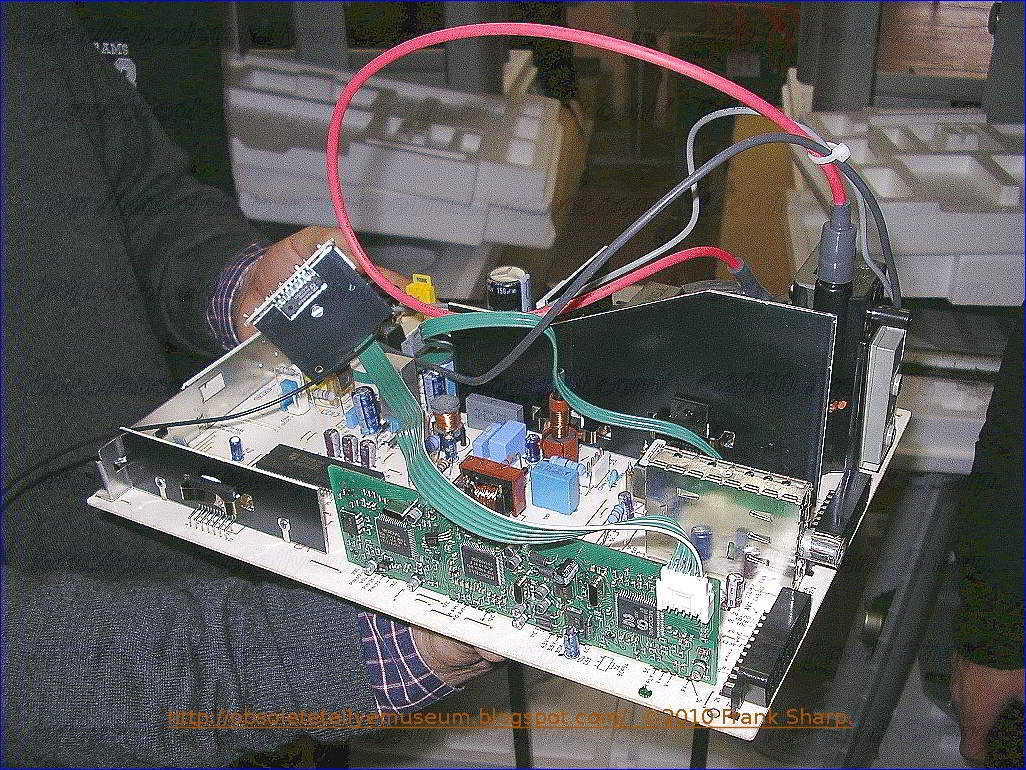


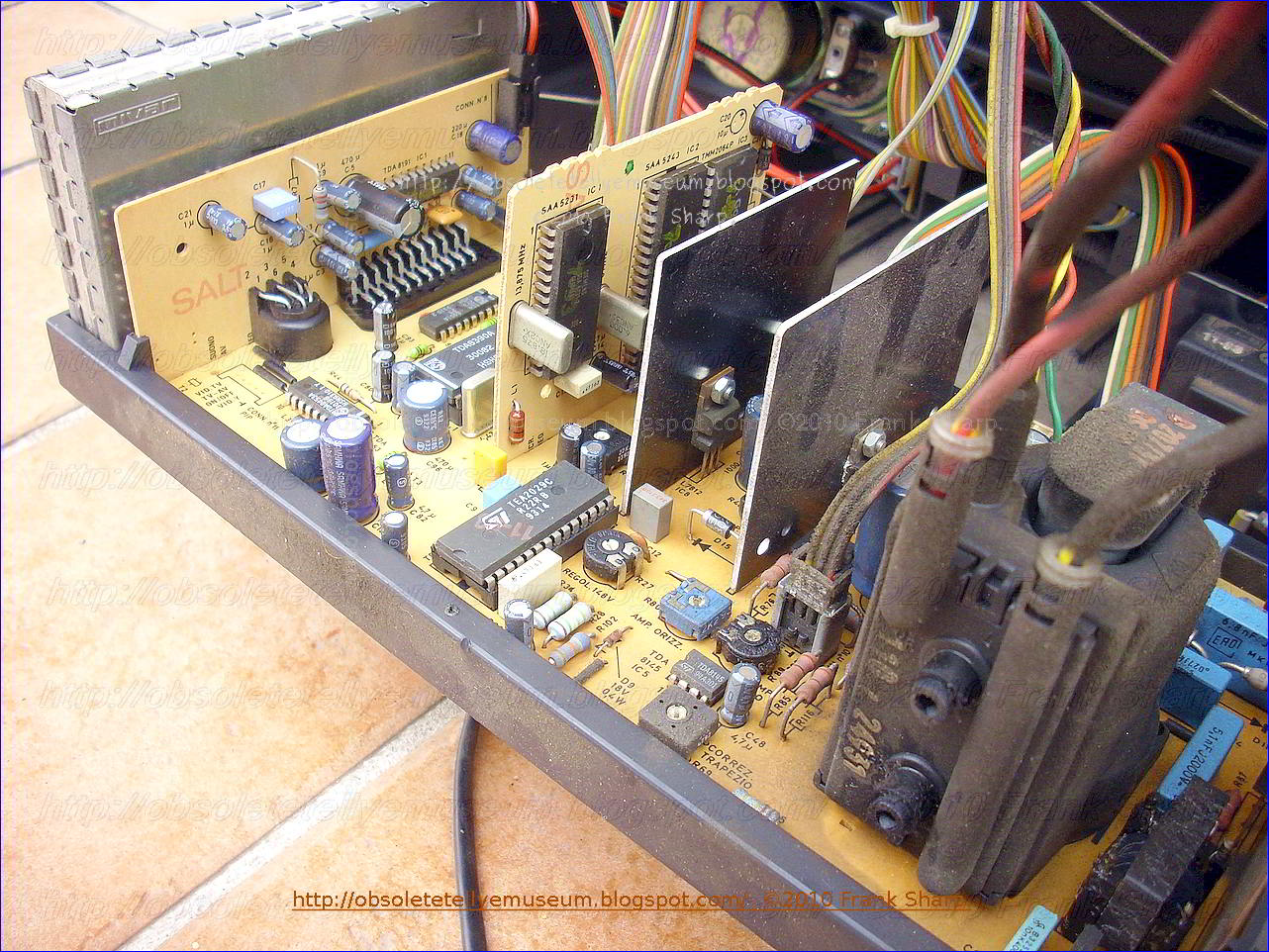


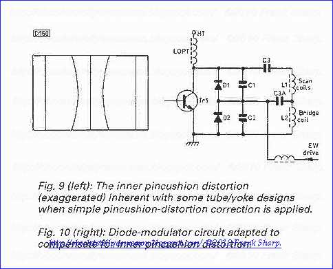


