


The main chassis is a SANYO CHASSIS which was fitted in vary models in that era of time.
The chassis was bought already made and ready to use then fitted in the cabinet with custom controls and frontend.
The tuning and control section is based around ITT SAA1130 and MOTOROLA chipsets.
The tuning search is the MOTOROLA TUNING MEMORY type which was used in varyous Emerson / Dumont and other brands.
SANYO MODEL CTP6240 CHASSIS B5W-62400 Television receiver with an automatic station finding arrangement:
MOTOROLA TUNING MEMORY / MEMOTRONIC SYSTEM TECHNOLOGY.
In a radio or television receiver containing an automatic station finder with a digital counter, a clock generator, and a digital-to-analog converter forming the tuning voltage for the varactors, a recall memory consisting of two series-connected parallel memories is connected in parallel with the digital counter. At a stop signal from the automatic station finder the first parallel memory records the instantaneous count of the digital counter; at an automatic-station-finding start signal the second parallel memory, to which the parallel input of the digital counter is connected, records the contents of the first parallel memory.
1. A receiver having automatic station finding capability, comprising:
means for tuning said receiver in response to an applied voltage;
a controllable pulse generator;
means for starting said pulse generator;
circulating counter means having parallel inputs and outputs, a stepping input and a set input, said stepping input connected to and responsive to pulses from said pulse generator for providing a variable digital output;
digital-to-analog converting means for converting the variable digital output from said counter means to a variable analog voltage, said voltage being applied to said tuning means, so that the receiver is tuned to a frequency corresponding to the analog voltage;
means for sensing a received signal and for providing a stop signal to the pulse generator in response thereto, whereby said generator stops providing pulses and the analog voltage remains constant keeping the receiver tuned to the received signal;
memory means having parallel inputs connected to the parallel outputs of said counter means and parallel outputs connected to the parallel inputs of said counter means;
means associated with said memory means for causing the memory means to store a particular digital output from said counter means; and
means associated with the set input of said counter means for selectively causing the digital signal at the counter input to be transferred to the counter output.
2. A receiver as described in claim 1, wherein the memory means comprises: two series connected parallel memories each having a transfer input, a first of said parallel memories having parallel inputs connected to the parallel outputs of the counter means and having the transfer input connected to the stop signal means, a second of said parallel memories having parallel outputs connected to the parallel inputs of the counter means and having the transfer input connected to the means for starting said pulse generator.
3. A receiver as described in claim 2, wherein each of said parallel memories comprises a plurality of semiconductor voltage flip-flops.
4. A receiver as described in claim 2, wherein the two series connected parallel memories are incorporated in an integrated circuit module with the counter means.
5. A receiver as described in claim 2, wherein the transfer input of the first parallel memory is also connected to the means associated with the set input of the counter means.
6. A receiver as described in claim 1, additionally comprising:
an additional memory means having parallel inputs and outputs;
means for connecting the inputs of said additional memory means to the counter means output and the outputs of said additional memory means to the counter inputs;
means for causing said additional memory means to store a digital output; and
means for transferring the stored digital output to the counter means input through the connecting means.
7. A receiver as described in claim 6, additionally comprising gate means disposed at the outputs of the memory means and the additional memory means for selectively connecting either the additional memory means or the memory means to the input of the counter.
8. A receiver as described in claim 6, wherein the additional memory means comprises a plurality of memories and the connecting means comprises a plurality of station switches corresponding in number to the number of additional memories.
9. A receiver as described in claim 1, wherein each memory means comprises a number of flip-flops corresponding to the number of digits to be stored.
Description:
The present invention relates to a radio or television receiver with an automatic station finding arrangement which contains a pulse generator, a circulating counter formed from semiconductor counting flip-flops and having parallel inputs, a digital-to-analog converter converting the count of the counter to a tuning voltage, and a start-stop circuit acting on the flow of counting pulses and controlled over a start and at least one stop line, and with a parallel memory connected between the parallel outputs and parallel inputs of the counter.
Such a radio receiver is known from, e.g., the journal "Funkschau 1971", pp. 535 to 538 and 587 to 589. With the aid of the free-running pulse generator, the up-counter, and the digital-to-analog converter, the automatic station finding arrangement generates a sawtoothlike tuning voltage for the varactors contained as frequency-setting tuning elements in the resonant circuits of the receiver's radio-frequency portion. If a transmitter is received which meets the receiving criteria set in the receiver, the pulse generator is stopped so that the tuning voltage now remains constant until the operator continues the automatic station finding operation by actuating a start switch.
It is frequently desirable to tune in once again the station at which the start switch for automatic station finding was actuated last - either for comparison or because of the more interesting program. To do this in the case of a receiver with provision for unidirectional automatic station search, the entire search range must be scanned once or several times by repeatedly actuating the start switch, depending on whether the desired station is detected immediately or not.
It is the object of the invention to provide measures for a receiver of the kind referred to by way of introduction which permit the transmitter received before the actuation of the start switch to be found again with a high degree of safety by simple manipulation.
The invention is characterized in that the parallel memory consists of two series-connected parallel memories having one transfer input each, that the transfer input of the (first) parallel memory, whose parallel inputs are connected to the parallel outputs of the counter, are connected directly or indirectly to the stop line, that the transfer input of the (second) parallel memory, whose parallel outputs are connected to the parallel inputs of the counter, is connected directly or indirectly to the start line, that the counter has a set input for through-connecting the parallel inputs of the counter to the flip-flops of the counter, and that a recall switch is connected to the set input of the counter.
Particularly advantageously, the memory locations of the two series-connected parallel memories are storage flip-flops using semiconductor technology. In that case it is possible to arrange the counter and the parallel memories on a common chip of an integrated-circuit module. Such a module has only two terminals more than a module formed by the counter only.
The measures characterized by the invention thus require, aside from an additional recall switch, no additional space and involve nearly no additional expense. To recall the station previously tuned in it is only necessary to depress a button, for example, whereby the receiver is safely tuned to the station's carrier wave even if at the instant of the depression the local received field strength is temporarily too low for sufficient reception.
The invention will now be described in more detail with reference to the accompanying drawing, showing, by way of example, two embodiments of the invention, and wherein:
FIG. 1 is a block diagram showing the radio- and intermediate-frequency portions of a receiver with an automatic station finding arrangement and a recall arrangement;
FIG. 2 shows diagrams a to g explaining the operation of the recall storage, and
FIG. 3 shows a receiver similar to the one of FIG. 1 in which the automatic station finding counter and the recall memories are arranged together on the chip of an integrated-circuit module.
The receivers shown in the block diagrams of FIGS. 1 and 3 have a radio-frequency-receiving section 1, an intermediate-frequency amplif ier 2, and a demodulator section 3, to whose output 4 are connected the arrangements processing the modulation frequency. The tunable resonant circuits of the radio-frequency section contain varactors as tuning elements. Connected to the radio-frequency section is an automatic station finding arrangement in which a digital-to-analog converter 5 generates from the count of a digital counter 7, which receives signals at a stepping input T and advances at the rate of a pulse generator 6, a nearly sawtooth-shaped tuning voltage for the varactors. With a sufficient received field strength at the antenna 8 of the receiver a signal is formed in the demodulator section 3 which signal can be used as stop signal 9 to change the state of a start-stop circuit 10 which may be a flip flop. In the "stop" state the start-stop circuit interrupts the pulse generation or the pulse flow in the pulse generator so that the receiver remains tuned to the station being received. By operating a start-button switch 11 a start signal 12 is generated in the receiver which signal places the start-stop circuit in the "automatic station finding" state and thus continues the automatic station finding operation until next station meeting the receiver's receiving requirements is received.
In the embodiment of FIG. 1, two series-connected parallel memories 15 and 16 are connected, respectively, over two groups of lines 13 and 14 consisting of n lines each, between the n outputs Q 11 to Q n1 and the parallel inputs A 11 to A n1 of the digital counter 7 containing n counting flip-flops. Each parallel memory contains n storage flip-flops and, besides the parallel bit inputs and outputs B and X, a transfer input S. If a transfer signal appears at the transfer input, the parallel memory records the bit word applied its parallel inputs B 1 to B n , which erases the previously entered bit word and now, in turn, appears at the memory outputs X 1 to X n .
The transfer input S of the parallel memory 15, whose parallel inputs are connected over the group of lines 13 to the outputs of the counter 7, is connected to the stop line 17, while the transfer input S of the parallel memory 16, whose parallel outputs are connected over the group of lines 14 to the parallel inputs of the counter 7, is connected to the start line 18.
Connected to a set input P of the digital counters 7 is a switch 19 whose operation generates a set signal. The set signal sets the counter to a count which is equal to the bit word at the parallel inputs A 1 to A n of the counter. At the same time, the set signal acts over the line 20 and via an OR circuit provided for isolation on the transfer input S of the first parallel memory 15.
The diagrams a to g of FIG. 2 explain the operation of the automatic station finding arrangement in conjunction with the recall memories. In diagram a each of the blocks II, III, etc. represents the bit word for a count of the digital counter 7. The blocks in the diagrams b and c are the bit words which are stored in the parallel memories 15 and 16 and can be taken off the latter's parallel outputs, the blocks with equal Roman numerals (e.g. V) representing equal bit words. The diagram d shows the counting pulses 22 for the digital counter 7, the diagram e the stop pulses 9, the diagram f the start pulses 12, and the diagram g the set pulse 23 triggered by the recall switch 19.
The respective count from which the digital-to-analog converter 5 forms the tuning voltage for the varactors is applied simultaneously to the input of the digital-to-analog converter and, as a bit word (e.g. II, III, IV . . . , diagram a), to the input of the first parallel memory 15. At the occurence of a stop signal 9 during the automatic station finding operation, the stop signal 9 acts as a transfer signal on the first parallel memory 15, and the count (e.g. V, diagram a) at which the stop pulse (e.g. 9a) was generated is entered into the first parallel memory 15 (V in diagram b). At the next start pulse 12a triggered via the start-button switch 11 the automatic station finding operation begins anew, starting from the instantaneous count (e.g. V, diagram a) of the counter. The start signal (12a in diagram f) acts as a transfer signal on the transfer input S of the second parallel memory 16, whereby the second parallel memory takes over the bit word (e.g. V) of the first. The next stop signal (e.g. 9b, diagram e) at a new count (e.g. VIII, diagram a) stops the automatic station search and enters the new count as a bit word (e.g. VIII, diagram b) into the first parallel memory 15.
If the operator operates the recall switch 19 so as to recall the setting to the previously received station, the set pulse 23 triggered by the recall switch sets the counter 7 to the count (e.g. V, diagram a) of the bit word (e.g. V, diagram c) stored in the second parallel memory 16, and the newly set count is entered into the first parallel memory 15 (e.g. V, diagram b). The next start signal (e.g. 12b, diagram f) initiates the automatic station finding operation as described.
In the embodiment of FIG. 3, the two series-connected parallel memories 15 and 16 are incorporated on the chip of an integrated-circuit module 25 which also comprises the circulating digital counter 7 and, for exam ple, the circuit 26 of a station memory device. The station memory device has the memory inputs D 1 to D n and the memory outputs Y 1 to Y n of its circuit 26 connected in parallel with the digital counter 7 in the same manner as the recall memory consisting of the two series-connected parallel memories 15 and 16. Therefore, gate circuits 27 and 28 are inserted between the parallel outputs of these memories and the parallel inputs A 1 to A n of the digital counter. The gate circuit 27 between the recall memory and the counter is opened by the set signal of the recall switch 19. The gate circuit 28 between the station memory and the counter is opened by the set signal of a switch 29 for calling the bit word of a station preselected by the station buttons 30. In front of the set input 8 of the digital counter the two set signals are separated from one another in an OR circuit 31.
In the embodiment of FIG. 3, the start-stop circuit 10 is designed in the manner of a flip-flop and can assume a "stop" state and an "automatic station finding" state. The transfer inputs S of the recall memory's parallel memories 15 and 16 are connected via the lines 32 and 33 to the outputs of the start-stop circuit. Since the signals at the outputs of the start-stop circuit are continuous signals, the lines 32 and 33 to the transfer inputs include pulse shapers 34 and 35, respectively.
In embodiments corresponding to FIG. 3 and having no station memory device, besides the circuit 26, the gate circuits 27 and 28 and the OR circuit 31 are omitted.
Such a radio receiver is known from, e.g., the journal "Funkschau 1971", pp. 535 to 538 and 587 to 589. With the aid of the free-running pulse generator, the up-counter, and the digital-to-analog converter, the automatic station finding arrangement generates a sawtoothlike tuning voltage for the varactors contained as frequency-setting tuning elements in the resonant circuits of the receiver's radio-frequency portion. If a transmitter is received which meets the receiving criteria set in the receiver, the pulse generator is stopped so that the tuning voltage now remains constant until the operator continues the automatic station finding operation by actuating a start switch.
It is frequently desirable to tune in once again the station at which the start switch for automatic station finding was actuated last - either for comparison or because of the more interesting program. To do this in the case of a receiver with provision for unidirectional automatic station search, the entire search range must be scanned once or several times by repeatedly actuating the start switch, depending on whether the desired station is detected immediately or not.
It is the object of the invention to provide measures for a receiver of the kind referred to by way of introduction which permit the transmitter received before the actuation of the start switch to be found again with a high degree of safety by simple manipulation.
The invention is characterized in that the parallel memory consists of two series-connected parallel memories having one transfer input each, that the transfer input of the (first) parallel memory, whose parallel inputs are connected to the parallel outputs of the counter, are connected directly or indirectly to the stop line, that the transfer input of the (second) parallel memory, whose parallel outputs are connected to the parallel inputs of the counter, is connected directly or indirectly
to the start line, that the counter has a set input for through-connecting the parallel inputs of the counter to the flip-flops of the counter, and that a recall switch is connected to the set input of the counter. Particularly advantageously, the memory locations of the two series-connected parallel memories are storage flip-flops using semiconductor technology. In that case it is possible to arrange the counter and the parallel memories on a common chip of an integrated-circuit module. Such a module has only two terminals more than a module formed by the counter only.
The measures characterized by the invention thus require, aside from an additional recall switch, no additional space and involve nearly no additional expense. To recall the station previously tuned in it is only necessary to depress a button, for example, whereby the receiver is safely tuned to the station's carrier wave even if at the instant of the depression the local received field strength is temporarily too low for sufficient reception.
The invention will now be described in more detail with reference to the accompanying drawing, showing, by way of example, two embodiments of the invention, and wherein:
FIG. 1 is a block diagram showing the radio- and intermediate-frequency portions of a receiver with an automatic station finding arrangement and a recall arrangement;
FIG. 2 shows diagrams a to g explaining the operation of the recall storage, and
FIG. 3 shows a receiver similar to the one of FIG. 1 in which the automatic station finding counter and the recall memories are arranged together on the chip of an integrated-circuit module.
The receivers shown in the block diagrams of FIGS. 1 and 3 have a radio-frequency-receiving section 1, an intermediate-frequency amplif
 ier 2, and a demodulator section 3, to whose output 4 are connected the arrangements processing the modulation frequency. The tunable resonant circuits of the radio-frequency section contain varactors as tuning elements. Connected to the radio-frequency section is an automatic station finding arrangement in which a digital-to-analog converter 5 generates from the count of a digital counter 7, which receives signals at a stepping input T and advances at the rate of a pulse generator 6, a nearly sawtooth-shaped tuning voltage for the varactors. With a sufficient received field strength at the antenna 8 of the receiver a signal is formed in the demodulator section 3 which signal can be used as stop signal 9 to change the state of a start-stop circuit 10 which may be a flip flop. In the "stop" state the start-stop circuit interrupts the pulse generation or the pulse flow in the pulse generator so that the receiver remains tuned to the station being received. By operating a start-button switch 11 a start signal 12 is generated in the receiver which signal places the start-stop circuit in the "automatic station finding" state and thus continues the automatic station finding operation until next station meeting the receiver's receiving requirements is received.
 In the embodiment of FIG. 1, two series-connected parallel memories 15 and 16 are connected, respectively, over two groups of lines 13 and 14 consisting of n lines each, between the n outputs Q 11 to Q n1 and the parallel inputs A 11 to A n1 of the digital counter 7 containing n counting flip-flops. Each parallel memory contains n storage flip-flops and, besides the parallel bit inputs and outputs B and X, a transfer input S. If a transfer signal appears at the transfer input, the parallel memory records the bit word applied its parallel inputs B 1 to B n , which erases the previously entered bit word and now, in turn, appears at the memory outputs X 1 to X n .
The transfer input S of the parallel memory 15, whose parallel inputs are connected over the group of lines 13 to the outputs of the counter 7, is connected to the stop line 17, while the transfer input S of the parallel memory 16, whose parallel outputs are connected over the group of lines 14 to the parallel inputs of the counter 7, is connected to the start line 18.
Connected to a set input P of the digital counters 7 is a switch 19 whose operation generates a set signal. The set signal sets the counter to a count which is equal to the bit word at the parallel inputs A 1 to A n of the counter. At the same time, the set signal acts over the line 20 and via an OR circuit provided for isolation on the transfer input S of the first parallel memory 15.
The diagrams a to g of FIG. 2 explain the operation of the automatic station finding arrangement in conjunction with the recall memories. In diagram a each of the blocks II, III, etc. represents the bit word for a count of the digital counter 7. The blocks in the diagrams b and c are the bit words which are stored in the parallel memories 15 and 16 and can be taken off the latter's parallel outputs, the blocks with equal Roman numerals (e.g. V) representing equal bit words. The diagram d shows the counting pulses 22 for the digital counter 7, the diagram e the stop pulses 9, the diagram f the start pulses 12, and the diagram g the set pulse 23 triggered by the recall switch 19.
The respective count from which the digital-to-analog converter 5 forms the tuning voltage for the varactors is applied simultaneously to the input of the digital-to-analog converter and, as a bit word (e.g. II, III, IV . . . , diagram a), to the input of the first parallel memory 15. At the occurence of a
stop signal 9 during the automatic station finding operation, the stop signal 9 acts as a transfer signal on the first parallel memory 15, and the count (e.g. V, diagram a) at which the stop pulse (e.g. 9a) was generated is entered into the first parallel memory 15 (V in diagram b). At the next start pulse 12a triggered via the start-button switch 11 the automatic station finding operation begins anew, starting from the instantaneous count (e.g. V, diagram a) of the counter. The start signal (12a in diagram f) acts as a transfer signal on the transfer input S of the second parallel memory 16, whereby the second parallel memory takes over the bit word (e.g. V) of the first. The next stop signal (e.g. 9b, diagram e) at a new count (e.g. VIII, diagram a) stops the automatic station search and enters the new count as a bit word (e.g. VIII, diagram b) into the first parallel memory 15. If the operator operates the recall switch 19 so as to recall the setting to the previously received station, the set pulse 23 triggered by the recall switch sets the counter 7 to the count (e.g. V, diagram a) of the bit word (e.g. V, diagram c) stored in the second parallel memory 16, and the newly set count is entered into the first parallel memory 15 (e.g. V, diagram b). The next start signal (e.g. 12b, diagram f) initiates the automatic station finding operation as described.
In the embodiment of FIG. 3, the two series-connected parallel memories 15 and 16 are incorporated on the chip of an integrated-circuit module 25 which also comprises the circulating digital counter 7 and, for exam
 ple, the circuit 26 of a station memory device. The station memory device has the memory inputs D 1 to D n and the memory outputs Y 1 to Y n of its circuit 26 connected in parallel with the digital counter 7 in the same manner as the recall memory consisting of the two series-connected parallel memories 15 and 16. Therefore, gate circuits 27 and 28 are inserted between the parallel outputs of these memories and the parallel inputs A 1 to A n of the digital counter. The gate circuit 27 between the recall memory and the counter is opened by the set signal of the recall switch 19. The gate circuit 28 between the station memory and the counter is opened by the set signal of a switch 29 for calling the bit word of a station preselected by the station buttons 30. In front of the set input 8 of the digital counter the two set signals are separated from one another in an OR circuit 31.
 In the embodiment of FIG. 3, the start-stop circuit 10 is designed in the manner of a flip-flop and can assume a "stop" state and an "automatic station finding" state. The transfer inputs S of the recall memory's parallel memories 15 and 16 are connected via the lines 32 and 33 to the outputs of the start-stop circuit. Since the signals at the outputs of the start-stop circuit are continuous signals, the lines 32 and 33 to the transfer inputs include pulse shapers 34 and 35, respectively.
In embodiments corresponding to FIG. 3 and having no station memory device, besides the circuit 26, the gate circuits 27 and 28 and the OR circuit 31 are omitted.
Tuning Search + Drive
Employs the Motorola Tuning Memory System.
a complex circuitry with mixed signals technology.
- UAA1008 (Tuning Drive + AFC + D/A)
- MC14426 (Memory )
- MC14429 (MEMORY SYSCON)
SANYO MODEL CTP6240 CHASSIS B5W-6240 Vertical deflection circuit:
A vertical deflection circuit for use in a television receiver, comprising a control circuit for stabilizing the width of a  pulse either in a vertical oscillator circuit or between a vertical oscillator circuit and vertical output circuit to thereby stabilize the width of a pulse component included in the vertical deflection output signal.
pulse either in a vertical oscillator circuit or between a vertical oscillator circuit and vertical output circuit to thereby stabilize the width of a pulse component included in the vertical deflection output signal. 1. A transformerless output vertical deflection circuit, comprising a vertical oscillator circuit for generating a vertical pulse train in response to vertical synchronizing pulses applied thereto, a sawtooth signal generator for generating a series of sawtooth signals, each cycle of said sawtooth signal including a pulse component, a vertical output circuit coupled to said sawtooth generator for amplifying said sawtooth signal including said pulse component and loading a vertical deflection coil, and stabilizing means connected between said vertical oscillator and said sawtooth signal generator for varying the width of the pulse component which is to be fed to said vertical output circuit in response to the average level of DC output voltage fed from the vertical output circuit.
2. A transformerless output vertical deflection circuit claimed in claim 1, wherein said stabilizing means comprises a control circuit means for receiving a series of pulses from the vertical oscillator and a feedback signal from the vertical output circuit and for varying the width of the pulse which is to be fed to the vertical output circuit in response to a DC control signal proportional to the width of the pulse component included in the vertical output signal and smoothing circuit means connected between said vertical output circuit and said stabalizing means for smoothing said feedback signal.
3. A transformerless output vertical deflection circuit claimed in claim 2, wherein said control circuit comprises a charging capacitor which is parallel to a transistor, said transistor being switched on in response to pulses fed from the vertical oscillator wherein said capacitor is charged by the voltage fed from said smoothing circuit, and discharged in response to conduction of the transistor, a differential amplifier circuit which receives the voltage on said capacitor and a fixed voltage, and a gating circuit for producing a pulse which has a width equal to the difference between the width of the pulse fed from the vertical oscillator circuit and the width of pulse fed from the differential amplifier circuit.
4. A transformerless output vertical deflection circuit claimed in claim 2, wherein said control circuit comprises a capacitor which is charged by a fixed power source and is discharged by means of a switching transistor operated by the pulses fed from the vertical oscillator circuit and a differential amplifier circuit receiving the voltage on the capacitor and the output of said smoothing circuit.
5. A transformable output vertical deflection cir
cuit comprising a vertical oscillator for generating a vertical pulse train in response to vertical synchronizing pulses applied thereto, a sawtooth signal generator for generating a series of sawtooth signals each cycle of said sawtooth signal including a pulse component, a vertical output circuit for amplifying said sawtooth signal including said pulse component and loading a vertical deflection coil, and pulse stabilizing means coupled between the vertical oscillator circuit and the sawtooth signal generator, said stabilizing means comprising a capacitor which is charged by a fixed power source and discharged by means of a discharging means operated in response to the vertical pulse fed from the vertical oscillator, a circuit means for generating a train of output pulses each starting at the time when the voltage appearing on the capacitor exceeds a predetermined value and terminating in synchronism with termination of the pulse fed from the vertical oscillator, and gating means for generating pulses having a width equal to the difference between the width of the pulse fed from the vertical oscillator and the width of the output pulse of the circuit means. 6. A transformerless output vertical deflection circuit, comprising a vertical oscillator circuit for generating a vertical pulse train in response to vertical synchronizing pulses applied thereto, a sawtooth signal generator for generating a series of sawtooth signals, each cycle of said sawtooth signal including a pulse component, a vertical output circuit coupled to said sawtooth generator for amplifying said sawtooth signal including said pulse component and loading a vertical deflection coil, and stabilizing means, comprising a control circuit connected between said vertical output circuit and said vertical oscillator circuit for varying the width of each pulse produced by the vertical oscillator circuit in response to a DC control signal having a value corresponding to the width of the pulse component applied to the vertical deflection coil of the vertical output circuit for controlling the pulse width of the output of said vertical oscillator circuit and thereby the pulse width of said pulse component.
Description:
BACKGROUND OF THE INVENTION
The present invention relates to a vertical deflection circuit for use in a television receiver and, more particularly, to a vertical deflection circuit of a type wherein no vertical output transformer is employed. This type of vertical deflection circuit with no output transformer is generally referred to as an OTL (Output Transformerless) type vertical deflection circuit.
It is known that variation of the pulse width of the flyback pulse produced in a vertical output stage of the vertical deflection circuit is the cause in the raster on the television picture tube, of a white bar, flicker, jitter, line crowding and/or other raster disorders. In addition thereto, in the vertical deflection output circuit where the output stage is composed of a single-ended push-pull amplifier having a vertical output transistor, an excessive load is often imposed on the output transistor and, in an extreme case, the output transistor is destroyed.
One of the major causes for variation of the vertical flyback pulse width is interference by horizontal flyback pulses from the horizontal deflection circuit, in which case sufficient interlaced scanning can not be performed.
In order to avoid these inconveniences, the vertical flyback pulse width must be controlled at a constant width. However, by the reason as will be described with reference to FIG. 1, a prior art vertical deflection circuit in a television receiver fails to satisfy this requirement.
Referring now to FIG. 1 wherein a prior art vertical deflection circuit now under discussion is shown, a circuit arrangement is such that synchronizing pulses emerging from a sync separator 1 are, after having its waveform shaped in an integrator 2, applied to a vertical oscillating circuit 3 which includes a vertical oscillator 4 and a sawtooth deflecting signal generator 5. The vertical oscillator 4 upon receipt of the shaped sync pulses from the integrator 2 is driven to generate a train of pulses synchronized with the vertical synchronizing signal which are subsequently fed to the sawtooth deflecting signal generator 5. The waveform of a sawtooth deflecting signal emerging from the generator 5 is shown in FIG. 2 and this deflecting signal is transferred from the generator 5 to a vertical deflection output circuit 6 which includes a drive circuit 7 for amplifying the sawtooth deflecting signal upon receipt thereof from the generator 5 and a vertical output stage 8 having a vertical deflection coil D.
As shown in FIG. 2, the sawtooth deflecting signal includes rectangular component pulses and the wave-form of an output signal from the vertical output stage 8 which is similar to that of the sawtooth deflecting signal. The portions of the output signal from the vertical output stage 8, which correspond to the rectangular component pulses of the sawtooth deflecting signal are known as flyback pulses.
In the vertical deflection circuit of the above arrangement, the pulse width of the flyback pulses included in the output of the vertical output stage 8 is affected by the pulse width of the rectangular component pulses fed from the oscillator 4 to the output stage 8. More specifically, in the OTL type vertical deflection circuit, since there is no inductance element, such as a vertical output transformer, that determines the pulse width of the flyback pulse, the pulse width of the flyback pulse is mostly determined by the pulse width of the corresponding rectangular component pulse of the sawtooth deflecting signal applied to the output stage 8. Accordingly, variation of the pulse width of the rectangular component pulses produced in the oscillator 4 results in variation of the pulse width of the flyback pulses produced in the output stage 8.
This inconvenience is likely to be avoided if the pulse width of the output pulse from the oscillator 4 is stabilized. However, this stabilization of the pulse width of the output pulse from the oscillator 4 cannot be achieved without difficulties by the following reason.
In the vertical oscillator 4, the start of each output pulse from this oscillator 4 can be accurately determined by the vertical synchronizing signal applied thereto. On the contrary thereto, the time at which the output pulse from the oscillator 4 terminates is solely determined by operational characteristics of the oscillator 4 itself and, therefore, is often adversely affected by and in the presence of external noises. Once the oscillator 4 is adversely affected by and in the presence of the external noises, the duration between the start and termination of the output pulse from said oscillator, that is, the pulse width, varies and, therefore, the problem remains still unsolved.
SUMMARY OF THE INVENTION
Accordingly, an essential object of the present invention is to provide a vertical deflection circuit for use in a television receiver, which substantially eliminates the inconveniences inherent in the conventional circuit of a similar kind and which effectively stabilizes the pulse width of flyback pulses included in a vertical deflection output signal.
Another important object of the present invention is to provide a vertical deflection circuit of the type referred to above, wherein a pulse width control is provided between the vertical oscillator and the vertical output circuit for controlling the pulse width of the output pulses from the oscillator.
A further important object of the present invention is to provide a vertical deflection circuit of the type referred to above, wherein a feedback loop is provided to control the operation of the pulse width control in response to an output signal emerging from the vertical output stage.
A still further important object of the present invention is to provide a vertical deflection circuit of the type referred to above, wherein a feedback loop is provided to control the oscillator in response to an output signal emerging from the vertical output stage for stabilizing the pulse width of the flyback pulses produced in the vertical output stage.
These and other objects and features of the present invention will become clear from the following description taken in conjunction with preferred embodiments of the present invention with reference to the accompanying drawings in which;
BRIEF DESCRIPTION OF THE DRAWINGS
FIG. 1 is a block diagram showing the prior art vertical deflection circuit,
FIG. 2 is a diagram showing the waveform of vertical deflection output produced in the prior art vertical deflection circuit,
FIG. 3 is a block diagram showing one embodiment of the vertical deflection circuit according to the present invention,
FIG. 4 is a circuit diagram showing the details of the vertical deflection circuit shown in FIG. 3,
FIG. 5 is a diagram showing waveforms of various signals obtainable at various portions of the circuit of FIG. 4.
FIG. 6 is a block diagram showing another embodiment of the vertical deflction circuit according to the present invention,
FIG. 7 is a circuit diagram showing the details of the vertical deflection circuit shown in FIG. 6,
FIG. 8 is a diagram showing waveforms of various signals obtainable at various portions of the circuit of FIG. 7,
FIG. 9 is a circuit diagram showing a further embodiment of the vertical deflection circuit according to the present invention,
FIG. 10 is a diagram showing waveforms of various signals obtainable at various portions of the circuit of FIG. 9.
FIG. 11 is a block diagram showing a still further embodiment of the vertical deflection circuit according to the present invention,
FIG. 12 is a circuit diagram showing the details of the vertical deflection circuit shown in FIG. 11, and
FIG. 13 is a diagram showing waveforms of various signals obtainable at various portions of the circuit of FIG. 12.
Before the description of the present invention proceeds, it should be noted that like parts are designated by like reference numerals throughout the accompanying drawings for the sake of brevity.
DESCRIPTION OF THE PREFERRED EMBODIMENTS
 Referring now to FIG. 3, between the vertical oscillator 4 and the sawtooth deflecting signal generator 5, there is provided a pulse width control circuit 9 for stabilizing the pulse width of pulses fed to the sawtooth deflecting signal generator 5 from the vertical oscillator 4.
FIG. 4 shows details of the pulse width control circuit 9, which will now be described.
Assuming that a pulse of unstable pulse width is applied from the vertical oscillator 4 to the input terminal T1 of the pulse width control circuit 9, which is in turn applied to the base of a switching transistor Tr1, the latter is triggered on to cause the capacitor C1 to discharge. In other words, when the pulse is applied to the pulse width control circuit 9 from the oscillator 4, that is, when the switching transistor Tr1 is non-conductive, voltage from the D-C power source Vb, after having passed through the resistor of sufficiently high resistance, charges the capacitor C1. However, the charge stored in the capacitor C1 is discharged to the ground through the collector-emitter of the switching transistor Tr1 when the latter starts conducting.
 As a result, in the capacitor C1, voltage of sawtooth waveform as shown by the solid line in FIG. 5(b) is generated across said capacitor C1, which is subsequently applied to the base of a switching transistor Tr2. The latter transistor Tr2 starts conducting only when the voltage thus applied to the base thereof exceeds a D-C power source voltage E1 applied to the emitter of said transistor Tr2. Conduction of the switching transistor Tr2 results in a pulsating voltage of rectangular waveform, as shown by the solid line in FIG. 5(c), appearing at the common junction J1 of resistors R2 and R3, both of which are loaded on the collector of the transistor Tr2, due to the saturation characteristic of the transistor Tr2. The pulsating voltage at the common junction J1 is fed to the base of an amplifying transistor Tr3 so that the pulsating voltage is thereby amplified and phase-reversed and, as a result thereof, a phase-reversed pulsating voltage of the waveform as shown by the solid line in FIG. 5(d) appears at the common junction J2 of resistors R4 and R5, both of which are loaded on the collector of the transistor Tr3. This pulsating voltage at the common junction J2 is further phase-reversed by an amplifying transistor Tr4. Therefore, a voltage received by the transistor Tr6 from the collector of the amplifying transistor Tr4 has a waveform similar to that of the pulsating voltage applied to the base of the amplifying transistor Tr3.
Simultaneously, the output pulse at the input terminal T1 is also applied to the base of a transistor Tr5. The transistor Tr5 acts to phase-reverse the output pulse to produce a pulsating voltage of a waveform as shown by the solid line in FIG. 5(e) at the collector of said transistor Tr5. The collector of this transistor Tr5 is connected with the collector of the transistor Tr4, which is in turn connected to the base of the transistor Tr6. This transistor Tr5 is non-conductive when voltage applied to the base threof is zero, in which condition the base of the transistor Tr6 receives a pulse of positive potential, i.e., a high level pulse, whereby it is held in a conductive state with the collector thereof in a zero volt or low level state. If the high level pulse is applied to the base of the transistor Tr4, this high level pulse is amplified and phasereversed by the transistor Tr4 toproduce a low level pulse from the collector thereof which is in turn fed to the transistor Tr6 to trigger the latter off. When the transistor Tr6 is thus triggered off, a high level voltage is produced from the collector of the transistor Tr6.
In view of the foregoing, it can be seen that these transistors Tr4, Tr5 and Tr6 cooperate with each other to substantially act as a gating circuit while the pulsating voltage applied to the base of the transistor Tr6 from the transistor Tr4 acts as a trigger pulse. Accordingly, it is clear that the pulse appearing at the collector of the transistor Tr6 has a pulse width, as shown in FIG. 5(f), which corresponds to the pulse width W1 of the output pulse at the input terminal T1 extracted by the pulse width W2 of the high level pulse applied to the base of the transistor Tr4.
As stated hereinbefore, the start of the output pulse from the oscillator 4 can be accurately fixed while it is difficult to fix the termination of the pulse. Assuming, therefore, that the output pulse shown by the broken line in FIG. 5(a) and having a pulse width t1 to t4 which is larger than the desired pulse width t1 to t2 as shown by the solid line in FIG. 5(a), is applied to the pulse width control circuit 9 from the vertical oscillator 4, the transistor Tr1 becomes non-conductive and the voltage across the capacitor C1 accordingly increases as shown by the broken line in FIG. 5(b). On the other hand, the transistor Tr5 becomes non-conductive upon receiving of the input pulse at the base thereof at the time t1, causing the transistor Tr6 to start conducting.
When the voltage at the base of the transistor Tr2 exceeds the emitter voltage defined by the source E1, the transistors Tr2 and Tr3 become conductive and the junction point J2 becomes high level at the time t3 as shown in FIG. 5(d). Accordingly, the collector of the transistor Tr4 becomes low level causing the transistor Tr6 to become non-conductive whereby the collector of the transistor Tr6 becomes high level at the time t3.
From the foregoing, it is clear that, even if the width of the input pulse applied to the pulse width control circuit 9 is larger than the desired or predetermined width, the width output pulse of the control circuit 9 can be defined at the predetermined width as shown in FIG. 5(f).
Accordingly, a rectangular pulse having a predetermined pulse width is applied to the base of the input transistor Tr8 of the sawtooth signal generator 5, whereby the width of the flyback pulses included in the vertical deflection output can be maintained at the desired or predetermined width.
In the embodiment of FIG. 3, the pulse width of the output pulse of the pulse width control circuit 9 may not be suitable for the vertical output circuit. In this case, equalization of the pulse width can be achieved by varying the D-C voltage E1 supplied to the emitter of the transistor Tr2. Specifically, if the voltage E1 increases or decreases the pulse width at the output terminal F of the control circuit 9 is reduced or enlarged, respectively.
FIG. 6 shows another embodiment of the present invention in which the pulse width control circuit 9' receives a feedback signal from the deflection output circuit 8 so that the pulse width of the output signal from the width control circuit 9' can be advantageously controlled to maintain the width of the flyback pulse constant.
FIG. 7 shows the details of the width control circuit 9'. Referring now to FIG. 7, there is provided a differential amplifier 10 composed of transistors Tr13 and Tr14. The base of the transistor Tr13 receives the voltage on the capacitor C1 and feedback voltage fed back from the common junction J6 of the deflection output circuit through the integrator 11 and the resistors R5 and R6.
 The collector of the transistor Tr13 is connected to the base of the transistor Tr4 which constitutes the gating circuit in cooperation with the transistors Tr5 and Tr6. The switching level of the transistor Tr13 is defined by base voltage Eo appearing at the junction point J3 of the resistors R7 and R8.
Operation of the circuit arrangement of FIGS. 6 and 7 will now be described.
It is assumed that, during operation of the control circuit 9' with the transistor Tr1 triggered off by the application of the low level pulse from the vertical oscillator 4, voltage supplied from the integrator 11 through the constant current resistor R5 and then a time constant adjusting resistor R6 charges the capacitor C1. Voltage of a sawtooth waveform as shown by the solid line in FIG. 8(b) is generated across the capacitor C1. This sawtooth voltage is subsequently fed to the differential amplifier 10. The charging speed of the capacitor C1 is defined by the voltage E F of the integrator 11.
When the voltage at the base of the transistor Tr13 exceeds the voltage Eo appearing at the base of the transistor Tr14, the transistor Tr13 becomes conductive with the output of the transistor Tr13 becoming low level. At the end of the input pulse, transistor Tr1 becomes conductive, the capacitor C1 is discharged, whereby the transistor Tr13 becomes non-conductive causing the output of the transistor Tr13 to become high level.
Therefore, pulses of rectangular waveform as shown by the solid line in FIG. 8(c) can be generated from the collector of the transistor Tr13. The pulses from the transistor Tr13 are amplified and phase-reversed by the transistor Tr4, which are in turn applied to the base of the transistor Tr7 through the transistor Tr5. It should be noted that the waveform of pulse at the junction J5 between the transistors Tr4 and Tr5 is shown by the solid lines in FIG. 8(d).
Simultaneously, the pulses from the input terminal T1 are also applied to the base of the transistor Tr6. Consequently, in a similar manner as in the circuit arrangement of FIG. 4, pulses of a waveform as shown by the solid line in FIG. 8(f) can be obtained at the collector of the transistor Tr7 and, hence, at the output terminal T2 of the width control circuit 9'.
The output pulses from the width control circuit 9' are supplied to the base of the transistor Tr9 through the transistor Tr8, said transistors Tr8 and Tr9 forming the sawtooth signal generator 5. Output from the sawtooth signal generator 5 is then applied to the base of the transistor Tr10 in the form of sawtooth pulses as shown, thereby causing the transistor Tr10 to generate trigger pulse for driving the vertical output transistors Tr11 and Tr12 in the known manner. The result is that vertical deflection output of a waveform as shown by the solid line in FIG. 8(g) appears at the junction J6 from which it is applied in part to the vertical deflection coil D and in part to the resistor R5 through the feedback loop. The deflection output that has been fed through the feedback loop is, prior to application thereof to the resistor R5, smoothed by the integrator 11 which is composed of the resistor R9 and the capacitor C2, to obtain a control voltage Ef of a suitably divided value.
Assuming that the pulse width Pr of flyback pulses included in the vertical deflection output from the vertical output stage 8 varies, for example, gets smaller and is at a value Pr', the voltage Vr of the flyback pulse accordingly increases by the reason of the following equation: ##EQU1## wherein L is inductance of the vertical deflection coil D, i is vertical deflection current and K is a constant. In other words, while the peak level C of the flyback pulse is determined by the D-C power source voltage Vb2 and, therefore, does not vary, the average D-C voltage level Vm of the vertical deflection output is lowered to read a value Vm' as shown in FIG. 8(g).
Consequently, the pulse width control voltage Ef applied to the resistor R5 through the integrator 11 is lowered and the voltage to which the capacitor C1 is charged is also lowered. The result is such that, as indicated by the broken line in FIG. 8(b), the charging speed of the capacitor C1 is retarded whereby conduction of the transistor Tr13 is delayed. Accordingly, the waveforms of the pulses P1 and P2 at the junctions J4 and J5 are respectively narrowed as shown by the broken lines in FIG. 8(c) and (d). As a result thereof, the pulse width of the output pulse appearing at the output terminal T2 of the width control circuit 9' is broadened as shown by the broken line in FIG. 8(f) since the width of the pulse appearing at the terminal T2 is defined by a difference between the pulse at the base of the transistor Tr6 and the pulse at the base of the transistor Tr5. Therefore, the variation of the pulse width Pr of the vertical flyback pulse can be advantageously and effectively compensated for.
 FIG. 9 shows a further embodiment of the present invention. In the circuit arrangement of FIG. 9, the output from the oscillator 4 is first applied to the amplifying transistor Tr15 by which it is amplified and phase-reversed. From this transistor Tr15, the pulse of a waveform as shown in FIG. 10(a) is applied to the base of the transistor Pr1, thereby causing the latter to be triggered on. During a period in which the transistor Tr1 is non-conductive, the capacitor C1 is charged through the constant current transistor Tr16 and, when the transistor Tr1 starts conducting upon receipt of the pulse from the transistor Tr15, voltage charged in the capacitor C1 is discharged through the collector-emitter of the transistor Tr1. By this operation, voltage of the sawtooth waveform as shown in FIG. 10(b) is generated across the capacitor C1. This sawtooth voltage is subsequently applied to a differential amplifier 10 composed of a pair of transistors Tr13 and Tr14. The transistor Tr14 receives control voltage Ef fed from the junction point J6 of the vertical deflection output stage 8 through the integrator 11. By the level Ef of voltage fed to the base of the transistor Tr14, the slicing level of this sawtooth voltage can be varied and, hence, the pulse width of the pulse emerging from the collector of the transistor Tr14 can be varied as indicated by W1 in FIG. 10(c). The output pulse from the collector of the transistor Tr14 is fed to the base of the transistor Tr10 of the drive circuit 7 through the sawtooth signal generator 5. The vertical deflection output of a waveform as shown in FIG. 10(d) is generated at the junction J6 of the vertical output stage 8 after the output transistors Tr11 and Tr12 are driven by drive signal from the drive circuit 7.
Assuming now that the pulse width W of the output from the oscillator 4 is suitably selected such as to be larger than that required in the vertical deflection output from the output stage 8, if the flyback pulse width Tr of the vertical deflection output becomes larger than the pulse width W, the voltage Vr of the flyback pulse is reduced for the same reason as in the embodiment of FIG. 7 while the peak level C thereof remains the same and, accordingly, the average D-C voltage Vm increases, resulting in increase of the control voltage Ef to be applied to the base of the transistor Tr14.
Therefore, the slicing level of the sawtooth voltage determined by the differential amplifier increases as indicated by the broken line in FIG. 10(b) and the pulse width of the output pulse emerging from the collector of the transistor Tr14 is reduced.
In this way, variation of the output pulse from the oscillator 4 resulting from the variation of the oscillator 4 itself can be advantageously and adequately compensated for by the control circuit 9' and the average D-C voltage Vm of output from the output stage 8 and the flyback pulse of the vertical deflection output are respectively controlled to assume a predertermined value.
FIG. 11 shows a still further embodiment of the present invention in which feedback voltage fed from the vertical output stage 8 is applied to the vertical oscillator 4 to maintain the width of the output pulse of the vertical oscillator 4 at a constant value.
The detailed circuit of the vertical oscillator 4 is shown in FIG. 12.
Referring to FIG. 12, the output pulse of the integrator 2 is applied to a base of a transistor Tr21 the collector of which is connected to the base of a transistor Tr22 through a resistor R21. The transistor Tr22 constitutes the differential amplifier in cooperation with a transistor Tr23 the base of which is connected to a capacitor C3 receiving voltage E1 of the D-C power source through a variable resistor VR.
The collector of the transistor Tr23 is connected to the base of an amplifying transistor Tr24 of which the collector is connected to the base of a transistor Tr25 through resistors R24 and R25. The collector of the transistor Tr25 is applied to the base of a transistor Tr26 and collector of a transistor Tr27 through a transistor Tr28. The junction point of the collector Tr27 and the base of the transistor Tr26 is grounded through a resistor R26 and a diode D1. The transistor Tr27 operates as a current stabilizer which is controlled by the collector output of the transistor Tr29. The transistor Tr27 receives control voltage Ec which is fed from the integrator 11 through a transistor Tr29. The collector output of the transistor Tr25 is applied to the base of the transistor Tr8 in the sawtooth signal generator 5.
Operation of the vertical deflection circuit shown in FIG. 12 will now be described.
Assuming that a main switch (not shown) for connection between the circuit and a power source (not shown) is turned on and a capacitor C3 of the oscillator 4, is not charged no voltage is applied to the base of the transistor Tr23 which forms the differential amplifier. During this condition, that is, when the base voltage Vb1 of the transistor Tr23 is zero, the transistor Tr23 is non-conductive while the collector voltage thereof is high and, therefore, a transistor Tr24 is non-conductive. Likewisely, the transistors Tr21 and Tr25 have not yet been switched on and, accordingly, a transistor Tr28 is conductive. The switching transistor Tr26 for generation of sawtooth voltage is at this time non-conductive.
During a period in which the transistor Tr21 is non-conductive, the base voltage Vb2 applied to the base of the transistor Tr22 is represented by the following equation: ##EQU2## wherein r21, r23 and r24 are resistances of the resistors R21, R22 and R23, respectively and E1 is the D-C power source voltage.
Subsequent switching on of the main switch permits the D-C power source voltage E1 to charge the capacitor C3 through the oscillation frequency adjusting resistor VR in such a manner as shown in FIG. 5(b). When the base voltage Vb1 of the transistor Tr23 starts to exceed the base voltage Vb2 of the transistor Tr22 at the time t1 a predetermined time after the capacitor C3 has been charged, the transistors Tr23 and Tr22 are respectively triggered on and off. Upon conduction of the transistor Tr23, the transistors Tr21 and Tr25 start conducting. Conduction of the transistor Tr25 results in reduction of the collector voltage thereof and, therefore, the transistor Tr28 is triggered off.
As the transistor Tr28 becomes non-conductive, the collector voltage of the transistor Tr28 increases, thereby triggering the transistor Tr26 on so that the charge on the capacitor C3 is discharged through the collector-emitter of the transistor Tr26. At this time, the collector current of the transistor Tr26 (i.e., the current flowing through the capacitor C3) is made to be constant by a constant current circuit which is composed of the transistor Tr27 and a diode D1. During this condition, the transistor Tr21 is conductive and, therefore, the base voltage Vb2 of the transistor Tr22 is lowered as represented by the following equation: ##EQU3##
Accodingly, discharge of the potential stored in the capacitor C3 continues at a constant current determined by the base potential of the transistor Tr27 until the base voltage Vb1 of the transistor Tr23 becomes equal to the base voltage ##EQU4## of the transistor Tr22 at the time t2. Thereafter, the transistor Tr23 is again triggered off while the transistor Tr22 is triggered on and this operation is repeated. The result is such that pulses of a rectangular waveform as shown in FIG. 13(e) are generated through the collector J9 of the transistor Tr25. The waveform of output pulse apearing at the output terminal T1 of the integrator 2 is as shown in FIG. 13(a) and this vertical synchronizing pulse is applied to the base of the transistor Tr21 whereby the oscillator 4 is oscillated in synchronizm with said vertical synchronizing pulses.
Waveforms of signals at the junctions J7, J8 and J6 are shown in FIGS. 13(c), (d) and (f), respectively.
On the other hand, though the start time t1 (FIG. 13(e )) of the output pulse from the oscillator 4 can be accurately determined because of synchronization with the vertical synchronizing pulse from the integrator 2, the termination t2 thereof cannot be accurately determined by the reason as hereinbefore described. If the pulse width of the output pulse from the oscillator 4 varies to represent a pulse width between t1 and t2' short of the required pulse width and the output pulse having such a reduced width is applied to the sawtooth signal generator 5 from the oscillator 4 the flyback pulse width Pr of the vertical deflection output at the junction J6 of the vertical output stage 8 is consequently reduced to a value Pr' as shown by the broken line in FIG. 13(f). The result is that the voltage Vr of the flyback pulse increases to represent a value Vr' by the reason as hereinbefore described in connection with the equation (1).
A voltage proportional to the average level Vm of D-C output voltage is extracted from a smoothing circuit 11, which is composed of the resistor R9and a capacitor C4, and is subsequently fed to a transistor Tr29 for D-C amplification and phase-reversion. The transistor Tr29, upon receipt of this voltage from the smoothening circuit 11, generates voltage from the collector thereof which is used as a pulse width control voltage Ec which is subsequently applied to the base of the transistor Tr27. It is to be noted that the control voltage Ec increases in response to reduction of the flyback pulse width and, accordingly, the emitter-collector current of the transistor Tr27 is lowered upon receipt of the increased control voltage Ec' and the collector current of the transistor Tr26 is also lowered.
As a result thereof, the speed at which the capacitor C3 charges is retarded as indicated by the broken line in FIG. 13(b), thus broadening the pulse width of the output pulse from the oscillator 4. In this way, the oscillation of the oscillator 4 is controlled to render the flyback pulse Pr' to become the required flyback pulse Pr.
It should be noted that, if the speed at which the capacitor C3 charges is varied by controlling the collector current of the switching transistor Tr26, the repetition frequency of the output pulse produced in the oscillator 4 may vary which is negligible in practice.
 From the foregoing full description of the present invention, it has now become clear that the arrangement of the present invention is very advantageous in that the pulse width of the flyback pulse can be effectively stabilized. However, it should be noted that various changes and modifications are apparent to those skilled in the art without departing from the true scope of the present invention and therefore, such changes and modifications should be, unless otherwise they depart therefrom, construed as included within the scope of the present invention .
The present invention relates to a vertical deflection circuit for use in a television receiver and, more particularly, to a vertical deflection circuit of a type wherein no vertical output transformer is employed. This type of vertical deflection circuit with no output transformer is generally referred to as an OTL (Output Transformerless) type vertical deflection circuit.
It is known that variation of the pulse width of the flyback pulse produced in a vertical output stage of the vertical deflection circuit is the cause in the raster on the television picture tube, of a white bar, flicker, jitter, line crowding and/or other raster disorders. In addition thereto, in the vertical deflection output circuit where the output stage is composed of a single-ended push-pull amplifier having a vertical output transistor, an excessive load is often imposed on the output transistor and, in an extreme case, the output transistor is destroyed.
One of the major causes for variation of the vertical flyback pulse width is interference by horizontal flyback pulses from the horizontal deflection circu
it, in which case sufficient interlaced scanning can not be performed. In order to avoid these inconveniences, the vertical flyback pulse width must be controlled at a constant width. However, by the reason as will be described with reference to FIG. 1, a prior art vertical deflection circuit in a television receiver fails to satisfy this requirement.
Referring now to FIG. 1 wherein a prior art vertical deflection circuit now under discussion is shown, a circuit arrangement is such that synchronizing pulses emerging from a sync separator 1 are, after having its waveform shaped in an integrator 2, applied to a vertical oscillating circuit 3 which includes a vertical oscillator 4 and a sawtooth deflecting signal generator 5. The vertical oscillator 4 upon receipt of the shaped sync pulses from the integrator 2 is driven to generate a train of pulses synchronized with the vertical synchronizing signal which are subsequently fed to the sawtooth deflecting signal generator 5. The waveform of a sawtooth deflecting signal emerging from the generator 5 is shown in FIG. 2 and this deflecting signal is transferred from the generator 5 to a vertical deflection output circuit 6 which includes a drive circuit 7 for amplifying the sawtooth deflecting signal upon receipt thereof from the generator 5 and a vertical output stage 8 having a vertical deflection coil D.
As shown in FIG. 2, the sawtooth deflecting signal includes rectangular component pulses and the wave-form of an output signal from the vertical output stage 8 which is similar to that of the sawtooth deflecting signal. The portions of the output signal from the vertical output stage 8, which correspond to the rectangular component pulses of the sawtooth deflecting signal are known as flyback pulses.
In the vertical deflection circuit of the above arrangement, the pulse width of the flyback pulses included in the output of the vertical output stage 8 is affected by the pulse width of the rectangular component pulses fed from the oscillator 4 to the output stage 8. More specifically, in the OTL type vertical deflection circuit, since there is no inductance element, such as a vertical output transformer, that determines the pulse width of the flyback pulse, the pulse width of the flyback pulse is mostly determined by the pulse width of the corresponding rectangular component pulse of the sawtooth deflecting signal applied to the output stage 8. Accordingly, variation of the pulse width of the rectangular component pulses produced in the oscillator 4 results in variation of the pulse width of the flyback pulses produced in the output stage 8.
This inconvenience is likely to be avoided if the pulse width of the output pulse from the oscillator 4 is stabilized. However, this stabilization of the pulse width of the output pulse from the oscillator 4 cannot be achieved without difficulties by the following reason.
In the vertical oscillator 4, the start of each output pulse from this oscillator 4 can be accurately determined by the vertical synchronizing signal applied thereto. On the contrary thereto, the time at which the output pulse from the oscillator 4 terminates is solely determined by operational characteristics of the oscillator 4 itself and, therefore, is often adversely affected by and in the presence of external noises. Once the oscillator 4 is adversely affected by and in the presence of the external noises, the duration between the start and termination of the output pulse from said oscillator, that is, the pulse width, varies and, therefore, the problem remains still unsolved.
SUMMARY OF THE INVENTION
Accordingly, an essential object of the present invention is to provide a vertical deflection circuit for use in a television receiver, which substantially eliminates the inconveniences inherent in the conventional circuit of a similar kind and which effectively stabilizes the pulse width of flyback pulses included in a vertical deflection output signal.
Another important object of the present invention is to provide a vertical deflection circuit of the type referred to above, wherein a pulse width control is provided between the vertical oscillator and the vertical output circuit for controlling the pulse width of the output pulses from the oscillator.
A further important object of the present invention is to provide a vertical deflection circuit of the type referred to above, wherein a feedback
loop is provided to control the operation of the pulse width control in response to an output signal emerging from the vertical output stage. A still further important object of the present invention is to provide a vertical deflection circuit of the type referred to above, wherein a feedback loop is provided to control the oscillator in response to an output signal emerging from the vertical output stage for stabilizing the pulse width of the flyback pulses produced in the vertical output stage.
These and other objects and features of the present invention will become clear from the following description taken in conjunction with preferred embodiments of the present invention with reference to the accompanying drawings in which;
BRIEF DESCRIPTION OF THE DRAWINGS
FIG. 1 is a block diagram showing the prior art vertical deflection circuit,
FIG. 2 is a diagram showing the waveform of vertical deflection output produced in the prior art vertical deflection circuit,
FIG. 3 is a block diagram showing one embodiment of the vertical deflection circuit according to the present invention,
FIG. 4 is a circuit diagram showing the details of the vertical deflection circuit shown in FIG. 3,
FIG. 5 is a diagram showing waveforms of various signals obtainable at various portions of the circuit of FIG. 4.
FIG. 6 is a block diagram showing another embodiment of the vertical deflction circuit according to the present invention,
FIG. 7 is a circuit diagram showing the details of the vertical deflection circuit shown in FIG. 6,
FIG. 8 is a diagram showing waveforms of various signals obtainable at various portions of the circuit of FIG. 7,
FIG. 9 is a circuit diagram showing a further embodiment of the vertical deflection circuit according to the present invention,
FIG. 10 is a diagram showing waveforms of various signals obtainable at various portions of the circuit of FIG. 9.
FIG. 11 is a block diagram showing a still further embodiment of the vertical deflection circuit according to the present invention,
FIG. 12 is a circuit diagram showing the details of the vertical deflection circuit shown in FIG. 11, and
FIG. 13 is a diagram showing waveforms of various signals obtainable at various portions of the circuit of FIG. 12.
Before the description of the present invention proceeds, it should be noted that like parts are designated by like reference numerals throughout the accompanying drawings for the sake of brevity.
DESCRIPTION OF THE PREFERRED EMBODIMENTS
 Referring now to FIG. 3, between the vertical oscillator 4 and the sawtooth deflecting signal generator 5, there is provided a pulse width control circuit 9 for stabilizing the pulse width of pulses fed to the sawtooth deflecting signal generator 5 from the vertical oscillator 4.
 FIG. 4 shows details of the pulse width control circuit 9, which will now be described.
Assuming that a pulse of unstable pulse width is applied from the vertical oscillator 4 to the input terminal T1 of the pulse width control circuit 9, which is in turn applied to the base of a switching transistor Tr1, the latter is triggered on to cause the capacitor C1 to discharge. In other words, when the pulse is applied to the pulse width control circuit 9 from the oscillator 4, that is, when the switching transistor Tr1 is non-conductive, voltage from the D-C power source Vb, after having passed through the resistor of sufficiently high resistance, charges the capacitor C1. However, the charge stored in the capacitor C1 is discharged to the ground through the collector-emitter of the switching transistor Tr1 when the latter starts conducting.
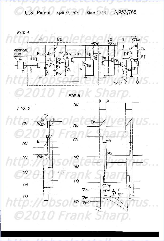 As a result, in the capacitor C1, voltage of sawtooth waveform as shown by the solid line in FIG. 5(b) is generated across said capacitor C1, which is subsequently applied to the base of a switching transistor Tr2. The latter transistor Tr2 starts conducting only when the voltage thus applied to the base thereof exceeds a D-C power source voltage E1 applied to the emitter of said transistor Tr2. Conduction of the switching transistor Tr2 results in a pulsating voltage of rectangular waveform, as shown by the solid line in FIG. 5(c), appearing at the common junction J1 of resistors R2 and R3, both of which are loaded on the collector of the transistor Tr2, due to the saturation characteristic of the transistor Tr2. The pulsating voltage at the common junction J1 is fed to the base of an amplifying transistor Tr3 so that the pulsating voltage is thereby amplified and phase-reversed and, as a result thereof, a phase-reversed pulsating voltage of the waveform as shown by the solid line in FIG. 5(d) appears at the common junction J2 of resistors R4 and R5, both of which are loaded on the collector of the transistor Tr3. This pulsating voltage at the common junction J2 is further phase-reversed by an amplifying transistor Tr4. Therefore, a voltage received by the transistor Tr6 from the collector of the amplifying transistor Tr4 has a waveform similar to that of the pulsating voltage applied to the base of the amplifying transistor Tr3.
 Simultaneously, the output pulse at the input terminal T1 is also applied to the base of a transistor Tr5. The transistor Tr5 acts to phase-reverse the output pulse to produce a pulsating voltage of a waveform as shown by the solid line in FIG. 5(e) at the collector of said transistor Tr5. The collector of this transistor Tr5 is connected with the collector of the transistor Tr4, which is in turn connected to the base of the transistor Tr6. This transistor Tr5 is non-conductive when voltage applied to the base threof is zero, in which condition the base of the transistor Tr6 receives a pulse of positive potential, i.e., a high level pulse, whereby it is held in a conductive state with the collector thereof in a zero volt or low level state. If the high level pulse is applied to the base of the transistor Tr4, this high level pulse is amplified and phasereversed by the transistor Tr4 to
produce a low level pulse from the collector thereof which is in turn fed to the transistor Tr6 to trigger the latter off. When the transistor Tr6 is thus triggered off, a high level voltage is produced from the collector of the transistor Tr6. In view of the foregoing, it can be seen that these transistors Tr4, Tr5 and Tr6 cooperate with each other to substantially act as a gating circuit while the pulsating voltage applied to the base of the transistor Tr6 from the transistor Tr4 acts as a trigger pulse. Accordingly, it is clear that the pulse appearing at the collector of the transistor Tr6 has a pulse width, as shown in FIG. 5(f), which corresponds to the pulse width W1 of the output pulse at the input terminal T1 extracted by the pulse width W2 of the high level pulse applied to the base of the transistor Tr4.
As stated hereinbefore, the start of the output pulse from the oscillator 4 can be accurately fixed while it is difficult to fix the termination of the pulse. Assuming, therefore, that the output pulse shown by the broken line in FIG. 5(a) and having a pulse width t1 to t4 which is larger than the desired pulse width t1 to t2 as shown by the solid line in FIG. 5(a), is applied to the pulse width control circuit 9 from the vertical oscillator 4, the transistor Tr1 becomes non-conductive and the voltage across the capacitor C1 accordingly increases as shown by the broken line in FIG. 5(b). On the other hand, the transistor Tr5 becomes non-conductive upon receiving of the input pulse at the base thereof at the time t1, causing the transistor Tr6 to start conducting.
When the voltage at the base of the transistor Tr2 exceeds the emitter voltage defined by the source E1, the transistors Tr2 and Tr3 become conductive and the junction point J2 becomes high level at the time t3 as shown in FIG. 5(d). Accordingly, the collector of the transistor Tr4 becomes low level causing the transistor Tr6 to become non-conductive whereby the collector of the transistor Tr6 becomes high level at the time t3.
From the foregoing, it is clear that, even if the width of the input pulse applied to the pulse width control circuit 9 is larger than the desired or predetermined width, the width output pulse of the control circuit 9 can be defined at the predetermined width as shown in FIG. 5(f).
Accordingly, a rectangular pulse having a predetermined pulse width is applied to the base of the input transistor Tr8 of the sawtooth signal generator 5, whereby the width of the flyback pulses included in the vertical deflection output can be maintained at the desired or predetermined width.
In the embodiment of FIG. 3, the pulse width of the output pulse of the pulse width control circuit 9 may not be suitable for the vertical output circuit. In this case, equalization of the pulse width can be achieved by varying the D-C voltage E1 supplied to the emitter of the transistor Tr2. Specifically, if the voltage E1 increases or decreases the pulse width at the output terminal F of the control circuit 9 is reduced or enlarged, respectively.
FIG. 6 shows another embodiment of the present invention in which the pulse width control circuit 9' receives a feedback signal from the deflection output circuit 8 so that the pulse width of the output signal from the width control circuit 9' can be advantageously controlled to maintain the width of the flyback pulse constant.
FIG. 7 shows the details of the width control circuit 9'. Referring now to FIG. 7, there is provided a differential amplifier 10 composed of transistors Tr13 and Tr14. The base of the transistor Tr13 receives the voltage on the capacitor C1 and feedback voltage fed back from the common junction J6 of the deflection output circuit through the integrator 11 and the resistors R5 and R6.
 The collector of the transistor Tr13 is connected to the base of the transistor Tr4 which constitutes the gating circuit in cooperation with the transistors Tr5 and Tr6. The switching level of the transistor Tr13 is defined by base voltage Eo appearing at the junction point J3 of the resistors R7 and R8.
 Operation of the circuit arrangement of FIGS. 6 and 7 will now be described.
It is assumed that, during operation of the control circuit 9' with the transistor Tr1 triggered off by the application of the low level pulse from the vertical oscillator 4, voltage supplied from the integrator 11 through the constant current resistor R5 and then a time constant adjusting resistor R6 charges the capacitor C1. Voltage of a sawtooth waveform as shown by the solid line in FIG. 8(b) is generated across the capacitor C1. This sawtooth voltage is subsequently fed to the differential amplifier 10. The charging speed of the capacitor C1 is defined by the voltage E F of the integrator 11.
When the voltage at the base of the transistor Tr13 exceeds the voltage Eo appearing at the base of the transistor Tr14, the transistor Tr13 becomes conductive with the output of the transistor Tr13 becoming low level. At the end of the input pulse, transistor Tr1 becomes conductive, the capacitor C1 is discharged, whereby the transistor Tr13 becomes non-conductive causing the output of the transistor Tr13 to become high level.
Therefore, pulses of rectangular waveform as shown by the solid line in FIG. 8(c) can be generated from the collector of the transistor Tr13. The pulses from the transistor Tr13 are amplified and phase-reversed by the transistor Tr4, which are in turn applied to the base of the transistor Tr7 through the transistor Tr5. It should be noted that the waveform of pulse at the junction J5 between the transistors Tr4 and Tr5 is shown by the solid lines in FIG. 8(d).
Simultaneously, the pulses from the input terminal T1 are also applied to the base of the transistor Tr6. Consequently, in a similar manner as in the circuit arrangement of FIG. 4, pulses of a waveform as shown by the solid line in FIG. 8(f) can be obtained at the collector of the transistor Tr7 and, hence, at the output terminal T2 of the width control circuit 9'.
The output pulses from the width control circ
uit 9' are supplied to the base of the transistor Tr9 through the transistor Tr8, said transistors Tr8 and Tr9 forming the sawtooth signal generator 5. Output from the sawtooth signal generator 5 is then applied to the base of the transistor Tr10 in the form of sawtooth pulses as shown, thereby causing the transistor Tr10 to generate trigger pulse for driving the vertical output transistors Tr11 and Tr12 in the known manner. The result is that vertical deflection output of a waveform as shown by the solid line in FIG. 8(g) appears at the junction J6 from which it is applied in part to the vertical deflection coil D and in part to the resistor R5 through the feedback loop. The deflection output that has been fed through the feedback loop is, prior to application thereof to the resistor R5, smoothed by the integrator 11 which is composed of the resistor R9 and the capacitor C2, to obtain a control voltage Ef of a suitably divided value. Assuming that the pulse width Pr of flyback pulses included in the vertical deflection output from the vertical output stage 8 varies, for example, gets smaller and is at a value Pr', the voltage Vr of the flyback pulse accordingly increases by the reason of the following equation: ##EQU1## wherein L is inductance of the vertical deflection coil D, i is vertical deflection current and K is a constant. In other words, while the peak level C of the flyback pulse is determined by the D-C power source voltage Vb2 and, therefore, does not vary, the average D-C voltage level Vm of the vertical deflection output is lowered to read a value Vm' as shown in FIG. 8(g).
Consequently, the pulse width control voltage Ef applied to the resistor R5 through the integrator 11 is lowered and the voltage to which the capacitor C1 is charged is also lowered. The result is such that, as indicated by the broken line in FIG. 8(b), the charging speed of the capacitor C1 is retarded whereby conduction of the transistor Tr13 is delayed. Accordingly, the waveforms of the pulses P1 and P2 at the junctions J4 and J5 are respectively narrowed as shown by the broken lines in FIG. 8(c) and (d). As a result thereof, the pulse width of the output pulse appearing at the output terminal T2 of the width control circuit 9' is broadened as shown by the broken line in FIG. 8(f) since the width of the pulse appearing at the terminal T2 is defined by a difference between the pulse at the base of the transistor Tr6 and the pulse at the base of the transistor Tr5. Therefore, the variation of the pulse width Pr of the vertical flyback pulse can be advantageously and effectively compensated for.
 FIG. 9 shows a further embodiment of the present invention. In the circuit arrangement of FIG. 9, the output from the oscillator 4 is first applied to the amplifying transistor Tr15 by which it is amplified and phase-reversed. From this transistor Tr15, the pulse of a waveform as shown in FIG. 10(a) is applied to the base of the transistor Pr1, thereby causing the latter to be triggered on. During a period in which the transistor Tr1 is non-conductive, the capacitor C1 is charged through the constant current transistor Tr16 and, when the transistor Tr1 starts conducting upon receipt of the pulse from the transistor Tr15, voltage charged in the capacitor C1 is discharged through the collector-emitter of the transistor Tr1. By this operation, voltage of the sawtooth waveform as shown in FIG. 10(b) is generated across the capacitor C1. This sawtooth voltage is subsequently applied to a differential amplifier 10 composed of a pair of transistors Tr13 and Tr14. The transistor Tr14 receives control voltage Ef fed from the junction point J6 of the vertical deflection output stage 8 through the integrator 11. By the level Ef of voltage fed to the base of the transistor Tr14, the slicing level of this sawtooth voltage can be varied and, hence, the pulse width of the pulse emerging from the collector of the transistor Tr14 can be varied as indicated by W1 in FIG. 10(c). The output pulse from the collector of the transistor Tr14 is fed to the base of the transistor Tr10 of the drive circuit 7 through the sawtooth signal generator 5. The vertical deflection output of a waveform as shown in FIG. 10(d) is generated at the junction J6 of the vertical output stage 8 after the output transistors Tr11 and Tr12 are driven by drive signal from the drive circuit 7.
 Assuming now that the pulse width W of the output from the oscillator 4 is suitably selected such as to be larger than that required in the vertical deflection output from the output stage 8, if the flyback pulse width Tr of the vertical deflection output becomes larger than the pulse width W, the voltage Vr of the flyback pulse is reduced for the same reason as in the embodiment of FIG. 7 while the peak level C thereof remains the same and, accordingly, the average D-C voltage Vm increases, resulting in increase of the control voltage Ef to be applied to the base of the transistor Tr14.
Therefore, the slicing level of the sawtooth voltage determined by the differential amplifier increases as indicated by the broken line in FIG. 10(b) and the pulse width of the output pulse emerging from the collector of the transistor Tr14 is reduced.
In this way, variation of the output pulse from the oscillator 4 resulting from the variation of the oscillator 4 itself
can be advantageously and adequately compensated for by the control circuit 9' and the average D-C voltage Vm of output from the output stage 8 and the flyback pulse of the vertical deflection output are respectively controlled to assume a predertermined value. FIG. 11 shows a still further embodiment of the present invention in which feedback voltage fed from the vertical output stage 8 is applied to the vertical oscillator 4 to maintain the width of the output pulse of the vertical oscillator 4 at a constant value.
The detailed circuit of the vertical oscillator 4 is shown in FIG. 12.
Referring to FIG. 12, the output pulse of the integrator 2 is applied to a base of a transistor Tr21 the collector of which is connected to the base of a transistor Tr22 through a resistor R21. The transistor Tr22 constitutes the differential amplifier in cooperation with a transistor Tr23 the base of which is connected to a capacitor C3 receiving voltage E1 of the D-C power source through a variable resistor VR.
The collector of the transistor Tr23 is connected to the base of an amplifying transistor Tr24 of which the collector is connected to the base of a transistor Tr25 through resistors R24 and R25. The collector of the transistor Tr25 is applied to the base of a transistor Tr26 and collector of a transistor Tr27 through a transistor Tr28. The junction point of the collector Tr27 and the base of the transistor Tr26 is grounded through a resistor R26 and a diode D1. The transistor Tr27 operates as a current stabilizer which is controlled by the collector output of the transistor Tr29. The transistor Tr27 receives control voltage Ec which is fed from the integrator 11 through a transistor Tr29. The collector output of the transistor Tr25 is applied to the base of the transistor Tr8 in the sawtooth signal generator 5.
Operation of the vertical deflection circuit shown in FIG. 12 will now be described.
Assuming that a main switch (not shown) for connection between the circuit and a power source (not shown) is turned on and a capacitor C3 of the oscillator 4, is not charged no voltage is applied to the base of the transistor Tr23 which forms the differential amplifier. During this condition, that is, when the base voltage Vb1 of the transistor Tr23 is zero, the transistor Tr23 is non-conductive while the collector voltage thereof is high and, therefore,
a transistor Tr24 is non-conductive. Likewisely, the transistors Tr21 and Tr25 have not yet been switched on and, accordingly, a transistor Tr28 is conductive. The switching transistor Tr26 for generation of sawtooth voltage is at this time non-conductive. During a period in which the transistor Tr21 is non-conductive, the base voltage Vb2 applied to the base of the transistor Tr22 is represented by the following equation: ##EQU2## wherein r21, r23 and r24 are resistances of the resistors R21, R22 and R23, respectively and E1 is the D-C power source voltage.
Subsequent switching on of the main switch permits the D-C power source voltage E1 to charge the capacitor C3 through the oscillation frequency adjusting resistor VR in such a manner as shown in FIG. 5(b). When the base voltage Vb1 of the transistor Tr23 starts to exceed the base voltage Vb2 of the transistor Tr22 at the time t1 a predetermined time after the capacitor C3 has been charged, the transistors Tr23 and Tr22 are respectively triggered on and off. Upon conduction of the transistor Tr23, the transistors Tr21 and Tr25 start conducting. Conduction of the transistor Tr25 results in reduction of the collector voltage thereof and, therefore, the transistor Tr28 is triggered off.
As the transistor Tr28 becomes non-conductive, the collector voltage of the transistor Tr28 increases, thereby triggering the transistor Tr26 on so that the charge on the capacitor C3 is discharged through the collector-emitter of the transistor Tr26. At this time, the collector current of the transistor Tr26 (i.e., the current flowing through the capacitor C3) is made to be constant by a constant current circuit which is composed of the transistor Tr27 and a diode D1. During this condition, the transistor Tr21 is conductive and, therefore, the base voltage Vb2 of the transistor Tr22 is lowered as represented by the following equation: ##EQU3##
Accodingly, discharge of the potential stored in the capacitor C3 continues at a constant current determined by the base potential of the transistor Tr27 until the base voltage Vb1 of the transistor Tr23 becomes equal to the base voltage ##EQU4## of the transistor Tr22 at the time t2. Thereafter, the transistor Tr23 is again triggered off while the transistor Tr22 is triggered on and this operation is repeated. The result is such that pulses of a rectangular waveform as shown in FIG. 13(e) are generated through the collector J9 of the transistor Tr25. The waveform of output pulse apearing at the output terminal T1 of the integrator 2 is as shown in FIG. 13(a) and this vertical synchronizing pulse is applied to the base of the transistor Tr21 whereby the oscillator 4 is oscillated in synchronizm with said vertical synchronizing pulses.
Waveforms of signals at the junctions J7, J8 and J6 are shown in FIGS. 13(c), (d) and (f), respectively.
On the other hand, though the start time t1 (FIG. 13(e )) of the output pulse from the oscillator 4 can be accurately determined because of synchronization with the vertical synchronizing pulse from the integrator 2, the termination t2 thereof cannot be accurately determined by the reason as hereinbefore described. If the pulse width of the output pulse from the oscillator 4 varies to represent a pulse width between t1 and t2' short of the required pulse width and the output pulse having such a reduced width is applied to the sawtooth signal generator 5 from the oscillator 4 the flyback pulse width Pr of the vertical deflection output at the junction J6 of the vertical output stage 8 is consequently reduced to a value Pr' as shown by the broken line in FIG. 13(f). The result is that the voltage Vr of the flyback pulse increases to represent a value Vr' by the reason as hereinbefore described in connection with the equation (1).
A voltage proportional to the average level Vm of D-C output voltage is extracted from a smoothing circuit 11, which is composed of the resistor R9
and a capacitor C4, and is subsequently fed to a transistor Tr29 for D-C amplification and phase-reversion. The transistor Tr29, upon receipt of this voltage from the smoothening circuit 11, generates voltage from the collector thereof which is used as a pulse width control voltage Ec which is subsequently applied to the base of the transistor Tr27. It is to be noted that the control voltage Ec increases in response to reduction of the flyback pulse width and, accordingly, the emitter-collector current of the transistor Tr27 is lowered upon receipt of the increased control voltage Ec' and the collector current of the transistor Tr26 is also lowered. As a result thereof, the speed at which the capacitor C3 charges is retarded as indicated by the broken line in FIG. 13(b), thus broadening the pulse width of the output pulse from the oscillator 4. In this way, the oscillation of the oscillator 4 is controlled to render the flyback pulse Pr' to become the required flyback pulse Pr.
It should be noted that, if the speed at which the capacitor C3 charges is varied by controlling the collector current of the switching transistor Tr26, the repetition frequency of the output pulse produced in the oscillator 4 may vary which is negligible in practice.

No comments:
Post a Comment
The most important thing to remember about the Comment Rules is this:
The determination of whether any comment is in compliance is at the sole discretion of this blog’s owner.
Comments on this blog may be blocked or deleted at any time.
Fair people are getting fair reply. Spam and useless crap and filthy comments / scrapers / observations goes all directly to My Private HELL without even appearing in public !!!
The fact that a comment is permitted in no way constitutes an endorsement of any view expressed, fact alleged, or link provided in that comment by the administrator of this site.
This means that there may be a delay between the submission and the eventual appearance of your comment.
Requiring blog comments to obey well-defined rules does not infringe on the free speech of commenters.
Resisting the tide of post-modernity may be difficult, but I will attempt it anyway.
Your choice.........Live or DIE.
That indeed is where your liberty lies.
Note: Only a member of this blog may post a comment.