


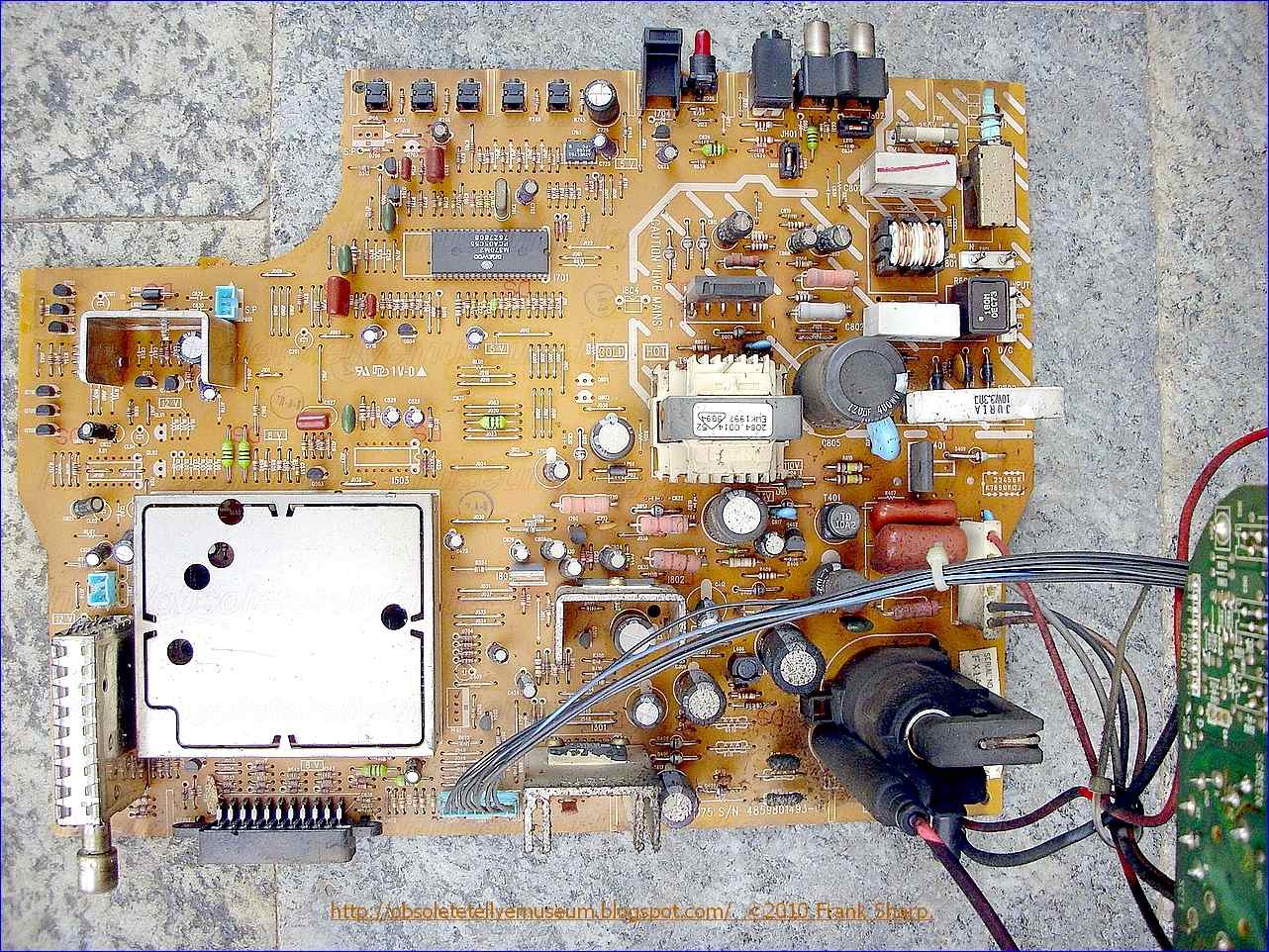


The PANASONIC TC-14B3RC CHASSIS Z-375 (DAEWOO CP-375) is a monocarrier carrying all functions of the receiver.
PHILIPS TDA8374 I2C-bus controlled economy PAL/NTSC and NTSC TV-processors:
GENERAL DESCRIPTIONcontrolled single-chip TV processors which are intended to
be applied in PAL/NTSC (TDA8374 and TDA8375) and
NTSC (TDA8373 and TDA8377) television receivers.
All ICs are available in an SDIP56 package and some
versions are also available in a QFP64 package. The ICs
are pin compatible so that with one application board
NTSC and PAL/NTSC (or multistandard together with the
SECAM decoder TDA8395) receivers can be built.
Functionally this IC series is split in to 2 categories:
• Versions intended to be used in economy TV receivers
with all basic functions
• Versions with additional functions such as E-W
geometry control, horizontal and vertical zoom function
and YUV interface which are intended for TV receivers
with 110° picture tubes.
FEATURES
Available in all ICs:• Vision IF amplifier with high sensitivity and good figures
for differential phase and gain
• PLL demodulator for the IF signal
• Alignment-free sound demodulator
• Flexible source selection with a CVBS input for the
internal signal and Y/C or CVBS input for the external
signal
• Audio switch
• The output signal of the CVBS (Y/C) switch is externally
available
• Integrated chrominance trap and band-pass filters
(auto-calibrated)
• Luminance delay line integrated
• A symmetrical peaking circuit in the luminance channel
• Black stretching of non-standard CVBS or luminance
signals
• RGB control circuit with black current stabilization and
white point adjustment
• Linear RGB inputs and fast blanking
• Horizontal synchronization with two control loops and
alignment-free horizontal oscillator
• Slow start and slow stop of the horizontal drive pulses
• Vertical count-down circuit
• Vertical driver optimized for DC-coupled vertical output
stages
• I2C-bus control of various functions
• Low dissipation
• Small amount of peripheral components compared with
competition ICs.
FUNCTIONAL DESCRIPTION
Vision IF amplifierThe IF amplifier contains 3 AC-coupled control stages with
a total gain control range which is higher than 66 dB.
The sensitivity of the circuit is comparable with that of
modern IF-ICs.
The video signal is demodulated by a PLL carrier
regenerator. This circuit contains a frequency detector and
a phase detector. During acquisition the frequency
detector will tune the VCO to the correct frequency.
The initial adjustment of the oscillator is realized via the
I2C-bus.
The switching, between SECAM L and L’, can also be
realized via the I2C-bus. After lock-in the phase detector
controls the VCO so that a stable phase relationship
between the VCO and the input signal is achieved.
The VCO operates at twice the IF frequency.
The reference signal for the demodulator is obtained by
using a frequency divider circuit.
The AFC output is obtained by using the VCO control
voltage of the PLL and can be read via the I2C-bus.
For fast search tuning systems the window of the AFC can
be increased by a factor of 3. The setting is realized with
the AFW bit.
Depending on the device type the AGC detector operates
on top-sync level (single standard versions) or on top-sync
and top-white level (multistandard versions).
The demodulation polarity is switched via the I2C-bus.
The AGC detector time constant capacitor is connected
externally. This is mainly because of the flexibility of the
application. The time constant of the AGC system during
positive modulation is rather long, this is to avoid visible
variations of the signal amplitude. To improve the speed of
the AGC system, a circuit has been included which detects
whether the AGC detector is activated every frame period.
When, during 3 frame periods, no action is detected the
speed of the system is increased. For signals without
peak-white information the system switches automatically
to a gated black level AGC. Because a black level clamp
pulse is required for this method of operation the circuit will
only switch to black level AGC in the internal mode.
The circuits contain a second fast video identification
circuit which is independent of the synchronization
identification circuit. Consequently, search tuning is also
possible when the display section of the receiver is used
as a monitor. However, this identification circuit cannot be
made as sensitive as the slower sync identification circuit
(SL) and it is recommended t
o use both identificationoutputs to obtain a reliable search system.
The identification output is applied to the tuning system via
the I2C-bus.
The input of the identification circuit is connected to pin 13,
the internal CVBS input (see Fig.1). This has the
advantage that the identification circuit can also be made
operative when a scrambled signal is received
[descrambler connected between the IF video output
(pin 6) and pin 13]. A second advantage is that the
identification circuit can be used when the IF amplifier is
not used (e.g. with built-i
n satellite tuners).The video identification circuit can also be used to identify
the selected CBVS or Y/C signal. The switching between
the two modes can be realized with bit VIM.
Video switches
The circuit has two CVBS inputs (CVBSint and CVBSext)
and a Y/C input. When the Y/C input is not required pin 11
can be used as the third CVBS input. The switch
configuration is illustrated in Fig.7. The selection of the
various sources is made via the I2C-bus.
The output signal of the CVBS switch is externally
available and can be used to drive the teletext decoder, the
SECAM add-on decoder and a comb filter.
In applications with comb filters a Y/C input is only possible
when additional switches are added. In applications
without comb filters the Y/C input signal can be switched
to the CVBS output.
Sound circuit
The sound band-pass and trap filters have to beconnected externally. The filtered intercarrier signal is fed
to a limiter circuit and is demodulated by a PLL
demodulator. This PLL circuit automatically tunes to the
incoming carrier signal, hence no adjustment is required.
The volume is controlled via the I2C-bus. The de-emphasis
capacitor has to be connected externally.
The non-controlled audio signal can be obtained from this
pin (pin 55) (via a buff
er stage).The FM demodulator can be muted via the I2C-bus. This
function can be used to switch-off the sound during a
channel change so that high output peaks are prevented
(also on the de-emphasis output).
The TDA8373 and TDA8374 contain an Automatic Volume
Levelling (AVL) circuit which automatically stabilizes the
audio output signal to a certain level which can be set by
the user via the volume control. This function prevents big
audio output fluctuations due to variations of the
modulation depth of the transmitter. The AVL function can
be activated via the I2C-bus.
Synchronization circuit
The sync separator is preceded by a controlled amplifier
which adjusts the sync pulse amplitude to a fixed level.
These pulses are fed to the slicing stage which operates at
50% of the amplitude.
The separated sync pulses are fed to the first phase
detector and to the coincidence detector. The coincidence
detector is used to detect whether the line oscillator is
synchronized and can also be used for transmitter
identification. The circuit can be made less sensitive by
using the STM bit. This mode can be used during search
tuning to ensure that the tuning system will not stop at very
weak input signals. The first PLL has a very high static
steepness so that the phase of the picture is independent
of the line frequency.
The line oscillator operates at twice the line frequency.
The oscillator capacitor is internal. Because of the spread
of internal components an auto
matic calibration circuit hasbeen added to the IC. The circuit compares the oscillator
frequency with that of the crystal oscillator in the colour
decoder.
This results in a free-running frequency which deviates
less than 2% from the typical value. When the IC isswitched on the horizontal output signal is suppressed and
the oscillator is calibrated as soon as all subaddress bytes
have been sent. When the frequency of the oscillator is
correct the horizontal drive signal is switched on. To obtain
a smooth switching on and switching off behaviour of the
horizontal output stage the horizontal output frequency is
doubled during switch-on and switch-off (slow start/stop).
During that time the duty cycle of the output pulse has such
a value that maximum safety is obtained for the output
stage.
To protect the horizontal output transistor, the horizontal
drive is immediately switched off (via the slow stop
procedure) when a power-on reset is detected. The drive
signal is switched on again when the normal switch-on
procedure is followed, i.e. all subaddress bytes must be
sent and, after calibration, the horizontal drive signal will
be released again via the slow start procedure.
When the coincidence detector indicates an out-of-lock
situation the calibration procedure is repeated.
The circuit has a secon
d control loop to generate the drivepulses for the horizontal driver stage. The horizontal
output is gated with the flyback pulse so that the horizontal
output transistor cannot be switched on during the flyback
time.
Adjustments can be made to the horizontal shift, vertical
shift, vertical slope, vertical amplitude and the S-correction
via the I2C-bus. In the TDA8375A, TDA8377A, TDA8375
and TDA8377 the E-W drive can also be adjusted via the
I2C-bus. The TDA8375 and TDA8377 have a flexible zoom
adjustment possibility for the vertical and horizontal
deflection. When the horizontal scan is reduced to display
4 : 3 pictures on a 16 : 9 picture tube an accurate video
blanking can be switched on to obtain well defined edges
on the screen. The geometry process
or has a differentialoutput for the vertical drive signal and a single-ended
output for the E-W drive (TDA8375A, TDA8377A,
TDA8375 and TDA8377). Overvoltage conditions (X-ray
protection) can be detected via the EHT tracking pin.
When an overvoltage condition is detected the horizontal
output drive signal will be switched off via the slow stop
procedure. However, it is also possible that the drive is not
switched off and that just a protection indication is given in
the I2C-bus output byte. The choice is made via the input
bit PRD
. The ICs have a second protection input on thephase-2 filter capacitor pin. When this input is activated the
drive signal is switched off immediately (without slow stop)
and switched on again via the slow start procedure.
For this reason this protection input can be used as ‘flash
protection’.
The drive pulses for the vertical sawtooth generator are
obtained from a vertical countdown circuit. This countdown
circuit has various windows depending on the incoming
signal (50 or 60 Hz and standard or non-standard).
The countdown circuit can be forced in various modes via
the I2C-bus. To obtain short switching times of the
countdown circuit during a channel change the divider can
be forced in the search window using the NCIN bit.
The vertical deflection can be set in the de-interlace mode
via the I2C-bus.
To avoid damage of the picture tube when the vertical
deflection fails, the guard output current of the TDA8350
and TDA8351 can be supplied to the beam current limiting
input. When a failure is detected the RGB outputs are
blanked and a bit is set (NDF) in the status byte of the
I2C-bus. When no vertical deflection output stage is
connected this guard circuit will also blank the output
signals. This can be overruled using the EVG bit.
Chrominance and luminance processing
The circuit contains a chrominance band-pass and trap
circuit. The filters are realized by using gyrator circuits.
They are automatically calibrated by comparing the tuning
frequency with the crystal frequency of the decoder.
The luminance delay line and the delay for the peaking
circuit are also realized by using gyrator circuits.
The centre frequency of the chrominance band-pass filter
is 10% higher than the subcarrier frequency. This
compensates for the high frequency attenuation of the IF
saw filter. During SECAM reception
the centre frequencyof the chrominance trap is reduced to obtain a better
suppression of the SECAM carrier frequencies. All ICs
have a black stretcher circuit which corrects the black level
for incoming video signals which have a deviation between
the black level and the blanking level (back porch).
The TDA8375A, TDA8377A, TDA8375 and TDA8377
have a defeatable coring function in the peaking circuit.
Some of the ICs have a YUV interface so that picture
improvement ICs such as the TDA9170 (contrast
improvement), TDA9177 (sharpness improvement) and
TDA4556 and TDA4566 (CTI) can be applied. When the
TDA4556 or TDA4566 is applied it is possible to increase
the gain of the luminance channel by using the GAI bit in
subaddress 03 so that the resulting RGB output signals
will not be affected.
Colour decoderNTSC signals (TDA8373 and TDA8377) or PAL/NTSC
signals (TDA8374 and TDA8375). The circuit contains an
alignment-free crystal oscillator, a killer circuit and two
colour difference demodulators. The 90° phase shift for the
reference signal is made internally.
The TDA8373 and TDA8377 contain an Automatic Colour
Limiting (ACL) circuit which prevents over saturation
occurring when signals with a high chroma-to-burst ratio
are received. This ACL function is also available in the
TDA8374 and TDA8375, however, it is only active during
the reception of NTSC signals.
The TDA8373 and TDA8377 have a switchable colour
difference matrix (via the I2C-bus) so that the colour
reproduction can be adapted to the market requirements.
In the TDA8374 and TDA8375 the colour difference matrix
switches automatically between PAL and NTSC, however,
it is also possible
to fix the matrix in the PAL standard.The TDA8374 and TDA8375 can operate in conjunction
with the SECAM decoder TDA8395 so that an automatic
multistandard decoder can be realized. The subcarrier
reference output for the SECAM decoder can also be used
as a reference signal for a comb filter. Consequently, the
reference signal is continuously available when PAL or
NTSC signals are detected and only present during the
vertical retrace period when a SECAM signal is detected.
Which standard the TDA8374 and TDA8375 can decode
depends on the external crystals. The crystal to be
connected to pin 34 must have a frequency of 3.5 MHz
(NTSC-M, PAL-M or PAL-N). Pin 35 can handle crystals
with a frequency of 4.4 and 3.5 MHz. Because the crystal
frequency is used to tune the line oscillator, the value of
the crystal frequency must be communicated to the IC via
the I2C-bus. It is also possible to use the IC in the so called
‘3-norma’ mode for South America. In that event one
crystal must be connected to pin 35 and the other two to
pin 34. Switching between the 2 latter crystals must be
performed externally. Consequently, the search loop of the
decoder must be controlled by the microcontroller.
To prevent calibration problems of the horizontal oscillator
the external switching between the two crystals should be
performed when the oscillator is forced to pin 35.
For a reliable calibration of the horizontal oscillator it is
very important that the crys
tal indication bits (XA and XB)are not corrupted. For this reason the crystal bits can be
read in the output bytes so that the software can check the
I2C-bus transmission.
RGB output circuit and black current stabilization
The colour difference signals are matrixed with the
luminance signal to obtain the RGB signals. Linear
amplifiers have been chosen for the RGB inputs so that the
circuit is suited for signals that are input from the SCART
connector. The insertion blanking can be switched on or off
using the IE1 bit. To ascertain whether the insertion pin
has a (continuous) HIGH level or not can be read via the
IN1 bit. The contrast and brightness control operate on
internal and external signals.
The output signal has an amplitude of approximately 2 V
(black-to-white) at nominal input signals and nominal
settings of the controls. To increase the flexibility of the IC
it is possible to add OSD and/or teletext signals directly at
the RGB outputs. This insertion
mode is controlled via theinsertion input. The action to switch the RGB outputs to
black has some delay which must be compensated for
externally.
The black current stabilization is realized by using a
feedback from the video output amplifiers to the RGB
control circuit. The black current of the 3 guns of the
picture tube is internally measured and stabilized.
The black level control is active during 4 lines at the end of
the vertical blanking. The vertical blanking is adapted to
the incoming CVBS signal (50 or 60 Hz). When the flyback
time of the vertical output stage is longer than the 60 Hz
blanking time, or when additional lines need to be blanked
(e.g. for close captioning lines) the blanking can be
increased to the same value as that of the 50 Hz blanking.
This can be set using the LBM bit. The leakage current is
measured during the first line and, during the following
3 lines, the 3 guns are adjusted to the required level.
The maximum acceptable leakage current is ±100 µA.
The nominal value of the black current is 10 µA. The ratio
of the currents for the various guns automatically tracks
with the white point adjustment so that the background
colour is the same as the adjusted white point.
The input impedance of the black current measuring pin is
14 kΩ. To prevent the voltage on this pin exceeding thesupply voltage during scan an internal protection diode
has been included.
When the TV receiver is switched on the black current
stabilization circuit is not active, the RGB outputs are
blanked and the beam current limiting input pin is
short-circuited. Only during the measuring lines will the
outputs supply a voltage of 4.2 V to the video output stage
to ascertain whether the picture tube is warming up. As
soon as the current supplied to the measuring input
exceeds a value of 190 µA the stabilization circuit will be
activated. After a waiting time of approximately 0.8 s the
blanking and beam current limiting input pins are released.
The remaining switch-on behaviour of the picture is
determined by the external time constant of the beam
current limiting network.
Adjustment of geometry control parameters
The deflection processor of the TDA8373 and TDA8374offers 5 control parameters for picture alignment:
• Vertical picture alignment
– S-correction
– vertical amplitude
– vertical slope
– vertical shift
– Horizontal shift alignment.
The TDA8375, TDA8377, TDA8375A and TDA8377A offer
in addition the following functions for horizontal alignment:
• E-W width
• E-W parabola/width
• E-W corner/parabola
• E-W trapezium correction.
It is important to notice that the ICs are designed for use
with a DC-coupled vertical deflection stage. This is the
reason why a vertical linearity alignment is not necessary
(and, therefore, not available).
For a particular combination of picture tube type and
vertical output stage and E-W output stage, it is
determined which are the required values for the settings
of S-correction. These parameters can be preset via the
I2C-bus and do not need any additional adjustment.
The remainder of the parameters are preset with the
mid-value of their control range (i.e. 1FH), or with the
values obtained by previous TV set adjustments.
The vertical shift control is intended for compensation of
off-sets in the external vertical output stage or in the
picture tube. It can be shown that without compensation
these off-sets will result in a certain linearity error,
especially with picture tubes that need large S-correction.
The total linearity error is in 1st order approximation
proportional to the value of the off-set and to the square of
the S-correction needed. The necessity to use the vertical
shift alignment depends on the expected off-sets in vertical
output stage and picture tube, on the required value of the
S-correction and on the demands upon vertical linearity.
For adjustment of the vertical shift and vertical slope
independent of each other, a special service blanking
mode can be entered by setting the SBL bit HIGH. In this
mode the RGB outputs are blanked during the second half
of the picture. There are
2 different methods for alignmentof the picture in vertical direction. Both methods make use
of the service blanking mode.
The first method is recommended for picture tubes that
have a marking for the middle of the screen. With the
vertical shift control the last line of the visible picture is
positioned exactly in the middle of the screen. After this
adjustment the vertical shift should not be changed.
The top of the picture is placed by adjusting the vertical
amplitude and the bottom by adjusting the vertical slope.
The second method is reco
mmended for picture tubes thathave no marking for the middle of the screen. For this
method a video signal is required in which the middle of the
picture is indicated (e.g. the white line in the circle test
pattern). With the vertical slope control the beginning of the
blanking is positioned exactly on the middle of the picture.
Then the top and bottom of the picture are placed
symmetrically with respect to the middle of the screen by
adjustment of the vertical amplitude and vertical shift. After
this adjustment the vertical shift has the correct setting and
should not be changed.
If the vertical shift alignment is not required VSH should be
set to its mid-value (i.e. VSH = 1FH). The top of the picture
is then placed by adjusting the vertical amplitude and the
bottom by adjusting the vertical slope. After the vertical
picture alignment the picture is positioned in the horizontal
direction by adjusting the horizontal shift.
To obtain the full range of the vertical zoom function with
the TDA8375 and TDA8377 the adjustment of the vertical
geometry should be carried out at a nominal setting of the
zoom DAC at position 19H.
PHILIPS TDA8356 DC-coupled vertical deflection circuit:
GENERAL DESCRIPTIONcolour deflection systems for field frequencies of
50 to 120 Hz. The circuit provides a DC driven vertical
deflection output circuit, operating as a highly efficient
class G system.
FEATURES
• Few external components• Highly efficient fully DC-coupled vertical output bridge
circuit
• Vertical flyback switch
• Guard circuit
• Protection against:
– Short-circuit of the output pins (7 and 4)
– Short-circuit of the output pins to VP.
• Temperature protection
• High EMC immunity because of common mode inputs
• A guard signal in zoom mode.
The vertical driver circuit is a bridge configuration. The
deflectioncoilisconnectedbetweentheoutputamplifiers,
which are driven in opposite phase. An external resistor
(RM) connected in series with the deflection coil provides
internal feedback information. The differential input circuit
is voltage driven. The input circuit has been adapted to
enable it to be used with the TDA9150, TDA9151B,
TDA9160A, TDA9162, TDA8366 and TDA8376 which
deliver symmetrical current signals. An external resistor
(RCON) connected between the differential input
determines the output current through the deflection coil.
Therelationshipbetweenthedifferentialinputcurrentand
the output current is defined by: Idiff× RCON= Icoil× RM.
The output current is adjustable from 0.5 A (p-p) to
2 A (p-p) by varying RM. The maximum
input differentialvoltage is 1.8 V. In the application it is recommended that
Vdiff= 1.5 V (typ). This is recommended because of the
spread of input current and the spread in the value of
RCON.
The flyback voltage is determined by an additional supply
voltage VFB. The principle of operating with two supply
voltages (class G) makes it possible to fix the supply
voltage VPoptimum for the scan voltage and the second
supply voltage VFBoptimum for the flyback voltage. Using
this method, very high efficiency is achieved.
The supply voltage VFB is almost totally available as
flyback voltage across the coil, this being possible due to
the absence of a decoupling capacitor (not necessary,
due to the bridge configuration). Built-in protections are:
• Thermal protection
• Short-circuit protection of the output pins (pins 4 and 7)
• Short-circuit protection of the output pins to VP.
A guard circuit VO(guard) is provided. The guard circuit is
activated at the following conditions:
• During flyback
• During short-circuit of the coil and during short-circuit of
the output pins (pins 4 and 7) to VP or ground
• During open loop
• When the thermal protection is activated.
This signal can be used for blanking the picture tube
screen.
Notes
1.
The linearity error is measured without S-correction and based on the same measurement principle as performed on
the screen. The measuring method is as follows: Divide the output signal I4− I7 (VRM) into 22 equal parts ranging
from 1 to 22 inclusive. Meas
ure the value of two succeeding parts called one block starting with part 2 and 3 (block 1)and ending with part 20 and 21 (block 10). Thus part 1 and 22 are unused. The equations for linearity error for
adjacent blocks (LEAB) and linearity error for not adjacent blocks (LENAB) are given below:
;
2.
Related to VP.
3.
The V values within formulae relate to voltages at or across relative pin numbers, i.e. V7-4/V1-2= voltage value across
pins 7 and 4 divided by voltage value across pins 1 and 2.
4.
V9-4 AC short-circuited.
5.
Frequency response V7-4/V9-4 is equal to frequency response V7-4/V1-2.
6.
At V(ripple)= 500 mV eff; measured across RM; fi= 50 Hz.
PHILIPS TDA6106Q Video output amplifier:
GENERAL DESCRIPTION
The TDA6106Q is a monolit
hic video output amplifier witha 6 MHz bandwidth and is contained in a 9-lead plastic
DIL-bent-SIL medium power package. The device uses
high-voltage DMOS technology and is intended to drive
the cathode of a CRT. To obtain maximum performance,
the amplifier should be used with black current control.
FEATURES
• No external heatsink required
• Black current measurement output for Automatic Black
current Stabilization (ABS)
• Internal 2.5 V reference circuit
• Internal protection against positive appearing CRT
flashover discharges
• Single supply voltage of 200 V
• Simple application with a variety of colour decoders
• Controlled switch-off behaviour.
Notes
1.
The cathode output is protected against peak currents (caused by positive voltage peaks during high-resistance
flash) of 5 A maximum with a charge content of 100 µC.
2.
The cathode output is also protected against peak currents (caused by positive voltage peaks during low-resistance
flash) of 10 A maximum with a charge content of 100 nC.
3.
Human body model: equivalent to discharging a 100 pF capacitor through a 1.5 kΩ resistor.
4.
Machine model: equivalent to discharging a 200 pF capacitor through a 0 Ω resistor.
Flashover protection
Th
e TDA6106Q incorporates a protection diode againstCRT flashover discharges that clamp the cathode output
voltage to a maximum of VDD+ Vdiode. To limit the diode
current, an external 1.5 kΩ carbon high-voltage resistor in
series with the cathode output and a 2 kV spark gap are
needed (for this resistor-value, the CRT has to be
connected to the main PCB). This addition produces an
increase in the rise and fall times of approximately 7.5 ns
and a decrease in the overshoot of approximately 1.3%.
VDD to GND must be decoupled:
1.
With a capacitor larger than 20 nF with good HF
behaviour (e.g. foil). This capacitor must be placed as
close as possibl
e to pins 6 and 4, but definitely within5 mm.
2.
With a capacitor larger than10 µF on the picture tube
base print (shared by three output stages).
Switch-off behaviour
The output pins of the TDA6106Q are still under the control
of the input pin for a supply voltage down to approximately
30 V.
PHILIPS TDA7056 3 W mono BTL audio output amplifier:
GENERAL DESCRIPTION
The TDA7056 is a mono output amplifier contained in a
9 pin medium power package.
The device is designed for battery-fed portable mono
recorders, radios and television.
FEATURES
• No external components
• No switch-on/off clicks
• Good overall stability
• Low power consumption
• Short circuit proof
• ESD protected on all pins.
FUNCTIONAL DESCRIPTION
The TDA7056 is a mono output amplifier, designed for
battery-fed
portable radios and mains-fed equipment suchas television. For space reasons there is a trend to
decrease the number of external components. For
portable applications there is also a trend to decrease the
number of battery cells, but still a reasonable output power
is required.
The TDA7056 fulfills both of these requirements. It needs
no peripheral components, because it makes use of the
Bridge-Tied-Load (BTL) principle. Consequently it has, at
the same supply voltage, a higher output power compared
to a conventional Single Ended output stage. It delivers an
output power of 1 W into a loudspeaker load of 8 Ω with 6
V supply or 3 W into 16 Ω loudspeaker at 11 V without
need of an external heatsink. The gain is internally fixed at
40 dB. Special attention is given to switch-on/off click
suppression, and it has a good overall stability. The load
can be short circuited at all input conditions.
Notes to the characteristics
1.
With a load connected to the outputs the quiescent current will increase, the maximum value of this increase being
equal to the DC output offset voltage divided by RL.
2.
The noise output voltage (RMS value) is measured with RS = 5 kΩ unweighted (20 Hz to 20 kHz).
3.
The noise output voltage (RMS value) at f = 500 kHz is measured with RS = 0 Ω and bandwidth = 5 kHz.
With a practical load (RL = 16 Ω, LL = 200 µH) the noise output current is only 50 nA.
4.
The ripple rejection is measured with RS = 0 Ω and f = 100 Hz to 10 kHz.
The ripple voltage (200 mV) is applied to the positive supply rail.
5.
RS = 5 kΩ
THOMSON TDA8138 5.1V +12V REGULATOR WITH DISABLE AND RESET:
DESCRIPTION
The TDA8138 is a monolithic dual positive voltage
regulator designed to provide fixed precision output
voltages of 5.1V and 12V at currents up to 1A.
An internal reset circuit generates a reset pulse
when the output 1 decrease below t
he regulatedvoltage value (for TDA8138 and TDA8138B).
Output 2 can be disabled by TTL input (for
TDA8138 and TDA8138A).
Short circuit and thermal protections are included
in all the versions.
.FIXED PRECISION OUTPUT 1 VOLTAGE
5.1V +/- 2%
.FIXED PRECISION OUTPUT 2 VOLTAGE
12V +/- 2%
.OUTPUT 1 WITH RESET FACILITY
.OUTPUT 2 WITH DISABLE BY TTL INPUT
.SHORT CIRCUIT PROTECTION AT BOTH
OUTPUTS
.THERMAL PROTECTION
.LOW DROP OUTPUT VOLTAGE
.AVAILABLE ALSO IN HEPTAWATT PACKAGE
IN TWO VERSIONS : TDA8138A (DISABLE
ONLY), TDA8138B (RESET ONLY)
The TDA8138 is a dual voltage regulator with Reset
and Disable (TD8138A : Disable only, TDA8138B :
Reset only).
The two regulation parts are supplied from one
voltage reference circuit trimmed by zener zap
during EWS test.
Since the supply voltage of this last is connected at
Pin 1 (VIN1), the regulator 2 will not work if Pin 1 is
not supplied.
The outputs stage have been realized in darlington
configuration with a drop typical 1.2V.
The disable circuit, switch-off the output 2 if a
voltage lower than 0.8V is applied at Pin 3
(Heptawatt) or Pin 4 (SIP9)
The Reset circuit checks the voltage at the out-
put 1. If this one goes below VOUT - 0.25V (4.85V
typ.), the comparator "a" (see Figure 1) discharges
rapidly the capacitor Ce and the reset output goes
at once Low. When the voltage at the out1 rises
above VOUT - 0.2V (4.9V typ.), the voltage VCe
increases linearly to 2.5V corresponding to a delay
td following the law : t1 = Ce ⋅ 2.5V
10µA
(see Figure 2),
then the reset output goes high again. To avoid
gliches in the reset output, the second comparator
"b" has a large hysteresis (1.9V).
PHILIPS TDA8395 SECAM decoder:
The TDA8395 is a self-calibrating, fully integrated SECAM decoder. The IC should preferably be used in conjunction with
the PAL/NTSC decoder TDA8362 or TDA8366 and with the switched capacitor baseband delay circuit TDA4660. The IC
incorporates HF and LF filters, a demodulator and an identification circuit (luminance is not processed in this IC). The IC
needs no adjustments and very few external components are required. A highly stable reference frequency is required
for calibration and a two-level sandcastle pulse for blanking and burst gating.
FEATURES
• Fully integrated filters
• Alignment free
• For use with baseband delay.
FUNCTIONAL DESCRIPTION
The TDA8395 is a self-ca
librating SECAM decoderdesigned for use with a baseband delay circuit.
During frame retrace a 4.433619 MHz reference frequency
is used to calibrate the filters and the demodulator. The
reference frequency should be very stable during this
period.
The Cloche filter is a gyrator-capacitor type filter the
resonance frequency of which is controlled during the
calibration period and offset during scan; this ensures the
correct frequency during calibration.
The demodulator is a Phase-Locked Loop (PLL) type
demodulator which uses the frequency reference and the
bandgap reference to force the PLL to the required
demodulation characteristic.
The low frequency de-emphasis is matched to the PLL and
is controlled by the tuning voltage of the PLL.
A digital identification circuit scans the incoming signal for
SECAM (only line-identification is implemented). The
identification circuit needs to communicate with the
TDA8362 to guarantee that the output signal from the
decoder is only available when no PAL signal has been
identified. If a SECAM signal is decoded a request for
colour-on is transmitted to pin 1 (current is sunk). If the
signal request is granted (i.e. pin 1 is HIGH therefore no
PAL) the colour difference outputs (−(B−Y) and −(R−Y))
from the TDA8362 are high impedance and the output
signals from the TDA8395 are switched ON.
If no SECAM signal is decoded during a two-frame period
the demodulator will be initialized before another attempt
is made also during a two-frame period. The CD outputs
will be blanked or high-impedance depending on the logic
level at pin 1.
A two-level sandcastle pulse generates the required
blanking periods and, also, clocks the digital identification
pulse on the falling edge of the burst gate pulse. To enable
the calibration period to be defined the vertical retrace is
discriminated from the horizontal retrace, this is achieved
by m
easuring the width of the blanking period.APPLICATION INFORMATION
The leakage current at pin 8 should be well below 20 nA to meet the specification of the black levels (C8 = 220 nF).
The leakage current at pin 7 should be well below 60 nA to meet the specification of the Cloche resonance frequency
(C7 = 100 nF).
The capacitors C7 and C8 should be connected to the ground pin as close as possible to the package. If not, this can
result in a black level error for both channels.
TEST INFORMATION
The performance of the Cloche filter can be measured at pin 2. The use of a FET-probe is advised for low capacitive
loading.
STV8225 AM SIF CIRCUIT:
DESCRIPTION
The STV8225is intended for the demodulationof
the AM soundof the Lstandard.
Used as an add on to the STV8224 it permits to
design a multistandard set with the needed
switchesfor one SCART plug.
.AM/FM AUDIO SWITCH
.AV/TVAUDIO SWITCH
.MUTE INPUT
PHILIPS TDA4665 Baseband delay line:
GENERAL DESCRIPTION
The TDA4665 is an integrated baseband delay line circuit
with one line delay. It is suitable for decoders with
colour-difference signal outputs ±(R−Y) and ±(B−Y).
FEATURES
• Two comb filters, using the switched-capacitor
technique, for one line delay time (64 µs)
• Adjustment-free application
• No crosstalk between SECAM colour carriers (diaphoty)
• Handles negative or positive colour-difference input
signals
• Clamping of AC-coupled input signals (±(R−Y) and
±(B−Y))
• VCO without external components
• 3 MHz internal clock signal derived from a 6 MHz CCO,
line-locked by the sandcastle pulse (64 µs line)
• Sample-and-hold circuits and low-pass filters to
suppress the 3 MHz clock signal
• Addition of delayed and non-delayed output signals
• Output buffer amplifiers
• Comb filtering functions for NTSC colour-difference
signals to suppress cross-colour.
The STR-S5707 and STR-S5708 are specifically designed to meet
the requirement for increased integration and reliability in off-line quasi-
resonant flyback converters with indirect feedb
ack. Each deviceincorporates the primary control and proportional drive circuit with a
third-generation high-voltage bipolar switching transistor.
Crucial system parameters such as maximum ON time and OFF
time are fixed during manufacture. Local control circuit decoupling and
layout are optimized within each device.
Cycle-by-cycle current limiting, under-voltage lock-out with hyster-
esis, over-voltage protection, and thermal shutdown protect these
devices during all normal and overload conditions. Over-voltage
protection and thermal shutdown are latched after a short delay. A
primary-side error amplifier with reference is included to facilitate
regulation from an auxiliary or bias winding of the power transformer. A
versatile triple-level inhibit circuit includes the OFF time synchronization
required to establish qu
asi-resonant operation. The inhibit function hasalso been expanded to initiate operation in stand-by mode in which the
power supply delivers a small fraction of the steady-state output power.
The dual requirements of
impedance and steady-state thermal resistance are satisfied in an over-
molded single-in-line power package.
Proven in substantial volumes, this device and its fixed-frequency
counterparts represents a significant advance in off-line SMPS reliability
growth and integration.
FEATURES
I Quasi-Resonant Operation for Low EMI and High Efficiency
I Low-Power Output Standby Mode
I Indirect Feedback from Auxiliary Winding
Reduces External Component Count
I Pulse-by-Pulse Over-Current Protection
I Latched Over-Voltage and Thermal Protection
I Third-Generation Switching Transistor with Proportional Drive
I Maximum ON Time and Off Time Set During Manufacture
I Internal Under-Voltage Lockout with Hysteresis
I Over-Molded SIP with Integral Isolated Heat Spreader
Other References:
Siemens “Control IC for Single-Ended and Push-Pull Switched-Mode Power Supplies (SMPS)”, , Semiconductor Group, TDA 4718 A.
“Feed Forward Converter SMPS with Several Output Voltages (5V/10A, ± 12V/2A)”, SIEMENS Application Note, TDA 4718 and SIPMOS®FET.
Mammano, Robert A., “Applying the UCC3570 Voltage-Mode PWM Controller to Both Off-Line and DC/DC Converter Designs”, Unitrode Corporation, Application Note U-150, Advanced Technology 1994.
Balakrishnan, Balu, “Three Terminal Off-Line Switching Regulator Reduces Cost and Parts Count”, Official Proceedings of the Twenty-Ninth International Power Conversion Conference, at 267 (1994).
Balakrishnan, Balu, “Next Generation, Monolithic Off-Line Switcher Improves Performance, Flexibility”, Power Integrations, Inc., PCIM Apr. 2000.
Davis, Sam, “Why Don't More Universities Teach Power Electronics Design?” PCIM Apr. 2000.
Linear Technology LT1070/LT1071 Data Sheet, (1989).
Linear Technology, LT1072 Data Sheet, (1988).
Linear Technology, LT1074/LT1076 Data Sheet, (1994).
Lenk, John D., “Simplified Design of Switching Power Supplies,” Butterworth-Heinemann (1995).
Pressman, Abraham I., “Switching Power Supply Design,” McGraw-Hill, Inc. (1998).
Xunwei Zhou et al.; Improve Light Load Efficiency for Synchronous Rectifier Buck Converter, IEEE, at 295 (1999).
Balu Balakrishnan, Low-power switchers expand reach, Electronic Engineering Times, Aug. 29, 1994, at 52.
Design of Isolated Converters Using Simple Switchers, Application Note 1095, National Semiconductor (Aug. 1998) (“LM285X Data Sheet”).
CS5124/6 Data Sheet, Cherry Semiconductor (1999) (CS5124 Data Sheet).
Irving M. Gottlieb, Power Supplies, Switching Regulators, Inverters, and Converters .
Panov and Jovanovic, Adaptive Off-Time Control For Variable-Frequency, Soft-Switched Flyback Converter At Light Loads, 1999 IEEE.
Xunwei Zhou, Mauro Donati, Luca Amoroso, Fred C. Lee, Improved Light-Load Efficiency for Synchronous Rectifier Voltage Regulator Module, IEEE Transactions on Power Electronics, vol. 15., No. 5., Sep. 2000.
Wayne M. Austin, Variable-pulse modulator improves power-supply regulation, Jun. 25, 1987.
F. J. De Stasi, T. Szepesi, A 5A 100 KHZ Monolitihc Bipolar DC/DC Converter, The European Power Electronics Association (1993).
Unitrode Current Mode PWM Spec sheet for US1846/7, UC2846/7, UC3836/7.
Motorola, Inc., A 100 kHz FET Switcher, TDT-101 TMOS Power Fet Design Tips sheet.
M. Goodman and O. Kuhlmann, Current mode control of switching regulators, IEEE, Oct. 1984.
Micro Linear preliminary spec sheet, ML4803, 8-Pin PFC and PWM Controller Combo, Feb. 1999.
Fairchild Advance Specification for FAN7554/D product, Rev. 0.1, 2000.
Robert Boschert, Flyback converters: Solid-state solution to low-cost switching power supplies, Electronics, Dec. 21, 1978.
Ravindra Ambatipudi, Improving Transient Response of Opto-Isolated Converters, PC/M May 1997.
Linear Technology's LT1070/LT1071 Design Manual, Application Note 19, Jun. 1986.
Linear Technology's LT1241 Data Sheet.
Jim Williams, Regulator IC speeds design of switching power supplies .
Carl Nelson, Switching controller chip handles 100W from a 5-pin package, Electronic Design, Dec. 26, 1985.
Siemens TDA 4714 C, TDA 4716 C, Sep. 1994.
Siemens TDA 4718 A, Dec. 1995.
Texas Instruments TL5001, TL5001A.
Unitrode Corporation UCC1809-1/-2/ UCC2809-1/-2/UCC3809-1/12 Data Sheet—Nov. 1999.
L. Calderoni, L. Pinol, V. Varoli, Optimal Feed-Forward Compensation for PWM DC/DC Converters, IEEE, 1990.
L. Calderoni, L. Pinol, V. Varoli, Optimal Feed-Forward Compensation for PWM DC/DC Converters with “Linear” and “Quadratic” Conversion Ratio, IEEE, 1992.
Maige, Philippe, “A Universal Power Supply Integrated Circuit for TV and Monitor Applications”.
LM2825 Application Information Guide.
Design of Isolated Converters Using Simple Switchers.
Motorola—Low cost 1.0 A Current Source for Battery Chargers.
Infineon Technologies Application Note: AN-SMPS-1683X-1.
Cherry Semiconductor High Performance, Integrated Current Mode PWM Controllers.
Cherry Semiconductor High Performance, Integrated Current Mode PWM Controllers CS5124/6.
Abstract data sheet for FA3641P.
Fairchild Semiconductor FAN7554/D Versatile PWM Controller.
Ambatipudi, Ravindra, Improving Transient Response of Opto-Isolated Converters.
National Semiconductor LM2825 Integrated Power Supply 1A DC-DC Converter.
Williams, Jim, “Regulator IC speeds design of switching power supplies.”
Nelson, Carl “Switching controller chip handles 100 W from a-5-pin package.”
Unitrode Corporation UCC1570/UCC2570/UCC3570 Data Sheet—Apr. 1999, Revised Jul. 2000.
STMicroelectronics, VIPer100/SP, VIPer100A/ASP data sheet (May 1999).
FA3641P(N), FA3647P(N) Spec Sheet.
Keith Billings, Switchmode Power Supply Handbook, McGraw-Hill, Inc. (1989).
Xunwei Zhou et al.; “Improve Light Load Efficiency for Synchronous Rectifier Buck Converter,” 1999 IEEE at 295.
Balakrishnan, Balu “Next Generation, Monolithic Off-Line Switcher Improves Performance, Flexibility,” Power Integrations, Inc., PCIM Apr. 2000.
Linear Technology LT 1070 Design Manual.
Siemens IC for Switched-Mode Power Supplies spec.
De Stasi, et al. “A 5A 100 Khz monolithic bipolar DC/DC converter”.
Linear Technology 5A and 2.5A High Efficiency Switching Regulators.
Boschert, Robert. “Flyback converters: solid-state solution to low-cost switching power supplies,” , Electronics, Dec. 21, 1978.
Linear Technology data sheet—5A and 2.5A High Efficiency Switching Regulators.
R. Mammano, Application Note U-150 Applying the UCC3570 Voltage-Mode PWM Controller to Both Off-Line and DC/DC Converter Designs.
Unitrode Corporation UCC1570/UCC2570/UCC3570—Low Power Pulse Width Modulator—data sheet (Apr. 1999, Revised Jul. 2000).
Power Integrations, Inc.'S Disclosure of Asserted Claims and Preliminary Infringement Contentions, Power Integrations, Inc. v. System General Corporation & System General USA, United States District Court, Northern District of California, San Francisco Division, Case No. C04 2581 JSW, Apr. 15, 2005.
Power Integrations, Inc.'S Revised Disclosure of Asserted Claims and Preliminary Infringement Contentions, Power Integrations, Inc. v. System General Corporation & System General USA, United States District Court, Northern District of California, San Francisco Division, Case No. C04 2581 JSW, May 24, 2005.
Defendants System General Corporation and System General USA's Preliminary Invalidity Contentions, Power Integrations, Inc. v. System General Corporation& System General USA, United States District Court, Northern District of California, San Francisco Division, Case No. C04 2581 JSW, May 27, 2005.
Fourth Joint Status Report, Power Integrations, Inc. v. System General Corporation& System General USA, United States District Court, Northern District of California, San Francisco Division, Case No. C04 2581 JSW, Jul. 5, 2006.
Final Initial and Recommended Determinations, In the Matter of Certain Power Supply Controllers and Products Containing the Same, United States International Trade Commission, Washington, DC 20436, Before the Honorable Paul J. Luckern, Administrative Law Judge, Inv. No. 337-TA-541, May 15, 2006.
Respondent System General Corporation's Petition for Review of the Final Intial Determination, In the Matter of Certain Power Supply Controllers and Products Containing the Same, United States International Trade Commission, Washington, DC 20436, Before the Honorable Paul J. Luckern, Administrative Law Judge, Inv. No. 337-TA-541, May 26, 2006.
Complainant Power Integration, Inc.'s Opposition to Respondent System General Corp.'s Petition for Review of the Final Intial Determination, In the Matter of Certain Power Supply Controllers and Products Containing the Same, United States International Trade Commission, Washington, DC 20436, Before the Honorable Paul J. Luckern, Administrative Law Judge, Inv. No. 337-TA-541, Jun. 5, 2006.
Response of the Office of Unfair Import Investigations to Respondent System General Corp.'s Petition for Review of the Final Intial Determination, In the Matter of Certain Power Supply Controllers and Products Containing the Same, United States International Trade Commission, Washington, DC 20436, Before the Honorable Paul J. Luckern, Administrative Law Judge, Inv. No. 337-TA-541, Jun. 5, 2006.
Notice of Commission Determination Not to Review a Final Initial Determination of Violation of Section 337; Schedule for Filing Written Submissions on Remedy, The Public Interest, and Bonding, In the Matter of Certain Power Supply Controllers and Products Containing the Same, United States International Trade Commission, Washington, DC 20436, Before the Honorable Paul J. Luckern, Administrative Law Judge, Inv. No. 337-TA-541, Jun. 30, 2006.
International Trade Commission, In The Matter Of Certain Power Supply Controllers And Products Containing The Same; Notice Of Commission Determination Not To Review a Final Initial Determination of Violation of Section 337; Schedule for Filing Written Submissions on Remedy, the Public Interest, and Bonding, Federal Register, vol. 71, No. 131 at 38901-02, Jul. 10, 2006.
Brief for Appellant System General Corp., System General Corp. v. International Trade Commission and Power Integrations, Inc., United States Court of Appeals for the Federal Circuit, On appeal from the United States International Trade Commission in Investigation No. 337-TA-541, Apr. 23, 2007.
Complainant Power Integrations, Inc.'s Posthearing Statement (Fully-Redacted), In the Matter of Certain Power Supply Controllers and Products Containing Same, United States International Trade Commission, Washington, DC 20436, Before the Honorable Paul J. Luckern, Administrative Law Judge, Inv. No. 337-TA-541, Feb. 10, 2006.
Respondent System General Corporation's Post-Hearing Brief (Fully-Redacted), In the Matter of Certain Power Supply Controllers and Products Containing Same, United States International Trade Commission, Washington, DC 20436, Before the Honorable Paul J. Luckern, Administrative Law Judge, Inv. No. 337-TA-541, Feb. 10, 2006.
Post-Hearing Brief of the Commission Investigative Staff (Fully-Redacted), In the Matter of Certain Power Supply Controllers and Products Containing Same, United States International Trade Commission, Washington, DC 20436, Before the Honorable Paul J. Luckern, Administrative Law Judge, Inv. No. 337-TA-541, Feb. 14, 2006.
Complainant Power Integrations, Inc.'s Posthearing Reply Statement (Fully-Redacted), In the Matter of Certain Power Supply Controllers and Products Containing Same, United States International Trade Commission, Washington, DC 20436, Before the Honorable Paul J. Luckern, Administrative Law Judge, Inv. No. 337-TA-541, Feb. 24, 2006.
Respondent System General Corporation's Post-Hearing Reply Brief (Fully-Redacted), In the Matter of Certain Power Supply Controllers and Products Containing Same, United States International Trade Commission, Washington, DC 20436, Before the Honorable Paul J. Luckern, Administrative Law Judge, Inv. No. 337-TA-541, Feb. 24, 2006.
United States Court of Appeals for the Federal Circuit 2007-1082, Judgement, System General Corp. v. International Trade Commission and Power Integrations, Inc., On Appeal from the United States International Trade Commission, In Case No. 337-TA-541, Before the Honorable Pauline Newman, Circuit Judge, the Honorable Raymond C. Clevenger, III, Senior Circuit Judge, and Timothy B. Dyk, Circuit Judge, Nov. 19, 2007.
“Advanced Voltage Mode Pulse Width Modulator,” UNITRODE Corp., UCC15701/2, UCC25701/2, UCC35701/2, Jan. 2000, pp. 1-10.
“Advance Information: High Voltage Switching Regulator,” MC33362, MOTOROLA Inc., Motorola Analog IC Device Data, Rev 2, 1996, pp. 1-12.
I have a 20 year old Panasonic TV exactly like this one, right down to the model number, and use it for playing old games, however due to ageing the overscan is a tiny bit off and the picture occasionally moves/bleeds slightly when a sudden change in light happens, which is reduced significantly if I turn the contrast right down (but that decreases the vibrancy).
ReplyDeleteI can't find anything about it in the guide, but I've read that all Panasonic TVs made from 1996 onwards have a hidden service menu in which overscan, stability and voltage values can be modified to refine the picture of displays that are showing signs of ageing, like my one. A lot of sources claim that for most European Panasonic TVs of this era, the menu is accessed by holding down the volume/channel down button on the TV while pressing the R button on the remote three times, but doing so brings up nothing unfortunately. Do you know the service menu code for this model?
The service mode you intend to access can be activated only with a special remote control unit version which contains all specific service keyboard functions obtainable in the MCU firmware during setup of the basic setups in the factory.
ReplyDeleteThis remote control was not available to the public but only to authorized service center by Panasonic.
Your tv set is more likely defective in one or more parts such as Frame (Vertical) deflection and in EHT part or supply.
Trying to "adjust" picture dimensions to overcome or override / cheat a defective apparatus is not the right way to do things, as it may indicate a further worsening of defective sections which may end in brief future to an broken * unusable set.
*translated the short way means happy gaming ------> GAME OVER !