


 What is a Flyback Transformer?
The low cost, simplicity of design and intrinsic efficiency of flyback transformers have made them a popular solution for power supply designs of below 100W to 150W. Other advantages of the flyback transformer over circuits with similar topology include isolation between primary and secondary and the ability to provide multiple outputs and a choice of positive or negative voltage for the output.
Flyback transformer, or, line output transformers are a part of the power supplies in cathode ray tubes. The flyback transformer generates a high voltage, as needed by the CRT display or similar devices (e.g. plasma lamps). A flyback transformer generates a voltage between a few kilovolts to 50 kilovolts and uses high frequency switched currents between 17 kHz and 50 kHz.
The chief difference between a flyback transformer and main/audio transformer is that flybacks transfer as well as store energy, for a just a fraction of an entire switching period. The secret behind that is the coil winding on a ferrite core that has an air gap; it increases the magnetic circuit reluctance for storing the energy.
The reason it is called a flyback transformer is because the primary winding uses a relatively low-voltage saw-tooth wave. The wave gets strengthened first and then gets switched off abruptly; this causes the beam to fly back from right to left on the display.
Applications
Cathode ray tube.
Televisions.
Plasma Lamps.
Any display requiring high voltage to operate and much more.
Power supply Description based on TDA4601d (SIEMENS)
 TDA4601 Operation. * The TDA4601 device is a single in line, 9 pin chip. Its predecessor was the TDA4600 device, the TDA4601 however has improved switching, better protection and cooler running. The (SIEMENS) TDA4601 power supply is a fairly standard parallel chopper switch mode type, which operates on the same basic principle as a line output stage. It is turned on and off by a square wave drive pulse, when switched on energy is stored in the chopper transformer primary winding in the form of a magnetic flux; when the chopper is turned off the magnetic flux collapses, causing a large back emf to be produced. At the secondary side of the chopper transformer this is rectified and smoothed for H.T. supply purposes. The advantage of this type of supply is that the high chopping frequency (20 to 70 KHz according to load) allows the use of relatively small H.T. smoothing capacitors making smoothing easier. Also should the chopper device go short circuit there is no H.T. output. In order to start up the TDA4601 I.C. an initial supply of 9v is required at pin 9, this voltage is sourced via R818 and D805 from the AC side of the bridge rectifier D801, also pin 5 requires a +Ve bias for the internal logic block. (On some sets pin 5 is used for standby switching). Once the power supply is up and running, the voltage on pin 9 is increased to 16v and maintained at this level by D807 and C820 acting as a half wave rectifier and smoothing circuit. PIN DESCRIPTIONS Pin 1 This is a 4v reference produced within the I.C. Pin 2 This pin detects the exact point at which energy stored in the chopper transformer collapses to zero via R824 and R825, and allows Q1 to deliver drive volts to the chopper transistor. It also opens the switch at pin 4 allowing the external capacitor C813 to charge from its external feed resistor R810. Pin 3 H.T. control/feedback via photo coupler D830. The voltage at this pin controls the on time of the chopper transistor and hence the output voltage. Normally it runs at Approximately 2v and regulates H.T. by sensing a proportion of the +4v reference at pin 1, offset by conduction of the photo coupler D830 which acts like a variable resistor. An increase in the conduction of transistor D830 and therefor a reduction of its resistance will cause a corresponding reduction of the positive voltage at Pin 3. A decrease in this voltage will result in a shorter on time for the chopper transistor and therefor a lowering of the output voltage and vice versa, oscillation frequency also varies according to load, the higher the load the lower the frequency etc. should the voltage at pin 3 exceed 2.3v an internal flip flop is triggered causing the chopper drive mark space ratio to extend to 244 (off time) to 1 (on time), the chip is now in over volts trip condition. Pin 4 At this pin a sawtooth waveform is generated which simulates chopper current, it is produced by a time constant network R810 and C813. C813 charges when the chopper is on and is discharged when the chopper is off, by an internal switch strapping pin 4 to the internal +2v reference, see Fig 2. The amplitude of the ramp is proportional to chopper drive. In an overload condition it reaches 4v amplitude at which point chopper drive is reduced to a mark-space ratio of 13 to 1, the chip is then in over current trip. The I.C. can easily withstand a short circuit on the H.T. rail and in such a case the power supply simply squegs quietly. Pin 4 is protected by internal protection components which limit the maximum voltage at this pin to 6.5v. Should a fault occur in either of the time constant components, then the chopper transistor will probably be destroyed. Pin 5 This pin can be used for remote control on/off switching of the power supply, it is normally held at about +7v and will cause the chip to enter standby mode if it falls below 2v. Pin 6 Ground. Pin 7 Chopper switch off pin. This pin clamps the chopper drive voltage to 1.6v in order to switch off the chopper. Pin 8 Chopper base current output drive pin. Pin 9 L.T. pin, approximately 9v under start-up conditions and 16v during normal running, Current consumption of the I.C. is typically 135mA. The voltage at this pin must reach 6.7v in order for the chip to start-up.Semiconductor
circuit for supplying power to electrical equipment, comprising a
transformer having a primary winding connected, via a parallel
connection of a collector-emitter path of a transistor with a first
capacitor, to both outputs of a rectifier circuit supplied, in turn, by a
line a-c voltage; said transistor having a base controlled via a
second capacitor by an output of a control circuit acted upon, in turn
by the rectified a-c line voltage as actual value and by a reference
voltage; said transformer having a first secondary winding to which the
electrical equipment to be supplied is connected; said transformer
having a second secondary winding with one terminal thereof connected to
the emitter of said transistor and the other terminal thereof
connected to an anode of a first diode leading to said control circuit;
said transformer having a third secondary winding with one terminal
thereof connected, on the one hand, via a series connection of a third
capacitor with a first resistance, to the other terminal of said third
secondary winding and connected, on the other hand, to the emitter of
said transistor, the collector of which is connected to said primary
winding; a point between said third capacitor and said first resistance
being connected to the cathode of a second diode; said control circuit
having nine terminals including a first terminal delivering a
reference voltage and connected, via a voltage divider formed of a
third and fourth series-connected resistances, to the anode of said
second diode; a second terminal of said control circuit serving for
zero-crossing identification being connected via a fifth resistance to
said cathode of said second diode; a third terminal of said
control-circuit serving as actual value input being directly connected
to a divider point of said voltage divider forming said connection of
said first terminal of said control circuit to said anode of said
second diode; a fourth terminal of said control circuit delivering a
sawtooth voltage being connected via a sixth resistance to a terminal
of said primary winding of said transformer facing away from said
transistor; a fifth terminal of said control circuit serving as a
protective input being connected, via a seventh resistance to the
cathode of said first diode and, through the intermediary of said
seventh resistance and an eighth resistance, to the cathode of a third
diode having an anode connected to an input of said rectifier circuit; a
sixth terminal of said control circuit carrying said reference
potential and being connected via a fourth capacitor to said fourth
terminal of said control circuit and via a fifth capacitor to the anode
of said second diode; a seventh terminal of said control circuit
establishing a potential for pulses controlling said transistor being
connected directly and an eighth terminal of said control circuit
effecting pulse control of the base of said transistor being connected
through the intermediary of a ninth resistance to said first capacitor
leading to the base of said transistor; and a ninth terminal of said
control circuit serving as a power supply input of said control circuit
being connected both to the cathode of said first diode as well as via
the intermediary of a sixth capacitor to a terminal of said second
secondary winding as well as to a terminal of said third secondary
winding.
TDA4601 Operation. * The TDA4601 device is a single in line, 9 pin chip. Its predecessor was the TDA4600 device, the TDA4601 however has improved switching, better protection and cooler running. The (SIEMENS) TDA4601 power supply is a fairly standard parallel chopper switch mode type, which operates on the same basic principle as a line output stage. It is turned on and off by a square wave drive pulse, when switched on energy is stored in the chopper transformer primary winding in the form of a magnetic flux; when the chopper is turned off the magnetic flux collapses, causing a large back emf to be produced. At the secondary side of the chopper transformer this is rectified and smoothed for H.T. supply purposes. The advantage of this type of supply is that the high chopping frequency (20 to 70 KHz according to load) allows the use of relatively small H.T. smoothing capacitors making smoothing easier. Also should the chopper device go short circuit there is no H.T. output. In order to start up the TDA4601 I.C. an initial supply of 9v is required at pin 9, this voltage is sourced via R818 and D805 from the AC side of the bridge rectifier D801, also pin 5 requires a +Ve bias for the internal logic block. (On some sets pin 5 is used for standby switching). Once the power supply is up and running, the voltage on pin 9 is increased to 16v and maintained at this level by D807 and C820 acting as a half wave rectifier and smoothing circuit. PIN DESCRIPTIONS Pin 1 This is a 4v reference produced within the I.C. Pin 2 This pin detects the exact point at which energy stored in the chopper transformer collapses to zero via R824 and R825, and allows Q1 to deliver drive volts to the chopper transistor. It also opens the switch at pin 4 allowing the external capacitor C813 to charge from its external feed resistor R810. Pin 3 H.T. control/feedback via photo coupler D830. The voltage at this pin controls the on time of the chopper transistor and hence the output voltage. Normally it runs at Approximately 2v and regulates H.T. by sensing a proportion of the +4v reference at pin 1, offset by conduction of the photo coupler D830 which acts like a variable resistor. An increase in the conduction of transistor D830 and therefor a reduction of its resistance will cause a corresponding reduction of the positive voltage at Pin 3. A decrease in this voltage will result in a shorter on time for the chopper transistor and therefor a lowering of the output voltage and vice versa, oscillation frequency also varies according to load, the higher the load the lower the frequency etc. should the voltage at pin 3 exceed 2.3v an internal flip flop is triggered causing the chopper drive mark space ratio to extend to 244 (off time) to 1 (on time), the chip is now in over volts trip condition. Pin 4 At this pin a sawtooth waveform is generated which simulates chopper current, it is produced by a time constant network R810 and C813. C813 charges when the chopper is on and is discharged when the chopper is off, by an internal switch strapping pin 4 to the internal +2v reference, see Fig 2. The amplitude of the ramp is proportional to chopper drive. In an overload condition it reaches 4v amplitude at which point chopper drive is reduced to a mark-space ratio of 13 to 1, the chip is then in over current trip. The I.C. can easily withstand a short circuit on the H.T. rail and in such a case the power supply simply squegs quietly. Pin 4 is protected by internal protection components which limit the maximum voltage at this pin to 6.5v. Should a fault occur in either of the time constant components, then the chopper transistor will probably be destroyed. Pin 5 This pin can be used for remote control on/off switching of the power supply, it is normally held at about +7v and will cause the chip to enter standby mode if it falls below 2v. Pin 6 Ground. Pin 7 Chopper switch off pin. This pin clamps the chopper drive voltage to 1.6v in order to switch off the chopper. Pin 8 Chopper base current output drive pin. Pin 9 L.T. pin, approximately 9v under start-up conditions and 16v during normal running, Current consumption of the I.C. is typically 135mA. The voltage at this pin must reach 6.7v in order for the chip to start-up.Semiconductor
circuit for supplying power to electrical equipment, comprising a
transformer having a primary winding connected, via a parallel
connection of a collector-emitter path of a transistor with a first
capacitor, to both outputs of a rectifier circuit supplied, in turn, by a
line a-c voltage; said transistor having a base controlled via a
second capacitor by an output of a control circuit acted upon, in turn
by the rectified a-c line voltage as actual value and by a reference
voltage; said transformer having a first secondary winding to which the
electrical equipment to be supplied is connected; said transformer
having a second secondary winding with one terminal thereof connected to
the emitter of said transistor and the other terminal thereof
connected to an anode of a first diode leading to said control circuit;
said transformer having a third secondary winding with one terminal
thereof connected, on the one hand, via a series connection of a third
capacitor with a first resistance, to the other terminal of said third
secondary winding and connected, on the other hand, to the emitter of
said transistor, the collector of which is connected to said primary
winding; a point between said third capacitor and said first resistance
being connected to the cathode of a second diode; said control circuit
having nine terminals including a first terminal delivering a
reference voltage and connected, via a voltage divider formed of a
third and fourth series-connected resistances, to the anode of said
second diode; a second terminal of said control circuit serving for
zero-crossing identification being connected via a fifth resistance to
said cathode of said second diode; a third terminal of said
control-circuit serving as actual value input being directly connected
to a divider point of said voltage divider forming said connection of
said first terminal of said control circuit to said anode of said
second diode; a fourth terminal of said control circuit delivering a
sawtooth voltage being connected via a sixth resistance to a terminal
of said primary winding of said transformer facing away from said
transistor; a fifth terminal of said control circuit serving as a
protective input being connected, via a seventh resistance to the
cathode of said first diode and, through the intermediary of said
seventh resistance and an eighth resistance, to the cathode of a third
diode having an anode connected to an input of said rectifier circuit; a
sixth terminal of said control circuit carrying said reference
potential and being connected via a fourth capacitor to said fourth
terminal of said control circuit and via a fifth capacitor to the anode
of said second diode; a seventh terminal of said control circuit
establishing a potential for pulses controlling said transistor being
connected directly and an eighth terminal of said control circuit
effecting pulse control of the base of said transistor being connected
through the intermediary of a ninth resistance to said first capacitor
leading to the base of said transistor; and a ninth terminal of said
control circuit serving as a power supply input of said control circuit
being connected both to the cathode of said first diode as well as via
the intermediary of a sixth capacitor to a terminal of said second
secondary winding as well as to a terminal of said third secondary
winding. The
invention relates to a blocking oscillator type switching power supply
for supplying power to electrical equipment, wherein the primary
winding of a transformer, in series with the emitter-collector path of a
first bipolar transistor, is connected to a d-c voltage obtained by
rectification of a line a-c voltage fed-in via two external supply
terminals, and a secondary winding of the transformer is provided for
supplying power to the electrical equipment, wherein, furthermore, the
first bipolar transistor has a base controlled by the output of a
control circuit which is acted upon in turn by the rectified a-c line
voltage as actual value and by a set-point transmitter, and wherein a
starting circuit for further control of the base of the first bipolar
transistor is provided.
The
invention relates to a blocking oscillator type switching power supply
for supplying power to electrical equipment, wherein the primary
winding of a transformer, in series with the emitter-collector path of a
first bipolar transistor, is connected to a d-c voltage obtained by
rectification of a line a-c voltage fed-in via two external supply
terminals, and a secondary winding of the transformer is provided for
supplying power to the electrical equipment, wherein, furthermore, the
first bipolar transistor has a base controlled by the output of a
control circuit which is acted upon in turn by the rectified a-c line
voltage as actual value and by a set-point transmitter, and wherein a
starting circuit for further control of the base of the first bipolar
transistor is provided. Such a blocking oscillator switching power supply is described in the German periodical, "Funkschau" (1975) No. 5, pages 40 to 44. It is well known that the purpose of such a circuit is to supply electronic equipment, for example, a television set, with stabilized and controlled supply voltages. Essential for such switching power supply is a power switching transistor i.e. a bipolar transistor with high switching speed and high reverse voltage. This transistor therefore constitutes an important component of the control element of the control circuit. Furthermore, a high operating frequency and a transformer intended for a high operating frequency are provided, because generally, a thorough separation of the equipment to be supplied from the supply naturally is desired. Such switching power supplies may be constructed either for synchronized or externally controlled operation or for non-synchronized or free-running operation. A blocking converter is understood to be a switching power supply in which power is delivered to the equipment to be supplied only if the switching transistor establishing the connection between the primary coil of the transformer and the rectified a-c voltage is cut off. The power delivered by the line rectifier to the primary coil of the transformer while the switching transistor is open, is interim-stored in the transformer and then delivered to the consumer on the secondary side of the transformer with the switching transistor cut off.
In the blocking converter described in the aforementioned reference in the literature, "Funkschau" (1975), No. 5, Pages 40 to 44, the power switching transistor is connected in the manner defined in the introduction to this application. In addition, a so-called starting circuit is provided. Because several diodes are generally provided in the overall circuit of a blocking oscillator according to the definition provided in the introduction hereto, it is necessary, in order not to damage these diodes, that due to the collector peak current in the case of a short circuit, no excessive stress of these diodes and possibly existing further sensitive circuit parts can occur.
 Considering
the operation of a blocking oscillator, this means that, in the event
of a short circuit, the number of collector current pulses per unit
time must be reduced. For this purpose, a control and regulating
circuit is provided. Simultaneously, a starting circuit must bring the
blocking converter back to normal operation when the equipment is
switched on, and after disturbances, for example, in the event of a
short circuit. The starting circuit shown in the literature reference
"Funkschau" on Page 42 thereof, differs to some extent already from the
conventional d-c starting circuits. It is commonly known for all
heretofore known blocking oscillator circuits, however, that a
thyristor or an equivalent circuit replacing the thyristor is essential
for the operation of the control circuit. It
is accordingly an object of the invention to provide another starting
circuit. It is a further object of the invention to provide a possible
circuit for the control circuit which is particularly well suited for
this purpose. It is yet another object of the invention to provide such a
power supply which is assured of operation over the entire range of
line voltages from 90 to 270 V a-c, while the secondary voltages and
secondary load variations between no-load and short circuit are largely
constant.
Considering
the operation of a blocking oscillator, this means that, in the event
of a short circuit, the number of collector current pulses per unit
time must be reduced. For this purpose, a control and regulating
circuit is provided. Simultaneously, a starting circuit must bring the
blocking converter back to normal operation when the equipment is
switched on, and after disturbances, for example, in the event of a
short circuit. The starting circuit shown in the literature reference
"Funkschau" on Page 42 thereof, differs to some extent already from the
conventional d-c starting circuits. It is commonly known for all
heretofore known blocking oscillator circuits, however, that a
thyristor or an equivalent circuit replacing the thyristor is essential
for the operation of the control circuit. It
is accordingly an object of the invention to provide another starting
circuit. It is a further object of the invention to provide a possible
circuit for the control circuit which is particularly well suited for
this purpose. It is yet another object of the invention to provide such a
power supply which is assured of operation over the entire range of
line voltages from 90 to 270 V a-c, while the secondary voltages and
secondary load variations between no-load and short circuit are largely
constant. With the foregoing and other objects in view, there is provided, in accordance with the invention, a blocking oscillator-type switching power supply for supplying power to electrical equipment wherein a primary winding of a transformer, in series with an emitter-collector path of a first bipolar transistor, is connected to a d-c voltage obtained by rectification of a line a-c voltage fed-in via two external supply terminals, a secondary winding of the transformer being connectible to the electrical equipment for supplying power thereto, the first bipolar transistor having a base controlled by the output of a control circuit acted upon, in turn, by the rectified a-c line voltage as actual value and by a set-point transmitter, and including a starting circuit for further control of the base of the first bipolar transistor, including a first diode in the starting circuit having an anode directly connected to one of the supply terminals supplied by the a-c line voltage and a cathode connected via a resistor to an input serving to supply power to the c
ontrol circuit,
the input being directly connected to a cathode of a second diode, the
second diode having an anode connected to one terminal of another
secondary winding of the transformer, the other secondary winding having
another terminal connected to the emitter of the first bipolar
transmitter. In accordance with another feature of the invention, there is provided a second bipolar transistor having the same conduction type as that of the first bipolar transistor and connected in the starting circuit with the base thereof connected to a cathode of a semiconductor diode, the semiconductor diode having an anode connected to the emitter of the first bipolar transistor, the second bipolar transistor having a collector connected via a resistor to a cathode of the first diode in the starting circuit, and having an emitter connected to the input serving to supply power to the control circuit and also connected to the cathode of the second diode which is connected to the other secondary winding of the transformer.
In accordance with a further feature of the invention, the base of the second bipolar transistor is connected to a resistor and via the latter to one pole of a first capacitor, the anode of the first diode being connected to the other pole of the first capacitor.
In
accordance with an added feature of the invention, the input serving
to supply power to the control circuit is connected via a second
capacitor to an output of a line rectifier, the output of the line
rectifier being directly connected to the emitter of the first bipolar
transistor. In accordance with an additional feature of the invention, the other secondary winding is connected at one end to the emitter of the first bipolar transistor and to a pole of a third capacitor, the third capacitor having another pole connected, on the one hand, via a resistor, to the other end of the other secondary winding and, on the other hand, to a cathode of a third diode, the third diode having an anode connected via a potentiometer to an actual value input of the control circuit and, via a fourth capacitor, to the emitter of the first bipolar transistor.
In accordance with yet another feature of the invention, the control circuit has a control output connected via a fifth capacitor to the base of the first bipolar transistor for conducting to the latter control pulses generated in the control circuit.
In accordance with a concomitant feature of the invention, there is provided a sixth capacitor shunting the emitter-collector path of the first transistor.
Other features which are considered as characteristic for the invention are set forth in the appended claim.
Although the invention is illustrated and described herein as embodied in a blocking oscillator type switching power supply, it is nevertheless not intended to be limited to the details shown, since various modifications and structural changes may be made therein without departing from the spirit of the invention and within the scope and range of equivalents of the claims.
Testing Flyback Transformer:
Nowadays, more and more monitor comes in with flyback transformers problems.
Testing flyback transformer are not difficult if you carefully follow the
instruction. In many cases, the flyback transformer can become short
circuit after using not more than 2 years. This is partly due to bad design
and low quality materials used during manufactures flyback transformer.
The question is what kind of problems can be found in a flyback transformer
and how to test and when to replace it. Here is an explanation that will help
you to identify many flyback transformer problems.
There are nine common problems can be found in a flyback transformer.
a) A shorted turned in the primary winding.
b) An open or shorted internal capacitor in secondary section.
c) Flyback Transformer becomes bulged or cracked.
d) External arcing to ground.
e) Internal arcing between windings.
f) Shorted internal high voltage diode in secondary winding.
g) Breakdown in focus / screen voltage divider causing blur display.
h) Flyback Transformer breakdown at full operating voltage (breakdown when under load).
i) Short circuit between primary and secondary winding.
Testing flyback transformer will be base on (a) and (b) since problem
(c) is visible while problem (d) and (e) can be detected by hearing the arcing
sound generated by the flyback transformer. Problem (f) can be checked with multimeter
set to the highest range measured from anode to ABL pin while (g) can be solved by
adding a new monitor blur buster (For 14' & 15' monitor only.) Problem (h) can only be
tested by substituting a known good similar Flyback Transformer. Different monitor have
different type of flyback transformer design. Problem (i) can be checked using an
ohm meter measuring between primary and secondary winding. A shorted turned or open
in secondary winding is very uncommon.
What type of symptoms will appear if there is a shorted turned in primary winding?
a) No display (No high voltage).
b) Power blink.
c) B+ voltage drop.
d) Horizontal output transistor will get very hot and later become shorted.
e) Along B+ line components will spoilt. Example:- secondary diode UF5404 and B+ FET IRF630.
f) Sometimes it will cause the power section to blow.
What type of symptoms will appear if a capacitor is open or shorted in a flyback transformer?
Capacitor shorted
a. No display (No high voltage).
b. B+ voltage drop.
c. Secondary diode (UF5404) will burned or shorted.
d. Horizontal output transistor will get shorted.
e. Power blink.
f. Sometimes power section will blow, for example: Raffles 15 inch monitor.
g. Power section shut down for example: Compaq V55, Samtron 4bi monitor.
h. Sometimes the automatic brightness limiter (ABL) circuitry components will get burned.
This circuit is usually located beside the flyback transformer. For example: LG520si
Capacitor open
a. High voltage shut down.
b. Monitor will have ‘tic - tic’ sound. Sometimes the capacitor may measure O.K. but
break down when under full operating voltage.
c. Horizontal output transistor will blow in a few hours or days after you have replaced it.
d. Sometimes it will cause intermittent "no display".
e. Distorted display i.e., the display will go in and out.
f. It will cause horizontal output transistor to become shorted and blow the power section.
How to check if a primary winding is good or bad in a Flyback Transformer?
a) By using a flyback/LOPT tester, this instrument identifies faults in primary winding by
doing a ‘ring’ test.
b) It can test the winding even with only one shorted turned.
c) This meter is handy and easy to use.
d) Just simply connect the probe to primary winding.
e) The readout is a clear ‘bar graph’ display which show you if the flyback transformer
primary winding is good or shorted.
f) The LOPT Tester also can be used to check the CRT YOKE coil, B+ coil and switch mode power transformer winding.
NOTE: Measuring the resistance winding of a flyback transformer, yoke coil, B+ coil and
SMPS winding using a multimeter can MISLEAD a technician into believing that a shorted
winding is good. This can waste his precious time and time is money.
How to diagnose if the internal capacitor is open or shorted?
By using a normal analog multimeter and a digital capacitance meter. A good capacitor have the range from 1.5 nanofarad to 3 nanofarad.*
1) First set your multimeter to X10K range.
2) Place your probe to anode and cold ground.
3) You must remove the anode cap in order to get a precise reading.
4) Cold ground means the monitor chassis ground.
5) If the needle of the multimeter shows a low ohms reading, this mean the internal capacitor
is shorted.
6) If the needle does not move at all, this doesn’t mean that the capacitor is O.K.
7) You have to confirm this by using a digital capacitance meter which you can easily get one
from local distributor.
8) If the reading from the digital capacitance meter shows 2.7nf, this mean the capacitor is
within range (O.K.).
9) And if the reading showed 0.3nf, this mean the capacitor is open.
10) You have three options if the capacitor is open or shorted.
- Install a new flyback transformer or
- Send the flyback transformer for refurbishing or
- Send the monitor back to customers after spending many hours and much effort on it.
* However certain monitors may have the value of 4.5nf, 6nf and 7.2nf.
Note: Sometimes the internal capacitor pin is connected to circuits (feedback) instead of ground.
Tv rca flyback transformer circuits usually do not have a internal capacitor in it.
If you have a flyback diagram and circuits which you can get it from the net, that would be an advantage to easily understand how to check them.
 GRUNDIG CUC120 Simplified horizontal / line deflection circuit.
-----------------------------------------------------------------------------------------------GENERAL BASIC TRANSISTOR LINE OUTPUT STAGE OPERATION:
The basic essentials of a transistor line output stage are shown in Fig. 1(a). They comprise: a line output transformer which provides the d.c. feed to the line output transistor and serves mainly to generate the high -voltage pulse from which the e.h.t. is derived, and also in practice other supplies for various sections of the receiver; the line output transistor and its parallel efficiency diode which form a bidirectional switch; a tuning capacitor which resonates with the line output transformer primary winding and the scan coils to determine the flyback time; and the scan coils, with a series capacitor which provides a d.c. block and also serves to provide slight integration of the deflection current to compensate for the scan distortion that would otherwise be present due to the use of flat screen, wide deflection angle c.r.t.s. This basic circuit is widely used in small -screen portable receivers with little elaboration - some use a pnp output transistor however, with its collector connected to chassis.
Circuit Variations:
Variations to the basic circuit commonly found include: transposition of the scan coils and the correction capacitor; connection of the line output transformer primary winding and its e.h.t. overwinding in series; connection of the deflection components to a tap on the transformer to obtain correct matching of the components and conditions in the stage; use of a boost diode which operates in identical manner to the arrangement used in valve line output stages, thereby increasing the effective supply to the stage; omission of the efficiency diode where the stage is operated from an h.t. line, the collector -base junction of the line output transistor then providing the efficiency diode action without, in doing so, producing scan distortion; addition of inductors to provide linearity and width adjustment; use of a pair of series -connected line output transistors in some large -screen colour chassis; and in colour sets the addition of line convergence circuitry which is normally connected in series between the line scan coils and chassis. These variations on the basic circuit do not alter the basic mode of operation however.
Resonance

The most important fact to appreciate about the circuit is that when the transistor and diode are cut off during the flyback period - when the beam is being rapidly returned from the right-hand side of the screen to the left-hand side the tuning capacitor together with the scan coils and the primary winding of the line output transformer form a parallel resonant circuit: the equivalent circuit is shown in Fig. 1(b). The line output transformer primary winding and the tuning capacitor as drawn in Fig. 1(a) may look like a series tuned circuit, but from the signal point of view the end of the transformer primary winding connected to the power supply is earthy, giving the equivalent arrangement shown in Fig. 1(b).
The Flyback Period:
Since the operation of the circuit depends mainly upon what happens during the line flyback period, the simplest point at which to break into the scanning cycle is at the end of the forward scan, i.e. with the
 beam deflected to the right-hand side of the screen, see Fig. 2. At
this point the line output transistor is suddenly switched off by the
squarewave drive applied to its base. Prior to this action a linearly
increasing current has been flowing in the line output transformer
primary winding and the scan coils, and as a result magnetic fields have
been built up around these components. When the transistor is switched
off these fields collapse, maintaining a flow of current which rapidly
decays to zero and returns the beam to the centre of the screen. This
flow of current charges the tuning capacitor, and the voltage at A rises
to a high positive value - of the order of 1- 2k V in large -screen
sets, 200V in the case of mains/battery portable sets. The e
beam deflected to the right-hand side of the screen, see Fig. 2. At
this point the line output transistor is suddenly switched off by the
squarewave drive applied to its base. Prior to this action a linearly
increasing current has been flowing in the line output transformer
primary winding and the scan coils, and as a result magnetic fields have
been built up around these components. When the transistor is switched
off these fields collapse, maintaining a flow of current which rapidly
decays to zero and returns the beam to the centre of the screen. This
flow of current charges the tuning capacitor, and the voltage at A rises
to a high positive value - of the order of 1- 2k V in large -screen
sets, 200V in the case of mains/battery portable sets. The e nergy
in the circuit is now stored in the tuning capacitor which next
discharges, reversing the flow of current in the circuit with the result
that the beam is rapidly deflected to the left-hand side of the screen -
see Fig. 3. When the tuning capacitor has discharged, the voltage at A
has fallen to zero and the circuit energy is once more stored in the
form of magnetic fields around the inductive components. One half -cycle
of oscillation has occurred, and the flyback is complete.
nergy
in the circuit is now stored in the tuning capacitor which next
discharges, reversing the flow of current in the circuit with the result
that the beam is rapidly deflected to the left-hand side of the screen -
see Fig. 3. When the tuning capacitor has discharged, the voltage at A
has fallen to zero and the circuit energy is once more stored in the
form of magnetic fields around the inductive components. One half -cycle
of oscillation has occurred, and the flyback is complete.Energy Recovery:
First Part of Forward Scan The circuit then tries to continue the cycle of oscillation, i.e. the magnetic fields again collapse, maintaining a current flow which this time would charge the tuning capacitor negatively (upper plate). When the voltage at A reaches about -0.6V however the efficiency diode becomes forward biased and switches on. This damps the circuit, preventing further oscillation, but the magnetic fields continue to collapse and in doing so produce a linearly decaying current flow which provides the first part of the forward s
 can,
the beam returning towards the centre of the screen - see Fig. 4. The
diode shorts out the tuning capacitor but the scan correction capacitor
charges during this period, its right-hand plate becoming positive with
respect to its left-hand plate, i.e. point A. Completion of Forward Scan
When the current falls to zero, the diode will switch off. Shortly
before this state of affairs is reached however the transistor is
switched on. In practice this is usually about a third of the way
through the scan. The squarewave applied to its base drives it rapidly
to saturation, clamping the vol
can,
the beam returning towards the centre of the screen - see Fig. 4. The
diode shorts out the tuning capacitor but the scan correction capacitor
charges during this period, its right-hand plate becoming positive with
respect to its left-hand plate, i.e. point A. Completion of Forward Scan
When the current falls to zero, the diode will switch off. Shortly
before this state of affairs is reached however the transistor is
switched on. In practice this is usually about a third of the way
through the scan. The squarewave applied to its base drives it rapidly
to saturation, clamping the vol tage
at point A at a small positive value - the collector emitter saturation
voltage of the transistor. Current now flows via the transistor and the
primary winding of the line output transformer, the scan correction
capacitor discharges, and the resultant flow of current in the line scan
coils drives the beam to the right-hand side of the screen see Fig. 5.
tage
at point A at a small positive value - the collector emitter saturation
voltage of the transistor. Current now flows via the transistor and the
primary winding of the line output transformer, the scan correction
capacitor discharges, and the resultant flow of current in the line scan
coils drives the beam to the right-hand side of the screen see Fig. 5.Efficiency:
The transistor is then cut off again, to give the flyback, and the cycle of events recurs. The efficiency of the circuit is high since there is negligible resistance present. Energy is fed into the circuit in the form of the magnetic fields that build up when the output transistor is switched on. This action connects the line output transformer primary winding across the supply, and as a result a linearly increasing current flows through it. Since the width is
dependent on the supply voltage, this must be stabilised.
Harmonic Tuning:
There is another oscillatory action in the circuit during the flyback period. The considerable leakage inductance between the primary and the e.h.t. windings of the line output transformer, and the appreciable self -capacitance present, form a tuned circuit which is shocked into oscillation by the flyback pulse. Unless this oscillation is controlled, it will continue into and modulate the scan. The technique used to overcome this effect is to tune the leakage inductance and the associated capacitance to an odd harmonic of the line flyback oscillation frequency. By doing this the oscillatory actions present at the beginning of the scan cancel. Either third or fifth harmonic tuning is used. Third harmonic tuning also has the effect of increasing the amplitude of the e.h.t. pulse, and is generally used where a half -wave e.h.t. rectifier is employed. Fifth harmonic tuning results in a flat-topped e.h.t. pulse, giving improved e.h.t. regulation, and is generally used where an e.h.t. tripler is employed to produce the e.h.t. The tuning is mainly built into the line output transformer, though an external variable inductance is commonly found in colour chassis so that the tuning can be adjusted. With a following post I will go into the subject of modern TV line timebases in greater detail with other models and technology shown here at Obsolete Technology Tellye !
This GRUNDIG CHASSIS Series was featuring a Simplified BU208A based horizontal deflection section replacing all Thyristor horizontal timebase based circuits.
A flyback transformer (FBT), also called a line output transformer (LOPT), is a special transformer, which is used for conversion of energy (current and voltage) in electronic circuits. It was initially designed to generate high current sawtooth signals at a relatively high frequency. In modern applications is used extensively in switched-mode power supplies for both low (3V) and high voltage (over 10 kV) supplies.
Flyback Transformer
It was invented as a means to control the horizontal movement of the electron beam in a cathode ray tube (CRT). Unlike conventional transformers, a flyback transformer is not fed with a signal of the same waveshape

as the intended output current. A convenient side effect of such a transformer is the considerable energy that is available in its magnetic circuit. This can be exploited using extra windings that can be used to provide power to operate other parts of the equipment. In particular, very high voltages are easily obtained using relatively few turns of winding which, once rectified, can provide the very high accelerating voltage for a CRT. Many more recent applications of such a transformer dispense with the need to produce high currents and just use the device as a relatively efficient means of producing a wide range of lower voltages using a transformer much smaller than a conventional mains transformer would be.

 A horizontal deflection circuit makes a sawtooth
current flow through a deflection coil. The current
will have equal amounts of positive and negative
current. The horizontal switch transistor conducts
for the right hand side of the picture. The damper
diode conducts for the left side of the picture.
Current only flows through the fly back capacitor
during retrace time.
For time 1 the transistor is turned on. Current
ramps up in the yoke. The beam is moved from the
center of the picture to the right edge. Energy is
stored on the inductance of the yoke.
E=I2L/2

For time 2 the transistor is turned off. Energy
transfers from the yoke to the flyback capacitor. At
the end of time two all the energy from the yoke is
placed on the flyback capacitor. There is zero
current in the yoke and a large voltage on the
capacitor. The beam is quickly moved from the
right edge back to the middle of the picture.
 During time 3 the energy on the capacitor flows
back into the yoke. The voltage on the flyback
capacitor decreases while the current in the yoke
builds until there is no voltage on the capacitor. By
the end of time 3 the yoke current is at it's
maximum amount but in the negative direction.
The beam is quickly deflected form the center to the
left edge.

Time 4 represents the left hand half of the picture.
Yoke current is negative and ramping down. The
beam moves from the left to the center of the
picture.
The current that flows when the horizontal switch is
closed is approximately:
Ipk ≅ Vcc T / Ldy
Ipk = collector current
T = 1/2 trace time
Ldy = total inductance (yoke + lin coil + size coil)
note:The lin coil inductance varies with current.
______
Tr ≅ 3.14 √ L C
The current that flows during retrace is produced by
the C and L oscillation. The retrace time is 1/2 the
oscillation frequency of the L and C.
I2L /2 ≅ V2C /2 or I2L = V2C As stated earlier the energy in the yoke moves to the
flyback capacitor during time 2.
V= the amount of the flyback pulse that is above the
supply voltage.
 D.C. annualizes is inductors are considered
shores, capacitors are open and generally
semiconductors are removed. The voltage at the
point “B+” is the supply voltage. The collector
voltage of Q1 is also at the supply voltage. The
voltage across C2 is equal to the supply voltage.
When we A.C. annualize this circuit we will find
that the collector of Q1 has a voltage that ranges
from slightly negative to 1000 volts positive. The
average voltage must remain the same as the D.C.
value.
In the A.C. annualizes of the circuit, the
inductance of the yoke (DY) and the inductance of
the flyback transformer are in parallel. The
inductance of T2 is much larger than that if the
DY. This results is a total system inductance of
about 10% to 20% less than that of the DY it’s
self.
The voltage across the Q1 is a half sinusoid pulse during the flyback or retrace period and close to zero at
all other times. It is not possible or safe to observe this point on an oscilloscope without a proper high
frequency high voltage probe. Normally use a 100:1 probe suitable for 2,000V peak. The probe must have
been high frequency calibrated recently.
HORIZONTAL SIZE / E/W AMPLITUDE - CORRECTION CIRCUIT:
There are several different methods of adjusting horizontal size.
 SIZE COIL
Add a variable coil to the yoke current path
causes the total inductance to vary with the coils
setting.
The yoke current is related to supply voltage,
trace time and total inductance. This method
has a limited range!
The horizontal section uses a PWM to set the
horizontal size. One DAC sets the horizontal
size and another DAC sets the pincushion and
trap.
The Raster Centering (D.C. centering) is
controlled by a DAC.
On small monitors the retrace time is fixed. On
large monitors or wide frequency range monitors
two different retrace times are available. The flyback time is set by the micro computer by selecting two
different flyback capacitors. At slow frequencies the longer retrace time is selected.
Different S corrector capacitor values are selected by the micro computer. At the highest frequency the
smallest capacitor is selected.
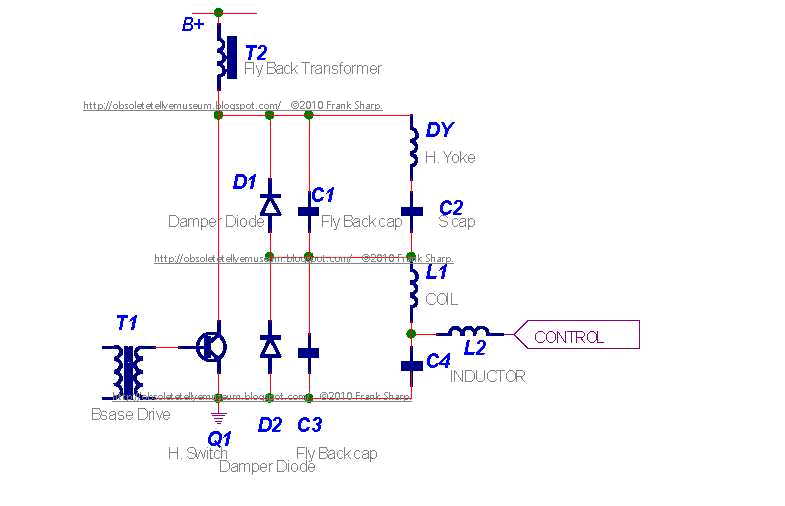 SPLIT DIODE MODULATOR
This horizontal circuit consists of two parts. D1, C1, C2 and DY are the components as described above.
D2, C3, C4 and L1 are a second “dummy” horizontal section that does not cause deflection current. By the
D.C. analyzing this circuit the voltage across C2 + C4 must equal the supply voltage (B+). Deflection
current in the DY is related to the supply voltage minus the voltage across C4. For a maximum horizontal
size the control point must be held at ground. This causes the dummy section to not operate and the DY
section will get full supply voltage. If the control point is at 1/3 supply then the DY section will be
operating at 2/3 supply.
Note: The impedance of (D1,C1,C2 and DY) and (D2,C3,C4 and L1) makes a voltage divider. If the
control point is not connected then there is some natural voltage on C4. Most split diode monitors are built
to pull power from the dummy section through L2 to ground. A single power transistor shunts from the
control point to ground. It is true that power can be supplied from some other supply through L2 to rise the voltage on C4. For maximum range a bi-directional power amplifier can drive the control point.
The most exciting feature if the split diode modulator is that the flyback pulse, as seen by the flyback
transformer, is the same size at all horizontal size settings.
HORIZONTAL SWITCH/DAMPER DIODEOn the right hand side of the screen, the H. switch transistor conducts current through the deflection yoke.
This current comes from the S correction capacitors, which have a charge equal to the effective supply
voltage. The damper diode allows current for the left hand side of the screen to flow back through the
deflection yoke to the S capacitors.
FLYBACK CAPACITOR
The flyback capacitor connects the hot side of the yoke to ground. This component determines the size and
length of the flyback pulse. ‘Tuning the flyback capacitor’ is done to match the timing of the flyback pulse
to the video blanking time of the video signal. The peak flyback voltage on the horizontal switch must be
set to less that 80% if the Vces specification. The two conditions of time and voltage can be set by three
variables (supply voltage, retrace capacitor and yoke inductance) .
S CAPACITOR
The S capacitors corrects outside versus center linearity in the horizontal scan. The voltage on the S cap
has a parabola plus the DC horizontal supply. Reducing the value of S cap increases this parabola thus
reducing the size of the outside characters and increasing the size of the center characters.
S Capacitor value: Too low: picture will be squashed towards edges.
Too high: picture will be stretched towards edges.
By simply putting a capacitor in series with each coil, the sawtooth waveform is
modified into a slightly sine-wave shape. This reduces the scanning speed near the
edges where the yoke is more sensitive. Generally the deflection angle of the electron
beam and the yoke current are closely related. The problem is the deflection angle
verses the distance of movement on the CRT screen does not have a linear effect.
 BASE DRIVE CURRENT
The base drive resistor determines the amount of
base drive. If the transistor is over driven the Vsat
looks very good, but the current fall time is poor.
If the base current is too small the current fall time is very fast. The problem is that the transistor will have many volts across C-E when closed.
The best condition is found by placing the transistor in the heaviest load condition. Adjust the base resistor for the least power consumption then increase the base drive a small amount. This will slightly over drive the base.
BU208(A)
Silicon NPNnpn transistors,pnp transistors,transistors
Category: NPN Transistor, Transistor
MHz: <1 MHz
Amps: 5A
Volts: 1500V
HIGH VOLTAGE CAPABILITY
JEDEC TO-3 METAL CASE.
DESCRIPTION
The BU208A, BU508A and BU508AFI are
manufactured using Multiepitaxial Mesa
technology for cost-effective high performance
and use a Hollow Emitter structure to enhance
switching speeds.
APPLICATIONS:
* HORIZONTAL DEFLECTION FOR COLOUR TV With 110° or even 90° degree of deflection angle.
ABSOLUTE MAXIMUM RATINGS
Symbol Parameter Value Unit
VCES Collector-Emit ter Voltage (VBE = 0) 1500 V
VCEO Collector-Emit ter Voltage (IB = 0) 700 V
VEBO Emitter-Base Voltage (IC = 0) 10 V
IC Collector Current 8 A
ICM Collector Peak Current (tp < 5 ms) 15 A
TO - 3 TO - 218 ISOWATT218
Ptot Total Dissipation at Tc = 25 oC 150 125 50 W
Tstg Storage Temperature -65 to 175 -65 to 150 -65 to 150 oC
Tj Max. Operating Junction Temperature 175 150 150 °C
----------------------------------------------------------------------------------
Audio - Sound Unit (NF BAUSTEIN 29504-004.23)


TDA1905 (SGS) Audio Output


- TUA2000 (SIEMENS) OSC+ MIXER


The TUA 2000-4 is a monolithically integrated circuit and suitable as a tuner for the VHF
range up to 400 Mkz, e.g. for TV tuners.
RF section
Few externa! components
Stable oscillator frequency and amplitude with very low interference radiation
Optimal rejection of oscillator and input frequencies at the IF output due to a decoupled
active ring mixer circuit
High interference voltage resistance
High-impedance mixer input, for symmetrical and asymmetrical connections
IF post-amplifier for the UHF IF signal
IF section
@
Optimal cross-talk rejection
@
Large signal-modulation range
@
Low noise figure with wide minimum over large load-impedance range
Circuit description
The TUA 2000-4 contains a symmetrical mixer input, as well as a multiplicative mixer. The
oscillator amplitude is regulated. All oscillator operating currents and voltages are stabilized,
so that the oscillator’s amplitude and frequency are largely independent of temperature
and operating voltage changes.
The IF amplifier has been provided with a high impedance input.
The output has two open collector connections.
During UHF operation, oscillator and mixer are switched off and the UHF IF input coupling
stage is activated.
RF section
Few external components
Stable oscillator frequency and amplitude with very low interference radiation
Optimal rejection of oscillator and input frequencies at the iF output due to a decoupled
active ring mixer circuit
High interference voltage resistance
High-impedance mixer input, for symmetrical and asymmetrical connections
IF post-amplifier for the UHF IF signa!
IF section
@
Optima! cross-talk rejection
@
Large signal-modulation range
@
Low noise figure with wide minimum over large load-impedance range
Pin description
- “Open collector” output of the IF SAW driver
- “Open collector” output of the IF SAW driver
- Input for external reference voltage
- Low-ohmic collector output to the high reference point of a parallel resonant circuit
- High-ohmic base input to the high reference point of a parallel resonant circuit
- Oscillator signal output for counter connection
- GND
- “Open collector” output of the mixer
- “Open collector” output of the mixer
- Supply voltage
- Asymmetrical IF signal input for the UHF IF signal
- Mixer high-impedance differential input
- Mixer high-impedance differential input
- Switching voltage input for the VHF-UHF switch selection
- Asymmetrical signal input of the IF SAW amplifier
- GND
- TDA5500 (SIEMENS) IF VIDEO
- TBA120T (TELEFUNKEN) IF AUDIO

TBA120T (Siemens) SIF (Sound IF)
- U264B (TELEFUNKEN) PRESCALER (Under the screen in the middle of PCB)
VIDEO + RGB UNIT (FARB BAUSTEIN 29504-005... )
TDA3561A (PHILIPS) Luminance+Chrominance+RGB MATRIX

PAL decoder TDA3561A
GENERAL DESCRIPTION
The PHILIPS TDA3561A is a decoder for the PAL colour television standard. It combines all functions required for the identification
and demodulation of PAL signals.
Furthermore it contains a luminance amplifier, an RGB-matrix and amplifier. These
amplifiers supply output signals up to 5 V peak-to-peak (picture information) enabling direct drive of the discrete output
stages.

The circuit also contains separate inputs for data insertion, analogue as well as digital, which can be used for text display systems (e.g. (Teletext/broadcast antiope), channel number display, etc. Additional to the TDA3560, the
circuit includes the following features:
· The peak white limiter is only active during the time that the 9,3 V level at the output is exceeded.
The start of the
limiting function is delayed by one line period. This avoids peak white limiting by test patterns which have abrupt transitions from colour to white signals.
· The bri
 ghtness
control is obtained by inserting a variable pulse in the luminance
channel. Therefore the ratio of brightness variation and signal
amplitude at the three outputs will be identical and independent of the
difference in gain of the three channels. Thus discolouring due to
adjustment of contrast and brightness is avoided.
ghtness
control is obtained by inserting a variable pulse in the luminance
channel. Therefore the ratio of brightness variation and signal
amplitude at the three outputs will be identical and independent of the
difference in gain of the three channels. Thus discolouring due to
adjustment of contrast and brightness is avoided.· Improved suppression of the internal RGB signals when the device is switched to external signals, and vice versa.
· Non-synchronized external RGB signals do not disturb the black level of the internal signals.
· Improved suppression of the residual 4,4 MHz signal in the RGB output stages.
· Cascoded stages in the demodulators and burst phase detector minimize the radiation of the colour demodulator
inputs.
· High current capability of the RGB outputs and the chrominance output.
APPLICATION INFORMATION
The function is described against the corresponding pin
number.
1. + 12 V power supply
The circuit gives good operation in a supply voltage range
between 8 and 13,2 V provided that the supply voltage for
the controls is equal to the supply voltage for the
TDA3561A. All signal and control levels have a linear
dependency on the supply voltage. The current taken by
the device at 12 V is typically 85 mA. It is linearly
dependent on the supply voltage.
2. Control voltage for identification
This pin requires a detection capacitor of about 330 nF for
correct operation. The voltages available under various
signal conditions are given in the specification.
3. Chrominance input
The chroma signal must be a.c.-coupled to the input.
Its amplitude must be between 55 mV and 1100 mV
peak-to-peak (25 mV to 500 mV peak-to-peak burst
signal).
 All figures for the chroma signals are based on a
colour bar signal with 75% saturation, that is the
burst-to-chroma ratio of the input signal is 1 : 2,25.
4. Reference voltage A.C.C. detector
This pin must be decoupled by a capacitor of about 330
nF. The voltage at this pin is 4,9 V.
5. Control voltage A.C.C.
The A.C.C. is obtained by synchronous detection of the
burst signal followed by a peak detector. A good noise
immunity is obtained in this way and an increase of the
colour for weak input signals is prevented. The
recommended capacitor value at this pin is 2,2 µF.
6. Saturation control
The saturation control range is in excess of 50 dB.
The control voltage range is 2 to 4 V. Saturation control is
a linear function of the control voltage.
When the colour killer is active, the saturation control
voltage is reduced to a low level if the resistance of the
external saturation control network is sufficiently high.
Then the chroma amplifier supplies no signal to the
demodulator. Colour switch-on can be delayed by proper
choice of the time constant for the saturation control
setting circuit.
When the saturation control pin is connected to the power
supply the colour killer circuit is overruled so that the colour
signal is visible on the screen. In this way it is possible to
adjust the oscillator frequency without using a frequency
counter (see also pins 25 and 26).
7. Contrast control
The contrast control range is 20 dB for a control voltage
change from + 2 to + 4 V. Contrast control is a linear
function of the control voltage. The output signal is
suppressed when the control voltage is 1 V or less. If one
or more output signals surpasses the level of 9 V the peak
white limiter circuit becomes active and reduces the out
putsignals via the contrast control by discharging C2 via an
internal current sink.
8. Sandcastle and field blanking input
The output signals are blanked if the amplitude of the input
pulse is between 2 and 6,5 V. The burst gate and clamping
circuits are activated if the input pulse exceeds a level of
7,5 V.
The higher part of the sandcastle pulse should start just
after the sync pulse to prevent clamping of video signal on
the sync pulse. The width should be about 4 µs for proper
A.C.C. operation.
9. Video-data switching
The insertion circuit is activated by means of this input by
an input pulse between 1 V and 2 V. In that condition, the
internal RGB signals are switched off and the inserted
signals are supplied to the output amplifiers. If only normal
operation is wanted this pin should be connected to the
negative supply. The switching times are very short
(< 20 ns) to avoid coloured edges of the inserted signals
on the screen.
10. Luminance signal input
The input signal should have a peak-to-peak amplitude of
0,45 V (peak white to sync) to obtain a black-white output
signal to 5 V at nominal contrast. It must be a.c.-coupled to
the input by a capacitor of about 22 nF. The signal is
clamped at the input to an internal reference voltage.
A 1 kΩ luminance delay line can be applied because the
luminance input impedance is made very high.
Consequently the charging and discharging currents of the
coupling capacitor are very small and do not influence the
signal level at the input noticeably. Additionally the
coupling capacitor value may be small.
11. Brightness control
The black level of the RGB outputs can be set by the
voltage on this pin (see Fig.5). The black level can be set
higher than 4 V however the available output signal
amplitude is reduced (see pin 7). Brightness control also
operates on the black level of the inserted signals.
12, 14, 16. RGB outputs
The output circuits for red, green and blue are identical.
Output signals are 5,25 V (R, G and B) at nominal input
signals and control settings. The black levels of the three
outputs have the same value. The blanking level at the
outputs is 2,1 V. The peak white level is limited to 9,3 V.
When this level exceeded the output signal amplitude is
reduced via the contrast control (see pin 7).
13, 15, 17. Inputs for external RGB signals
The external signals must be a.c.-coupled to the inputs via
a coupling capacitor of about 100 nF. Source impedance
should not exceed 150 Ω. The input signal required for
a 5 V peak-to-peak output signal is 1 V peak-to-peak.
At the RGB outputs the black level of the inserted signal is
identical to that of normal RGB signals. When these inputs
are not used the coupling capacitors have to be connected
to the negative supply.
18, 19, 20. Black level clamp capacitors
The black level clamp capacitors for the three channels are
connected to these pins. The value of each capacitor
should be about 100 nF.
21, 22. Inputs (B-Y) and (R-Y) demodulators
The input signal is automatically fixed to the required level
by mean
s of the burst phase detector and A.C.C.generator which are connected to pin 21 and pin 22. As the
burst (applied differentially to those pins) is kept constant
by the A.C.C., the colour difference signals automatically
have the correct value.
23, 24. Burst phase detector outputs
At these pins the output of the burst phase detector is
filtered and controls the reference oscillator. An adequate
catching range is obtained with the time constants given in
the application circuit (see Fig.6).
25, 26. Reference oscillator
The frequency of the oscillator is adjusted by the variable
capacitor C1. For frequency adjustment interconnect pin
21 and pin 22. The frequency can be measured by
connecting a suitable frequency counter to pin 25.
28. Output of the chroma amplifier
Both burst and chroma signals are available at the output.
The burst-to-chroma ratio at the output is identical to that
at the input for nominal control settings. The burst signal is
not affected by the controls. The amplitude of the input
signal to the demodulator is kept constant by the A.C.C.
Therefore the output signal at pin 28 will depend on the
signal loss in the delay line.
ABLENKUNG 90° 29504-007.21 TDA2594 HORIZONTAL COMBINATIONThe TDA2594 is a monolithic integrated circuit intended for use in colour television receivers.
The circuit incorporates the following functions:
0 Horizontal oscillator based on the threshold switching principle.
0 Phas
 e comparison between sync pulse and oscillator voltage (tp1).
0 Internal key pulse for phase detector (-D) fYP~ ‘I V
V3-1elp-pl WP- 1° V
* Permissible range: 1 t
TDA2653A Vertical deflection circuit
DESCRIPTION
The TDA2653A is a monolithic integrated circuit for vertical deflection in large screen colour television receivers.
The circuit incorporates the following functions:
· Oscillator; switch capability for 50 Hz/60 Hz operation
· Synchronization circuit
· Blanking pulse generator with guard circuit
· Sawtooth generator with buffer stage
· Preamplifier with fed-out inputs
· Output stage with thermal and short-circuit protection
· Flyback generator
· Voltage stabilizers
PINNING
1. Oscillator adjustment
2. Synchronization input/blanking output
3. Sawtooth generator output
4. Preamplifier input
5. Positive supply of output stage
6. Output
7. Flyback generator output
8. Ground
9. Positive supply (VS)
10. Reference voltage
11. Sawtooth capacitor
12. 50 Hz/ 60 Hz switching voltage
13. Oscillator capacitor.
APPLICATION INFORMATION
The function is described against the corresponding pin number
1, 13
. OscillatorThe oscillator frequency is determined by a potentiometer at pin 1 and a capacitor at pin 13.
2. Sync input/blanking output
Combination of sync input and blanking output. The oscillator has to be synchronized by a positive-going
pulse between 1 and 12 V. The integrated frequency detector delivers a switching level at pin 12.
The blanking pulse amplitude is 20 V with a load of 1 mA.
3. Sawtooth generator output
The sawtooth signal is fed via a buffer stage to pin 3. It delivers the signal which is used for linearity control,
and drive of the preamplifier. The sawtooth is applied via a shaping network to pin 11 (linearity) and via a
resistor to pin 4 (preamplifier).
4. Preamplifier input
The DC voltage is proportional to the output voltage (DC feedback). The AC voltage is proportional to the
sum of the buffered sawtooth voltage at pin 3 and the voltage, with opposite polarity, at the feedback
resistor (AC feedback).
5. Positive supply of output stage
This supply is obtained from the flyback generator. An electrolytic capacitor between pins 7 and 5, and a
diode between pins 5 and 9 have to be connected for proper operation of the flyback generator.
6. Output of class-B power stage
The vertical deflection coil is connected to this pin, via a series connection of a coupling capacitor and a
feedback resistor, to ground.
7. Flyback generator output
An electrolytic capacitor has to be connected between pins 7 and 5 to complete the flyback generator.
8. Negative supply (ground)
Negative supply of output stage and small signal part.
9. Positive supply
The supply voltage at this pin is used to supply the flyback generator, voltage stabilizer, blanking pulse
generator and buffer stage.
10. Reference voltage of preamplifier
External adjustment and decoupling of reference voltage of the preamplifier.
11. Sawtooth capacitor
This sawtooth capacitor has been split to realize linearity control.
12. 50 Hz/60 Hz switching level
This pin delivers a LOW voltage level for 50 Hz and a HIGH voltage level for 60 Hz. The amplitudes of the
sawtooth signals can be made equal for 50 Hz and 60 Hz with these levels.
GRUNDIG SUPER COLOR A4205 SERIE S1618 CHASSIS CUC120 GRUNDIG Tuning unit with bandswitch for high frequency receivers
1. Tuning unit with bandswitch for high frequency receivers having potentiometer means for the control of capacity diodes composed of a plurality of parallelly disposed resistance paths on which wipers are moved by means of screw tuning spindle means mounted beside one another in a common housing of insulating material, bandswitch means formed of metal wires associated with each tuning spindle means, said tuning spindle means being joined for rotation with sleeve means simultaneously forming operating knobs which are borne in apertures in the front plate and each sleeve means having an axial flange surface engaging the back side of the front plate about one aperture therein, said flange surface being slightly larger than the cross section of the apertures and tapering conically away from the back side of the front plate.
2. Tuning unit of claim 1 wherein the sleev
e means are joined
telescopically and coaxially with the tuning spindle means, and the
flange surface engages the back side of the front plate when the sleeve
means are in the state wherein they are pulled out of the front plate.3. Tuning unit of claim 1 wherein the ends of the tuning spindle means which are opposite the front plate have each an annular groove into which a spring bracket engages whose bent end is supported against the housing and which has two diametrically disposed spring arms having opposite spring curvature, the said spring arms in each case contacting the opposite axial walls of the groove.
4. Tuning unit of claim 3 wherein the spring bracket rests with its bent end against the housing and the spring arms additionally engage a bracket formed on the housing or an intermediate bracket formed in one piece with the connection soldering lugs.
5. Tuning unit of claim 3 wherein the spring bracket is formed in one piece with the connection soldering lugs and has spring arms curved both in the same direction which engage an axial wall of the annular groove in the spindle and the opposite axial wall rests against a housing wall.
6. Tuning unit of claim 1 wherein the pointers associated with each potentiometer means lie on the one hand in windows associated with each tuning spindle means in the front plate, and on the other hand are rotatably mounted with their ends opposite the front plate in pivot pins on the housing, and the guiding pin of the spindle nuts carried in a longitudinally displaceable manner on each tuning spindle is provided with a slit disposed parallel to the longitudinal axis of the tuning spindle and slides with its peripheral surface resiliently within the slide tract of the pointer.
7. Tuning unit of claim 1 wherein the bandswitches are formed each of a displaceable metal rod which is in working engagement with stationary metal rods common to all bandswitches of a tuning unit, contacting each of them individually.
8. Tuning unit of claim 7 wherein the metal rods are metal wires.
9. Tuning unit of claim 7 wherein the metal rods are stamped metal parts.
10. Tuning unit of claim 7 wherein levers of insulating material are placed on the front ends of the displaceable metal rods and extend through windows which are provided with detents and which are associated with each tuning spindle in the housing front plate, while the opposite ends are held fixedly in the rearward end of the housing, and the displaceable metal rods individually make contact with contact cams on the stationary metal rods, these cams being in an offset array corresponding to the detents in the windows, the corresponding rods extending parallel to the front plate and parallel to one another behind the front plate.
11. Tuning unit of claim 7 wherein insulating material bridges or insulating material slide pieces are inserted between the contact cams of two adjacent, stationary metal rods and within the free space between two such parallel metal rods.
12. Tuning unit of claim 7 wherein the displaceable metal rods have, in the vicinity of their mountings on the housing, an articulation in the form of a vertically disposed flat portion.
The invention relates to a tuning unit with bandswitch for high frequency receivers, especially radio and television receivers, having a potentiometer system for the control of capacity diodes, the said potentiometer system consisting of a plurality of parallel resistance paths along which wiper contacts can be driven by means of screw spindles disposed adjacent one another in a common insulating material housing in which a bandswitch formed of metal rods is associated with each tuning spindle.
In these tuning units, the working voltages of the capacity diodes in the tuning circuits are recorded once a precise tuning to the desired frequency has been performed. A potentiometer tuning system has great advantages over the formerly used channel selectors operating with mechanically adjustable capacitors (tuning condensers) or mechanically adjustable inductances (variometers), mainly because it is not required to have such great precision in its tuning mechanism.
Tuning
units with bandswitches formed of variable resistances and combined
with interlocking pushbuttons controlling the supply of recorded
working voltages to capacity diodes are known. Channel selection is
accomplished by depressing the knobs, and the tuning or fine tuning are
performed by turning the knobs. The resistances serving as voltage
dividers in these tuning units are combined into a component unit such
that they are in the form of a ladderlike pattern on a common
insulating plate forming the cover of the housing in which the tuning
spindles and wiper contacts corresponding to the variable resistances
are housed. The number of resistances corresponds to the number of
channels or frequencies which are to be recorded. The wiper contact
picks up a voltage which, when applied to the capacity diodes
determines their capacitance and hence the frequency of the
corresponding oscillating circuit. The adjustment of the wipers is
performed by turning the tuning spindle coupled to the tuning knob. By
the depression of a button the electrical connection between a contact
rod and a tuning spindle is brought about and thus the selected voltage
is applied to the capacity diodes. Since the push buttons release one
another, it is possible simply by depressing another button to tune to a
different receiving frequency or a different channel, as the case may
be. 
To permit the switching of a number of channels in a certain tuning range, bandswitches for a plurality of tuning ranges, such as UHF and VHF for example, are often provided in the tuning units described above. In the pushbutton tuning unit of the above-named type, the bandswitch consists of a printed circuit board which is fastened on the housing of the tuning unit, and a switch lever which is preset by means of the pushbutton by turning, and is operated by depressing the pushbutton while at the same time selecting the channel.
Where this combination of knobs and pushbuttons is not possible, the selection of the range is accomplished by means of an additional lever which can be set over to select the range.
However, since such tuning units require too many riveting operations when they are assembled, tuning units were later created in which the individual parts in the voltage divider and pushbutton housing were loosely inserted and/or held in place by projections, lugs, hooks or tabs of resilient plastic. In spite of these initial improvements, the bandswitch, especially the one associated with the tuning units, was still technically intricate and very expensive.
THE INVENTION
It is the object of the invention, therefore, to create an additionally improved and simplified tuning unit containing a bandswitch of simple, space-saving and reliably operating design.
In accordance with the invention, this object is accomplished in a tuning unit with bandswitch of the kind described in the beginning by joining the tuning spindles for rotation with sleeves simultaneously forming the control knobs, which are mounted in apertures in the front plate of the housing and have each a flange engaging the back of the front plate around the aperture, the said flange being slightly larger than the aperture and tapering conically away from the back of the front plate.
In further development, the sleeves can be joined telescopically for rotation with the tuning spindles, and the flange is able to engage the back side of the front plate when the sleeve is in the position in which it is drawn out of the front plate. The sleeves constructed in this manner, whose portions projecting from the apertures in the front plate form the control knobs for the tuning spindles, permit easy assembly of the tuning uni
t and at the same time assure positive co-rotation of sleeves and spindles. The sleeves can be pushed from the front side of the front plate through the apertures onto the clutch surfaces of the spindles, this inward pushing being easily accomplished on account of the taper, and the dropping out of the sleeve being prevented by the flange engaging the back of the front plate. If the control knobs project only slightly out of the front plate, they can be operated from the outside by inserting a tool into them. With the telescoping type of coupling, however, it is possible to draw the sleeves or control knobs further outwardly so that they can be rotated by hand without the use of tools.
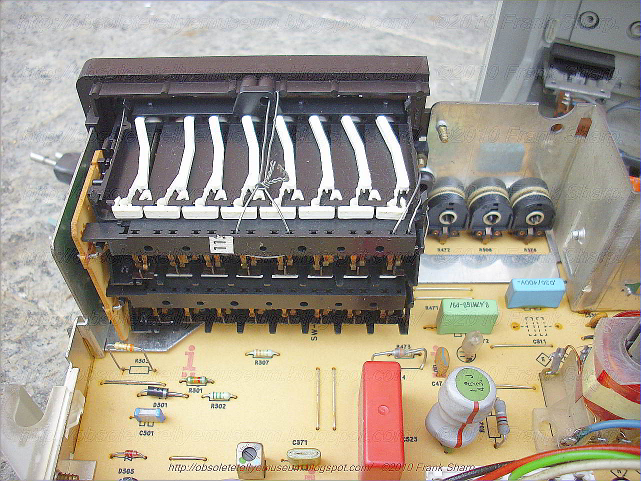
To provide constant assurance of the axial fixation of the tuning spindles, the tuning spindle ends farthest from the front plate can each be provided with an annular groove engaged by a spring bracket whose one leg is supported against the housing and whose other leg is forked to form two spring arms, each bent in the opposite direction and each engaging one of the two opposite walls of the annular groove. The tuning spindles are secured against axial displacement by this construction of the invention alone, without the need for further measures. This facilitates the joining of the sleeves or control knobs to the tuning spindle, because in this case there is no need for precise axial fixation and extreme dimensional accuracy.
Furthermore, the indicators associated with each potentiometer can be mounted in windows in the front plate which are associated with each tuning spindle or tuning knob for visual indication at the front, the other extremities farthest from the front plate being mounted for pivoting on pins set in the housing; the guiding pin on the spindle nut that is driven longitudinally on each tuning spindle can be provided with a slit disposed parallel to the long axis of the tuning spindles and can slide within the indicator slide lever slot, with its surface resiliently engaging the walls of said slot.
In an especially advantageous embodiment, the tuning unit can have bandswitches each formed of a displaceable metal rod which is in contacting engagement individually with stationary metal rods which are common to all of the bandswitches of a tuning unit. It contrast to the bandswitches known hitherto, which as a rule consist of a printed circuit board with switchable contacts thereon, this frequency bandswitch of the invention is of great simplicity, can be manufactured simply and inexpensively, and at the same time is very reliable in operation.
The displaceable and stationary metal rods of the bandswitches can be formed of metal wires or they can be of stamped sheet metal. Also, in further expansion of the concept of the invention, the stationary metal rods thus formed can be all entirely alike and merely offset from one another, thereby further simplifying the manufacture and stocking thereof.
To permit connection also to audiovisual apparatus, one or more of the stationary metal rods can be divided electrically into at least two parts each.
In a special development of this concept, lugs of insulating material can be mounted on the front ends of the displaceable metal wires, these lugs extending through windows in the front plate of the housing which are associated with each tuning spindle and are provided with detents, while the opposite ends can be held fixedly at the rear end of the housing, and the displaceable metal wires can make contact with contact humps on the stationary metal wires, the humps being offset from one another to correspond to the detents in the windows, and the stationary metal wires extending in back of the front plate, parallel to the latter and parallel to one another.
To increase switching reliability, bridges or sliding pieces made of insulating material can be inserted between the contact humps of adjacent stationary wires within the free space between two such parallel lying metal wires.
To
achieve easy displacement of the displaceable metal wires despite the
fixed end mounting on the housing, the displaceable metal wires, in
further embodiment of the invention, can have each an articulation
adjacent their end mountings, in the form of a vertically disposed
flattened portion. This flat permits the metal wires to be deflected
horizontally against a weak spring bias. DESCRIPTION OF THE DRAWING
As an example of the embodiment of the invention, there is represented in the drawings a tuning unit with bandswitch for television receivers. In these drawings,
FIG. 1 is a front elevational view of a tuning unit with bandswitch,
FIG. 2 is a plan view showing the bandswitch of the tuning unit of FIG. 1,
FIG. 3 is a side elevational, cross-sectional view of the tuning unit of FIG. 1,
FIG. 4 is a rear elevational view of the tuning unit of FIG. 1,
FIG. 5 is a plan view showing the indicator means of the tuning unit of FIG. 1,
FIG. 6 shows the sleeve with the operating knob and tuning spindle,
FIG. 7 shows the telescoping manner in which the sleeve is joined to the tuning spindle,
FIG. 8 is a fragmentary view of the bandswitch,
FIG. 9 is another fragmentary view of the bandswitch, and
FIG. 10 shows how the tuning spindle is fixed in position.
DESCRIPTION
The method of representation used in the drawings is greatly simplified, for the purpose of better del
 ineating
the features of the invention. The tuning unit with bandswitch
consists of an insulating material housing 1 with a front plate 2,
which is closed by a cover plate 3 accommodating the resistance paths.
The housing 1 is divided by parallel sidewalls 4 into chambers in which
the tuning spindles 5 are disposed.
ineating
the features of the invention. The tuning unit with bandswitch
consists of an insulating material housing 1 with a front plate 2,
which is closed by a cover plate 3 accommodating the resistance paths.
The housing 1 is divided by parallel sidewalls 4 into chambers in which
the tuning spindles 5 are disposed. The embodiments is an 8-fold tuning unit having eight bandswitches assocated with each tuning spindle, and eight indicators.
Accordingly, there are eight apertures 6 in a central row, through which the operating knobs 7 of the sleeves 8 coupled with the tuning spindles 5 are passed. The operating knobs 7 have recessed surfaces 9 for turning with a turning tool. In a row extending parallel above the row of the apertures 6 there are eight windows 10, whose upper edge is provided with notches 11. Lugs 12 of insulating material extend through the windows 10 and engage the upper notches 11 and are joined behind the front plate to displaceable metal wires 13 of the bandswitch. In a row located beneath the row of apertures 6 another eight windows 14 are provided, through which the ends of the pointers of the indicators 15 protrude.
Now, the bandswitch consists in each case of a displaceable metal wire 13 which can be brought into working engagement with stationary metal wires 16, which are all of the same construction and are only disposed offset from one another. While the displaceable metal wire 13 extends substantially parallel to the longitudinal axis and thus at right angles to the front plate 2, the stationary, parallelly disposed metal wires 16 are parallel to the front plate 2 and are thus inserted at a right angle to the displaceable metal wire. A departure from parallelism or from the right angle, as the case may be, takes place substantially only when the displaceable metal wire 13 is deflected to the two outer notches. The rearward end 18 of the displaceable metal wire, which forms a vertical loop, is tightly inserted into a receiver 17. Just ahead of the loop 18, the metal wire 13 is provided with a vertically disposed portion 19 by a flattening on the metal wire 13. The movement, when the metal wire 13 is deflected into the desired notches or detents, takes place horizontally by the flex
 ing
of these portions 19. The stationary metal wires 16 are held tightly
in their positions in projections 20 on the housing, or by lugs or the
like. Since three switch actions are provided, that is, three ranges,
for each tuning spindle, a bandswitch consists of one displaceable metal
wire and three stationary metal wires 16, which are used for all
switches.
ing
of these portions 19. The stationary metal wires 16 are held tightly
in their positions in projections 20 on the housing, or by lugs or the
like. Since three switch actions are provided, that is, three ranges,
for each tuning spindle, a bandswitch consists of one displaceable metal
wire and three stationary metal wires 16, which are used for all
switches. To permit each bandswitch to have exactly three switching actions, each of the three stationary metal wires 16 has one contact hump 21 corresponding to one of the detents 11 in the windows 10 of the front plate 2. The contact humps 21 are thus located one next to the other as seen from the front plate 2. So that the displaceable metal wire 13 will always come into mechanical and electrical contact only with the desired contact hump, and prevent short circuits, insulating bridges 22 are installed between the adjacent metal wires 16, said insulating bridges being stationary.
If more or less than three switching actions are desired, all that need be done in the case of the bandswitch of the invention is to change the number of stationary metal rods or wires accordingly.
The sleeves 8 with the operating knob 7 have a flange 23 engaging the back of the front plate 2 and tapering back to the point where it joins the tuning spindle. This enables the sleeves to be pushed in, in the case of a housing that has already been manufactured with the tuning spindle installed, without creating the possibility that the sleeves 8 might escape after they have been inserted. The sleeves 8 are connected to the tuning spindles 5 usually by means of driving surfa
 ces.
If manual operation without tools is to be possible, rather than
requiring a tool for the operation of the sleeves, the coupling of the
sleeve 8 to the tuning spindle will be a telescoping coupling (see FIG.
7).
ces.
If manual operation without tools is to be possible, rather than
requiring a tool for the operation of the sleeves, the coupling of the
sleeve 8 to the tuning spindle will be a telescoping coupling (see FIG.
7). The actual firm axial fixation of the tuning spindle 5 is located on the rear end of the housing. Here the tuning spindle 5 has an annular groove 24 which is engaged by a spring by means of two diametrically disposed spring arms 25 and 26. The spring arms 25 and 26 have oppositely curved lugs and are supported on the housing at their terminal and marginal surfaces and their lugs engage opposite axial walls 27 and 28 of the annular groove 24.
Additional support is provided by the common, bent foot 29 of the spring arms 25 and 26 against the cover plate of the housing.
The indic
 ator
means of the tuning unit with bandswitch consists of a pointer 15
which is movable within the window 14, and a cam 30 which is a
prolongation of the pointer 15. At its rearward end, the pointer is
mounted rotatably in the housing on pin 31. Within the cam 30 slides a
guiding pin 32 which is attached to the spindle nut or carriage 40.
Upon the rotation of the tuning spindle, the spindle nut is
longitudinally displaceable therewith. In order to achieve good
guidance and hence precise indication, the guiding pin has a slit 33
extending parallel to the longitudinal axis of the tuning spindle 5, so
that it will resiliently engage the cam 30 within the slot thereof.
ator
means of the tuning unit with bandswitch consists of a pointer 15
which is movable within the window 14, and a cam 30 which is a
prolongation of the pointer 15. At its rearward end, the pointer is
mounted rotatably in the housing on pin 31. Within the cam 30 slides a
guiding pin 32 which is attached to the spindle nut or carriage 40.
Upon the rotation of the tuning spindle, the spindle nut is
longitudinally displaceable therewith. In order to achieve good
guidance and hence precise indication, the guiding pin has a slit 33
extending parallel to the longitudinal axis of the tuning spindle 5, so
that it will resiliently engage the cam 30 within the slot thereof. The necessary soldering lugs are indicated at 34.
On the basis of the design of the tuning unit with bandswitch in accordance with the invention, a desired frequency range--UHF, for example--can be selected by deflecting a displaceable metal wire 13 into one of the detents 11 by means of the lug 12 mounted thereon. Within this range, a transmitter or channel can then be selected by turning the tuning spindle 5. The transmitter preselected in th
 is
manner can then be tuned in by means of a keyboard or by electronic
recall from a keyboard which is not shown. The fine tuning of this
tuned-in transmitter, as well as the selection of a different
transmitter within the same frequency range, is accomplished by turning
the tuning spindle 5.
is
manner can then be tuned in by means of a keyboard or by electronic
recall from a keyboard which is not shown. The fine tuning of this
tuned-in transmitter, as well as the selection of a different
transmitter within the same frequency range, is accomplished by turning
the tuning spindle 5. All of the details explained in the above description and represented in the drawings are important to the invention.
LIST OF FAULTS / COMMON PROBLEMS / THROUBLESHOOTING FOR GRUNDIG CHASSIS CUC120:
Grundig CUC120 Dead - BU208 s/c. Check for C633 ( 100uf ) s/c , R646 , replace C631.
Grundig CUC120 Dead. C633 ( 100u f ) s/c.
Grundig CUC120 FIELD FAULTS C2768 D2761 R2761 6R8 PRESETS OR TDA1770
Grundig CUC120 Frame collapse - sound ok. D2764 ( SKE2F1 ) o/c.
Grundig CUC120 Frame distortion. IC TDA1770 if used , D2761 ( SKE4G1/04 ) , R2761 ( 6.8ohm , .75W )
Grundig CUC120 Int luminance C2527 0µ1 faulty
Grundig CUC120 Interference at sides. IC TDA2595 sync/line osc IC.
Grundig CUC120 Intermittent going into standby. Change R647 to ceramic.
Grundig CUC120 Intermittent shut down. Dry joints on L631 off base of chopper Tx.
Grundig CUC120 Intermittent shut down. IC TDA4600 plus check drys on L631 off base of chopper Tx.
Grundig CUC120 Lack of frame at bottom when cold. C2768 ( 100uf ) on deflection PCB.
Grundig CUC120 No cold start C626 reservoir cap o/c
Grundig CUC120 No luminace. D2536 ( IN4148 ) leaky.
Grundig CUC120 No picture - EHT & sound ok. D2764 ( SKE2F1 ) o/c.
Grundig CUC120 No sound C2408 1000µ s/c; R2408 o/c 3R9 on audio board
Grundig CUC120 Startup - no start up. IC TDA4600 plus check drys on L631 off base of chopper Tx.
Grundig CUC120 Startup - takes a long time to come on. C626 reservoir cap.
No comments:
Post a Comment
The most important thing to remember about the Comment Rules is this:
The determination of whether any comment is in compliance is at the sole discretion of this blog’s owner.
Comments on this blog may be blocked or deleted at any time.
Fair people are getting fair reply. Spam and useless crap and filthy comments / scrapers / observations goes all directly to My Private HELL without even appearing in public !!!
The fact that a comment is permitted in no way constitutes an endorsement of any view expressed, fact alleged, or link provided in that comment by the administrator of this site.
This means that there may be a delay between the submission and the eventual appearance of your comment.
Requiring blog comments to obey well-defined rules does not infringe on the free speech of commenters.
Resisting the tide of post-modernity may be difficult, but I will attempt it anyway.
Your choice.........Live or DIE.
That indeed is where your liberty lies.
Note: Only a member of this blog may post a comment.