


The NORDMENDE (THOMSON) CONTURA 63 (ICC9) CHASSIS ICC9 is a sophisticated chassis which was a unusual engineering technology for a color tv. It doesn't reckon the more standardized schematic reference for a tv. The structure is more oriented in multifunction distributed chipset.

The chassis ICC9 was also fitted and used in models:Telefunken PALcolor 531N, F431, F436M, F531, F531SAT, F536M, F840M, FS535MS, P356M, S259N, S352M, S439, S4400SAT, S440C, S470SL, S480, S539, S5400, S5400SAT, S540C, S540EF, S570SL, Cinevision 10, Cinevision 20, Cinevision 28M, Cinevision 32M, Cinevision 32 Plus
Brandt / Ferguson D51ND, D59F, D59N, D68N, D78N, RP46, S59N, S68N / Nordmende / Saba M5531VT, M6316VT, M6331NIC, M7032NIC, M8500VT, M8510NIC, RP46L, RP52L, SD6325VT, SD7025VT, SD7071, SDM7020, T6349NIC, T6350NIC, T6356S, T7047NIC, T7049VT, T7050NIC, T7052S, T7056NIC, T70K30, T70R30 / Thomson 25DH65J, 28WS72J, 29DF65J, 29DH65J, 29MT52, 63DF68L, 63MT68L, 72DF68L, 72MT68L, 85MX69L, RP52
Micom - 10177330-C9T25
Memory - 24C04CB1
SMPS - TEA2261 & BUH713
TR Chopper - 40-322-35 10117050
Delay - TDA4671
Video - T2160-BK
Color - T-STV2151-AH
Vertical - TDA8172
Sound - TDA2616 & MC33076P1
Stereo - TDA6812-5 & TDA9820
Tuner - MTP-MM-2015-SI
TV/AV - MC14052BCR
TXT - TPU3035 + TMS4C1024DJ
Tube - A68EES038X322 +others types
FBT - 40308-36 10089740NC (HR6463)
HOT - BUH517
RGB Amp. - TEA5101B
remote: - RC1350
IC remote - SAA3008
Other ICs - MV1817-3G CG, HYB514256B-70
ON/OFF - 154V / 130V
NORDMENDE (THOMSON) CONTURA 63 (ICC9) CHASSIS ICC9 Switched mode power supply transformer

A switched mode power supply transformer, particularly for a television receiver, including a primary winding and a secondary winding with the primary winding and the secondary winding each being subdivided into a plurality of respective partial windings. The partial windings of the primary lie in a first group of chambers and the partial windings of the secondary lie in a second group of chambers of a chamber coil body, and the chambers of both groups are nested or interleaved with one another.
1. A switched mode power supply transformer, particularly for a television receiver, comprising in combination:
a primary winding and a secondary winding, with said primary winding being subdivided into three partial windings and said secondary winding being subdivided into two partial windings;
a chamber coil body having a plurality of chambers;
said partial windings of said primary winding being disposed only in a first group of said chambers, and said partial windings of said secondary winding being disposed only in a second group of said chambers, with each of said partial windings being disposed in a respective one of said chambers;
said chambers of said first group being interleaved with said chambers of said second group such that they alternate in sequence with said primary partial windings and said secondary partial windings being alternatingly disposed in five successive said chambers, so as to generate the major operating voltage at said secondary winding; 
an additional secondary winding for generating a further operating voltage, said additional secondary winding likewise being subdivided into a plurality of partial windings; and,
said partial windings of said additional secondary winding are disposed only in respective said chambers of said second group below any of said partial windings of said secondary winding.
2. A transformer as defined in claim 1 wherein the total number of said chambers is six.
3. A transformer as defined in claim 1 wherein the width of the narrowest of said chambers is approximately 1 mm.
4. A transformer as defined in claim 1 or 2 wherein the widths of said chambers are different.
5. A transformer as defined in claim 1 or 2 wherein the total width of all of said chambers is only approximately 20 mm, whereby a flat and optimally coupled transformer is realized.
6. A transformer as defined in claim 1 wherein said additional secondary winding provides an operating voltage for a load which has a fluctuating current input.
7. A transformer as defined in claim 1 wherein said partial windings of said additional secondary winding are connected in parallel.
8. A transformer as defined in claim 1 wherein said partial windings of said primary winding are connected in series.
9. A transformer as defined in claim 1 or 8 wherein said partial windings of said secondary winding are connected in series.
10. A transformer as defined in claim 1 further comprising a plurality of auxiliary primary windings disposed in one chamber of said first group which is disposed in approximately the center of said first group and above the said partial winding of said primary winding disposed in said one chamber of said first group. 
11. A transformer as defined in claim 1 wherein all of said partial winding disposed in said chambers of both said groups are wound with wire having the same diameter.
12. A switched mode power supply transformer as defined in claim 1 or 10 wherein: said coil body has six of of said chambers; said additional secondary winding is subdivided into three said partial windings; and two of said partial windings of said additional secondary winding are disposed below respective ones of said partial windings of said secondary winding and the third said partial winding of said additional secondary winding is disposed in the sixth said chamber.
13. A switched mode power supply transformer as defined in claim 10 further comprising at least one further secondary winding disposed in one of said chambers of said second group above any partial secondary winding present in said one of said chambers.
14. A switched mode power supply transformer, particularly for a television receiver, comprising in combination:
a primary winding and a secondary winding, with said primary winding and said secondary winding each being subdivided into a plurality of partial windings; 
a chamber coil body having a plurality of chambers;
said partial windings of said primary winding being disposed only in a first group of said chambers, and said partial windings of said secondary winding being disposed only in a second group of said chambers with each of said partial windings being disposed in a respective one of said chambers;
said chambers of said first group being interleaved with said chambers of said second group such that said primary partial windings and said secondary partial windings are alternatingly disposed in successive said chambers, so as to generate the major operating voltage at said secondary winding;
an additional secondary winding for generating a further operating voltage, said additional secondary winding likewise being subdivided into a plurality of partial windings, and said partial windings of said additional secondary winding are disposed only in respective said chambers of said second group below any of said partial windings of said secondary winding.
15. A switched mode power supply transformer as defined in claim 1 or 14 wherein each of said partial windings of said primary winding contains the same number of turns and each of said partial windings of said secondary winding contains the same number of turns.
The present invention relates to a switched mode power supply transformer, particularly for a television receiver. 
In communications transmissions devices, particularly in television receivers, it is known to effect the desired dc decoupling from the mains by means of so-called switched mode power supply transformers. Such switched mode power supply transformers are substantially smaller and lighter in weight than a mains transformer for the same power operating at 50 Hz, because they operate at a significantly higher frequency of about 20-30 kHz. Such a switched mode power supply transformer (hereinafter calle
d SMPS transformer) generally includes a primary side with a primary winding serving as the operating winding for the switch and further additional auxiliary windings, as well as a secondary side with a secondary winding for generating the essential operating voltage and possibly further additional windings for generating further operating voltages of different magnitude and polarity. The secondary and primary are insulated from one another as prescribed by VDE and have the necessary dielectric strength so that there is no danger of contact between voltage carrying parts on the secondary. A switched mode power supply (SMPS) circuit for a tv-receiver is described in U.S. Pat. No. 3,967,182, issued June 29, 1976. A further requirement placed on such an SMPS transformer is that the stray inductance at least of the primary winding and of the secondary winding should be as small as possible. With too high a stray inductance, a transient behavior may develop during the switching operation which would not assure optimum switch operation of the switching transistor connected to the primary winding and would endanger this transistor by taking on too much power. Moreover, an increased stray inductance undesirably increases the internal resistance of the voltage sources for the individual operating voltages.
It is known to design the windings for such transformers as layered windings. Such layered windings, however, contain feathered intermediate foil layers and, after manufacture, generally require that the coil or the complete transformer be encased in order to insure VDE safety. Use as a chamber winding in television receivers presently does not take place because of the problems to be discussed below. A chamber winding would have the particular advantage that it could be wound more easily and economically by automatic machines. when using a chamber winding for a switched mode power supply, the detailed insulation between the primary and the secondary would be realized initially by two chambers with one of these chambers being filled only with the windings of the primary and the other of these chambers being filled only with the windings of the secondary. However, with such an arrangement there would exist only slight coupling between the primary and the secondary and thus an undesirably high stray inductance. If, on the other hand, the number of chambers were selected to be substantially larger, the transformer becomes more expensive and unnecessarily large. Moreover, a larger core would be required. Consequently, in the past, no television receiver has been introduced that included an SMPS transformer. SUMMARY OF THE INVENTION
It is the object of the present invention to provide an SMPS transformer designed in the chamber wound technique which permits economical automatic winding, i.e. can be wound with but a single type of wire, has a structure which is spatially narrow and as flat as possible, provides the required insulation between the primary and secondary windings, and has a low stray inductance. The transformer should not be encased or saturated and nevertheless should produce no interfering noise during operation. The transformer should be able to be held in a circuit board without mechanical aids merely by its connecting terminals which are soldered to the circuit board.
The above object is basically achieved according to the present invention in that the transformer for a switched mode power supply, particularly for a television receiver, comprises: a primary winding and a secondary winding with the primary and secondary windings each being subdivided into a plurality of partial windings; and a chamber coil body with a plurality of chambers; and wherein the partial windings of the primary winding are disposed in a first group of chambers of the coil body, the partial windings of the secondary winding are disposed in a second group of chambers of the coil body, and the chambers of the first and second groups are interleaved.
Due to the fact that the individual windings or partial windings of the primary are disposed only in chambers of the first group and the windings or partial windings of the secondary are disposed only in chambers of the second group, i.e. primary and secondary are distributed to separate chambers, the necessary dielectric strength between primary and secondary is assured. By dividing each of the primary and secondary windings to a respective plurality or group of chambers a
nd, due to the interleaved or nested arrangement of the chambers of the primary and the secondary, the desired fixed coupling between primary and secondary, and thus the desired low stray inductance at the primary and secondary, are realized. It has been found that a total number of chambers in the order of magnitude of six constitutes an economically favorable solution. With a smaller number of chambers, the coupling between primary and secondary is reduced. With a larger number of chambers, however, either the individual chambers become too small or the entire transformer, and particularly the core, become too large. 
BRIEF DESCRIPTION OF THE DRAWINGS
FIG. 1 is a circuit diagram for a preferred embodiment of a switched mode power supply transformer according to the invention.
FIG. 2 is a schematic partial sectional view showing the distribution of the individual windings of FIG. 1 to different chambers according to the invention.
DETAILED DESCRIPTION OF THE PREFERRED EMBODIMENT
FIG. 1 shows a transformer intended for a switched mode power supply for a television receiver with a power output between 40 and 150 watts. The transformer includes a primary side P and a secondary side S which, while maintaining the required dielectric strength of, for example, 10,00
0 V, are galvanically decoupled or separated from one another. The primary side P includes a primary winding 1 which, as the operating winding, will lie in the collector circuit of a switching transistor switched at about 20-30 kHz. The primary winding 1 is divided into three partial windings 1a, 1b and 1c which are connected in series. When utilized in a television receiver, the beginning of partial winding 1a and the end of partial winding 1c are connected into the collector circuit of the switching transistor, while the taps between the partial windings 1a-1b and 1b-1c are not utilized, but rather form supporting points for the connection of the terminals of the partial windings. The primary side P also includes an additional winding 3 which feeds the feedback path with which the primary winding 1a-1c is designed as a self-resonant circuit. Moreover, the primary side P includes an additional winding 4 for regulating the moment of current flow in the switching transistor in the sense of stabilizing the amplitude of the output voltages on the secondary side S. The secondary side S initially includes the secondary winding 2 from which is obtained, via a rectifier circuit (not shown), the main operating voltage U1. The secondary winding 2 is divided into two series connected partial windings 2a and 2b. Additionally, the secondary winding S includes a winding 5 for generating an operating voltage for the video amplifier and a further winding 6 for generating the operating voltage for the vertical deflection stage of a television receiver. Moreover, an additional secondary winding 7 is provided from which, after rectification, the operating voltage or the audio output stage of the receiver is obtained. Winding 7 comprises three partial windings 7a, 7b, 7c which are connected in parallel. The audio output stage of a television receiver has a greatly fluctuating current input between 50 mA and 1000 mA so that the load of the secondary side S varies considerably. This variation in load may effect an undesirable change in the operating voltage U1 which also influences the horizontal deflection amplitude. This undesirable dependency can be reduced in that the coupling between winding 7 and winding 4 is dimensioned greater, for regulating purposes, than the coupling between winding 2 and winding 4. This solution is described in greater detail in Federal Republic of Germany Offenlegungsschrift (laid open application) DE-OS No. 2,749,847 of May 10, 1979. This increased coupling between windings 7 and 4 is realized in the present case by the three parallel connected windings 7a, 7b, 7c. Finally, the secondary S includes a further winding 8 which serves to generate, after rectification, a negative operating voltage of -30 V.
FIG. 2 show
s one half of the chamber coil body 9 for the individual windings of FIG. 1, with the body 9 including a total of six chambers 10. The size and particularly the widths of the individual chambers 10 can vary with respect to one another and the widths may all be different. Preferably, the width of the narrowest chamber 10 is about 1 mm and the total width of all six chambers is only approximately 20 mm so as to realize a flat and optimally coupled transformer. As shown, one third of the primary winding 1, in the form of respective partial windings 1a, 1b and 1c, is distributed to each of the first, third and fifth chambers 10 of the coil body 9. The additional primary windings 3 and 4 are disposed in the third chamber 10 above the partial winding 1b. One half of the secondary winding 2, in the form of respective partial windings 2a, 2b, is dis
tributed to each of the second and fourth chambers 10 of the coil body 9. The three partial windings 7a, 7b and 7c of the additional secondary winding 7 for the audio output stage are distributed to the second, fourth and sixth chambers 10, respectively, with the partial windings 7a-7c being disposed closest to the longitudinal axis of the coil body 9 and thus below any partial secondary winding 2a, 2b or other secondary winding which may be located in the same chamber. That is, the partial windings 7a and 7b are disposed below the partial windings 2a and 2b, respectively, in the respective second and fourth chambers 10, and below the additional secondary windings 5 and 8 in the sixth chamber 10. Further winding 6 is disposed above partial secondary winding 2b. As can be seen in FIG. 2, the chambers 10 contain alternatingly only windings or partial windings of the primary side P or of the secondary side S. The illustrated nesting or interleaving of the windings, i.e. the alternating arrangement of windings of the primary side P and of the secondary side S in successive chambers 10, assures the desired close coupling between the primary side P and the secondary side S. The arrangement of the windings 3, 4 in approximately the center of the coil body 9 above partial winding 1b assures the desired close coupling between the windings 3, 4 with the other windings.
In an embodiment of the transformer shown in FIGS. 1 and 2 which was successfully tested in practice, the individual windings were all wound with the same diameter wire and contained the following numbers of turns:
| ______________________________________ |
| Winding No. Number of Turns |
| ______________________________________ |
1a 22 1b 22 1c 22 2a 30 2b 30 3 3 4 10 5 25 6 1 7a 11 7b 11 7c 11 8 16 |
| ______________________________________ |
It will be understood that the above description of the present invention is susceptible to various modifications, changes and adaptations, and the same are intended to be comprehended within the meaning and range of equivalents of the appended claims.
 CRT Line Output Stage Operation Principle:
 I'll examine the operation of the line output stage, whose basic job is to generate a sawtooth current in the line scan coils so that the beams are deflected horizontally across the picture tube's screen. The beams are deflected from the left-hand side to the right-hand side to give the forward line scan: this is followed by a rapid, blanked flyback to the left-hand side ready to trace out the next viewed line. Because of the way in which the flyback is achieved, the line output transformer generates various pulse voltages which are rectified to produce the e.h.t. required by the tube and other supplies. The line output stage is not just any sort of amplifier. The active device, almost always a transistor though valves, thyristors and gate -controlled switches have been used in the past, operates as a switch, the inductive components in the stage being mainly responsible for generating the sawtooth current waveform. Tuning is used to generate and control the flyback. The line drive waveform controls the output transistor's on/off switching and thus determines the timing of the cycle of operations, keeping them phase synchronised with the transmitted picture signal.
Basic Operation
Fig. 1 shows in most basic form the main elements in the line output stage, the active device (transistor) being shown as a switch. When the switch is closed, capacitor C and diode D are shorted out and the 150V supply is connected across coil L. Now it's a basic law of inductance that when a d.c. voltage is connected across a coil the current flowing through the coil builds up linearly from zero. Fig. 2(a) shows this as a positive -going ramp that starts at time t 1 , when the switch is closed. After about 26psec (t2), roughly the time required to deflect the beams from screen centre flows via the large -value capacitor CR, charging the tuning capacitor C with the result that the voltage at its 'upper' plate (the one connected to the coil) rises to a relatively high positive value. When all the energy in coil L has been transferred to capacitor C (time t3) the latter begi
 ns
to discharge, passing the energy back the other way to L via CR which,
as far as the circuit's a.c. operation is concerned, can be regarded as a
short-circuit. At time t4 the capacitor has discharged, having
transferred the energy back to the coil. This to-and-fro interchange of
energy between L and C, which from the a.c. point of view are in
parallel (CR representing a short-circuit), is the normal action of a
tuned/resonant/oscillatory circuit. The resonant frequency is determined
by the values of L and C. These are selected so that when time t4 is
reached, i.e. after a half cycle of oscillation, the sawtooth current
has passed through zero to a negative point on the ramp and the beams
have been deflected to the left-hand side of the screen ready for the
next active line scan. To complete the oscillatory cycle (the normal
resonant circuit action) the voltage at the upper plate of capacitor C
would have to move negatively with respect to chassis. It can't do so
because of the presence of diode D, which is called the efficiency diode
- we'll explain that in a minute. When the voltage at the cathode of D
tries to swing negatively it conducts, i.e. switches on, providing a
discharge path for the coil. Once again because of the inductance in the
circuit there's a gradual, linear current discharge, the enegery being
returned to the supply's reservoir capacitor CR. During this discharge,
the beams are deflected back towards the centre of the screen (times t4
to t5). At this point the magnetic flux (energy) in L has been
dissipated. C is still in its discharged state, being shorted out by
diode D. So at time t5, with the beams at screen centre (zero
deflection), the switch has to be closed so that the cycle of operation
can be repeated. The action of diode D has, with the inductance in the
circuit, provided half the scan power while in the process returning the
energy (minus inevitable circuit losses) to the reservoir capacitor. No
wonder it's called the efficiency diode. It's important to note that
the beam flyback period t2 to t4 is governed by the time -constant of L
and C, consisting of one half cycle of oscillation. To achieve a flyback
time of 12μsec the duration of one cycle needs to be 24μsec: so the
resonant frequency of L and C works out at 41.67kHz. Fig. 3 illustrates
the four phases in the operation of the line output stage. Now the
voltage developed across an inductor is propor- tional to the rate of
change of the current flowing through it. Thus the voltage across L is
relatively low during the forward scan period but correspondingly high
during the flyback, when the current flow is faster because of the
circuit resonance. The voltage developed at the positive plate of
capacitor C is shown in Fig. 2(b), typically peaking at 1,200V. Both the
line output transistor and the efficiency diode must be capable of
withstanding this high reverse voltage. As we've seen, the circuit
action is highly efficient as the energy stored in L is returned to the
supply during the first half of the forward scan: indeed with 'perfect'
components there would be no net demand on the power supply at all! In
practice because of the resistance of the inductor and the losses in the
diode, switch and capacitor the circuit takes out a little more than it
puts back, while the practice of loading the transformer with rectifier
circuits to provide power for other sections of the set increases the
stage's current demand. To make up for these losses, the line output
transistor is switched on slightly before instead of at the centre of
the forward scan. In a practical circuit L is the primary winding of the
line output transformer and the deflection coils are connected across
it via a d.c. blocking capacitor, CB, as shown in Fig. 4. This coupling
capacitor also provides scan -correction (often referred to as S
-correction). Why is this required? If a linear deflection current was
used to control the scanning with a relatively flat -faced picture tube
the sides of the picture would be stretched out in comparison with the
centre section. Hence S -correction: the value of the coupling capacitor
is chosen so that it resonantes with the inductance of the scan coils
at about 5kHz. This has the effect of adding a sinewave component to the
sawtooth current, as shown in
Fig. 5. Thus the deflection power is tailored to suit the length of the
beam paths as the screen is scanned, correcting the horizontal
linearity of the display. At the line scanning frequency the scan coils
behave as an almost perfect inductor, but their small d.c. resistance is
in series with the fixed voltage that should be present across the
coil. It has the effect of introducing an asymmetric sensitivity loss
during the forward scan. To counteract it a further component is added
in series with the scan coils - an inductor with a saturable magnetic
core, biased by a permanent magnet so that its inductance falls as the
scan current increases. The voltage drop across this inductor, which is
known as the linearity coil, varies in the opposite sense to that
produced by the resistance of the coils, thus providing an equal -but
-opposite cancellation effect. In some TV sets the permanent magnet can
be adjusted to trim the linearity correction, though many modern sets
use components with such tight tolerances that a sealed linearity
-correction coil can be used. With some very small -screen sets the
horizontal non -linearity effect is small enough to be ignored.
ns
to discharge, passing the energy back the other way to L via CR which,
as far as the circuit's a.c. operation is concerned, can be regarded as a
short-circuit. At time t4 the capacitor has discharged, having
transferred the energy back to the coil. This to-and-fro interchange of
energy between L and C, which from the a.c. point of view are in
parallel (CR representing a short-circuit), is the normal action of a
tuned/resonant/oscillatory circuit. The resonant frequency is determined
by the values of L and C. These are selected so that when time t4 is
reached, i.e. after a half cycle of oscillation, the sawtooth current
has passed through zero to a negative point on the ramp and the beams
have been deflected to the left-hand side of the screen ready for the
next active line scan. To complete the oscillatory cycle (the normal
resonant circuit action) the voltage at the upper plate of capacitor C
would have to move negatively with respect to chassis. It can't do so
because of the presence of diode D, which is called the efficiency diode
- we'll explain that in a minute. When the voltage at the cathode of D
tries to swing negatively it conducts, i.e. switches on, providing a
discharge path for the coil. Once again because of the inductance in the
circuit there's a gradual, linear current discharge, the enegery being
returned to the supply's reservoir capacitor CR. During this discharge,
the beams are deflected back towards the centre of the screen (times t4
to t5). At this point the magnetic flux (energy) in L has been
dissipated. C is still in its discharged state, being shorted out by
diode D. So at time t5, with the beams at screen centre (zero
deflection), the switch has to be closed so that the cycle of operation
can be repeated. The action of diode D has, with the inductance in the
circuit, provided half the scan power while in the process returning the
energy (minus inevitable circuit losses) to the reservoir capacitor. No
wonder it's called the efficiency diode. It's important to note that
the beam flyback period t2 to t4 is governed by the time -constant of L
and C, consisting of one half cycle of oscillation. To achieve a flyback
time of 12μsec the duration of one cycle needs to be 24μsec: so the
resonant frequency of L and C works out at 41.67kHz. Fig. 3 illustrates
the four phases in the operation of the line output stage. Now the
voltage developed across an inductor is propor- tional to the rate of
change of the current flowing through it. Thus the voltage across L is
relatively low during the forward scan period but correspondingly high
during the flyback, when the current flow is faster because of the
circuit resonance. The voltage developed at the positive plate of
capacitor C is shown in Fig. 2(b), typically peaking at 1,200V. Both the
line output transistor and the efficiency diode must be capable of
withstanding this high reverse voltage. As we've seen, the circuit
action is highly efficient as the energy stored in L is returned to the
supply during the first half of the forward scan: indeed with 'perfect'
components there would be no net demand on the power supply at all! In
practice because of the resistance of the inductor and the losses in the
diode, switch and capacitor the circuit takes out a little more than it
puts back, while the practice of loading the transformer with rectifier
circuits to provide power for other sections of the set increases the
stage's current demand. To make up for these losses, the line output
transistor is switched on slightly before instead of at the centre of
the forward scan. In a practical circuit L is the primary winding of the
line output transformer and the deflection coils are connected across
it via a d.c. blocking capacitor, CB, as shown in Fig. 4. This coupling
capacitor also provides scan -correction (often referred to as S
-correction). Why is this required? If a linear deflection current was
used to control the scanning with a relatively flat -faced picture tube
the sides of the picture would be stretched out in comparison with the
centre section. Hence S -correction: the value of the coupling capacitor
is chosen so that it resonantes with the inductance of the scan coils
at about 5kHz. This has the effect of adding a sinewave component to the
sawtooth current, as shown in
Fig. 5. Thus the deflection power is tailored to suit the length of the
beam paths as the screen is scanned, correcting the horizontal
linearity of the display. At the line scanning frequency the scan coils
behave as an almost perfect inductor, but their small d.c. resistance is
in series with the fixed voltage that should be present across the
coil. It has the effect of introducing an asymmetric sensitivity loss
during the forward scan. To counteract it a further component is added
in series with the scan coils - an inductor with a saturable magnetic
core, biased by a permanent magnet so that its inductance falls as the
scan current increases. The voltage drop across this inductor, which is
known as the linearity coil, varies in the opposite sense to that
produced by the resistance of the coils, thus providing an equal -but
-opposite cancellation effect. In some TV sets the permanent magnet can
be adjusted to trim the linearity correction, though many modern sets
use components with such tight tolerances that a sealed linearity
-correction coil can be used. With some very small -screen sets the
horizontal non -linearity effect is small enough to be ignored.Practical Line Output Stage

Fig. 6 shows a relatively simple line output stage circuit used with a 90° -deflection tube. Tr5 is the line output transistor, which incorporates the efficiency diode in the same package. The primary winding of the line output trans- former T4 is the section between pins 2 and 10, C95 being the flyback tuning capacitor. Scan coil coupling and S - correction are provided by C94, the line linearity coil L14 being connected in series on the chassis side of the scan current path. L14 is damped by R110 to prevent it ringing when the line flyback pulse occurs - the effect of an undamped linearity coil is velocity modulation of the beams at the beginning of their sweeps, showing up as black -and - white vertical striations at the left-hand side of the screen. C92 is the reservoir capacitor, the h.t. feed being via 8105. 8106 and R109 feed pulses to the second phase -locked loop (APC2) in the sync chip - we dealt with this in last month's instalment. A second pulse feed from the same point goes to the colour decoder chip to provide line blanking, burst gating and PAL switch drive - this particular set doesn't use the sandcastle pulse approach.
Secondary Supplies
So much for the generation and control of the sawtooth scanning current. The rest of the components in this circuit are used to harness the energy in the transformer to provide power supplies for other sections of the receiver. The winding between pins 4 and 8 pulse energises the picture tube's heaters at 6.3V r.m.s. The other supplies make use of the transformer as the heart of a d.c.-to-d.c. converter system, by means of secondary windings that provide pulse feeds to diode/capacitor rectifier circuits. Small -value (0.680) resistors in the 25V and 200V supplies provide surge limiting and protection (by going open -circuit) in the event of a short-circuit in one of these supplies. The most significant supply is obtained from the diode - split winding that starts at pin 9. Although not shown in full detail it consists of several 'cells', each of which consists of an electrically isolated secondary winding, a built-in high - voltage rectifier diode and, as the reservoir capacitor, the carefully contrived capacitance that's present between adjacent, highly -insulated winding layers. These cells are connected in series to form a voltage -multiplier system capable of providing an e.h.t. supply for the tube's final anode of typically 24kV - it may be as high as 30kV in some designs. There's a built-in surge limiter resistor at the output end of the chain of cells. An important part of the e.h.t. multiplier system is the final reservoir capacitor that split chain provides about 8kV to a built-in potential -divider chain that contains two pres
ets:
the one at the top provides the supply for the tube's focus electrode
while the one near the bottom provides its first anode supply of about
800V. The bottom of the diode -split chain (pin 9) is returned to
chassis via a diode/capacitor/resistor network (not shown here). The
voltage developed across this network is proportional to the total beam
current, since this flows from the tube's cathodes via the e.h.t.
connector and the diode -split chain to chassis. Above a certain
threshold the voltage at pin 9 reduces the picture brightness and/or
contrast via the colour decoder/matrixing chip, limiting the beam
current and hence the dissipation in the tube's shadowmask to safe
levels. The winding between pins 10 and 7 of the transformer produces
50-70V pulses that sit on the h.t. voltage present at pin 10. When
rectified by D23 and C100 a 200V supply is provided for the RGB output
stages that drive the tube's cathodes. Secondary winding 4-6 feeds D24
and C99 which provide a 25V supply for the field timebase. In some
designs supplies for the audio output stage and the signal sections of
the receiver are also obtained from the line output transformer: in this
particular chassis they are obtained from the chopper transformer in
the power supply instead. Incidentally there have been one or two
designs, the Ferguson/philco TX10 chassis being a well-known example,
where the e.h.t. is also obtained from the chopper transformer, the line
output transformer then acting mainly as a load for the line output
transistor. In earlier designs a separate diode - capacitor multiplier
unit (tripler) was fed from a single line output transformer overwiding
to provide the e.h.t.Scan Rectification
The e.h.t., focus and 200V supplies d
erived
from the transformer are relatively lightly loaded, i.e. no great
current demand is placed on them. They can therefore be obtained by
rectifying the pulses present during the flyback period (time t2 -t4 in
Fig. 2), which is about twenty per cent of the scan cycle. Where the
current demand is greater, e.g. in a supply for the field timebase or an
audio output stage, the phasing of the relevant transformer winding is
often arranged so that the rectifier diode conducts during the scan
rather than the flyback period. Although the voltage available is much
lower, it's present for a longer period (about eighty per cent of the
scan/duty cycle). As a result the output regulation is much better. The
relatively high peak reverse voltage has to be taken into account in the
rectifier diode's specification.EHT Regulation
The internal impedance of a diode -sp
lit
e.h.t. supply is typically about 1MOhm. Thus with a total beam current
of lmA, present when a bright picture is being displayed on a 22in.
picture tube, the e.h.t. voltage will drop by about 1kV or five per
cent. The result of this is some ballooning, i.e. increase in picture
size. Compensation can be provided by reducing the line scanning power.
Careful choice of the value of the resistor that feeds the line output
transformer - R105 in Fig. 6 - gives automatic compensation in the
horizontal direction, while deriving the supply for the field output
stage from the line output transformer tends to cancel out the
ballooning in the vertical plane. Various 'anti -breathing' arrangements
are used in TV receiver design. Most operate via the diode -modulator
circuit we'll come to shortly. With any line output stage circuit the
picture width and e.h.t. voltage depend on the stage's h.t. supply, so
this must be well regulated and set up correctly. In the circuit shown
in Fig. 6 the h.t. voltage has to be 119V with a 20in. tube and 145V
with a 22in. tube.Pincushion Distortion
The raster produced on an almost -flat faced picture tube by constant -amplitude scan currents has pincushion distortion at all four sides. This is because of the disparity between the image plane and the screen's profile - . As a general rule the deflection yokes used with modern 90° tubes have built-in correction for both NS (vertical) and EW (horizontal) pincushion distortion while 110° tubes (generally above 22in. screen size) have in -yoke correction for NS distortion but cannot fully compensate for the
 pincushion
effect at the sides of the screen. Thus with these the line scan
current has to be amplitude -modulated by a parabolic waveform at field
frequency as shown in Fig. 7. With present-day tube designs a modulation
depth of about seven per cent is required. the peak -to -peak scan
current being typically 4.1A at the top and bottom of the screen and
4.4A towards the centre of the screen, where the deflection power is
greatest. Amplitude modulation of the line scan current can be achieved
by including a saturable -reactance transformer in series with the scan
coils, but this is expensive. You could put a suitably -shaped ripple on
the supply to the line output stage, but the parabola would be
superimposed on any secondary supplies derived from the line output
transformer. The most widely used solution is to employ a diode -modu-
lator circuit, since this gives full control of the raster shape and
scan amplitude while providing a constant load current and flyback time.
pincushion
effect at the sides of the screen. Thus with these the line scan
current has to be amplitude -modulated by a parabolic waveform at field
frequency as shown in Fig. 7. With present-day tube designs a modulation
depth of about seven per cent is required. the peak -to -peak scan
current being typically 4.1A at the top and bottom of the screen and
4.4A towards the centre of the screen, where the deflection power is
greatest. Amplitude modulation of the line scan current can be achieved
by including a saturable -reactance transformer in series with the scan
coils, but this is expensive. You could put a suitably -shaped ripple on
the supply to the line output stage, but the parabola would be
superimposed on any secondary supplies derived from the line output
transformer. The most widely used solution is to employ a diode -modu-
lator circuit, since this gives full control of the raster shape and
scan amplitude while providing a constant load current and flyback time.The Diode Modulator

Fig. 8 shows the essence of a diode -modulator arrange- ment. The efficiency diode is split in two, DI and D2, which perform the same clamping action as before. The flyback tuning capacitor is also split in two, Cl and C2: the upper one tunes the transformer and scan coils (L1) as before while the lower one tunes a bridge coil, L2, via C4 to the same flyback frequency of about 42kHz. C3 is the scan coupling capacitor, which corresponds with CB in Fig. 4. Modulation is achieved by using transistor Tr2, whose conduction governs the scan width, to vary the load across C4. When Tr2 is off, the scan energy is shared between the the two series LC combinations C3/L1 and L2/C4. The charge on C3 and C4 is in the ratio of about 7:1, the scan current being reduced in proportion. When Tr2 is fully conductive, C4 is effectively shorted out and acquires no charge. Thus a greater proportion of the energy is present in C3/L1 and the scan current and picture width are increased. By varying the conduction of Tr2 during the forward scan in a parabolic manner, EW pincushion correction is achieved. The basic picture width can be controlled by varying Tr2's standing bias. Choke L3 and the large -value capacitor
C5
filter the line -frequency energy so that it doesn't reach Tr2. And
because both sections of the load (L 1/C1 and L2/C2) are individually
tuned to the flyback frequency the flyback time, and hence the e.h.t.
and the other line output transformer -derived supplies, remain constant
over the field period despite the line scan current variation. There
are several different versions of the diode -modu- lator arrangement.
Some tube/yoke combinations have a scan -geometry characteristic such
that when the line scan current is modulated by a simple parabolic
waveform as described above the raster has inner pincushion distortion
as shown in Fig. 9.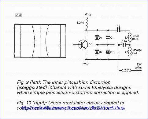 Because
of this. the EW-correction system also has to modulate the S
-correction. Fig. 10 shows, in skeleton circuit form. how this can be
done. There are two coupling/S-correction capacitors. C3 and C3A. C3 is
the usual S -correction capacitor, but C3A has an increasing influence
as the diode modulator begins to have maximum effect towards the centre
of the screen. Critical choice of the value of C3A ensures that the
inner curved verticals shown in Fig. 9 are straightened out to give a
raster completely free from geometric distortion. Although all diode
modulators work on the same basic principle, in some designs a
transformer is used in place of the bridge coil to give better impedance
matching and balance. Fig. 11 shows such an arrangement, used by Bang
and Olufsen. The EW correction waveform is applied to transformer T6.
whose winding 1-2 takes the place of L2 in Figs. 8 and 10. This circuit
also provides inner -pincushion distortion correction as just described,
the supplementary S - correction capacitor being C36.
Because
of this. the EW-correction system also has to modulate the S
-correction. Fig. 10 shows, in skeleton circuit form. how this can be
done. There are two coupling/S-correction capacitors. C3 and C3A. C3 is
the usual S -correction capacitor, but C3A has an increasing influence
as the diode modulator begins to have maximum effect towards the centre
of the screen. Critical choice of the value of C3A ensures that the
inner curved verticals shown in Fig. 9 are straightened out to give a
raster completely free from geometric distortion. Although all diode
modulators work on the same basic principle, in some designs a
transformer is used in place of the bridge coil to give better impedance
matching and balance. Fig. 11 shows such an arrangement, used by Bang
and Olufsen. The EW correction waveform is applied to transformer T6.
whose winding 1-2 takes the place of L2 in Figs. 8 and 10. This circuit
also provides inner -pincushion distortion correction as just described,
the supplementary S - correction capacitor being C36.Diode Modulator Drive

The parabolic EW drive waveform required is easily obtained by feeding the field -scan sawtooth waveform to a double integrator. By adding a sawtooth component the shape of the parabolic waveform can be tilted in either direction to give keystone -distortion correction if required - this is not generally necessary with modern tube/yoke designs. These EW correction characteristics are adjustable by preset resistors or, in the case of bus -programmable sets, remote control commands to the deflection processor. Very often the EW modulator is used to correct the previously mentioned picture breathing effect: this is done by feeding to the EW modulator's control circuit a voltage that's proportional to beam current.
NORDMENDE (THOMSON) CONTURA 63 (ICC9) CHASSIS ICC9 Raster distortion correction circuitry Unit for a video display apparatus that includes a square-planar picture tube
 -planar picture tube, that includes a phosphor screen located on a faceplate having an aspherically curved geometry that produces a relatively flat surface contour. Deflection circuitry generates line and field scanning currents in respective line and field deflection windings to enable the electron beams of the picture tube to scan a raster on the phosphor screen. The electron beams are subject to a scanning error that results in raster distortion, such as side pincushion distortion. A parabola generator produces a parabolic modulation of the scanning of the electron beams to generally correct the raster distortion while retaining a residual error due to the aspherically curved geometry of the faceplate. A nonlinear waveshaping circuit modifies the parabolic modulation of the scanning current in accordance with the aspherically curved geometry to provide additional modulation of the electron beam scanning for correcting the residual error. The nonlinear waveshaping circuit includes a current source and a switched current divider that is responsive to a threshold level of the parabolic voltage developed by the parabola generator.
This version is realized with the feature of an IC, principles of the means are almost the same.
1. Video display apparatus with correction of raster distortion, comprising:
a picture tube having a phosphor screen located on a faceplate having an aspherically curved surface contour, with at least one of a minor and major axis exhibiting a curvature that changes from an edge of the faceplate to the center;
deflection means including horizontal and vertical deflection windings for generating respectively therein horizontal and vertical deflection currents to enable an electron beam of said picture tube to scan a raster on said phosphor screen;
a parabola generator coupled to said deflection means for generating a generally parabolically shaped signal that produces a parabolic modulation of the scanning of said electron beam to generally provide correction of a first raster distortion while leaving uncorrected a residual raster distortion due to the change in curvature of said faceplate from said edge to the center; and
means for nonlinearly modifying said (parabolic modulation) parabolically shaped signal as a function of said change in curvature of said faceplate to provide additional modulation of the scanning of said electron beam for correcting said residual raster distortion.
2. Apparatus according to claim 1 wherein said first raster distortion results in side pincushion raster distortion and wherein said faceplate has an aspherically curved geometry that results in areas of said faceplate near the top and bottom being of increased curvature relative to the curvature in areas near the center. 3. Apparatus according to claim 2 wherein said residual raster distortion comprises a barrel-like distortion of a raster display of a vertical line pattern in said areas near the top and bottom of said faceplate. 4. Apparatus according to claim 2 wherein said nonlinearly modifying means comprises a current source coupled to said parabola generator and a switched current divider that switches from a first conductive state to a second conductive state during that portion of a vertical trace interval when a raster is being scanned on said faceplate in said areas of increased curvature. 5. Apparatus according to claim 4 wherein said parabolically shaped signal is a generally parabolically shaped input voltage repeating at a vertical deflection rate and having both a DC component voltage and an AC parabolic component voltage and wherein said switched current divider comprises an impedance receiving a constant current from said current source for establishing a bias voltage level and switching means responsive to said bias voltage level and direct current coupled to said parabola generator for shunting a portion of said constant current when said input voltage goes beyond a threshold voltage level established in accordance with said bias voltage level to modify the waveshape of said input voltage in a manner that corrects said residual raster distortion. 6. A circuit for correcting a
given error of electron beam positioning in a video display apparatus, comprising: a deflection winding;
an output stage for generating current in said deflection winding to control said electron beam positioning;
a parabolic voltage generator for developing a generally parabolically shaped input voltage repeating at a deflection rate and having both a DC component voltage and an AC parabolic component voltage;
an amplifier for driving said output stage in accordance with said parabolically shaped input voltage to generally correct said given error while retaining a residual error of said electron beam positioning;
a current source;
an impedance receiving current from said current source for establishing a bias voltage level; and
switching means responsive to said bias voltage level and direct current coupled to said parabolically shaped input voltage for shunting a portion of the current from said current source when said input voltage goes beyond a threshold voltage level established in accordance with said bias voltage level to modify the waveshape of said input voltage in a manner that corrects said residual error.
7. A circuit according to claim 6 wherein said switching means is direct current coupled to an output terminal of said parabolic voltage generator, at which terminal said input voltage is developed, and which is direct current coupled to a terminal of said impedance, at which impedance terminal said bias voltage level is developed. 8. A circuit according to claim 7 wherein said switching means comprises a diode in which there flows the shunted portion of current from said current source. 9. A circuit according to claim 7 wherein the shunted portion of current from said current source establishes a modified parabola voltage at an output terminal of said switching means that is direct current coupled to the output terminal of said parabolic voltage generator, said modified parabola voltage having a waveform that generally follows the waveform of said input voltage when said switching means is in one conductive state and having a waveform of waveshape that is substantially different than that of said input voltage when said switching means is in another conductive state. 10. A circuit according to claim 9 including means for AC coupling said modified parabola voltage to said amplifier. 11. A circuit according to claim 10 including means for adjusting said bias voltage level to adjust the switching instants of said switching means and wherein a peak amplitude of said modified parabola voltage remains substantially unchanged for different adjustments of said bias voltage level. 12. A circuit according to claim 11 including an adjustable voltage divider coupled to said AC coupling means and direct current coupled to said amplifier for adjusting the amplitude of the AC coupled modified parabola voltage, and wherein the peak amplitude of the modified parabola voltage that is established at the output terminal of said switching means remains substantially unchanged for different adjustments of said voltage divider. 13. A circuit according to claim 9 wherein said input voltage includes an AC sawtooth component voltage repeating at said deflection rate and further including means for applying said sawtooth component voltage to said impedance to provide common-mode rejection of said sawtooth component voltage with respect to the shunted portion of current from said current source. 14. A circuit according to claim 9 wherein said switching means applies an additional voltage to said terminal of said impedance that is representative of the difference between said bias voltage level and said input voltage to control the amplitude of the shunted portion of current in accordance with said additional voltage. 15. A circuit according to claim 9 wherein said current source comprises a source of DC voltage coupled to a second impedance, and wherein said switching means applies an additional voltage to said terminal of the first mentioned impedance that is representative of a difference between said bias voltage level and said input voltage. 16. A circuit according to claim 15 wherein said DC voltage of said DC voltage source is substantially greater in magnitude than that of said additional voltage to prevent significant changes from occurring in the magnitude of said current source when said switching means changes conductive states. 17. A circuit according to claim 6 wherein said video display apparatus includes a picture tube having a phosphor screen located on a faceplate having an aspherically curved geometry that produces a relatively flat surface contour and wherein said residual error of electron beam positioning is produced in accordance with said aspherically curved geometry. 18. A circuit according to claim 17 wherein said given error is produced by side pincushion distortion and wherein said residual error produces a barrel-like distortion of a raster display of a vertical line pattern in regions near the top and bottom of said faceplate where the curvature of said faceplate is increased relative to the curvature in the center region. 19. Apparatus according to claim 1 wherein said nonlinearly modifying means produces a parabolic modulation when scanning raster lines near top and bottom of said raster that is different than when scanning raster lines near raster center for correcting said residual raster distortion due to the aspherically curved geometry of said faceplate. New, flatter faceplate picture tubes, such as the RCA Corporation square-planar picture tubes, have aspherically curved faceplate contours. A tube of this type, having a complex curvature faceplate, is described in the following U.S. patent applications, herein incorporated by reference.
1. U.S. patent application Ser. No. 469,772, filed Feb. 25, 1983, by F. R. Ragland, Jr. entitled CATHODE-RAY TUBE HAVING AN IMPROVED SHADOW MASK CONTOUR.
2. U.S. patent application Ser. No. 469,774, filed Feb. 25, 1983 by F. R. Ragland, Jr. entitled CATHODE-RAY TUBE HAVING A FACEPLATE PANEL WITH A SUBSTANTIALLY PLANAR PERIPHARY.
3. U.S. patent application Ser. No. 469,775, filed Feb. 25, 1983, by R. J. D'Amato et al., entitled CATHODE-RAY TUBE HAVING DIFFERENT CURVATURE ALONG MAJOR AND MINOR AXES.
4. U.S. patent application Ser. No. 529,644, filed Sept. 6, 1983, by R. J. D'Amato et al., entitled CATHODE-RAY TUBE HAVING A FACEPLATE PANEL WITH AN ESSENTIALLY PLANAR SCREEN PERIPHERY.
In one form of flatter faceplate picture tube, as typified by the RCA 110° COTY-SP, square-planar, 27 V, color television picture tube, A68ACC10X, the formula for the tube faceplate sagittal height, z, in millimeters, with reference to the center of the faceplate is given by: Z=A 1 X 2 +A 2 X 4 +A 3 Y 2 +A 4 X 2 Y 2 +A 5 X 4 Y 2 +A 6 Y 4 +A 7 X 2 Y 4 +A 8 X 4 Y 4 ,
where X and Y are the distance coordinates, in millimeters, from the faceplate center along the major and minor axes, respectively, and where: A 1 =-0.236424229×10 -4 A 2 =-0.363538575×10 -8 A 3 =-0.422441063×10 -3 A 4 =-0.213537355×10 -8 A 5 =+0.883912220×10 -13 A 6 =-0.100020398×10 -9 A 7 =+0.117915353×10 -14 A 8 =+0.527722295×10 -21
The picture tube faceplate defined by this formula has a relatively shallow curvature near the center of the faceplate, which increases near the edges along paths parallel to both the major and minor axes of the tube. The overall result is a faceplate of relatively flat appearance and with planar edges, namely, with points along the top, bottom, right and left edges located substantially in a common plane.
In general, the raster scanned on the phosphor screen of a picture tube may exhibit an east-west or side pincushion raster distortion. This distortion may be substantially corrected by a side pincushion correction circuit that produces a parabolic amplitude modulation of the horizontal deflection current. The required vertical rate parabola voltage may be obtained from the vertical deflection circuit by integration of the vertical sawtooth current.
When using such a conventional circuit for raster correction in a picture tube, such as a square-planar picture tube that has an aspherically curved faceplate, a small but often objectionable raster distortion may remain at the top and bottom of the display, as illustrated by the solid vertical lines of a raster R display R in FIG. 1. Due to the aspherically curved geometry of the faceplate, the vertical line bend away from the vertical direction near the top and bottom of the raster display, where the curvature of the faceplate increases. The overall appearance of the vertical lines in FIG. 1 is slightly barrel-shaped.
In accordance with an aspect of the invention, a video display apparatus includes a picture tube having a phosphor screen located on a faceplate having an aspherically curved geometry. Correction circuitry is provided that compensates for raster distortion or electron beam positioning errors, such as pincushion or convergence distortions. The correction circuitry includes a parabola generator coupled to deflection circuitry for producing a parabolic modulation of the scanning of the electron beam. The modulation generally provides correction of the raster distortion or electron beam positioning error, while retaining a residual error due to the aspherically curved geometry of the faceplate. The modulation is nonlinearly modified in accordance with the aspherically curved geometry to provide additional modulation of the scanning of the electron beam for correcting the residual error. In accordance with another aspect of the invention, a particularly advantageous arrangement of correction circuitry smoothly straightens the bent vertical lines near the top and bottom of the raster display illustrated in FIG. 1.
The parabola generator of the correction circuit arrangement produces a generally parabolically shaped input voltage repeating at a deflection rate. An amplifier drives an output stage that generates current in a deflection winding to control the electron beam landing position. The amplifier is responsive to the output of the parabola generator for driving the output stage in accordance with the parabolically shaped input voltage to generally correct electron beam landing error, while retaining a residual error. A current source with a switched current dividing network is responsive to a threshold level of the parabolically shaped input voltage for supplying to the amplifier a portion of the current from the current source when the input voltage exceeds the threshold level to correct the residual error. FIG. 1 illustrates vertical lines of a raster display scanned on the screen of a square-planar picture tube;
FIG. 2 illustrates in block diagram form raster scanning circuitry used in conjunction with raster scanning on the aspherically curved faceplate of a square-planar picture tube, shown schematically in FIG. 2 from a side elevation view, in partial breakaway;
FIG. 3 illustrates detailed embodiments of the horizontal and vertical deflection circuits of FIG. 2, including circuitry embodying the invention that corrects for the residual side pincushion distortion illustrated in FIG. 1;
FIG. 4 illustrates a detailed embodiment of a portion of the circuit of FIG. 3; and
FIG. 5 illustrates waveforms useful in explaining operation of the circuits of FIGS. 3 and 4.
In FIG. 1, there is illustrated vertical lines of a raster display R that is generated on the phosphor screen of a faceplate 30 of a
 square-planar picture tube SP of FIG. 2. Horizontal and vertical deflection circuits 20 and 40 of FIG. 2 generate horizontal and vertical deflection currents in horizontal and vertical deflection windings L H and L V , respectively. The horizontal and vertical deflection currents deflect electron beams 18 in square-planar picture tube SP to produce raster display R on faceplate 30.
 Square-planar picture tube SP incorporates a glass envelope 11 comprising a generally rectangular faceplate panel 19 and a tubular neck 14 connected by a funnel 16. Panel 19 comprises viewing faceplate 30 and a peripheral flange or side wall 12, which is sealed to funnel 16 by a glass frit 17. A generally rectangular 3-color cathodoluminescent phosphor screen 15 is carried by the inner surface of faceplate 30. The screen may be a line screen, with the phosphor lines extending substantially parallel to the minor or vertical axis Y--Y of the tube. Alternatively, the screen may be a dot screen. A multi-aperture color selection electrode or shadow mask 13 is removably mounted within panel 19 in predetermined spaced relation to screen 15. An electron gun 10, shown schematically by dashed lines in FIG. 2, is centrally mounted within neck 14 to generate and accelerate the three electron beams 18 along convergent paths through mask 13 to screen 15.
The line and field deflection currents in line and field deflection windings L H and L V , respectively, subject the three electron beams 18 to vertical and horizontal magnetic flux that scans the beams horizontally in the direction of the major or horizontal axis X--X and vertically in the direction of the minor axis Y--Y, in a rectangular raster pattern over screen 15. The longitudinal axis of picture tube SP is labeled Z--Z in FIG. 2.
Faceplate 30 of square-planar color picture tube SP is relatively flat. The curvature of the faceplate is complex and may be approximated in accordance with the polynominal expression given above. In the field scanning direction, or as the electron beams are scanned from top edge to bottom edge, vertically, the curvature of the faceplate decreases from top edge to center and then increases again to the bottom edge. A similar situation holds in the line scanning direction.
In accordance with a feature of the invention, horizontal deflection circuit 20 nonlinearly modifies the parabolic modulation of the horizontal deflection current to straighten the vertical lines at the top and bottom of the raster, as illustrated by the dashed-line, straight line segments of FIG. 1.
FIG. 3 illustrates
 detailed embodiments of vertical deflection circuit 40 and horizontal deflection circuit 20 of FIG. 2 that include nonlinear waveshaping circuitry in accordance with an aspect of the invention. In horizontal deflection circuit 20 of FIG. 3, a B+ voltage is applied to the primary winding W p of a flyback transformer T1 via a small valued resistor 21. A capacitor 22 provides filtering. Primary winding W p is coupled to a horizontal output stage 70 of horizontal deflection circuit 20. Horizontal output stage 70 includes a horizontal oscillator and driver 25, a horizontal output transistor Q1, a first retrace capacitor C R1 coupled across transistor Q1, a damper diode D2, a second retrace capacitor C R2 coupled across diode D2 and the series arrangement of a linearity inductor 26, and S-shaping capacitor C s , deflection winding L H of FIG. 2, and a resonant circuit 27, comprising a capacitor C1 in parallel with the inductance of a tapped winding W1 of a transformer T2. Deflection winding L H is coupled to the tap terminal of winding W1.
 Resonant circuit 27 is tuned to produce approximately two cycles of oscillation during the horizontal trace interval for introducing an oscillatory current component into horizontal deflection current i H that provides dynamic S-correction of the raster scanned on faceplate 30 of square-planar picture tube SP of FIG. 1. The function of dynamic S-correction, resonant circuit 27 is more f
ully described in U.S. Pat. No. 4,563,618, by P. E. Haferl, issued Jan. 7, 1986, entitled S-CORRECTED DEFLECTION CIRCUIT. To provide side pincushion correction, the amplitude of horizontal deflection current i H is modulated at a vertical rate by a side pincushion correction modulator circuit 30 that drives horizontal output circuit 70. Side pincushion correction circuit 30 includes a damper diode D3 with a grounded anode and a cathode coupled to the anode of damper diode D2, a retrace capacitor C R3 coupled across diode D3, a modulator choke inductor L m coupled to the junction of retrace capacitors C R2 and C R3 , and a modulator control circuit 60 coupled to choke L m .
The opposing sense modulation of retrace pulse voltages V Rd and V Rm produces an unmodulated retrace pulse voltage V R at the collector of horizontal output transistor Q1. Retrace pulse voltage V R is applied to the primary winding W p of flyback transformer T1 for generating an unmodulated retrace pulse voltage V RH at a terminal A of a secondary winding W s . An unmodulated retrace pulse voltage is also generated in a high voltage winding W HV for developing an ultor accelerating potential at a terminal U of a high voltage generating circuit 23.
FIG. 3 also illustrates a detailed embodiment of vertical deflection circuit 40 of FIG. 2. Vertical deflection circuit 40 includes a vertical deflection amplifier U1 coupled to vertical deflection winding L V of FIG. 2 for generating a vertical deflection current i V that deflects the electron beams in picture tube SP of FIG. 2 in the vertical direction. Vertical deflection winding L V is coupled to a north-south and gullwing distortion correction circuit 34 for modulating vertical deflection current i V in a manner that corrects both north-south pincushion distortion and gullwing distortion of the raster when scanning raster lines on square-planar picture tube SP of FIG. 2. A description of the operation of north-south pincushion and gullwing correction circuit 34 may be found in U.S. patent application Ser. No. 719,227, filed Apr. 2, 1985, by P. E. Haferl entitled NORTH-SOUTH PINCUSHION CORRECTED DEFLECTION CIRCUIT, now U.S. Pat. No. 4,668,897 and in U.S. patent application Ser. No. 733,661, filed May 10, 1985, by P. E. Haferl et al, entitled GULLWING DISTORTION CORRECTED DEFLECTION CIRCUITRY FOR A SQUARE-PLANAR PICTURE TUBE, both herein incorporated by reference.
Vertical deflection current i V , after passing through correction circuit 34, flows through a coupling or vertical S-shaping capacitor C V and a current sampling resi
 stor R s . Coupling capacitor C V intergrates vertical deflection current i V to develop across the capacitor between terminals 35 and 36 an AC parabola voltage, of almost ideal waveshape, that repeats at the vertical deflection rate. The voltage across capacitor C V comprises the AC parabola voltage superimposed upon a DC level established by vertical deflection amplifier U1. The voltage V sV developed across current sampling resistor R s is illustrated in FIG. 5a and comprises an AC, S-shaped, sawtooth voltage repeating at the vertical deflection rate. The voltage V1 developed at terminal 35 is illustrated in FIG. 5b and equals the sum of the voltages developed across capacitor C V and resistor R s . Thus, the AC component of voltage V1 during the vertical trace interval t 3 -t 7 of FIG. 5b is a generally parabolically shaped voltage that is skewed downward by the relatively small sawtooth voltage component derived from sampling resistor R s .
 The voltages at terminals 35 and 36 are applied to vertical deflection amplifier U1 to provide DC and AC feeback, respectively, to the amplifier. The vertical rate voltages V1 and V sV , the horizontal rate retrace pulse voltage V RH and a voltage V ds developed across winding W2 of transformer T2 are coupled to correction circuit 34 to provide deflection synchronization information and to provide waveform information that produces the required waveshaping and modulation of vertical deflection current i v , as described in the aforementioned U.S. patent applications.
Vertical deflection circuit 40 may be considered as a low impedance voltage source 48 that generates parabola voltage V1 at output terminal 35 of the source.
Vertical parabola voltage V1 is nonlinearly waveshaped by a nonlinear network 50 and is then applied via a DC blocking capacitor C2 and a parabola amplitude adjusting potentiometer R a to the noninverting input terminal of an amplifier U2 of side pincushion control circuit 60. Vertical sawtooth voltage V sV is applied to the inverting input terminal of amplifier U2 via the wiper arm of a trapeze adjusting potentiometer R t and a resistor 31. The DC level at the inverting input terminal is controlled by a width adjus
ting potentiometer 33 that couples a +25 V source to the inverting input terminal via a resistor 32 and the wiper arm of potentiometer 33. The output of amplifier U2 is coupled to an inverting driver stage U3 that applies a modulation voltage V m to modulator choke inductor L m . Side pincushion control circuit 60 is operated in the switched mode at the horizontal rate. A horizontal sawtooth voltage generator 29, synchronized by horizontal retrace pulse voltage V RH , applies a horizontal rate sawtooth voltage V sH to the noninverting input terminal of amplifier U2 via a resistor R g . Resistor R g represents the effective source impedance of sawtooth voltage generator 29. The output of amplifier U2 is a pulse width modulated, horizontal rate voltage having a duty cycle that varies at a vertical rate. Modulation voltage V m therefore is also a pulse width modulated, horizontal rate voltage having a duty cycle that varies at a vertical rate. This enables the drive provided by side pincushion modulator circuit 30 to be varied in a manner that corrects side pincushion distortion.
Side pincushion modulator circuit 30 operates in a manner similar to that described in U.S. patent application Ser. No. 651,301, filed Sept. 17, 1984, now U.S. Pat. No. 4,634,937 by P. E. Haferl, entitled EAST-WEST CORRECTION CIRCUIT. Other side pincushion correction circuits, such as switched mode diodc modulator circuits, may be used to drive horizontal output stage 70.
In accordance with an aspect of the invention, nonlinear waveshaping network 50 is interposed between terminal 35 and the noninverting input terminal of amplifier U2 of side pincushion control circuit 60. Nonlinear network 50 modifies the waveshape of parabola voltage V1 at terminal 35 to generate a modified parabola voltage V2 at a terminal 37, as illustrated by the solid-line waveform of voltage V2 in FIG. 5f. Shaped parabola voltage V2 is then applied to the noninverting input terminal of amplifier U2 via AC coupling capacitor C2 and potentiometer R a . The additional waveshaping provided by nonlinear network 50 corrects the residual side pincushion error that would otherwise exist when scanning a raster on the phosphor screen of a square-planar picture tube. Nonlinear waveshaping network 50 comprises a constant current source CS in series with a potentiometer R2 that is coupled to the wiper arm of trapeze adjusting potentiometer R t . A diode D1, functioning as a unidirectional switch, is coupled between the wiper arm of potentiometer R2 and terminal 37, with the cathode of diode D1 being coupled to terminal 37.
In operation, constant current source CS generates an almost ideal constant current i 0 , illustrated in FIG. 5d, that does not significantly change in value throughout the entire vertical deflection interval t 3 -t 8 . Diode D1 is reverse biased by voltage V2 during the interval t b of FIG. 5. During this interval, all of current i 0 that flows into end terminal 38 of potentiometer R2 flows out of the other end terminal 39, as illustrated in FIG. 5c by the current i 3 during the interval t b . Current i 3 flows in that portion R2b of potentiometer R2 between intermediate wiper arm terminal 41 and end terminal 39 coupled to the wiper arm of potentiometer R t . The solid-line waveform of FIG. 5c also illustrates the voltage V3 developed by current i 3 in resistance R2b.
When diode D1 is nonconductive, during the interval t b of FIG. 5, constant current source CS advantageously establishes an adjustable DC bias voltage level V b at intermediate wiper arm terminal 41, as illustrated by the dotted-line waveform of FIG. 5c. Voltage V b equals the constant voltage level V 0 that is established for voltage V3
 by constant current source CS, summed with the vertical sawtooth voltage developed at the wiper arm of trapeze adjusting potentiometer R t . Illustratively, voltage level V 0 is shown in FIG. 5c at a level established by the wiper arm of potentiometer R2 when the wiper arm is in a centered position.
 When diode D1 is nonconductive, voltage V1 is divided by a voltage divider (R1, R a , R b , R g ) coupled between terminal 35 and the noninverting input terminal of amplifier U2 for developing voltage V2 at terminal 37, which terminal is an intermediate point of the voltage divider. As illustrated in FIGS. 5b and 5f, voltages V1 and V2 exhibit substantially the same waveshape during the interval t b .
During the second half of vertical trace, after the center of trace instant t 5 , voltages V1 and V2 decrease in amplitude. Near time t 6 , voltage V1 has decreased to a threshold voltage level V' al and voltage V2 has decreased to a threshold voltage level V a1 . The decreased voltage V2 at terminal 37 near time t 6 or time t 1 , enables diode D1 of nonlinear waveshaping circuit 50 to begin conducting, thereby coupling together terminals 37 and 41.
Diode D1 continues to conduct throughout the interval t a of FIG. 5. During this interval, voltages V1 and V2 are below the threshold levels V' a2 and V a2 , respectively. At the end of the interval t a , near time t 9 or time t 4 , voltages V1 and V2 have increased sufficiently to reestablish at terminal 41 the bias voltage level V b of FIG. 5c that forces diode D1 to become nonconductive.
During the interval t a , when diode D1 is conductive, a portion of constant current i O of FIG. 5d, that flows in the upper resistance portion R2a of potentiometer R2, is shunted away from resistance R2b via the wiper arm of potentiometer R2 and diode D1. The shunt current i c in diode D1 is illustrated in FIG. 5e during the interval t 1 -t 4 or t 6 -t 9 . Current i c substracts from constant current i 0 when diode D1 is conductive to reduce the amplitude of current i 3 in resistance R2b by the amount of current shunted. As illustrated in FIG. 5c, current i 3 , during the interval t a , has the same waveshape as current i c of FIG. 5e, but inverted in phase. The waveshape of current i c is determined in accordance with the waveshape of the parabolic component of voltage V1 that is applied to the voltage divider (R1, R2b) formed whendiode D1 is conductive. The amplitude of current i c is related to the difference in value between the bias voltage level V b and the parabolic voltage V1.
Correction current i c , flowing into terminal 37, modifies the waveshape of voltage V2 during the interval t a to correct the residual side pincushion error that would otherwise exist in raster display R of FIG. 1. Correction current i c flows mainly in resistor R1 to provide an additional voltage drop between terminals 37 and 35 that produces a flatter slope to the sides of parabola voltage V2 during the conduction interval t a of diode D1. The solid-line waveform of FIG. 5f during the interval t a illustrates voltage V2 with diode D1 conducting. The dashed-line waveform illustrates the waveshape that voltage V2 would have assumed had diode D1 remained nonconductive during the interval t a . Comparing the solid-line waveform with the dashed-line waveform in FIG. 5f, one notes that the presence of nonlinear network 50 waveshapes parabola voltage V2 during the intervals t 3 -t 4 and t 6 -t 7 , when the top and bottom of the raster are being scanned.
The flattening of parabola voltage V2 occurs when the raster lines between lines L3 and L4 and between lines L6 and L7 of FIG. 1 are being scanned. This flattening produces less modulation of the amplitude of deflection current i H when scanning the top and bottom raster lines. The result of the nonlinear waveshaping is the straightening of the bent vertical line segments of raster display R of FIG. 1 to correct the residual side pincushion error caused by the increased curvature of the faceplate of a square-planar picture tube in the top and bottom regions of the faceplate.
FIG. 4 illustrates a more de
tailed embodiment of a portion of the circuitry of FIG. 3 that includes nonlinear network 50. Items in FIGS. 3 and 4 similarly identified perform similar functions or represent similar quantities. Inverting driver stage U3 comprises a switching transistor Q2 driven at its base by amplifier U2 and having its collector coupled to choke inductor L m and its emitter coupled to ground. During those intervals within each horizontal deflection cycle that transistor Q2 is cutoff, modulator current i m flows to the B+ supply via a flywheel diode D4. DC biasing for transistor Q2 is established by voltage dividing resistors 42 and 43. To provide stabilized operation of driver transistor Q2, negative feedback from the collector of the transistor to the noninverting input terminal of amplifier U2 is provided via a resistor 44.
Horizontal sawtooth generator 29 comprises an RC network including a resistor 45 coupled to flyback transformer terminal A and a capacitor 46 coupled to the noninverting input terminal of amplifier U2. DC biasing of the noninverting input terminal is provided by resistor R b . Horizontal retrace pulse voltage V RH is integrated by the RC network to develop the horizontal sawtooth voltage V sH that produces the horizontal rate switching of transistor Q2. The duty cycle of the horizontal rate switching is modulated by means of the vertical rate modulation of the AC-zero level of voltage V sH .
In FIG. 4, constant current source CS comprises a DC voltage source of relatively large magnitude, such as the 140 volt, B+ voltage source, coupled to a resistor R3 of relatively large value, such as 180 kilohm. The amplitude of constant current i 0 is mainly determined by the value of the B+ voltage divided by the sum of the values of resistors R3 and R2. Current i 0 establishes an adjustable bias voltage level V b at the wiper arm of potentiometer R2 that maintains diode D1 nonconductive during the interval t b of FIG. 5 when parabola voltage V1 is sufficiently large in amplitude to keep the diode reverse biased. During the remaining interval t a , parabola voltage V1 is sufficiently small in amplitude to enable diode D1 to shunt some of current i 0 away from resistance portion R2b of potentiometer R2 to provide the correction current i c that waveshapes parabola voltage V2.
For example, assume amplitude potentiometer R a is adjusted to provide the proper amount of side pincushion correction when the central raster lines are being scanned between raster line L4 and raster line L6 of FIG. 1 during the interval t 4 -t 6 of FIG. 5. Potentiometer R2 may then be adjusted to establish a bias voltage level V b that enables diode D1 to switch conductive states near times t 4 and t 6 . The switching of diode D1 near times t 4 and t 6 provides the required additional waveshaping of voltage V2 that corrects the residual side pincushion error in the top and bottom regions of raster display R.
The instants when diode D1 switches conductive states are controlled by the DC bias level V b established by potentiometer R2 rather than by amplitude potentiometer R a . The adjustment of potentiometer R2 has no significant effect on the previous amplitude adjustment provided by potentiometer R a .
When the wiper arm of potentiometer R2 is moved towards end terminal 39, the conduction interval t a of diode D1 decreases and the cutof interval t b increases. The location of raster lines L4 and L6 where nonlinear waveshaping begins moves away from center raster line L5 towards top and bottom raster lines L3 and L7, respectively. The peak downward excursion of voltage V2, that occurs near the beginning of retrace near times t 2 and t 7 , also moves downward toward the dashed-line level that represents the peak downward excursion when diode D1 is cutoff for the entire vertical deflection interval t 2 -t 7 .
The amount of nonlinear waveshaping of parabola voltage V2 may be defined as the voltage difference between the dashed and solid-line waveforms V2 of FIG. 5f at times t 3 and t 7 , the start and end of vertical trace, respectively. This voltage difference relative to the dashed-line waveform V2 represents the amount of correction resulting on the raster display of FIG. 1. When the wiper arm of potentiometer R2 is moved toward end terminal 38, the amount of nonlinear waveshaping increases until the conduction interval t a of diode D1 equals the nonconduction interval t b . As the wiper arm of potentiometer R2 is moved further toward end terminal 38, the amount of waveshaping begins to decrease and reaches zero when bias voltage level V b is set at a sufficiently high level to enable diode D1 to conduct for the entire vertical deflection interval.
The
amplitude of current i c changes when potentiometer R2 is adjusted. However, the peak amplitude that parabola voltage V2 attains remains substantially the same at all levels of adjustment because correction current i c of FIGS. 3 and 4 flows mainly in resistor R1 and does not add any significant charge to AC coupling capacitor C2. No significant portion of current i c flows in capacitor C2 because of the long time constant associated with capacitor C2 and resistors R a , R b , R g . Current i c causes a very small increase of the average DC voltage at terminal 37, not illustrated in waveform FIG. 5. This increase amounts to approximately 75 millivolt, which is 1/4 the voltage difference between the dashed and solid-line waveforms of voltage V2 in FIG. 5f, at times t 3 and t 7 . When diode D1 becomes conductive, parabola voltage source 48 becomes DC coupled to current source CS. At the same time an additional load impedance becomes coupled to current source CS derived from the voltage divider (R1, R a , R b , R g ). Because of the DC connection provided by diode D1 between the wiper arm of potentiometer R2 and parabola voltage source 48, the additional voltage that is coupled in-circuit with current source CS during the interval t a of FIG. 5 is relatively small. The additional voltage, ΔV3, equals the voltage difference between the constant voltage level V 0 of FIG. 5c and the voltage V3 developed across resistance R2b.
The peak-to-peak amplitude of voltage ΔV3 is relatively small, approximately one volt peak-to-peak for the values given in FIG. 4. Because the peak-to-peak amplitude ΔV3 is much smaller than the B+ voltage of constant current source CS, the shunt current i c that source CS supplies when diode D1 is conductive is also small relative to current i 0 and has substantially no effect on the amplitude of the constant current. For the values given in FIG. 4, the amplitude of current i 0 changes less than one percent during the conduction interval t a shown in FIG. 5.
End terminal 39 of potentiometer R2 may be advantageously coupled to trapeze adjusting potentiometer R t rather than to ground. This connection enables nonlinear network 50 to provide a common-mode rejection of the sawtooth voltage component of parabola voltage V1. Thus, diode D1 nonlinearly waveshapes only the parabolic component of voltage V1 and not the sawtooth component. The common-mode rejection of the waveshaping of the sawtooth component of voltage V1 may be noted from the waveforms of FIGS. 5c and 5e, which are symmetrical about the center of trace instant t 5 .
Nonlinear waveshaping network 50 advantageously produces gradual changes in the slope of parabola voltage V2 at the switching instants of diode D1 that smoothly straightens the bent segments of the vertical lines of raster display R in FIG. 1, without introducing wiggly line excursions of the vertical line pattern near raster lines L4 and L6.
Nonlinear network 50 operates as a current divider to divide current i 0 into current i 3 and current i c during conduction of diode D1. Thus, the change in the forward voltage drop of diode D1, produced by variations in ambient temperature, has little influence on the waveshaping of the parabola voltage.
SGS-THOMSON MICROELECTONICS STV2161 VIDEO SCANNING PSI PROCESSOR:
The STV2161 isan I2ic bus controlled Video Scanning and PSI (Picture Signal Improvement) processor for 1H deflection (15.625kHz) television sets.
The IC incorporates also an secondary SMPS
(Switch Mode Power Supply) controller with soft-start and protection facilities.
VIDEO PART
I RGB INPUT WITH FAST BLANKING SWITCH
FOR SCART CONNECTOR
I RGB INPUT WITH FAST BLANKING FOR ON
SCREEN DISPLAY / TELETEXT
I USER CONTROL FUNCTIONS : CONTRAST,
BRIGHTNESS, SATURATION
I AVERAGE BEAM LIMITER FUNCTION WITH
CONTRAST AND BRIGHTNESS REDUC-
TION
I PAUSECAM OR NTSC MATRIX SWITCH-
ABLE BY BUS
I AUTOMATIC CUTOFF LOOP WITH INTE-
GRATED DIGITAL MEMORY AND LEAKAGE
CURRENT COMPENSATION
I CUTOFF REGISTER STATUS READABLE
BY BUS
I FULL WHITE (DRIVE) ADJUSTMENT VIA
BUS (NO CONTROL LOOP)
I BUS REPLY : FAST BLANKING SIGNAL
RECOGNITION FOR POSITIVE AND NEGA-
TIVE LEVEL/ TUBE COLD INFORMATION
I OVERSIZE BLANKING FOR VERTICAL AND
HORIZONTAL OVERSIZE
I APX (AUTO—P|X) : ADAPTIVE CONTRAST
CONTROL
I COLOR MATCHING (IN CONNECTION WITH
WHTTE STRETCH ; SEE PSI PART)
I APL (AUTO-PEDESTAL) ADAPTIVE
BRIGHTNESS (IN CONNECTION WITH
BLACK STRETCH; SEE PSI PART)
SCANNING PART
I SYNC SEPARATOR WITH BLACK LEVEL
CLAMP BASED ON CURRENT RATIO 1 :8
I PHI1 LOOP WITH COMPLETELY INTE-
GRATED CALIBRATED RC OSCILLATOR
(NO EXTERNAL CERAMIC) AND EXTERNAL
LOOP FILTER
I PHI1 PHASE POSITION SELECTABLE BY
BUS FOR COMB FILTER APPLICATION
I VCR AND TV MODE (SELECTION OF CURRENT) FOR PHI1 LOOP FILTER
April 1995
ADVANCE DATA
- AUTOMATIC SYNC PRESENCE DETECTION
AND AUTOMATIC PHI1 MUTE (FREE RUN
ING) MODE (IMPROVED COMPARED TO
STV2160)
- SYNCHRONISATION OUTPUT FOR VIDEO
TEXT AND OSD DISPLAY
- PH|2 LOOP WITH INTERNAL LOOP FILTER
- PULSE OUTPUT FOR DRIVING HORIZONTAL OUTPUT STAGE
- HORIZONTAL DRIVE STANDBY VOLTAGE
>VCc POSS|BLE(12V MAX)
- VERTICAL COUNTDOWN CIRCUIT FOR
CLEAN VERTICAL DEFLECTION
- INTEGRATED VERTICAL SAWTOOTH GENERATOR WITH AMPLITUDE CONTROL
LOOP
- INTERLACE MODE CONTROLLED BY BUS
- VERTICAL SIZE CORRECTION (BREATHING) TO ADAPT DEFLECTION SENSITIVITY
TO THE CURRENT BEAM (HIGH VOLTAGE VARIATION)
- BUS ADJUSTED VERTICAL PARAMETERS :
VERTICAL AMPLITUDE, VERTICAL POSITION AND S-CORRECTION
- PANNING (SUBTITLE VERSION) FOR VERTICAL DEFLECTION
- EAST-WEST FUNCTION GENERATOR WITH
INTEGRATED ERROR AMPLIFIER (THUS,
ONLY 1 EXTERNAL POWER DARLINGTON
IS NECESSARY FOR Ew FUNCTION)
- BUS CONTROLLED EAST—WEST FUNCTIONS : EW AMPLITUDE, HORIZONTAL
WIDTH, EW TILT AND Ew SHAPE (CORNER
CORRECTION)
- VAFIIABLE FIX POINTS FOR s-cORRECTION VERTICAL BLANKING AND EASTWEST CORNER CORRECTION
- SUPER SANDCASTLE OUTPUT (5V LEVEL)
TO CONTROL OTHER CIRCUITS LIKE
CHROMA DECODER,
- BUS REPLY FOR VIDEO IDENT, 50/6OHz
VERTICAL MODE, TV STANDARD
SMPS PART
I SMPS PULSE WIDTH MODULATOR WITH
BUS CONTROLLED REFERENCE VOLTAGE
I SOFT START FOR SMPS MODULATOR AND
HORIZONTAL OUTPUT STAGE
I STANDBY OPERATION OF IC
I PROTECTION CIRCUIT FOR OVERLOAD
DETECTION (SHORT-CIRCUITS) AND CONTROL OF SMPS MODULATOR
I BUS REPLY FOR OVERLOAD AND POWER
FAIL
2'19 I17 II%Ra%m R
PSI PART
I EDGE REPLACEMENT FOR Y PATH
I PEAKING FOR Y PATH WITH ADAPTIVE
CORING
I BLACK STRETCH FOR Y PATH WITH EXTERNAL TIME CONSTANT
I WHITE STRETCH FOR Y PATH WITH EXTERNAL TIME CONSTANT
I CTI (COLOR TRANSIENT IMPROVEMENT)
FOR U AND V PATH
I COMPENSATION DELAY IN Y PATH FOR
SIGNAL DELAY IN THE CHFDMA PROCESSOR
I ALL FUNCTIONS CONTROLLABLE AND
SWITCHABLE BY BUS
TEA2261 SWITCH MODE POWER SUPPLY CONTROLLER:icc9
The control means IP1 provide a soft start for a safe start-up after switching on the line power. This is accomplished via a resistor R5 charging slowly a capacitor C14 with a high capacitance which provides the necessary power for the integrated circuit IP1 at pins 15 and 16.
Additionally the SMPS starts with a low oscillating frequency to avoid a current build-up in the switching transistor T1. A current build-up can arise when the energy stored in the primary inductance is not fully transferred to the secondary side before a new conduction period is initiated. This will lead to operation in continuous mode and the switching transistor T1 may leave therefore his safe operating area. To reduce the oscillating frequency during start-up, the SMPS includes a resistor R511 and a diode D9 in series which connect the capacitor C26 with a capacitor C12 which is charged by the feed-back winding W2. The capacitor C12 is not charged up initially when the SMPS is switched on. Therefore, the diode D9 disconnects capacitor C26 from capacitor C12. The operating frequency is then fixed by R13 and C26, which is a low frequency (a few kHz). After a certain time capacitor C12 is charged up and then D9 will be conducting and an additional current will charge C26 via R511, thus the oscillating frequency increases to its normal operating frequency (about 22 kHz). This ensures that the SMPS starts safely in discontinuous mode, i.e. the energy stored in the primary inductance is always fully transferred to the secondary side before a new conduction period of transistor T1 is initiated.
The start-up of this known SMPS is depending on the charge-up time of capacitor C14 via resistor R5, therefore, depending on the voltage value of the AC mains input voltage. This leads to a quite long start-up time at a low mains input voltage.
The invention relates to a switch mode power supply (SMPS) comprising control means which include an oscillator for generating a pulse width modulated signal.
It is the object of the invention to provide a SMPS as previously described having a fast start-up time over a wide input voltage range. This object is accomplished with a switch mode power supply according to claim 1. The subclaims relate to preferred embodiments.
According to the invention, the switch mode power supply comprises a network which provides in case of a high input voltage a start-up with a low oscillation frequency only for the start-up time. After start-up, the oscillation frequency changes to the normal oscillating frequency. In case of a low input voltage, the network provides a start-up with essentially the normal oscillation frequency. This can be done without safety risk for the switching transistor because the operating voltages are low in this case. Even if a slight current build-up phenomenon occurs during start-up, the switching transistor stays in the safe operating area because of the low voltages. The network, therefore, includes means which change the oscillating frequency only in case of a high mains input voltage. No soft start is provided in case of a low mains input voltage. The frequency control of the oscillation frequency can be done advantageously by frequency control means including a transistor stage which change in case of a high mains input voltage the time constant of the oscillator network which determines the oscillation frequency.
In a special embodiment the network comprises a transistor used in inverse mode as a switching element. With this circuit arrangement an additional diode is not necessary. This utilizes the fact that the maximum collector base breakdown's voltage is distinctly higher than the maximum emitter base breakdown's voltage. The SMPS can be used especially for a TV receiver which works in a mains input voltage range of 90 V to 270 V, in a TV receiver the start-up time of the picture tube has to be considered additionally.
.POSITIVE AND NEGATIVE CURRENT UP TO
1.2A and – 2A
.LOW START-UP CURRENT
.DIRECT DRIVE OF THE POWER TRANSISTOR
.TWO LEVELS TRANSISTOR CURRENT LIMITATION
.DOUBLE PULSE SUPPRESSION
.SOFT-STARTING
.UNDER AND OVERVOLTAGE LOCK-OUT
.AUTOMATIC STAND-BY MODE RECOGNITION
.LARGE POWER RANGE CAPABILITY IN
STAND-BY (Burst mode)
.INTERNAL PWM SIGNAL GENERATOR
DESCRIPTION
The TEA2260/61 is a monolithic integrated circuit
for the use in primary part of an off-line switching
mode power supply.
All functions required for SMPS control under normal
operating,transient or abnormal conditions are
provided.
The capability of working according to the ”masterslave”
concept, or according to the ”primary regulation”
mode makes the TEA2260/61 very flexible
and easy to use. This is particularly true for TV
receivers where the IC provides an attractive and
low cost solution (no need of stand-by auxiliary
power supply).
GENERAL DESCRIPTION
The TEA2260/61 is an off-line switch mode power
supply controller. The synchronization functionand
the specificoperationin stand-bymodemake itwell
adapted to video applications such as TV sets,
VCRs, monitors, etc...
The TEA2260/61 can be used in two types of
architectures :
- Master/slave architecture. In this case, the
TEA2260/61 drives the power transistor according
to the pulse width modulated signals generated
by the secondary located master circuit. A
pulse transformer provides the feedback (see
Figure 1).
- Conventional architecture with linear feedback
signal (feedback sources : optocoupler or transformer
winding) (see Figure 2).
Using the TEA2260/61, the stand-by auxiliary
power supply, often realized with a small but costly
50Hz transformer, is no longer necessary. The
burst mode operation of the TEA2260/61 makes
possible the control of very low output power (down
to less than 1W) with the main power transformer.
When used in a master/slave architecture, the
TEA2260/61and also the power transistor turn-off
can be easily synchronized with the line transformer.
The switching noise cannot disturb the
picture in this case.
As an S.M.P.S.controller, the TEA2260/61features
the following functions :
- Power supply start-up (with soft-start)
- PWM generator
- Direct power transistor drive (+1.2A, -2.0A)
- Safety function
s : pulse by pulse current limitation,
output power limitation, over and under voltage
lock-out.
S.M.P.S. OPERATING DESCRIPTION
Starting Mode - Stand By Mode
Power for circuit supply is taken from the mains
through a high value resistor before starting. As
long as VCC of the TEA2260/61 is below VCC start,
the quiescent current is very low (typically 0.7mA)
and the electrolytic capacitor across VCC is linearly
charged. When VCC reaches VCC start (typically
10.3V), the circuit starts, generating output pulses
with a soft-starting. Then the SMPS goes into the
stand-bymode and the output voltage is a percentage
of the nominal output voltage (eg. 80%).
For this the TEA2260/61 contains all the functions
required for primary mode regulation : a fixed frequency
oscillator, a voltage reference, an error
amplifier and a pulse width modulator (PWM).
For transmission of low power with a good efficiency
in stand-by, an automatic burst generation
system is used, in order to avoid audible noise.
Normal Mode (secondary regulation)
The normal operating of the TV set is obtained by
sending to the TEA2260/61regulation pulses generated
by a regulator located in the secondary side
of the power supply.
This architectureuses the ”Master-slave Concept”,
advantages of which are now well-known especially
the very high efficiency in stand-bymode, and
the accurate regulation in normal mode.
Stand-by mode or normal mode are obtained by
supplying or not the secondary regulator. This can
be ordonneredfor exemple by a microprocessor in
relation with the remote control unit.
Regulation pulses are applied to the TEA2260/61
through a small pulse-transformer to the IN input
(Pin 2). This input is sensitive to positive square
pulses. The typical threshold of this input is 0.85V.
The frequency of pulses coming from the secondary
regulator can be lower or higher than the
frequency of the starting oscillator.
The TEA2260/61has no soft-starting system whenit receives pulses from the secondary. The softstarting
has to be located in the secondary regulator.
Due to the principle of the primary regulation,
pulses generated by the starting system automatically
SMPS increases.
Stand-by Mode - Normal Mode Transition
During the transition there are simultaneously
pulses coming from the primary and secondary
regulators.
These signals are not synchronizedand some care
has to betaken toensure the safety of theswitching
power transistor.
Avery sure and simple way consist in checking the
transformer demagnetization state.
- A primary pulse is taken in account only if the
transformer is demagnetized after a conduction
of the power transistor required by the secondary
regulator.
- A secondary pulse is taken in account only if the
transformer is demagnetized after a conduction
of the power transistor required by the primary
regulator.
With this arrangement the switching safety area of
the power transistor is respected and there is no
risk of transformer magnetization.
The magnetization state of the transformer is
checked by sensing the voltage across a winding
of the transformer (generally the same which supplies
the TEA2261). This is made by connecting a
resistor between this winding and the demagnetization
sensing input of the circuit (Pin 1).
SECURITY FUNCTIONS OF THE TEA2
261 (see flow-chart below)- Undervoltage detection. This protection works
in association with the starting device ”VCC
switch” (see paragraph Starting-mode - standby
mode). If VCC is lower than VCCstop (typically
7.4V) output pulses are inhibited, in order to avoid
wrong operation of the power supply or bad
power transistor drive.
- Overvoltage detection. If VCC exceedsVCCmax
(typically 15.7V) output pulses are inhibited. Restarting
of the power supply is obtained by reducing
VCC below VCCstop.
- Current limitation of the power transistor. The
current is measured by a shunt resistor. Adouble
threshold system is used :
- When the first threshold (VIM1) is reached, the
conduction of the power transistor is stopped
until the end of the period : a new conduction
signal is needed to obtain conduction again.
- Furthermore as long as the first threshold is
reached (it means during several periods), an
external capacitor C2 is charged. When thevoltage across the capacitor reaches VC2 (typically
2.55V) the output is inhibited.This is called
the ”repetitive overload protection”. If the overload
diseappears before VC2 is reached, C2 is
discharged, so transient overloads are tolerated.
- Second current limitation threshold (VIM2).
When this thresholdis reached the output of the
circuit is immediatly inhibited. This protection is
helpfull in case of hard overload for example to
avoid the magnetization of the transformer.
- Restart of the power supply. After stopping due
to VC2, VIM2, VCCMax or VCCstop triggering, restart
of the power supply can be obtained by the
normal operating of the ”VCC switch” but thanks
to an integrted counter, if normal restart cannot
be obtained after three trials, the circuit is definitively
stopped. In this case it is necessary to
reduce VCC below approximately 5V to reset the
circuit. From a practical point of view, it means
that the power supply has to be temporarily disconnected
from any power source to get the
restart.
as a switched mode power supply controller, which may be deflection synchronized, which produces pulses in a power transformer. To power the controller during startup, before the internal power supply has started, a storage capacitor on the power supply input of the controller is coupled through a current limiting resistance to a rectified voltage from the AC mains so as to charge the storage capacitor during first polarity phases of the AC mains. The current limiting resistance includes a positive temperature coefficient (PTC) element which increases its impedance as it heats, to reduce power dissipation after initial connection of the television receiver to AC mains. In addition, a diode is coupled in a current path to the storage capacitor to charge the capacitor to the same polarity as during opposite polarity phases of the AC mains. The two paths for charging the capacitor allow a relatively smaller value for the current limiting resistance, which remains coupled to the storage capacitor, and provides sufficient power to the controller without undue power dissipation over a wide range of power mains voltages.1. A television apparatus having a degaussing coil for demagnetizing metal portions of a cathode ray tube, said degaussing coil being energized from an AC source, and coupled to a first temperature dependent impedance for controlling the current passing in said degaussing coil, said first temperature dependent impedance being thermally coupled to a second temperature dependent impedance for heating said first temperature dependent impedance, a power supply including a capacitance for energizing a load circuit, and means for charging said capacitance through said second temperature dependent impedance, said capacitor being additionally charged through a path including a rectifier, said path being independent of said first and second temperature dependent impedances. In a television receiver having a switched mode power supply (SMPS), which may be deflection synchronized, the primary winding of a power transformer is energized by a pulse width modulated signal. The secondary windings of the transformer energize DC power supplies which provide power to operational loads, including the SMPS controller. In the start up interval, immediately after switching the television receiver on, it is necessary to initiate generation of power through the power transformer in order to begin operation. The SMPS controller itself may be powered from a storage capacitor which is initially charged by rectified AC mains current through a current limiting resistor. The capacitor charges initially when the television receiver is connected to the AC mains (i.e., plugged in) and remains charged for energizing the controller whenever the television receiver is either in the standby mode or run mode of operation.
The current limiting resistor dissipates power as long as the television receiver is coupled to the AC mains. However, for purposes other than providing power during the startup interval, this power is wasted. The current limiting resistor can have a high resistance to reduce power dissipation, but a higher resistance results in a reduced current supply for operation of the controller, and slower charging of the storage capacitor. It is necessary to reconcile the need for current to the controller in the startup interval with the need to reduce power dissipation in the current limiting resistor at all other times.
In designing a switched mode power supply, it is advantageous to provide a single circuit that is operable over a range of different mains voltages. The standard mains voltages for the US and for Europe, for example, differ substantially. A circuit which is optim
al at one mains voltage may include current limiting elements which produce excessive power dissipation, inadequate current supply or other adverse effects when operated at a different mains voltage.Apart from circuitry associated with startup of operational power, television receivers are typically provided with degaussing coils which demagnetize ferromagnetic parts of the picture tube to improve color purity. The degaussing coils may be coupled to the AC mains through one or more variable impedance elements that progressively reduce the current applied to the degaussing coils over a degaussing interval following the connection of the television to the AC mains. The current limiting elements can be positive or negative temperature coefficient resistors, also known as thermistors. In one technique, a first temperature dependent resistor having a positive coefficient is coupled to the AC mains in series with the degaussing coil. A second temperature dependent resistor having a positive coefficient is coupled across the AC mains, the two temperature dependent resistors being thermally coupled to each other such that each heats the other. As the resistances of the elements change with heating, current through the degaussing coil falls off to a minimum level which does not substantially affect color purity.
In an inventive arrangement, temperature dependent elements may be used in connection with the charging of a storage capacitor for the supply voltage of a switched mode power supply controller, as a means to limit power dissipation. In carrying out an inv
entive feature, operation of a television receiver during startup is optimized by coupling the degaussing circuitry with the current limiting means for charging the storage capacitor that provides power to the switched mode power supply controller. A circuit for degaussing and current limited startup supply, optimized over a wide range of power mains voltages may thus be achieved. In accordance with an aspect of the invention, a television apparatus has a degaussing coil for demagnetizing metal portions of a cathode ray tube. The degaussing coil is energized from an AC source, and coupled to a first temperature dependent impedance for controlling the current passing in the degaussing coil. The first temperature dependent impedance is thermally coupled to a second temperature dependent impedance for heating the first temperature dependent impedance. A power supply includes a capacitance for energizing a load circuit. The capacitance is charged through the second temperature dependent impedance.
In accordance with another aspect of the invention, a television apparatus having a power supply includes a capacitance for energizing a load circuit and a source for charging the capacitance. A start-up circuit comprises a source of AC current. A first polarity of the AC current is passed to charge the capacitance, and an opposite polarity of the AC current is passed through a temperature sensitive impedance via a path independent of the path of the first polarity of the AC current, to charge the capacitor in the same direction as said first polarity of said AC current.
FIG. 1 is a schematic circuit diagram of part of a television receiver incorporating a startup current supply accordin
 g to the invention;
 FIG. 2 is a graph of voltage vs. time in the circuit shown in FIG. 1 at the junction of current limiting resistor R2 and diode D7 with respect to ground; and
FIG. 3 is a graph of voltage vs. time at the same point as in FIG. 2, but at a higher mains voltage.
In a television receiver as shown in FIG. 1, power for the operational loads is derived from a power transformer X1 when driven by a switched mode power supply controller 60 and a power output transistor Q1. In some applications, the power transformer may be a horizontal output transformer. The various operational loads are coupled to secondary windings of transformer X1, one operational load RL being shown as coupled to a secondary winding 34. A diode D5 and a filter capacitor C3 are coupled to the secondary winding 34 for supply of regulated DC voltage to load RL. Additional secondary windings typically are provided for power supply at different voltage levels, as required for operating the loads. Only two windings, 34 and 36, are shown in order to simplify the drawing.
The supply voltage Vin to transformer X1 is derived from a full wave bridge rectifier formed by diodes D1 through D4, coupled to the AC mains 22 through plug 23, surge suppressor chokes L1, L2, and bypass capacitor C1. The full wave rectified output, at the cathodes of diodes D2 and D4 of the bridge rectifier, is coupled to the primary winding 32 of power transformer X1 through current limiting resistor R1 and filter capacitor C2. Supply voltage Vin is available whenever AC mains 22 is connected to the television receiver, but power to the loads RL is provided only after switched mode controller 60 becomes energized.
Secondary winding 36 of transformer X1 energizes the switched mode power supply controller 60 after initial startup, via diode D6. However, this voltage is available only during switching of transistor Q1. Since the supply of power to the controller is arranged functionally in a loop where output pulses of the controller are required before power can be provided through secondary winding 34, at startup, an alternate source of power to controller 60 is required.
The television receiver includes a degaussing circuit 21 which is energized for a brief interval following connection of AC mains 22 to the television receiver, for demagnetizing the ferromagnetic elements of a picture tube 40. The degaussing circuit includes a degaussing coil L3 coupled to AC mains 22 and variable resistance elements V1, V2, operable to reduce current to the degaussing coil over time such that AC current supplied to coil L3 starts at a high amplitude and th
en falls off to a minimum. The current limiting elements V1, V2 are positive temperature coefficient (PTC) resistors or thermistors, and are mounted in thermal contact with one another, as shown by broken line 50, such that the heat generated by each contributes to increasing the resistance of both. One of the current limiting elements, V2, is coupled in series with the degaussing coil, the series branch being coupled across AC mains 22. When the television receiver is first connected to mains 22, the resistance of element V2 is low, and increases with heating due to dissipation of power with current flow through degaussing coil L3. The other variable resistance element, V1, is coupled in series with diode D7, the series branch being in parallel with AC mains 22, and adds to the current passing through element V1, and therefore adds to the heating of element V2. Diode D7 blocks current through element V1 during each alternate phase of the voltage supplied by AC mains 22.
In carrying out an aspect of the invention, the cathode of diode D7 is coupled to a current limiting resistor R2 at a terminal 17 to provide startup current to SMPS controller 60. Diode D7, in cooperation with diode D3 of the mains bridge, forms a half wave rectifier of the AC mains voltage, that in conjunction with resistor R2 provides a first path for low level DC current to charge filter capacitor C5. Diode D7 and D3 conduct during the positive phase of the AC mains voltage, i.e. when terminal 15 is positive relative to terminal 16.
During the alternate negative phase of the AC mains voltage, when terminal 15 is negative relative to terminal 16, diode D1, of the mains bridge, provides half wave rectification of the AC mains voltage to resistor R2 via PTC resistor V1. Diodes D1 and PTC resistor V1 form a second current path which provides a low level DC current to charge filter capacitor C5.
By means of the two alternating conducting current paths, capacitor C5 charges to a level that provides adequate operating voltage to SMPS controller 60, to begin free running power supply operation. Rectifying diode D6, coupled to secondary winding 36 of transformer X1, blocks discharge of capacitor C5 through winding 36 when SMPS controller 60 is not energizing transformer X1, and provides the main charging path for capacitor C5 when the SMPS controller is energizing the transformer.
The circuit shown is advantageous because it operates over a wide range of mains voltages and is effective at both high mains voltage and at low mains voltage for providing adequate current to charge storage capacitor C5, while reducing unnecessary power dissipation in current limiting resistor R2. This aspect of the invention may be appreciated by comparing the curves of FIGS. 2 and 3, which show the voltages over time at the cathode of diode D7 at a lower mains voltage, e.g., about 90 V RMS (FIG. 2) and at a higher mains voltage, e.g., about 270 V RMS (FIG. 3). The curves represent the steady state operation of the circuit, after PTC resistors V1, V2 have reached their maximum temperature and resistance values.
In both FIGS. 2 and 3, the voltage at the cathode of diode D7 is higher in the positive phase 84, 94 of power on AC mains 22 than in the negative phase 82, 92. This occurs because in the positive phase, diode D7 is forward biased and the voltage applied to resistor R2 at terminal 17 is equal to the mains voltage. In the negative phase, PTC resistor V1 is coupled between the mains and terminal 17 and absorbs some of the mains voltage before it is applied to resistor R2.
At the relatively lower mains voltage in FIG. 2, the PTC resistors are heated to a relatively lower temperature than at the higher mains voltage of FIG. 3 because the extent of heating is a function of the power dissipation in the PTC resistors. Since the heating of the PTC resistors is a nonlinear effect, the substantially higher resistance of PTC resistor V1 at the higher mains voltage and temperature is such that the voltage applied to resistor 12 in the nega
tive phase is proportionately much lower than the voltage in the positive phase when operating at the higher mains voltage. Thus, the relative amplitude of 82 to 84 at the lower mains voltage is closer to unity than the relative amplitude of 92 to 94 at the higher mains voltage. The difference in the illustrated example is such that power dissipated in current limiting resistor R2 is reduced by about 25% over the range of mains voltages from 90 VAC to 250 VAC. It should be noted that the startup circuit of the instant invention uses the PTC resistor V1, which is part of the degaussing circuitry. As a result, the startup circuit requires only a few parts in addition to the degaussing circuitry.
It should be further noted that diode D7 reduces the power dissipated by PTC resistor V1 by about half. Nevertheless, the degaussing function is not impaired. The residual current through degaussing coil L3 after the end of the degaussing interval is insignificant.
In some applications, it may be desirable to operate the SMPS in synchronism with deflection in order to prevent switching transients from appearing on the display screen. In such an arrangement, the SMPS would free-run during start-up until stable synchronization signals become available.
NORDMENDE (THOMSON) CONTURA 63 (ICC9) CHASSIS ICC9 Synchronized switch-mode power supply:
In a switch mode power supply, a first switching transistor is coupled to a primary winding of an isolation transformer. A second switching transistor periodically applies a low impedance across a second winding of the transformer that is coupled to an oscillator for synchronizing the oscillator to the horizontal frequency. A third winding of the transformer is coupled via a switching diode to a capacitor of a control circuit for developing a DC control voltage in the capacitor that varies in accordance with a supply voltage B+. The control voltage is applied via the transformer to a pulse width modulator that is responsive to the oscillator output signal for producing a pulse-width modulated control signal. The control signal is applied to a mains coupled chopper transistor for generating and regulating the supply voltage B+ in accordance with the pulse width modulation of the control signal.Description:
The invention relates to switch-mode power supplies.
Some television receivers have signal terminals for receiving, for example, external video input signals such as R, G and B input signals, that are to be developed relative to the common conductor of the receiver. Such signal terminals and the receiver common conductor may be coupled to corresponding signal terminals and common conductors of external devices, such as, for example, a VCR or a teletext decoder.
To simplify the coupling of signals between the external devices and the television receiver, the common conductors of the receiver and of the external devices are connected together so that all are at the same potential. The signal lines of each external device are coupled to the corresponding signal terminals of the receiver. In such an arrangement, the common conductor of each device, such as of the television receiver, may be held "floating", or conductively isolated, relative to the corresponding AC mains supply source that energizes the device. When the common conductor is held floating, a user touching a terminal that is at the potential of the common conductor will not suffer an electrical shock.
Therefore, it may be desirable to isolate the common conductor, or ground, of, for example, the television receiver from the potentials of the terminals of the AC mains supply source that provide power to the television receiver. Such isolation is typically achieved by a transformer. The isolated common conductor is sometimes referred to as a "cold" ground conductor.
In a typical switch mode power supply (SMPS) of a television receiver the AC mains supply voltage is coupled, for example, directly, and without using transformer coupling, to a bridge rectifier. An unregulated direct current (DC) input supply voltage is produced that is, for example, referenced to a common conductor, referred to as "hot" ground, and that is conductively isolated from the cold ground conductor.
A pulse width modulator controls the duty cycle of a chopper transistor switch that applies the unregulated supply voltage across a primary winding of an isolating flyback transformer. A flyback voltage at a frequency that is determined by the modulator is developed at a secondary winding of the transformer and is rectified to produce a DC output supply voltage such as a voltage B+ that energizes a horizontal deflection circuit of the television receiver. The primary winding of the flyback transformer is, for example, conductively coupled to the hot ground conductor. The secondary winding of the flyback transformer and voltage B+ may be conductively isolated from the hot ground conductor by the hot-cold barrier formed by the transformer.
It may be desirable to synchronize the operation of the chopper transistor to horizontal scanning frequency for preventing the occurrence of an objectionable visual pattern in an image displayed in a display of the television receiver.
It may be further desirable to couple a horizontal synchronizing signal that is referenced to the cold ground to the pulse-width modulator that is referenced to the hot ground such that isolation is maintained.
A synchronized switch mode power supply, embodying an aspect of the invention, includes a transfromer having first and second windings. A first switching arrangement is coupled to the first winding for generating a first switching current in the first winding to periodically energize the second winding. A source of a synchronizing input signal at a frequency that is related to a deflection frequency is provided. A second switching arrangement responsive to the input signal and coupled to the second winding periodically applies a low impedance across the energized second winding that by transformer action produces a substantial increase in the first switching current. A periodic first control signal is generated. The increase in the first switching current is sensed to synchronize the first control signal to the input signal. An output supply voltage is generated from an input supply voltage in accordance with the first control signal.
PHILIPS TDA4671 Picture Signal Improvement (PSI) circuit:
GENERAL DESCRIPTIONThe TDA4671 delays the luminance signal and improves
colour-difference signal transients. The luminance signal
can also be improved by peaking and noise reduction
(coring).
FEATURES
• Luminance signal delay from 20 to 1100 ns (minimum
step 45 ns)
• Luminance signal peaking with symmetrical overshoots
selectable
• Selectable 2.6 or 5 MHz peaking centre frequency and
degree of peaking (−3, 0, +3 and +6 dB)
• Selectable noise reduction by coring
• Handles negative as well as positive colour-difference
signals
• Selectable Colour Transient Improvement (CTI) to
decrease the colour-difference signal transient times to
those of the high frequency luminance signals
• Selectable 5 or 12 V sandcastle input voltage
• All controls selected via the I2C-bus
• Timing pulse generation for clamping and delay time
control synchronized by sandcastle pulse
• Automatic luminance signal delay correction using a
control loop
• Luminance and colour-difference input signal clamping
with coupling capacitor
• 4.5 to 8.8 V supply voltage range
• Minimum of external components.
FUNCTIONAL DESCRIPTIONThe TDA4671 contains luminance signal processing and
colour-difference signal processing. The luminance signal
section comprises a variable, integrated luminance delay
line with luminance signal peaking and a noise reduction
by coring.
The colour-difference section consists of a transient
improvement circuit to decrease the rise and fall times of
the colour-difference signal transients. All functions and
parameters are controlled via the I2C-bus.
Y-signal path
The video and blanking signal is AC-coupled to the input
pin 16. Its black porch is clamped to a DC reference
voltage to ensure the correct operating range of the
luminance delay stage.
The luminance delay line consists of all-pass filter sections
with delay times of 45, 90, 100, 180 and 450 ns
(see Fig.1). The luminance signal delay is controlled via
the I2C-bus in steps of 45 ns in the range of 20 to 1100 ns,
this ensures that the maximum delay difference between
the luminance and colour-difference signals is ±22.5 ns.
An automatic luminance delay time adjustment in an
internal control loop (with the horizontal frequency as a
reference) is used to correct changes in the delay time,
due to component tolerances. The control loop is
automatically enabled between the burst key pulses of
lines 16 (330) and 17 (331) during the vertical blanking
interval. The control voltage is stored in capacitor CDL
connected to pin 2.
The peaking section is using a transversal filter circuit with
selectable centre frequencies of 2.6 and 5.0 MHz.
It provides selectable degrees of peaking of −3, 0, +3 and
+6 dB and noise reduction by coring, which attenuates the
high-frequency noise introduced by peaking.
The output buffer stage ensures a low-ohmic VBS output
signal on pin 12 (<160 br="" gain="" luminance="" of="" the="">signal path from pin 16 to pin 12 is unity.
An oscillation signal of the delay time control loop is
present on output pin 12 instead of the VBS signal. It is
present during the vertical blanking interval of the burst key
pulses in lines 16 (330) to 18 (332). This sync should not
be applied for synchronization.
Colour-difference signal paths
The colour-difference input signals (on pins 3 and 7) are
clamped to a reference voltage.
Each colour-difference signal is fed to a transient detector
and to an analog signal switch with an attached voltage
storage stage.
The transient detectors consist of differentiators and
full-wave rectifiers. The output voltages of both transient
detectors are added and then compared. The comparator
controls both following analog signal switches
simultaneously.
The analog signal switches are in open position at a
certain value of transient time; the held value (held by
capacitors) is then applied to the outputs. The switches
close to rapidly accept the actual signal levels at the end
of these transients. The improved transient time is
approximately 100 ns long independent of the input
transient time.
Colour-difference paths are independent of the input
signal polarity and have a nominal unity gain.
The CTI functions are switched on and off via the I2C-bus.
In a method of picture signal improvement, an input picture signal (Yin) is filtered (lpf, S) to obtain a high-frequency component (Yin-Ylpf) and a low-frequency component (Ylpf), a standard deviation signal (SD) is calculated from the input picture signal (Yin), the high-frequency component (Yin-Ylpf) is gain controlled (MS, MP) in dependence upon the standard deviation signal (SD) to obtain a gain-controlled high-frequency component (Gcntr*Ghpf * (Yin-Ylpf)), and the gain-controlled high-frequency component (Gcntr*Ghpf * (Yin-Ylpf)) and the low-frequency component (Ylpf) are combined (A) to obtain an output signal (Yout).
2. A m
ethod as claimed in claim 1, wherein the gain controlling step (MS, MP) comprises the step of gain controlling (MS, MP) the high-frequency component (Yin-Ylpf) in dependence upon the standard deviation signal (SD) and an amount of noise to obtain the gain-controlled high-frequency component (Gcntr*Ghpf * (Yin-Ylpf)). 3. A device for picture signal improvement, the device comprising: means for filtering (lpf, S) an input picture signal (Yin) to obtain a high-frequency component (Yin-Ylpf) and a low-frequency component (Ylpf); means for calculating a standard deviation signal (SD) from the input picture signal (Yin); means for gain controlling (MS, MP) the high-frequency component (Yin-Ylpf) in dependence upon the standard deviation signal (SD) to obtain a gain-controlled high-frequency component (Gcntr*Ghpf * (Yin-Ylpf)); and means for combining (A) the gain-controlled high-frequency component (Gcntr*Ghpf * (Yin-Ylpf)) and the low-frequency component (Ylpf) to obtain an output signal (Yout).
4. A still picture camera, comprising: an image pick-up device (PU) to obtain an input picture signal (Yin); and a device for improving the input picture signal (Yin) as claimed in claim 3.
TV signal is fed to the delay line and low-pass filters. The h.f. component signal passes to the commentator, and the l.f. component signal to the additional adder. There is no need for non-linear processing of signals from details for which the peak-to-peak amplitude of the video signals exceeds three times the standard deviation of the noise level. The commutator is controlled by the thresholds and coincidence gate so that the components are eliminated. Use/advantage: in communications engineering, to increase the definition and sharpness of details of the dark parts of an image, so increasing accuracy of correction.EP-A-0,560,170 discloses a method for sharpness enhancement, whereby correction values derived from the difference between spatially neighbored pixel values are combined with the pixel values, in which the correction values are calculated according to a non-linear function of the difference values, and the pixel values are modified only if at minimum one of the surrounding pixels is correlated with the actual pixel, whereby the correction values are limited to a maximum correction value, and the correction value is added to and subtracted from, respectively, the neighboring pixels in a symmetrical way to improve the appearing sharpness of the resulting transition.
It is, inter alia, an object of the invention to provide a sharpness increase in such a manner that noise in reduced. To this end, the invention provides a picture improvement as defined in the independent claims. Advantageous embodiments are defined in the dependent claims.
In a method of picture signal improvement in accordance with a first aspect of the invention, an input picture signal is filtered to obtain a high-frequency component and a low-frequency component, a standard deviation signal is calculated from the input picture signal, the high-frequency component is gain controlled in dependence upon the standard deviation signal to obtain a gain-controlled high-frequency component, and the gain-controlled high-frequency component and the low-frequency component are combined to obtain an output signal.
THOMSON STV2151 FULL AUTOMATIC MULTISTANDARD CHROMA
DECODER WITH EMBEDDED CHROMA DELAY LINE,
The STV2151 integrates in a single chip every
circuitry to deliver the Y, R-Y, B-Y signals starting
trom a CVBS or Y/C signals.
It can process PAL, SECAM and NTSC standards.
It is controlled by I2C Bus.
- Inputs: one input is dedicated to the CVBS or Y
signal. An other one inputs a C signal. An inte-
grated switch, controlled by BUS, allowsto chose
the right input. According to the application, this
operation can be automatically treated by the
microprocessor, thanks a standard identification
reply available in a FC Bus register.
The synchronisation is done through a Super
Sand Castle input.
- Luminance Path : depending on the current
decoding stand ard, a colour sub-carrier trap
(notch filter), totally integrated and alignmentfree,
can be used or by-passed (BUS control)to deliver
the Y output signal.
- Chroma decoder : the chroma signal goes first
through the band pass filter ("belt filter” for SE-
CAM), which is automatically tuned by the
STV2151. It is then directly fit into the muItistan-
dard decoder. At least. the demodulated signals
are delayed in the integrated base band delay line
or led into an adder to deliver the R-Y and B-Y
signals.
In NTSC, the hue control allows a typical phase
shift of 130°.
FULL AUTOMATIC MULTISTANDARD CHROMA
DECODER WITH EMBEDDED CHROMA DELAY LINE
COLOR DECODER FOR STANDARDS:
- SECAM
- PAL B,G
— NTSC 3.58
- PAL M
- NTSC 4.43
I TWO MODES OF SELECTION OF THE
STANDARDS, SELECTED BY BUS :
- Automatic sequentialselection mode on
SECAM/PAL B, G with NTSC 3.58 selected
by 60Hz bit only
- BUS IC standard selection mode for:
SECAM/PAL B, GI NT SC 3.58 I PAL M /
NTSC 4.43
I AUTOMATIC STANDARD RECOGNITION
I INTEGRATED CHROMA DELAY LINES IN BASE BAND
I COLOR SUB—CARRIER REGENERATION WITH XT AL (4.43 and 3.58)
I AGC FOR SECAM
I HUE CONTROL 1 aodeg FOR NTSC
I S-VHS INPUT (Bus Selection)
I AUTO ALIGNED CHROMA FILTERS
I INTEGRATED AND ADJUSTMENT FREE
TRAP FILTERS
I BIDIRECTIONAL BUS INFORMATION :
- Input Data: Standard bits
50/60Hz Bit
Auto Mode for Standard
Forced Killer Mode
Killer On/Off
Bell Filter
Central Frequency
Hue Control Bits
S-VHS Mode
- Output Data: Selected Standard Bits
PHILIPS TDA9820 Multistandard/dual channel TV FM intercarrier sound demodulator,
GENERAL DESCRIPTIONThe TDA9820 is a monolithic, integrated, multistandard TV
FM intercarrier sound demodulator for all FM standards.
The circuit contains two separate FM demodulators using
Phase Locked Loop (PLL) reference frequency
generation. The circuit requires a minimum number of
external components.
FEATURES
• Multistandard application for sound standards M, B/G, I
and D/K
• Two alignment-free PLL FM demodulators
• Four-input source selector for one of the two FM
demodulators
• Automatic second sound carrier mute
• Mono and dual channel application
• Low power consumption
• Few external components required.
FUNCTIONAL DESCRIPTION
The complete circuit consists of two separate channels,
each consisting of a limiter-amplifier, FM demodulator and
AF amplifier. Circuit operation is also described in Fig.1.
Source selector
The intercarrier signal is fed through external ceramic
band-pass filters which are tuned to the sound carrier
frequencies.
One of the four filtered sound carriers from
pins 1, 2, 3 or 16 is fed to limiter-amplifier 1 via the
appropriate electronic switch in the source selector.
The electronic switch of the sound carrier is selected by
the control unit (see Table 1).
The second sound carrier of the intercarrier signal is
directly fed from pin 15 to limiter-amplifier 2.
FM demodulators
Each limiter-amplifier is AC-coupled into a
FM demodulator. The integrated FM demodulator PLLs
are alignment-free. The FM demodulator outputs are
amplified to 500 mV (RMS value). High amplification and
DC error signals of the PLLs, which are superimposed on
the FM demodulator outputs, require DC decoupling at
pins 9 and 10 of the AF amplifier inputs.
Stereo channel separation adjustment (optional)
Optimal stereo channel separation is achieved by
adjusting VAF1 (pin 8) and VAF2 (pin 7) as follows:
1.
VAF1 by a resistor in series with the DC decoupling
capacitor at pin 9
2.
VAF2 by a variable resistor in series with the
DC decoupling capacitor on pin 10 to the same
voltage as VAF1.
Second sound carrier mute
The output of the se
cond FM demodulator is muted whenthe signal level (signal and/or noise) at pin 15 is less than
typically 0.5 mV (RMS value). This avoids an incorrect
stereo or dual sound identification when a mono signal is
transmitted. Therefore, with a mono transmission, there is
no audio output at pin 7. When the signal level at pin 15 is
greater than typically 1.0 mV (RMS value) mute is
switched off.
Control unit
The control unit selects the required sound standard
according to the voltages on pin 5 and pin 6. The control
unit performs the following:
1.
selects the free-running frequencies of VCO1 and
VCO2
2.
switches the source selector .
PHILIPS TDA2616/
TDA2616Q 2 x 12 W hi-fi audio power amplifiers with mute,GENERAL DESCRIPTION
The TDA2616 and TDA2616Q are dual power amplifiers.
The TDA2616 is supplied in a 9-lead single-in-line (SIL9)
plastic power package (SOT131), while the TDA2616Q is
supplied in a 9-lead SIL-bent-to-DIL plastic power package
(SOT157). They have been especially designed for mains
fed applications, such as stereo radio and stereo TV.
FEATURES
• Requires very few external components
• No switch-on/switch-off clicks
• Input mute during switch-on and switch-off
• Low offset voltage between output and ground
• Excellent gain balance of both amplifiers
• Hi-fi in accordance with IEC 268 and DIN 45500
• Short-circuit proof and thermal protected
• Mute possibility.
FUNCTIONAL DESCRIPTION
The TDA2616 is a hi-fi stereo amplifier designed for mains
fed applications, such as stereo radio and TV. The circuit
is optimally designed for symmetrical power supplies, but
is also well-suited to asymmetrical power supply systems.
An output power of 2 × 12 W (THD = 0.5%) can be
delivered into an 8 Ωload with a symmetrical power supply
of ±16 V. The gain is internally fixed at 30 dB, thus offering
a low gain spread and a very good gain balance between
the two amplifiers (0.2 dB).
A special feature is the input mute circuit. This circuit
disconnects the non-inverting inputs when the supply
voltage drops below ±6 V, while the amplifier still retains its
DC operating adjustment. The circuit features suppression
of unwanted signals at the inputs, during switch-on and
switch-off.
The mute circuit can also be activated via pin 2. When a
current of 300 µA is present at pin 2, the circuit is in the
mute condition.
The device is provided with two thermal protection circuits.
One circuit measures the average temperature of the
crystal and the other measures the momentary
temperature of the power transistors. These control
circuits attack at temperatures in excess of +150 °C, so a
crystal operating temperature of max. +150 °C can be
used without extra distortion.
With the derating value of 2.5 K/W, the heatsink can be
calculated as follows:
at RL = 8 Ω and VP = ±16 V, the measured maximum
dissipation is 14.6 W.
With a maximum ambient temperature of +65 °C, the
thermal resistance of the heatsink is:
The internal metal block has the same potential as pin 5.
THOMSON TDA8172 TV
VERTICAL DEFLECTION OUTPUT CIRCUIT:DESCRIPTION
The TDA8172 is a monolithic integrated circuit in
HEPTAWATTTMpackage. It is a high efficiency
power boosterfordirectdriving of verticalwindings
of TV yokes. It is intendedfor use in Color andB &
W television as well as in monitorsand displays.
GENERAL
The control of state-of-the-art color cathode ray
tubes requires high performance video amplifiers
which must satisfy both tube and video processor
characteristics.
When considering tube characteristics (see Fig-
ures 13 and 14),we note that a 130V cutoff voltage
is necessary to ensure a 5mA peak current.How-
ever 150V is a more appropriate value if the satu-
ration effect of the amplifier is to be taken into
account. As the dispersion range of the three guns
is ± 12%, the cutoff voltage should be adjustable
from 130V to 170V. The G2 voltage, from 700 to
1500V allows overall adjustment of the cutoff volt-
age for similar tube types.
A 200V supply voltage of the video amplifier is
necessary to achieve a correct blanking operation.
In addition, the video amplifier should have an
output saturation voltage drop lower than 15V, as
a drive voltage of 130V (resp. 115V) is necessary
to obtain a beam current of 4 mA for a gun which
has a cutoff point of 170V (resp. 130V).
Note : For all the calculations discussed above, the
G1 voltage is assumed to be 0V.
The video processor characteristics must also be
considered. As it generally delivers an output volt-
age of 2 to 3V, the video amplifier must provide a
closed loop DC g
ain of approximately 40.The video amplifier dynamic performances must
also meet the requirements of good definition even
with RGB input signals (teletext,home computer...),
e.g. 1mm resolution on a 54cm CRT width scanned
in 52µs. Consequently, a slew rate better than
2000V/µs, i.e. rise and fall times lower than 50ns,
is needed. In addition, transition times must be the
same for the three channels so as to avoid coloured
transitions when displaying white characters. The
bandwidth of a video amplifier satisfying all these
requirements must be at least 7MHz for high level
signals and 10MHz for small signals.
One major feature of a video amplifier is its capa-
bility to monitor the beam current of the tube. This
function is necessary with modern video proces-
sors:
- for automatic adjustment of cutoff and also, where
required,video gain in order to improve the long
term performances by compensation for aging
effects through the life of the CRT. This adjust-
ment can be done either sequentially (gun after
gun) or in a parallel mode.
- for limiting the average beam current
A video amplifier must also be flashover protected
and provide high crosstalk performances. Cros-
stalk effects are mainly caused by parasitic capaci-
tors and thus increase with the signal frequency. A
crosstalk level of -20dB at 5MHz is generally ac-
ceptable.
Table 1 summarizes the main features of a high
performance video amplifier.
Table 1 :
Main Features of a High Performance
Video Amplifier
Maximum Supply Voltage
220V
Output voltage swing "Average"
100V
Output voltage swing "Peak"
130V
Low level saturation (refered to VG1)
15V
Closed loop gain
40
Transition time
50ns
Large signal bandwidth
7MHz
Small signal bandwidth
10MHz
Beam current monitoring
Flash over protection
Crosstalk at 5MHz
-20d
BThe SGS-THOMSON Microelectronics TEA5101A
is a high performance and large bandwidth 3 chan-
nel video amplifier which fulfills all the criteria dis-
cussed above. Designed in a 250V DMOS bipolar
technology, it operates with a 200V power supply
and can deliver 100V peak-to-peak output signals
with rise and fall times equal to 50ns.
The 5101A features a large signal bandwidth of
8MHz, which can be extended to 10MHz for small
signals (50 Vpp).
Each channel incorporates a PMOS transistor to
monitor the beam current. The circuit provides
internal protection against electrostatic discharges
and high voltage CRT discharges.
The best utilization of the TEA 5101A high perform-
ance features such as dynamic characteristics,
crosstalk,or flashover protection requires opti-
mized application implementation. This aspect will
be discussed in the fourth part of this document.
I.1 - Input Stage
The differential input stage consists of the transistor
T1 and T2 and the resistors R4,R5 and R6.
This stage is biased by a voltage source T3,R1,R2
and R3.
VB(T1) = (1 + R2
R3) x VB(T3) ≅ 3.8V
Each amplifier is biased by a separate voltage
source in order to reduce internal crosstalk. The
load of the input stage is composed of the transistor
T4 (cascode configuration) and the resistor R7. The
cascode configuration has been chosen so as to
reduce the Miller input capacitance. The voltage
gain of the input stage is fixed by R7 and the emitter
degenerati
on resistors R5,R6,and the T1,T2 internalemitter resistances. The voltage gain is approxi-
mately 50dB.
Using a bipolar transistor T4 and a polysilicon re-
sistor R7 gives rise to a very low parasitic capaci-
tance at the output of this stage (about 1.5pF).
Hence the rise and fall times are about 50ns for a
100V peak-to-peak signal (between 50V and
150V).
I.2 - Output Stage
The output stage is a quasi-complementary class
B push-pull stage. This design ensures a symetrical
load of the first stage for both rising and falling
signals. The positive output stage is made of the
DMOS transistor T5,and the negative output stage
is made of the transistors PMOS T6 and DMOS T7.
The compound configuration T6-T7 is equivalent to
a single PMOS. A single PMOS transistor capable
of sinking the total current would have been too
large.
By virtue of the symetrical drive properties of the
output stage the rise and fall times are equal (50ns
for 100V DC output voltage).
I.3 - Beam Current Monitoring
This function is performed by the PMOS transistor
T8 in source follower configuration. The voltage on
the source (cathode output) follows the gate volt-
age (feedback output). The beam current is ab-
sorbed via T8 . On the drain of T8, this current will
be monitored by the videoprocessor.
I.4 - Protection Circuits
I.4.1 - MOS protection
Four zener diodes DZ(1-4) are connected between
gate and source of each MOS in order to prevent
the voltage from reaching the breakdown volt-
age.Hence the VGS voltage is internally limited to
± 15V.
I.4.2 - Protection against electrostatic dis-
charges
All the input/output pins of the TEA5101A are pro-
tected by the diodes D1-D7 which limit the overvol-
tage due to ESD.
I.4.3 - Flashover Protection
A high voltage and high current diode D5
is con-nected between each output and the high voltage
power supply. During a flash, most of the current is
generally absorbed by the spark gap connected to
the CRT socket. The remaining current is absorbed
by the high voltage decoupling capacitor through
the diode D5. Hence the cathode voltage is
clamped to the supply voltage and the output volt-
age does not exceed this value.
I.1 - Voltage Amplifier
II.1.1 - Bias conditions Vin = Vref
The bias point is fixed by the feedback resistor
Rf,the bias resistor Rp, and by the internal refer-
ence voltage when Vin = Vref.
If VO is the output voltage (pin 9) :
VO = (1 + Rf
Rp) x Vref (1)
In this state T1 and T2 are conducting. A current
flows in R7 and T4 soT5 is on. The T5 drain current
is fed to the amplifier input through the feedback
resistor. The current in R7 is:
I(R7) = VDD − VO − VGS(T5)
R7
≅ VDD − VO
R7
and the current in T5 and Rf is :
I(T5) = VO − Vref
Rf
≅ VO
Rf
Thus the total current absorbed by each channel of
the TEA5101A is :
VDD
R7 + VO x (1
Rf − 1
R7)
The cathode (pin 7) output voltage is:
VO + VGS(T8) = VO
The beam current is absorbed by T8 and Rm. The
voltage developed across Rm by this current is fed
to the videoprocessor in order to monitor the beam
current.
II.1.2 - Dynamic operation
The TEA5101A operates as a closed loop amplifier,
with its voltage gain fixed by the resistors Rf and
Re.
Since the open loop gain A is not infinite, the resistor
Rp and the input impedance Rin must be consid-
ered.Hence the voltage gain is
G = − Rf
Re x
1
1 + 1
A (1 +
Rf
Rp ⁄ ⁄ Re ⁄ ⁄ Rin)
(2)
II.1.2.1 - Input voltage Vin < Vref (black picture)
In this case the current flowing in R7 and T1 de-
creases whilst the collector voltage of T4 and the
output voltage both increase. In the extreme case,
I(T1) = I(R7) = 0 and VO= VDD-VGS(T5)
In order to charge the tube capacitor the voltage is
fed to the cathode output in two ways:
- through the PMOS (with a VGS difference) for the
low frequency part
- through the capacitor C for the high frequency
part (output signal leading e
dge)To correctly transmit the rising edge, the value of
the capacitor C must be high compared to CL.
With the current values used (C = 1nF,CL = 10pF),
the attenuation is very small (0.99)
II.1.2.2 - Input voltage Vin > Vref (white picture)
In this case,the current in R7 and T1 increases with
an accompanying drop of T4’s collector voltage until
T1 and T4 are saturated. At this point:
VO ≅ VC(T4) ≅ VCC
During a high to low transition (i.e. black-white
picture), the beam current is absorbed in two ways:
- through the capacitor C and the compound
PMOS T6-T7 for the high frequency part (falling
edge)
- through the PMOS T8 and the resistor Rm for the
low frequency part.
II.2 - Beam Current Monitoring
II.2.1 - Stationary state
The beam current monitoring is performed by the
PMOS T8 and the resistor Rm. When measuring low
currents (leakage, quasi cutoff),the Rm value is
generally high. When measuring high currents
(drive, average or peak beam current),Rm is gen-
erally bypassed by a lower impedance.
It should be noted that the current supplied by the
three guns flows through this resistor.Hence,with
too large a value for the resistor Rm,the cathode
voltage of the tubes will become too high for the
required operating current values.This is a funda-
mental difference between the TEA5101A and dis-
crete video amps. In discrete video amps, the
current monitoring transistor is a high voltage PNP
bipolar which may saturate. In this case the beam
current can flow through the transistor base and it
is no longer monitored by the video processor. This
effect does not occur with the TEA 5101A.
II.2.2 - Transient phase : low current measure-
ments
The cut-off adjustment sequence is generally as
follows:
In a first step, the cathode is set to a high voltage
(180V) in order to blank the CRT and to measure
the leakage current. In a second step, the tube is
slighly switched on to measure a very low current
(quasi cut-off current). This operation is performed
by setting the cathode voltage to about 150V and
adjusting it
until the proper current is obtained. Themaximum time available to do this operation is
generally about 52µs.
Figure 3 shows the simplified diagram of the
TEA5101A output, the voltages during the different
steps,and the stationary state the system must
reach for correct adjustment.
I.1 - Voltage Amplifier
II.1.1 - Bias conditions Vin = Vref
The bias point is fixed by the feedback resistor
Rf,the bias resistor Rp, and by the internal refer-
ence voltage when Vin = Vref.
If VO is the output voltage (pin 9) :
VO = (1 + Rf
Rp) x Vref (1)
In this state T1 and T2 are conducting. A current
flows in R7 and T4 soT5 is on. The T5 drain current
is fed to the amplifier input through the feedback
resistor. The current in R7 is:
I(R7) = VDD − VO − VGS(T5)
R7
≅ VDD − VO
R7
and the current in T5 and Rf is :
I(T5) = VO − Vref
Rf
≅ VO
Rf
Thus the total current absorbed by each channel of
the TEA5101A is :
VDD
R7 + VO x (1
Rf − 1
R7)
The cathode (pin 7) output voltage is:
VO + VGS(T8) = VO
The beam current is absorbed by T8 and Rm. The
voltage developed across Rm by this current is fed
current.
II.1.2 - Dynamic operation
The TEA5101A operates as a closed loop amplifier,
with its voltage gain fixed by the resistors Rf and
Re.
Since the open loop gain A is not infinite, the resistor
Rp and the input impedance Rin must be consid-
ered.Hence the voltage gain is
G = − Rf
Re x
1
1 + 1
A (1 +
Rf
Rp ⁄ ⁄ Re ⁄ ⁄ Rin)
(2)
II.1.2.1 - Input voltage Vin < Vref (black picture)
In this case the current flowing in R7 and T1 de-
creases whilst the collector voltage of T4 and the
output voltage both increase. In the extreme case,
I(T1) = I(R7) = 0 and VO= VDD-VGS(T5)
In order to charge the tube capacitor the voltage is
fed to the cathode output in two ways:
- through the PMOS (with a VGS difference) for the
low frequency part
- through the capacitor C for the high frequency
part (output signal leading edge)
To correctly transmit the rising edge, the value of
the capacitor C must be high compared to CL.
With the current values used (C = 1nF,CL = 10pF),
the attenuation is very small (0.99)
II.1.2.2 - Input voltage Vin > Vref (white picture)
In this case,the current in R7 and T1 increases with
an accompanying drop of T4’s collector voltage until
T1 and T4 are saturated. At this point:
VO ≅ VC(T4) ≅ VCC
During a high to low transition (i.e. black-white
picture), the beam current is absorbed in two ways:
- through the capacitor C and the compound
PMOS T6-T7 for the high frequ
ency part (fallingedge)
- through the PMOS T8 and the resistor Rm for the
low frequency part.
II.2 - Beam Current Monitoring
II.2.1 - Stationary state
The beam current monitoring is performed by the
PMOS T8 and the resistor Rm. When measuring low
currents (leakage, quasi cutoff),the Rm value is
generally high. When measuring high currents
(drive, average or peak beam current),Rm is gen-
erally bypassed by a lower impedance.
It should be noted that the current supplied by the
three guns flows through this resistor.Hence,with
too large a value for the resistor Rm,the cathode
voltage of the tubes will become too high for the
required operating current values.This is a funda-
mental difference between the TEA5101A and dis-
crete video amps. In discrete video amps, the
current monitoring transistor is a high voltage PNP
bipolar which may saturate. In this case the beam
current can flow through the transistor base and it
is no longer monitored by the video processor. This
effect does not occur with the TEA 5101A.
II.2.2 - Transient phase : low current measure-
ments
The cut-off adjustment sequence is generally as
follows:
In a first step, the cathode is set to a high voltage
(180V) in order to blank the CRT and to measure
the leakage current. In a second step, the tube is
slighly switched on to measure a very low current
(quasi cut-off current). This operation is performed
by setting the cathode voltage to about 150V and
adjusting it until the proper current is obtained. The
maximum time available to do this operation is
generally about 52µs.
Figure 3 shows the simplified diagram of the
TEA5101A output, the voltages during the different
steps,and the stationary state the system must
reach for correct adjustment.
I.1 - Voltage AmplifierII.1.1 - Bias conditions Vin = Vref
The bias point is fixed by the feedback resistor
Rf,the bias resistor Rp, and by the internal refer-
ence voltage when Vin = Vref.
If VO is the output voltage (pin 9) :
VO = (1 + Rf
Rp) x Vref (1)
In this state T1 and T2 are conducting. A current
flows in R7 and T4 soT5 is on. The T5 drain current
is fed to the amplifier input through the feedback
resistor. The current in R7 is:
I(R7) = VDD − VO − VGS(T5)
R7
≅ VDD − VO
R7
and the current in T5 and Rf is :
I(T5) = VO − Vref
Rf
≅ VO
Rf
Thus the total current absorbed by each channel of
the TEA5101A is :
VDD
R7 + VO x (1
Rf − 1
R7)
The cathode (pin 7) output voltage is:
VO + VGS(T8) = VO
The beam current is absorbed by T8 and Rm. The
voltage developed across Rm by this current is fed
to the videoprocessor in order to monitor the beam
current.
II.1.2 - Dynamic operation
The TEA5101A operates as a closed loop amplifier,
with its voltage gain fixed by the resistors Rf andRe.
Since the open loop gain A is not infinite, the resistor
Rp and the input impedance Rin must be consid-
ered.Hence the voltage gain is
G = − Rf
Re x
1
1 + 1
A (1 +
Rf
Rp ⁄ ⁄ Re ⁄ ⁄ Rin)
(2)
II.1.2.1 - Input voltage Vin < Vref (black picture)
In this case the current flowing in R7 and T1 de-
creases whilst the collector voltage of T4 and the
output voltage both increase. In the extreme case,
I(T1) = I(R7) = 0 and VO= VDD-VGS(T5)
In order to charge the tube capacitor the voltage is
fed to the cathode output in two ways:
- through the PMOS (with a VGS difference) for the
low frequency part
- through the capacitor C for the high frequency
part (output signal leading edge)
To correctly transmit the rising edge, the value of
the capacitor C must be high compared to CL.
With the current values used (C = 1nF,CL = 10pF),
the attenuation is very small (0.99)
II.1.2.2 - Input voltage Vin > Vref (white picture)
In this case,the current in R7 and T1 increases with
an accompanying drop of T4’s collector voltage until
T1 and T4 are saturated. At this point:
VO ≅ VC(T4) ≅ VCC
During a high to low transition (i.e. black-white
picture), the beam current is absorbed in two ways:
- through the capacitor C and the compound
PMOS T6-T7 for the high frequency part (falling
edge)
- through the PMOS T8 and the resistor Rm for the
low frequency part.
II.2 - Beam Current Monitoring
II.2.1 - Stationary state
The beam current monitoring is performed by the
PMOS T8 and the resistor Rm. When measuring low
currents (leakage, quasi cutoff),the Rm value is
generally high. When measuring high currents
(drive, average or peak beam current),Rm is gen-
erally bypassed by a lower impedance.
It should be noted that the current supplied by the
three guns flows through this resistor.Hence,with
too large a value for the resistor Rm,the cathode
voltage of the tubes will become too high for the
required operating current values.This is a funda-
mental difference between the TEA5101A and dis-
crete video amps. In discrete video amps, the
current monitoring transistor is a high voltage PNP
bipolar which may saturate. In this case the beam
current can flow through the transistor base and it
is no longer monitored by the video processor. This
effect does not occur with the TEA 5101A.
II.2.2 - Transient phase : low current measure-
ments
The cut-off adjustment sequence is generally as
follows:
In a first step, the cathode is set to a high voltage
(180V) in order to blank the CRT and to measure
the leakage current. In a second step, the tube is
slighly switched on to measure a very low current
(quasi cut-off current). This operation is performed
by setting the cathode voltage to about 150V and
adjusting it until the proper current is obtained. The
maximum time available to do this operation is
generally about 52µs.
Figure 3 shows the simplified diagram of the
TEA5101A output, the voltages during the different
steps,and the stationary state the system must
reach for correct adjustment.
During the blanking phase, the tube is switched off,
the PMOS is switched off and its VGS voltage is
equal to the pinch-off voltage (about 1.5V). The
voltages at the different nodes are shown in figure
3 (V(9) = 180V, V(k) = 181.5V). The falling edge of
the cutoff pulse is instantaneously transmitted by
the capacitor C. When the stationary state is
reached, the cathode voltage will be 152.5V if the
voltage on pin 9 is 150V, as the VGS voltage of the
conducting PMOS is about 2.5V.
We can see that the voltage
on C must increase by
an amount of ∆Vc = 1V. This charge is furnished by
the tube capacitor which is discharged by an
amount of ∆VCL = 29V with a time constant equal
to R x CL (10 ns). By considering the energy
balance, we can calculate the maximum charge
∆Vmax that CL can furnished to C
∆Vmax = √CL
C x ∆VCL ≅ 3V
Since this voltage is greater than ∆VC, the capacitor
C can be charged and the stationary state is
reached without any contribution being required
from the tube current,i.e. the whole tube current
can flow through the PMOS and the adjustment can
be performed correctly.
Considering higher voltage and beam current
swings, the margin is greater because:
- the voltage swing across the tube capacitor is
greater
- the tube current is higher and the picture is not
disturbed even if part of the beam current is used
to charge the capacitor C.
No comments:
Post a Comment
The most important thing to remember about the Comment Rules is this:
The determination of whether any comment is in compliance is at the sole discretion of this blog’s owner.
Comments on this blog may be blocked or deleted at any time.
Fair people are getting fair reply. Spam and useless crap and filthy comments / scrapers / observations goes all directly to My Private HELL without even appearing in public !!!
The fact that a comment is permitted in no way constitutes an endorsement of any view expressed, fact alleged, or link provided in that comment by the administrator of this site.
This means that there may be a delay between the submission and the eventual appearance of your comment.
Requiring blog comments to obey well-defined rules does not infringe on the free speech of commenters.
Resisting the tide of post-modernity may be difficult, but I will attempt it anyway.
Your choice.........Live or DIE.
That indeed is where your liberty lies.
Note: Only a member of this blog may post a comment.