


The chassis Q2500B (110Q25B) is a monocarrier featuring all functions plus a digital unit daughter board vertically placed containing all digital functions and controls.
The here featured chassis Q2500B (110Q25B) is also used in:
LOEWE ACONDA-9281ZW, ACONDA-93102ZW, ACONDA-9372ZP, ACONDA-9381ZPW, ACONDA-9581ZW, ARCADA-8772ZP, ARCADA-8784ZP, AVENTOS-3970ZW, AVENTOS-3972ZP, AVENTOS-3981ZW, CALIDA-5755Z, CALIDA-5763Z, CALIDA-5772ZP, CALIDA-5784ZP, CANTUS-3870ZW, CANTUS-3872ZP, CONTUR-1663Z, CONTUR-1670Z, MIMO29, NEMOS-28, NEMOS-32, PLANUS-4663Z, PLANUS-4670ZW, PLANUS-4672ZP, PLANUS-4781ZP, PROFIL-3563Z, PROFIL-3570Z, PROFIL-PLUS-3572Z, VITROS-6370ZW, VITROS-6381ZW, XELOS-5381ZW, XELOS-5981TVM.
LOEWE VITROS 6270 ZW CHASSIS Q2500B (110Q25B) Rear panel removal
Unscrew the five rear panel screws R to remove the rear panel. Insert screw driver into recess V. Depress interlocking and at the same time slide rear panel to the rear (fig. 1).
How to move the chassis into the service position
1. Hold and lift the rear of the chassis and gently pull the chassis toward you (fig. 2).
2. Undo the cable fixtures. Turn the chassis through 90°anticlockwise and place the
chassis behind the set (fig. 3).
3. After servicing ensure all wiring is returned to its original position and fixed. Service position for the signal board 1. Remove the signal board from the main chassis (Basic board), ensuring all leads are disconnected. 2. Remove the four screws (A) (fig. 4) from the plastic AV cover and unclip the AV cover from the signal board. 3. Remove the front metal cover from the signal board (fig. 5). Do the same for the rear metal cover (fig. 6).
4. Fit the three extension leads to the signal board making sure that the signal board does not touch the basic board (fig. 7).
5. After servicing ensure all wiring is returned to its original po sition and fixed.
LOEWE VITROS 6270 ZW CHASSIS Q2500B (110Q25B) Repair information for the signal board:
MediaPlus
There is any error on the signal board, please proceed as described: - Remove the EAROM (I 1891) from the printed circuit board. The TV is able to keep running. - If you get a static picture, the EAROM is out of order (possible geometry errors remain unconsidered). - If the error is still there, it's because of another component on the signal board. - If you want to change the signal board at the service head office in Kronach, insert the EAROM from the damaged signal board into the new one. So you don't need to make the alignment and the programming of the TV set.
Important!
Please remove the AV cover at the damaged signal board.
Entering Service Mode
✶) DO NOT TRY IF YOU'RE NOT TRAINED AND SKILLED IN THE ART.
On the local control press function key five times (indication “Service” will appear), afterwards within a sec. Press key “M” on the remote control.
LOEWE VITROS 6270 ZW CHASSIS Q2500B (110Q25B) Switched-mode power supply control circuit: Siemens Function and Application of the Switch Mode Powersupply IC TDA4605;
ive
signal. The input supply voltage indicative signal is also coupled to a
foldback point correction circuit. The correction circuit causes a
decrease in a maximum duty cycle of a control signal when the input
supply voltage increases and is still smaller than a predetermined
magnitude. A zener diode limits the input supply voltage indicative
signal in a manner to prevent a further decrease in the duty cycle when
the input supply voltage exceeds the predetermined magnitude.
a switch responsive to a first control signal having a controllable duty cycle and coupled to said source of input supply voltage for generating an output supply voltage, in accordance with said duty cycle of said first control signal;
a duty cycle modulator responsive to a second control signal for generating said first control signal and for controlling said duty cycle of said first control signal in accordance therewith, said modulator being responsive to a signal that is indicative of said input supply voltage for decreasing said duty cycle when said input supply voltage increases; and
a limiter coupled to said modulator for limiting the decrease in duty cycle, for a given increase in said input supply voltage, when said input supply voltage exceeds a first magnitude.
2. A power supply according to claim 1, wherein said duty cycle of said first control signal varies within a control range, in accordance with said second control signal, and wherein said limiter limits a decrease of said duty cycle when said duty cycle is at an end of said control range.
3. A power supply according to claim 1, wherein said limiter comprises a clamper coupled in a signal path of said input supply voltage indicative signal for clamping said input voltage indicative signal, when said input supply voltage exceeds said first magnitude, and for disabling the clamping thereof, when said input supply voltage does not exceed said first magnitude.
4. A power supply according to claim 3, wherein said voltage clamper comprises a diode.
5. A power supply according to claim 3, further comprising a disabling circuit responsive to said input supply voltage indicative signal for disabling said output supply voltage, when said input supply voltage is smaller than a second magnitude and wherein said voltage clamper is coupled in a common signal path of said input supply voltage indicative signal with respect to each of an input of said disabling circuit and an input of said limiter.
6. A power supply according to claim 1, wherein said modulator comprises a foldback point corrector for decreasing said duty cycle, when said input supply voltage increases and wherein said limiter is coupled to said corrector.
7. A power supply according to claim 1, wherein said second control signal is produced in a feedback path for regulating said output supply voltage.
8. A power supply according to claim 1, wherein said input supply voltage indicative signal is coupled to said modulator from said source of input supply voltage via a signal path that bypasses said switch.
9. A power supply according to claim 8, wherein said limiter comprises a clamp coupled in said signal path for clamping said input supply voltage indicative signal, when said input supply voltage exceeds said first magnitude, and for disabling the clamping operation, when said input supply voltage does not exceed said first magnitude.
10. A power supply, comprising: an input supply voltage, a transformer and a switch coupled for switch mode generation of a regulated output supply voltage, said switch being responsive to a first control signal having a controllable duty cycle;
a duty cycle modulator for generating said first control signal responsive to a second control signal for limiting a duty cycle of said switch, said modulator operating in a first mode when said second control signal is in a predetermined range of voltage levels and operating in a second mode when said second control signal is outside of said range; and
a voltage monitor circuit for generating said second control signal, said second control signal representing a first proportion of said input supply voltage in a first range of input supply voltage values and a second proportion of said input supply voltage in a second range of input supply voltage values.
11. A power supply according to claim 10 wherein said voltage monitor circuit comprises a clamp coupled in a signal path of said second control signal.
12. A power supply according to claim 11, wherein said second signal is coupled to said modulator from said input supply voltage via a signal path that bypasses said switch.
13. A power supply, comprising: an input supply voltage, a tran
 sformer and a switch coupled for switch mode generation
of a regulated output supply voltage, said switch being responsive to a
first control signal having a controllable duty cycle;
sformer and a switch coupled for switch mode generation
of a regulated output supply voltage, said switch being responsive to a
first control signal having a controllable duty cycle; a duty cycle modulator for generating said first control signal responsive to a second control signal, said modulator operating in a first mode when said second control signal is in a predetermined range of voltage levels and operating in a second mode when said second control signal is outside of said range; and
a voltage monitor circuit for generating said second control signal, said second control signal representing a first proportion of said input supply voltage in a first range of input supply voltage values and a second proportion of said input supply voltage in a second range of input supply voltage values, such that as long as said input supply voltage is in said first range of input supply voltage values, said second control signal varies when said input supply voltage varies and said modulator operates in said first mode of operation.
14. A power supply, comprising: an input supply voltage, a transformer and a switch coupled for switch mode generation of a regulated output supply voltage, said switch being responsive to a first control signal having a controllable duty cycle;
a duty cycle modulator for generating said first control signal responsive to a second control signal, said modulator operating in a first mode when said second control signal is in a predetermined range of voltage levels and operating in a second mode when said second control signal is outside of said range; and
a nonlinear voltage divider circuit coupled to said input supply voltage for generating said second control signal, said second control signal representing a first proportion of said input supply voltage in a first range of input supply voltage values and a second proportion of said input supply voltage in a second range of input supply voltage values.
Switched-mode
power supplies efficiently generate a variety of regulated voltages
from a single line voltage level (e.g., 220 volts AC). One important use
of these power supplies is within a television signal receiver where
they are used to produce a regulated B+ voltage for the horizontal
deflection circuit as well as other regulated voltages for powering
various digital and analog circuits. Typically, a switched-mode power supply contains a full-wave rectifier, a power supply controller, a switch, and an output transformer. The switch is typically a high-power transistor such as a MOSFET. To regulate the output voltages, the controller activates and deactivates (e.g., pulse width modulates) the gate of the transistor in response to power supply loading and other control parameters. The switched voltage from the transistor drives a primary winding of the transformer, while various power supply loads are connected to one or more secondary windings. As such, the power supply converts an AC input voltage into one or more DC voltages.
One particular controller is an integrated circuit available from Siemens as Model TDA 4605. This power supply controller is typically used to drive the MOSFET transistor, which in turn drives the primary coil of the transformer. This specific integrated circuit, as well as others used in the art, typically contain a control mechanism that disables the power supply when the input voltage drops below a pre-defined voltage level. Such protection is necessary because, to produce regulated output voltages, the switched-mode power supply increases the duty cycle of the control signal driving the transistor as the input voltage decreases. At some point, the input voltage decreases to a level where the output of the power supply is unregulated (e.g., the maximum
pulse length is
used to drive the transistor). Such unregulated operation can damage the
power supply electronics, but is more likely to damage the load
electronics.For the integrated circuit (IC) TDA4605, as defined in the TDA4605 Technical Manual available from Siemens AG, dated Jul. 27, 1989, pin 3 of the integrated circuit is used for sensing or monitoring the primary input voltage (vp) for the power supply (e.g., the rectified AC voltage). The threshold voltage for disabling or deactivating the integrated circuit, and thus the power supply, is pre-established by the controller at one volt. As such, the primary input voltage (vp) is reduced using a voltage divider at the input of pin 3. By selecting appropriate resistor values within the voltage divider, a nominal value of monitoring voltage is applied to pin 3. Typically, this voltage is approximately 2.0 volts for a primary input voltage of 120 volts. When the primary input voltage falls to a level that causes the monitoring voltage at pin 3 to fall below one volt, the power supply is deactivated to avoid unregulated operation.
As stated above, this form of switched-mode power supply has been finding use within television signal receivers. However, television receivers, in particular, present peculiar loading characteristics to a power supply. Specifically, a television receiver power supply is called upon to produce a regulated B+ voltage, typically of approximately 140 volts, as well as a low voltage DC level of 16 volts for powering all of the digital and analog circuitry within the receiver. When the television receiver is switched from stand-by to run mode, a heavy load is produced by the in-rush of current into filter capacitors connected to the regulated B+ voltage. This heavy load causes the power supply to temporarily operate in an unregulated (maximum pulse width) mode, and may cause the primary input voltage to drop to a low level. Furthermore, when the degaussing circuit is activated to degauss the cathode ray tube (CRT), the main AC supply voltage is depressed due to the substantial load presented by the degaussing circuit. Consequently, the drop in line voltage could typically cause the monitoring voltage to drop below the 1 volt, first threshold level, and as such, to disable the power supply.
Therefore, there it is desirable to produce a monitoring voltage indicative of the primary input voltage, but to insure that the power supply will not be deactivated for the expected heavy loads found in a television receiver.
The IC TDA 4605 includes a foldback point correction circuit that reduces the maximum duty cycle of the MOSFET control signal, when the monitoring voltage exceeds a second threshold level of approximately 1.7 V. The monitoring voltage is applied to the correction circuit also via pin 3.
In a circuit embodying an inventive feature, a resistive voltage divider that produces the monitoring input or sense signal from the primary input voltage is designed such that the first threshold level is not attained during the expected temporary loading of the primary input voltage. However, such a voltage divider results in a higher voltage being applied to the monitoring voltage input of the controller during normal operation of the power supply. As such, an increase of the primary input voltage to a higher level, which is still within the acceptable tolerance range of the AC line voltage, can cause the monitoring voltage to rise to a level that exceeds the second threshold level at which the integrated circuit begins to limit the maximum duty cycle of the control signal that controls the MOSFET, i.e., the controller applies a foldback correction technique. When the second threshold level is exceeded, the power supply automatically limits the output power of the power supply for an increase in the primary voltage. As a result of the voltage divider design that provides sufficient headroom to overcome loading generated drop outs in the primary input voltage, the maximum power supply output could be, undesirably, significantly reduced at high primary input voltage.
In carrying out an inventive feature, to
insure that such inconsequential increase
in the primary input voltage does not cause the power supply to
significantly reduce the maximum duty cycle of the control signal and
thereby, the power output of the power supply, a zener diode is coupled
to the voltage divider. The zener diode limits the magnitude of the
monitoring voltage to a level that avoids further maximum duty cycle
limiting when the primary input voltage further increases. Consequently,
when the power supply is used in a television signal receiver, the
voltage divider provides enough head room for the primary voltage to
drop substantially due to degaussing circuit activation or other loading
conditions, while the zener diode insures that the primary voltage can
rise above its nominal voltage without causing a significant power
limitation of the power supply output. A switch mode power supply, embodying an aspect of the invention, includes a source of an input supply voltage. A switch is responsive to a first control signal having a controllable duty cycle and coupled to the source of input supply voltage for generating an output supply voltage, in accordance with the duty cycle of the first control signal. A duty cycle modulator is responsive to a second control signal for generating the first control signal and for controlling the duty cycle of the first control signal in accordance therewith in a manner to control the current pulses. An increase in the duty cycle produces an increase in a magnitude of the current pulses. The modulator is responsive to a signal that is indicative of the input supply voltage for decreasing the duty cycle when the input supply voltage increases. A limiter is coupled to the modulator for limiting the decrease in duty cycle, for a given increase in said input supply voltage, when the input supply voltage exceeds a first magnitude.
FIG. 1 depicts a schematic diagram of a switched-mode power supply incorporating the teachings of the present invention.
FIG.
1 depicts a schematic diagram of a switched-mode power supply 100
incorporating the present invention. The embodiment shown is designed
for use as a power supply for a television signal receiver, wherein the
power supply generates a regulated B+ voltage (e.g., 140 volts) and a
low voltage (e.g., 16 volts). The regulated B+ voltage is used to power a
horizontal deflection circuit and the regulated low voltage is used to
power the digital and analog electronics (continuous load 118). Other
applications for the power supply may require slight variation in the
depicted components and their interconnections; however, such variations
are well within the scope of the present invention. The power supply contains a number of major components, including a full-wave rectifier 102, the power supply controller 106, a MOSFET transistor Q1, a monitor voltage generator 110, an output transformer 112, and a plurality of circuit components used to complete the power supply electronics. Illustratively, the input to the power supply is a 110-volt AC, 60 hertz voltage.
Rectifier 102 is a conventional full-wave bridge rectifier coupled to an AC input voltage source 101. The output of the bridge rectifier 102 is coupled to capacitor C1 approximately 680 μF). A voltage RAW B+ forms raw (unregulated) B+ voltage (also referred to herein as the primary input voltage vp) having a nominal value of approximately 150 volts. Capacitor C1, connected from the output of the rectifier to ground, smoothes the voltage from the bridge rectifier such that a DC voltage, i.e., the primary input voltage vp, is available at the upper terminal of the transformer's primary winding W1.
The primary input voltage forms an input to the monitor voltage generator 110 which produces a monitor voltage VZ1 for the controller 106. The monitor voltage generator is discussed in detail below.
The controller is illustratively a TDA 4605 power supply controller available from Siemens AG of Munich, Germany. The eight pins of the controller are connected to signals and voltages that enable the controller to produce a pulse width or duty cycle modulated signal at pin five for controlling the duty cycle of the transistor Q1. Specifically, pin 4 of con
troller 106 is grounded. Pin 3 is coupled to
the monitor voltage. Pin 2 is supplied information concerning the primary current. A primary current increase in the primary winding W1 is simulated as a voltage rise of a periodical, ramp voltage VC2 at pin 2 using an external RC element formed by resistor R3, capacitor C2, and resistor R4 (where R3 is approximately 360 kΩ, C2 is approximately 6,800 pF; and R4 is approximately 220 Ω). These elements are connected in series from the primary input voltage to ground. Pin 2 of the controller 106 is coupled to the junction of R3 and C2. A pulse width modulator 106c of the controller 106 controls the duration of the forward phase, and thus, the primary peak current, using ramp voltage VC2 that is proportional to the drain current of the transistor Q1. As indicated before, the ramp voltage is derived from the primary input voltage using the RC elements connected to pin 2, i.e., the ramp voltage simulates the primary current. Controller pin 1 is supplied secondary voltage information which internally compares the control voltage sampled from the regulating winding W3 of the transformer 112 and compares that sample voltage with an internal reference voltage.
Pin 5 generates a duty cycle modulated control signal or voltage VOUT via a push-pull output driver for rapid charge and discharge of the input capacitance of a MOSFET power transistor Q1 (Model IRF740).
Pin 6 is coupled to the supply voltage for the controller. Pin 7 forms a soft start input terminal. Capacitor C5 (0.1 μF) is connected from pin 7 to ground to reduce the pulse duration during start-up. Lastly, pin 8 is the input pin for the oscillator feedback.
In operation, the transistor Q1 is used as a power switch controlled by the controller 106. A snubber circuit is connected to the drain of the transistor Q1. The snubber circuit contains a combination of diode D3, resistor R16 and capacitor C12, which together limit the voltage overshoot when the transistor is turned off. D3 is a MUR450 diode, C12 is a 1000 pF capacitor, and R16 is a 2-watt, 30 kΩ resistor.
Together with the stray capacitance of the transformer, capacitor C7 (470 pF connected from drain terminal to ground) determines the no-load frequency, and consequently, the maximum slew rate of the drain voltage for a transistor Q1.
Transistor Q1 is driven with pulse width modulated signal VOUT produced at pin 5 of controller 106 and coupled to the gate terminal of the transistor via resistor R11 (35 Ω). Furthermore, a capacitor C6 (4700 pF) is coupled from the source terminal to the drain terminal. The source terminal is coupled to ground through resistor R13 (0.27 KΩ). Resistor R12 (10 kΩ) is optionally connected between the source terminal and gate terminal to ensure that the transistor will not be activated if power is applied to the power supply without the controller 106 being installed. The drain terminal is coupled to one terminal of the primary winding W1 of transformer 112. Consequently, the transistor Q1 controls the current flow from the primary input voltage through the primary winding.
The secondary circuit of the transformer 112 consists of several windings, each of which has a different number of turns, polarity, and load capacity. Specifically, winding W2 forms the output voltage for the regulated B+, while winding W4 forms the output winding for the regulated 16-volt low voltage output, and winding W3 generates the feedback voltage for the controller 106.
The load circuitry includes, connected to winding W2, an output diode D4 and capacitor C13 that couple power to the horizontal deflection circuit 116. Additionally, the center tap of the output secondary winding is connected to ground, and winding W4 is coupled to diode D5 and capacitor C14. This output is the 16 volts that powers the continuous loa
d 118 of the television receiver, e.g., all of the
electronics and integrated circuits. This circuit 118 also controls the
timing of when the degaussing circuit 114 is activated using degaussing
control line 120. The control line for the continuous load is the
run/standby control signal that essentially turns the television
receiver on and off. The continuous load circuitry 118 is also coupled
to the horizontal deflection circuit 116 to provide control signals
therefor. The controller 106 is started up using resistor R17 (100 KΩ) as a start resistor. As such, capacitor C11 (100 μF) is charged with half-wave currents at the voltage supply pin of the controller 106, e.g., pin 6. These half-wave currents are supplied from the primary input voltage through resistor R17 (100 KΩ) to ground through series connected resistor R14 (202 Ω), diode D2 (148 Ω) and regulating winding W3. When the voltage at C11 reaches the switch-on threshold, the switched-mode power supply begins to function and supplies the feedback voltage, via winding W3, resistor R14 and diode D2. This feedback voltage, when rectified by diode D2 and smoothed by capacitor C11, forms the supply voltage (vcc) for the controller 106 via pin 6.
A control signal or voltage VCT for pin 1 is generated in a circuit parallel to the controller supply voltage circuit. The control voltage is produced by diode D1 (ERB43) charging capacitor C3 (1.5 μF) through resistor R8 (10 Ω). The RC element, consisting of series connected R15 (30 Ω) and C10 (0.01 μF), prevents peak value rectification of high frequency components of the feedback signal.
More specifically, regulating winding W3 is coupled to one terminal of resistor R15. The other terminal of resistor R15 is coupled to capacitor C10 to ground. Diode D1 is connected at the junction of resistor R15 and capacitor C10. Capacitor C9 (1000 pF) is connected in parallel with diode D1. Diode D1 has an output voltage that is coupled to series connected R8 and C3 which couples the output of the diode to ground. The output of the diode is also coupled through resistive divider network R6 and R7 which are respectively connected in series to ground. The voltage at the junction of R6 and R7 forms control voltage VCT and is coupled to pin 1 of the controller 106. These resistors define the no-load frequency of oscillation of the controller 106. Therefore, they are typically 0.1% accurate resistors having R6 being 5.49 KΩ, and R7 being 174 Ω. Control voltage VCT is coupled to a pulse-width modulator 106c within controller 106 that co
ntrols the duty cycle modulation of voltage VOUT for
regulating, for example, voltage REGB+. During the power supply start-up, capacitor C5 at the soft-start pin (e.g., pin 7), influences the duration of the forward phase by controlling the error voltage of the pulse width modulator. The controller detects the end of the transformer discharge phase via resistor R10 (20 KΩ) that is coupled at one end to controller pin 8 and at the other end to resistor R14, and ultimately to the regulating winding W3. Additionally, capacitor C8 (0.022 μF) is coupled from the junction of R10 and R14 to ground. At this point, the voltage changes polarity from positive to negative, i.e., the voltage represents zero crossings.
A voltage VZ1, embodying an inventive feature, is generated by the monitor voltage generator 110 and is coupled to pin 3 of the controller 106. Voltage VZ1 is used both for determining the minimum line voltage that will allow the power supply to operate and for controlling a foldback point correction circuit 106b within the controller 106.
The monitor voltage generator 110 contains resistor R1 (270 kΩ) coupled in series with resistor R2 (5100 Ω) to form a resistive voltage divider network with respect to primary input voltage RAW B+. The junction of the two resistors is coupled to the pin 3 of controller 106. Furthermore, a zener diode Z1 (B2X55/C3VO), embodying an inventive feature, is connected in parallel with resistor R2 from the junction point to ground. Zener diode Z1 forms a limiter for limiting the maximum voltage across R2 to the breakdown voltage of the zener diode Z1. Consequently, the voltage at the output of the monitor voltage generator 110 tracks the prim
ary input voltage RAW B+ up to the threshold point where the
zener diode Z1 begins to conduct. The controller 106 includes an under-voltage detector 106a that uses a fixed, internal voltage threshold that causes the controller to disable the power supply whenever the monitor voltage VZ1 drops below a first threshold voltage. For the TDA 4605 integrated circuit, this first threshold voltage is one volt. As such, the divider network of R1 and R2 defines a voltage at the output that under typical operation would not cause the controller to deactivate the power supply.
In one particular application, e.g., a television signal receiver, a degaussing circuit 114 for a television signal receiver is typically connected directly across the input AC power. Consequently, when the degaussing circuit is activated, it will typically cause a drop in the AC voltage that is applied to the input of the voltage rectifier 102. Consequently, the primary input voltage RAW B+ will drop significantly during the degaussing period. Since this is a normal behavior of a conventional television receiver circuit, it is desirable that the monitor voltage generator 110 be designed such that the controller 106 will not deactivate the power supply during the degaussing period.
For a primary input voltage of 120 volts and using a resistive divider of 270 KΩ for R1 and 5100 Ω for R2, the nominal voltage VZ1 at the voltage monitor input pin is 2 volts. Such a value for the voltage monitor voltage will avoid power supply deactivation during the degaussing period or other heavy load period.
When the duty cycle of voltage VOUT is at the maximum as a result of an overload condition, an increase in voltage RAW B+, produced by an increase in the AC line voltage, causes the voltage across primary winding w1 to increase. As the primary input voltage RAW B+ rises, the available input power to the power supply increases which could damage the power supply when the power supply is overloaded. During a period of overloaded, unregulated output, the modulator 106c generates the voltage VOUT having a maximum duty cycle for driving transistor Q1. As a result, a primary current IP in winding W1 of transformer 112 has also a maximum duty cycle. Therefore, undesirably an increase in voltage RAW B+ can produce a large voltage across the transistor that could damage the transistor or other circuitry.
To maintain the power supply within a safe operation range, the controller 106 includes what is known as a foldback or overload point correction circuit 106b. This foldback point correction circuit reduces the maximum duty cycle of voltage VOUT when the primary input voltage exceeds a predetermined magnitude. An increase above the predetermined magnitude causes the foldback point correction circuit 106b to decrease the maximum duty cycle of signal VOUT as voltage RAW B+ increases. The decrease is done by generating a correction curren
t ICOR
that is coupled to capacitor C2 causing an increase in the rate of
change of voltage VC2 at pin 2 of controller 106 when voltage VZ1
exceeds a second threshold voltage. When voltage RAW B+ increases and causes voltage VZ1 to further increase above the second threshold voltage an increase in current ICOR produces a decrease in the maximum duty cycle of signal VOUT, in a well know manner. The second threshold voltage occurs when voltage VZ1 is above a voltage level of approximately 1.7 V. The result is that, when voltage RAW B+ further increases the maximum duty cycle decreases proportionally. The decrease in the maximum duty cycle tends to stabilize the maximum power produced in the power supply against an increase of voltage RAW B+. On the other hand, an increase of voltage VZ1 when voltage VZ1 is below the 1.7 V level, does not affect current ICOR and the duty cycle of voltage VOUT.
Because the divider network (R1 and R2) establishes a sufficiently large monitor voltage VZ1 that provides sufficient headroom for preventing power supply shutdown when the degaussing circuit is activated, primary input voltage RAW B+ may be at a level that causes voltage VZ1 to exceed the second threshold voltage of circuit 106b by an excessive amount even when voltage RAW B+ is within the normal tolerance range. Therefore, disadvantageously, the maximum duty cycle may further decrease by a significant amount in a manner to lower the maximum power that can be derived. Such significant reduction in power capability can occur even though primary input voltage is not truly at such a high level that could damage the power supply.
In accordance with an inventive feature, to prevent current ICOR from further reducing the maximum duty cycle of voltage VOUT when voltage RAW B+ increases a
bove a
threshold magnitude that corresponds to voltage VZ1 being equal to 3 V,
the monitor voltage generator 110 contains the zener diode Z1 operating
as a limiter which limits the primary input voltage indicative voltage
VZ1 to 3 V. Consequently, the monitor voltage VZ1 can never rise above a
pre-defined level (e.g., 3 volts) that would otherwise cause the
foldback point correction circuit 106b within the controller 106 to
further decrease the maximum duty cycle. In this way, advantageously,
the decrease in the maximum duty cycle as a function of an increase in
voltage RAW B+ is limited. The decrease in the duty cycle of voltage VOUT produced by current ICOR, for a given increase in voltage RAW B+, is limited when voltage RAW B+ is greater than a threshold magnitude that corresponds to voltage VZ1 equal to 3 V. In contrast, the decrease in the duty cycle produced by current ICOR is not limited but varies proportionally to voltage RAW B+ when voltage VZ1 is between 1.7 V and 3 V. Thus, zener diode Z1 operates as a limiter for limiting the decrease in the duty cycle when the voltage RAW B+ exceeds the threshold magnitude relative to when voltage RAW B+ does not exceed the threshold magnitude. An increase in voltage RAW B+ that produces voltage VZ1 below the second threshold voltage of 1.7 V, does not affect current ICOR.
Specifically, for the TDA 4605 integrated circuit control, the zener diode has a value of three volts. Consequently, the input signal to the monitor voltage generator cannot rise above the three volt level before the zener diode will begin to conduct current to ground. As such, the monitor voltage generator establishes a range of voltages that pre-defines a range of primary input voltages at which the controller 106 operates in a normal manner that avoids both an undervoltage power supply deactivation and a further decrease in the maximum duty cycle. The input voltage dynamic range is thereby extended.
siemens TDA4605-3Control IC for Switched-Mode Power Supplies using MOS-Transistor

The IC TDA 4605-3 controls the MOS-power transistor and performs all necessary control and
protection functions in free running flyback converters. Because of the fact that a wide load range
is achieved, this IC is applicable for consumer as well as industrial power supplies.
The serial circuit and primary winding of the flyback transformer are connected in series to the input
voltage. During the switch-on period of the transistor, energy is stored in the transformer. During the
switch-off period the energy is fed to the load via the secondary winding. By varying switch-on time
of the power transistor, the IC controls each portion of energy transferred to the secondary side
such that the output voltage remains nearly independent of load variations. The required control
information is taken from the input voltage during the switch-on period and from a regulation winding
during the switch-off period. A new cycle will start if the transformer has transferred the stored
energy completely into the load.
Features
- Fold-back characteristics provides overload protection for
external components
- Burst operation under secondary short-circuit condition
implemented
- Protection against open or a short of the control loop Switch-off if line voltage is too low (undervoltage switch-off)
- Line voltage depending compensation of fold-back point
- Soft-start for quiet start-up without noise generated by the
transformer
- Chip-over temperature protection implemented (thermal
shutdown)
- On-chip ringing suppression circuit against parasitic
oscillations of the transformer
- AGC-voltage reduction at low load.
In the different load ranges the switched-mode power supply (SMPS) behaves as follows:
No load operation
The power supply is operating in the burst mode at typical 20 to 40 kHz. The output voltage can be
a little bit higher or lower than the nominal value depending of the design of the transformer and the
resistors of the control voltage divider.
Nominal operation
The switching frequency is reduced with increasing load and decreasing AC-voltage.
The output voltage is only dependent on the load.
Overload point
Maximal output power is available at this point of the output characteristic.
Overload
The energy transferred per operation cycle is limited at the top. Therefore the output voltages
declines by secondary overloading.
Application Circuit
The application circuit shows a flyb
ack converter for video recorders with an output power rating of70 W. The circuit is designed as a wide-range power supply for AC-line voltages of 180 to 264 V.
The AC-input voltage is rectified by the bridge rectifier GR1 and smoothed by C1 . The NTC limits
the rush-in current.
In the period before the switch-on threshold is reached the IC is suppled via resistor R 1 ; during the
start-up phase it uses the energy stored in C2 , under steady state conditions the IC receives its
supply voltage from transformer winding n1 via diode D1. The switching transistor T1 is a BUZ 90.
The parallel connected capacitor C3 and the inductance of primary winding n 2 determine the
system resonance frequency. The R 2-C4-D2 circuitry limits overshoot peaks, and R 3 protects the
gate of T1 against static charges.
During the conductive phase of the power transistor T1 the current rise in the primary winding
depends on the winding inductance and the mains voltage. The network consisting of R 4-C5 is used
to create a model of the sawtooth shaped rise of the collector current. The resulting control voltage
is fed into pin 2 of the IC. The RC-time constant given by R 4-C5 must be designed that way that
driving the transistor core into saturation is avoided.
The ratio of the voltage divider R 10/R 11 is fixing a voltage level threshold. Below this threshold the
switching power supply shall stop operation because of the low mains voltage. The control voltage
present at pin 3 also determines the correction current for the fold-back point. This current added to
the current flowing through R 4 and represents an additional charge to C5 in order to reduce the turnon
phase of T1. This is done to stabilize the fold-back point even under higher mains voltages.
Regulation of the switched-mode power supplies via pin 1. The control voltage of winding n1 during
the off period of T1 is rectified by D3, smoothed by C6 and stepped down at an adjustable ratio by
R 5 , R 6 and R 7 . The R 8-C7 network suppresses parasitic overshoots (transformer oscillation). The
peak voltage at pin 2, and thus the primary peak current, is adjusted by the IC so that the voltage
applied across the control winding, and hence the output voltages, are at the desired level.
When the transformer has supplied its energy to the load, the control voltage passes through zero.
The IC detects the zero crossing via series resistors R 9 connected to pin 8. But zero crossings are
also produced by transformer oscillation after T1 has turned off if output is short-circuited. Therefore
the IC ignores zero crossings occurring within a specified period of time after T1 turn-off.
The capacitor C8 connected to pin 7 causes the power supply to be started with shorter pulses to
keep the operating frequency outside the audible range during start-up.
On the secondary side, five output voltages are produced across winding n3 to n7 rectified by D4 to
D8 and smoothed by C9 to C13 . Resistors R 12 , R 14 and R 19 to R 21 are used as bleeder resistors.
Fusable resistors R 15 to R 18 protect the rectifiers against short circuits in the output circuits, which
are designed to supply only small loads.
Pin 1
The regulating voltage forwarded to this pin is compared with a stable internal reference voltage VR
in the regulating and overload amplifier. The output of this stage is fed to the stop comparator. If
the control voltage is rather small at pin 1 an additional current is added by means of current source
which is controlled according the level at pin 7. This additional current is virtually reducing the
control voltage present at pin 1.
Pin 2
A voltage proportional to the drain current of the switching transistor is generated there by the
external RC-combination in conjunction with the primary current transducer. The output of this
transducer is controlled by the logic and referenced to the internal stable voltage V2B . If the voltage
V2 exceeds the output voltage of the regulations amplifier, the logic is reset by the stop comparator
and consequently the output of pin 5 is switched to low potential. Further inputs for the logic stage
are the output for the start impulse generator with the stable reference potential VST and the
supply voltage motor.
Pin 3
The down divided primary voltage applied there stabilizes the overload point. In addition the logic is
disabled in the event of low voltage by comparison with the internal stable voltage VV in the primary
voltage monitor block.
Pin 4
Ground
Pin 5
In the output stage the output signals produced by the logic are shifted to a level suitable for MOSpower
transistors.
Pin 6
From the supply voltage V6 are derived a stable internal references VREF and the switching
threshold V6A , V6E , V6 max and V6 min for the supply voltage monitor. All references values (VR ,
V2B , VST) are derived from VREF . If V6 > VVE , the VREF is switched on and switched off when V6 <
V 6A . In addition, the logic is released only for V6 min < V6 < V6 max .
Pin 7
The output of the overload amplifier is con
nected to pin 7. A load on this output causes a reductionin maximal impulse duration. This function can be used to implement a soft start, when pin 7 is
connected to ground by a capacitor.
Pin 8
The zero detector controlling the logic block recognizes the transformer being discharged by
positive to negative zero crossing of pin 8 voltage and enables the logic for a new pulse. Parasitic
oscillations occurring at the end of a pulse cannot lead to a new pulse (double pulsing), because an
internal circuit inhibits the zero detector for a finite time tUL after the end of each pulse.
Start-Up Behaviour
The start-up behaviour of the application circuit per sheet 88 is represented an sheet 90 for a line
voltage barely above the lower acceptable limit time t0 the following voltages built up:
– V6 corresponding to the half-wave charge current over R1
– V2 to V2 max (typically 6.6 V)
– V3 to the value determined by the divider R 10/R 11 .
The current drawn by the IC in this case is less than 1.6 mA.
If V6 reaches the threshold V6E (time point t1), the IC switches on the internal reference voltage. The
current draw max. rises to 12 mA. The primary current- voltage reproducer regulates V2 down to V2B
and the starting impulse generator generates the starting impulses from time point t5 to t6 . The
feedback to pin 8 starts the next impulse and so on. All impulses including the starting impulse are
controlled in width by regulating voltage of pin 1. When switching on this corresponds to a shortcircuit
event, i.e. V1 = 0. Hence the IC starts up with "short-circuit impulses" to assume a width
depending on the regulating voltage feedback (the IC operates in the overload range). The IC
operates at the overload point. Thereafter the peak values of V2 decrease rapidly, as the starting
attempt is aborted (pin 5 is switched to low). As the IC remains switched on, V6 further decreases
to V6 . The IC switches off; V6 can rise again (time point t4) and a new start-up attempt begins at
time point t1 . If the rectified alternating Iine voltage (pri
mary voltage) collapses during load, V3 canfall below V3A , as is happening at time point t3 (switch-on attempt when voltage is too low). The
primary voltage monitor then clamps V3 to V3S until the IC switches off (V6 < V6A). Then a new startup
attempt begins at time point t1 .
Regulation, Overload and No-Load Behaviour
When the IC has started up, it is operating in the regulation range. The potential at pin 1 typically is
400 mV. If the output is loaded, the regulation amplifier allows broader impulses (V5 = H). The peak
voltage value at pin 2 increases up to V2S max . If the secondary load is further increased, the
overload amplifier begins to regulate the pulse width downward. This point is referred to as the
overload point of the power supply. As the IC-supply voltage V6 is directly proportional to the
secondary voltage, it goes down in accordance with the overload regulation behaviour. If V6 falls
below the value V6 min , the IC goes into burst operation. As the time constant of the half-wave
charge-up is relatively large, the short-circuit power remains small. The overload amplifier cuts back
to the pulse width tpk . This pulse width must remain possible, in order to permit the IC to start-up
without problems from the virtual short-circuit, which every switching on with V1 = 0 represents. If
the secondary side is unloaded, the loading impulses (V5 = H) become shorter. The frequency
increases up to the resonance frequency of the system. If the load is further reduced, the secondary
voltages and V6 increase. When V6 = V6 max the logic is blocked. The IC converts to burst
operation.This renders the circuit absolutely safe under no-load conditions.
Behaviour when Temperature Exceeds Limit
An integrated temperature protection disables the logic when the chip temperature becomes too
high. The IC automatically interrogates the temperature and starts as soon as the temperature
decreases to permissible values.
Pin Definitions and Functions
Pin No. Function
1 Information Input Concerning Secondary Voltage. By comparing the
regulating voltage - obtained trom the regulating winding of the transformer - with
the internal reference voltage, the output impulse width on pin 5 is adjusted to the
load of the secondary side (normal, overload, short-circuit, no load).
2 Information Input Regarding the Primary Current. The primary current rise in
the primary winding is simulated at pin 2 as a voltage rise by means of external
RC-element. When a voltage level is reached thats derived from the regulating
voltage at pin 1, the output impulse at pin 5 is terminated. The RC-element serves
to set the maximum power at the overload point set.
3 Input for Primary Voltage Monitoring: In the normal operation V3 is moving
between the thresholds V3H and V3L (V3H > V3 > V3L).
V3 < V3L: SMPS is switched OFF (line voltage too low).
V3 > V3H : Compensation of the overload point regulation (controlled by pin 2)
starts at V3H : V3L = 1.7.
4 Ground
5 Output: Push-pull output provides ± 1 A for rapid charge and discharge of the
gate capacitance of the power MOS-transistor.
6 Supply Voltage Input: A stable internal reference voltage VREF is derived from
the supply voltage also the switching thresholds V6A , V6E , V6 max and V6 min for
the supply voltage detector. If V6 > V6E then VREF is switched on and swiched off
when V6 < V6A . In addition the logic is only enable for V6 min < V6 < V6 max.
7 Input for Soft-Start. Start-up will begin with short pulses by connecting a
capacitor from pin 7 to ground.
8 Input for the Oscillation Feedback. After starting oscillation, every zero
transition of the feedback voltage (falling edge) through zero (falling edge)
triggers an output pulse at pin 5. The trigger threshold is at + 50 mV typical.
TDA8177 VERTICAL DEFLECTION BOOSTER
-DESCRIPTIONDesigned for monitors and high performance TVs,
the TDA8177 vertical deflection booster delivers
flyback voltages up to 70V.
The TDA8177 operates with supplies up to 35V and
provides up to 3APP output current to drive the yoke.
The TDA8177 is offered in HEPTAWATT package.
.POWER AMPLIFIER
.FLYBACK GENERATOR
.THERMAL PROTECTION
.OUTPUT CURRENT UP TO 3.0APP
.FLYBACK VOLTAGE UP TO 70V (on Pin 5)
.SUITABLE FOR DC COUPLING APPLICATION
TDA7296 70V - 60W DMOS AUDIO AMPLIFIER WITH MUTE/ST-BY
- DESCRIPTION
The TDA7296 is a monolithic integrated circuit in
Multiwatt15 package, intended for use as audio
class AB amplifier in Hi-Fi field applications
(Home Stereo, self powered loudspeakers, TopclassTV). Thanks to the wide voltage range and
to the high out current capability it is able to supply
the highest power into both 4W and 8W loads
even in presence of poor supply regulation, with
high Supply Voltage Rejection.
The built in muting function with turn on delay
simplifies the remote operation avoiding switching
on-off noises.
VERY HIGH OPERATING VOLTAGE RANGE
(±35V)
DMOS POWER STAGE
HIGH OUTPUT POWER (UP TO 60W MUSIC
POWER)
MUTING/STAND-BY FUNCTIONS
NO SWITCH ON/OFF NOISE
NO BOUCHEROT CELLS
VERYLOW DISTORTION
VERYLOW NOISE
SHORT CIRCUIT PROTECTION
THERMAL SHUTDOWN
INTRODUCTION
In consumer electronics, an increasing demand
has arisen for very high power monolithic audio
amplifiers able to match, with a low cost the performance
obtained from the best discrete designs.
The task of realizing this linear integrated circuit
in conventional bipolar technology is made extremely
difficult by the occurence of 2nd breakdown
phenomenon. It limits the safe operating
area (SOA) of the power devices, and as a consequence,
the maximum attainable output power,
especially in presence of highly reactive loads.
Moreover, full exploitation of the SOA translates
into a substantial increase in circuit and layout
complexity due to the need for sophisticated protection
circuits.
To overcome these substantial drawbacks, the
use of power MOS devices, which are immune
from secondary breakdown is highly desirable.
The device described has there
fore been developedin a mixed bipolar-MOS high voltage technology
called BCD 80.
1) Output Stage
The main design task one is confronted with while
developing an integrated circuit as a power operational
amplifier, independently of the technology
used, is that of realising the output stage.
The solution shown as a principle schematic by
Fig 15 represents the DMOS unity-gain output
buffer of the TDA7296.
This large-signal, high-power buffer must be capable
of handling extremely high current and voltage
levels while maintaining acceptably low harmonic
distortion and good behaviour over frequency
response; moreover, an accurate control
of quiescent current is required.
A local linearizing feedback, provided by differential
amplifier A, is used to fullfil the above requirements,
allowing a simple and effective quiescent
current setting.
Proper biasing of the power output transistors
alone is however not enough to guarantee the absence
of crossover distortion.
While a linearization of the DC transfer characteristic
of the stage is obtained, the dynamic behaviour
of the system must be taken into account.
A significant aid in keeping the distortion contributed
by the final stage as low as possible is provided
by the compensation scheme, which exploits
the direct connection of the Miller capacitor
at the amplifier’s output to introduce a local AC
feedback path enclosing the output stage itself.
2) Protections
In designing a power IC, particular attention must
be reserved to the circuits devoted to protection
of the device from short circuit or overload conditions.
Due to the absence of the 2nd breakdown phenomenon,
the SOA of the power DMOS transistors
is delimited only by a maximum dissipation
curve dependent on the duration of the applied
stimulus.
In order to fully exploit the capabilities of the
power transistors, the protection scheme implemented
in this device combines a conventional
SOA protection circuit with a novel local temperature
sensing technique which ” dynamically” controls
the maximum dissipation.
3) Other Features
The device is provided with both stand-by and
mute functions, independently driven by two
CMOS logic compatible input pins.
The circuits dedicated to the switching on and off
of the amplifier have been carefully optimized to
avoid any kind of uncontrolled audible transient at
the output.
The sequence that we recommend during the
ON/OFF transients is shown by Figure 16.
The application of figure 17 shows the possibility
of using only one command for both st-by and
mute functions. On both the pins, the maximum
applicable range corresponds to the operating
supply voltage.
BRIDGE APPLICATION
Another application suggestion is the BRIDGE
configuration, where two TDA7296 are used, as
shown by the schematic diagram of figure 25.In this application, the value of the load must not
be lower than 8 Ohm for dissipation and current
capability reasons.
A suitable field of application includes HI-FI/TV
subwoofers realizations.
The main advantagesoffered by this solution are:
- High power performances with limited supply
voltage level.
- Considerably high output power even with high
load values (i.e. 16 Ohm).
The characteristics shown by figures 20 and 21,
measured with loads respectively 8 Ohm and 16
Ohm.
With Rl= 8 Ohm, Vs = ±18V the maximum output
power obtainable is 60W, while with Rl=16 Ohm,
Vs = ±24V the maximum Pout is 60W.
PHILIPS TDA6111 :

Video output amplifier
GENERAL DESCRIPTION
The TDA6111Q is a video output amplifier with 16 MHz
bandwidth. The device is contained in a single in-line 9-pin
medium power (DBS9MPF) package, using high-voltage
DMOS technology, intended to drive the cathode of a
colour CRT.
FEATURES
• High bandwidth and high slew rate
• Black-current measurement output for Automatic
Black-current Stabilization (ABS)
• Two cathode outputs; one for DC currents, and one for
transient currents
• A feedback output separated from the cathode outputs
• Internal protection against positive appearing
Cathode-Ray Tube (CRT) flashover discharges
• ESD protection
• Simple application with a variety of colour decoders
• Differential input with a designed maximum common
mode input capacitance of 3 pF, a maximum differential
mode input capacitance of 0.5 pF and a differential input
voltage temperature drift of 50 μV/K
• Defined switch-off behaviour.

The cathode output is protected against peak currents (caused by positive voltage peaks during high-resistance flash) of 5 A maximum with a charge content of 100 μC. The cathode is also protected against peak currents (caused by positive voltage peaks during low-resistance flash) of 10 A maximum with a charge content of 100 nC. Flashover protection The TDA6111Q incorporates protection diodes against CRT flashover discharges that clamp the cathode output pin to the VDDH pin. The DC supply voltage at the VDDH pin has to be within the operating range of 180 to 210 V to ensure that the Absolute Maximum Rating for VDDH of 250 V will not be exceeded during flashover. To limit the diode current, an external 680 Ω carbon high-voltage resistor in series with the cathode output and a 2 kV spark gap are needed (for this resistor-value, the CRT has to be connected to the main PCB). This addition produces an increase in the rise and fall times of approximately 5 ns and a decrease in the overshoot of approximately 4%.
PHILIPS TDA933xH series I2C-bus controlled TV display processors:

GENERAL DESCRIPTION
The TDA933xH series are display processors for
‘High-end’ television receivers which contain the following
functions:
• RGB control processor with Y, U and V inputs, a linear RGB input for SCART or VGA signals with fast blanking, a linear RGB input for OSD and text signals with a fast blanking or blending option and an RGB output stage with black current stabilization, which is realized with the CCC (2-point black current measurement) system.
• Programmable deflection processor with internal clock generation, which generates the drive signals for the horizontal, East-West (E-W) and vertical deflection. The circuit has various features that are attractive for the application of 16 : 9 picture tubes.
• The circuit can be used in both single scan (50 or 60 Hz) and double scan (100 or 120 Hz) applications. In addition to these functions, the TDA9331H and TDA9332H have a multi-sync function for the horizontal PLL, with a frequency range from 30 to 50 kHz (2fH mode) or 15 to 25 kHz (1fH mode), so that the ICs can also be used to display SVGA signals. The supply voltage of the ICs is 8 V. They are each contained in a 44-pin QFP package.
FEATURES
Available in all ICs:
• Can be used in both single scan (50 or 60 Hz) and
double scan (100 or 120 Hz) applications
• YUV input and linear RGB input with fast blanking
• Separate OSD/text input with fast blanking or blending
• Black stretching of non-standard luminance signals
• Switchable matrix for the colour difference signals
• RGB control circuit with Continuous Cathode Calibration
(CCC), plus white point and black level offset
adjustment
• Blue stretch circuit which offsets colours near white
towards blue
• Internal clock generation for the deflection processing,
which is synchronized by a 12 MHz ceramic resonator
oscillator
• Horizontal synchronization with two control loops and
alignment-free horizontal oscillator
• Slow start and slow stop of the horizontal drive pulses
• Low-power start-up option for the horizontal drive circuit
• Vertical count-down circuit
• Vertical driver optimized for DC-coupled vertical output
stages
• Vertical and horizontal geometry processing
• Horizontal and vertical zoom possibility and vertical
scroll function for application with 16 : 9 picture tubes
• Horizontal parallelogram and bow correction
• I2C-bus control of various functions
• Low dissipation.
FUNCTIONAL DESCRIPTION
RGB control circuit INPUT SIGNALS The RGB control circuit of the TDA933xH contains three sets of input signals:
• YUV input signals, which are supplied by the input processor or the feature box. Bit GAI can be used to switch the luminance input signal sensitivity between 0.45 V (p-p) and 1.0 V (b-w). The nominal input signals for U and V are 1.33 V (p-p) and 1.05 V (p-p), respectively. These input signals are controlled on contrast, saturation and brightness.
• The first RGB input is intended for external signals (SCART in 1fH and VGA in 2fH applications), which have an amplitude of 0.7 V (p-p) typical. This input is also controlled on contrast, saturation and brightness.
• The second RGB input is intended for OSD and teletext signals. The required input signals have an amplitude of 0.7 V (p-p). The switching between the internal signal and the OSD signal can be realized via a blending function or via fast blanking. This input is only controlled on brightness. Switching between the various sources can be realized via the I2C-bus and by fast insertion switches. The fast insertion switches can be e
nabled via the I2C-bus. The circuit contains switchable matrix circuits for the colour difference signals so that the colour reproduction can be adapted for PAL/SECAM and NTSC. For NTSC, two different matrices can be chosen. In addition, a matrix for high-definition ATSC signals is available.OUTPUT AMPLIFIER
The output signal has an amplitude of approximately 2 V (b-w) at nominal input signals and nominal settings of the controls. The required ‘white point setting’ of the picture tube can be realized by means of three separate gain settings for the RGB channels. To obtain an accurate biasing of the picture tube, a CCC circuit has been developed. This function is realized by a 2-point black level stabilization circuit. By inserting two test levels for each gun and comparing the resulting cathode currents with two different reference currents, the influence of the picture tube parameters such as the spread in cut-off voltage can be eliminated. This 2-point stabilization is based on the principle that the ratio between the cathode currents is coupled to the ratio I V γ k1 dr1 between the drive voltages according to: ------ - = ---------- - I V k2 dr1The feedback loop makes the ratio between cathode currents Ik1 and Ik2 equal to the ratio between the reference currents (which are internally fixed) by changing the (black) level and the amplitude of the RGB output signals via two converging loops. The system operates in such a way that the black level of the drive signal is controlled to the cut-off point of the gun. In this way, a very good grey scale tracking is obtained. The accuracy of the adjustment of the black level is only dependent on the ratio of internal currents and these can be made very accurately in integrated circuits. An additional advantage of the 2-point measurement is that the control system makes the absolute value of Ik1 and Ik2 identical to the internal reference currents. Because this adjustment is obtained by adapting the gain of the RGB control stage, this control stabilizes the gain of the complete channel (RGB output stage and cathode characteristic). As a result, this 2-point loop compensates for variations in the gain figures during life. An important property of the 2-point stabilization is that the offset and the gain of the RGB path are adjusted by the feedback loop. Hence, the maximum drive voltage for the cathode is fixed by the relationship between the test pulses, the reference current and the relative gain setting of the three channels. Consequently, the drive level of the CRT cannot be adjusted by adapting the gain of the RGB output stage. Because different picture tubes may require different drive levels, the typical ‘cathode drive level’ amplitude can be adjusted by means of an I2C-bus setting. Depending on the selected cathode drive level, the typical gain of the RGB output stages can be fixed, taking into account the drive capability of the RGB outputs (pins 40 to 42). More details about the design are given in the application report (see also Chapter “Characteristics”; note 11). The measurement of the high and the low currents of the 2-point stabilization circuit is performed in two consecutive fields. The leakage current is measured in each field. The maximum allowable leakage current is 100 μA. For extra flexibility, it also possible to switch the CCC circuit to 1-point stabilization with the OPC bit. In this mode, only the black level at the RGB outputs is controlled by the loop. The cathode drive level setting has no influence on the gain in this mode. This level should be set to the nominal value to get the correct amplitude of the measuring pulses.
Via the I2C-bus, an adjustable offset can be made on the black level of red and green channels with respect to the level that is generated by the black current control loop. These controls can be used to adjust the colour temperature of the dark part of the picture, independent of the white point adjustment. When the TV receiver is switched on, the black current stabilization circuit is directly activated and the RGB outputs are blanked. The blanking is switched off as soon as the loop has stabilized (e.g. the first time that bit BCF changes from 1 to 0, see also Chapter “Characteristics”; note 15). This ensures that the switch-on time is reduced to a minimum and is only dependent on the warm-up time of the picture tube. The black current stabilization system checks the output level of the three channels and indicates whether the black level of the lowest RGB output of the IC is in a certain window (WBC bit), below or above this window (HBC bit). This indication can be read from the I2C-bus and can be used for automatic adjustment of voltage Vg2 during the production of the TV receiver. When a failure occurs in the black current loop (e.g. due to an open circuit), status bit BCF is set. This information can be used to blank the picture tube to avoid damage to the screen. The control circuit contains an average beam current limiting circuit and a peak white level (PWL) circuit. The PWL detects small white areas in the picture that are not detected by the average beam current limiter. The PWL can be adjusted via the I2C-bus. A low-pass filter is placed in front of the peak detector to prevent it from reacting to short transients in the video signal. The capacitor of the low-pass filter is connected externally so that the set maker can adapt the time constant as required. The IC also contains a soft clipper that limits the amplitude of the short transients in the RGB output signals. In this way, spot blooming on, for instance, subtitles is prevented. The difference between the PWL and the soft clipping level can be adjusted via the I2C-bus in a few steps. The vertical blanking is adapted to the vertical frequency of the incoming signal (50 or 100 Hz or, 60 or 120 Hz). When the flyback time of the vertical output stage is greater than the 60 Hz blanking time, the blanking can be increased to the same value as that of the 50 Hz blanking. This can be set by means of bit LBM. When no video is available, it is possible to insert a blue background. This feature can be activated via bit EBB. Synchronization and deflection processing HORIZONTAL SYNCHRONIZATION AND DRIVE CIRCUIT The horizontal drive signal is obtained from an internal VCO which runs at a frequency of 440 times (2fH mode) or 880 times (1fH mode) the frequency of the incoming HD signal. The free-running frequency of this VCO is calibrated by a crystal oscillator which needs an external 12 MHz crystal or ceramic resonator as a reference. It is also possible to supply an external reference signal to the IC (in this case, the external resonator should be removed). The VCO is synchronized to the incoming horizontal HD pulse (applied from the feature box or the input processor) by a PLL with an internal time constant. The fre
quency of the horizontal drive signal (1fH or 2fH) is selected by means of a switching pin, which must be connected to ground or left open circuit. For HDTV applications, it is possible to change the free-running frequency of the horizontal drive output from 31.2 kHz to 33.7 kHz by means of bit HDTV. For safety reasons, switching between 1fH and 2fH modes is only possible when the IC is in the standby mode. For the TDA9331H and TDA9332H, it is also possible to set the horizontal PLL to a ‘multi-sync’ mode by means of bit VGA. In this mode, the circuit detects the frequency of the incoming sync pulses and adjusts the centre frequency of the VCO accordingly by means of an internal Digital-to-Analog-Converter (DAC). The frequency range in this mode is 30 to 50 kHz at the output. The polarities of the incoming HD and VD pulses are detected internally. The detected polarity can be read out via status bits HPOL and VPOL. The horizontal drive signal is generated by a second control loop which compares the phase of the reference signal (applied from the internal VCO) with the flyback pulse. The time constant of this loop is set internally. The IC has a dynamic horizontal phase correction input, which can be used to compensate phase shifts that are caused by beam current variations. Additional settings of the horizontal deflection (which are realized via the second loop) are the horizontal shift and horizontal parallelogram and bow corrections (see Chapter “Characteristics”; Fig.16). The adjustments are realized via the I2C-bus. When no horizontal flyback pulse is detected during three consecutive line periods, status bit NHF is set. The horizontal drive signal is switched on and off via the so-called slow-start/slow-stop procedure. This function is realized by varying the ton of the horizontal drive pulse. For EHT generators without a bleeder, the IC can be set to a ‘fixed beam current mode’ via bit FBC. In this case, the picture tube capacitance is discharged with a current of approximately 1 mA. The magnitude of the discharge current is controlled via the black current feedback loop. If necessary, the discharge current can be enlarged with the aid of an external current division circuit. With the fixed beam current option activated, it is still possible to have a black screen during switch-off. This can be realized by placing the vertical deflection in an overscan position. This mode is activated via bit OSO. An additional mode of the IC is the ‘low-power start-up’ mode. This mode is activated when a supply voltage of 5 V is supplied to the start-up pin. The required current for this mode is 3 mA (typ.). In this condition, the horizontal drive signal has the nominal toff and the ton grows gradually from zero to approximately 30% of the nominal value. This results in a line frequency of approximately 50 kHz (2fH) or 25 kHz (1fH). The output signal remains unchanged until the main supply voltage is switched on and the I2C-bus data has been received. The horizontal drive then gradually changes to the nominal frequency and duty cycle via the slow-start procedure. The IC can only be switched on and to standby mode when both standby bits (STB0 and STB1) are changed. The circuit will not react when only one bit changes polarity. The IC has a general purpose bus controlled DAC output with a 6-bit resolution and with an output voltage range between 0.2 to 4 V. In the TDA9331H, the DC voltage on this output is proportional to the horizontal line frequency (only in VGA mode). This voltage can be used to control the supply voltage of the horizontal deflection stage, to maintain constant picture width for higher line frequencies.
VERTICAL DEFLECTION AND GEOMETRY CONTROL
The drive signals for the vertical and E-W deflection circuits are generated by a vertical divider, which derives
its clock signal from the line oscillator. The divider is synchronized by the incoming VD pulse, generated by the input processor or the feature box. The vertical ramp generator requires an external resistor and capacitor; the tolerances for these components must be small. In the normal mode, the vertical deflection operates in constant slope and adapts its amplitude, depending on the frequency of the incoming signal (50 or 60 Hz, or 100 or 120 Hz). When the TDA933xH is switched to the VGA mode, the amplitude of the vertical scan is stabilized and independent of the incoming vertical frequency. In this mode, the E-W drive amplitude is proportional to the horizontal frequency so that the correction on the screen is not affected. The vertical drive is realized by a differential output current. The outputs must be DC-coupled to the vertical output stage (e.g. TDA8354). The vertical geometry can be adjusted via the I2C-bus. Controls are possible for the following parameters: • Vertical amplitude • S-correction • Vertical slope • Vertical shift (only for compensation of offsets in output stage or picture tube) • Vertical zoom • Vertical scroll (shifting the picture in the vertical direction when the vertical scan is expanded) • Vertical wait, an adjustable delay for the start of the vertical scan. With regard to the vertical wait, the following conditions are valid: • In the 1fH TV mode, the start of the vertical scan is fixed and cannot be adjusted with the vertical wait • In the 2fH TV mode, the start of the vertical scan depends on the value of the Vertical Scan Reference (VSR) bus bit. If VSR = 0, the start of the vertical scan is related to the end of the incoming VD pulse. If VSR = 1, it is related to the start. In both cases, the start of the scan can be adjusted with the vertical wait setting • In the multi-sync mode (TDA9331H and TDA9332H both in 1f H mode and 2fH mode), the start of the vertical scan is related to the start of the incoming VD pulse and can be adjusted with the vertical wait setting. The minimum value for the vertical wait setting is 8 line periods. If the setting is lower than 8, the wait period will remain at 8 line periods. The E-W drive circuit has a single-ended output. The E-W geometry can be adjusted on the following parameters: • Horizontal width with increased range because of the ‘zoom’ feature • E-W parabola/width ratio • E-W upper corner/parabola ratio • E-W lower corner/parabola ratio • E-W trapezium.The IC has an EHT compensation input which controls both the vertical and the E-W output signals. The relative control effect on both outputs can be adjusted via the I2C-bus (sensitivity of vertical correction is fixed; E-W correction variable). To avoid damage to the picture tube in the event of missing or malfunctioning vertical deflection, a vertical guard function is available at the sandcastle pin (pin SCO). The vertical guard pulse from the vertical output stage (TDA835x) should be connected to the sandcastle pin, which acts as a current sense input. If the guard pulse is missing or lasts too long, bit NDF is set in the status register and the RGB outputs are blanked. If the guard function is disabled via bit EVG, only NDF status bit NHF is set. The IC also has inputs for flash and overvoltage protection.
Adjustment of geometry control parameters
The deflection processor of the TDA933xH offers
15 control parameters for picture alignment, as follows:
For the vertical picture alignment;
• S-correction
• Vertical amplitude
• Vertical slope
• Vertical shift
• Vertical zoom
• Vertical scroll
• Vertical wait.
For the horizontal picture alignment;
• Horizontal shift
• Horizontal parallelogram
• Horizontal bow
• E-W width with extended range for the zoom function
• E-W parabola/width ratio
• E-W upper corner/parabola ratio
• E-W lower corner/parabola ratio
• E-W trapezium correction.
It is important to notice that the ICs are designed for use with a DC-coupled vertical deflection stage. This is why a vertical linearity alignment is not necessary (and therefore not available). For a particular combination of picture tube type, vertical output stage and E-W output stage, the required values for the settings of S-correction and E-W corner/parabola ratio must be determined. These parameters can be preset via the I2C-bus and do not need any additional adjustment. The rest of the parameters are preset with the mid-value of their control range, i.e. 1FH, or with the values obtained by previously-adjusted TV sets on the production line. The vertical shift control is intended to compensate offsets in the external vertical output stage or in the picture tube. It can be shown that, without compensation, these offsets will result in a certain linearity error, especially with picture tubes that need large S-correction. In 1st-order approximation, the total linearity error is proportional to the value of the offset and to the square of the S-correction that is needed. The necessity to use the vertical shift alignment depends on the expected offsets in the vertical output stage and picture tube, on the required value of the S-correction and on the demands upon vertical linearity. To adjust the vertical shift and vertical slope independently of each other, a special service blanking mode can be entered by setting bit SBL HIGH. In this mode, the RGB outputs are blanked during the second half of the picture. There are two different methods for alignment of the picture in the vertical direction. Both methods use the service blanking mode. The first method is recommended for picture tubes that have a marking for the middle of the screen. With the vertical shift control, the last line of the visible picture is positioned exactly in the middle of the screen. After this adjustment, the vertical shift should not be changed any more. The top of the picture is positioned by adjusting the vertical amplitude, and the bottom by adjusting the vertical slope. The second method is recommended for picture tubes that have no marking for the middle of the screen. For this method, a video signal is required in which the middle of the picture is
indicated (e.g. the white line in the circle test pattern). The beginning of the blanking is positioned exactly on the middle of the picture using the vertical slope control. The top and bottom of the picture are then positioned symmetrically with respect to the middle of the screen by adjusting the vertical amplitude and vertical shift. After this adjustment, the vertical shift has the correct setting and should not be changed any more. If the vertical shift alignment is not required, VSH should be set to its mid-value, i.e. VSH = 1FH (31 DEC). The top of the picture is then positioned by adjusting the vertical amplitude and the bottom of the picture by adjusting the vertical slope. After the vertical picture alignment, the picture is positioned in the horizontal direction by adjusting the E-W width, E-W parabola/width ratio and horizontal shift. Finally (if necessary), the left and right-hand sides of the picture are aligned in parallel by adjusting the E-W trapezium control. Additional horizontal corrections are possible using the parallelogram and bow controls. To obtain the correct range of the vertical zoom function, the vertical geometry should be adjusted at a nominal setting of the zoom DAC at position 19H (25 DEC) and the vertical scroll DAC at 1FH (31 DEC). ITT/MICRONAS VPC323xD,VPC324xD Comb Filter Video Processor.1. Introduction
The VPC 323xD/324xD is a high-quality, single-chip video front-end, which is targeted for 4:3 and 16:9, 50/ 60 and 100/120 Hz TV sets. It can be combined with other members of the DIGIT3000 IC family (such as DDP 33x0A/B, TPU 3040) and/or it can be used with 3rd-party products.
The main features of the VPC 323xD/324xD are
– high-performance adaptive 4H comb filter Y/C separator with adjustable vertical peaking
– multi-standard color decoder PAL/NTSC/SECAM
including all substandards
– four CVBS, one S-VHS input, one CVBS output
– two RGB/YCrCb component inputs, one Fast Blank
(FB) input
– integrated high-quality A/D converters and associated clamp and AGC circuits
– multi-standard sync processing
– linear horizontal scaling (0.25 ... 4), as well as
non-linear horizontal scaling ‘panorama vision’
– PAL+ preprocessing (VPC 323xD)
– line-locked clock, data and sync, or 656-output interface (VPC 323xD)
– display and deflection control (VPC 324xD)
– peaking, contrast, brightness, color saturation and
tint for RGB/ YCrCb and CVBS/S-VHS
– high-quality soft mixer controlled by Fast Blank
– PIP processing for four picture sizes
normal size) with 8 bit resolution
– 15 predefined PIP display configurations and expert
mode (fully programmable)
– control interface for external field memory
– I2C-Bus Interface
– one 20.25 MHz crystal, few external components
– 80-pin PQFP package

1.1. System Architecture
Fig.1–1 shows the block diagram of the video processor
1.2. Video Processor Family
The VPC video processor family supports 15/32-kHz systems and is available with different comb filter options. The 50-Hz/single-scan versions (e. g. VPC 324xD) provide controlling for the display and the vertical/east-west deflection of DDP 3300A. The 100-Hz/double-scan versions (e. g. VPC 323xD) have a line-locked clock output interface and the PAL+ pre- processing option. Table 1–1 gives an overview of the VPC video processor family.
1.3. VPC Applications
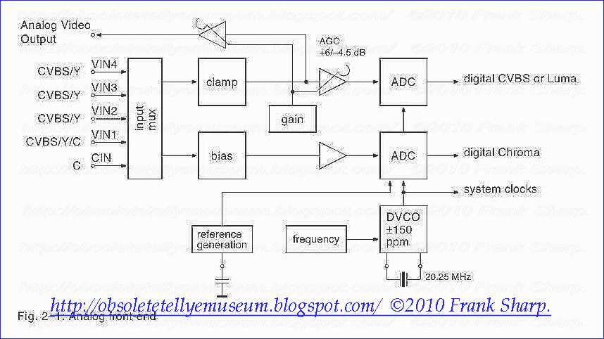
Fig. 1–2 depicts several VPC applications. Since the VPC functions as a video front-end, it must be comple- mented with additional functionality to form a complete TV set. The DDP 33x0 contains the video back-end with video postprocessing (contrast, peaking, DTI,...), H/V-deflection, RGB insertion (SCART, Text, PIP,...) and tube control (cutoff, white drive, beam current limiter). It generates a beam scan velocity modulation output from the digital YCrCb and RGB signals. Note that this signal is not generated from the external analog RGB inputs. The component interface of the VPC 32xxD provides a high-quality analog RGB interface with character insertion capability. It also allows appropriate processing of external sources, such as MPEG2 set-top boxes in transparent (4:2:2) quality. Furthermore, it transforms RGB/Fast Blank signals to the common digital video bus and makes those signals available for 100-Hz upconversion or double-scan processing. In some Euro- pean countries (Italy), this feature is mandatory. The IP indicates memory based image processing, such as scan rate conversion, vertical processing (Zoom), or PAL+ reconstruction. The VPC supports memory based applications through line-locked clocks, syncs and data. Additionally, the VPC323xD provides a 656-output interface and FIFO control signals.
Examples:
– Europe: 15 kHz/50 Hz → 32 kHz/100 Hz interlaced
– US: 15 kHz/60 Hz → 32 kHz/60 Hz non-interlaced
Fig. 1–2: VPC 32xxD applications
a) 15 kHz application Europe
b) double scan application (US, Japan) with YCrCb inputs
c) 100 Hz application (Europe) with RGBFB inputs
2. Functional Description
2.1. Analog Video Front-End
This block provides the analog interfaces to all video inputs and mainly carries out analog-to-digital conver- sion for the following digital video processing. A block diagram is given in Fig. 2–1. Most of the functional blocks in the front-end are digi- tally controlled (clamping, AGC, and clock-DCO). The control loops are closed by the Fast Processor (‘FP’) embedded in the decoder.

2.1.1. Input Selector
Up to five analog inputs can be connected. Four inputs are for composite video or S-VHS luma signal. These inputs are clamped to the sync back porch and are ampli- fied by a variable gain amplifier. One input is for connec- tion of S-VHS carrier-chrominance signal. This input is internally biased and has a fixed gain amplifier. A second S-VHS chroma signal can be connected video-input VIN1.
2.1.2. Clamping
The composite video input signals are AC coupled to the IC. The clamping voltage is stored on the coupling capacitors and is generated by digitally controlled cur- rent sources. The clamping level is the back porch of the video signal. S-VHS chroma is also AC coupled. The input pin is internally biased to the center of the ADC input range.
2.1.3. Automatic Gain Control
A digitally working automatic gain control adjusts the magnitude of the selected baseband by +6/–4.5 dB in 64 logarithmic steps to the optimal range of the ADC. The gain of the video input stage including the ADC is 213 steps/V with the AGC set to 0 dB.
2.1.4. Analog-to-Digital Converters
Two ADCs are provided to digitize the input signals. Each converter runs with 20.25 MHz and has 8 bit res- olution. An integrated bandgap circuit generates the required reference voltages for the converters. The two ADCs are of a 2-stage subranging type.
2.1.5. Digitally Controlled Clock Oscillator
The clock generation is also a part of the analog front end. The crystal oscillator is controlled digitally by the control processor; the clock frequency can be adjusted within ±150 ppm.
2.1.6. Analog Video Output
The input signal of the Luma ADC is available at the analog video output pin. The signal at this pin must be buffered by a source follower. The output voltage is 2 V, thus the signal can be used to drive a 75 Ω line. The magnitude is adjusted with an AGC in 8 steps together with the main AGC.
2.2. Adaptive Comb Filter
The 4H adaptive comb filter is used for high-quality luminance/chrominance separation for PAL or NTSC composite video signals. The comb filter improves the luminance resolution (bandwidth) and reduces interferences like cross-luminance and cross-color. The adap- tive algorithm eliminates most of the mentioned errors without introducing new artifacts or noise. A block diagram of the comb filter is shown in Fig. 2–2. The filter uses four line delays to process the informa- tion of three video lines. To have a fixed phase relation- ship of the color subcarrier in the three channels, the system clock (20.25 MHz) is fractionally locked to the color subcarrier. This allows the processing of all color standards and substandards using a single crystal fre- quency. The CVBS signal in the three channels is filtered at the subcarrier frequency by a set of bandpass/notch filters. The output of the three channels is used by the adaption logic to select the weighting that is used to reconstruct the luminance/chrominance signal from the 4 bandpass/notch filter signals. By using soft mixing of the 4 signals switching artifacts of the adaption algorithm are completely suppressed. The comb filter uses the middle line as reference, therefore, the comb filter delay is two lines. If the comb filter is switched off, the delay lines are used to pass the luma/chroma signals from the A/D converters to the luma/chroma outputs. Thus, the processing delay is always two lines. In order to obtain the best-suited picture quality, the user has the possibility to influence the behaviour of the adaption algorithm going from moderate combing to strong combing. Therefore, the following three parameters may be adjusted: – HDG ( horizontal difference gain ) – VDG ( vertical difference gain ) – DDR ( diagonal dot reducer ) HDG typically defines the comb strength on horizontal edges. It determines the amount of the remaining cross-luminance and the sharpness on edges respec- tively. As HDG increases, the comb strength, e. g. cross luminance reduction and sharpness, increases. VDG typically determines the comb filter behaviour on vertical edges. As VDG increases, the comb strength, e. g. the amount of hanging dots, decreases. After selecting the combfilter performance in horizontal and vertical direction, the diagonal picture perfor- mance may further be optimized by adjusting DDR. As DDR increases, the dot crawl on diagonal colored edges is reduced. To enhance the vertical resolution of the picture, the VPC provides a vertical peaking circuitry. The filter gain is adjustable between 0 – +6 dB and a coring filter suppresses small amplitudes to reduce noise artifacts. In relation to the comb filter, this vertical peaking widely contributes to an optimal two-dimensional resolution homogeneity.
2.3. Color Decoder
In this block, the standard luma/chroma separation and multi-standard color demodulation is carried out. The color demodulation uses an asynchronous clock, thus allowing a unified architecture for all color standards. A block diagram of the color decoder is shown in Fig. 2–4. The luma as well as the chroma processing, is shown here. The color decoder also provides several special modes, e.g. wide band chroma format which is intended for S-VHS wide bandwidth chroma. Also, filter settings are available for processing a PAL+ helper signal. If the adaptive comb filter is used for luma chroma separation, the color decoder uses the S-VHS mode processing. The output of the color decoder is YCrCb in a 4:2:2 format.
2.3.1. IF-Compensation
With off-air or mistuned reception, any attenuation at higher frequencies or asymmetry around the color subcarrier is compensated. Four different settings of the IF-compensation are possible (see Fig. 2–3): – flat (no compensation) – 6 dB/octave – 12 dB/octave – 10 dB/MHz The last setting gives a very large boost to high frequencies. It is provided for SECAM signals that are decoded using a SAW filter specified originally for the PAL standard.
2.3.2. Demodulator
The entire signal (which might still contain luma) is quadrature-mixed to the baseband. The mixing frequency is equal to the subcarrier for PAL and NTSC, thus achieving the chroma demodulation. For SECAM, the mixing frequency is 4.286 MHz giving the quadra- ture baseband components of the FM modulated chroma. After the mixer, a lowpass filter selects the chroma components; a downsampling stage converts the color difference signals to a multiplexed half rate data stream. The subcarrier frequency in the demodulator is generated by direct digital synthesis; therefore, substan- dards such as PAL 3.58 or NTSC 4.43 can also be demodulated.
ITT/MICRONAS SDA6000 Teletext Decoder with Embedded 16-bit Controller:Preface
M2 is a 16-bit controller based on Infineon’s C16x core with embedded teletext and
graphic controller functions. M2 can be used for a wide range of TV and OSD
applications. This document provides complete reference information on the hardware
of M2.
M2 is designed to provide absolute top performance for a wide spectrum of teletext and graphic applications in standard and high end TV-sets and VCRs. M2 contains a data caption unit, a display unit and a high performance Infineon C16x based microcontroller (so that M2 becomes a one chip TV-controller) an up to level 3.5 teletext decoder and display processor with enhanced graphic accelerator capabilities. It is not only optimized for teletext usage but also, due to its extremely efficient architecture, can be used as a universal graphic engine. M2 is able to support a wide range of standards like PAL, NTSC or applications like Teletext, VPS, WSS, Chinatext, Closed Caption and EPG (Electronic Program Guide). With the support of a huge number of variable character sets and graphic capabilities a wide range of OSD applications are also open for M2. A new flexible data caption system enables M2 to slice most data, making the IC an universal data decoder. The digital slicer concept contains measurement circuitries that help identify bad signal conditions and therefore support the automatic compensation of the most common signal disturbances. M2’s enhanced data caption control logic allows individual programming, which means that every line can carry an individual service to be sliced and stored in the memory. The display generation of M2 is based on frame buffer technology. A frame buffer concept displays information which is individually stored for each pixel, allowing greater flexibility with screen menus. Proportional fonts, asian characters and even HTML browsers are just some examples of applications that can now be supported. Thus, with the M2, the process of generation and display of on-screen graphics is split up into two independent tasks. The generation of the image in the frame buffer is supported by a hardware graphics accelerator which frees the CPU from power intensive address calculations. The graphics accelerator ‘prints’ the characters, at the desired ‘screen’ position, into the frame buffer memory based on a display list provided by the software. The second part of the display generator (the screen refresh unit) then reads the frame buffer according to the programmed display mode and screen refresh rate and converts the pixel information into an analog RGB signal. Furthermore, M2 has implemented an RGB-DAC for a maximum color resolution of state-of-the-art up to 65536 colors, so that the complete graphic functionality is implemented as a system on chip. The screen resolution is programmable up to SVGA, to cover today’s and tomorrow’s applications, only limited by the available memory (64 Mbit) and the maximum pixel clock frequency (50 MHz). The memory architecture is based on the concept of a unified memory - placing program code, variables, application data, bitmaps and data captured from the analog TV signal’s vertical blanking interval (VBI) in the same physical memory. M2’s external bus interface supports SDRAMs as well as ROMs or FLASH ROMs. The organization of the memory is linear, so that it is easy to program the chip for graphic purposes. The SW development environment “MATE” is available to simplify and speed up the development of the software and displayed information. MATE stands for: M2 Advanced Tool Environment. Using MATE, two primary goals are achieved: shorter Time-to-Market and improved SW qualitiy. In detail:
•
Re-usability
•
Target independent development
•
Verification and validation before targeting
•
General test concept
•
•
Graphical interface design for non-programmers
•
Modular and open tool chain, configurable by customer
MATE uses available C166 microcontroller family standard tools as well as a
dedicated M2 tools.
1.1
Features
General
••••••••••••••
Level 1.5, 2.5, 3.5 WST Display Compatible Fast External Bus Interface for SDRAM (Up to 8 MByte) and ROM or Flash-ROM (Up to 4 MByte) Embedded General Purpose 16 Bit CPU (Also used as TV-System Controller, C16x Compatible) Display Generation Based on Pixel Memory Program Code also Executable From External SDRAM Embedded Refresh Controller for External SDRAM Enhanced Programmable Low Power Modes Single 6 MHz Crystal Oscillator Multinorm H/V-Display Synchronization in Master or Slave Mode Free Programmable Pixel Clock from 10 MHz to 50 MHz Pixel Clock Independent from CPU Clock 3 ⌠ 6 Bits RGB-DACs On-Chip Supply Voltage 2.5 and 3.3 V P-MQFP-128 Package Microcontroller Features
•
16-bit C166-CPU Kernel (C16x Compatible)
•
60 ns Instruction Cycle Time
•
2 KBytes Dual Ported IRAM
•
2 KBytes XRAM On-chip
•
General Purpose Timer Units (GPT1 and GPT2).
•
Asynchronous/Synchronous Serial Interface (ASC0) with IrDA Support. Full-duplex
Asynchronous Up To 2 MBaud or Half-duplex Synchronous up to 4.1 MBaud.
•••••••••High-speed Synchronous Serial Interface (SSC). Full- and Half-duplex synchronous
up to 16.5 Mbaud
3 Independent, HW-supported Multi Master/Slave I2C Channels at 400 Kbit/s
16-Bit Watchdog Timer (WDT)
Real Time Clock (RTC)
On Chip Debug Support (OCDS)
4-Channel 8-bit A/D Converter
42 Multiple Purpose Ports
8 External Interrupts
33 Interrupt Nodes
Display Features•
•
OSD size from 0 to 2046 (0 to 1023) pixels in horizontal (vertical) direction
Frame Buffer Based Display
2 HW Display Layers
Support of Double Page Level 2.5 TTX in 100 Hz Systems
Support of Transparency for both Layers Pixel by Pixel
User Programmable Pixel Frequency from 10.0 MHz to 50 MHz
Up to 65536 Displayable Colors in one Frame
DMA Functionality
Graphic Accelerator Functions (Draw Lines, Draw and Fill Rectangle, etc.)
1, 2, 4 or 8-bit Bitmaps (up to 256 out of 4096 colors)
12 bit/16 bit RGB Mode for Display of up to 65535 Colors
HW-support for Proportional Characters
HW-support for Italic Characters
User Definable Character Fonts
Fast Blanking and Contrast Reduction Output
Acquisition Features
••
Two Independent Data Slicers (One Multistandard Slicer + one WSS-only Slicer)
Parallel Multi-norm Slicing (TTX, VPS, WSS, CC, G+)
Four Different Framing Codes Available
Data Caption only Limited by available Memory
Programmable VBI-buffer
Full Channel Data Slicing Supported
Fully Digital Signal Processing
Noise Measurement and Controlled Noise Compensation
Attenuation Measurement and Compensation
Group Delay Measurement and Compensation
Exact Decoding of Echo Disturbed Signals
Architectural Overview
The architecture of M2 comprises of a 16-bit microcontroller which is derived from the well known Infineon Technologies C16x controller family. Due to the core philosophy of M2, the architecture of the CPU core is the same as described in other Infineon Technologies C16x derivatives. The CPU, with its peripherals, can be used on one hand to perform all TV controlling tasks, and on the other hand to process the data, sliced by the slicer, and the acquisition unit according to the TTX standard. Furthermore it is used to gen
erate an “instruction list” for the graphic accelerator which supports the CPU by generating the display. M2 has integrated two digital slicers for two independent CVBS signals. One slicer is used to capture the data (e.g. Teletext or EPG) from the main channel, the other slicer can be used to slice the WSS information from a different channel, which is helpful e.g. to support PIP applications in 16:9 TVs. Both slicers separate the data from the analog signal and perform the bit synchronization and framing code selection before the data is stored in a programmable VBI buffer in the external RAM. Capturing and storing the raw data in the RAM does not need any CPU power. M2’s display concept has improved in comparison to the common known state of the art Teletext-ICs. The display concept is based on a pixel orientated attribute definition instead of the former character orientated attribute definition. For the processing of this new pixel based attribute definition the display generator architecture is divided in two subblocks: the graphic accelerator (GA) and the screen refresh unit (SRU). The graphic accelerator is used to modify the frame buffer. From an abstract point of view, the graphic accelerator is a DMA which is optimized for OSD functionality, so e.g. bitmaps can be copied to the frame buffer. The graphic accelerator is used to draw rectangles, parallelograms, horizontal, vertical and diagonal lines. The user does not need to access the graphic accelerator directly, thanks to an easy to handle SW-GDI function which is available with the M2 hardware. The DMA functionality of the display generator (DG) supports the pixel transfer between any address of entire external memory. The teletext and graphic capabilities can be used simultaneously, so that M2 can combine teletext information with e.g. background images and advanced high resolution OSD graphics. M2 uses the frame buffer located in external memory so every bitmap can be placed at any location on the screen. The contents of the frame buffer does not have to be set up in real time. The duration of the set up of the screen depends on the contents of the displayed information. M2 supports two hardware display layers. To refresh the screen the M2 reads and mixes two independent pixel sources simultaneously. Different formats of the pixels which are part of different applications (e.g. Teletext formats, 12-bit RGB or 16-bit RGB values) can be stored in the same frame buffer at the same time.Architectural Overview
The screen refresh unit is used to read the frame buffer pixel by pixel in real time and to
process the transparency and RGB data. A color look up table (CLUT) can be used to
get the RGB data of the current pixel. Afterwards the RGB data is transferred to the D/A
converter. The blank signal and contrast reduction signal (COR) is also processed for
each pixel by the SRU and transferred to the corresponding output pins.
The pixel, line and field frequencies are widely programmable so that the sync system
can be used from low end 50 Hz to high end 100 HZ TV applications as well as for any
other standard.
The on chip clock system provides the M2 with its basic clock signals. Independent
clock domains are provided for the embedded controller, the bus interface and the
display system. The pixel clock can vary between 10 MHz and 50 MHz.
Due to the unified memory architecture of M2, a new bus concept is implemented. An
arbiter handles the bus requests from the different request sources. These are:
•
Slicer 1 requests (normally used as a TTX slicer)
•
Slicer 2 requests (used as a WSS slicer)
•
Graphic accelerator requests
•
Screen refresh unit requests
•
Data requests from the CPU via XBUS
•
Instruction requests via the CPU program bus
For exploiting the full computational power of the controller core the code of time critical routines can be stored in one bank of the external SDRAM separated from all display information (frame buffer, character set etc.). An instruction cache (I-CACHE) is used for buffering instruction words in order to minimize the probability of wait states to occur when the microcontroller is interfering with the display generator (DG) for access rights to the external memory devices. The data cache (D-CACHE) serves for operand reads and writes via the XBUS from/to external memory devices. The external bus interface (EBI) features interleaved access cycles to one or two static external memory devices (ROM, Flash-ROM or SRAM) with a total maximum size of 4 MByte and one PC100 compliant (Intel standard) SDRAM device (16 MBit organized as 2 memory banks or 64 MBit organized as 4 memory banks). For TV controlling tasks M2 provides three serial interfaces (I2 C, ASC, SSC), two general purpose timers, (GPT1, GPT2), a real time clock (RTC), a watch dog timer (WDT), an A/ D converter and eight external interrupts.
M2’s microcontroller and its peripherals are based on a Cell-Based Core (CBC) which i
s compatible to the well known C166 architecture. In M2, the CPU and its peripherals are generally clocked with 33.33 MHz which results in an instruction cycle time of 60 ns. The implementation of the microcontroller within M2 deviates from other known C16x derivates since the controller’s XBUS is not used as the external bus. All external access cycles of the microcontroller, the display generator and the acquisition unit are performed via a high performance time interlocking SDRAM bus. The external bus interface (EBI) manages the arbitration procedure for access cycles to the external synchronous DRAM in parallel to an external static memory (ROM or FLASH; for more details refer to Chapter 4.4). Due to the realtime critical bus bandwidth requirements of the display generator, unpredictable wait-states for the controller may occur. These wait-states do not destroy the overall average system performance, because they are mostly buffered by the CPU related instruction and data buffers. Nevertheless they can influence, for example, the worst disconnection response time. Emulation is now performed by an on-chip debug module which can be accessed by a JTAG interface.The following microcontroller peripherals are implemented:
•
2 KByte IRAM (System RAM)
•
2 KByte XRAM (XBUS located)
•
32 Interrupt Nodes
•
General Purpose Timer Units (GPT1 and GPT2)
•
Real Time Clock (RTC)
•
Asynchronous/Synchronous Serial Interface (ASC0)
•
High-Speed Synchronous Serial Interface (SSC)
•
I2C Bus Interface (I2C)
•
4-Channel 8-bit A/D Converter (ADC)
•
Watchdog Timer (WDT)
•
On-Chip Debug Support Module (OCDS)
•
42 Multiple Purpose Ports
Central Processing Unit
The CPU executes the C166 instruction set (with the extensions of the C167 products).
Its main features are the following:
•
4-stage pipeline (Fetch, Decode, Execute and Write-Back).
•
16 ⌠ 16-bit General Purpose Registers
•
16-bit Arithmetic and Logic Unit
•
Barrel shifter
•
Bit processing capability
• Hardware support for multiply and divide instructions
Internal RAM (IRAM)
The internal dual-port RAM is the physical support for the General Purpose Registers, the system stack and the PEC pointers. Due to its close connections with the CPU, the internal RAM provides fast access to these resources. As the GPR bank can be mapped anywhere in the internal RAM through a base pointer (Context Pointer CP), fast context switching is allowed. The internal RAM is mapped in the memory space of the CPU and can be used also to store user variables or code. Interrupt Controller Up to 32 interrupt sources can be managed by the Interrupt Controller through a multiple priority system which provides the user with the ability to customize the interrupt handling. The interrupt system of M2 includes a Peripheral Event Controller (PEC). This processor performs single-cycle interrupt-driven byte or word transfers between any two locations in the entire memory space of M2. In M2, the PEC functionalities are extended by the External PEC which allows an external device to trigger a PEC transfer while providing the source and destination pointers. New features also include the packet transfer mode and the channel link mode. Besides user interrupts, the Interrupt Controller provides mechanisms to process exceptions or error conditions, so-called “hardware traps”, that arise during program execution.
System Control Unit
M2’s System Control Unit (CSCU) is used to control system specific tasks such as reset control or power management within an on-chip system built around the core. The power management features of the CSCU provide effective means to realize standby conditions for the system with an optimum balance between power reduction, peripheral operation and system functionality. The CSCU also provides an interface to the Clock Generation Unit (CGU) and is able to control the operation of the Real Time Clock (RTC).
The CSCU includes the following functions:
•
System configuration control
•
Reset sequence control
•
External interrupt and frequency output control
•
Watchdog timer module
•
General XBUS peripherals control
•
Power management additional to the standard Idle and Power Down modes
•
Control interface for Clock Generation Unit
•
Identification register block for chip and CSCU identification
OCDS
The On-Chip Debug System allows the detection of specific events during user program execution through software and hardware breakpoints. An additional communication module allows communication between the OCDS and an external debugger, through a standard JTAG port. This communication is performed in parallel to program execution.
Memory Organization
In normal operation mode the memory space of the CPU is configured in a “Von Neumann” architecture. This means that code and data are accessed within the same memory areas, i. e. external memory, internal controller memory (IRAM), the address areas for integrated XBUS peripherals (I 2C, internal XBUS memory (XRAM)) and the special function register areas (SFR, ESFR) are mapped into one common address space of 16 MBytes. This address space is arranged as 256 segments of 64 KBytes each and each segment is again subdivided into four data pages of 16 KBytes each. All internal memory areas and the address space of the integrated XBUS peripherals are mapped to segment 0. Code and data may be stored in any part of the memory, except for the SFR blocks, which can not be used for instructions. Despite this equivalence of code and data, proper partitioning is necessary to make use of the full bandwidth of the memory system. The integrated C16x controller communicates via 2 busses with the memory interface. In normal operation mode access to segments 00H to 41H (excluding internal memory areas) is mapped to the read only program memory bus (PMBUS), whereas access to segments 42H to FF H is mapped to the XBUS. In bootstrap loader mode (BSLMode) instruction fetches to external memory areas via PMBUS are redirected to the internal bootstrap loader ROM (BSLROM). Operand (data) accesses remain unchanged.
7.5
I2C-Bus Interface
The on-chip I2C Bus module connects the M2 to other external controllers and/or
peripherals via the two-line serial I2C interface. The I2C Bus module provides
communication at data rates of up to 400 Kbit/s and features 7-bit as well as 10-bit
addressing.
The module can operate in three different modes:
Master mode, where the I2C controls the bus transactions and provides the clock signal.
Slave mode, where an external master controls the bus transactions and provides the
clock signal.
Multimaster mode, where several masters can be connected to the bus, i.e. the I2C can
be master or slave.
The on-chip I 2C bus module allows efficient communication via the common I2C bus. The
module unloads the CPU of low level tasks such as
•
(De)Serialization of bus data.
•
Generation of start and stop conditions.
•
Monitoring the bus lines in slave mode.
•
Evaluation of the device address in slave mode.
•
Bus access arbitration in multimaster mode.
Features
•
Extended buffer allows up to 4 send/receive data bytes to be stored. Support of standard 100 KBaud and extended 400 KBaud data rates. Operation in 7-bit or 10-bit addressing mode. Flexible control via interrupt service routines or by polling. 7.5.1
Operational Overview
Data is transferred by the 2-line I2C bus (SDA, SCL) using a protocol that ensures reliable and efficient transfers. This protocol clearly distinguishes regular data transfers from defined control signals which control the data transfers. The following bus conditions are defined: Bus Idle: SDA and SCL remain high. The I2C bus is currently not used. Data Valid: SDA stable during the high phase of SCL. SDA then represents the transferred bit. There is one clock pulse for each transferred bit of data. During data transfers SDA may only change while SCL is low (see below)! Start Transfer: A falling edge on SDA ( ) while SCL is high indicates a start condition. This start condition initiates a data transfer over the I2C bus. Stop Transfer: A rising edge on SDA ( ) while SCL is high indicates a stop condition. This stop condition terminates a data transfer. An arbitrary number of bytes may be transferred between a start condition and a stop condition.
This mechanism allows a number of configurations of the physical I2C Bus interface:
Physical Channels
Can be selected, so the I2C module can use electrically separated channels or increase the addressing range by using more data lines. Note: Baud rate and physical channels should never be changed (via ICCFG) during a transfer.
Channel Switching
The I2 C module can be connected to a specific pair of pins (e.g. SDA0 and SCL0) which then forms a separate I2C channel to the external system. The channel can be dynamically switched by connecting the module to another pair of pins (e.g. SDA1 and SCL1). This establishes physically separate interface channels.
Broadcasting:
Connecting the module to more than one pair of pins (e.g. SDA0/1 and SCL0/1) allows the transmission of messages over multiple physical channels at the same time. Please note that this configuration is critical when the M2 is a slave. In master mode it cannot be guaranteed that all selected slaves have reached the message. Register ICCFG selects the bus baud rate as well the activation of SDA and SCL lines. So an external I2C channel can be established (baud rate and physical lines) with one single register access.
Operation in Master Mode
If the on-chip I2C module controls the I2C bus (i.e. bus master), master mode must be selected via bit field MOD in register ICCON. The physical channel is configured by a control word written to register ICCFG, defining the active interface pins and the used baud rate. More than one SDA and/or SCL line may be active at a time. The address of the remote slave that is to be accessed is written to ICRTB0 ... 3. The bus is claimed by setting bit BUM in register ICCON. This generates a start condition on the bus and automatically starts the transmission of the address in ICRTB0. Bit TRX in register ICCON defines the transfer direction (TRX = ‘1’, i.e. transmit, for the slave address). A repeated start condition is generated by setting bit RSC in register ICCON, which automatically starts the transmission of the address previously written to ICRTB0. This may be used to change the transfer direction. RSC is cleared automatically after the repeated start condition has been generated. The bus is released by clearing bit BUM in register ICCON. This generates a stop condition on the bus. Note: Between load the address in ICRTB0 an setting bit BUM at least one command (nop) has to be executed.
Operation in Multimaster Mode
If multimaster mode is selected via bit field MOD in register ICCON, the on-chip I 2C module can operate concurrently as a bus master or as a slave. The descriptions of these modes apply accordingly. Multimaster mode implies that several masters are connected to the same bus. As more than one master may try to claim the bus at a given time, an arbitration is done on the SDA line. When a master device detects a mismatch between the data bit to be sent and the actual level on the SDA (bus) line, it looses the arbitration and automatically switches to slave mode (leaving the other device as the remaining master). This loss of arbitration is indicated by bit AL in register ICST which must be checked by the driver software when operating in multimaster mode. Lost arbitration is also indicated when the software tries to claim the bus (by setting bit BUM) while the I2C bus is active (indicated by bit BB = ‘1’). Bit AL must be cleared via software.
Operation in Slave Mode
If the on-chip I2 C module is controlled via the I2C bus by a remote master (i.e. be a bus slave), slave mode must be selected via bit field MOD in register ICCON. The physical channel is configured by a control word written to register ICCFG
, defining the active interface pins and the used baud rate. It is recommended to have only one SDA and SCL line active at a time when operating in slave mode. The address by which the slave module can be selected is written to register ICADR. The I2C module is selected by another master when it receives (after a start condition), either its own device address (stored in ICADR) or the general call address (00 H). In this case an interrupt is generated and bit SLA in register ICST is set, indicating the valid selection. The desired transfer mode is then selected via bit TRX (TRX = ‘0’ for reception, TRX = ‘1’ for transmission). For a transmission the respective data byte is placed into the buffer ICRTB0 ... 3 (which automatically sets bit TRX) and the acknowledge behavior is selected via bit ACKDIS. For a reception the respective data byte is fetched from the buffer ICRTB0 ... 3 after IRQD has been activated. In both cases the data transfer itself is enabled by clearing bits IRQD, IRQP and IRQE which releases the SCL line. When a stop condition is detected, bit SLA is cleared. The I2 C bus configuration register ICCFG selects the bus baud rate (partly) as well as the activation of SDA and SCL lines. So an external I2C channel can be established (baud rate and physical lines) with one single register access. Systems that utilize several I2C channels can prepare a set of control words which configure the respective channels. By writing one of these control words to ICCFG the respective channel is selected. Different channels may use different baud rates. Also different operating modes can be selected, e.g. enabling all physical interfaces for a broadcast transmission.PHILIPS SAA4979H Sample rate converter with embedded high quality dynamic noise reduction and expansion portThe SAA4979H provides an economic stand-alone solution for 4 : 2 : 2 field rate upconversion (50 to 100 Hz or 60 to 120 Hz) including the required field memory combined with picture improvement features and dynamic field based noise reduction. The IC contains two digital input channels to allow field or frame based picture-in-picture processing. It also offers a feature expansion port for vector based motion estimation and compensation ICs such as SAA4991WP or SAA4992H.
FEATURES
• Digital YUV input according to ITU 656 standard
• 4 : 2 : 2 field rate upconversion (50 to 100 Hz or
60 to 120 Hz)
• 3.5-Mbit embedded DRAM
• Sample rate conversion for linear zoom and
compression
• Panorama mode
• Dynamic noise reduction
• Noise estimator
• Black bar detection
• Luminance horizontal smart peaking
• Digital Colour Transient Improvement (DCTI)
• Triple 10-bit Digital-to-Analog Converter (DAC)
• Line-locked PLL
• Expansion port for SAA4992H and SAA4991WP
• Double window and Picture-In-Picture (PIP) processing
• Embedded 80C51 microcontroller
• 32-Kbyte internal ROM (mask programmable)
• 512-byte internal RAM
FUNCTIONAL DESCRIPTION
Digital processing at 1fH level
ITU 656 DECODER
The SAA4979H provides 2 digital video input channels, which comply to the ITU 656 standard. 720 active video pixels per line are processed at a line-locked clock of 27 MHz, which has to be provided by the signal source. Luminance and chrominance information have to be multiplexed in the following order:
CB1, Y1, CR1, Y2, ... Timing reference codes must be
inserted at the beginning and end of each video line
(see Table 1):
• A ‘Start of Active Video’ (SAV) code before the first

active video sample (see Table 2)
• A ‘End of Active Video’ (EAV) code after the last active video sample (see Table 2). The incoming active video data must be limited to 1 to 254, since the data words 00H and FFH are used for identification of the timing reference headers. The digital signal input levels should comply to the CCIR-601 standard (see Fig.3). The data stream is decoded into the internal 4 : 2 : 2 YUV format at a 13.5 MHz clock rate. If required the sign of the UV signals can be inverted for both channels (control inputs: uv_sign1 and uv_sign2). The signal source of the main channel can be selected from both inputs by the internal microcontroller (control input: Select_data_input1).
7.1.2
DOUBLE WINDOW AND PICTURE-IN-PICTURE
PROCESSING
Data from the sub channel can be inserted into the data stream of the main channel by means of a fast switch. The two channels can be used together with one or two external field memories to implement, for example, double window or PIP processing. Both field based and frame based PIP processing is supported. The synchronization of the sub channel to the main channel is achieved by providing synchronized read signals (RE2 and RSTR2) for the external field memories, whereas the write signals need to be provided together with the incoming data by the external signal source. A multi-PIP mode is also supported by freezing the data in the internal field memory within certain areas via the programmable internal control signal IEint.
7.1.3
BLACK BAR DETECTOR Black bar detection searches for the last black line in the upper part of the screen and for the first black line in the lower part of the screen. The detection is done within a programmable window (control inputs: bbd_hstart, bbd_hstop, bbd_vstart and bbd_vstop). To avoid disturbances of LOGOs in the video, the window can be shifted to the horizontal centre of the lines. A video line is considered to be black if the luminance values of that line within the detection window are not greater than a certain slice level (control input: bbd_slice_level) for more than a specific number of pixels (control input: bbd_event_value). The numbers of the first and the last active video line can be read out by the microcontroller (control outputs: bbd_1st_videoline and bbd_last_videoline).
7.1.4
DYNAMIC NOISE REDUCTION
The main function of the noise reduction is shown in Fig.4. It is divided into two signal paths for chrominance and luminance. In principal two operating modes can be used, the fixed and the adaptive mode. In both modes the applied frequency range, in which the noise reduction takes place, can be reduced or not reduced (control input: unfiltered). The noise reduction operates field recursive with an averaging ratio (K factor) between fresh (new) and over previous fields averaged (old) luminance and chrominance values. Noise reduction can be activated by forcing the NREN control bit to HIGH. If NREN is LOW the noise reduction block is bridged via a data multiplexer. In the fixed mode, the noise reduction produces a constant weighted input averaging. Because of smearing effects this mode should not be used for normal operation except for K = 1. The fixed mode can be activated separately for chrominance (control input: chromafix) and luminance (control input: lumafix). In the adaptive mode, the averaging ratio is based on the absolute differences of the inputs of luminance and chrominance respectively. If the absolute difference is low, only a small part of the fresh data will be added. In cases of high difference, much of the fresh data will be taken. This occurs either in situations of movement or where a significant vertical contrast is seen. The relationship between the amount of movement and the K factor values is defined in a look-up table where the steps can be programmed (control input: Kstep). It should be noted that recursion is done over fields, and that pixel positions between the new and old fields always have a vertical offset of one line. So averaging is not only done in the dimension of time but also in the vertical direction. Therefore averaging vertically on, for example, a vertical black to white edge would produce a grey result. The averaging in chrominance can optionally be slaved to the luminance averaging (control input: Klumatochroma), in that case chrominance differences are not taken into account for the K factor setting of the chrominance signal path. The noise reduction scheme also decreases the cross-colour patterns effectively if the adaptive noise reduction for the averaging in chrominance is slaved to the luminance averaging (control input: Klumatochroma). The cross-colour pattern does not produce an increase of the measured luminance difference, therefore this pattern will be averaged over many fields.
7.1.4.1
Band-splitting
The frequencies of the difference signals of luminance
(delta Y) and chrominance (delta U/V) can be split
optionally into an upper band (HF) and a lower band (LF)
with a low-pass filter in both signal paths. The lower
frequency band signals (LF delta Y and LF delta U/V) are
used as input for the noise reduction function.
The lower frequency band of the difference signals can
also be used for the motion detection. If, for example, only
the lower frequency band contains information, the
specific picture content does not move or is moving slowly.
Optionally it is possible to bridge the band-splitting (control
input: unfiltered = 1).
7.1.4.2
Motion detection
The same signals (the noise reduction is applied to) are
also used to detect the amount of motion in the difference
signals. Therefore, the absolute values of the difference
signals are generated and limited to a maximum value.
The absolute values of the difference signal of U and V are
then averaged. The signals are low-pass filtered for
smoothing these signals. The filtered signals are amplified,
depending on the setting of the control inputs:
Yadapt_gain and Cadapt_gain respectively.
The amplified signals, which correlate to the amount of
movement in the chrominance or luminance signal path,
are transferred into 1 out of 9 possible K factor values via
look-up tables. The look-up tables consist of 9 intervals,
each related to one K factor. The boundaries between the
9 intervals are defined by 8 programmable steps (control
inputs: Kstep0 to Kstep7). The step values are valid for the
look-up tables for both the chrominance and the luminance
path. For example, signal values between Kstep2 and
Kstep3 result in a K factor of K = 3/8.
7.1.4.3
K factor
The amount of noise reduction (field averaging) is described my means of the K factor. When K = 1 no averaging is applied and the new field information is used. When K = 0 no averaging is applied and thus only the old field information is used like in a still picture mode. All values inbetween mean that a weighted averaging is applied. It is possible to use fixed K factor values if the control inputs lumafix or chromafix are set to logic 1. The possible fixed K factor values of the control inputs Klumafix and Kchromafix are given in Table 6.
7.1.4.4
Noise shape
Possible shadow picture information in the chrominance and luminance path, resulting from a low K factor value, will be eliminated if the noise shaping is activated. The noise shaping function can be switched off via the microcontroller (control input: noiseshape).
7.1.5
NOISE ESTIMATOR
The noise level of the luminance signal can be measured within a programmable window (control inputs: ne_hstart, ne_hstop, ne_vstart and ne_vstop). The correlation in flat areas is used to estimate the noise in the video signal. A large number of estimates of the noise is calculated for every video field. Such an estimate is obtained by summing absolute differences between current pixel values and delayed pixel values within blocks of 4 pixels. Within the lower part of the total range of possible estimates 15 intervals are defined. Each interval is defined by a lower boundary and an upper boundary. The lower boundary is equal to the number of the interval, whereas the upper boundary has a fixed relationship to the lower boundary (control input: gain_upbnd). The lower boundary is increased or decreased by 1 in each field until an interval is found which contains at least a predefined number of estimates, and is at the same time lowest in the range. The value of the lower boundary of this interval determines the current noise figure output. The predefined number of estimates can be set via the microcontroller (control input: wanted_value), and good results were obtained with a value which is approximately 0.27% of the total number of blocks. For video fields with a lot of noise the number of small differences is very low, that means the number of noise estimates in the lower intervals is close to 0. Contrary to this, for clean sequences this number is very high. This means that for clean sequences the noise estimate figure will be close to 0, and for sequences with a lot of noise the noise estimate figure (control output: nest) will reach 15. To improve the performance of the noise estimator, several functions are implemented which can be controlled by the microcontroller. To increase the sensitivity of the noise measurement a prefilter with different gain settings is available (control input: Ypscale). Since the video content, e.g. sequences with a lot of high frequencies, can influence the noise estimate figure, a detail-counter is built-in.
The detail-counter calculates the number of absolute differences between current and previous pixels within a programmable interval defined by the control inputs lb_detail and upb_detail. The result of the 16-bit detail-counter (control outputs: detail_cnt_h and detail_cnt_l) can be used to increase or decrease the result of the noise estimation figure (control input: compensate). In order to reduce the effect of clipping, only the blocks where the sum of the luminance value is within a predefined range are taken into account. The control signal clip_offs can be used to increase or decrease this range. A grey-counter gives information whether enough pixels with values in the grey range are present in a video field (control output: grey_cnt). When this number is lower than a predefined threshold, e.g. for complete fields towards black or white, all blocks are taken into account.
7.2
Embedded DRAM
7.2.1
3.5-MBIT FIELD MEMORY
The basic functionality of the field memory, which is shown in Fig.5, is similar to the SAA4956TJ. The memory size is extended to 3538944 bits. The data path is 16-bit wide (8-bit chrominance and 8-bit luminance). The field memory is capable of storing, for example, up to 307 video lines of 720 pixels in a 4 : 2 : 2 format. After writing or reading 18 words of 16-bit width, a data transfer is performed from the serial to parallel data registers (writing) or from the parallel to the serial registers (reading). The field memory has one write interface (controller and registers) to store 1fH data and two read interfaces, one to read field delayed 1fH data for the noise reduction function and the other to read 2fH data for the following data processing. Since two asynchronous clock domains are involved (SWCKint as 1fH clock and SRCKint as 2fH clock) the read and write access to the memory array is controlled asynchronously by the memory arbitration logic triggered via request and acknowledge pulses. The write operation starts with a reset write (RSTWint) address pointer operation during the write enable (WEint) LOW phase. The RSTWint LOW-to-HIGH transition, referred to the rising edge of the write clock SWCKint, must be at least 18 clock cycles ahead of the first written data (WEint HIGH) and 18 clock cycles after the last written data. The reset write transfers data temporarily stored in the serial write registers to the memory array and resets the write counter to the lowest address. Write enable (WEint) is used to enable or disable a data write operation. The WEint signal controls the data inputs D0 to D15. In addition, the internal write address pointer is incremented if WEint is HIGH at the positive transition of the SWCKint write clock. The data is latched if WEint was HIGH at the previous positive transition of SWCKint. Input enable (IEint) LOW can also suppress the storage of the data into the memory array but does not influence the write pointer increment. It is used to freeze parts of the field data e.g for PIP processing. The read operation starts with a reset (RSTRint) of the read address pointer during the read enable (REint) LOW phase. The RSTRint LOW-to-HIGH transition, referred to the rising edge of the read clock SRCKint, must be at least 18 clock cycles ahead of the first read data (REint HIGH) and 18 clock cycles after the last read data. The reset read resets the read counter to the lowest address and requests a read operation of the data of the lowest address to the serial read register. Read enable (REint) is used to enable or disable the read operation. The REint controls the data outputs Q0 to Q15. REint HIGH increments the read counter. In parallel to the write operation a read2 operation is done using the same control signals as the write operation: SWCKint, WEint and RSTWint. It reads the old data of the previous field. The data Qold is needed as data input (Dfielddelay) for the noise reduction. When the WEint signal is HIGH it indicates that active video (valid 1fH data) is to be stored. The start of WEint HIGH is triggered by the H and V status bits of the ITU data stream. The start of WEint HIGH can be delayed by the control signals weint_hstart (number of clock delays) and weint_vstart (number of video lines delay). The stop of WEint HIGH is controlled by weint_hstop and weint_vstop. When the IEint signal is HIGH it indicates that active video (valid 1fH data) is also to be stored. The video data is not stored and earlier written data is maintained (frozen) if WEint is HIGH and IEint is LOW. The start of IEint HIGH is triggered by the H and V status bits of the ITU data stream. The start of IEint HIGH can be delayed by the control signals ieint_hstart (number of clock delays) and ieint_vstart (number of video lines delay). The stop of IEint HIGH is controlled by ieint_hstop and ieint_vstop. RSTWint is triggered by the V status bit of the ITU data stream. RSTRint is identical to the VD output signal. REint is provided by the following sample rate conversion to gather 2fH data if it is needed.
7.3
Digital processing at 2fH level
7.3.1
SAMPLE RATE CONVERSION
The sample rate conversion block is used to obtain 848 active pixels per line out of the original 720 pixels according to the relation of the two sampling frequencies (32 MHz and 27 MHz). The interpolation for phase positions between the original samples is achieved with a variable phase delay filter with 10 taps for luminance signals and 6 taps for chrominance signals. The conversion to a higher sample frequency of 32 MHz is done to improve the motion estimation performance in combination with external feature ICs, which can process up to 848 pixels per line at a 32 MHz clock. Bypassing this function keeps the original 720 pixels per line (control input: bypass_FSRC).
7.3.2
EXPANSION PORT
For a further extension of the system an expansion port is available, which is applicable for either a 4 : 2 : 2 format or a reduced 4 : 1 : 1 format for data input and output at a 32 MHz line-locked clock; see Table 3. However, the internal data is processed in a 8-bit wide 4 : 2 : 2 format. To generate the 4 : 1 : 1 format at the output the U and V samples from the 4 : 2 : 2 data stream are filtered by a low-pass filter, before being subsampled with a factor of 2 and formatted to 4 : 1 : 1 format. Bypassing this function keeps the data in the 4 : 2 : 2 format. An internal bandwidth detector is implemented to detect whether the colour difference signals provide either the full 4 : 2 : 2 bandwidth or a reduced 4 : 1 : 1 bandwidth. Therefore absolute differences between original data and downsampled data are calculated and can be read out by the microcontroller (control output:
UV_bw_detect). Low absolute differences indicate that the original data does not contain the full 4 : 2 : 2 bandwidth. This information can be used to switch the upsample and downsample filter on or off (control inputs: bypass_upsampling and bypass_downsampling). Bandwidth detection is done within a programmable window (control inputs: bw_hstart, bw_hstop and bw_vstart, bw_vstop). In the event of a 4 : 1 : 1 format at the input an upconverter to 4 : 2 : 2 is applied with a linear interpolation filter for creation of the extra samples. These are combined with the original samples from the 4 : 1 : 1 stream. The first phase of the YUV data stream is available on the output bus two clock cycles after the rising edge of the REI input signal. The start position, when the first phase of the YUV data stream arrives on the input bus, can be set via the control register exp_hstart. The luminance output signal is in 8-bit straight binary format, whereas the chrominance output signals are in twos complement format. The input data at the expansion slot is expected in the same format. U and V input signals are inverted if the corresponding control bit mid_uv_inv isset.
7.3.3
PANORAMIC ZOOM
The panoramic zoom block contains a second sample rate
converter, which performs the following tasks:
• Linear horizontal sample rate conversion in both zoom
and compress direction, with a sample rate conversion
factor between 0 and 2, meaning infinite zoom up to a
compression with a factor of 2
• Dynamic sample rate conversion e.g. for panorama
mode display of 4 : 3 material on a 16 : 9 screen.
For linear horizontal zoom or compression the sample rate
conversion factor is static during a video line (control
input: c0). Positive values of c0 are suitable for
compression, negative values result in expansion.
In panorama mode the video lines are geometrically
expanded towards the sides. The sample rate conversion
factor is modulated along the video line. A parabolic shape
of the sample rate conversion factor can be obtained with
the parameter c2, which controls the second order
variation of the sample rate. Negative values of c2 are
suitable for panorama mode, positive values result in the
inverse mode (amaronap mode).
The panoramic zoom block also provides a dynamically
controlled delay with an accuracy up to 1⁄64 of a pixel and
a range of −0.5 to +0.5 lines (control input: hshift).
Sufficient accuracy in interpolation for phase positions
between the original samples is achieved with a variable
phase delay filter with 10 taps for luminance signals and
6 taps for chrominance signals.
7.3.4
DIGITAL COLOUR TRANSIENT IMPROVEMENT
The Digital Colour Transient Improvement (DCTI) is
intended for U and V signals originating from a 4 : 1 : 1
source. Horizontal transients are detected and enhanced
without overshoots by differentiating, make absolute and
again differentiating the U and V signals separately. This
results in a 4 : 4 : 4 U and V bandwidth. To prevent
third-harmonic distortion, which is typical for this
processing, a so called over the hill protection prevents
peak signals becoming distorted.
It is possible to control the following settings via the
microcontroller: gain width (see Fig.10), threshold (i.e.
immunity against noise), selection of simple or improved
first differentiating filter (see Fig.9), limit for pixel shift
range (see Fig.11), common or separate processing of
U and V signals, hill protection mode (i.e. no
discolourations in narrow colour gaps), low-pass filtering
for U and V signals (see Fig.12) and a so called super hill
mode, which avoids discolourations in transients within a
colour component.
7.3.5
HORIZONTAL SMART Y PEAKING
A linear peaking is applied, which amplifies the luminance signal in the middle and the upper ranges of the bandwidth. The filtering is an addition of: • The original signal • The original signal high-passed with maximum gain at a frequency of 1⁄2fs (sample frequency fs = 32 MHz) • The original signal band-passed with a centre frequency of 1⁄4fs • The original signal band-passed with a centre frequency of 4.76 MHz. The band-passed and high-passed signals are weighted with the factors 0, 1⁄16, 2⁄16, 3⁄16, 4⁄16, 5⁄16, 6⁄16 and 8⁄16, resulting in a maximum gain difference of 2 dB per step at the centre frequencies. Coring is added to avoid amplification of low amplitudes in the high-pass and band-pass filtered signals, which are considered to be noise. The coring threshold can be programmed as 0 (off), ±4, ±8, ±12 to ±60 LSB with respect to the (signed) 10-bit signal. In addition the peaking gain can be reduced depending on the signal amplitude, programming range 0 (no attenuation), 1⁄4, 2⁄4 and 4⁄4. It is also possible to make larger undershoots than overshoots, programming range 0 (no attenuation of undershoots), 1⁄4, 2⁄4 and 4⁄4. A steepness detector is built-in, which provides information for dynamic control of the peaking. For that the maximum absolute value of the band-pass filtered signal within a video field is calculated and can be read out by the microcontroller (control output: steepness_max).
7.3.6
NON-LINEAR PHASE FILTER
The non-linear phase filter adjusts possible group delay differences in the Y, U and V output channels. The filter coefficients are: [−λ × (1 − μ); 1 + λ; −λ × μ] where λ determines the strength of the filter and μ determines the asymmetry. The effect of the asymmetry is a decrease in the delay for higher frequencies with μ ≤ 0.5. Control settings are provided for λ = 0, 1⁄8, 2⁄8, 3⁄8 and μ = 0, 1⁄4, 1⁄2.
7.3.7
POST PROCESSING
Blanking is done just before the digital-to-analog conversion by switching Y to a fixed black value and UV to a colourless value. The blanking window is defined by the control inputs: bln_hstart, bln_hstop, bln_vstart and bln_vstop. Side panels are generated by switching the Y, U and V to defined values within a horizontal window (control inputs: sidepanel_hstart and sidepanel_hstop); the 8 MSBs of Y and the 4 MSBs of U and V are programmable (control inputs: sidepanel_y, sidepanel_u and sidepanel_v). Framing e.g. for picture-in-picture mode, can be achieved by another programmable window (control inputs: PIP_frame_hstart, PIP_frame_hstop, PIP_frame_vstart and PIP_frame_vstop). The vertical and horizontal frame width can be programmed from 1 up to 15 pixels (control inputs: PIP_frame_heigth and PIP_frame_width). Framing uses the same colour and luminance values as the side panels. The range of the Y output signal can be chosen between 9 and 10 bits (control input: output_range). In the event of 9 bits for the nominal signal there is room left for under and overshoot, adding up to a total of 10 bits. In the event of selecting all 10 bits of the luminance digital-to-analog converter for the nominal signal any under or overshoot will be clipped (see Fig.6). The Y samples can be shifted onto 16 positions with respect to the UV samples (control input: y_delay). The zero delay setting is suitable for the nominal case of aligned input data. The other settings provide eight samples with less delay to seven samples with more delay in Y.
7.4
Triple 10-bit digital-to-analog conversion Three identical 10-bit converters are used to map the 4 : 4 : 4 YUV data to analog levels with a 32 MHz data rate. The polarity of the colour difference signals U and V is switchable by the control bit uv_inv_out. The output ranges are illustrated in Figs 6 and 7 respectively.
7.5
Microcontroller
The SAA4979H contains an embedded 80C51 microcontroller core including 512-byte RAM and 32-Kbyte ROM. The microcontroller runs on a 16 MHz clock, generated by dividing the 32 MHz display clock by a factor of 2.
7.5.1
HOST INTERFACE
For controlling internal registers a host interface, consisting of a parallel address and data bus, is built-in. The interface can be addressed as internal AUXRAM via a MOVX type of instruction. The complete range of internal control registers and the corresponding host addresses are described in Section 8.1. User access to these control registers via the I2C-bus can be implemented in the embedded software.
7.5.2
I2C-BUS INTERFACE
The I2C-bus interface in the SAA4979H is used in a slave receive and transmit mode for communication with a central system microcontroller. The standardized bus frequencies of both 100 kHz and 400 kHz can be accommodated. The I2C-bus slave address of the SAA4979H is 0110100 R/W. During slave transmit mode the SCL LOW period may be extended by pulling SCL to LOW (in accordance with the I2C-bus specification). Detailed information about the software dependent I2C-bus subaddresses of the control registers and a detailed description of the transmission protocol can be found in Application Note “I2C-bus register specification of the SAA4979H”.
7.5.3
SNERT-BUS INTERFACE
A SNERT interface is built-in, which operates in a master receive and transmit mode for communication with peripheral circuits such as SAA4991WP or SAA4992H. The SNERT interface replaces the standard UART interface. Contrary to the 80C51 UART interface there are additional special function registers (see Table 10) and there is no byte separation time between address and data.
The SNERT interface transforms the parallel data from the microcontroller into 1 or 2 Mbaud SNERT data, switchable via microcontroller. The SNERT-bus consists of three signals: SNCL used as serial clock signal, generated by the SNERT interface; SNDA used as bidirectional data line and SNRST used as reset signal, generated by the microcontroller at port pin P1.0 to indicate the start of a transmission. The read or write operation must be set by the microcontroller. When writing to the bus, 2 bytes are loaded by the microcontroller: one for the address, the other for the data. When reading from the bus, one byte is loaded by the microcontroller
for the address, the received byte is the data from the addressed SNERT location.7.5.4
I/O PORTS
A parallel 8-bit I/O port (P1) is available, where P1.0 is used as SNERT reset signal (SNRST), P1.2 to P1.5 can be used for application specific control signals, and P1.6 and P1.7 are used as I2C-bus signals (SCL and SDA).
7.5.5
WATCHDOG TIMER
The microcontroller contains an internal Watchdog timer, which can be activated by setting the corresponding special function register PCON.4. Only a synchronous reset will clear this bit. To prevent a system reset the Watchdog timer must be reloaded within a specified time. The Watchdog timer contains an 11-bit prescaler and is therefore incremented every 0.768 ms (16 MHz clock). The time interval between the timers reloading and the occurrence of a reset depends on the reloaded 8-bit value.
7.5.6
RESET
A reset is accomplished by holding the RST pin HIGH for at least 0.75 μs while the display clock is running and the supply voltage is stabilized.
7.6
System controller
The system controller provides all necessary internal read and write signals for controlling the embedded field memory. The required control signals (REO and IE) for applications with motion compensation circuits and the drive signals (HD and VD) for the horizontal and vertical deflection power stages are also generated. The system controller also supports double window or picture-in-picture processing in combination with an external field memory by providing the required memory control signals (RE2, RSTW2 and OIE2). The system controller is connected to the microcontroller via the host interface.
7.6.1
READ ENABLE OUTPUT
The Read Enable Output (REO) signal is intended for control of an external feature IC. It is a composite signal consisting of a horizontal and a vertical part. The horizontal and vertical positions are programmable (control inputs: reo_hstart, reo_hstop, reo_vstart and reo_vstop).
7.6.2
READ ENABLE INPUT
The Read Enable Input (REI) signal is used in applications with external feature ICs connected to the expansion port. It has to be provided by the external circuit (see Section 7.3.2).
7.6.3
INPUT ENABLE
The Input Enable (IE) signal is intended for control of field memories in applications together with an external feature IC connected to the expansion port. It can be directly set or reset via the microcontroller.
7.6.4
HORIZONTAL DEFLECTION
The Horizontal Deflection (HD) signal is for driving a deflection circuit; start and stop values of the horizontal position are programmable in a resolution of 4 clock cycles (control inputs: hd_start and hd_stop).
7.6.5
VERTICAL DEFLECTION
The Vertical Deflection (VD) signal is for driving a deflection circuit. This signal has a cycle time of 10 ms and the start and stop values of the vertical position are programmable in steps of 16 μs (control inputs: vd_start and vd_stop).
7.6.6
AUXILIARY DISPLAY SIGNAL
The Auxiliary Display Signal (ADS) is for general purposes; the horizontal and vertical positions are programmable (control inputs: ads_hstart, ads_hstop, ads_vstart and ads_vstop). 7.6.7
READ ENABLE 2
The Read Enable 2 (RE2) signal is intended for control of an external field memory at input channel 2 in picture-in-picture applications. It is a composite signal consisting of a horizontal and a vertical part. The horizontal and vertical positions are programmable (control inputs: re2_hstart, re2_hstop, re2_vstart and re2_vstop).
7.6.8
OUTPUT/INPUT ENABLE 2
The Output/Input Enable 2 (OIE2) signal is intended for control of one or two external field memories at input channel 2 in picture-in-picture applications. It can be directly set or reset via the microcontroller.
7.6.9
RESET READ 2
The Reset Read 2 (RSTR2) signal is intended for control of the read access of an external field memory at input channel 2 in picture-in-picture applications. It is derived from the internal vertical reference signal of the main channel.
7.6.10
RESET WRITE 2
The Reset Write 2 (RSTW2) input is used in picture-in-picture applications with an external field memory at input channel 2, and has to be provided by an external circuit which controls the field memory write access.
7.7
Line-locked clock generation
An internal PLL generates the 32 MHz line-locked display clock CLK32. The PLL consists of a ring oscillator, DTO and digital control loop. The PLL characteristic is controlled by means of the microcontroller.
7.8
Boundary scan test
The SAA4979H has built-in logic and 6 dedicated pins to support boundary scan testing which allows board testing without special hardware (nails). The SAA4979H follows the “IEEE Std. 1149.1 - Standard Test Access Port and Boundary-Scan Architecture” set by the Joint Test Action Group (JTAG) chaired by Philips. The 6 special pins are Test Mode Select (TMS), Test Clock (TCK), Test Reset (TRST), Test Data Input (TDI), Boundary-scan Compliant Enable (BCE) and Test Data Output (TDO). To achieve compliance to the “IEEE Std. 1149.1” a logic HIGH has to be applied to the BCE pin. Internal pull-up resistors at the input pins TMS, TRST and TDI are not implemented.
The SAA4979H supports different scan-rate upconversion concepts. The simple one is illustrated in Fig.17
. In this application no further components are needed for a 100 Hz conversion based on a field repetition algorithm (AABB mode). The system can be upgraded by a vector based motion estimation and compensation function. In this case the SAA4992H together with two field memories (SAA4955) are needed (see Figs 18 and 19 respectively). In addition the SAA4979H supports field based and frame based picture-in-picture applications. To realize the full performance frame based PIP function a second video decoder (SAA7118) and two additional field memories are required.ITT/MICRONAS MSP3400C MSP3411 Multistandard, Sound Processor:
Multistandard Sound Processor
Release Notes: The hardware description in this
document is valid for the MSP 3400C – C8 and newercodes. Revision bars indicate significant changes
to the previous version.
1. Introduction
The MSP 3400C is designed as single-chip Multistandard
Sound Processor for applications in analog and
digital TV sets, satellite receivers and video recorders.
The MSP-family, which is based on the MSP 2400, demonstrates
the progressive development towards highly
integrated multi-functional ICs.
The MSP 3400C, again, improves function integration:
The full TV sound processing, starting with analog
sound IF signal-in, down to processed analog AF-out, is
performed in a single chip. The IC is produced in 0.8 mm
CMOS technology, combined with high performance
digital signal processing.
The MSP 3400C 0.8 m CMOS version is fully pin and
software compatible to the 1.0 m MSP 3400 and MSP
3410. The main difference between the MSP 3400C and
the MSP 3410, consists of the MSP 3410 being able to
decode NICAM signals.
The MSP 3400C is available in PLCC68, PSDIP64,
PSDIP52, and PQFP80 package.
Note: To achieve compatibility with the functions of MSP
3400 and MSP 3410 (except NICAM), the load sequences
must be programmed as described in the data
sheet of MSP 3410.
MSP 3400C Integrated Functions:
– FM-demodula
tion of all terrestrial standards (incl. identification decoding)
– FM-demodulation of all satellite standards
– various deemphasis types (incl. Panda1)
– volume, balance, bass, treble, loudness for loudspeaker and headphone output
– automatic volume correction (A.V.C.)
– 5 band graphic equalizer
– subwoofer output alternatively with headphone output
– spatial effect (pseudostereo/basewidth enlargement)
– ADR together with DRP 3510 A
– Dolby ProLogic together with DPL 3418/19/20 A
– 3 pairs of D/A converters
– 1 pair of A/D converters
– SCART switches
2. Features of the MSP 3400C
2.1. Features of the Demodulator and Decoder
Sections
The MSP 3400C is designed to perform demodulation
of FM-mono TV sound and two carrier FM systems according
to the German or Korean terrestrial specs. With
certain constraints, it is also possible to do AM-demodulation
according to the SECAM system. Alternatively, the
satellite specs can be processed with the MSP 3400C.
For FM carrier detection in satellite operation, the AMdemodulation
offers a powerful feature to calculate the
carrier field strength, which can be used for automatic
search algorithms. So, the IC facilitates a first step towards
multistandard capability with its very flexible
application and may be used in TV-sets, satellite tuners,
and video recorders.
The MSP 3400C facilitates profitable multistandard capability,
offering the following advantages:
– two selectable analog inputs (TV and SAT-IF sources)
– Automatic Gain Control (AGC) for analog input: input
range: 0.14 – 3 Vpp
– integrated A/D converter for sound-IF inputs
– all demodulation and filtering is performed on chip and
is individually programmable
– no external filter hardware is required
– only one crystal clock (18.432 MHz) is necessary
– FM carrier level calculation for automatic search algorithms
and carrier mute function
– high deviation FM-mono mode (max. deviation:
approx. 360 kHz)
2.2. Features of the DSP-Section
– flexible selection of audio sources to be processed
– digital input and output interfaces via I2S-Bus for external
DSP-processors, surround sound, ADR etc.
– digital interface to process ADR (Astra Digital Radio)
together with DRP 3510 A
– performance of all deemphasis systems including
adaptive Wegener Panda 1 without external components
or controlling
– digitally performed FM-identification decoding and dematrixing
– digital baseband processing: volume, bass, treble,
5-band equalizer, loudness, pseudostereo, and basewidth
enlargement
– simple controlling of volu
me, bass, treble, equalizeretc.
– increased audio bandwidth for FM-Audio-signals
(20 Hz – 15 kHz, 1 dB)
2.3. Features of the Analog Section
– three selectable analog pairs of audio baseband inputs
(= three SCART inputs)
input level: 32 V RMS,
input impedance: .25 kW
– one selectable analog mono input (i.e. AM sound),
input level: 32 V RMS,
input impedance: .10 kW
– two high quality A/D converters, S/N-Ratio: .85 dB
– 20 Hz to 20 kHz Bandwidth for SCART-to-SCARTCopy
facilities
– MAIN (loudspeaker) and AUX (headphones): two
pairs of 4-fold oversampled D/A-converters
output level per channel: max. 1.4 V RMS
output resistance: max. 5 kW
S/N-Ratio: .85 dB at maximum volume
max. noise voltage in mute mode: 310 mV (BW: 20 Hz
...16 kHz)
– one pair of four-fold oversampled D/A-converters supplying
two selectable pairs of SCART-Outputs. Output
level per channel: max. 2 V RMS, output resistance:
max. 0.5 kW, S/N-Ratio: .85 dB
(20 Hz...16 kHz)
3. Application Fields of the MSP 3400C
The MSP 3400C processes TV sound according to the
German and Korean two carrier system and the commonly
used satellite systems. In the following sections,
a brief overview on the German FM-Stereo system
shows what is required of a multistandard audio IC.
3.1. German 2-Carrier System (DUAL FM System)
Since September 1981, stereo and dual sound programs
have been transmitted in Germany using the
2-carrier system. Sound transmission consists of the already
existing first sound carrier and a second sound
carrier additionally containing an identification signal.
4. Architecture of the MSP 3400C
Fig. 4–1 shows a simplified block diagram of the IC. Its
architecture is split into three functional blocks:
1. demodulator section
2. digital signal processing (DSP) section performing
audio baseband processing
3. analog section containing two A/D-converters,
6 D/A-converters, and SCART switching facilities
4.1. Demodulator Block
4.1.1. Analog Sound IF – Input Section
The input pins ANA_IN1+, ANA_IN2+, and ANA_IN–
offer the possibility to connect two different sound IF
sources to the MSP 3400C. By means of bit [8] of
AD_CV (see Table 6–3), either terrestrial or satellite
sound IF signals can be selected. The analog-to-digital
conve
rsion of the preselected sound IF signal is done bya flash-converter, whose output can be used to control
an automatic gain circuit (AGC), providing optimum level
for a wide range of input levels. It is possible to switch
between automatic gain control and a fixed (setable) input
gain. In the optimum case, the input range of the A/D
converter is completely covered by the sound IF source.
Some combinations of SAW filters and sound IF mixer
ICs, however, show large picture components on their
outputs. In this case, filtering is recommended. It was
found that the high pass filters formed by the coupling
capacitors at pins ANA_IN1+ and ANA_IN2+ as shown
in the application diagram are sufficient in most cases.
4.1.2. Quadrature Mixers
The digital input coming from the integrated A/D converter
may contain audio information at a frequency range
of theoretically 0 to 9 MHz corresponding to the selected
standards. By means of two programmable quadrature
mixers two different audio sources, for example FM1
and FM2, may be shifted into baseband position. In the
following, the two main channels are provided to process
either:
– FM mono (channel 2) or
– FM2 (channel 1) and FM1 (channel 2).
Two independent digital oscillators are provided to generate
two pairs of sin/cos-functions. Two programmable
increments, to be divided up into Low- and High Part, determine
frequency of the oscillator, which corresponds
to the frequency of the desired audio carrier. In section
6.1., format and values of the increments are listed.
4.1.3. Lowpass Filtering Block for Mixed Sound IF
Signals
FM bandwidth limitation is performed by a linear phase
Finite Impulse Response (FIR-filter). Just like the oscillators’
increments, the filter coefficients are programmable
and are written into the IC by the CCU via the control
bus. Two not necessarily different sets of coefficients
are required, one for channel 1 (FM2) and one for channel
2 (FM1=FM-mono). In section 6.2.4., several coefficient
sets are proposed.
4.1.4. Phase and AM Discrimination
The filtered sound IF signals are demodulated by means
of the phase and amplitude discriminator block. On the
output, the phase and amplitude is available for further
processing. AM signals are derived from the amplitude
information, whereas the phase information serves for
FM demodulation.
4.1.5. Differentiators
FM demodulation is completed by differentiating the
phase information output.
4.1.6. Lowpass Filter Block for Demodulated
Signals
The demodulated FM and AM signals are further lowpass
filtered and decimated to a final sampling frequency
of 32 kHz. The usable bandwidth of the final baseband
signals is about 15 kHz.
4.1.7. High Deviation FM Mode
By means of MODE_REG [9], the maximum FM-deviationcan be extended to approximately 360 kHz.
Since this mode can be applied only for the MSPC sound
IF channel 2, the corresponding matrices in the baseband
processing must be set to sound A. Apart from this,
the coefficient sets 380 kHz FIR_REG2 or 500 kHz
FIR_REG2 must be chosen for the FIR_REG_2. For a
given deviation, in relation to the normal FM-mode, the
audio level of the high-deviation mode is reduced by
6 dB.
4.1.8. MSPC-Mute Function in the Dual Carrier FM
Mode
To prevent noise effects or FM identification problems in
the absence of one of the two FM carriers, the
MSP 3400 C offers a carrier detection feature, which
must be activated by means of
AD_CV[9]. The mute levelmay be programmed by means of AD_CV[10,11].
(see section 6.2.1.) If no FM carrier is available at the
MSPC channel 1, the corresponding channel FM2 is
muted. If no FM carrier is available at the MSPC channel
2, the corresponding channel FM1 is muted. In case of
the absence of both FM carriers, pure noise will be amplified
by the input AGC. Therefore, a proper mute function
depends on the noise quality of the TV set’s IF part
and cannot be guaranteed. The mute function is not recommended
for the satellite mode.
4.2. Analog Section and SCART Switching Facilities
The analog input and output sections offer a wide range
of switching facilities, which are shown in Fig. 4–3. To
design a TV-set with 3 pairs of SCART-inputs and two
pairs of SCART-outputs, no external switching hardware
is required.
The switches are controlled by the ACB bits defined in
the audio processing interface (see section 7. Programming
the Audio Processing Part).
If the MSP 3400C is switched off by first pulling STANDBYQ
low, and then disconnecting the 5 V, but keeping
the 8 V power supply (‘Standby’-mode), the switches
S1, S2, and S3 maintain their position and function. This
facilitates the copying from selected SCART-inputs to
SCART-outputs in the TV-sets standby mode.
In case of power-on start or starting from standby, the IC
switches automatically to the default configuration,
shown in Fig. 4–3. This takes place after the first I2C
transmission into the DFP part. By transmitting the ACB
register first, the default setting mode can be changed.
4.3. MSP 3400C Audio Baseband Processing
By means of the DFP processor, all audio baseband
functions are performed by digital signal processing
(DSP). The DSP functions are grouped into three processing
parts: input preprocessing, channel selection,
and channel postprocessing.
The input preprocessing is intended to prepare the various
signals of all input sources in order to form a standardized
signal at the input to the channel selector. The
signals can be adjusted in volume, are processed with
the appropriate deemphasis, and are dematrixed if necessary.
Having prepared the signals that way, the channel selector
makes it possible to distribute all possible source signals
to the desired output channels.
The ability to route in an external coprocessor for special
effects like surround and sound field processing is of
special importance. Routing can be done with each input
source and output channel via the I2S inputs and outputs.
All input and output signals can be processed simultaneously.
Note that the NICAM input signals are only
available in the MSP 3410 version. While processing the
adaptive deemphasis, no dual carrier stereo (German or
Korean) is possible. Identification values are not valid either.
4.3.1. Dual Carrier FM Stereo/Bilingual Detection
In the German and Korean TV standard, audio information
can be transmitted in three modes: mono, stereo, or
bilingual. To obtain information about the current audio
operation mode, the MSP 3400C detects the so-called
identification signal. Information is supplied via the Stereo
Detection Register to an external CCU.
4.4. Audio PLL and Crystal Specifications
The MSP 3400C runs at 18.432 MHz. A detailed specification
of the required crystal for different packages and
master/slave applications can be found in Table 8.5.2.
The clock supply of the entire system depends on the
MSP 3400C operation mode:
1. FM-Stereo/I2S Master operation:
The system clock runs free on the crystal’s 18.432 MHz.
2. I2S Slave operation:
In this case, the system clock is synchronizing on the
I2S_WS signal, which is fed into the MSP 3400C
(Mode_Reg[3] = 1).
3. D2-MAC operation:
In this case, the system clock is locked to a synchronizing
signal (DMA_SYNC) supplied by the D2-MAC chip
(Mode_Reg[0] = 1). The DMA and the AMU chips can be
driven by the MSP 3400C audio clock (AUD_CL_OUT).
Remark on using the crystal:
External capacitors at each crystal pin to ground are required.
They are necessary for tuning the open-loop frequency
of the internal PLL and for stabilizing the frequency
in closed-loop operation. The higher the
capacitors, the lower the clock frequency results. The
nominal free running frequency should match the center
of the tolerance range between 18.433 and 18.431 MHz
as closely as possible. Due to different layouts of customer
PCBs, the matching capacitor size should be defined
in the application.
5.3. Start Up Sequence
After power on or RESET, the IC is in an inactive state.
The CCU has to transmit the required coefficient set for
a given operation via the I2C bu
s. Initialization must startwith the demodulator part. If required for any reason, the
audio processing part can be loaded before the demodulator
part.
The reset pin should not be >0.45 DVSUP (see recommended
operation conditions) before the 5 Volt digital
power supply (DVSUP) and the analog power supply
(AVSUP) are >4.75 Volt and the MSP-Clock is running
(Delay: 2 ms max, 0.5 ms typ.).
This means, if the reset low-high edge starts with a delay
of 2 ms after DVSUP>4.75 Volt and AVSUP>4.75 Volt,
even under worst case conditions, the reset is ok.
6.4.3. Automatic Search Function for FM-Carrier Detection
The AM demodulation ability of the MSP 3400C offers
the possibility to calculate the “field strength” of the momentarily
selected FM carrier, which can be read out by
the CCU. In SAT receivers, this feature can be used to
make automatic FM carrier search possible.
Therefore, the MSPC has to be switched to AM-mode
(MODE_REG[8]), FM-Prescale must be set to
7Fhex=+127dez, and the FM DC Notch must be switched
off. The sound-IF frequency range must now be
“scanned” in the MSPC-channel 2 by means of the programmable
quadrature mixer with an appropriate incremental
frequency (i.e. 10 kHz).
After each incrementation, a field strength value is available
at the quasi-peak detector output (quasi-peak detector
source must be set to FM), which must be examined
for relative maxima by the CCU. This results in
either continuing search or switching the MSP 3400C
back to FM demodulation mode.
During the search process, the FIR_REG_2 must be
loaded with the coefficient set “AUTOSEARCH”, which
enables small bandwidth, resulting in appropriate field
strength characteristics. The absolute field strength value
(can be read out of “quasi peak detector output FM1”)
also gives information on whether a main FM carrier or
a subcarrier was detected, and as a practical consequence,
the FM bandwidth (FIR_REG_1/2) and the
deemphasis (50 ms or adaptive) can be switched automatically.
Due to the fact that a constant demodulation frequency
offset of a few kHz, leads to a DC-level in the demodulated
signal, a further fine tuning of the found carrier can
be achieved by evaluating the “DC Level Readout FM1”.
Therefore, the FM DC Notch must be switched on, and
the demodulator part must be switched back to FM-demodulation
mode.
For a detailed description of the automatic search function,
please refer to the corresponding MSP 3400C Windows
software.
Note: The automatic search is still possible by evaluating
only the DC Level Readout FM1 (DC Notch On) as
it is described with the MSP 3410, but the above mentioned
method is faster.
6.4.4. Automatic Standard Detection
The AM demodulation ability of the MSP 3400 C enablesa simple method of deciding between standard
B/G (FM-carrier at 5.5 MHz) and standard I (FM-carrier
at 6.0 MHz). It is achieved by tuning the MSP 3400C in
the AM-mode to the two discrete frequencies and evaluating
the field strength via the DC level register or the
quasi-peak detector output.
No comments:
Post a Comment
The most important thing to remember about the Comment Rules is this:
The determination of whether any comment is in compliance is at the sole discretion of this blog’s owner.
Comments on this blog may be blocked or deleted at any time.
Fair people are getting fair reply. Spam and useless crap and filthy comments / scrapers / observations goes all directly to My Private HELL without even appearing in public !!!
The fact that a comment is permitted in no way constitutes an endorsement of any view expressed, fact alleged, or link provided in that comment by the administrator of this site.
This means that there may be a delay between the submission and the eventual appearance of your comment.
Requiring blog comments to obey well-defined rules does not infringe on the free speech of commenters.
Resisting the tide of post-modernity may be difficult, but I will attempt it anyway.
Your choice.........Live or DIE.
That indeed is where your liberty lies.
Note: Only a member of this blog may post a comment.