


TDA4600 (SIEMENS)
Power supply Description based on TDA4601d (SIEMENS)

 DESCRIPTIONS Pin 1 This is a 4v reference produced within the I.C. Pin 2 This pin detects the exact point at which energy stored in the chopper transformer collapses to zero via R824 and R825, and allows Q1 to deliver drive volts to the chopper transistor. It also opens the switch at pin 4 allowing the external capacitor C813 to charge from its external feed resistor R810. Pin 3 H.T. control/feedback via photo coupler D830. The voltage at this pin controls the on time of the chopper transistor and hence the output voltage. Normally it runs at Approximately 2v and regulates H.T. by sensing a proportion of the +4v reference at pin 1, offset by conduction of the photo coupler D830 which acts like a variable resistor. An increase in the conduction of transistor D830 and therefor a reduction of its resistance will cause a corresponding reduction of the positive voltage at Pin 3. A decrease in this voltage will result in a shorter on time for the chopper transistor and therefor a lowering of the output voltage and vice versa, oscillation frequency also varies according to load, the higher the load the lower the frequency etc. should the voltage at pin 3 exceed 2.3v an internal flip flop is triggered causing the chopper drive mark space ratio to extend to 244 (off time) to 1 (on time), the chip is now in over volts trip condition. Pin 4 At this pin a sawtooth waveform is generated which simulates chopper current, it is produced by a time constant network R810 and C813. C813 charges when the chopper is on and is discharged when the chopper is off, by an internal switch strapping pin 4 to the internal +2v reference, see Fig 2. The amplitude of the ramp is proportional to chopper drive. In an overload condition it reaches 4v amplitude at which point chopper drive is reduced to a mark-space ratio of 13 to 1, the chip is then in over current trip. The I.C. can easily withstand a short circuit on the H.T. rail and in such a case the power supply simply squegs quietly. Pin 4 is protected by internal protection components which limit the maximum voltage at this pin to 6.5v. Should a fault occur in either of the time constant components, then the chopper transistor will probably be destroyed. Pin 5 This pin can be used for remote control on/off switching of the power supply, it is normally held at about +7v and will cause the chip to enter standby mode if it falls below 2v. Pin 6 Ground. Pin 7 Chopper switch off pin. This pin clamps the chopper drive voltage to 1.6v in order to switch off the chopper. Pin 8 Chopper base current output drive pin. Pin 9 L.T. pin, approximately 9v under start-up conditions and 16v during normal running, Current consumption of the I.C. is typically 135mA. The voltage at this pin must reach 6.7v in order for the chip to start-up.
THE TDA4600 is an IC Semiconductor circuit for sup
plying power to electrical equipment
includes a control circuit with a first terminal for reference voltage
connected, via a voltage divider formed of series connected resistances,
to the anode of a diode; a second terminal for zero-crossing
identification connected via a resistance to the cathode of the diode; a
third terminal serving as an actual value input directly connected to a
divider point of the voltage divider; a fourth terminal delivering a
sawtooth voltage connected via a resistance to a terminal of a
transformer primary winding; a fifth terminal serving as a protective
input connected via a resistance to the cathode of another diode and,
via two other resistances, to the cathode of a third diode having an
anode connected to an input of a rectifier circuit; a sixth terminal for
a reference potential connected via a capacitor to the fourth terminal
and via another capacitor to the anode of the first-mentioned diode; a
seventh terminal and an eighth terminal for respectively determining a
control pulse potential of and pulse-controlling a transistor both
connected via a resistance to a capacitor leading to the base of the
transistor; and a ninth terminal serving as a power-supply input
connected both to the cathode of the other diode and, via a capacitor,
to a respective terminal of two secondary windings of the transformer. 1.
Semiconductor circuit for supplying power to electrical equipment,
comprising a transformer having a primary winding connected, via a
parallel connection of a collector-emitter path of a transistor with a
first capacitor, to both outputs of a rectifier circuit supplied, in
turn, by a line a-c voltage; said transistor having a base controlled
via a second capacitor by an output of a control circuit acted upon, in
turn by the rectified a-c line voltage as actual value and by a
reference voltage; said transformer having a first secondary winding to
which the electrical equipment to be supplied is connected; said
transformer having a second secondary winding with one terminal thereof
connected to the emitter of said transistor and the other terminal
thereof connected to an anode of a first diode leading to said control
circuit; said transformer having a third secondary winding with one
terminal thereof connected, on the one hand, via a series connection of a
third capacitor with a first resistance, to the other terminal of said
third secondary winding and connected, on the other hand, to the emitter
of said transistor, the collector of which is connected to said primary
winding; a point between said third capacitor and said first resistance
being connected to the cathode of a second diode; said control circuit
having nine terminals including a first terminal delivering a reference
voltage and connected, via a voltage divider formed of a third and
fourth series-connected resistances, to the anode of said second diode; a
second terminal of said control circuit serving for zero-crossing
identification being connected via a fifth resistance to said cathode of
said second diode; a third terminal of said control-circuit serving as
actual value input being directly connected to a divider point of said
voltage divider forming said connection of said first terminal of said
control circuit to said anode of said second diode; a fourth terminal of
said control circuit delivering a sawtooth voltage being connected via a
sixth resistance to a terminal of said primary winding of said
transformer
facing away from said transistor; a fifth terminal of said control
circuit serving as a protective input being connected, via a seventh
resistance to the cathode of said first diode and, through the
intermediary of said seventh resistance and an eighth resistance, to the
cathode of a third diode having an anode connected to an input of said
rectifier circuit; a sixth terminal of said control circuit carrying
said reference potential and being connected via a fourth capacitor to
said fourth terminal of said control circuit and via a fifth capacitor
to the anode of said second diode; a seventh terminal of said control
circuit establishing a potential for pulses controlling said transistor
being connected directly and an eighth terminal of said control circuit
effecting pulse control of the base of said transistor being connected
through the intermediary of a ninth resistance to said first capacitor
leading to the base of said transistor; and a ninth terminal of said
control circuit serving as a power supply input of said control circuit
being connected both to the cathode of said first diode as well as via
the intermediary of a sixth capacitor to a terminal of said second
secondary winding as well as to a terminal of said third secondary
winding.
1.
Semiconductor circuit for supplying power to electrical equipment,
comprising a transformer having a primary winding connected, via a
parallel connection of a collector-emitter path of a transistor with a
first capacitor, to both outputs of a rectifier circuit supplied, in
turn, by a line a-c voltage; said transistor having a base controlled
via a second capacitor by an output of a control circuit acted upon, in
turn by the rectified a-c line voltage as actual value and by a
reference voltage; said transformer having a first secondary winding to
which the electrical equipment to be supplied is connected; said
transformer having a second secondary winding with one terminal thereof
connected to the emitter of said transistor and the other terminal
thereof connected to an anode of a first diode leading to said control
circuit; said transformer having a third secondary winding with one
terminal thereof connected, on the one hand, via a series connection of a
third capacitor with a first resistance, to the other terminal of said
third secondary winding and connected, on the other hand, to the emitter
of said transistor, the collector of which is connected to said primary
winding; a point between said third capacitor and said first resistance
being connected to the cathode of a second diode; said control circuit
having nine terminals including a first terminal delivering a reference
voltage and connected, via a voltage divider formed of a third and
fourth series-connected resistances, to the anode of said second diode; a
second terminal of said control circuit serving for zero-crossing
identification being connected via a fifth resistance to said cathode of
said second diode; a third terminal of said control-circuit serving as
actual value input being directly connected to a divider point of said
voltage divider forming said connection of said first terminal of said
control circuit to said anode of said second diode; a fourth terminal of
said control circuit delivering a sawtooth voltage being connected via a
sixth resistance to a terminal of said primary winding of said
transformer
facing away from said transistor; a fifth terminal of said control
circuit serving as a protective input being connected, via a seventh
resistance to the cathode of said first diode and, through the
intermediary of said seventh resistance and an eighth resistance, to the
cathode of a third diode having an anode connected to an input of said
rectifier circuit; a sixth terminal of said control circuit carrying
said reference potential and being connected via a fourth capacitor to
said fourth terminal of said control circuit and via a fifth capacitor
to the anode of said second diode; a seventh terminal of said control
circuit establishing a potential for pulses controlling said transistor
being connected directly and an eighth terminal of said control circuit
effecting pulse control of the base of said transistor being connected
through the intermediary of a ninth resistance to said first capacitor
leading to the base of said transistor; and a ninth terminal of said
control circuit serving as a power supply input of said control circuit
being connected both to the cathode of said first diode as well as via
the intermediary of a sixth capacitor to a terminal of said second
secondary winding as well as to a terminal of said third secondary
winding.Description:
The invention relates to a blocking oscillator type switching power supply for supplying power to electrical equipment, wherein the primary winding of a transformer, in series
with
the emitter-collector path of a first bipolar transistor, is connected
to a d-c voltage obtained by rectification of a line a-c voltage fed-in
via two external supply terminals, and a secondary winding of the
transformer is provided for supplying power to the electrical equipment,
wherein, furthermore, the first bipolar transistor has a base
controlled by the output of a control circuit which is acted upon in
turn by the rectified a-c line voltage as actual value and by a
set-point transmitter, and wherein a starting circuit for further
control of the base of the first bipolar transistor is provided.Such a blocking oscillator switching power supply is described in the German periodical, "Funkschau" (1975) No. 5, pages 40 to 44. It is well known that the purpose of such a circuit is to supply electronic equip
ment,
for example, a television set, with stabilized and controlled supply
voltages. Essential for such switching power supply is a power switching
transistor i.e. a bipolar transistor with high switching speed and high
reverse voltage. This transistor therefore constitutes an important
component of the control element of the control circuit. Furthermore, a
high operating frequency and a transformer intended for a high operating
frequency are provided, because generally, a thorough separation of the
equipment to be supplied from the supply naturally is desired. Such
switching power supplies may be constructed either for synchronized or
externally controlled operation or for non-synchronized or free-running
operation. A blocking converter is understood to be a switching power
supply in which power is delivered to the equipment to be supplied only
if the switching transist or
establishing the connection between the primary coil of the transformer
and the rectified a-c voltage is cut off. The power delivered by the
line rectifier to the primary coil of the transformer while the
switching transistor is open, is interim-stored in the transformer and
then delivered to the consumer on the secondary side of the transformer
with the switching transistor cut off.
or
establishing the connection between the primary coil of the transformer
and the rectified a-c voltage is cut off. The power delivered by the
line rectifier to the primary coil of the transformer while the
switching transistor is open, is interim-stored in the transformer and
then delivered to the consumer on the secondary side of the transformer
with the switching transistor cut off.In the blocking converter described in the aforementioned reference in the literature, "Funkschau" (1975), No. 5, Pages 40 to 44, the power switching transistor is connected in the manner defined in the introduction to this application. In addition, a so-called starting circuit is provided. Because several diodes are generally provided in the overall circuit of a blocking oscillator according to the definition provided in the introduction hereto, it is necessary, in order not to damage these diodes, that due to the collector peak current in the case of a short circuit, no excessive stress of these diodes and possibly existing further sensitive circuit parts can occur.
Considering the operation of a blocking oscillator, this means that, in the event of a short circuit, the number of collector current pulses per unit time must be reduced. For this purpose, a control and regulating circuit is provided. Simultaneously, a starting circuit must bring the blocking converter back to normal operation when the equipment is switched on, and after disturbances, for example, in the event of a short circuit. The starting circuit shown in the literature reference "Funkschau" on Page 42 thereof, differs to some extent already from the conventional d-c starting circuits. It is commonly known for all heretofore known blocking oscillator circuits, however, that a thyristor or an equivalent circuit replacing the thyristor is essential for the operation of the control circuit.
It is accordingly an object of the invention to provide another starting circuit. It is a further object of th
e
invention to provide a possible circuit for the control circuit which
is particularly well suited for this purpose. It is yet another object
of the invention to provide such a power supply which is assured of
operation over the entire range of line voltages from 90 to 270 V a-c,
while the secondary voltages and secondary load variations between
no-load and short circuit are largely constant.With the foregoing and other objects in view, there is provided, in accordance with the invention, a blocking oscillator-type switching power supply for supplying power to electrical equipment wherein a primary winding of a transformer, in series with an emitter-collector path of a first bipolar transistor, is connected to a d-c voltage obtained by rectification of a line a-c voltage fed-in via two external supply terminals, a secondary winding of the transformer being connectible to the electrical equipment for supplying power thereto, the first bipolar transistor having a base controlled by the output of a control circuit acted upon, in turn, by the rectified a-c line voltage as actual value and by a set-point transmitter, and including a starting circuit for further control of the base of the first bipolar transistor, including a first diode in the starting circuit having an anode directly connected to one of the supply terminals supplied by the a-c line voltage and a cathode connected via a resistor to an input serving to supply power to the control circuit, the input being directly connected to a cathode of a second diode, the second diode having an anode connected to one terminal of another secondary winding of the transformer, the other secondary winding having another terminal connected to the emitter of the first bipolar transmitter.
In accordance with another feature of the inventio
n,
there is provided a second bipolar transistor having the same
conduction type as that of the first bipolar transistor and connected in
the starting circuit with the base thereof connected to a cathode of a
semiconductor diode, the semiconductor diode having an anode connected
to the emitter of the first bipolar transistor, the second bipolar
transistor having a collector connected via a resistor to a cathode of
the first diode in the starting circuit, and having an emitter connected
to the input serving to supply power to the control circuit and also
connected to the cathode of the second diode which is connected to the
other secondary winding of the transformer.In accordance with a further feature of the invention, the base of the second bipolar transistor is connected to a resistor and via the latter to one pole of a first capacitor, the anode of the first diode being connected to the other pole of the first capacitor.
In accordance with an added feature of the invention, the input serving to supply power to the control circuit is connected via a second capacitor to an output of a line rectifier, the output of the line rectifier being directly connected to the emitter of the first bipolar transistor.
In accordance with an additional feature of the invention, the other secondary winding is connected at one end to the emitter of the first bipolar transistor and to a pole of a third capacitor, the third capacitor having a
nother
pole connected, on the one hand, via a resistor, to the other end of
the other secondary winding and, on the other hand, to a cathode of a
third diode, the third diode having an anode connected via a
potentiometer to an actual value input of the control circuit and, via a
fourth capacitor, to the emitter of the first bipolar transistor.In accordance with yet another feature of the invention, the control circuit has a control output connected via a fifth capacitor to the base of the first bipolar transistor for conducting to the latter control pulses generated in the control circuit.
In accordance with a concomitant feature of the invention, there is provided a sixth capacitor shunting the emitter-collector path of the first transistor.
Other features which are considered as characteristic for the invention are set forth in the appended claim.
Although the invention is illustrated and described herein as embodied in a blocking oscillator type switching power supply, it is nevertheless not intended to be limited to the details shown, since various modifications and structural changes may be made therein without departing from the spirit of the invention and within the scope and range of equivalents of the claims.
The construction and method of operation of the invention, however, together with additional objects and advantages thereof will be best understood from the following description of specific embodiments when read in connection with the accompanying drawings, in which:
FIGS. 1 and 2 are circuit diagrams of the blocking oscillator type switching power supply according to the invention; and
FIG. 3 is a circuit diagram of the control unit RS of FIGS. 1 and 2.
Referring now to the drawing and, first, particularly to FIG. 1 thereof, there is shown a rectifier circuit G in the form of a bridge current, which is acted upon by a line input represented by two supply terminals 1' and 2'. Rectifier outputs 3' and 4' are shunted by an emitter-collector path of an NPN power transistor T1 i.e. t
 he
series connection of the so-called first bipolar transistor referred to
hereinbefore with a primary winding I of a transformer Tr. Together
with the inductance of the transformer Tr, the capacitance C1 determines
the frequency and limits the opening voltages of the switch embodied by
the first transistor T1. A capacitance C2, provided between the base of
the first transistor T1 and the control output 7,8 of a control circuit
RS, separates the d-c potentials of the control or regulating circuit
RS and the switching transistor T1 and serves for addressing this
switching transistor T1 with pulses. A resistor R1 provided at the
control output 7,8 of the control circuit RS is the negative-feedback
resistor of both output stages of the control circuit RS. It determines
the maximally possible output pulse current of the control circuit RS. A
secondary winding II of the transformer Tr takes over the power supply
of the control circuit, in steady state operation, via the diode D1. To
this end, the cathode of this diode D1 is directly connected to a power
supply input 9 of the control circuit RS, while the anode thereof is
connected to one terminal of the secondary winding II. The other
terminal of the secondary winding II is connected to the emitter of the
power switching transistor T1.
he
series connection of the so-called first bipolar transistor referred to
hereinbefore with a primary winding I of a transformer Tr. Together
with the inductance of the transformer Tr, the capacitance C1 determines
the frequency and limits the opening voltages of the switch embodied by
the first transistor T1. A capacitance C2, provided between the base of
the first transistor T1 and the control output 7,8 of a control circuit
RS, separates the d-c potentials of the control or regulating circuit
RS and the switching transistor T1 and serves for addressing this
switching transistor T1 with pulses. A resistor R1 provided at the
control output 7,8 of the control circuit RS is the negative-feedback
resistor of both output stages of the control circuit RS. It determines
the maximally possible output pulse current of the control circuit RS. A
secondary winding II of the transformer Tr takes over the power supply
of the control circuit, in steady state operation, via the diode D1. To
this end, the cathode of this diode D1 is directly connected to a power
supply input 9 of the control circuit RS, while the anode thereof is
connected to one terminal of the secondary winding II. The other
terminal of the secondary winding II is connected to the emitter of the
power switching transistor T1.The cathode of the diode D1 and, therewith, the power supply terminal 9 of the control circuits RS are furthermore connected to one pole of a capacitor C3, the other pole of which is connected to the output 3' of the rectifier G. The capacitance of this capacitor C3 thereby smoothes the positive half-wave pulses and serves simultaneously as an energy storage device during the starting period. Another secondary windi
ng
III of the transformer Tr is connected by one of the leads thereof
likewise to the emitter of the first transistor T1, and by the other
lead thereof via a resistor R2, to one of the poles of a further
capacitor C4, the other pole of which is connected to the
first-mentioned lead of the other secondary winding III. This second
pole of the capacitor C4 is simultaneously connected to the output 3' of
the rectifier circuit G and, thereby, via the capacitor C3, to the
cathode of the diode D1 driven by the secondary winding II of the
transformer Tr as well as to the power supply input 9 of the control
circuit RS and, via a resistor R9, to the cathode of a second diode D4.
The second pole of the capacitor C4 is simultaneously connected directly
to the terminal 6 of the control circuit RS and, via a further
capacitor C 6, to the terminal 4 of the control circuit RS as well as,
additionally, via the resistor R6, to the other output 4' of the
rectifier circuit G. The other of the poles of the capacitor C4 acted
upon by the secondary winding II is connected via a further capacitor C5
to a node, which is connected on one side thereof, via a variable
resistor R4, to the terminals 1 and 3 of the control circuit RS, with
the intermediary of a fixed resistor R5 in the case of the terminal 1.
On the other side of the node, the latter and, therefore, the capacitor
C5 are connected to the anode of a third diode D2, the cathode of which
is connected on the one hand, to the resistor R2 mentioned hereinbefore
and leads to the secondary winding III of the transformer Tr and, on the
other hand, via a resistor R3 to the terminal 2 of the control circuit
RS.The nine terminals of the control circuit RS have the following purposes or functions:
Terminal 1 supplies the internally generated reference voltage to ground i.e. the nominal or reference value required for the control or regulating process;
Terminal 2 serves as input for the oscillations provided by the secondary winding III, at the zero point of which, the pulse start of the driving pulse takes place;
Terminal 3 is the control input, at which the existing actual value is communicated to the control circuit RS, that actual value being generated by the rectified oscillations at the secondary winding III;
Terminal 4 is responsive to the occurrence of a maximum excursion i.e. when the largest current flows through the first transistor T1 ;
Terminal 5 is a protective input which responds if the rectified line voltage drops too sharply; Terminal 6 serves for the power supply of the control process and, indeed, as ground terminal;
Terminal 7 supplies the d-c component required for charging the coupling capacitor C2 leading to the base of the first transistor T1 ;
Terminal 8 supplies the control pulse required for the base of the first transistor T1 ; and
Terminal 9 serves as the first terminal of the power supply of the control circuit RS.
Further details of the control circuit RS are described hereinbelow.
The capacity C3 smoothes the positive half-wave pulses which are provided by the secondary winding II, and simultaneously serves as an energy storage device during the starting time. The secondary winding III generates the control voltage and is simultaneously used
as
feedback. The time delay stage R2 /C4 keeps harmonics and fast
interference spikes away from the control circuit RS. The resistor R3 is
provided as a voltage divider for the second terminal of the control
circuit RS. The diode D2 rectifies the control pulses delivered by the
secondary winding III. The capacity C5 smoothes the control voltage. A
reference voltage Uref, which is referred to ground i.e. the potential
of terminal 6 is present at the terminal 1 of the control circuit RS.
The resistors R4 and R5 form a voltage divider of the input-difference
control amplifier at the terminal 3. The desired secondary voltage can
be set manually via the variable resistor R4. A time-delay stage R6 /C6
forms a sawtooth rise which corresponds to the collector current rise of
the first bipolar transistor T1 via the primary winding I of the
transformer Tr. The sawtooth present at the terminal 4 of the control
circuit RS is limited there between the reference voltage 2 V and 4 V.
The voltage divider R7 /R8 (FIG. 2), brings to the terminal 5 of the
control circuit RS the enabling voltage for the drive pulse at the
output 8 of the control circuit RS.The diode D4, together with the resistor R9 in cooperation with the diode D1 and the secondary winding II, forms the starting circuit provided, in accordance with the invention. The operation thereof is as follows:
After the switching power supply is switched on, d-c voltages build up at the collector of the switching transistor T1 and at the input 4 of the control circuit RS, as a function in time of the predetermined time constants. The positive sinusoidal half-waves charge the capacitor C3 via the starting diode D4 and the starting resistor R9 in dependence upon the time constant R9.C3. Via the protective input terminal 5 and the resisto
r
R11 not previously mentioned and forming the connection between the
resistor R9 and the diode D1, on the one hand, and the terminal 5 of the
control circuit RS, on the other hand, the control circuit RS is biased
ready for switching-on, and the capacitor C2 is charged via the output
7. When a predetermined voltage value at the capacitor C3 or the power
supply input 9 of the control circuit RS, respectively, is reached, the
reference voltage i.e. the nominal value for the operation of the
control voltage RS, is abruptly formed, which supplies all stages of the
control circuit and appears at the output 1 thereof. Simultaneously,
the switching transistor T1 is switched into conduction via the output
8. The switching of the transistor T1 at the primary winding T of the
transformer Tr is transformed to the second secondary winding II, the
capacity C3 being thereby charged up again via the diode D1. If
sufficient energy is stored in the capacitor C3 and if the re-charge via
the diode D1 is sufficient so that the voltage at a supply input 9 does
not fall below the given minimum operating voltage, the switching power
supply then remains connected, so that the starting process is
completed. Otherwise, the starting process described is repeated several
times.In FIG. 2, there is shown a further embodiment of the circuit for a blocking oscillator type switching power supply, according to the invention, as shown in FIG. 1. Essential for this circuit of FIG. 2 is the presence of a second bipolar transistor T2 of the type of the first bipolar transistor T1 (i.e. in the embodiments of the invention, an npn-transistor), which forms a further component of the starting circuit and is connected with the collector-emitter path thereof between the resistor R9 of the starting circuit and the current supply input 9 of the control circuit RS. The base of this second transistor T2 is connected to a node which leads, on the one hand, via a resistor R10 to one electrode of a capacitor C7, the other electrode of which is connected to the anode of the diode D4 of the starting circuit and, accordingl
y,
to the terminal 1' of the supply input of the switching power supply G.
On the other hand, the last-mentioned node and, therefore, the base of
the second transistor T2 are connected to the cathode of a Zener diode
D3, the anode of which is connected to the output 3' of the rectifier G
and, whereby, to one pole of the capacitor C3, the second pole of which
is connected to the power supply input 9 of the control circuit RS as
well as to the cathode of the diode D1 and to the emitter of the second
transistor T2. In other respects, the circuit according to FIG. 2
corresponds to the circuit according to FIG. 1 except for the resistor
R11 which is not necessary in the embodiment of FIG. 2, and the missing
connection between the resistor R9 and the cathode of the diode D1,
respectively, and the protective input 5 of the control circuit RS.Regarding the operation of the starting circuit according to FIG. 2,
it can be stated that the positive sinusoidal half-wave of the line
voltage, delayed by the time delay stage C7, R10 drives the base of the
transistor T2 in the starting circuit. The amplitude is limited by the
diode D3 which is provided for overvoltage protection of the control
circuit RS and which is preferably incorporated as a Zener diode. The
second transistor T2 is switched into conduction. The capacity C3 is
charged, via the serially connected diode D4 and the resistor R9 and the
collector-emitter path of the transistor T2, as soon as the voltage
between the terminal 9 and the terminal 6 of the control circuit RS i.e.
the voltage U9, meets the condition U9 <[UDs -UBE (T2)].Because of the time constant R9.C3, several positive half-waves are necessary in order to increase the voltage U9 at the supply terminal 9 of the control circuit RS to such an extent that the control circuit RS is energized. During the negative sine half-wave, a partial energy chargeback takes place from the capacitor C3 via the emitter-base path of the transistor T2 of the starting circuit and via the resistor R10 and the capacitor C7, respectively, into the supply network. At approximately 2/3 of the voltage U9, which is limited by the diode D3, the control circuit RS is switched on. At the terminal 1 thereof, the reference voltage Uref then appears. In addition, the voltage divider R5 /R4 becomes effective. At the terminal 3, the control amplifier receives the voltage forming the actual value, while the first bipolar transistor T1 of the blocking-oscillator type switching power supply is addressed pulsewise via the terminal 8.
Because the capacitor C6 is charged via the resistor R6, a higher voltage than Uref is present at the terminal 4 if the control circuit RS is activated. The control voltage then discharges the capacitor C6 via the terminal 4 to half the value of the reference voltage Uref, and immediately cuts off the addressing input 8 of the control circuit RS. The first driving pulse of the switching transistor T1 is thereby limited to a minimum of time. The power for switching-on the control circuit RS and for driving the transistor T1 is supplied by the capacitor C3. The voltage U9 at the capacitor C3 then drops. If the voltage U9 drops below the switching-off voltage value of the control circuit RS, the latter is then inactivated. The next positive sine half-wave would initiate the starting process again.
By switching the transistor T1, a voltage is transformed in the secondary winding II of the transformer Tr. The positive component is rectified by the diode D1, recharing of the capacitor C3 being thereby provided. The voltage U9 at the output 9 does not, therefore, drop below the minimum value required for the operation of the control circuit RS, so that the control circuit RS remains activated. The power supply continues to operate in the rhythm of the existing conditions. In operation, the voltage U9 at the supply terminal 9 of the control circuit RS has a value which meets the condition U9 >[UDs -UBE (T2)], so that the transistor T2 of the starting circuit remains cut off.
For the internal layout of the control circuit RS, the construction shown, in particular, from FIG. 3 is advisable. This construction is realized, for example, in the commercially available type TDA 4600 (Siemens AG).
The block diagram of the control circuit according to FIG. 3
 shows
the power supply thereof via the terminal 9, the output stage being
supplied directly whereas all other stages are supplied via Uref. In the
starting circuit, the individual subassemblies are supplied with power
sequentially. The d-c output voltage potential of the base current gain
i.e. the voltage for the terminal 8 of the control circuit RS, and the
charging of the capacitor C2 via the terminal 7 are formed even before
the reference voltage Uref appears. Variations of the supply voltage U9
at terminal 9 and the power fluctuations at the terminal 8/terminal 7
and at the terminal 1 of the control circuit RS are leveled or smoothed
out by the voltage control. The temperature sensitivity of the control
circuit RS and, in particular, the uneven heating of the output and
input stages and input stages on the semiconductor chip containing the
control circuit in monolithically integrated form are intercepted by the
temperature compensation provided. The output values are constant in a
specific temperature range. The message for blocking the output stage,
if the supply voltage at the terminal 9 is too low, is given also by
this subassembly to a provided control logic.
shows
the power supply thereof via the terminal 9, the output stage being
supplied directly whereas all other stages are supplied via Uref. In the
starting circuit, the individual subassemblies are supplied with power
sequentially. The d-c output voltage potential of the base current gain
i.e. the voltage for the terminal 8 of the control circuit RS, and the
charging of the capacitor C2 via the terminal 7 are formed even before
the reference voltage Uref appears. Variations of the supply voltage U9
at terminal 9 and the power fluctuations at the terminal 8/terminal 7
and at the terminal 1 of the control circuit RS are leveled or smoothed
out by the voltage control. The temperature sensitivity of the control
circuit RS and, in particular, the uneven heating of the output and
input stages and input stages on the semiconductor chip containing the
control circuit in monolithically integrated form are intercepted by the
temperature compensation provided. The output values are constant in a
specific temperature range. The message for blocking the output stage,
if the supply voltage at the terminal 9 is too low, is given also by
this subassembly to a provided control logic.The outer voltage divider of the terminal 1 via the r
esistors
R5 and R4 to the control tap U forms, via terminal 3, the variable side
of the bridge for the control amplifier formed as a differential
amplifier. The fixed bridge side is formed by the reference voltage Uref
via an internal voltage divider. Similarly formed are circuit portions
serving for the detection of an overload short circuit and circuit
portions serving for the "standby" no-load detection, which can be
operated likewise via terminal 3.Within a provided trigger circuit, the driving pulse length is determined as a function of the sawtooth rise at the terminal 4, and is transmitted to the control logic. In the control logic, the commands of the trigger circuit are processed. Through the zero-crossing identification at input 2 in the control circuit RS, the control logic is enabled to start the control input only at the zero point of the frequency oscillation. If the voltages at the terminal 5 and at the terminal 9 are too low, the control logic blocks the output amplifier at the terminal 8. The output amplifier at the terminal 7 which is responsible for the base charge in the capacitor C2, is not touched thereby.
The base current gain for the transistor T1 i.e. for the first transistor in accordance with the definition of the invention, is formed by two amplifiers which mutually operate on the capacitor C2. The roof inclination of the base driving current for the transistor T1 is impressed by the collector current simulation at the terminal 4 to the amplifier at the terminal 8. The control pulse for the transistor T1 at the terminal 8 is always built up to the potential present at the terminal 7. The amplifier working into the terminal 7 ensures that each new switching pulse at the terminal 8 finds the required base level at terminal 7.
Supplementing the comments regarding FIG. 1, it should also be mentioned that the cathode of the diode D1 connected by the anode thereof to the one end of the secondary winding II of the transformer Tr is connected via a resistor R11 to the protective input 5 of the control circuit RS whereas, in the circuit according to FIG. 2, the protective input 5 of the control circuit RS is supplied via a voltage divider R8, R7 directly from the output 3', 4' of the rectifier G delivering the rectified line a-c voltage, and which obtains the voltage required for executing its function. It is evident that the first possible manner of driving the protective input 5 can be used also in the circuit according to FIG. 2, and the second possibility also in a circuit in accordance with FIG. 1.
The control circuit RS which is shown in FIG. 3 and is realized in detail by the building block TDA 4600 and which is particularly well suited in conjunction with the blocking oscillator type switching power supply according to the invention has 9 terminals 1-9, which have the following characteristics, as has been explained in essence hereinabove:
Terminal 1 delivers a reference voltage Uref which serves as the constant-current source of a voltage divider R5.R4 which supplies the required d-c voltages for the differential amplifiers provided for the functions control, overload detection, short-circuit detection and "standby"-no load detection. The dividing point of the voltage divider R5 -R4 is connected to the terminal 3 of the control circuit RS. The terminal 3 provided as the control input of RS is controlled in the manner described hereinabove as input for the actual value of the voltage to be controlled or regulated by the secondary winding III of the transformer Tr. With this input, the lengths of the control pulses for the switching transistor T1 are determined.
Via the input provided by the terminal 2 of the control circuit RS, the zero-point identification in the control circuit is addressed for detecting the zero-point o
f
the oscillations respectively applied to the terminal 2. If this
oscillation changes over to the positive part, then the addressing pulse
controlling the switching transistor T1 via the terminal 8 is released
in the control logic provided in the control circuit.A sawtooth-shaped voltage, the rise of which corresponds to the collector current of the switching transistor T1, is present at the terminal 4 and is minimally and maximally limited by two reference voltages. The sawtooth voltage serves, on the one hand as a comparator for the pulse length while, on the other hand, the slope or rise thereof is used to obtain in the base current amplification for the switching transistor T1, via the terminal 8, a base drive of this switching transistor T1 which is proportional to the collector current.
The terminal 7 of the control circuit RS as explained hereinbefore, determines the voltage potential for the addressing pulses of the transistor T2. The base of the switching transistor T1 is pulse-controlled via the terminal 8, as described hereinbefore. Terminal 9 is connected as the power supply input of the control circuit RS. If a voltage level falls below a given value, the terminal 8 is blocked. If a given positive value of the voltage level is exceeded, the control circuit is activated. The terminal 5 releases the terminal 8 only if a given voltage potential is present.
Forei
gn References:DE2417628A1 1975-10-23 363/37
DE2638225A1 1978-03-02 363/49
Other References:
Grundig Tech. Info. (Germany), vol. 28, No. 4, (1981).
IBM Technical Disclosure Bulletin, vol. 19, No. 3, pp. 978, 979, Aug. 1976.
German Periodical, "Funkschau", (1975), No. 5, pp. 40 to 44.
Peruth, Gunther (Munich, DE) Siemens Aktiengesellschaft (Berlin and Munich, DE)
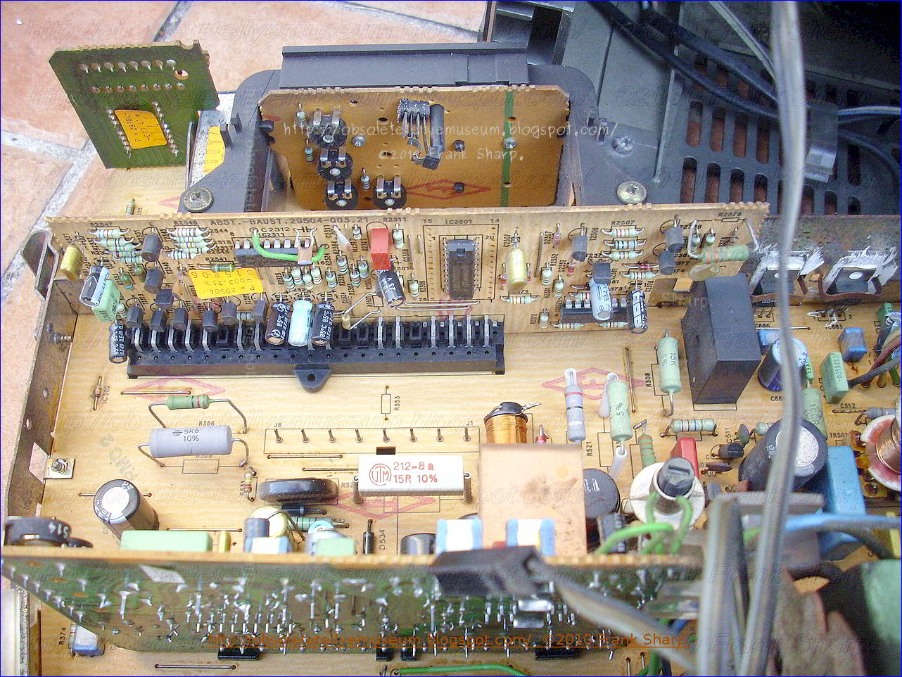
CHASSIS CUC 51KT TUNER UNIT (TUNER BAUSTEIN 29504-001.36)


 TBA120T (Siemens) SIF (Sound IF)


The TUA 2000-4 is a monolithically integrated circuit and suitable as a tuner for the VHF
range up to 400 Mkz, e.g. for TV tuners.
RF section
Few externa! components
Stable oscillator frequency and amplitude with very low interference radiation
Optimal rejection of oscillator and input frequencies at the IF output due to a decoupled
active ring mixer circuit
High interference voltage resistance
High-impedance mixer input, for symmetrical and asymmetrical connections
IF post-amplifier for the UHF IF signal
IF section
@
Optimal cross-talk rejection
@
Large signal-modulation range
@
Low noise figure with wide minimum over large load-impedance range
Circuit description
The TUA 2000-4 contains a symmetrical mixer input, as well as a multiplicative mixer. The
oscillator amplitude is regulated. All oscillator operating currents and voltages are stabilized,
so that the oscillator’s amplitude and frequency are largely independent of temperature
and operating voltage changes.
The IF amplifier has been provided with a high impedance input.
The output has two open collector connections.
During UHF operation, oscillator and mixer are switched off and the UHF IF input coupling
stage is activated.
RF section
Few external components
Stable oscillator frequency and amplitude with very low interference radiation
Optimal rejection of oscillator and input frequencies at the iF output due to a decoupled
active ring mixer circuit
High interference voltage resistance
High-impedance mixer input, for symmetrical and asymmetrical connections
IF post-amplifier for the UHF IF signa!
IF section
@
Optima! cross-talk rejection
@
Large signal-modulation range
@
Low noise figure with wide minimum over large load-impedance range
Pin description
- “Open collector” output of the IF SAW driver
- “Open collector” output of the IF SAW driver
- Input for external reference voltage
- Low-ohmic collector output to the high reference point of a parallel resonant circuit
- High-ohmic base input to the high reference point of a parallel resonant circuit
- Oscillator signal output for counter connection
- GND
- “Open collector” output of the mixer
- “Open collector” output of the mixer
- Supply voltage
- Asymmetrical IF signal input for the UHF IF signal
- Mixer high-impedance differential input
- Mixer high-impedance differential input
- Switching voltage input for the VHF-UHF switch selection
- Asymmetrical signal input of the IF SAW amplifier
- GND
CHASSIS CUC 51KT TUNING UNIT (ABSTIMMUNG BAUSTEIN 29304-003.21).


 TMS1100NLP (Texas Instruments) Ucontroller
TMS3705NI (Texas Instruments) Tuning drive / control.
MCM2802P (Motorola) Tuning Memory
TMS1100NLP (Texas Instruments) Ucontroller
TMS3705NI (Texas Instruments) Tuning drive / control.
MCM2802P (Motorola) Tuning Memory
General
| General Information | The TMS1100 is an expanded memory version of the TMS1000. The TMS1100 doubles the RAM and ROM available in the TMS1000. |
Production | Early 1975 |
Architecture
| Type | Data Word | Address Space | Instructions | Assists | Reg's GP | Reg's Math | Reg's Index | IO Ports | Stack | Interrupts | Memory |
| PMOS, MCU | 4-bit | 1KB | 43 Standard Instructions & 1024 Micro- instructions | NA | 1 | 1 | 0 | "K" Inputs 4 bits parallel, "R" Outputs 11 lines / bits, "O" Outputs 8 bits parallel | 1x10bits | None | ROM 2KB RAM 64B |
Texas Instruments TMS1000
General
| General Information | Texas
Instruments was locked in a race with Intel to create the first
microprocessor. By most accounts Intel won with the 4004, but
there are a few die hard TI fans who say the TMS1000 was first, because
it was the first “computer on a chip” and that the 4004 was just a
calculator chip. Texas Instruments followed the Intel 8080 with the 4-bit TMS1000. So, while Intel was leading the industry in microprocessors, TI led with this industry unique design "a computer on a chip", specifically designed for control and automation purposes. The 1000 was the first MCU (MicroComputer Unit) , which is an MPU (MicroProcessor Unit) with other support chips (such as RAM, ROM, counters, timers, I/O interfaces) integrated on to the same silicon chip. The original 1000 family consists of 6 chips the TMS1000 and TMS1200 are basic chips, the TMS1070 and TMS1270 are high voltage versions to interface to displays, the TMS1100 and TMS1300 provide twice the on-board ROM and RAM. The TMS1000, TMS1070, and TMS1100 are 28-lead packages, the TMS1200, TMS1270, and TMS1300 are 40-lead versions of the same chips (just 200 to the 28-lead chip numbers). In the 80's TI added to the 1000 family. The 28-lead TMS1170 started with a TMS1100 base and added fluorescent display drive capability and expanded memory (2KB ROM). The TMS1370 was the same as the TMS1170 and added 27 I/O lines. An expanded memory group based on the original TMS1000 chips was also created. They were the TMS1400, TMS1470, and TMS1700 (64 Bytes RAM, 4KB ROM). There were 40-lead versions of the TMS1400 and TMS1470, which because the TMS1600 and TMS1670. CMOS versions were also added, denoted with a "C" suffix, such as TMS1200C. The TMS1000 also had system evaluator chips. The original evaluator chips were the TMS1098 and TMS1099. These 64-lead evaluator chips were ROM-less versions of their corresponding standard chips. The TMS1099 supported the TMS1000/TMS1200 and the TMS1070/1270. The TMS1098 supported the TMS1100/1300. Later evaluators were introduced to support the entire TMS1000 family, they were the SE1000P (supports TMS1000,1070,1200,1700), SE2200P (supports TMS1100,1170,1300,1370), and the SE1400P (supports 1400, 1470, 1600, 1670). The success of the the TMS1000 is demonstrated by its long lifecycle (over 20 years) and its expanded product line. The TMS1000 is found in many appliances, control systems, and games. Most of these chips were sourced by companies for direct use in their products and will have custom or house numbers on the chips (not the standard numbers listed above). Even TI used custom numbers in its products. |
GRUNDIG SUPER COLOR C2405 SERIE F3015 CHASSIS CUC51KT Microcomputer processing approach for a non-volatile TV station memory tuning system:
A television tuning system having a non-volatile memory for storing
digital tune words is electrically updated by a microcomputer type
architecture control circuitry. A ROM memory matrix is provided for the
storage of VHF minimum and maximum binary tune words corresponding to
each of twelve VHF channels in addition to a UHF minimum and maximum
binary tune word encompassing all possible 72 UHF channels. Tuning of
individual VHF and UHF chanels is accomplished by incrementing or
decrementing a given tune word within the minimum and maximum limits
established in the ROM memory matrix by means of a microcomputer
processing approach.
TMS1000 General
General Information:
Texas
Instruments was locked in a race with Intel to create the first
microprocessor. By most accounts Intel won with the 4004, but there are a
few die hard TI fans who say the TMS1000 was first, because it was
the first “computer on a chip” and that the 4004 was just a calculator
chip.
Texas Instruments followed the Intel 8080 with
the 4-bit TMS1000. So, while Intel was leading the industry in
microprocessors, TI led with this industry unique design "a computer on
a chip", specifically designed for control and automation purposes.
The 1000 was the first MCU (MicroComputer Unit) , which is an MPU
(MicroProcessor Unit) with other support chips (such as RAM, ROM,
counters, timers, I/O interfaces) integrated on to the same silicon
chip.
The original 1000 family consists of 6 chips the
TMS1000 and TMS1200 are basic chips, the TMS1070 and TMS1270 are high
voltage versions to interface to displays, the TMS1100 and TMS1300
provide twice the on-board ROM and RAM. The TMS1000, TMS1070, and
TMS1100 are 28-lead packages, the TMS1200, TMS1270, and TMS1300 are
40-lead versions of the same chips (just 200 to the 28-lead chip
numbers).
In the 80's TI added to the 1000 family. The
28-lead TMS1170 started with a TMS1100 base and added fluorescent
display drive capability and expanded memory (2KB ROM). The TMS1370 was
the same as the TMS1170 and added 27 I/O lines. An expanded memory
group based on the original TMS1000 chips was also created. They were
the TMS1400, TMS1470, and TMS1700 (64 Bytes RAM, 4KB ROM). There were
40-lead versions of the TMS1400 and TMS1470, which because the TMS1600
and TMS1670. CMOS versions were also added, denoted with a "C" suffix,
such as TMS1200C.
The TMS1000 also had system
evaluator chips. The original evaluator chips were the TMS1098 and
TMS1099. These 64-lead evaluator chips were ROM-less versions of their
corresponding standard chips. The TMS1099 supported the
TMS1000/TMS1200 and the TMS1070/1270. The TMS1098 supported the
TMS1100/1300. Later evaluators were introduced to support the entire
TMS1000 family, they were the SE1000P (supports
TMS1000,1070,1200,1700), SE2200P (supports TMS1100,1170,1300,1370), and
the SE1400P (supports 1400, 1470, 1600, 1670).
The
success of the the TMS1000 is demonstrated by its long lifecycle (over
20 years) and its expanded product line. The TMS1000 is found in many
appliances, control systems, and games. Most of these chips were
sourced by companies for direct use in their products and will have
custom or house numbers on the chips (not the standard numbers listed
above). Even TI used custom numbers in its products. The TMS1000 was
used as a customized chip in the Texas Instruments "Speak and Spell"
educational toy line (See Pictures at bottom).
1. A broadcast receiver tuning system for tuning said broadcast receiver to a selected frequency comprising:
first means for storing digital tune words responsive to a binary address for outputting a selected said digital tune word,
second means for storing said selected digital tune word and said
binary address operably associated with said first means for storing,
a microcomputer operable for selectively changing said digital tune words in said first and second means for storing, and
means for converting said digital tune word stored in said second
means for storing into an analog voltage operative to tune said
broadcast receiver to said selected frequency.
2. A tuning system of claim 1 wherein said microcomputer comprises:
means for incrementing and decrementing said digital tune word stored
in said second means in updating said digital tune word,
means for providing a plurality of operating instructions and logic functions operative of said microcomputer,
means for storing binary data responsive to said binary address and
said instructions operative for incrementing and decrementing said
digital tune word stored in said second means for storing, and
means for inputting control functions operably associated with said means for providing a plurality of operating instructions.
3. A tuning system of claim 1 wherein said means for converting
comprises: a pulse width modulator generator for outputting a digital
signal proportional to said digital tune word, and
a digital to analog converter for converting said digital signal into
said analog voltage for tuning said broadcast receiver to said selected
frequency.
4. A tuning system of claim 1 wherein said broadcast receiver comprises a television set.
5. A tuning system of claim 1 wherein said first means
for storing digital tune words comprises a nonvolatile random access
memory.
6. A tuning system of claim 1 wherein said second means
for storing said digital tune word and said binary address comprises a
shift register.
7. A tuning system of claim 2 wherein said means for
incrementing and decrementing comprises an arithmetic logic unit.
8. A tuning system of claim 7 wherein said arit
TMS1100NLP
a one bit full adder operably associated with said plurality of shift
registers for adding and subtracting said digital tune words and said
binary data stored in said plurality of shift registers, and
means for storing said digital tune words and said binary data operably
associated with said plurality of shift registers and said one bit full
adder.
9. A tuning system of claim 2 wherein said means for
providing a plurality of operating instructions and logic functions
comprises: a program counter,
an instruction memory responsive to said program counter for outputting binary instructions, and
a program logic array responsive to said binary instructions for outputting a plurality of said logic functions.
10. A tuning system of claim 9 further including a
microprogram counter operably associated with said program counter.
11. A broadcast receiver tuning system for tuning said broadcast
receiver to a selected frequency comprising: a first memory matrix  for storing digital tune words corresponding to said selected frequency,
means for generating a binary address for addressing said digital tune word from said first memory,
means for storing said binary address and said addressed digital tune
words operably associated with said first memory and said means for
generating said binary address,
means connected to said address
and tune word storing means for incrementing and decrementing said
addressed digital tune word for updating said digital tune word,
means responsive to said binary address for outputting selected binary
data from a second memory matrix, said binary data used for
incrementing and decrementing said addressed digital tune word,
means connected to said incrementing and decrementing means for
providing a plurality of operating instructions and logic functions
operative for updating said digital tune word,
means for
inputting control functions operably associated with said means for
providing a plurality of operating instructions, and
means for
converting said addressed digital tune word into an analog voltage
operative to tune said broadcast receiver to said selected frequency.
12. A tuning system of claim 11 wherein said digital
tune words further correspond to a plurality of VHF and UHF television
channels.
13. A tuning system of claim 11 wherein said means for
storing said binary address and said addressed digital tune word
comprises a shift register.
14. A tuning system of claim 11 wherein said means for incrementing and
decrementing comprises: a plurality of shift registers,
a one bit full adder operably associated with said plurality of shift
registers for adding and subtracting said digital tune words and said
binary data stored in said plurality of shift registers, and
means for storing said digital tune words and said binary data operably
associated with said plurality of shift registers and said one bit full
adder.
15. A tuning system of claim 11 wherein said means for
providing a plurality of operating instructions and logic functions
comprises: a program counter,
an instruction memory responsive to said program counter for outputting binary instructions, and
a program logic array responsive to said binary instructions for outputting a plurality of said logic functions.
16. A tuning system of claim 11 wherein said means for
inputting logic control functions comprises an input logic status
switch.
17. A tuning system of claim 11 wherein said means for converting
comprises: a pulse width modulator generator for outputting a digital
signal proportional to said digital tune word, and
a digital to analog converter for converting said digital signal into
said analog voltage for tuning said broadcast receiver to said selected
frequency.
18. A tuning system of claim 15 further including a
microprogram counter operably associated with said program counter.
19. A tuning system of claim 14 further including an
automatic channel shift encode for normalization of a binary VHF
increment value comprising one of said binary data stored in said second
memory matrix.
20. A television tuning system for tuning said television to a selected
VHF and UHF channel comprising: a first memory matrix for storing
digital tune words corresponding to said VHF and UHF channels,
means for generating a binary address on a multibus line for outputting said digital tune words from said first memory,
a shift register operably associated with said first memory and said
means for generating a binary address for storing said digital tune word
and said binary address,
an arithmetic logic unit for
incrementing and decrementing said digital tune word stored in said
serial shift register in updating said digital tune word,
means for providing a plurality of operating instructions and logic functions operative in updating said digital tune word,
a second memory matrix for storing binary data used in incrementing
and decrementing said digital tune word, said second memory matrix
responsive to said binary address and said operating instructions, said
second memory matrix also operably associated with said arithmetic logic
unit,
an input logic status switch for inputting control
functions operably associated with said means for providing a plurality
of operating instructions,
a pulse width modulator responsive
to said digital tune word stored in said shift register for outputting a
digital signal proportional to said digital tune word, and
means for converting said digital signal to an analog voltage operative
to tune said television to said selected UHF or VHF channel.
21. A tuning system of claim 20 further including an
automatic channel shift encode for normalization of a binary VHF
increment value comprising one of said binary data stored in said second
memory matrix.
22. A tuning system of claim 20 wherein said means for
providing a plurality of operating instructions and logic functions
comprises: a program counter,
an instruction memory responsive to said program counter for outputting binary instructions, and
a program logic array responsive to said binary instructions for outputting a plurality of said logic functions.
23. A tuning system of claim 22 further including a
microprogram counter operably associated with said program counter.
This invention relates in general to the tuning of a broadcast receiver, and more particularly relates to the tuning of a television receiver using a non-volatile memory for storing binary tuning words that are electrically updated by a microcomputer type architecture control circuitry.
Previously developed electronic channel tuning systems have not been sufficiently flexible to enable wide-spread use for a variety of different types of television sets in applications. For example, certain previously developed systems have required extremely uniform varactor tuning diodes to enable channel tuning, thereby allowing insufficient tolerances for co
nventional variances between
varactor diodes. Other previously developed systems have not been
sufficiently modular to enable a selection of various types of channel
access or displays. Moreover, previously developed electronic channel
tuning systems have not been sufficiently economical to fabricate and
have required uneconomical printed circuit boards or other uneconomical
fabrication techniques for construction. For example, certain prior
systems have required expensive potentiometers for each channel desired
to be tuned. In addition, previously developed electronic television
tuning systems have not satisfactorily satisfied recent regulatory
requirements which call for a television tuner to provide a comparable
capability and quality of tuning for both VHF and UHF stations.
Specifically, such prior tuning systems have not enabled selection of
precise UHF channels, nor have the prior systems provided means for
easily changing selected UHF channels. A major disadvantage in the channel tuning sections of television receivers has been the inability to electronically program and store tune voltages under all operating and non-operating conditions without using an auxiliary power source or a mechanically programmed memory. Existing electronically operable tuners are dedicated electronic circuitry to program tune voltage information in volatile memories where the volatile memories require batteries to provide standby power when the main powe
r source is
removed. The batteries are undesirable because they represent an
additional cost to the manufacturer and a present a long-term tune
voltage jeopardy if they fail when the main power source is removed.
Memory loss due to battery failure can occur if there are poor battery
connections, battery corrosion, or excessive battery drain. Other tuning
systems use potentiometers to retain the channel tune voltage, but are
also undesirable because they are not electronically alterable, and
require a potentiometer for each channel to be tuned.In accordance with the present invention, the undesirable characteristics are eliminated by using a non-volatile DIFMOS memory matrix to store the channel tune voltages. The DIFMOS memory (dual injection floating gate MOS technology) is electronically alterable and has a projected memory retention capability of over 100 years with power removed. The control circuitry for the system uses a microcomputer type architecture to integrate the user control inputs and to generate the signals needed to access and alter the DIFMOS memory matrix. A principal advantage of this type of control compared to the dedicated control circuit approach is the ease with which different manufacturers' system requirements can be satisfied by simply reprogramming the algorithm of the instruction memory.
Accordingly, an object of the present invention is to provide an electronically programmable television tuning system having a non-volatile memory matrix for the storage of binary tune words.
Another object of the present invention is to provide electronic alterable tuning means for a broadcast receiver using a microcomputer approach, thereby eliminating the need for dedicated control circuitry.
Yet another object of the present invention is to provide means for electronically updating binary tune words of a selected channel in the tuning of a television receiver and for storing the updated binary words in a non-volatile memory matrix.
Still a further object of the present invention is to provide a means for generating a binary tune word corresponding to a selected UHF or VHF channel within the limits of a binary minimum and maximum word stored in a memory matrix.
SUMMARY OF THE INVENTION
A television tuning system is taught having a non-volatile RAM memory for storing digital tune words that are electronically updated by a microcomputer type architecture control circuitry. A five-bit binary address word is provided for addressing a 15-bit binary word from a non-volatile memory matrix. The 15-bit binary word comprises 14 bits corresponding to a tune word for the channel selected and a 15th MSB as a skip toggle indicator. The 20 bits are stored in three shift registers in the data in/out circuit in a 5-bit address buffer, a 1-bit skip toggle buffer, and a 14-bit data buffer register. The 14-bit tune word is placed in a data latch comparator for the PWM generator. An analog circuit provides the voltage conversion of the digital output of the PWM generator proportional to the tune word for applying to the varactor tuner of the TV at a selected frequency.
The binary tune word is incremented or decremented to provide an updated tune word in tuning the system by means of a microcomputer approach. The binary tune word is written and read from the non-volatile memory by the same microcomputer system.
The 14-bit binary tune word is updated either by external user control or AFC tuning. In either mode of operation, the tune word is incremented or decremented within a minimum and maximum binary tune word that is stored in a ROM memory matrix. In addition, increment values and tuning time limits are also stored in the ROM memory matrix. An arithmetic logic unit comprising a temporary storage RAM file, two 14-bit working registers, and
a 1-bit full adder provide the means for
performing the system's computations. An 8-bit program counter provides the binary address of instructions in the 8 × 256 instruction ROM which addresses the PLA decode providing for an instruction generator. The PLA decode provides 26 "and" functions and 12 "or" functions. In addition, a 12 to 1 input logic status switch provides the necessary status indication for the 12 external controls. These input signals are detected by a 1-bit status latch.
The system is partitioned into two major functions: the non-volatile memory and the digital to analog converter and control circuits. The channel addressing and varactor diode band selection is generated with a rotary switch assembly. While a rotary switch assembly was used to implement the embodiment, non-volatile memory designs have been generated for addressing and band selection and could be easily implemented. The tune voltage interface between the digital to analog converter and the varactor diodes use standard oscillator and amplifier buffer circuits to provide the AFC summing and UHF tuning functions.
BRIEF DESCRIPTION OF THE DRAWINGS
The novel features believed characteristic of the invention are set forth in the appended claims. The invention itself, however, as well as further objects and advantages thereof, will best be understood by reference to the following detailed description of an illustrated embodiment taken in conjunction with the accompanying drawings, in which:
FIG. 1 is a functional block diagram employed to illustrate the present invention in a TV receiver.
FIGS. 2, 2A-2B are detailed circuit diagrams of the input buffer registers in the data in/out circuit.
FIGS. 3, 3A-3B are detailed circuit diagrams of the ROM constant file and its addressing circuitry.
FIG. 4 is a detailed circuit diagram of the automatic channel shift encode.
FIGS. 5, 5A-5D are detailed circuit diagrams of the instruction ROM, program counter, and microprogram counter.
FIGS. 6, 6A-6D are detailed circuit diagrams of the instruction PLA.
FIGS. 7, 7A-7B are detailed circuit diagrams of the input logic status switch.
FIGS. 8, 8A-8D are detailed circuit diagrams of the arithmetic logic unit.
FIGS. 9, 9A-9B are detailed circuit diagrams of the PWN generator.
FIGS. 10, 10A-10B are detailed circuit diagrams of the analog circuitry.
FIGS. 11A-11H are detailed architecture diagrams of the microcomputer system.
FIG. 12 represents the tune voltage amplifier diagram and related equations for calculating binary words corresponding to tune voltages.
FIGS. 13, 13A-13L are detailed drawings of the instruction set algorithm for the non-volatile stationary memory tuning system.
DETAILED DESCRIPTION
A more complete understanding of the detailed embodiment will be understood by a brief description of the requirements of the system. The fine tune up or down is accomplished by a rocker switch with center off position. A closed position on the switch will increment the tune voltage at the rate of 2 to 8 steps per second. The fine tune control is operative on VHF and UHF tuning modes.
UHF programming is accomplished by pushing a potentiometer control knob and turning the knob pointer to the desired channel number. When the knob is pushed, a contact is switched to ground. The knob is spring loaded in the out position and cannot be turned unless pushed in. The UHF programming potentiometer has approximately 30 turns. The user is able to fine tune a UHF station with this potentiometer and also with a fine tune rocker switch. The UHF fine tune limit is said to be plus or minus 128 steps from the binary word stored in the non-volatile memory RAM matrix only when the fine tune rocker switch is used. If the user continues to hold the rocker switch in the same mode after 128 steps, the tune voltage reverses direction and increments in the other direction for 256 steps until it hits the other limit where it reverses direction again.
Storage and memory requires approximately 240 milliseconds. The binary tune voltage word and skip signal is stored when the set is turned off. If any tuning control for the channel skip button has been engaged while addressing the channel, the tune voltage and
skip will also be stored in
the memory when a channel change occurs. An interchannel AFC defeat pulse occurs between each adjacent channel position. The pulse occurs when a switch contact is momentarily shorted to ground. The duty cycle of the pulse is approximately constant versus the rate of rotation of the channel select knob. The duty cycle is about 25% contact closed and 75% contact open. The binary input address is sampled and latched at the end of a write time or 48-68 milliseconds after receipt of the last interchannel pulse, whichever occurs last. A user programmable skip channel signal output is utilized. The operator uses a pushbutton to change the state of the signal.
The system has been designed for a 20 channel capacity. This includes 12 dedicated VHF channels plus 8 undedicated UHF channels. In VHF mode, a ROM plus non-volatile RAM approach is used to limit fine tuning. The ROM plus RAM make up a 14-bit tuning word plus a 1-bit skip flag. The RAM is 8-bits tuning word plus skip flag. The system is designed such that the LSB of the 8-bit tuning word can be reprogrammed for each VHF channel to occur anywhere from the LSB position to the 7th bit of the 14-bit tuning word. In the UHF mode the RAM shall be 14-bits for the tuning word plus 1 bit for skip flag.
 Referring
now to the block flow diagra
Referring
now to the block flow diagram of FIG. 1, the TV tuning microcomputer approach flow diagram is indicated. The television receiver 2 has a selector switch 26 for generating an address for the non-volatile memory matrix contained in the microprocessor circuitry 4. A more detailed block diagram of the non-volatile memory architecture and address architecture is indicated in FIG. 11A. In one embodiment the non-volatile memory comprises a DIFMOS memory matrix (dual injection floating gate metal oxide semiconductor). Data retention without power is achieved by storing charge on an array of floating gates. Any floating gate in the memory array can be charged or discharged by the injection of electrons or holes from an avalanche plasma formed in two special injector structures within each bit. Once a floating gate has been charged, it will stay charged almost forever, unless it is intentionally discharged by reprogramming. The decay rate of a charge from a floating gate has been measured at less than 1% of the initial value per decade of time at 85° C. In the embodiment described the Texas Instruments X-929A decoded 32 bit non-volatile RAM semiconductor memory is used. However, other non-volatile memories may additionally be used in the present invention.

The channel shift encode is provided to normalize the bit weighting of the increment value for selected VHF channels. The normalized binary word is applied to the microprogram counter to provide shift controls to the various shift registers of the tuning circuitry in the VHF mode.
Input commands by the user is read into the system by means of the input logic and status latch. This provides a means of detecting a change of state on the input switches during a tuning function so that the system may be changed to the latest input command. The change of state is detected by a status latch which loads a new address of the instruction ROM into the program counter.
The program counter provides any one of 256 instruction addresses of the instruction ROM. The instruction ROM addresses the constant memory matrix which contains the upper and lower limits for the VHF and UHF channels, increment values for both VHF and UHF tuning, time increments, write time, and maximum times. In addition, the instruction ROM addresses the instruction PLA which contains decoding for 26 "and" functions and 12 "or" functions.
The ROM constant memory matrix transfers the data to the arithmetic logic unit which contains 2 working registers, a 1 bit full adder and a RAM temporary storage file. The arithmetic logic unit provides for the operation of incrementing and decrementing tune words, providing for write times, and time out functions. The new binary tune word from the arithmetic logic unit is loaded into the data in/out circuitry or read from it. In all aspects of the operation of the present invention, the binary tune word corresponding to the individually selected channel in both the VHF and UHF mode are stored in the non-volatile RAM memory matrix for addressing upon channel selection.


Referring now to FIGS. 2A-2B the data in/out circuitry comprising the input buffer registers is indicated in greater detail. A 5 bit address buffer serial register 230 is provided in addition to 2 D flip flops 232 and 254. A 3 to 1 encode 236 is provided for transmitting of data to the 14 bit input data buffer serial register 234A-234B. Data stored in the input data buffer is parallel loaded into the 14 bit data latch serial register 238A-238B the output of which is parallel loaded into a 14 bit pulse width modulated logic latch serial register. The D flip flop 232 provides as a 1 bit skip toggle buffer for the MSB of the tune word.
A more detailed circuit diagram of the address decode and ROM


constant file is indicated in FIGS. 3A-3B. Five bits from the address generator and 4 bits from the instruction ROM are decoded to address the 32 by 14 bit ROM constant file 264A-264B. The output of the ROM constant file is loaded into a 14 bit B working register.

The instruction ROM, program counter, and microprogram counter circuitry are indicated in greater detail in FIGS. 5A-5D. The 8 by 256 bit instruction ROM 286A-286B is addressed by the 8 bit program counter 290A-290B. The 8 bit program counter is divided into two serial registers comprising 4 MSB's and 4 LSB's. The LSB's are loaded directly from the 8 bit instruction program word from the instruction ROM. The 4 MSB's are loaded into the program counter by means of the 4 bit page latch 294. In addition, 6 bits of the instruction program word are applied to a PLA decode and 4 LSB's of the instruction program word are applied to a 9 by 32 address decode of a ROM constant file. The 8 to 4 encode 302A and 302B is addressed by 4 LSB's from the 8 bit instruction word and 4 bits from an automatic channel shift encode. These 8 bits are encoded to 4 bits which addresses the 4 bit microprogram counter 400. Also, the 4 LSB's from the instruction ROM addresses a 4 to 12 decode for an input logic status switch. Two of the 4 LSB's addresses a 2 to 4 decode of a temporary storage RAM file in the arithmetic logic unit.

FIGS. 6A-6B is a more detailed circuit diagram of the instruction PLA. Six bits of address from the instruction ROM are used to address the 6 by 28 by 12 bit PLA decode. The output of the PLA comprise 26 "and" functions and 12 "or" functions.
 FIGS. 7A-7B is
a more detailed circuit diagram of the input logic status switch. The
12 inputs to the status switch are read by decoding 4 LSB's of
instruction word from an instruction ROM. An indication of a match
between the decode and the 1 of 12 inputs is indicated by the setting of
a status latch 282. This status latch is loaded to the one state in the
presence of any of the 12 input functions and a matching code.
FIGS. 7A-7B is
a more detailed circuit diagram of the input logic status switch. The
12 inputs to the status switch are read by decoding 4 LSB's of
instruction word from an instruction ROM. An indication of a match
between the decode and the 1 of 12 inputs is indicated by the setting of
a status latch 282. This status latch is loaded to the one state in the
presence of any of the 12 input functions and a matching code.


FIGS. 10A-10B are a more detailed circuit diagram of the analog circuit for converting the digital output of the PWM generator of an analog voltage to be applied to the varactor tuner of the television. In addition, circuits for PWM power up clear, AFC defeat, interchannel pulse, and UHF up/down circuitry are provided.
Referring now to the system diag
ram of FIGS. 11A-11H, the TV tuning
microprocessor architecture is indicated in greater detail than the
block diagram of FIG. 1. The 5 bit binary channel address is read off
the 20 position selector switch 202 by means of the address generator
204 in FIG. 11A. The binary address corresponds to any one of 20
channels, 12 of which are VHF channels and 8 of which are UHF channels.
In addition to the channel addressing the selector switch has means for
channel interrupt selection 224, means to select the varactor band of
the TV tuner 226, and means to program AFC bias on and off 228. The
channel address is read directly into the 5 bit address latch 206 in the
non-volatile RAM circuitry. Information in the 5 bit address latch 206
is used to address the 32 bit addressable non-volatile RAM matrix and
also provides a parallel input into a 5 bit address shift register 208.
The 5 bit address on a multibus line from the selector switch is used to
address one of the 20 locations in the non-volatile memory circuitry
used to retain the binary tune word. Provided in the memory circuitry
are 12 VHF binary tune words and 8 UHF binary tune words.
In series with the shift register 208 is a 15 bit data out shift register 210. These two shift registers 208 and 210 are in a read mode when not programmed to shift out. Therefore they are always looking at and reading the address latch 206 and the 15 bits of the memory matrix 212. Fourteen bits of the non-volatile RAM matrix are used for representing the binary tune word and the 15th MSB is used for a skip toggle indicator. The 20 bits comprising 5 from the address register and 15 bits from the data out register are serially shifted out when we read the non-volatile memory 212. As the bits are serially shifted out they are also fed back into the stack in a serial manner by loop 222 so that the 5 bit address and the 15 bit data tune word are restored into the registers.
The address and data tune word as they are shifted out of the registers into the control chip are fed into a 20 bit input data buffer comprising a 5 bit address buffer 230, a 1 bit skip toggle buffer 232, and a 14 bit input data buffer register 234 indicated

The binary tune word in data buffer register 234 is loaded parallel into the 14 bit PWM logic latch 248 when there is a load PWM (LPWM) signal on the 14 bit data latch 238. The 14 bit tune word in the PWM logic latch 248 is used as a compare word for the 14 bit pulse width modulator counter 250. The pulse width modulator operates with a 1 MHz input clock from the PWM buffer and oscillator 252 that is fed into the 214 PWM counter 250 and runs continuously.
The
PWM counter 250 counts from binary 0 in a binary manner until it
reaches one of two conditions. First, if the binary word of the counter
250 compares with the 14 bit tune word in the PWM logic latch 248 then
the PWM logic latch which is performing a magnitude compare will provide
an output signal and trip a flipflop which will then remain in that
state until the counter completes its count-out cycle. The second
condition is when the PWM logic latch 248 is at an all 1 state whereby
the PWM counter would count up to an all 1 state that also corresponds
to the runover point of the counter. Therefore, the PWM counter will
always count up to 214 and then run over where 214 and a 1 MHz input corresponds to a writeout at 16 milliseconds. In the PWM generator we therefore have a magnitude compare of the PWM counter with the 14 bit tune word stored in the 14 bit PWM logic latch 248 and when the first time there is a match of the counter and the binary magnitude we receive an output signal from the PWM logic latch 248 proportional to the tune word. To tune the television we alter the pulse width modulated signal from the PWM logic latch 248. We alter the pulse width modulated signal by changing the bit value of the binary tune word contained in the PWM logic latch thereby giving us a modulated pulse width at a duty cycle of 16 milliseconds.
The skip toggle bit in the skip toggle buffer register 232 may be altered by means of the skip toggle inputs through the MAND gate 256. In the program algorithm when the skip toggle is altered we read the information out and write it into memory once the function is complete. Altering of the skip toggle information is achieved by first reading the state of the skip toggle buffer 232 which contains an MSB that was read out of memory, loading that bit into a D register 254, and changing that information if we have a program input to change the state of the skip toggle. A skip toggle output 258 is provided to give an indication that the skip toggle has been altered and the present program condition of the skip toggle. The skip toggle is not applicable to a mechanical rotary type selector switch system as indicated in this embodiment whereas the selector switch 202 is of a rotary type. However, by replacing the rotary selector switch with an electronically addressable circuit as disclosed in U.S. Pat. No. 3,968,443 issued on July 16, 1976, assigned to Texas Instruments Incorporated, the same assignee of the present patent application, then a skip function would be applicable in the present tuning circuitry.
After loading the address buffer 230 with the 5 bits of address from the address generator 204 these 5 address bits are transferred in a parallel mode to the 9 by 32 address decode 260 and the 5 to 4

automatic channel shift encode (VHF only) 262 indicated in FIG. 11C. The automatic channel shift encode is used to determine whether the system is functioning in the UHF or VHF mode. If the system is functioning in the VHF mode the automatic channel shift encode provides one of four possible codes for incrementing the VHF tune word. The four codes corresponding to the particular incrementing bit value that applies to the VHF channel that has been selected by the address generator 204. Since there are only four increment rate values and 12 VHF tune words, the encode 262 selects depending upon which channel the system is on one of the four incrementing rate values to be applied to the given tune word.
The 5 bit address from the address buffer 230 is also parallel applied to the 9 by 32 address decoder 260 to select a 14 bit data word stored in the ROM constant file 264. The 5 bit address which determines the VHF or UHF channel is decoded by the 9 by 32 address decoder into a 32 bit address word to address the 32 by 14 ROM constant file. The four LSB's of the instruction code determines which of the 32 words we are addressing. These 32 fourteen bit words in the ROM constant file comprise upper and lower limits for the VHF channels, UHF channel limits, increment values for both VHF and UHF tuning, time increments, maximum times, and write time.
When we have read a tune word into the input data buffer 234 and want to perform a tuning function upon it, we transfer the 14 bits of data out of the input data buffer register and into the 14 bit A working register 266 by means of a read input data buffer (RIBD) command at the 4 to 1 encode switch 270. Also, the 14 bit word is serially transferred back into itself by means of loop 272. After loading register A with the 14 bit tune word, the tune limit and increment value is outputted from the 14 bit ROM constant file and loaded into the 14 bit B working register 274. These values are now loaded into the temporary storage RAM file 276 by selection of the LBMX command on the selector switch encode 278. The temporary storage file comprises a 4 by 14 bit RAM file. Tuning is now performed by adding an increment value which is stored in register B to the 14 bit tune word stored in register A if the system is in a tuned upmode and subtracting them if the system is in a tuned downmode.

The incremented or decremented tune word is restored into the A working register by means of the "A" normalize command on the selector switch encode 270 indicated in FIG. 11D.
After the restore operation the updated 14 bit tune word is transferred into the input data buffer 234 by performing a load input data buffer (LIDB) command on selector switch encode 236. The updated tune word is now stored into the input data buffer and also restored into register A. The updated tune word is now loaded into the 14 bit PWM logic latch 248 whereby the PWM counter 250 can compare its out to updated tune word.
Whenever a tuning function is performed the system goes through a sequence whereby it performs an addition and a time out routine in the arithmetic logic unit by decrementing our timing word until a negative number is reached. In each case information is read from the ROM constant file and stored into the temporary storage RAM file. This information is a function of the particular channel and whether the channel is a UHF or VHF channel. In the sequence the system always goes through reading the input switches so if there is a change of state on our input switches during a tuning function it will be detected and the system function will be changed to the latest input command.

These input control functions are read into the system by means of the 12 to 1 input logic status switch 280 having 12 inputs indicated in FIG. 11F. A 61 kilohertz slow clock is provided to perform the write function which in the case of the non-volatile memory comprising DIFMOS memory cells takes in the order of 100 milliseconds to write a 0 into the memory, therefore requiring a clock running at a slower rate then the control or processing clock that is normally used. The slow clock is also used to provide dampening when in the power up mode or after we have already completed a write command in writing into memory so that the system doesn't read the new word while it is still settling.
Another input is the UHF/VHF control line that is a function of the particular address that has been detected from our selector switch 202. A third and fourth input is an AFC high and an AFC low select. The function of the AFC high/low is to provide a digital AFC control function. The means of achieving the digital AFC control is not indicated in the figures or represented in the algorithm. However, the digital AFC control system could be incorporated into the architecture by means of a couple of comparator windows and the appropriate addition of control logic to the present algorithm.
A fifth input is a UHF up/down control that is a control from a comparator 282 that determines whether the tune voltage is above or below the corresponding potentiometer setting of the UHF channel coarse tune potentiometer 284. An additional input is a power on/off select. Upon a power down input the 14 bit tune word stored in the input data buffer register 234 is written into the addressable non-volatile memory.
The seventh input is a skip toggle input which is not incorporated into the present system. This skip function if made available would allow for the skipping over of selected channels but is not applicable to a mechanical rotary switch as noted above.
The eighth and ninth inputs comprise the rocker arm fine tuneup and fine tunedown for the control voltage. The UHF tune on/off control places the tuning function into a coarse U
HF tuning mode. The AFC on/off switch is used to activate the
internal AFC tuning function or to allow for the external manual tuning
mode. The final switch on the input logic status switch is the
interchannel pulse that is inputted from the selector switch 202 by
means of the channel interrupt line 224. The interchannel pulse provides
an indication that the selector switch is in between channels in a
changing mode and also detects the completed change. The twelve inputs are read into the input logic status switch. If one of the twelve logic status switches is activated it is compared with a particular select code and if there is any indication of a match on the read command of that given instruction to the particular switch being closed or opened as the case may be, the status latch flip-flop 282 is set. The status switch inputs are decoded by the 4 to 12 decoder 284 which is addressed by four LSB's of instruction from the instruction ROM 286. The status latch 282 provides an indication that the system has received an input corresponding to one that has been coded in the instruction table of the decoder 284.
The second input to the status latch 282 is the carry input from the one bit full adder when the system is in a subtract routine and if the subtract routine results in a negative number. The negative number indication is used to perform compare tests to determine whether an upper or lower tuning limit or timing limit has been reached. The setting of the status latch 282 provides an input to the instruction ROM 286 to load the program counter with a new page of instruction address.

The eight bit program counter 290 indicated in FIG. 11C receives its count clock input from the 250 kilohertz clock 292 which is a one quarter division of the one megahertz clock from the PWM counter 250. The program counter gives any one of 256 instruction addresses for the instruction ROM 286. The location of the program counter in its counting sequence may be altered by loading in a new eight bit word into the program counter. The four LSB's from the instruction ROM are parallel loaded into the four LSB positions of the eight bit program counter and parallel loaded into a four bit page batch 294. If the status latch is set by a subtract operation from reading an input from the logic status switch, then upon a load page command (LPD) applied to the NAND gate 296 the four LSB bits of address with be loaded from the page latch into the program counter in the MSB position.
The output of the instruction ROM 286 feeds into the instruction PLA circuitry 298 which outputs 26

The four bit microprogram counter 300 is used to provide shift controls to the various shift registers of the tuning circuitry. And more particular, the microprogram counter allows for the shifting of the 14 bit data word in working register A into the input data buffer register. In addition it allows for the addition and subtraction of working registers A and B and also allows for the transfer of data to the non-volatile memory.
The maximum number of serial shifting by the microprogram counter is 14 bits. When the shifting produced by the microprogram counter is completed, the system operation is returned to the eight bit program counter where it is indexed to the next address in the program. The eight bit microprogram instruction is selected by the microprogram address select encode 302. Four bits from the automatic channel shift encode 262 and four LSB's from the instruction ROM are loaded parallel into the address select encode to provide four bits of instruction address for the microprogram counter 300.

Referring to FIG. 11D a switch encode 304 is provided to allow for a restore operation whereby the 14 bit word in the B working register is shifted back into itself. In addition the switch encode provides for a shifting of the 14 bit word from the temporary storage RAM file 276 into the working register. Switch encode 270 allows for the shifting of a 14 bit word into the A working register from the temporary storage RAM file, the input data buffer register 234, a sum product from the addition of working register A and register B by means of the one bit full adder 288, and finally the restore of the word in the A register into itself.
The temporary storage RAM file 276 is addressed by two bits from the instruction ROM through a 2 to 4 encode 306. The four bit word from the encode is used to select one of four 14 bit storage files in the RAM file 276 by means of the 4 to 1 selector encode 308.
The pulse width modulated output 310 from the PWM logic latch is fed into the PWM buffer 252.

The PWM signal from the PWM buffer is fed into a driver buffer 312 that is referenced to +5 volts in FIG. 11H. The PWM output continues through a three stage PWM filter to provide the IC filtering required for the resolution and ripple voltage needed for a pulse width modulated signal of the longest duration to an acceptable level in the UHF mode. The VHF mode would not need as much filtering to generate a PWM at an acceptable ripple level. However, at least three stages are required for UHF filtering.
The output of the three stage filter is a DC voltage that is proportional to the pulse width modulated signal, the pulse width modulated signal being proportional to the 14 bit tune word that has been loaded into the 14 bit input data buffer register and PWM logic latch. The tune voltage is amplified by inverting voltage amplifier 316 and subsequently filtered by an additional single stage filter 318. The final DC analog tune voltage is passed to the television varactor tuner for tuning to the selected channel.
A second comparator 282 comprises a UHF up/down comparator which receives its inputs from the three stage PWM filter and a UHF course tune potentiometer 284. The potentiometer is referenced to the same +5 volts as the driver buffer 212. The comparator 282 provides an indication as to whether or not the system is in the coarse tune mode of UHF, whether or not the system is above or below the desired tune voltage for the particular channel setting, and provides a coarse tuning signal for the controller.
FIG. 320 represents the power supply required for the operation of the tuning syst
em. The +5 volts used to provide the upper
voltage for the tuning amplifier for the varactor tune voltage output.
The +17 volts is used for biasing of the MOS circuitry of the
non-volatile memory. The +10 volts is used for biasing the CMOS logic in
the system. The +5 volts is used for the TTL and I2 L logic
in the system. Finally, the 0 to -35 switch voltage is used for
programming the non-volatile memory when the system is in a write mode. In performing a tuning function using the microcomputer approach in the VHF mode a binary tune word that is stored in the input data buffer register is incremented or decremented within the limits for the minimum and maximum tune voltages for the selected channel that is stored in the ROM constant file. The ROM constant file contains a binary word for the maximum tune voltage and minimum tune voltage for each of the 12 VHF channels. These limits establish the range of tuning permitted by the system. These values are individually selected for each of the VHF channels. In a similar manner minimum and maximum limits are established for the UHF channel. However, due to the large number of UHF channels the minimum and maximum limit are established so as to encompass all 72 UHF channels with tuning for the selected UHF channel falling therebetween.
Referring now to FIG. 12 the schematic diagram used for calculating the minimum and maximum tune voltages is indicated in addition to the equations used. Equation 3 is the input voltage as a function of the output tune voltage. Given the desired tune voltage EO the input voltage Ei may be calculated. In addition, by using equation 4 the bits corresponding to the input voltage is calculated thereby resulting in the binary tune word corresponding to the calculated input voltage.
In this regard, Table I indicates the VHF ROM constants for the minimum limits as established by equations 3 and 4. Each of the VHF channels have a unique binary word corresponding to the minimum voltage limit. In a similar manner Table II indicates the VHF ROM constant for the maximum tune voltage. As noted the nominal tune voltage for tuning the television will lie somewhere between these two established limits. The binary words comprise 14 data bits and are addressed by the 5 bit binary address from the selector switch.
| TABLE I |
| __________________________________________________________________________ |
| VHF ROM CONSTANTS (MINIMUM) NOM MAX MIN CH# EAFC Eo Ei BITS 8192 4096 2048 1024 512 256 128 64 32 16 8 4 2 1 |
| __________________________________________________________________________ |
2 1.549 2.149 1.442 4725 0 1 0 0 1 0 0 1 1 1 0 1 0 1 3 1.814 4.320 1.367 4479 0 1 0 0 0 1 0 1 1 1 1 1 1 1 4 2.310 7.158 1.444 4731 0 1 0 0 1 0 0 1 1 1 1 0 1 1 5 4.589 23.000 1.301 4263 0 1 0 0 0 0 1 0 1 0 0 1 1 1 6 4.528 29.885 0- 0- 0 0 0 0 0 0 0 0 0 0 0 0 0 0 7 2.299 7.550 1.361 4459 0 1 0 0 0 1 0 1 1 0 1 0 1 1 8 2.490 9.440 1.249 4092 0 0 1 1 1 1 1 1 1 1 1 1 0 0 9 2.726 11.790 1.107 3627 0 0 1 1 1 0 0 0 1 0 1 0 1 1 10 3.021 14.710 0.934 3060 0 0 1 0 1 1 1 1 1 1 0 1 0 0 11 3.594 18.370 0.955 3129 0 0 1 1 0 0 0 0 1 1 1 0 0 1 12 4.049 23.000 0.665 2179 0 0 1 0 0 0 1 0 0 0 0 0 1 1 13 4.621 29.920 0.103 337 0 0 0 0 0 1 0 1 0 1 0 0 0 1 |
| __________________________________________________________________________ |
| TABLE II |
| __________________________________________________________________________ |
| VHF ROM CONSTANTS (MAXIMUM) NOM MIN MAX CH# EAFC Eo Ei BITS 8192 4096 2048 1024 512 256 128 64 32 16 8 4 2 1 |
| __________________________________________________________________________ |
2 1.549 0.400 1.754 5747 0 1 0 1 1 0 0 1 1 1 0 0 1 1 3 1.814 0.888 1.979 6484 0 1 1 0 0 1 0 1 0 1 0 1 0 0 4 2.310 2.149 2.339 7664 0 1 1 1 0 1 1 1 1 1 0 0 0 0 5 4.589 4.682 4.572 14,980 1 1 1 0 1 0 1 0 0 0 0 1 0 0 6 4.528 12.260 3.147 10,311 1 0 1 0 0 0 0 1 0 0 0 1 1 1 7 2.299 4.624 1.884 6173 0 1 1 0 0 0 0 0 0 1 1 1 0 1 8 2.490 6.010 1.861 6098 0 1 0 1 1 1 1 1 0 1 0 0 1 0 9 2.726 7.550 1.865 6111 0 1 0 1 1 1 1 1 0 1 1 1 1 1 10 3.021 9.440 1.875 6144 0 1 1 0 0 0 0 0 0 0 0 0 0 0 11 3.594 11.790 2.130 6979 0 1 1 0 1 1 0 1 0 0 0 0 1 1 12 4.049 14.710 2.145 7028 0 1 1 0 1 1 0 1 1 1 0 1 0 0 13 4.621 18.370 2.166 7097 0 1 1 0 1 1 1 0 1 1 1 0 0 1 |
| __________________________________________________________________________ |
The data including the VHF minimum and maximum limits are stored in the ROM constant file as indicated in Table III. As noted the ROM constant file has 32 separate data values stored therein. The VHF and UHF increment values are also stored in the ROM constant file. The maximum time for both VHF tuning and UHF tuning are also stored therein. In addition, the time increment value is also stored. Finally, the UHF minimum tune word and the UHF maximum tune word including the write time is stored in the ROM constant file.
| TABLE III |
| ______________________________________ |
| ROM CONSTANT FILE Add- Prom ress Code Instruction No. Binary Msb Lsb |
| ______________________________________ |
# 2 VHF MIN 0 00000 0 010 0100 0 111 0101 # 2 VHF MAX 1 00001 0 010 1100 0 111 0011 # 3 VHF MIN 2 00010 0 010 0010 0 111 1111 # 3 VHF MAX 3 00011 0 011 0010 0 101 0100 # 4 VHF MIN 4 00100 0 010 0100 0 111 1011 # 4 VHF MAX 5 00101 0 011 1011 0 111 0000 # 5 VHF MIN 6 00110 0 010 0001 0 010 0111 # 5 VHF MAX 7 00111 0 111 0101 0 000 0100 # 6 VHF MIN 8 01000 0 000 0000 0 000 0000 # 6 VHF MAX 9 01001 0 101 0000 0 100 0111 # 7 VHF MIN 10 01010 0 010 0010 0 110 1011 # 7 VHF MAX 11 01011 0 011 0000 0 001 1101 # 8 VHF MIN 12 01100 0 001 1111 0 111 1100 # 8 VHF MAX 13 01101 0 010 1111 0 101 0010 # 9 VHF MIN 14 01110 0 001 1100 0 010 1011 # 9 VHF MAX 15 01111 0 010 1111 0 101 1111 #10 VHF MIN 16 10000 0 001 0111 0 111 0100 #10 VHF MAX 17 10001 0 011 0000 0 000 0000 #11 VHF MIN 18 10010 0 001 1000 0 011 1001 #11 VHF MAX 19 10011 0 011 0110 0 100 0011 #12 VHF MIN 20 10100 0 001 0001 0 000 0011 #12 VHF MAX 21 10101 0 011 0110 0 111 0100 #13 VHF MIN 22 10110 0 000 0010 0 101 0001 #13 VHF MAX 23 10111 0 011 0111 0 011 1001 VHF INCRE- 24 11000 0 000 0000 0 100 0000 MENT TIME INCRE- 25 11001 0 000 0000 0 000 0001 MENT MAX TIME 26 11010 0 000 0101 0 000 1100 (ROCKER) UHF INCRE- 27 11011 0 000 0001 0 001 0101 MENT UHF MIN V 28 11100 0 000 0000 0 010 0000 UHF MAX V 29 11101 0 111 0100 0 101 0110 WRITE TIME 30 11110 0 000 1100 0 001 1011 MAX TIME 31 11111 0 000 0000 0 010 1000 (UHF) |
| ______________________________________ |
Table IV indicates the PLA logic for automatic right shift addressing (VHF only) of the microprogram counter. As noted from Table III the VHF increment value has a 1 in the 7th bit position. During the incrementing or decrementing of the VHF word it is desired to increment or decrement at a particular bit weight value unique to each of the VHF channels. To accomplish this, the automatic channel shift encode provides for right shifting of the increments value so as to normalize it to provide a different bit weight for each of the 12 UHF channels. The number of right shift in the VHF mode for each of the selected channels is indicated in Table IV in addition to the encode word for the microprogram counter preset. Since the UHF tuning is performed by a process which provides for the increasing of the bit weight of the increment value, the normalization by right shifting the increment value is not needed.
| TABLE IV |
| ______________________________________ |
| PLA LOGIC FOR AUTOMATIC RIGHT SHIFT ADDRESSING (VHF ONLY) OF μ PROGRAM COUNTER No. of Right Encode Word For VHF Channel Shifts For For μ Program No. Binary Word Normal Ration Counter Preset |
| ______________________________________ |
2 00000 4 1011 3 00001 3 1100 4 00010 2 1101 5 00011 1 1110 6 00100 0 1111 7 00101 3 1100 8 00110 3 1100 9 00111 3 1100 10 01000 3 1100 11 01001 2 1101 12 01010 2 1101 13 01011 2 1101 UHF 01100 10100 0 N.A. |
| ______________________________________ |
The instructional logic from the PLA decode is indicated in Tables V and VI. In Table V the instruction ROM decode outputs comprising 12 NOR gate outputs is indicated. These 12 outputs provide the "OR" logic functions for the microcomputer program. Table VI indicates the 28 instruction ROM decode outputs of the PLA decode. These outputs comprise 28 "AND" logic functions for the microcomputer programming.
TABLE V
INSTRUCTION
ROM DECODE OUTPUTS
(NOR GATE OUTPUTS)
1. lpc = ubrn + brn s/l
2. μpc enable = rnvm + lnvm + rsax + rsbx + add + suba + subb + rmxa + rmxb + lamx + lbmx + nora + norb + resa + resb + ridb + lidb + wro + wri + 27 bit (of p.c.)
3. ld μpc = rnvm + lnvm + rsax + rsbx + nora + norb + resa + resb
4. data in sel idb = shift cont. in code = rnvm + lnvm
5. shift cont. idb = ridb + rnvm + lnvm + lidb
6. shift cont. ram = rmxa + rmxb + lamx + lbmx
7. ram data restore sel = rmxa + rmxb
8. shift cont. reg a = rmxa + lamx + rsax + add + suba + subb + nora + resa
9. reg a sel restore a = resa + lamx + lidb
10. reg a sel Σ = add + suba + subb
11. shift cont. reg b = rmxb + lbmx + rsbx + add + suba + subb + norb + resb
12. reg b sel restore b = resb + lbmx
table vi
instruction
rom decode outputs
(nand gate outputs)
0. unconditional branch (ubrn)
a. if s/l = 1 or 0 (i.e. DON'T CARE)
1. parallel loads program counter on clk with contents of page latch and 4 lsb's of ubrn code.
2. clears s/l on clk
1. branch (brn)
a. if s/l = 1
1. parallel loads program counter on clk with contents of page latch and 4 lsb's of brn code.
2. clears s/l on clk
b. if s/l = 0
1. do nothing
2. load page (ldp)
a. load 4 bit address code into page latch (4 msb's of address).
3. read rom (rrom)
a. parallel loads reg. b with contents of rom stored at location defined by 4 bit address code and/or channel select code (if vhf).
4. read inputs (rin)
a. enables input defined by 4 bit address to be gates thru to the s/l flip/flop. if input is "0" then s/l is loaded with a "1" on clk. if input is a "1" then s/l is loaded with a "0" on clk.
5. read channel code sw. (rccs)
a. sets input strobe to a "1" level so that the channel select switch can be parallel loaded into the nvm latch buffer on the memory ic.
6. load pwm (lpwm)
a. parallel loads the contents of the input data buffer register into the pwm data register during clk.
7. sense nvm (snvm)
a. sets sense line to "0" so that the contents of the nvm can be parallel loaded into the data buffer registers on the memory ic during clk.
***the following functions enable the μ program counter***
8. read nvm buffer (rnvm)
a. selects 4 bit address code to be loaded into μ program counter.
b. loads 4 bit address (0101) into μ program counter to reset it for 10 right shift functions. load occurs during clk.
c. on clk the program counter is disabled, and the μ program counter is enabled.
d. a right shift command is provided for the input buffer registers and the nvm buffer registers until the μ program counter reaches the 1111 state (10 shifts).
e. when the μpc is 1111 then on the next clock pulse (which sets the μpc to 0000) the clk input to the μpc is disabled, and the clk input to the program counter is restored.
f. note: this command sets the data select line to the memory ic to a logic "1" level, so that data can be sequenced out of the ic into the dac.
9. load nvm buffer (lnvm)
a. same as read nvm buffer except sequence (f) is: note: this command sets the data select line to the memory ic to a logic "0" level, so data can be sequenced into the memory ic from the dac ic.
10. right shift a (r.s.a. x)
11. right shift b (r.s.b. x)
a. selects 4 bit variable address code to be loaded into μ program counter.
b. loads μ program counter during clk.
c. disables program counter on clk.
d. enables μ program counter on clk.
e. enables data shift in (a) or (b) register. data in register (a) or (b) is with leading zero's during μ program count time then right shifted according to the following shift code.
| ______________________________________ |
| code right shift operations |
| ______________________________________ |
0000 14 0001 14 0010 13 0011 12 0100 11 0101 10 0110 9 0111 8 1000 7 1001 6 1010 5 1011 4 1100 3 1101 2 1110 1 1111 0 |
| ______________________________________ |
f. when μpc is 1111 THEN ON NEXT CLK PULSE THE μPC CLK INPUT IS DISABLED AND THE PC CLK IS ENABLED.
12-1 add (a & b) (add)
a. program counter is disabled on clk.
b. μpc is enabled on clk.
c. shift controls to reg. a and reg. b are enabled.
d. reg. b restore sel. is enabled.
e. reg a Σ input select is enabled.
f. when μpc is 1111 THE μPC CLK IS DISABLED AND THE PC IS ENABLED.
12-2,3 subtract (b-a) (suba) subtract (a-b) (subb)
a. enables inverter input to adder (e) from reg. a or reg. b.
b. sets carry bit in e1 to "1".
c. pc is disabled on clk.
d. μpc is enabled on clk.
e. reg a and reg b shift control is enabled.
f. data is shifted serially from reg a and reg b into Σ.
g. data in reg b is restored into reg b without change.
h. Σ data out is stored in reg a.
i. when μpc is 1111 THEN PC IS ENABLED AND μPC IS DISABLED.
13-1 read ram ➝ a (rmxa)
read ram ➝ b (rmxb)
a. address bits (2 bits) select ram storage location.
b. control enables ram read storage gate.
c. control enabled ram ➝ a or ram ➝ b select.
d. pc is disabled on clk.
e. μpc is enables on clk.
f. ram & reg a or reg b shift gates are enabled.
g. data is shifted from ram to reg a or b until μpc is 1111 then μpc clk is disabled and pc clk is enabled.
13-3 load a ➝ ram (lamx) 1,2,3,4
load b ➝ ram (lbmx) 1,2,3,4
a. program counter is disabled on clk.
b. μpc is enabled on clk.
c. address bits (2 bits) select ram storage location.
d. shift controls for selected memory location are enabled.
e. reg a ➝ m sel. and REG A DATA RESTORE.
14-1 normalize a (nora)
14-2 normalize b (norb)
a. selects 4 bit channel encode address to be loaded into μpc (normalized code).
b. loads 4 bit channel encode address into μpc during clk.
c. pc is disabled on clk.
d. μpc is enabled on clk.
e. control enable shift gates of reg. a or b.
f. control sets reg. a and reg. b inputs (serial) to "0".
g. data is shifted in reg. a or b until μpc is 1111 then μpc clk is disabled & pc clk is enabled.
14-3 unused code
14-4 slow clock enable (sloc) switches the clock input to the μpc from t1 clock line to the slow clk line (16ms PERIOD).
15-1 read input data buffer (ridb)
a. enables buffer data select into reg a.
b. enables input buffer data restore select gate into data buffer.
c. enables input data buffer and reg. a data shift control.
d. pc is disabled on clk.
e. μpc is enabled on clk.
f. data is shifted from data buffer into reg. a until μpc is 1111, μpc is disabled and pc is enabled.
15-2 load input data buffer (lidb)
a. enables reg. a data select gate into data buffer reg.
b. enables restore select gate into reg. a.
c. control enables reg. a and INPUT DATA BUFFER SHIFT GATE.
D. pc is disabled on clk.
e. μpc is enabled on clk.
f. data is shifted from reg. a to data buffer until μpc is 1111, then μpc is disabled and pc is enabled.
15-3 clear write (cwro) resets the sense line to the memory ic to a "1"; switching the memory cells from a write mode to a read mode.
15-4 write (wro) sets the sense line to "0" on clk; thereby permitting data to be written into the memory ic cells.
15-5 dummy (unused) unused code used for dummy operations.
the op-codes for the single clock instructions including their address are indicated in Table VII.
| TABLE VII |
| ______________________________________ |
| OP-CODES SINGLE CLOCK INSTRUCTIONS FUNCTION OP-CODE ADDRESS |
| ______________________________________ |
UBRN 0000 1/0 1/0 1/0 1/0 BRN 0001 1/0 1/0 1/0 1/0 LDP 0010 1/0 1/0 1/0 1/0 RROM 0011 1/0 1/0 1/0 1/0 RIN 0100 1/0 1/0 1/0 1/0 RCCS 0101 X X X X LPWM 0110 X X X X SNVM 0111 X X X X |
| ______________________________________ |
The 4 bit and 6 bit op-codes for the microprogram control instructions including their addresses are indicated in Table VII.
| TABLE VIII |
| ______________________________________ |
| OP-CODES MICROPROGRAM CONTROL INSTRUCTIONS OP- FUNCTION CODE ADDRESS |
| ______________________________________ |
RNVM 1000 1/0 1/0 1/0 1/0 4 BIT LNVM 1001 1/0 1/0 1/0 1/0 OP-CODE RSAX 1010 1/0 1/0 1/0 1/0 RSBX 1011 1/0 1/0 1/0 1/0 LIDB 110000 -- -- 0 0 ADD 110001 -- -- X X SUBA (B-A) 110010 -- -- X X SUBB (A-B) 110011 -- -- X X RMXA 110100 -- -- 1/0 1/0 RMXB 110101 -- -- 1/0 1/0 6 BIT LAMX 110110 -- -- 1/0 1/0 OP-CODE LBMX 110111 -- -- 1/0 1/0 NORA 111000 -- -- X X NORB 111001 -- -- X X UNUSED 111010 -- -- X X SLOC 111011 -- -- 1 1 RIDB 111100 -- -- 0 0 CLR WRO 111101 -- -- 1 1 WRO 111110 -- -- X X DUMMY 111111 -- -- 1 1 |
| ______________________________________ |
The input control line read codes are indicated in Table IX. The input functions each have the same 4 MSB's (0100) and differ only in the 4 LSB's.
| TABLE IX |
| ______________________________________ |
| INPUT CONTROL LINE READ CODES RIN CODE INPUT FUNCTION 4 MSB'S 4 LSB'S |
| ______________________________________ |
UNUSED 0100 0000 CHANNEL INTERRUPT 0100 0001 AFC ON/OFF 0100 0010 UHF ON/OFF 0100 0011 FINE TUNE UP 0100 0100 FINE TUNE DWN 0100 0101 SKIP TOGGLE 0100 0110 UHF/VHF 0100 0111 POWER ON/OFF 0100 1000 UHF UP/DWN 0100 1001 AFC HI 0100 1010 AFC LO 0100 1011 SLOW CLOCK 0100 1100 UNUSED 0100 1101 UNUSED 0100 1110 UNUSED 0100 1111 |
| ______________________________________ |
The ROM constant address codes are indicated in Table X. It is to be noted that the 12 VHF channels are encoded to 12 minimum limits and 12 maximum limits and use the first 24 ROM addresses (00000 to 10111). The remaining 8 words are located in the last 8 ROM addresses (11000 to 11111), thus using a 32 word by 14 bit ROM structure. A greater understanding of the tuning system and the information contained in Tables I-X is gained by referring to the instructions set algorithm.
| TABLE X |
| ______________________________________ |
| ROM CONSTANT ADDRESS CODES RROM CODE STORED WORD (14 BITS) 4 MSB'S 4 LSB'S |
| ______________________________________ |
VHF MIN LIMIT 0011 00XX VHF MAX LIMIT 0011 01XX VHF INCREMENT 0011 1000 TIME/UHF INCREMENT 0011 1001 MAX FINE TUNE TIME 0011 1010 UHF CHANNEL LIMIT 0011 1011 UHF MIN BAND LIMIT 0011 1100 UHF MAX BAND LIMIT 0011 1101 WRITE TIME 0011 1110 MAX UHF COARSE TUNE TIME 0011 1111 |
| ______________________________________ |


Rocker Tune loop that is the channel fine tuning mode FIGS. 13G-13H, and the fourth loop is the UHF Pot Tune loop comprising the UHF coarse tuning mode FIGS. 13I-13L.

The tuning system is activated by a power up entry 1 in FIG. 13A followed by a load page command (LDP) where a 4 bit address code is loaded into the page latch 294 to address one of the 16 pages in the instruction ROM 286. A clear write (SWRO) operation is performed to reset the sense line to the memory IC to switch the memory cells from a write mode to a read mode. A read channel interrupt loop is performed whereby the system reads the channel interrupt switch until the channel interrupt indication is no longer present.


A channel interrupt indication 224 from the selector switch 202 is applied to the input logic status switch 280. When the input signal matches a 12 bit binary decode 284 the status latch 282 is set. The read channel interrupt loop continuously reads the status latch to determine whether or not it has been set. As long as the status latch has been set from an indication of a channel interrupt the system will loop back into the read mode and will continue until the signal in the status latch is eliminated by the completion of a channel selection at the selector switch 202. The purpose of the channel interrupt read operation is to prevent the system from reading the channel tune word when the selector switch is being changed from one channel to another.
Upon jumping out of the read channel interrupt loop a read channel code switch (RCCS) is performed whereby the five bit address from the selector switch and address generator is parallel loaded into the nonvolatile memory address latch buffer 206 of the memory IC. A slow clock enable signal provides dampening to offset any electromechanical bouncing that may occur during the switching operation. Additional dampening is provided by right shift of the B working register 274 (RSB3) where at a slow clock rate the working register is right-shifted 14 times into itself followed by an unconditional branch command (UBRN) to the next address in the instruction ROM.
The next instruction is to sense the nonvolatile memory (SNVM) where the 1
5 bit word stored in the memory is parallel
loaded into the data out buffer register 210 during a clock pulse. At
the same time the 5 bit address from the address latch 206 is parallel
loaded into the 5 bit address register 208. Two successive 10 right
shift operations are performed by the registers 208 and 210 upon a read
nonvolatile memory buffer command (RNVM). Upon completion of the 20 bit
right shifts the 14 bit tune word is located in the 14 bit input data
buffer register 234, the 15th bit indicating the skip indication is
located in the skip toggle buffer 232, and the 5 bit select address code
is located in the address buffer 230. The load PWM command (LPWM)
parallel loads the 14 bit binary tune word from the 14 bit data latch
238 into the 14 bit PWM logic latch 248. This provides a binary word
which is proportional to the analog voltage and sets a binary compare
word for the PWM counter that is continuously counting. When the PWM
counter reaches the 14 bit binary word that matches it in the 14 bit PWM
logic latch, a signal trips the latch and sends the output to the PWM
buffer and oscillator 252.

The digital signal is converted to an analog voltage by means of the drive buffer 312, the three-stage PWM filter 314, the tune voltage amplifier 316, and the final PWM filter 318. The analog output comprising the channel tune voltage is sent to the varactor tuner of the television.
If the system power is turned off the 14 bit tune word in the input buffer data register 234 is written into the nonvolatile memory 212. After reading the on/off power switch a 4 bit page address is loaded into the page latch 294 that corresponds to the page of instruction that the system will branch to if the system detects a power off state. In the algorithm this is page 7. The power on/off indication is read into the input logic status switch 280 which if present in the status latch the system branches to the power off write routine 4 in the algorithm at address 70.
The branch statement loads a "0" into the first four bits resulting in a page 7 instruction 0 address. Two successive 10 bit shifts are required to load the 14 bit tune word, the 1 bit skip indication, and the 5 bit select address into the nonvolatile memory. Upon two successive right shift operations the 14 bit tune word and the 1 bit skip indication is loaded into the 15 bit data in register 216 and the 5 bit select address is loaded into the 5 bit shift register 218. A write 0 command (WRO) sets the voltages in the nonvolatile memory for the subsequent write operation. The nonvolatile memory will remain in a write mode until the system is commanded to change by a clear (CWRO) command. The system is programmed for the duration of time it is to remain in the right mode by a read ROM (RROM) command. Fourteen bits of data comprising the right time is read from the ROM constant file 264 and parallel loaded into the 14 bit B working register 274. In the next operation the 14 bit word comprising the write time is serially loaded from the B register into the temporary storage RAM file in the third memory file location by a LBM3 command. This command also restores the data into the working register. The 14 bit binary write time word is now read out of the temporary storage RAM file into the 14 bit A working register 226 by a RM3A command. The 14 bit binary right time word is now stored in working registers A and B.
The instruction ROM 264 is again read by a read ROM command (RROM) whereby a 14 bit word comprising the UHF/time increment is parallel loaded into the B working register 274 from the ROM file. In the next operation the increment value stored in the B working register is subtracted from the magnitude word that is stored in the A working register. In a loop routine the increment value of the B register is subtracted from the decremented magnitude word in the A register until a test condition is reached where the word in the B register is greater than the word in the A register. This condition is detected by reading the status latch 282 as when the condition is satisfied a 1 will be detected. When the 1 is detected in the status latch the system will jump out of the loop and perform a clear write operation (CWRO) which takes the system out of the write mode after the time out operation.
The system now performs a loop routine of reading the channel interrupt and upon either a 0 or 1 indication in the status latch the system will loop back into the read channel interrupt mode. This provides a fixed loop to prevent the system from jumping to another part o
f the algorithm during a power down routine. When the
system is powered up again the algorithm will begin at the 1 power up
entry location beginning with a load page command at address 00. The write routine was entered into by an indication of a power off signal represented by a 1 in the status latch. If the power remains on the system will continue by a reading of the skip toggle input in the logic status switch 280. A load page (LDP) command will load a new page address into the page latch 294. If a skip toggle indication is detected a 1 state will be entered into the status latch in which it will trigger the page latch and enter the new address into the 8 bit program counter 290 that will perform a branch operation to the new page address. In the branch operation a slow clock enable is performed with a second read skip toggle and another load page. If the skip toggle indication has been removed the system will load a new page into the program counter and perform an unconditional branch (UBRN) to 6 of the algorithm at address 12. This branch operation tests the skip toggle to insure that it was not an accidental input. If the skip toggle indication is still present the system will read the skip toggle switch again and perform a looping operation until the skip toggle signal has been removed. When the skip toggle input is removed the program will jump to 3 at address 87 which is the skip toggle write routine. The write operation now performed
is identical to the power off write
routine at 4 address 70. The nonvolatile memory is sensed by an SNVM
command followed by two 10 right shift commands in loading the
nonvolatile memory (LNVM). A write command (WRO) sets the voltages for a
write operation in the nonvolatile memory matrix. A 14 bit binary word
comprising the write time is read into the B working register 274 and is
then read out into the temporary storage RAM file in memory location 3.
It is then read into the 14 bit A working register 266. The ROM
constant file 264 is read again for the UHF/time increment value and is
loaded into the 14 bit B working register. In decrementing by
subtracting, a loop operation is performed until the contents of the
decremented A register is less than the stored increment value in the B
register. At this point the system jumps back to page 0 instruction 0 at
the power up entry level of the algorithm 1. If no skip toggle input had been detected in instruction 0 F the program would perform a read channel interrupt command at instruction 12 and a load page operation to page 0. If the channel interrupt has been detected by a 1 in the status latch the algorithm will branch to 1 which is the power up entry position at the beginning of the algorithm at address 00. If no channel interrupt has been detected the system will read the AFC on/off switch at the input logic status switch 280 and branch to 5 at address 04 which comprises a read channel code switch if an AFC on/off indication has been detected. If there is no AFC on/off indication the system will branch to 7 at address 18 which is the start of the AFC loop for the tune mode select and initialization.
With the AFC switch in the off position, the television may be tuned in a manual mode. Since the system is programmed for and has memory storage for only 8 UHF channels and there are
a possible 72 UHF channels in existence, the
tuning minimum and maximum limits must be set so that they may be
utilized with any one of the possible 72 UHF channels. To accomplish
this, a UHF channel limit is read from ROM at instruction address 5B and
loads the contents into the B working register 274. In the UHF mode
fixed channel limits may be set up about any one of the 72 possible
channels because the varactor tuning curve has a linear transfer
characteristic. This allows for the setting of fixed limits around any
desired channel. The tune word from the input data buffer 234 is read
into the A working register 266. The UHF tune limit in the B working
register is added to the tune word in the A register and the result is
stored in the temporary storage RAM file 276 in memory location 1. The
original tune word is again read from the input data buffer 234 and
stored into the A working register. The UHF channel limit from the B
working register is now subtracted from the tune word in the A working
register and loaded into the temporary storage RAM file 276 in memory
location 0. This sequence of operations now stores in the temporary
storage RAM file a lower tune word limit and an upper tune word limit
for the particular UHF channel that has been selected. The UHF/time increment value is read from the ROM at instruction address 62 and loaded into the B working register 274. This 14 bit binary word has a 1 in the LSB position and is used for incrementing the UHF as well as for incrementing time. This incrementor value is loaded into the temporary storage RAM file 276 in memory location 2. The temporary storage RAM file now has in its memory location 0, 1, and 2 the necessary information to perform UHF tuning if necessary. The system now reads whether the selector has been set for a UHF or a VHF channel by reading the input to the input logic status switch 280. The UHF/VHF input is directed from decoding of the 5 bit address at the address decode 260. The page latch 294 is loaded with page E and after the read operation if a UHF signal is detected by a 1 in the status latch the system will continue at address EB where the UHF on/off input is read. If a UHF tuning mode is detected the system after a load page operation will branch to 9 at address 94 which is the start of the UHF pot tune loop in the UHF coarse tune mode. If the UHF is in the off position, then the system will continue at address EE and branch to instruction 22.
This loop is applicable for both VHF and UHF tuning. If at instruction 64 a VHF mode was detected, the system would branch to page 1 instruction B where the VHF increment value would be read from the ROM constant file and loaded into the B working register 274. In the VHF mode each channel has one of four possible increment values. The increment value that has been read into the B working register is normalized by a NOR B command where a right shift operation serially shifts the V
HF increment value until the weighted bit value is reached
for the VHF channel that has been selected. The VHF increment value is
loaded from the B working register into the temporary storage ramp file
276 in memory location 2. The ROM constant file 264 is read and the VHF
maximum tune word is loaded into the B working register 274 and then
loaded into the temporary storage ramp file in memory location 1. The
ROM constant file is read again for the VHF minimum tune word and is
read into the B working register and then read into the temporary
storage RAM file in memory location 0. The temporary storage RAM file now has in memory location 1 the VHF maximum tune word, in memory location 2 the weighted VHF increment value, and in memory location 0 the VHF minimum tune word. Each of the twelve VHF channels has a unique minimum tune value and a maximum tune value in contrast to the UHF channel limit.
The system at address 22 now operates in either the UHF or VHF mode. The increment value is read from the memory 2 location of the RAM file into the B working register 274. The tune word in the input data buffer 234 is read into an A working register 266. Before updating the tune word a series of read operations is performed. First the AFC on/off switch is read. If the AFC is at an on state, the program will jump to 2 at address 88 where a normal write routine is performed to write the tune word from the input data buffer into the nonvolatile memory. If the AFC control is in the off state, the system will read the power on/off input. If the power is off, the system will jump to 4 at address 70 for a power off write routine to again write the word in the input data buffer into the nonvolatile memory location. If the power is in the on state, the system will read skip toggle, and if a skip toggle is present will go into a skip toggle loop similar to that previously discussed. If no skip toggle is indicated, the system will read the channel interrupt input and if present will go to 11 at address 30 which is a rocker tune loop. If there is a channel interrupt, the system will go to 2 at address 88 for a normal write routine to write the tune word from the input data buffer 234 into the nonvolatile memory 212.
Address 30 is the start of the rocker tune loop for fine tuning in either the UHF or VHF mode. A read tune-up command is used to determine whether the system is in a tune-up mode or a tune-down mode. In a tune-up mode the system branches to address 4B where the contents of working registers A and B are added together comprising the tune word and the increment value with the result being stored in the input data buffer 234. The maximum tune limit is read out of the temporary storage RAM file into the B working register. A subtract operation at address 4E subtracts the updated incremented t
une word from the maximum tune
limits. If the resulting operation results in a positive number, the
system will branch to address 3E and will load the updated tune word
into the PWM logic latch 248. This address is additionally reached by
reading the tune-down indicator at address 33 and upon an indication of a
tune-down input checking the PWM tune word against the lower tune
limit. The PWM logic latch 248 will be loaded where upon subtracting the
lower tune limit from the tune word results in a positive number at
address 3D. After loading the PWM, a timing routine is performed. This routine provides a fixed timing sequence for incrementing the tuned word. The present system is designed for eight pulses per second. However, other timing sequences may be employed; for example, 16 pulses per second or 32 pulses per second. The timing varies as a function of how fast it is desired to perform the updating of the tune word in the fine tuning mode.
The maximum time limit is read from the ROM constant file into the B working register 274 and additionally loaded into the temporary storage RAM file 276 in memory location 3. The ROM constant file is read again for the UHF/time incrementing value and loaded into the B working register. Memory location 3 containing the maximum time limit is read into the A working register 266. Subtracting the contents of the B working register from the A working register is performed in a loop routine until register A has been decremented to a negative number. At this point the system will jump to 8 at address 22 where the increment value is again read from the temporary storage RAM file into the B working register and reading the latest updated tune words from the input data buffer 234 into the A working register. The A working register now contains the latest incremented or decremented tune word. The system would also jump out of the loop during the timing cycle if a channel interrupt indication was present at address 4A where the system would jump to 2 at address 88 to perform a normal write routine of the updated tune word into the nonvolatile memory.
The program will continue through the incrementing or decrementing of the tune word. In addition in the tune-up mode at address 50 the updated tune word is compared with the upper limit and in the tune-down mode at address 3D the updated tune work is compared with the lower tune limit. At these addresses if the system has gone beyond the upper tune limit or gone beyond the lower tune limit, a branch operation will be performed to read the tune-up input at address 53 or the tune-down input at 57 depending upon whether the system has been operating in a tune-up or tune-down mode. In either case, the system will unconditionally branch to 8 at address 22.
During the sequence of operation the tune-up or tune-down indication is read twice. The purpose of the double read operation is to change the function of the input switch. Where the system was reading up we want the system to read down and where the system was reading down before
we want the system to read up. This
provides for an automatic reversing of direction during the AFC/off
tuning of the TV. If during the AFC/off tuning in either the up mode or
down mode exceeds the upper or lower limits, the system will
automatically reverse direction and tune in the other direction. If during a tuning mode the UHF tune switch is read in the on state at address EB, the system at address ED will branch to 9 which is the beginning of the UHF pot tune loop at address 94 at the beginning of the UHF coarse tuning mode. The ROM constant file is read for the UHF/time increment value and loaded into the B working register 274 and into the temporary storage RAM file 276 in the memory location 0. The ROM constant file is read again for the maximum time value which is loaded into the B working register and into the temporary storage RAM file at memory location 3. The ROM constant file is read again for the UHF/time increment value which is loaded into the B working register and into memory location 2 of the temporary storage RAM file.
In the UHF tuning mode a different rate of tuning is programmed into the system. The system starts off at a slow tuning rate then accelerates the tuning rate as a function of time to allow tuning from one end of the tuning band to the other end of the tuning band within a reasonable time yet allow for the contingency of tuning initially at a slow rate if the desired tune voltage is close to the starting point. The UHF/time increment value is read from memory location 2 of the temporary storage RAM file into the A working register and also the UHF/time increment value is additionally read from the ROM constant file into the B working register. These two UHF/time increment values in the A and B working register are added together and the results stored in memory location 2 of the temporary storage RAM file. The maximum time for UHF tuning is read from memory location 3 of the temporary storage RAM file into the B working register. After a subtract operation of the updated UHF/time increment value from the maximum tune time in the B working register, a test operation at address A 1 is performed. If the maximum time value is greater than the lapsed time, the system will read the input data buffer register 234 which contains the tune word that is going to be updated into the A working register. The input data buffer acts as a temporary storage file during the tuning operation. In addition, the UHF/time increment value is read out of memory location 0 of the temporary storage RAM file into the B working register. The UHF/time increment value has a 1 in the LSB position and zeros in all the other
bit positions. This is used to increment the tune word by 1 in the LSB
position. The UHF up/down control is read to determine the direction of
the UHF tuning. The UHF up/down input is fed from a comparator 282. The output of the comparator is compared with the actual tune voltage in the system. If the system is tuning in an up mode at address 86, the system will perform an add function which will add the contents of the B working register with the A working register and load it into the input data buffer 234 which will now contain an incremented UHF tune word. The UHF maximum tune value is read from the ROM constant file into the B working register and the updated tune word in the A working register is subtracted from it to determine if the updated tuning word has exceeded the UHF tuning limit. At this point it would be desired to stop the tuning in the up mode and reverse direction. If at address BF the test condition indicates that the maximum UHF tuning limit has been reached, the system will branch to 5 at address 04 which is a non-tuning mode.
If the maximum UHF tuning limit has not been reached, the system at address C0 will load the updated UHF tune word into the PWM logic latch 248. The next operation performed is a time out for UHF tuning. The maximum time value is read from the ROM constant into the B working register and read into memory location 1 of the temporary storage RAM file. The UHF/time increment value is read from the ROM and stored in the B working register. The maximum time value is read from the memory 1 of the temporary storage RAM file into the A working register 266. The UHF/time increm
ent value from the B working register
is subtracted from the maximum time value in the A working register. A
test loop routine is provided at address C5 to continue the subtract
operation of the UHF/time increment value from the maximum time until it
is decremented to a negative number. During the loop operation of the time out the channel interrupt select switch is read for a positive input whereby the system would branch to 2 at address 88 which is a normal write routine. If no channel interrupt is detected, the system will continue looping until a negative value is reached during the subtract operation, and the system will branch to 14 at address E6 which is the start of the pot up loop.
In an identical routine the system will perform UHF tuning in the down mode at address A7. Here the system checks the PWM word against the minimum UHF tuning limit that has been read from ROM and stored in working register B at address A9.
A time out routine is provided at address AE identical to the time out routine performed during the uptuning in the UHF mode. At the completion of the time out for the UHF tuning in the down mode, the system will branch to 15 at address DB which is the start of the pot down loop.
At address E6 the system will read the UHF up/down switch to determine whe
ther the system is tuning in the up mode or down mode. If the system
has detected that it is tuning in a down mode, it will branch to 7 at
address 18 which is the start of the AFC off loop. If the system is
continuing the UHF tuning in the up mode, the system will continue by
reading the AFC on/off switch and branch to 2 at address 8A for normal
write routine if the AFC is in the on position. If the AFC is in the off
position the system will read the power on/off switch and branch to 4
at address 70 for a power off write routine if the power has been turned
off. If the power has remained on, the system will branch to 13 at
address 9A which is the start of the lapse time counter. In a similar manner at address DB for the pot down loop the system will read the UHF up/down switch and if an up tuning mode is detected, the system will branch to 7 at address 18. If the system is continuing to tune in the down mode, then the system will continue with the sequence at address DE.
On completion of this loop in branching back to address 9A a complete cycle of updating the tune word has been completed for either the UHF up tuning of UHF downtuning.
In continuing a second loop at address 9A the UHF/time increment value will be incremented by its own value to provide a new UHF/time increment value which is double the original value. This new UHF/time increment value will be added to the previously updated UHF tune word which is stored in the input data buffer 234. Prior to the addition a test condition will determine whether or not the updated UHF/time increment value has exceeded the UHF maximum time value. If the UHF maximum time value has not been reached, the system will continue updating the tune word in a closed loop routine starting at address 9A. The updated tune word will be incremented by an increasing UHF/time increment value during each loop until the maximum time value has been reached. When the UHF maximum time limit has been reached at the test operation at address A1, the system will branch to address CD. This new loop routine provides a continuous incrementing or decrementing of the UHF tune word first at a slow rate and then upon each successive loop at an increased rate by increasing the value of the UHF/time increment value in the ROM constant file.
Once the UHF maximum time limit has been reached, the system will change the UHF tuning rate beginning as address CD. The subsequent routine provides a high speed bit weight update of the UHF/time increment value for increasing the rate of tuning. In addition, the maximum tuning time value is also increased. The UHF/time increment value is read from memory location 0 of the temporary storage RAM file into the A working register. At address CD an RSA 14 operation is performed. This function performs a right shift operation of the A working register by 1 bit. The UHF/time increment value is read from memory location 0 of the temporary storage RAM file into the B working register and is also right shifted by 1 bit. The contents of the A and B working registers are added together, and the result stored in memory location 0 of the temporary storage RAM file. This additional operation increases the UHF/time increment value by a factor of 2. This operation now provides a high speed bit weight update by employing the increased UHF/time increment value.
The maximum time value is read from memory location 3 of the temporary storage RAM file into the A working register. Working registers A and working registers B are right shifted 14 bits with a restore operation. The content of the A and B working registers are added together and stored in memory location 3 of the temporary storage RAM file. This addition of the two working registers results in a doubling of the UHF maximum time limit. Upon completion of the doubling of the UHF/time increment value and the UHF maximum time value, the system branches back to 12 at address 98 of the program. At this point tuning will be at double the UHF/time increment value and for double the maximum tune time.
The system will continue tuning through the program by testing for an up or down tuning direction at address 86 and checking the PWM word against the maximum UHF tuning limit during an up tuning mode and checking the PWM word against the minimum UHF tuning limit in a down tuning mode. If neither limits have been exceeded, the system will load the PWM data latch with the updated tuning word and perform a time out operation followed by a branch to either the pot up loop for up tuning or pot down loop for down tuning. In either case the loop will detect a change in tuning direction and if detected branch to 7 at address 18. If the system has not received a change in direction indication, it will continue by reading the AFC on/off and power on/off controls with a branch to 13 at address 98 if neither of the controls have been activated.
At this point the system will continue the loop routine through the lapse time counter and incrementing or decrementing the updated tune word until the lapse time counter has been decremented to a negative number where the system will branch to address CD. In this new loop the UHF/time increment value and the maximum tune time value will again be doubled, that is quadruple the original values stored in the ROM, and the system will continue tuning by branching to 12 at address 98. The sequence will be as previously described where the lapsed time counter routine will be performed with a new UHF/time increment value and maximum time value which will be double the previous value. This provides for a high speed bit weight update in the tuning of the UHF channel.
A binary word corresponding to each of the individual VHF and UHF channels selected may be programmed into the nonvolatile memory matrix by the manufacturer of the system prior
to sale. The binary tune word would correspond to
the nominal tune voltage of the corresponding channel. In the
alternative, however, the manufacturer may allow the ultimate user to
perform this function. In this instance the user would initially go
through the tuning mode for each channel selected until the tune voltage
is arrived at that satisfies the user's requirement. At this point the
tune word would be stored into the nonvolatile memory by one of the
write modes defined in the instruction set. Whereas the present invention has been described with respect to a specific embodiment thereof, it will be understood that various changes and modifications will be suggested to one skilled in the art, and it is intended to encompass such changes and modifications as fall within the scope of the appended claims.

 TDA3562A (Philips)PAL/NTSC ONE-CHIP DECODER
 GENERAL DESCRIPTION
The TDA3562A is a monolithic integrated decoder for the PAL and/or NTSC colour television standards. It combines all functions required for the identification and demodulation of PAL/NTSC signals. Furthermore it contains a ftuminance amplifier, an RGB-matrix and amplifier. These amplifiers supply output signals up to 4 V peak-to-peak (picture information) enabling direct drive of the discrete output stages. The circuit also contains separate inputs for data insertion, analogue as well as digital, which can be used for text display systerns (e.g. Teletext/broadcast Antiope), channel number display, etc.
Features
@ A black-current stabilizer which controls the black-currents of the three electron-guns to a level low enough to omit the black-level adjustrnent
@ Contrast control of inserted RGB signals
@ No black-level disturbance when non-synchronized external RGB signals are available on the inputs
® NTSC capability with hue control
FUNCTIONAL DESCRIPTION
Luminance amplifier The lurninance amplifier is voltage driven and requires an input signal of 450 mV peak-to-peak (positive video).
The luminance delay line must be connected between the i.f. amplifier and the decoder. The input signal is a.c. coupled to the input (pin 8). After amplification, the black level at the output of the preamplifier is clamped to a fixed d.c. level by the black level clarnping circuit. During three line periods after vertical blanking, the luminance signal is blanked out and the black tevel reference voitage is inserted by a switching circuit. This black level reference voltage is controlled via pin 11 (brightness). At the same tirne the RGB signals are clamped. Noise and residual signals have no influence during clamping thus simple internal clamping circuitry is used. Chrominance amplifiers The chrominance amplifier has ari asymmetrical input.
The input signa! must be a.c. coupled (pin 4) and have a minimum amplitude of 40 mV peak-to-peak. The gain control stage has a control range in excess of 30 dB, the maximum input signal must not exceed 1,1 V peak-to-peak, otherwise clipping of the input signal will occur. From the gain control stage the chrominance signal is fed to the saturation control stage. Saturation is linear controlled via pin 5. The control voltage range is 2 to 4 V, the input impedance is high and the saturation control range is in excess of 50 dB. The burst signal is not affected by saturation control. The signal is then fed to a gated amplifier which has a 12 dB higher gain during the chrominance signal. As a result the signal at the output (pin 28) has a burst to chrominance ratio which is 6 dB lower than that of the input signal when the saturation control is set at —6 dB. The chrominance output signal is fed tc the delay line and, after matrixing, is applied to the demodulator input pins (pins 22 and 23). These signals are fed to the burst phase detector. Oscillator and identification circuit
The burst phase detector is gatecl with the narrow part of the sandcastle pulse (pin 7). In the detector the (R-Y) and (B-Y) signals are added to provide the composite burst signal again. This composite signal is compared with the oscillator signal divided-by-2 (R-Y) reference signal. The control voltage is available at pins 24 and 25, and is also applied to the 8,8 MHz oscillator. The 4,4 MHz signal is obtained via the divide-by-2 circuit, which generates both the (B-Y) and (R-Y} reference signals and provides a 90° phase shift between them. The flip-flop is driven by pulses obtained from the sandcastle detector. For the identification of the phase at PAL mode, the (R-Y) reference signal coming from the PAL switch, is compared to the vertical signal (R-Y) of the PAL delay line. This is carried out in the H/2 detector, which is gated during burst.
When the phase is incorrect, the flip-flop gets a reset from the identification circuit. When the phase is correct, the output voltage of the H/2 detector is directly related to the burst amplitude so that this voltage can be used for the a.c.c. To avoid ‘blooming-up’ of the picture under weak input signal conditions the a.c.c. voltage is generated by peak detection of the H/2 detector output signal. The killer and identification circuits get their information from a gated output signal of the H/2 detector. Killing is obtained via the saturation control stage and the demodulators to obtain good suppression. The time constant of the saturation contro! (pin 5) provides a delayed switch-on after killing. Adjustrnent of the oscillator is achieved by variation of the burst phase detector load resistance between pins 24 and 25 (see Fig. 7). With this application the trimmer capacitor in series with the 8,8 MHz crystal (pin 26) can be replaced by a fixed value capacitor to compensate for unbalance of the phase detector.
Demodulator The (R-Y) and (B-Y) demodulators are driven by the colour difference signals from the delay-line matrix circuit and the reference signals from the 8,8 MHz divider circuit. The (R-Y) reference signal is fed via the PAL-switch.
The output signals are fed to the R and B matrix circuits and to the (G-Y) matrix to provide the (G-Y) signal which is applied to the G-matrix. The demodulation circuits are killed and blanked by by-passing the input signals. NTSC mode The NTSC mode is switched on when the voltage at the burst phase detector outputs (pins 24 and 25) is adjusted below 9 V. To ensure reliable application the phase detector load resistors are external. When the TDA3562A is used only for PAL these two 33 kQ resistors must be connected to +12 V (see Fig. 7). For PAL/NTSC application the value of each resistor must be recluced to 10 k& and connected to the slider of a potentiometer (see Fig. 8). The switching transistor brings the voltage at pins 24 and 25 below 9 V which switches the circuit to the NTSC mode.
The position of the PAL flip- flop ensures that the correct phase of the (R-Y) reference signal is supplied to the (R-Y) dernodulator. The drive to the H/2 detector is now provided by the (B-Y) reference signal. In the PAL. mode it is driven by the (R-Y) reference signal. Hue control is realized by changing the phase of the reference drive to the burst phase cletector. This is achieved by varying the voltage at pins 24 and 25 between 7,5 and 8,5 V, nominal position 8,0 V. The hue control characteristic is shown in Fig. 5. RGB matrix and amplifiers The three matrix and amplifier circuits are identical and only one circuit will be described.
The luminance and the colour difference signals are added in the matrix circuit to obtain the colour signal, which is then fed to the contrast control stage. The contrast control voltage is supplied to pin 6 (high-input impedance). The control range is +5 dB to —15 dB nominal. The relationship between the control voltage and the gain is linear (see Fig. 2). During the 3-line period after blanking a pulse is inserted at the output of the contrast control stage. The amplitude of this pulse is varied by a control voltage at pin 11. This applies a variable offset to the normai black level, thus provicling brightness control.
The brightness control range is 1 V to 3 V. While this offset level is present, the ‘black-current’ input impedance (pin 18) is high and the internal clamp circuit is activated. The clamp circuit then compares the reference voltage at pin 19 with the voltage developed across the external resistor network RA and Rp (pin 18) which is provided by picture tube beam current. The output of the comparator is stored in capacitors connected from pins 10, 20 and 21 to ground which controls the black level at the output. The reference voltage is composed by the resistor divider network and the leakage current of the picture tube into this bleeder. During vertical blanking, this voltage is stored in the capacitor connected to pin 19, which ensures that the leakage current of the CRT does not influence the black current measurement. The FGB output signals can never exceed a level of 10 V. When the signal tends to exceed this level the output signal is clipped. The black level at the outputs (pins 13, 15 and 17) will be about 3 V.
This tevel depends on the spread of the guns of the picture tube. If a beam current stabilizer is not used it is possible to stabilize the biack levels at the outputs, which in this application must be connected to the black current measuring input (pin 18} via a resistor network.
Data insertion
Each colour amplifier has a separate input for data insertion. A 1 V peak-to-peak input signal provides
a4 V peak-to-peak output signal. To avoid the ‘black-level’ of the inserted signal differing from the
black level of the normal video signal, the data is clamped to the black level of the luminance signal.
Therefore a.c. coupling is required for the data inputs.
To avoid a disturbance of the blanking level due to the clamping circuit, the source impedance of the driver circuit must not exceed 150 22.
The data insertion circuit is activated by the data blanking input (pin 9). When the voltage at this pin
exceeds a level of 0,9 V, the RGB matrix circuits are switched off and the data amplifiers are switched
on. To avoid coloured edges, the clata blanking switching time is short.
The amplitude of the data output signals is controlled by the contrast control at pin 6. The black level
is equal to the video black level and can be varied between 2 and 4 V (nominal condition) by the brightness control voltage at pin 11.
Non-synchronized data signals do not disturb the black level of the internal signals.
Blanking of RGB and data signals
Both the RGB and data signals can be blanked via the sandcastle input (pin 7). A slicing level of 1,5 V
is used for this blanking function, so that the wide part of the sandcastle pulse is separated from the
remainder of the pulse. During blanking a level of + 1 V is available at the output.
 THE PHILIPS TDA3562A Circuit arrangement for the control of a picture tube :
1. Circuit arrangement for the control of at least one beam current in a picture tube by a picture comprising
a control loop which in one sampling interval obtains a measuring signal from the value of the beam current on the occurrence of a given reference level in the picture signal, stores a control signal derived therefrom until the next sampling interval and thereby adjusts the beam current to a value preset by a reference signal.
and a trigger circuit which suppresses auxiliary pulses used to generate the beam current after the picture tube has been started up and issues a switching signal for the purpose of closing the control loop during the sampling intervals and for releasing the control of the beam current by the picture signal after the measuring signal has exceeded the threshold value,
a change detection arrangement which delivers a change signal when the stored signal has assumed a largely constant value, and
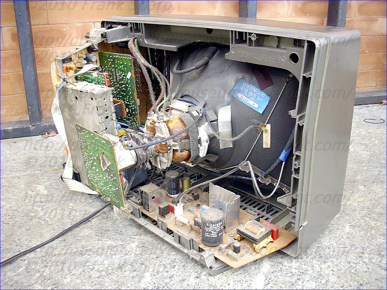
2. Circuit arrangement as set forth in claim 1, in which the picture signal comprises several color signals for the control of a corresponding number of beam currents for the display of a color picture in the picture tube and the control loop stores a part measuring signal or a part control signal derived therefrom for each color signal, characterized in that the change detection arrangement includes a change detector for each color signal which delivers a part change signal when the relevant stored signal has assumed a largely constant value, and the logic network does not release the control of the beam currents by the color signals outside the sampling intervals until the part change signals have been delivered by all change detectors.
3. Circuit arrangement as set forth in claim 1, including a comparator arrangement which compares the measuring signal with the reference signal and derives the control signal from this comparison, characterized in that the change detection arrangement detects a change in the control signal with respect to time and issues the change signal when the control signal has assumed a largely constant value.
4. Circuit arrangement as set forth in claims 1, 2, 3 including a control signal memory which contains at least one capacitor, characterized in that the change detection arrangement delivers the change signal when a charge-reversing current of the capacitor occuring during the starting up of the picture tube falls below a limit value.
5. Circuit arrangement as set forth in claim 2, including a comparator arrangement which compares the measuring signal with the reference signal and derives the control signal from this comparison, characterized in that the change detection arrangement detects a change in the control signal with respect to time and issues the change signal when the control signal has assumed a largely constant value.
The invention r
elates to a circuit arrangement for the control of at least one beam
current in a picture tube by a picture signal with a control loop which
in one sampling interval obtains a measuring signal from the value of
the beam current on the occurrence of a given reference level in the
picture signal, stores a control signal derived therefrom until the next
sampling interval and by this means adjusts the beam current to a value
preset by a reference signal, and with a trigger circuit which
suppresses auxiliary pulses used to generate the beam current after the
picture tube is turned on and issues a switching signal for the purpose
of closing the control loop during the sampling intervals and releasing
the control of the beam current by the picture signal after the
measuring signal has exceeded a threshold value. Such a circuit arrangement has been described in Valvo Technische Information 820705 with regard to the integrated color decoder circuit PHILIPS TDA3562A and is used in this as a so-called cut-off point control. In the known circuit arrangement, such a cut-off point control provides automatic compensation of the so-called cut-off point of the picture tube, i.e. it regulates the beam current in the picture tube in such a way that for a given reference level in the picture signal the beam current has a constant value despite tolerances and changes with time (aging, thermal modifications) in the picture tube and the circuit arrangement, thereby ensuring correct picture reproduction.
Such a blocking point control is particularly advantageous for the operation of a picture tube for the display of color pictures because in this case there are several beam currents for different color components of the color picture which have to be in a fixed ratio with one another. If this ratio changes, for example, as the result of manufacturing tolerances or ageing processes, distortions of the colors occur in the reproduction of the color picture. The beam currents, therefore, have to be very accurately balanced. The said cut-off point control prevents expensive adjustment and maintenance time which is otherwise necessary.

Conventional picutre tubes are constructed as cathode-ray tubes with hot cathodes which require a certain time after being turned on for the hot cathodes to heat up. Not until a final operating temperature has been reached do these hot cathodes emit the desired beam currents to the full extent, while gradually rising beam currents occur in the time interval when the hot cathodes are heating up. The instantaneous values of these beam currents depend on the instantaneous temperatures of the hot cathodes and on the accelerating voltages for the picture tube which build up simultaneously with the heating process and are undefined until the end of the heating time. After the picture tube is turned on, these values initially produce a highly distorted picture until the beam currents have attained their final value. These picture distortions after the picture tube is turned on are even further intensified by the fact that the cut-off point control is not yet adjusted to the beam currents which flow after the heating time is over.
For the purpose of suppressing distorted pictures during the heating time of the hot cathodes, the known circuit arrangement has a turn-on delay element
operating as a trigger circuit which, in essence, contains a bistable
flip-flop. When the picture tube and the circuit arrangement controlling
the beam currents flowing in it are turned on, the flip-flop is
switched into a first state in which it interrupts the supply of the
picture signal to the picture tube. Thus, during the heating time the
beam currents are suppressed, and the picture tube does not yet display
any picture. In sampling intervals which are provided subsequent to
flybacks of the cathode beam into an initial position on the changeover
from the display of one picture to the display of a subsequent picture
and even within the changeover, that is outside the display of pictures,
the picture tube is controlled for a short time in such a way that beam
currents occur when the hot cathodes are sufficiently heated up and an
accelerating voltage is resent. If these currents exceed a certain
threshold value, the flip-flop circuit switches into a second state and
releases the picture signal for the control of the beam currents and the
cut-off point control. It is found, however, that the picture displayed in the picture tube immediately after the switching over of the flip-flop is still not fault-free. Because, in fact, the beam currents are supported during the heating time of the hot cathodes, the cut-off point control cannot respond yet. This response of the cut-off point control takes place only after the beam currents are switched on, i.e. after the flip-flop is switched into the second state and therefore at a time in which the picture signal already controls the beam currents. In this way the response of the blocking point control makes its presence felt in the picture displayed.
With the known circuit arrangement the brightness of the picture gradually increases, during the response of the cut-off point control, from black to the final value.
This slow increase in the picture brightness after the tube is turned on is disturbing to the eyes of the viewer not only in the case of the black-and-white picture tubes with one hot cathode, but especially so in the case of colour picture tubes which usually have three hot cathodes. With a color picture tube, color purity errors can also
occur in addition to the change in the picture brightness if, as a
result of different speeds of response of the cut-off point control for
the three beam currents, there are found to be intermittent variations
from the interrelation between the beam currents required for a correct
picture reproduction.SUMMARY OF THE INVENTION
The aim of the invention is to create a circuit arrangement which suppresses the above-described disturbances of brightness and color of the displayed picture when the picture tube is being started.
The invention achieves this aim in that a circuit arrangement of the type mentioned in the preamble contains a change detection arrangement which emits a change signal when the stored signal has assumed an essentially constant value, and a logic network which does not release the control of the beam current by the picture signal until the change signal has also been emitted after the switching signal.
In the circuit
arrangement according to the invention, therefore, the display of the
picture is suppressed after the picture tube is turned on until the
cut-off point control has responded. If the picture signal then starts
to control the beam current, a perfect picture is displayed immediately.
In this way, all the disturbances of the picture which affect the
viewer's pleasure are suppressed. The circuit arrangement of the
invention is of simple design and can be combined on one semiconductor
wafer with the existing picture signal processing circuits and also, for
example, with the known circuit arrangement for cut-off point control.
Such an integrated circuit arrangement not only requires very little
space on the semiconductor wafer, but also needs no additional external
leads. Thus the circuit arrangement of the invention can be arranged,
for example, in an integrated circuit which has precisely the same
external connections as known integrated circuits. This means that an
integrated circuit containing the circuit arrangement of the invention
can be directly incorporated in existing equipment without the need for
additional measures. In one embodiment of the said circuit arrangement, in which the picture signal contains several color signals for the control of a corresponding number of beam currents for representing a color picture in the picture tube and, for each color signal, the control loop stores a part measuring signal or a part control signal derived from it, the change detection arrangement contains a change detector for each color signal which emits a part change signal when the relevant stored signal has assumed an essentially constant value, and the logic network does not release the control of the beam currents by the color signals outside the sampling intervals until the part change signals have been emitted from all change detectors.
In principle, therefore, such a circuit arrangement has three cut-off point controls for the three beam currents controlled by the individual color signals. To reduce the cost of the circuitry, the measuring stage is common to all the cut-off point controls, as in the known circuit arrangement. All three beam currents are then measured successively by this measuring stage. In this way, a part measuring signal or a part control signal derived from it is obtained for each beam current and is stored sesparately according to which of the beam currents it belongs. Changes in the part measuring signal or part control signal are detected for each beam current by one of the change detectors each time. Each of these change detectors issues a part change signal to the logic network. The latter does not release the control of the beam currents by the picture signal outside the sampling intervals until all the part change signals indicate that the part measuring signal or the part control signal, as the case may be, remains constant. This ensures that the cut-off point controls for the beam currents of all color signals have responded when the picture appears in the picture tube.
In a further embodiment of the circuit arrangement according to the invention with a comparator arrangement which compares the measuring signal with the reference signal and derives the control signal from this comparison, the change detection arrangement detects a change in the control signal with respect to time and issues the change signal when the control signal has assumed an essentially constant value. In the case of the representation of a color signal the comparator arrangement derives several part control signals, whose changes with time are detected by the change detectors, from a corresponding comparison of the part measuring signals with the reference signal. In this embodiment of the circuit arrangement of the invention, preference is given to storage of only the control signal or the part control signals for the purpose of controlling the beam currents.
In another embodiment of the circuit arrangement of the invention which includes a control signal memory which contains at least one capacitor in which a charge or voltage corresponding to the control signal is stored, the change detection arrangement issues the change signal when a charge-reversing current of the capacitor occurring during the turning on of the picture tube has fallen below a limit value and has thus at least largely decayed. Such a detection of the steady state of the cut-off point control is independent of the actual magnitude of the control signal and therefore independent of, for example, the level of the picture tube cut-off voltage, circuit tolerances or ageing processes in the circuit arrangement or the picture tube.
Detection of whether or not the charge-reversing current exceeds the limit value is performed preferentially by a current detector which is designed with a current mirror system which is arranged in a supply line to a capacitor acting as a control signal store. A current mirror arrangement of this kind supplies a current which coincides very precisely with the charging current of the capacitor. This current is then compared, preferably in a further device contained in the change detection arrangement, with a current representing a limit value or, after conversion into a voltage, with a voltage representing the limit value. The change signal is obtained from the result of this comparison.
On the other hand, digital memories may also be used as control signal memories, especially when the picture signal is supplied as a digital signal and the blocking point control is constructed as a digital control loop. In such a case, the comparator arrangement, the change detection arrangement and the trigger circuit are also designed as digital circuits. Then, the change detection arrangement advantageously forms the difference of the signals stored in the control signal memory in two successive sampling intervals and compares this with the limit value formed by a digital value. If the difference falls short of the limit value, the change signal is issued.
BRIEF DESCRIPTION OF THE DRAWINGS
An embodiment of the invention is described in greater detail below with the aid of the drawings in which:
FIG. 1 shows a block circuit diagram of the embodiment,
FIG. 2 shows a somewhat more detailed block circuit diagram of the embodiment,
FIG. 3 shows time-dependency diagrams of some signals occurring in the circuit diagram shown in FIG. 2, and
FIG. 4 shows a somewhat moredetailed block circuit diagram of a part of the circuit diagram shown in FIG. 2.
 DETAILED DESCRIPTION OF THE INVENTION
FIG. 1 shows a block circuit diagram of a circuit arrangement to which a picture signal is fed via a first input 1 of a combinatorial stage 2. From the output 3 of the combinatorial stage 2 the picture signal is fed to the picture signal input of a controllable amplifier 5 which at an output 6 issues a current controlled by the picture signal. This current is fed via a measuring stage 7 to a hot cathode 8 in a picture tube 9 and forms therein a beam current of a cathode ray by means of which a picture defined by the picture signal is displayed on a fluorescent screen of the picture tube 9.
The measuring stage 7 measures the current fed to the hot cathode 8, i.e. the the beam current in the picture tube 9, and at a measuring signal output 10, issues a measuring signal corresponding to the magnitude of this current. This is fed to a measuring signal input 11 of a comparator arrangement 12 to which a reference signal is supplied at a reference signal input 13. In a preferably periodically recurring sampling interval during the occurrence of a given reference level in the picture signal, the comparator arrangement 12 forms a control signal from the value of the measuring signal fed to the measuring signal input 11 at this time, on the one hand, and the reference signal, on the other, by means of substraction and delivers this at a control signal output 14. From there the control signal is fed to an input 15 of a control signal memory 16 and is stored in the latter. The control signal is fed via an output 17 of the control signal memory 16 to a second input 18 of combinatorial stage 2 in which it is combined with the picture signal, e.g. added to it.
The combinatorial stage 2, the controllable amplifier 5, the measuring stage 7, the comparator arrangement 12 and the control signal memory 16 form a control loop with which the beam current is guided towards the reference signal in the sampling interval during the occurrence of the reference level in the picture signal. For the reference level, use is made in particular of a black level or a level with small, fixed distance from the black level, i.e. a value in the picture signal w
hich produces a black or almost back picture area in the
displayed picture in the picture tube. In this case the control loop,
as described, forms a cut-off point control for the picture tube. If the
reference level is away from the black level, the control loop is also
designated as quasi-cut-off-point control. The circuit arrangement as shown in FIG. 1 also has a trigger circuit 19 to which the measuring signal from the measuring signal output 10 of measuring stage 7 is fed at a measuring signal input 20. When the circuit arrangement and therefore the picture tube are turned on, the trigger circuit 19 is set in a first state in which by means of a first connection 21 it blocks the comparator arrangement 12 in such a way that the latter delivers no control signal or a control signal with the value zero at its control signal output 14. This prevents the control signal memory 16 from storing undefined values for the control signal at the moment of turning on or immediately thereafter.
The circuit arrangement shown in FIG. 1 also has a logic network 22 which is connected via a second connection 23, by means of which a switching signal is supplied, with the trigger circuit 10 and via a third connection 24 with the controllable amplifier 5. Like the trigger circuit 19, the logic network 22 also finds itself controlled, when the circuit arrangement is being turned on, by the switching signal in a first stage in which by way of the third connection 24 it blocks the controllable amplifier 5 with a blocking signal in such a way that no beam currents controlled by the picture signal can yet flow in the picture tube 9. Thus the picture tube 9 is blanked; no picture is displayed yet.
When picture tube 9 is turned on, the hot cathode 8 is still cold so that no beam current can flow anyhow. The hot cathode 8 is then heated up and, after a certain time, begins gradually to emit electrons as the result of which a cathode ray and therefore a beam current can form. However, during the heating up of the hot cathode 8, and because the cut-off point control has not yet responded, this would be undefined and is therefore suppressed by the controllable amplifier 5. Only in time intervals which are provided immediately subsequent to flybacks of the cathode rays into an initial position at the changeover from the display of one image to that of a subsequent image, but even before the start of the display of the subsequent image, the controllable amplifier 5 delivers a voltage in the form of an auxiliary pulse for a short time at its output 6, and when the hot cathode 8 in the picture tube 9 is heated up sufficiently, this voltage produces a beam current. The time interval for the delivery of this voltage is selected in such a way that a cathode ray produced by its does not produce a visible image in the picture tube 9, and coincides for example with the sampling interval.
The measuring stage 7 measures the short-time cathode current produced in the manner described and, at its measuring signal output 10, delivers a corresponding measuring signal which is passed via measuring signal output 20 to the trigger circuit 19. If the measuring signal exceeds a definite preset threshold value, the trigger circuit 19 is switched into a second state in which it releases the comparator arrangement 12 via the first connection 12 and, by means of the second connection 23, uses the switching signal to also bring the logic network 22 into a second state. The comparator arrangement 12 now evaluates the measuring signal supplied to it via the measuring signal input 11, i.e. it forms the control signal as the difference between the measuring signal and the reference signal supplied via the reference signal input 13. The control signal is transferred via the control signal output 14 and the input 15 into the control signal memory 16. It is subsequently fed via the output 17 of the control signal memory 16 to the second input 18 of the combinatorial stage 2 and is there combined with the picture signal at the first input 1, e.g. is superimposed on it by addition. This superimposed picture signal is fed to the picture signal input 4 of the controllable amplifier 5 via the output 3 of the combinatorial stage 2.
In the
second state of the logic network 22 the controllable amplifier 5 is
switched via the third connection 24 by the blocking signal in such a
way that the picture signal controls the beam currents only during the
sampling intervals and that, for the rest, no image appears yet in the
picture tube. The cut-off point control now gebins to respond, i.e. the
value of the control signal is changed by the control loop comprising
the combinatorial stage 2, the controllable amplifier 5, the measuring
stage 7, the comparator arrangement 12 and the control signal memory 16
until such time as the beam current in the picture tube 9 at the
blocking point or at a fixed level with respect to it is adjusted to a
value preset by the reference signal. For this purpose the sampling
interval, in which the picture signal controls the beam current via the
controllable amplifier 5 is selected in such a way that within it the
picture signal just assumes a value corresponding to the cut-off point
or to a fixed level with respect to it.During the response of the cut-off point control the control signal fed to the control signal memory 16 changes continuously. Between the control signal output 14 of the comparator arrangement 12 and the input 15 of the control signal memory 16 is inserted a changed detection arrangement 25 which detects the variations of the control signal. When the cut-off point control has responded, i.e. the control signal has assumed a constant value, the change detection arrangement 25 delivers a change signal at an output 26 which indicates that the steady stage of the cut-off point control is achieved and the said signal is fed to a change signal input 27 of the logic network 22. The logic network then switches into a third state in which via the third connection 24 it enables the controllable amplifier 5 in such a way that the beam currents are now controlled without restriction by the picture signal. Thus a correctly represented picture appears in the picture tube 9.
A shadow-like representation of individual constituents of the circuit arrangement in FIG. 1 is used to indicate a modification by which this circuit arrangement is equipped for the representation of color pictures in the picture tube 9. For example, three color signals are fed in this case as the picture signal via the input 1 to the combinatorial stage 2. Accordingly, the input 1 is shown in triplicate, and the combinatorial stage 2 has a logic element, e.g. an adder, for example of these color signals. The controllable amplifier 5 now has three amplifier stages, one for each of the color signals, and the picture tube now contains three hot cathodes 8 instead of one so that three independent cathode rays are available for the three color signals.
However, to simplify the circuit
arrangement and to save on components, only one measuring stage 7 is
provided which measures all three beam currents successively. Also, the
comparator arrangement 12 forms part control signals from the
successively arriving part measuring signals for the individual beam
currents with the reference signal, and these part control signals are
allocated to the individual color signals and passed on to three storage
units which are contained in the control signal memory 16. From there,
the part control signals are sent via the second input 18 of the
combinatorial stage 2 to the assigned logic elements. The circuit arrangement thus forms three independently acting control loops for the cut-off point control of the individual color signals, in which case only the measuring stage 7 and to some extent at least the comparator arrangement 12 are common to these control loops.
The change detection arrangement 25 now has three change detectors each of which detects the changes with time of the part control signals relating to a color signal. Then via the output 26 each of these change detectors delivers a part change signal to the change signal input 27 of the logic network 22. These part change signals occur independently of one another when the relevent control loop has responded. The logic network 22 evaluates all three part change signals and does not switch into its third stage until all part change signals indicate a steady state of the control loops. Only then, in fact, is it ensured that all the color signals from the beam currents controlled by them are correctly reproduced in the picture tube, and thus no distortions of the displayed image, especially no color purity errors, occur. The color picture displayed then immediately has the correct brightness and color on its appearance when the picture tube is turned on.

FIG. 2 shows a somewhat more detailed block circuit diagram of an embodiment of a circuit arrangement equipped for the processing of a picture signal containing three colour signals. Three color signals for the representation of the colors red, green and blue are fed to this circuit arrangement via three input terminals 101, 102, 103. A red color signal is fed via the first input terminal 101 to a first adder 201, a green colour signal is fed via the second input terminal to a second adder 202, and a blue colour signal is fed via the third input terminal 103 to a third adder 203. From outputs 301, 302 and 303 of the adders 201, 202, 203 the color signals are fed to amplifier stages 501, 502 and 503 respectively. Each of the amplifier stages contains a switchable amplifier 511, 512 and 513, an output amplifier 521, 522 and 523 as well as a measuring transistor 531, 532 and 533 respectively. The emitters of these measuring transistors 531, 532, 533 are each connected to a hot cathode 801, 802, 803 of the picture tube 9 and deliver the cathode currents, whereas the collectors of measuring transistors 521, 532, 533 are connected to one another and to a first terminal 701 of a measuring resistor 702 the second terminal of which 703 is connected to earth. Th
e
current gain of the measuring transistors 531, 532 and 533 is so great
that their collector currents coincide almost with the cathode currents.
By measuring the voltage drop produced by the cathode currents at the
measuring resistor 802 it is then possible to measure the cathode
currents and therefore the beam currents in the picture tube 9 with
great accuracy. The falling voltage at the measuring resistor 702 is fed as a measuring signal to an input 121 of a buffer amplifier 120 with a gain factor of one, at the output 122 of which the unchanged measuring signal is therefore available at low impedance. From there it is fed to a first terminal 131 of a reference voltage source 130 which is connected with its second terminal 132 to inverting inputs 111, 112 and 113 of three differential amplifiers 123, 124, 125 respectively. The differential amplifiers 123, 124, 125 also each have a non-inverting input 114, 115, and 116 respectively. These are connected to each other at a junction 117, to earth via a leakage current storage capacitor 126 and to the output 122 of the buffer amplifier 120 via decoupling resistor 118 and a leakage current sampling switch 119. In addition, the input 121 of the buffer amplifier 120 can be connected to earth via a short-circuiting switch 127.

The operation of the comparator arrangement 12 which consists mainly of the buffer amplifier 120, the reference voltage source 130 and differential amplifiers 123, 124, 125 will be explained below with the aid of the pulse diagrams in FIG. 3. FIG. 3a shows a horizontal blanking signal for a television signal which, as the picture signal, controls the beam currents in the picture tube 9. In this diagram, H represents horizontal blanking pulses which follow one another in the picture signal at the time interval of one line duration and by means of which the beam currents are switched off during line flyback between the display of the individual picture lines in the picture tube. FIG. 3b shows a vertical blanking pulse V by means of which the beam currents are switched off during the change ober from the display of one picture to the display of the next picture. FIG. 3c shows a measuring signal control pulse VH which is formed from a vertical blanking pulse lengthened by three line duration.
The short-circuiting switch 127 is now controlled in such a way that it is non-conducting only throughout the duration of the measuring signal control pulse VH and during the remaining time short-circuits the input 121 of the buffer amplifier 120 to earth. This means that a measuring signal only reaches the comparator arrangement 12 during frame change so that the parts of the picture signal which control the beam currents producing the picture in the picture tube exert no influence on comparator arrangement 12 and therefore on the blocking point control.
Throughout the duration
of the measuring signal control pulse VH, the measuring signal from
output 122, reduced by a reference voltage issued by the reference
voltage source 130 between its first 131 and its second terminal 132, is
present at the inverting inputs 111, 112, 113 of differential
amplifiers 123, 124, 125. If the differential amplifiers 123, 124, 125
were not present, this difference would be fed directly as part control
signals to the control signal storage capacitors 161, 162, 162. The
differential amplifiers 123, 124, 125 amplify the difference and thus
form the control amplifiers of the control loops. The part control signal is fed from output 141 of differential amplifier 123 by the first control signal sampling switch 154 to the first terminal 151 of the first control signal storage capacitor 161 during the period of a storage pulse L1 and is stored in the said capacitor. Similarly, the part control signal from output 143 of differential amplifier 125 is fed to the third control signal storage capacitor 163 during the period of a storage pulse L2 and the part control signal from output 142 of differential amplifier 124 is fed to the second control signal storage capacitor 162 during a storage pulse L3. The storage pulses L1, L2 and L3 are illustrated in FIGS. 3d, e and f. They lie in sequence in one of the three line periods by which the measuring signal control pulse VH is longer than the vertical blan
king pulse V. These three line periods form
the sampling interval for the measuring signal or the part measuring
signals, as the case may be. During the remaining periods the outputs,
141, 152, 143 of the differential amplifiers 123, 124, 125 are isolated
from the control signal storage capacitors 161, 162, 163 so that no
interference can be transmitted from there and any distortion of the
stored part control signals caused thereby is eliminated. For the
duration of storage pulses L1, L2 and L3 the color signals at the input
terminals 101, 102, 103 are at their reference level i.e. in the present
embodiment at a level, corresponding to the blocking point or at a
fixed level with respect to it so that the control loops can adjust to
this level.The switchable amplifiers 511, 512, and 513 each receive at each input 241, 242, 243 a blanking signal BL1, BL2, BL3 respectively, the curves of which are shown in FIGS. 3g, h, i. These blanking signals interrupt the supply of the color signals during line flybacks and frame change, i.e. during the period of the measuring signal control pulse VH, and thus the beam currents in these time intervals are switched off. Naturally, the red color signal is let through during the first line period after the end of the vertical blanking pulse V, the blue color signal during the second line period after the end of the vertical blanking pulse V and the green color signal during the third line period after the end of the vertical blanking pulse V by the switchable amplifiers 511, 512, 513 respectively so that they can control the beam currents. Blanking signals BL1, BL2 and BL3 also provide for interruptions in the frame change blanking pulse, which corresponds to the measuring signal control pulse, in the corresponding time intervals. In these time intervals the beam currents are measured and part control signals are determined from the part measuring signals and stored in the control signal storage capacitors 161, 162, 163.
The circuit arrangement shown in FIG. 2 further contains a trigger circuit 19 to which a supply voltage is fed via a supply terminal 190. Via a reset input 191 a voltage is also
supplied to
the trigger circuit 19 from a third terminal 133 of the reference
voltage source 130. When the circuit arrangement is turned on, this
voltage is designed so as to be delayed with respect to the supply
voltage so that when the circuit arrangement is brought into operation
the interplay of the two voltages produces a switch-on reset signal such
that a low-value voltage pulse occurs at the reset input 191 during
turn on, which means that the trigger circuit 19 is set in its first
state. The reset input 191 can also be connected to another circuit of
any configuration which generates a switch-on reset signal when the
picture tube is turned on. The trigger circuit 19 is further connected via a second connection 23 to a logic network 22 which, when the circuit arrangement is turned on, is also set into a first state via the second connection 23. In this first state the logic network 22 delivers a blocking signal at a blocking output 240 which is fed to the three switchable amplifiers 511, 512, 513. By this means the supply of the color signals to the output amplifiers 521, 522, 523 is interrupted completely so that no beam currents can be generated by these. No picture is therefore displayed.
An insertion signal EL which
extends over the three line periods by which the measuring signal
control pulse VH is longer than the vertical blanking pulse V, i.e. over
the sampling interval, is also fed via a line 233 to the trigger
circuit 19 and the logic network 22. As long as the trigger circuit 19
is in its first state, this insertion pulse EL is issued via a control
output 192 from the trigger circuit 19 and fed to the pulse generator
244. During the period of the insertion pulse EL this generator produces
a voltage pulse of a definite magnitude and passes this to output
amplfiiers 521, 522, 523 as an auxiliary pulse via switching diodes 245,
246, 247. By this means the beam currents are switched on for a short
time so as to receive a measuring signal despite the disconnected color
signals as soon as at least one of the hot cathodes 801, 802, 803
delivers a beam current. In its first state the trigger circuit 19 also delivers a signal via a control line 211, and this signal is used to switch the outputs 141, 142, 143 of the differential amplifiers 123, 124, 125 to earth potential or practically to earth potential. This suppresses effects of voltages at the inputs 111 to 116 of the differential amplifiers 123, 124, 125, especially effects of the reference voltage source 130 which may in some cases initiate incorrect charging of the control signal storage capacitors 161, 162, 163.
The measuring signal produced by means of the pulse generator 244 at the input 121 of the buffer amplifier 120 is also fed to the trigger circuit 19 via a measuring signal input 20. If it exceeds a preset threshold value, the trigger circuit 19 switched into its second state. The logic network 22 is then also switched into its second state via the second connection 23. The differential amplifiers 123, 124, 125, too, are triggered by th
e signal along the control line 211 into issuing a
control signal defined by the difference in the voltages at its inputs
111 to 116. The pulse generator 244 is blocked by the control output
192. The blocking signal issued from the blocking output 240 of the
logic network 22 now turns on the switchable amplifiers 511, 512, 513 in
the time intervals defined by the storage pulses L1, L2, L3 in such a
way that in these time intervals the color signals can produce beam
currents to form a measuring signal by which the control loops respond.
However, the display of the picture is still suppressed. The control
signal storage capacitors 161, 162, 163 are charged up in this process.
In the leads to the first terminals 151, 152, 153 there are change
detectors 251, 252, 253 which detect the changes of the charging
currents of the control signal storage capacitors 161, 162, 163 and at
their outputs 261, 262, 263 in each case deliver a part change signal
when the charging current of the control signal storage capacitor in
question has decayed and thus the relevant control loop has responded.
The part change signals are fed to three terminals 271, 272, 273 of the
change signal input 27 of the logic network 22. When part change signals are present from all change detectors 251, 252, 253, when therefore all control loops have responded, the logic network 22 switches from its second to its third state. The blocking signal from the blocking output 240 is now completely disconnected such that the switchable amplifiers 511, 512, 513 are now switched only by the blanking signals BL1, BL2, BL3. The colour signals are then switched through to the output amplifiers 521, 522, 523 and the picture is displayed in the picture tube.

FIG. 4 shows an embodiment for a trigger circuit 19 and a logic network 22 of the circuit arrangements as shown in FIGS. 1 or 2. The trigger circuit 19 contains a flip-flop circuit formed from two NAND-gates 194, 195 to which the switch-on reset signal, by which the trigger circuit 19 is returned to its first stage, is fed via the reset input 191. All the elements of the circuit arrangement in FIG. 4 are shown in positive logic. Thus, a short-time low voltage at the reset input 191 immediately after the circuit arrangement is started up is used to set the flip-flop circuit 194, 195 in such a way that a high voltage occurs at the output of the second NAND gate 194 and a low voltage at the output of the second NAND gate 195. The low voltage at the output of the second NAND gate 195 blocks differential amplifiers 123, 124, 125 via the control line 211 in the manner described.
The insertion pulse EL is fed via the line 233 to the trigger circuit 19, is combined via an AND gate 196 with the signal from the output of the first NAND gate 194 and is delivered at the control output 192 for the purpose of controlling the pulse generator 244.
The signals from the outputs of the NAND-gates 194, 195 are fed via a first line 231 and a second line 232 of the second connection 23 as a switching signal to the logic network 22. The first line 231 is connected to reset inputs R of three part change signal memories 221, 222, 223 in the form of bistable flip-flop circuits which when the circuit arrangement is started up are reset via the first line 231 in such a way that they carry a low voltage at their outputs Q. The second line 232 of the second connection 23 leads via three AND gates 224, 225, 226 to setting inputs S of the three part change signal memories 221, 222, 223. By means of the AND gates 224, 225, 226 the signal on the second line 232 of the second connection 23 is combined each time with one of the part change signals supplied via the terminals 271, 272, 273. The signals from the outputs Q of the part change signal memories 221, 222, 223 are combined by means of a collecting gate 227 in the form of an NAND gate and are held ready at its output 228.
The measuring signal is fed to the trigger
circuit 19 via the measuring signal input 20 and passed to a first input
197 of a threshold detector 198 to which at a second input a threshold
value, in the form of a threshold voltage for example, produced by a
threshold generator 199 is also supplied. When the voltage at the first
input 197 of the threshold detector 198 is smaller than the voltage
delivered by the threshold generator 199, the threshold detector 198
delivers a high voltage at its output 200. When, on the other hand, the
voltage at the first input 197 is greater than the voltage of the
threshold generator 199, the voltage at the output 200 jumps to a low
value. This voltage is supplied as the setting signal of the flip-flop
circuit 194, 195, reverses the latter and thereby switches the trigger
circuit 19 into its second state when the voltage at the first input 197
exceeds the voltage of the threshold generator 199. After the switching over of the flip-flop circuit 194, 195 corresponding to the setting of the trigger circuit 19 into the second state, appropriately modified signals are supplied via the control line 211 and the output 192 for the purpose of controlling the pulse generator 244 and the differential amplifiers 123, 124, 125. Modified voltages also appear on the lines 231, 232 of the second connection 23, and these voltages release the part change signal memories 221, 222, 223 such that they can each be set when the part change signals reach the terminals 271, 272, 273.
The signal at the output 228 of the collecting gate 227 changes its state when the last of the three part change signals has also arrived and has set the last of the three part change signal memories. The signal is then combined via a gate arrangement 229 of two NAND gates and one AND gate with the insertion pulse EL of line 223 and with the signal on the second line 232 of the second connection 23 or from the output Q of the further flip-flop circuit 234 to the blocking signal delivered at the blocking output 24 which is fed to the switchable amplifiers 511, 512, 513.
The circuit arrangement described is designed in such a way that the trigger circuit 19 remains in its second state and logic network 22 remains in its third state even if charging currents reappear at the difference signal storage cpacitors 161, 162, 163 due to disturbances during the operation of the circuit arrangement. The cutoff point control then makes readjustments without the displayed picture being disturbed.
In the circuit arrangement shown in F
IG. 2, the green
color signal can also be let through during the second line period after
the end of the vertical blanking pulse V and the blue color signal
during the third line period after the end of the vertical blanking
pulse V by the switchable amplifiers 511, 512, 513 for the purpose of
controlling the beam currents. The storage pulses L2 and L3 at the
control signal sampling switches 155 and 156 and the second and third
blanking signals BL2 and BL3 at the blanking inputs 242 and 243 are then
to be interchanged. The resulting insertion signals A2 and A3 as shown
in FIGS. 3m and n are also interchanged then accordingly. In FIG. 2 a dashed line is used to indicate which components of the circuit arrangement can be combined advantageously to form an integrated circuit. The first terminals 151, 152, 153 of the difference signal storage capacitors 161, 162, 163, one terminal 128 of leakage current storage capacitor 126, three terminals 524, 525, 526 in the leads to the output amplifiers 521, 522, 523 as well as a line connection 704 between the first terminal 701 of the measuring resistor 702 and the input 121 of the buffer amplifier 120 will then form the connecting contacts of this integrated circuit.


ABLENKUNG BAUSTEIN 29504-007...
TDA2595 (Synch) (PHILIPS)
TDA2655 (Frame) (PHILIPS)
TDA2595 Horizontal combination
GENERAL DESCRIPTION
The TDA2595 is a monolithic integrated circuit intended for use in colour television receivers.
Features
· Positive video input; capacitively coupled (source impedance < 200 W)
· Adaptive sync separator; slicing level at 50% of sync amplitude
· Internal
vertical pulse separator with double slope integrator· Output stage for vertical sync pulse or composite sync depending on the load; both are switched off at muting
· j1 phase control between horizontal sync and oscillator
· Coincidence detector j3 for automatic time-constant switching; overruled by the VCR switch
· Time-constant switch between two external time-constants or loop-gain; both controlled by the coincidence detector j3
· j1 gating pulse controlled by coincidence detector j3
· Mute circuit depending on TV transmitter identification
· j2 phase control between line flyback and oscillator; the slicing levels for j2 control and horizontal blanking can be set
separately
· Burst keying and horizontal blanking pulse generation, in combination with clamping of the vertical blanking pulse
(three-level sandcastle)
· Horizontal drive output with constant duty cycle inhibited by the protection circuit or the supply voltage sensor
· Detector for too low supply voltage
· Protection circuit for switching off the horizontal drive output continuously if the input voltage is below 4 V or higher
than 8 V
· Line flyback control causing the horizontal blanking level at the sandcastle output continuously in case of a missing
flyback pulse
· Spot-suppressor controlled by the line flyback control.
TDA2655B VERTICAL DEFLECTION CIRCUIT

GENERAL DESCRIPTION
The TDA2655B is a monolithic integrated circuit for vertical deflection in colour television receivers
with 90° picture tubes.
Features:
- Synchroniz
ation circuit- Vertical oscillator; 50/60 Hz switch
- Sawtooth generator with buffer stage
- Preamplifier with fedout inputs
- Output stage with termal and shortcircuit protection
- Flyback generator
- Blanking pulse generator with guard circuit
- Voltage stabilizer
- Frequency detector with memory and storage.
CRT TV EHT VOLTAGE MULTIPLIER - KASKADE COCKCROFT-WALTON CASCADE CIRCUIT FOR VOLTAGE MULTIPLICATION:

A Cockcroft-Walton cascade circuit comprises an input voltage source and a pumping and storage circuit with a series array of capacitors with pumping and storage portions of the circuit being interconnected by silicon rectifiers, constructed and arranged so that at least the capacitor nearest the voltage source, and preferably one or more of the next adjacent capacitors in the series array, have lower tendency to internally discharge than the capacitors in the array more remote from the voltage source.
1. An improved voltage multiplying circuit comprising,
2. An improved voltage multiplying circuit in accordance with claim 1 wherein said first pumping capacitor is a self-healing impregnated capacitor which is impregnated with a high voltage impregnant.
3. An improved voltage multiplying circuit in accordance with claim 1 wherein said first pumping capacitor comprises a foil capacitor.
Description:
BACKGROUND OF THE INVENTION
The invention relates in general to Cockcroft-Walton cascade circuits for voltage multiplication and more particularly to such circuits with a pumping circuit and a storage circuit composed of capacitors connected in series, said pumping circuits and storage circuit being linked with one another by a rectifier circuit whose rectifiers are preferably silicon rectifiers, especially for a switching arrangement sensitive to internal discharges of capacitors, and more especially a switching arrangement containing transistors, and especially an image tube switching arrangement.
Voltage multiplication cascades composed of capacitors and rectifiers are used to produce high D.C. voltages from sinusoidal or pulsed alternating voltages. All known voltage multiplication cascades and voltage multipliers are designed to be capacitance-symmetrical, i.e., all capacitors used have the same capacitance. If U for example is the maximum value of an applied alternating voltage, the input capacitor connected directly to the alternating voltage source is charged to a D.C. voltage with a value U, while all other capacitors are charged to the value of 2U. Therefore, a total voltage can be obtained from the series-connected capacitors of a capacitor array.
In voltage multipliers, internal resistance is highly significant. In order to obtain high load currents on the D.C. side, the emphasis in the prior art has been on constructing voltage multipliers with internal resistances that are as low as possible.
Internal resistance of voltage multipliers can be reduced by increasing the capacitances of the individual capacitors by equal amounts. However, the critical significance of size of the assembly in the practical application of a voltage multiplier, limits the extent to which capacitance of the individual capacitors can be increased as a practical matter.
In television sets, especially color television sets, voltage multiplication cascades are required whose internal resistance is generally 400 to 500 kOhms. Thus far, it has been possible to achieve this low internal resistance with small dimensions only by using silicon diodes as rectifiers and metallized film capacitors as the capacitors.
When silicon rectifiers are used to achieve low internal resistance, their low forward resistance produces high peak currents and therefore leads to problems involving the pulse resistance of the capacitors. Metallized film capacitors are used because of space requirements, i.e., in order to ensure that the assembly will have the smallest possible dimensions, and also for cost reasons. These film capacitors have a self-healing effect, in which the damage caused to the capacitor by partial evaporation of the metal coating around the point of puncture (pinhole), which develops as a result of internal spark-overs, is cured again. This selfhealing effect is highly desirable as far as the capacitors themselves are concerned, but is not without its disadvantages as far as the other cirucit components are concerned, especially the silicon rectifiers, the image tubes, and the components which conduct the image tube voltage.
It is therefore an important object of the invention to improve voltage multiplication cascades of the type described above.
It is a further object of the invention to keep the size of the entire assembly small and the internal resistance low.
It is a further object of the invention to increase pulse resistance of the entire circuit.
It is a further object of the invention to avoid the above-described disadvantageous effects on adjacent elements.
It is a further object of the invention to achieve multiples of the foregoing objects and preferably all of them consistent with each other.
SUMMARY OF THE INVENTION
In accordance with the invention, the foregoing objects are met by making at least one of the capacitors in the pumping circuit, preferably including the one which is adjacent to the input voltage source, one which is less prone to internal discharges than any of the individual capacitors in the storage circuit.
The Cockcroft-Walton cascade circuit is not provided with identical capacitors. Instead, the individual capacitors are arranged according to their loads and designed in such a way that a higher pulse resistance is attained only in certain capacitors. It can be shown that the load produced by the voltage in all the capacitors in the multiplication circuit is approximately the same. But the pulse currents of the capacitors as well as their forward flow angles are different. In particular, the capacitors of the pumping circuit are subjected to very high loads in a pulsed mode. In the voltage multiplication cascade according to the invention, these capacitors are arranged so that they exhibit fewer internal discharges than the capacitors in the storage circuit.
The external dimensions of the entire assembly would be unacceptably large if one constructed the entire switching arrangement using such capacitors.
The voltage multiplication cascade according to the invention also makes it possible to construct a reliably operating

arrangement which has no tendency toward spark-overs, consistent with satisfactory internal resistance of the voltage multiplication cascade and small dimensions of the entire assembly. This avoids the above cited disadvantages with respect to the particularly sensitive components in the rest of the circuit and makes it possible to design voltage multiplication cascades with silicon rectifiers, which are characterized by long lifetimes. Hence, a voltage multiplication cascade has been developed particularly for image tube circuits in television sets, especially color television sets, and this cascade satisfies the highest requirements in addition to having an average lifetime which in every case is greater than that of the television set.
A further aspect of the invention is that at least one of the capacitors that are less prone to internal discharges is a capacitor which is impregnated with a high-voltage impregnating substance, especially a high-voltage oil such as polybutene or silicone oil, or mixtures thereof. In contrast to capacitors made of metallized film which have not been impregnated, this allows the discharge frequency due to internal discharges or spark-overs to be reduced by a factor of 10 to 100.
According to a further important aspect of the invention, at least one of the capacitors that are less prone to internal discharges is either a foil capacitor or a self-healing capacitor. In addition, the capacitor in the pumping circuit which is adjacent to the voltage source input can be a foil capacitor which has been impregnated in the manner described above, while the next capacitor in the pumping circuit is a self-healing capacitor impregnated in the same fashion.
Other objects, features and advantages of the invention will be apparent from the following detailed description of preferred embodiments, taken in connection with the accompanying drawing, the single FIGURE of which:
BRIEF DESCRIPTION OF THE DRAWING
is a schematic diagram of a circuit made according to a preferred embodiment of the invention.
DETAILED DESCRIPTION OF PREFERRED EMBODIMENTS
The voltage multiplier comprises capacitors C1 to C5 and rectifiers D1 to D5 connected in a cascade. An alternating voltage source UE is connected to terminals 1 and 2, said voltage source supplying for example a pulsed alternating voltage. Capacitors C1 and C2 form the pumping circuit while capacitors C3, C4 and C5 form the storage circuit.
In the steady state, capacitor C1 is charged to the maximum value of the alternating voltage UE as are the other capacitors C2 to C5. The desired high D.C. voltage UA is picked off at terminals 3 and 4, said D.C. voltage being composed of the D.C. voltages from capacitors C3 to C5. Terminal 3 and terminal 2 are connected to one pole of the alternating voltage source UE feeding the circuit, which can be at ground potential. In the circuit described here, a D.C. voltage UA can be picked off whose voltage value is approximately 3 times the maximum value of the pulsed alternating voltage UE. By using more than five capacitors, a correspondingly higher D.C. voltage can be obtained.

The individual capacitors are discharged by disconnecting D.C. voltage UA. However, they are constantly being recharged by the electrical energy supplied by the alternating voltage source UE, so that the voltage multiplier can be continuously charged on the output side.
According to the invention, in this preferred embodiment, capacitor C1 and/or C2 in the pumping circuit are designed so that they have a lower tendency toward internal discharges than any of the individual capacitors C3, C4 and C5 in the storage circuit.
It is evident that those skilled in the art, once given the benefit of the foregoing disclosure, may now make numerous other uses and modifications of, and departures from the specific embodiments described herein without departing from the inventive concepts. Consequently, the invention is to be construed as embracing each and every novel feature and novel combination of features present in, or possessed by, the apparatus and techniques herein disclosed and limited solely by the scope and spirit of the appended claims.
Inventors:Petrick, Paul (Landshut, DT)
Schwedler, Hans-peter (Landshut, DT)
Holzer, Alfred (Schonbrunn, DT)
ERNST ROEDERSTEIN SPEZIALFABRIK
US Patent References:
3714528 ELECTRICAL CAPACITOR WITH FILM-PAPER DIELECTRIC 1973-01-30 Vail
3699410 SELF-HEALING ELECTRICAL CONDENSER 1972-10-17 Maylandt
3463992 ELECTRICAL CAPACITOR SYSTEMS HAVING LONG-TERM STORAGE CHARACTERISTICS 1969-08-26 Solberg
3457478 WOUND FILM CAPACITORS 1969-07-22 Lehrer
3363156 Capacitor with a polyolefin dielectric 1968-01-09 Cox
2213199 Voltage multiplier 1940-09-03 Bouwers et al.
No comments:
Post a Comment
The most important thing to remember about the Comment Rules is this:
The determination of whether any comment is in compliance is at the sole discretion of this blog’s owner.
Comments on this blog may be blocked or deleted at any time.
Fair people are getting fair reply. Spam and useless crap and filthy comments / scrapers / observations goes all directly to My Private HELL without even appearing in public !!!
The fact that a comment is permitted in no way constitutes an endorsement of any view expressed, fact alleged, or link provided in that comment by the administrator of this site.
This means that there may be a delay between the submission and the eventual appearance of your comment.
Requiring blog comments to obey well-defined rules does not infringe on the free speech of commenters.
Resisting the tide of post-modernity may be difficult, but I will attempt it anyway.
Your choice.........Live or DIE.
That indeed is where your liberty lies.
Note: Only a member of this blog may post a comment.