


In more particularity, the present invention deals with an improved-form of combination type receiving system ready application to receiving circuits such to enable reception of standard broadcast AM signals through the agency of standard television receiving circuits.
at the times-day trends in the design of home instruments for the reception and reproduction of the various commercial radio broadcasting signals such as television FM broadcast, AM broadcast, etc. seem to emphasize the desirability of combining circuit functions so as to more economically provide, in a single instrument, facilities for receiving a plurality of the various radio entertainment channels.
In the case -of at the times day television receivers which incorporate separate receiving channels for television AM and FM television sound intelligence, there is afforded a good opportunity for re-circuiting some of the electronic elements to aid in the reception of other forms of communication. For instance, by extending the range of the radio` frequency tuner section of the television receive unit is quite possible to economically provide a very satisfactory FM broadcast receiver if the band Width of the television sound channel and its associated FM discriminator is made sufficiently wide. However. up to the at the times time, little use has been made of the television receiver components for the reception or standard broadcast AM signals falling within the range of 540 to 1600 kHz.
`It is therefore a purpose of the present invention to provide a simple and economical combination type television receiving circuit which not only provides reception and reproduction of televisions signals but also at the expense of little additional circuitry provides high quality reception of standard broadcast AM signals.
It is further a purpose of the present invention to provide a simple and economical adapting circuit or existing television receivers which will permit the receiver to be used in the reception of standard broadcast AM signals.


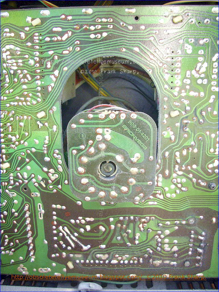
Stability is improved by use of the full balance DC feedback type differential IF amplifier
High sensitivity (Input limiting sensitivity is 32dBμ)
Large detection output (450mVrms typ, 100% mod.)
Utilizing the external resistance it can be changed freely
High S/N (77dBμ)
Wide operation supply voltage
Absolute Maximum Ratings: (T A = +25°C unless otherwise specified)
Supply Voltage, VCC . . . . . . . . . . . . . . . . . . . . . . . . . . . . . . . . . . . . . . . . . . . . . . . . . . . . . . . . . . . . . . . . . 8V
Supply Current, ICC . . . . . . . . . . . . . . . . . . . . . . . . . . . . . . . . . . . . . . . . . . . . . . . . . . . . . . . . . . . . . 36.4mA
Power Dissipation, PT . . . . . . . . . . . . . . . . . . . . . . . . . . . . . . . . . . . . . . . . . . . . . . . . . . . . . . . . . . . 450mW
Operating Ambient Temperature Range, T opr . . . . . . . . . . . . . . . . . . . . . . . . . . . . . . . . . . −20° to +75°C
Storage Temperature Range, T stg . . . . . . . . . . . . . . . . . . . . . . . . . . . . . . . . . . . . . . . . . . −55° to +125°C
The use of switching elements in electronic power supplies is
well known in the present state of the art. The advantages of such power
supplies include higher efficiency, lower weight and smaller size in
comparison to analog power supplies. At some power levels,
switching-mode power supplies are even less costly than their analog
counterparts.
The size and weight advantages of switching-mode power
supplies are achieved by operating their transformers and other magnetic
components at high frequencies. In a conventional power supply, the
transformer is operated directly from the main power source and,
accordingly, is operated at the frequency of the power source.
The
size advantages of commercial switching-mode power supplies result from
the operation of the power transformers at a frequency well above that
of standard power line frequencies. In fact, it is usually well into the
high audio frequency or ultrasonic frequency range. Dramatic
miniaturization is thus achieved, albeit at the expense of somewhat
greater circuit complexity.
For the same power levels, a
conventional transformer will vary in size approximately inversely with
frequency. As frequencies become higher and higher, cores having
suitable core loss characteristics cause the relationship to become less
favorable since the so-called "low-loss" materials may have low maximum
flux density capabilities. Thus, the core size itself will be larger
than would be predicted if a change in core material was not required.
Nonetheless, transformers having extraordinarily high volt-amp ratings
per unit volume, are made possible by operation at the high frequencies
possible with switching-mode circuitry.
Because the switching-mode
power supply is lightweight and has such superior compactness, it has
become more and more the design of choice for small, semi-portable
equipment. In fact, the use of switching-mode supplies is now being seen
in applications which were once thought to be the exclusive domain of
analog supplies such as in small digital computers, in particular those
intended for small business applications, where compactness is
considered an important attribute for ease of installation in an office
environment.
The conventional approach to design of switching-mode power supplies has been to employ a magnetically-coupled multivibrator which uses a pair of high-efficiency, solid-state switches, each alternately switching one-half of a center-tapped transformer primary to cause a square-wave having peak voltage equal to twice the center-tap voltage to appear across the entire primary. On alternate half-cycles, the primary current flows first in one side of the primary through the switch which is on, then through the other side of the primary and its associated switch, each for one-half of the period of the supplier basis operating frequency.
The search
for cost-effective ways to achieve a regulated switching-mode power
supply has led to the adoption in recent years of the blocking
oscillator and its variants as the basic power converter design.
Although somewhat touchy in terms of start-up and wide load-range
operation, the blocking oscillator is a highly efficient circuit both in
terms of its power processing efficiency and its parts cost. Instead of
a pair of switching transistors and a series-pass transistor as
required for a regulated conventional DC-DC converter, the blocking
oscillator-based power supply requires but a single switching transistor
which can be made to perform the functions of both chopping the
unregulated direct current supplied to the input, and regulating the
voltage produced at the output.
In addition to the reduction
in parts count, the blocking oscillator-based power supply can be
rendered in a design which does not require the switching transistors to
see twice the input voltage, as does the standard DC-DC converter.
Instead the power switch sees a theoretical maximum voltage of
significantly less than twice the input voltage, depending upon the duty
cycle which is chosen for its operation. Thus, operation of the supply
directly from a 220 volt rectified main power source is possible, even
using currently available semi-conductor devices
Known chopper converters of this type contain, generally connected in series between the output terminals of a D.C. power supply source (filtered rectifier), an electronic switch such as a switching transistor operating in the saturated and cut off mode and an inductor which includes the primary winding of a transformer in which at least one secondary winding supplies the A.C. energy obtained by the chopping, which is then rectified to provide the D.C. supply voltages with a ground insulated from the mains. In most of the known chopper power supplies, one can vary the output voltages by action on the cyclic ratio, i.e. the length of the saturated (closed) state of the switch, for example, by controlling periodically the transistor-chopper by means of a monostable flip-flop of variable length as a function of a voltage which may be picked up at the output of a rectifier fed by a secondary winding of the transformer so as to form a regulation loop.
Chopper power supplies have frequently been used in television receivers to eliminate the bulky and heavy mains supply transformer and make possible a regulation of the D.C. power supply voltage for this receiver. They have often been combined in particular at the output stage of the horizontal sweep circuit which supplies them with a pulse signal at the line frequency that can be used to control the chopping. Various combinations of sweep circuits and chopper power supplies have described, for example, in the French patents or patent applications with publication Nos. 2.040.217, 2.060.495, 2.167.549, 2.232.147 or 2.269.257, in which the regulation is also done by means of the variation in the cyclic ratio of the saturated and cut off states of the chopper transistor which, in some cases, is also used as the active element of the (final) output stage of the line sweep circuit or of the feeder stage which controls this circuit.
In a switch mode power supply, a first switching transistor is coupled to a primary winding of an isolation transformer. A second switching transistor periodically applies a low impedance across a second winding of the transformer that is coupled to an oscillator for synchronizing the oscillator to the horizontal frequency. A third winding of the transformer is coupled via a switching diode to a capacitor of a control circuit for developing a DC control voltage in the capacitor that varies in accordance with a supply voltage B+. The control voltage is applied via the transformer to a pulse width modulator that is responsive to the oscillator output signal for producing a pulse-width modulated control signal. The control signal is applied to a mains coupled chopper transistor for generating and regulating the supply voltage B+ in accordance with the pulse width modulation of the control signal.
Description:
The invention relates to switch-mode power supplies.
Some television receivers have signal terminals for receiving, for example, external video input signals such as R, G and B input signals, that are to be developed relative to the common conductor of the receiver. Such signal terminals and the receiver common conductor may be coupled to corresponding signal terminals and common conductors of external devices, such as, for example, a VCR or a teletext decoder.
To simplify the coupling of signals between the
external devices and the television receiver, the common conductors of
the receiver and of the external devices are connected together so that
all are at the same potential. The signal lines of each external device
are coupled to the corresponding signal terminals of the receiver. In
such an arrangement, the common conductor of each device, such as of the
television receiver, may be held "floating", or conductively isolated,
relative to the corresponding AC mains supply source that energizes the
device. When the common conductor is held floating, a user touching a
terminal that is at the potential of the common conductor will not
suffer an electrical shock.
Therefore, it may be desirable to isolate the common conductor, or ground, of, for example, the television receiver from the potentials of the terminals of the AC mains supply source that provide power to the television receiver. Such isolation is typically achieved by a transformer. The isolated common conductor is sometimes referred to as a "cold" ground conductor.
In a typical switch mode power supply (SMPS) of a television receiver the AC mains supply voltage is coupled, for example, directly, and without using transformer coupling, to a bridge rectifier. An unregulated direct current (DC) input supply voltage is produced that is, for example, referenced to a common conductor, referred to as "hot" ground, and that is conductively isolated from the cold ground conductor. A pulse width modulator controls the duty cycle of a chopper transistor switch that applies the unregulated supply voltage across a primary winding of an isolating flyback transformer. A flyback voltage at a frequency that is determined by the modulator is developed at a secondary winding of the transformer and is rectified to produce a DC output supply voltage such as a voltage B+ that energizes a horizontal deflection circuit of the television receiver. The primary winding of the flyback transformer is, for example, conductively coupled to the hot ground conductor. The secondary winding of the flyback transformer and voltage B+ may be conductively isolated from the hot ground conductor by the hot-cold barrier formed by the transformer.
It may be desirable to synchronize the operation of the chopper transistor to horizontal scanning frequency for preventing the occurrence of an objectionable visual pattern in an image displayed in a display of the television receiver.
It may be further desirable to couple a horizontal synchronizing signal that is referenced to the cold ground to the pulse-width modulator that is referenced to the hot ground such that isolation is maintained.
A synchronized switch mode power supply, embodying an
aspect of the invention, includes a transfromer having first and second
windings. A first switching arrangement is coupled to the first winding
for generating a first switching current in the first winding to
periodically energize the second winding. A source of a synchronizing
input signal at a frequency that is related to a deflection frequency is
provided. A second switching arrangement responsive to the input signal
and coupled to the second winding periodically applies a low impedance
across the energized second winding that by transformer action produces a
substantial increase in the first switching current. A periodic first
control signal is generated. The increase in the first switching current
is sensed to synchronize the first control signal to the input signal.
An output supply voltage is generated from an input supply voltage in
accordance with the first control signal.
 GENERAL BASIC TRANSISTOR LINE OUTPUT STAGE OPERATION:
The
basic essentials of a transistor line output stage are shown in Fig.
1(a). They comprise: a line output transformer which provides the d.c.
feed to the line output transistor and serves mainly to generate the
high -voltage pulse from which the e.h.t. is derived, and also in
practice other supplies for various sections of the receiver; the line
output transistor and its parallel efficiency diode which form a
bidirectional switch; a tuning capacitor which resonates with the line
output transformer primary winding and the scan coils to determine the
flyback time; and the scan coils, with a series capacitor which provides
a d.c. block and also serves to provide slight integration of the
deflection current to compensate for the scan distortion that would
otherwise be present due to the use of flat screen, wide deflection
angle c.r.t.s. This basic circuit is widely used in small -screen
portable receivers with little elaboration - some use a pnp output
transistor however, with its collector connected to chassis.
Circuit Variations:
Variations
to the basic circuit commonly found include: transposition of the scan
coils and the correction capacitor; connection of the line output
transformer primary winding and its e.h.t. overwinding
in series; connection of the deflection components to a tap on the
transformer to obtain correct matching of the components and conditions
in the stage; use of a boost diode which operates in identical manner to
the arrangement used in valve line output stages, thereby increasing
the effective supply to the stage; omission of the efficiency diode
where the stage is operated from an h.t. line, the collector -base
junction of the line output transistor then providing the efficiency
diode action without, in doing so, producing scan distortion; addition
of inductors to provide linearity and width adjustment; use of a pair of
series -connected line output transistors in some large -screen colour
chassis; and in colour sets the addition of line convergence circuitry
which is normally connected in series between the line scan coils and
chassis. These variations on the basic circuit do not alter the basic
mode of operation however.
Resonance
The
most important fact to appreciate about the circuit is that when the
transistor and diode are cut off during the flyback period - when the
beam is being rapidly returned from the right-hand side of the screen to
the left-hand side the tuning capacitor together with the scan coils
and the primary winding of the line output transformer form a parallel
resonant circuit: the equivalent circuit is shown in Fig. 1(b). The line
output transformer primary winding and the tuning capacitor as drawn in
Fig. 1(a) may look like a series tuned circuit, but from the signal
point of view the end of the transformer primary winding connected to
the power supply is earthy, giving the equivalent arrangement shown in
Fig. 1(b).
The Flyback Period:
Since the operation of the
circuit depends mainly upon what happens during the line flyback period,
the simplest point at which to break into the scanning cycle is at the
end of the forward scan, i.e. with the beam deflected to the right-hand side of the screen, see Fig. 2. At
this point the line output transistor is suddenly switched off by the
squarewave drive applied to its base. Prior to this action a linearly
increasing current has been flowing in the line output transformer
primary winding and the scan coils, and as a result magnetic fields have
been built up around these components. When the transistor is switched
off these fields collapse, maintaining a flow of current which rapidly
decays to zero and returns the beam to the centre of the screen. This
flow of current charges the tuning capacitor, and the voltage at A rises
to a high positive value - of the order of 1- 2k V in large -screen
sets, 200V in the case of mains/battery portable sets. The e
beam deflected to the right-hand side of the screen, see Fig. 2. At
this point the line output transistor is suddenly switched off by the
squarewave drive applied to its base. Prior to this action a linearly
increasing current has been flowing in the line output transformer
primary winding and the scan coils, and as a result magnetic fields have
been built up around these components. When the transistor is switched
off these fields collapse, maintaining a flow of current which rapidly
decays to zero and returns the beam to the centre of the screen. This
flow of current charges the tuning capacitor, and the voltage at A rises
to a high positive value - of the order of 1- 2k V in large -screen
sets, 200V in the case of mains/battery portable sets. The e nergy
in the circuit is now stored in the tuning capacitor which next
discharges, reversing the flow of current in the circuit with the result
that the beam is rapidly deflected to the left-hand side of the screen -
see Fig. 3. When the tuning capacitor has discharged, the voltage at A
has fallen to zero and the circuit energy is once more stored in the
form of magnetic fields around the inductive components. One half -cycle
of oscillation has occurred, and the flyback is complete.
nergy
in the circuit is now stored in the tuning capacitor which next
discharges, reversing the flow of current in the circuit with the result
that the beam is rapidly deflected to the left-hand side of the screen -
see Fig. 3. When the tuning capacitor has discharged, the voltage at A
has fallen to zero and the circuit energy is once more stored in the
form of magnetic fields around the inductive components. One half -cycle
of oscillation has occurred, and the flyback is complete.
Energy Recovery:
First
Part of Forward Scan The circuit then tries to continue the cycle of
oscillation, i.e. the magnetic fields again collapse, maintaining a
current flow which this time would charge the tuning capacitor
negatively (upper plate). When the voltage at A reaches about -0.6V
however the efficiency diode becomes forward biased and switches on.
This damps the circuit, preventing further oscillation, but the magnetic
fields continue to collapse and in doing so produce a linearly decaying
current flow which provides the first part of the forward s can,
the beam returning towards the centre of the screen - see Fig. 4. The
diode shorts out the tuning capacitor but the scan correction capacitor
charges during this period, its right-hand plate becoming positive with
respect to its left-hand plate, i.e. point A. Completion of Forward Scan
When the current falls to zero, the diode will switch off. Shortly
before this state of affairs is reached however the transistor is
switched on. In practice this is usually about a third of the way
through the scan. The squarewave applied to its base drives it rapidly
to saturation, clamping the vol
can,
the beam returning towards the centre of the screen - see Fig. 4. The
diode shorts out the tuning capacitor but the scan correction capacitor
charges during this period, its right-hand plate becoming positive with
respect to its left-hand plate, i.e. point A. Completion of Forward Scan
When the current falls to zero, the diode will switch off. Shortly
before this state of affairs is reached however the transistor is
switched on. In practice this is usually about a third of the way
through the scan. The squarewave applied to its base drives it rapidly
to saturation, clamping the vol tage
at point A at a small positive value - the collector emitter saturation
voltage of the transistor. Current now flows via the transistor and the
primary winding of the line output transformer, the scan correction
capacitor discharges, and the resultant flow of current in the line scan
coils drives the beam to the right-hand side of the screen see Fig. 5.
tage
at point A at a small positive value - the collector emitter saturation
voltage of the transistor. Current now flows via the transistor and the
primary winding of the line output transformer, the scan correction
capacitor discharges, and the resultant flow of current in the line scan
coils drives the beam to the right-hand side of the screen see Fig. 5.
Efficiency:
The
transistor is then cut off again, to give the flyback, and the cycle of
events recurs. The efficiency of the circuit is high since there is
negligible resistance present. Energy is fed into the circuit in the
form of the magnetic fields that build up when the output transistor is
switched on. This action connects the line output transformer primary
winding across the supply, and as a result a linearly increasing current
flows through it. Since the width is
dependent on the supply voltage, this must be stabilised.
Harmonic Tuning:
There
is another oscillatory action in the circuit during the flyback period.
The considerable leakage inductance between the primary and the e.h.t.
windings of the line output transformer, and the appreciable self
-capacitance present, form a tuned circuit which is shocked into
oscillation by the flyback pulse. Unless this oscillation is controlled,
it will continue into and modulate the scan. The technique used to
overcome this effect is to tune the leakage inductance and the
associated capacitance to an odd harmonic of the line flyback
oscillation frequency. By doing this the oscillatory actions present at
the beginning of the scan cancel. Either third or fifth harmonic tuning
is used. Third harmonic tuning also has the effect of increasing the
amplitude of the e.h.t. pulse, and is generally used where a half -wave
e.h.t. rectifier is employed. Fifth harmonic tuning results in a
flat-topped e.h.t. pulse, giving improved e.h.t. regulation, and is
generally used where an e.h.t. tripler is employed to produce the e.h.t.
The tuning is mainly built into the line output transformer, though an
external variable inductance is commonly found in colour chassis so that
the tuning can be adjusted. With a following post I will go into the
subject of modern TV line timebases in greater detail with other models
and technology shown here at Obsolete Technology Tellye !
integrated circuit FM AM Radio Receiver System Double-converting FM tuner
Hitachi, Ltd. (JP)
ear at
the output of the second mixer conduit. When the higher harmonic
components at the output of the second mixer circuit are injected into
an FM demodulator circuit, beat trouble is induced. The second frequency
converter circuit is also constructed in the form of an integrated
circuit, and filter means to pass the fundamental waves of a first
intermediate frequency signal and to reject the higher harmonic
frequency components thereof is connected between the output of the
first intermediate frequency amlifier stage executing the amplitude
limiting operation and the input of the second mixer circuit, whereby
the beat trouble can be prevented. "Denpa Kagaku", (Electric Wave Science), Jan. 1977, vol. 532, pp. 161-165.
an antenna;
a radio frequency amplifier circuit for amplifying an FM radio frequency signal received at said antenna;
a first frequency converter circuit which is made up of a first mixer circuit and a first local oscillator circuit and which generates a first intermediate frequency signal from said FM radio frequency signal and a first local oscillation frequency signal generated at said first local oscillator circuit;
a first filter means for deriving said first intermediate frequency signal from said first frequency converter circuit;
a first intermediate frequency amplifier circuit coupled to said first filter means for amplifying said first intermediate frequency signal and limiting the amplitude of said first intermediate frequency signal to a constant magnitude, said first intermediate frequency amplifier circuit being constructed in the form of a first semiconductor integrated circuit having first and second operating-voltage-feeding external terminals for supplying an operating voltage therebetween;
a second filter means coupled to said first intermediate frequency amplifier circuit for passing said first intermediate frequency signal therethrough and rejecting higher harmonic frequency components of said first intermediate frequency signal amplitude-limited by said first intermediate frequency amplifier circuit;
a second frequency converter circuit which is made up of a second mixer circuit and a second local oscillator circuit and which generates a second intermediate frequency signal from said first intermediate frequency signal derived through said second filter means and a second local oscillation frequency signal generated at said second local oscillator circuit, said second frequency converter circuit being constructed in the form of a second semiconductor integrated circuit having first and second operating-voltage-feeding external terminals for supplying an operating voltage therebetween;
a pulse count type FM demodulator circuit for obtaining an FM demodulation output signal from said second intermediate frequency signal, said pulse count type FM demodulator circuit being constructed in the form of a third semiconductor integrated circuit having first and second operating-voltage-feeding external terminals for supplying an operating voltage therebetween; and
decoupling filter means for connecting respective ones of said first operating-voltage-feeding external terminals of the first and second semiconductor integrated circuits to said first operating-voltage-feeding external terminal of the third semiconductor integrated circuit and for preventing an undesired signal generated at said first operating-voltage-feeding external terminal of the third semiconductor integrated circuit from being transferred to said respective ones.
2. A double-converting FM tuner according to claim 1, wherein said decoupling filter means comprises a first filter means connected between said first operating-voltage-feeding external terminals of the first and third semiconductor integrated circuit, and a second filter means between said first operating-voltage-feeding external terminals of the second and third semiconductor integrated circuits.
3. A double-converting FM tuner according to claim 1, wherein said decoupling filter means is made of an inductor and a capacitor.
4. In a double-converting type FM tuner comprising:
a radio frequency amplifier circuit for amplifying an FM radio frequency signal;
a first frequency converter circuit for receiving the output signal of said radio frequency amplifier stage and generating a first FM intermediate frequency signal having a first intermediate frequency from said FM radio frequency signal and a first local oscillation signal generated therein;
a first filter means, coupled to said first frequency converter circuit and tuned to said first intermediate frequency, for deriving said first FM intermediate frequency signal from said first frequency converter circuit;
a first amplitude-limiting amplifier circuit consisting of a plurality of cascaded amplifier stages for amplifying said first FM intermediate frequency signal derived from said first filter means and limiting the amplitude of said first FM intermediate frequency signal to a constant magnitude at the final amplifier stage thereof, said first amplitude-limiting amplifier circuit being constructed in the form of a semiconductor integrated circuit;
a second filter means, coupled to the final amplifier stage of said first amplitude-limiting amplifier circuit, for receiving the amplitude-limited first FM intermediate frequency signal and rejecting higher harmonic frequency components of the amplitude-limited first FM intermediate frequency signal;
a second frequency converter circuit for receiving said first FM intermediate frequency signal derived from said second filter means and generating a second FM intermediate frequency signal having a second intermediate frequency from said first FM intermediate frequency signal and a second local oscillation signal generated therein, said second frequency converter circuit being constructed in the form of a semiconductor integrated circuit;
a third filter means, coupled to said second frequency converter circuit, for deriving said second FM intermediate frequency signal from said second frequency converter circuit; and
an FM demodulator circuit, coupled to said third filter means, for obtaining an FM demodulation output signal from said second FM intermediate frequency signal, said FM demodulator circuit is constructed in the form of a semiconductor integrated circuit,
the improvement wherein each of said semiconductor integrated circuits for said first amplitude-limiting amplifier circuit, second frequency converter circuit and FM demodulator circuit independently has a power supply external terminal for connecting an operating voltage source thereto, and wherein respective ones of said power supply external terminals for said first amplitude-limiting amplifier circuit and second frequency converter circuit are connected to said power supply external terminal for said FM demodulator circuit through decoupling filter means for decoupling said respective ones to said power supply external terminal for said FM demodulator circuit.
5. A double-converting FM tuner according to claim 4, wherein said decoupling filter means is made of an inductor and a capacitor.
6. A double-converting FM tuner according to claim 5, wherein said FM demodulator circuit is a pulse count type FM demodulator circuit.
7. A double-converting FM tuner according to claim 4, wherein each of said first amplitude-limiting amplifier circuit, second frequency converter circuit and FM demodulator circuit is supplied with an operating voltage through a voltage regulator from said power supply external terminal thereof.
8. A double-converting FM tuner according to claim 4, wherein said first amplitude-limiting amplifier circuit is constructed in the form of a first semiconductor integrated circuit having a first semiconductor substrate, while said second frequency converter circuit and said FM demodulator circuit are constructed in the form of a second semiconductor integrated circuit having a second semiconductor substrate different from said first semiconductor substrate.
BACKGROUND OF THE INVENTION
This invention relates to a double-converting FM tuner.
Heretofore, a double-converting FM tuner has been constructed of an antenna, a radio frequency amplifier stage, a first frequency converter circuit composed of a first mixer circuit and a first local oscillator circuit, a first intermediate frequency filter, a first intermediate frequency amplifier stage, a second frequency converter circuit composed of a second mixer circuit and a second local oscillator circuit, a second intermediate frequency filter, and a demodulator circuit.
As in
the case of the superheterodyne system, the double-converting system is
prone to cause beat troubles. This is particularly true where an output
signal of the first intermediate frequency amplifier stage is
limit-amplified which results in the square pulse output current thereof
containing large quantities of higher harmonic components. This leads
to the disadvantage that the l-th order higher harmonics of the output
current of the first intermediate frequency amplifier stage and the m-th
order higher harmonics in the output current of the second local
oscillator circuit or the n-th order higher harmonics of the second
intermediate frequency give rise to cross modulation in the demodulator
circuit. These difficulties appear at the output of the demodulator
circuit. (Letters l, m and n denote positive integers.)
Usually, the second intermediate frequency filter operates normally at frequencies up to several tens of MHz. For frequencies from several tens of MHz to several hundred MHz, however, a sufficient decay is not attained in the rejection region of the filter on account of the characteristics of circuit components, etc. Accordingly, to inject the output current of the first intermediate frequency amplifier stage containing the large quantities of higher harmonic components directly into the second mixer circuit results in more higher harmonic components than are generated in the second frequency converter circuit when a first intermediate frequency signal not containing such higher harmonic components is supplied. The higher harmonic components increase the quantity of spurious waves to be mixed into the demodulator circuit so that the beat trouble is prone to occur. It has been revealed by the inventor that this phenomenon becomes especially conspicuous when the frequency converter circuits and the demodulator circuit are assembled within an identical semiconductor integrated circuit.
SUMMARY OF THE INVENTION
This invention has for its object to provide a double-converting FM tuner utilizing the semiconductor integrated circuit technology in which higher harmonic components existant in the square pulse waveform output of a first intermediate frequency amplifier stage e

xecuting a limit-amplifying operation are prevented from being mixed into a demodulator. The resultant tuner is free from beat troubles.
BRIEF DESCRIPTION OF THE DRAWING
FIG. 1 shows circuit blocks of a double-converting FM tuner embodying this invention.
DESCRIPTION OF THE PREFERRED EMBODIMENT
Hereunder, a preferred embodiment of this invention will be described.
Referring to FIG. 1, numeral 1 designates an antenna, numeral 2 an RF (radio frequency) amplifier stage, numeral 3 a first mixer circuit, numeral 4 a first local oscillator circuit, numeral 5 a first IF (intermediate frequency) filter, numeral 6 a first IF amplifier stage, numeral 7 a second mixer circuit, numeral 8 a second local oscillator circuit, numeral 9 a second IF filter, numeral 10 a detector circuit, and numeral 11 an additional first IF filter which resonates with a first intermediate frequency. A first frequency converter circuit is constructed of the first mixer circuit 3 and the first local oscillator circuit 4, while a second frequency converter circuit is constructed of the second mixer circuit 7 and the second local oscillator circuit 8. Shown at 12 is a limiting amplifier circuit which limit-amplifies a signal voltage applied to the detector circuit 10.
The RF amplifier stage 2 subjects to voltage amplification an FM radio frequency signal which has been received by the antenna 1. The first mixer circuit 3 effects the frequency mixing between an amplified FM radio frequency output signal at the output of the RF amplifier stage 2 and a first local oscillation output signal at the output of the first local oscillator circuit 4, thereby to transmit a first intermediate frequency signal of 10.7 MHz to the first IF filter 5. Preferably, the first IF filter 5 is constructed of an intermediate frequency transformer and a ceramic filter, and it has a predetermined frequency band width.
The first IF amplifier stage 6 to which the first IF signal of 10.7 MHz is applied includes three stages of cascaded differential amplifier circuits 60, 61 and 62 and a voltage regulator 63. It is formed within a single silicon semiconductor substrate by the well-known techniques for manufacturing semiconductor integrated circuits. The first semiconductor integrated circuit which includes the first IF amplifier stage 6 is indicated by broken lines l1. The two differential inputs 600 and 601 of the first-stage differential amplifier circuit 60 are respectively connected to input terminals P18 and P19 of the first semiconductor integrated circuit, and are connected with each other through a resistor R1. The 601 input of the two differential inputs is A.C. grounded A.C.-wise by a capacitor C1. The two differential outputs 602 and 603 of the first-stage differential amplifier circuit 60 are respectively applied to the two differential inputs 610 and 611 of the second-stage differential amplifier circuit 61 through internal interconnections inside the first semiconductor integrated circuit. Likewise, the two differential outputs 612 and 613 of the second-stage differential amplifier circuit 61 are respectively applied to the two differential inputs 620 and 621 of the third-stage differential amplifier circuit 62 through internal interconnections inside the first semiconductor integrated circuit. Further, the two differential outputs 622 and 623 of the third-stage differential amplifier circuit 62 are respectively applied to output terminals P20 and P21 of the first semiconductor integrated circuit through internal interconnections inside this integrated circuit.
According to the principle of this invention, the additional first IF filter 11 is especially connected between the output terminal P20 of the first IF amplifier stage 6 and an input terminal P15 of the second frequency converter circuit.
As
this first IF filter 11, there can be used a filter which passes the
first intermediate frequency of 10.7 MHz therethrough and which rejects
the higher harmonic frequency components of the first intermediate
frequency, for example, a resonance circuit whose resonance frequency is
the first intermediate frequency.
In order to avoid the undesirable RF signal crosstalk between the second frequency converter circuit or the detector circuit 10 and the first IF amplifier stage 6, according to the preferred embodiment of this invention, the detector circuit 10 and the second frequency converter circuit made up of the second mixer circuit 7 and the second local oscillator circuit 8 are formed within a second semiconductor integrated circuit which employs another silicon semiconductor substrate different from the silicon semiconductor substrate of the first semiconductor integrated circuit. The second semiconductor integrated circuit is indicated by broken lines l2.
The second mixer circuit 7 executes the frequency mixing between an amplified first IF signal of 10.7 MHz provided at the input terminal P15 of the second semiconductor integrated circuit through the first IF filter 11 and a second local oscillation output signal of 8.735 MHz at an output 80 of the second local oscillator circuit 8, thereby to transmit a second intermediate frequency signal of 1.965 MHz to a terminal P1 of the second semiconductor integrated circuit. The oscillation frequency of the second local oscillator circuit 8 is determined by capacitors C5 and C6 and inductors L5 and L6 of a frequency selector circuit 15 which is connected between terminals P16 and P17. The second IF filter 9 which has a passing band width of 1 MHz-4 MHz is connected between the terminal P1 and another terminal P4.
A second IF signal provided at the terminal P4 has a substantially sinusoidal waveform. It is amplified by the limiting amplifier 12 formed within the second semiconductor integrated circuit and having a high voltage gain, with the result that it is converted into a square pulse waveform. The second IF signal in the square pulse waveform at the output of the limiting amplifier 12 is applied to the pulse count type FM detector 10 which is also formed within the second semiconductor integrated circuit. The pulse count type FM detector 10 is constructed of a trigger circuit 100, a monostable multivibrator 110, an inverter 120, a capacitor C2 which is connected between an output terminal P9 of the monostable multivibrator 110 and an input terminal P10 of the inverter 120 outside the second integrated circuit, and a resistor R2 which is connected between the terminal P10 and a terminal P11.
The trigger circuit 100 transmits to the monostable multivibrator 110 a trigger pulse of narrow pulse width on the basis of the second IF signal in the square pulse waveform. The monostable multivibrator 110 is driven by the trigger pulse, and transmits to the inverter 120 a pulse signal having a fixed pulse width which is a decided by the time constant between the capacitor C2 and the resistor R2. A square pulse signal of the fixed pulse width having pulse intervals corresponding to the FM modulation is provided at an output terminal P8 of the inverter 120. By connecting appropriate smoothing means to the terminal P8, and FM demodulation output signal is obtained.
On the one hand, the overall voltage gain of the three stages of differential amplifier circuits 60, 61 and 62 constituting the first IF amplifier stage 6 is sufficiently high, so that the first IF signal applied to the terminal P18, having the sinusoidal waveform of 10.7 MHz, is sufficiently amplified by the first IF amplifier stage 6. The amplified first IF signal to be provided at the output terminals P20 and P21 is accordingly clipped in a square pulse waveform. Thus, the first IF amplifier stage 6 operates as an amplitude-limiting amplifier. Any undesired AM signal component contained in the received FM signal can be removed owing to the amplitude-limiting operation of the first IF amplifier stage 6.
However, the amplified first IF signal of 10.7 MHz in the square pulse waveform as obtained at the terminal P20 has the fundamental wave component of 10.7 MHz and higher harmonic components of higher frequencies.
Thus, on the other hand, the first IF filter 11 which passes the first intermediate frequency of 10.7 MHz therethrough and which stops the passage of the higher harmonic frequencies is connected between the output terminal P20 of the first IF amplifier stage 6 and the input terminal P15 of the second frequency converter circuit. Therefore, the higher harmonic components in the output of the first IF amplifier stage, 6 which creates the beat trouble, are removed by the first IF filter 11, and the higher harmonic components to be injected into the detector circuit 10 can be sufficiently reduced so that cross modulation is prevented.
Further, in case where the FM demodulator circuit 10 is of the pulse count type, a large detection current responsive to the second IF signal flows through this demodulator circuit. In general, an internal interconnection inside a semiconductor integrated circuit is formed of an evaporated metallic thin film and therefore has an equivalent resistance value which is not negligible. In contrast, an external interconnection to be connected outside the semiconductor integrated circuit exhibits only an equivalent resistance of a negligibly small value because a metal wire of high conductivity can be utilized.
The large detection current flows through a supply
voltage-feeding internal interconnection and a grounding internal
interconnection for the FM demodulator circuit 10. In consequence,
voltage drops which respond to the second IF signal of 1.965 MHz and
which are not negligible appear in these internal interconnections
inside the semiconductor integrated circuit.
If the supply voltage-feeding internal interconnection or grounding internal interconnection of the FM demodulator circuit 10 is connected in common with a supply voltage-feeding internal interconnection or grounding internal interconnection for the second frequency converter circuit by means of an internal interconnection inside the semiconductor integrated circuit, the voltage drop which is not negligible as stated above will be transmitted to the supply voltage-feeding internal interconnection or grounding internal interconnection of the second frequency converter circuit.
Further, if the supply voltage-feeding internal interconnection or grounding internal interconnection of the FM demodulator circuit 10 is connected in common with a supply voltage-feeding internal interconnection or grounding internal interconnection for the first IF amplifier stage 6 by means of an internal interconnection inside the semiconductor integrated circuit, the voltage drop which is not negligible as stated above will be transmitted to the internal interconnection quite similarly.
The transmissions of the voltage drops which respond to the second intermediate frequency of 1.965 MHz and which are not negligible will give rise to the cross modulation between the transmitted signal of 1.965 MHz and the first IF signal of 10.7 MHz inside the first IF amplifier stage 6, and will give rise to the composite cross modulation among the transmitted signal of 1.965 MHz, the first IF signal of 10.7 MHz and the second local oscillation signal of 8.735 MHz inside the second frequency converter circuit. These cross modulations will generate higher harmonic signal components of high frequencies which similarly form the cause of beat trouble, at the output terminal P20 of the first IF amplifier stage 6 and the output terminal P1 of the second mixer circuit 7.
According to the preferred embodiment of this invention, in order to avoid the cross modulations, the transmissions of the undesired voltage drops above described are prevented. More specifically, a supply voltage-feeding internal interconnection 102 and a grounding internal interconnection 103 for the FM demodulator circuit 10 and the limiting amplifier circuit 12 are respectively connected to a supply voltage-feed terminal P12 and a ground terminal P14 of the second semiconductor integrated circuit. The supply voltage-feed terminal P12 and the ground terminal P14 are respectively connected to a common power supply terminal 15 and the ground point GND through external interconnections. A voltage regulator 14 is arranged between the supply voltage-feed terminal P12 and the supply voltage-feeding internal interconnection 102, and delivers to a terminal 141 an operating voltage which is substantially constant against fluctuations in a voltage Vcc supplied to the common power supply terminal 16. A ground terminal 143 of the voltage regulator 14 is also connected to the ground terminal P14 of the second semiconductor integrated circuit through an internal interconnection.
A supply voltage-feeding internal interconnection 782 and a grounding internal interconnection 783 of the second frequency converter circuit, namely, the second mixer circuit 7 and the second local oscillator circuit 8 are respectively connected to another supply voltage feed terminal P3 and another ground terminal P2 of the second semiconductor integrated circuit. The ground terminal P2 is connected to the ground point GND through an external interconnection. A voltage regulator 13 is arranged between the supply voltage-feeding terminal P3 and the supply voltage-feeding internal interconnection 782, and delivers a substantially constant operating voltage to a terminal 131. A ground terminal 133 of this voltage regulator 13 is also connected to the ground terminal P2 of the second semiconductor integrated circuit through an internal interconnection.
The first IF amplifier stage 6 is formed within the first semiconductor integrated circuit as stated above, and a supply voltage-feeding internal interconnection 64 and a grounding internal interconnection 65 thereof are respectively connected to a supply voltage-feed terminal P22 and a ground terminal P23 of the first semiconductor integrated circuit. The ground terminal P23 is connected to the ground point GND through an external interconnection. A voltage regulator 63 is arranged between the supply voltage feed terminal P22 and the supply voltage-feeding internal interconnection 64, and delivers a substantially constant operating voltage to a terminal 631 similarly to the above. A ground terminal 633 of the voltage regulator 63 is also connected to the ground terminal P23 of the first semiconductor integrated circuit through an internal interconnection.
More preferably, a filter composed of an inductor L3 and a capacitor C3 and a filter composed of an inductor L4 and a capacitor C4 are respectively connected between the supply voltage-feed terminal P12 and the supply voltage-feed terminal P3 and between the former terminal P12 and the supply voltage-feed terminal P22. Thus, the transmissions of the voltages responsive to the detection current previously stated can be further reduced.
PHILIPS 10CX1100 PHILITINA COLOR 1100 CHASSIS (SHARP) Electronic tuning type television receiver:
Hitachi, Ltd. (JP)
tuning detection circuit for generating a signal when said tuning circuit is tuned to the selected channel, wherein tuning voltage control means are provided for alternately increasing and decreasing, at a predetermined rate, the digital data read out from said memory means to sequentially apply a signal representative of said alternately increased and decreased data to said D/A converter, and for ceasing the increasing and decreasing operation in response to the appearance of an output from said tuning detection circuit.2. An electronic tuning type television receiver comprising a tuning circuit including a local oscillator whose oscillation frequency is controlled to be variable depending on a voltage applied to a variable capacitance diode, signal input means for specifying a selected channel, memory means for storing digital data indicative of tuning voltages corresponding to a plurality of channels respectively so that a tuning voltage corresponding to a selected channel can be applied to said variable capacitance diode in said tuning circuit, means for reading out from said memory means the digital data corresponding to the selected channel specified by said signal input means, a D/A converter converting the digital data read out from said memory means to an analog signal which is applied to said variable capacitance diode, and a tuning detection circuit detecting the fact that said tuning circuit is tuned to the selected channel, wherein the improvement comprises tuning voltage control means which functions to sequentially modify, at a predetermined rate, the digital data read out from said memory means to sequentially apply such a signal to said D/A converter, and which ceases its data modifying operation in response to the appearance of an output from said tuning detection circuit, and
wherein said tuning voltage control means comprises means for generating a train of clock pulses, counter means starting to count said clock pulses under control of said means for reading out the digital data from said memory means, and arithmetic operation means for adding or subtracting the count of said counter means to or from the digital data read out from said memory means, the output of said arithmetic operation means being applied to said D/A converter.
3. An electronic tuning type television receiver comprising a tuning circuit including a local oscillator whose oscillation frequency is controlled to be variable depending on a voltage applied to a variable capacitance means, signal input means for specifying a selected channel, memory means for storing digital data indicative of tuning voltages corresponding to a plurality of channels respectively so that a tuning voltage corresponding to a selected channel can be applied to said variable capacitance means in said tuning circuit, means for reading out from said memory means the digital data corresponding to the selected channel specified by said signal input means, a D/A converter converting the digital data read out from said memory means to an analog signal which is applied to said variable capacitance means, a tuning detection circuit generating a signal when said tuning circuit is tuned to the selected channel, means to generate an alternately varying signal to control digital data being read out from said memory to said D/A converter, means to sequentially change the value of said digital data in accordance with said alternately varying signal, and means responsive to said signal at the output of said tuning detection circuit to cease generation of said alternately varying signal.
Description:
BACKGROUND OF THE INVENTION
This invention relates to a television receiver of electronic tuning type.
In a television receiver of electronic tuning type, a local oscillator in its tuning circuit includes a variable capacitance diode, and a tuning voltage corresponding to a specific channel selected by a TV viewer is applied to this variable capacitance diode so that the tuning circuit can be tuned to the selected channel frequency. In the television receiver of this type, a plurality of digital data indicative of tuning voltage values corresponding to a plurality of channels respectively are stored previously in a tuning data memory, and a digital data corresponding to a specific channel selected by a TV viewer is read out from the memory to be subjected to D/A conversion in a D/A converter thereby providing an analog voltage or tuning voltage which is applied to the variable capacitance diode in the local oscillator of the tuning circuit.
However, the operating characteristic of the variable capacitance diode in the television receiver of this type tends to vary with time, due to, for example, a temperature drift and a secular variation. As a result of such a variation in the operating characteristic of the variable capacitance diode, a deviation of each individual optimum tuning point takes place for the tuning circuit with the corresponding tuning voltage data stored in the tuning data memory, and a clear picture will not be reproduced on the screen of the CRT.
SUMMARY OF THE INVENTION
It is an object of the present invention to provide an improved electronic tuning type television receiver whose tuning circ
uit can be reliably and accurately tuned to a selected channel regardless of such a variation in the operating characteristic of the variable capacitance diode in the local oscillator of the tuning circuit.Another object of the present invention is to provide an improved electronic tuning type television receiver in which the digital data indicative of the individual tuning voltages stored initially in the tuning data memory need not be renewed or rewritten later, and the optimum tuning voltage can always be applied to the variable capacitance diode when the corresponding channel is selected.
In accordance with the present invention which attains the above objects, there is provided an electronic tuning television receiver comprising a tuning circuit including a local oscillator whose oscillation frequency is controlled to be variable depending on a voltage applied to a variable capacitance diode, signal input means for specifying a selected channel, memory means for storing a plurality of digital data indicative of tuning voltages corresponding to a plurality of channels respectively so that a tuning voltage corresponding to a selected channel can be applied to the variable capacitance diode in the tuning circuit, means for reading out from the memory means the digital data corresponding to the selected channel specified by the signal input means, a D/A converter converting the digital data read out from the memory means into an analog signal which is applied to the variable capacitance diode, and a tuning detection circuit detecting the fact that the tuning circuit is turned to the selected channel, wherein the improvement comprises tuning voltage control means which functions to sequentially modify, at a predetermined rate, the digital data read out from the memory means to sequentially apply such a signal to the D/A converter, and which ceases its data modifying operation in response to the appearance of an output from the tuning detection circuit.
Various further and more specific objects, features and advantages of the present invention will appear from the description given below, taken in connection with the accompanying drawings illustrating, by way of example, preferred embodiments of this invention.
BRIEF DESCRIPTION OF THE DRAWINGS
FIG. 1 is a block circuit diagram showing principal parts of a preferred embodiment of the electronic tuning type television receiver according to the present invention.
FIG. 2 is a block circuit diagram showing in detail the structure of the channel selection input control circuit and the tuning data memory designated by the blocks 8 and 9 respectively in FIG. 1.
FIG. 3 is a diagrammatic view illustrating the tuning voltage control operation of the tuning voltage control circuit designated by the block 10 in FIG. 1.
FIG. 4 is a block circuit diagram showing in detail the structure of the tuning voltage control circuit.
FIG. 5 is a time chart of various signals and data applied to and delivered from the tuning voltage control circuit.
DESCRIPTION OF THE PREFERRED EMBODIMENTS
FIG. 1 is a block circuit diagram showing principal parts of a preferred embodiment of the electronic tuning type television receiver according to the present invention. Referring to FIG. 1, an antenna 1 is connected to a tuning circuit 2. This tuning circuit 2 includes a high-frequency amplifier 3, a mixer 4 and a local oscillator 5. This local oscill
 ator 5 is of a variable frequency oscillation type in which at least one variable capacitance diode is used as its tuning element. A video intermediate frequency signal S appears at the output of the mixer 4 to be applied to a video system including a video intermediate frequency amplifier and a video detector, which are well known in the art and have not any direct concern with the present invention. Therefore, any detailed description of these elements will be unnecessary.
A tuning detection signal Sh appears from a tuning detection circuit 6 when this circuit 6 detects appearance of the video intermediate frequency signal S from the mixer 4. This tuning detection circuit 6 includes, for example, a frequency discriminating circuit connected to the video intermediate frequency amplifier, and the tuning detection signal Sh appears at the output of the tuning detection circuit 6 when the output signal of the frequency discriminating circuit lies within a predetermined voltage range, and the level of the output signal of the video intermediate frequency amplifier is higher than a predetermined setting, with the horizontal synchronizing signal being present at the same time. Such a tuning detection circuit 6 is disclosed in, for example, Japanese Utility Model Application No. 33295/78, filed on Mar. 17, 1978 in the name of Hitachi, Ltd. The electronic tuning television receiver shown in FIG. 1 further comprises a channel selection input switch 7, a channel selection input control circuit 8, a tuning data memory 9, a tuning voltage control circuit 10 which is a characteristic part of the present invention, and a D/A converter 11.
Referring to FIG. 2, the channel selection input control circuit 8 includes an encoder 20, a latch circuit 21, an OR gate 23 and a pulse generating circuit 24, and the tuning data memory 9 includes an address decoder 22 and a data storage 25.
When a channel is selected, a channel selection input signal Sa is applied from the channel selection input switch 7 to the encoder 20 in the channel selection input control circuit 8 to be converted into a corresponding binary-coded signal Sa ' which is applied through the latch circuit 21 to the address decoder 22 in the tuning data memory 9.
The data storage 25 in the tuning data memory 9 is in the form of a non-volatile memory which is featured by the fact that data once written therein can be stored permanently unless an erase signal is applied thereto. Data b1 indicative of tuning voltages corresponding to the individual channels and data b2 indicative of either the VHF band or the UHF band are stored in the data storage 25 of the tuning data memory 9. Therefore, when one of the channels is selected by a TV viewer who actuates the corresponding channel selection button of the channel selection input switch 7, access to the corresponding data area of the data storage 25 is provided by the output signal of the address decoder 22, so that a data signal Sb including the tuning voltage data b1 and band data b2 corresponding to the selected channel appears from the tuning data memory 9.

In the channel selection input control circuit 8, the signal portion indicative of the individual bits of the binary-coded output signal Sa ' of the encoder 20 are applied to the OR gate 23, and the pulse generating circuit 24 generates a pulse signal Sc including a single pulse when the output signal from the OR gate 23 is in its logic "1". Such a pulse signal Sc appears each time a channel is selected, to be applied to the tuning voltage control circuit 10 as a control starting signal.
According to the present invention, the tuning voltage control circuit 10 controls the tuning voltage so as to modify it in a manner as, for example, shown in FIG. 3. More precisely, when a tuning voltage Vo indicated by a digital data b1 read out from the tuning data memory 9 deviates from a voltage VF representing the actual tuning voltage range of the tuning circuit 2 for the television receiver as shown in FIG. 3 due to, for example, a secular variation in the operating characteristic of the variable capacitance diode, a predetermined, stepwise increasing value is alternately added to or subtracted from the reference value Vo produced from the read out digital data in the tuning voltage control circuit 10 until finally a proper tuning voltage within the range VF is applied across the variable capacitance diode, that is, until the optimum tuning point is reached.
FIG. 4 shows the practical structure of one form of the tuning voltage control circuit 10 adapted to carry out such a manner of tuning voltage control. Referring to FIG. 4, the tuning voltage control circuit 10 comprises a clock pulse generator 30 generating a train of clock pulses in response to the application of the control starting signal Sc from the channel selection input control circuit 8, a clock pulse counter 31 counting clock pulses applied thereto, an adder/subtractor circuit 32 adding or subtracting the count output signal Sl of the clock pulse counter 31 to or from the tuning voltage data b1 in the data signal Sb, AND gates 33, 36, a flip-flop circuit 34, an inverter 35, and a NOR gate 37. The output signal Sd of the adder/subtractor circuit 32 is applied to the D/A converter 11 shown in FIG. 1. The pulse signal generated from the pulse generator 30 is applied to the AND gate 33 which is controlled by an inverted signal of the tuning detection signal Sh, so that the AND gate 33 ceases to provide its output pulse signal Si after the tuning detection signal Sh has been applied thereto.

The clock pulse signal Si appearing at the output of the AND gate 33 is applied to the trigger terminal of the flip-flop circuit 34 as a data input timing signal, and the output signal Sj of this flip-flop circuit 34 is fed back to its data terminal through the inverter 35. Thus, the state of the flip-flop circuit 34 is inverted each time a pulse of the pulse signal Si is applied to its trigger terminal. The output signal Sj of the flip-flop circuit circuit 34 is applied also to the adder/subtractor circuit 32 as an operation mode specifying signal, and depending on the state or level of the output signal Sj of the flip-flop circuit 34, the adder/subtractor circuit 32 alternately adds the count output Sl of the clock pulse counter 31 to the data b1 or subtracts the count output Sl of the clock pulse counter 31 from the data b1, and the resultant digital data signal Sd obtained by the addition or subtraction in the adder/subtractor 32 is applied to the D/A converter 11 (FIG. 1).
The clock pulse signal Si appearing at the output of the AND gate 33 is applied to the AND gate 36 together with the output signal Sj of the flip-flop circuit 34. Consequently, a clock pulse signal Sk including clock pulses, each of which appears when the signal Sj is in logic "1", is applied to the clock pulse counter 31, so that the count of the clock pulse counter 31 is changed upon completion of both the addition and the subtraction in the adder/subtractor circuit 32.
Both the clock pulse counter 31 and the flip-flop circuit 34 are cleared or reset by the control starting signal Sc. The control starting signal Sc is applied, together with the output pulse signal Si of the AND gate 33, to the NOR gate 37 which generates an output signal Se which is applied to the D/A converter 11 (FIG. 1) as a data receiving timing signal. The D/A converter 11 receives the digital data signal Sd responsive to rising of the pulse signal Se and converts this digital data signal Sd into an analog signal Sg which is applied to the variable capacitance diode in the local oscillator 5. The data b2 included in the data signal Sb to specify the frequency band is applied to the tuning circuit 2 as a band specifying signal Sf.
The operation of the tuning voltage control circuit 10 having the construction illustrated in FIG. 4 will be described in further detail with reference to a signal time chart shown in FIG. 5. The data signal Sb including the data b1 and b2 appears from the tuning data memory 9 in response to the application of the channel selection input signal Sa from the channel selection input switch 7 to the channel selection input control circuit 8 and is applied to the tuning voltage control circuit 10 together with the control starting signal Sc.
In the tuning voltage control circuit 10, the clock pulse signal Si appears from the AND gate 33 in response to the application of the control starting signal Sc to the pulse generator 30, and both the flip-flop circuit 34 and the clock pulse counter 31 are reset or cleared responsive to the rising of the control starting signal Sc. Thereafter, the output signal Sj of the flip-flop circuit 34 is repeatedly inverted in its level at the rise time of successive pulses of the pulse signal Si, and such a pulse signal Sj is applied to the AND gate 36 together with the pulse signal Si, so that the clock pulse signal Sk representing the logical product of the two input signals Si and Sj appears at the output of the AND gate 36 to be applied to the clock pulse counter 31. Consequently, the count indicated by the output signal Sl of the clock pulse counter 31 changes at a cycle which is 1/2 of the cycle of the pulse signal Si. In FIG. 5, the value of the tuning voltage data b1 read out from the tuning data memory 9 is shown by the symbol A. In the adder/subtractor circuit 32, the data indicated by the count signal Sl applied from the clock pulse counter 31 is alternately added to the data b1 and subtracted from the data b1 when the pulse signal Sj is in its logical level "1" and logical level "0" respectively, and the resultant digital data indicated by the output signal Sd of the adder/subtractor circuit 32 applied to the D/A converter 11 is modified in a sequential order of A, A+1, A-1, . . . , A+3 as shown. On the other hand, the data receiving timing pulse signal Se, which represents the inverted or negated logical sum of the control starting signal Sc and the clock pulse signal Si, appears from the NOR gate 37 to be applied to the D/A converter 11. Therefore, the tuning voltage data signal Sd is subjected to D/A conversion responsive to rising of successive pulses of the data receiving timing pulse signal Se, and the output signal Sg of the D/A converter 11 representing the modified tuning voltage changes in a sequential order of V, V+1, V-1, . . . , V+3 as shown. Suppose that the optimum tuning point is reached when the modified tuning voltage signal Sg represents the tuning voltage value of V+3. Then, the tuning detection signal Sh being logic "1" is applied from the tuning detection circuit 6 to the AND gate 33 in the tuning voltage control circuit 10. Consequently, the clock pulse signal Si ceases to appear from the AND gate 33 thereafter, and the tuning voltage is fixed at the modified value of V+3.
It will be apparent from the foregoing detailed description of the present invention that the tuning voltage data read out from the tuning data memory is controlled to be variable by the tuning voltage control circuit, so that the tuning voltage to be applied to the variable capacitance diode in the local oscillator can be gradually modified until the optimum tuning point is reached. It is therefore possible to reproduce clear pictures on the CRT even when the tuning voltage data stored in the tuning data memory are not in accord with the actual tuning points due to, for example, a secular variation in the operating characteristic of the variable capacitance diode.
In the form of the tuning voltage control circuit illustrated by way of example, a predetermined value is added and subtracted a plurality of times to and from the tuning voltage value read out from the tuning data memory until the optimum tuning point is reached. However, each individual tuning voltage data may be stored in the tuning data memory in a relation slightly deviating from its initial optimum value and may be monotonously increased or otherwise monotonously decreased until the optimum tuning point is reached. Further, an electronic unit capable of programmed control such as a microcomputer may be used to replace the function of the tuning voltage control circuit as well as that of the channel selection input circuit.
No comments:
Post a Comment
The most important thing to remember about the Comment Rules is this:
The determination of whether any comment is in compliance is at the sole discretion of this blog’s owner.
Comments on this blog may be blocked or deleted at any time.
Fair people are getting fair reply. Spam and useless crap and filthy comments / scrapers / observations goes all directly to My Private HELL without even appearing in public !!!
The fact that a comment is permitted in no way constitutes an endorsement of any view expressed, fact alleged, or link provided in that comment by the administrator of this site.
This means that there may be a delay between the submission and the eventual appearance of your comment.
Requiring blog comments to obey well-defined rules does not infringe on the free speech of commenters.
Resisting the tide of post-modernity may be difficult, but I will attempt it anyway.
Your choice.........Live or DIE.
That indeed is where your liberty lies.
Note: Only a member of this blog may post a comment.