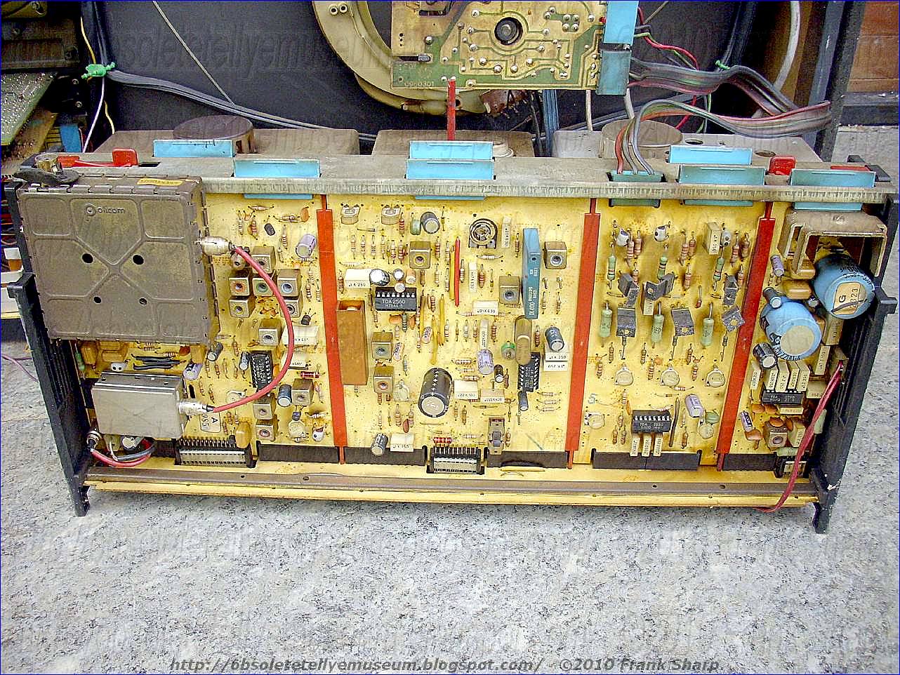
The SINUDYNE TELECOMPUTER 2658 THOR HIFI is a 26 inches color television with HIFI sound.
It has 16 programs and Infra red remote control, headphones jack and tone control.
Was first SINUDYNE model featuring PLL Synthesizer tuning system (ITT) and was first Italian color television set featuring first time the PLL Synthesizer tuning system, a frequency synthesizer controlled channel selection means which includes a fine tuning arrangement; means for initiating a sweep of available channels by the channel selection means; means for stopping the sweep on reception of a signal and means, operable on cessation of sweeping and responsive to the frequency of the signal, and arranged to control the fine tuning arrangement to compensate for frequency drift of the signal.
Television receivers of the type under consideration frequently include a frequency synthesizer for tuning the receiver's local oscillator to the nominal carrier frequency of a selected television channel. Generally, the frequency synthesizer compares the local oscillator frequency to a reference frequency associated with the selected channel, and then varies the local oscillator frequency until it equals the reference frequency. Presumably, the receiver will now be correctly tuned to the selected channel.
This method of tuning the receiver relies, of course, on the frequency of the incoming television signal being equal to its nominal or standard frequency. Such phase/frequency control circuits as preferably used for station selection in radio and television sets and are also referred to as "PLL systems" or "frequency synthesis systems". If used in radio and television sets, the voltage-controlled oscillator usually includes at least one varactor diode, to which the control voltage is applied to vary the capacitance and, hence, the frequency of the diode. In tuners working on the superhet principle, the voltage-controlled oscillator is the heterodyne oscillator.
 In accordance with the invention, a digital signal representative of the tuner local oscillator frequency is supplied to one input of a comparator with a digital signal representative of a desired channel number being supplied to the other input. The local oscillator frequency and, hence the system tuning, is varied in accordance with a correction signal which is dependent upon the state of the comparator. As a result of the desired channel number input, a driving ramp voltage is applied to the varactor and effectively results in a systematic channel-by-channel search for a predetermined acceptable region of frequencies about the desired channel frequency. The search is carried out at a very high speed, with a repetitive time sampling and comparison technique and, as far as the viewer is concerned, is practically instantaneous. The acceptance region is defined by a "window" which is made narrow enough to define the desired channel without adjacent channel interference, yet broad enough to permit minor deviations in carrier frequency without initiating corrective action.
In the preferred implementation of the invention, the tuning system incorporates a presettable modular scaler which drives presettable units and tens counters. Any base for the modular scaler may be chosen in conjunction with its preset information and the other counters and their preset information) to provide correct decoding of the oscillator frequency into the corresponding channel number regardless of its frequency band location. Thus, having a predetermined modulus (base), the modular scaler preset determines how many counts are required to provide a pulse to the units counter. The units counter functions in a similar manner to supply pulses to the tens counter. The base of the modular scaler is selected to produce a desired relationship for the intrachannel frequency spacing. Within the frequency window maintained by the tuning system, a normal automatic frequency control (AFC) in the receiver operates to lock the local oscillator frequency to the picture IF carrier. Since the tuning system operates on the local oscillator frequency, there is no dependence on individual characteristics of the varactor other than the requirement that the tuner drive system must be capable of tuning the varactor tuner over all channels.This invention relates to a digitally controlled, electronic tuner that can be tuned to any of several different channels at different frequencies and which includes an automatic fine tuning (AFT) circuit to adjust the tuning precisely when the frequency to which the tuner is tuned is within a predetermined frequency range close to the exact desired frequency. In particular, the invention relates to a television signal tuner for a receiver having an AFT circuit to maintain the tuning at a selected frequency according to one of the available channels and further including means to overcome the effect of the AFT circuit when it is desired to shift the tuner to a different channel.
 PLL SYNTHESIZED TUNING System Concepts:
INTRODUCTION Digital tuning systems are fast replacing the conventional mechanical systems in AM FM and television receivers The desirability of the digital approach is mainly due to the following features * Precise tuning of station frequencies
* Exact digital frequency display
* Keyboard entry of desired frequency
* Virtually unlimited station memory
* Up down scanning through the band
* Station ‘‘search’’ (stop on next active station)
* Power on to the last station
* Easy option for time-of-day clock In addition
" recent "developments in large scale integrated circuit technology and new varactor diodes for the AM band have made the cost-benefit picture for digital tuning very attractive System partitioning is extremely important in optimizing this cost-benefit picture as will be discussed.
SYSTEM DESCRIPTION
A simplified block diagram of a typical digitally tuned receiver is shown in Figure 1 Notice this receiver could be one for AM FM marine radio or television it makes no difference The frequency synthesizer block generates the local oscillator frequency for the receiver just as a conventional mechanical tuner would However the phase-locked-loop (PLL) acts as an integral frequency multiplier of an accurate crystal controlled reference frequency while the mechanical type provides a continuously variable frequency output with no reference Some method of controlling the value of the multiplier for channel tuning must be provided The other RF IF and audio video circuitry will be the same as in the mechanical tuning method There are many different ways to partition the frequency synthesizer system to perform the digital tuning function................
The set is a first in featuring a new set of PAL decoder chips which has been introduced by Siemens, the TDA2560/TDA2522/TDA2530. The first two of these second -source the latest Philips/Mullard decoder i.c.s, with the TDA2560 as luminance and chrominance signal amplifier and the TDA2522 as the reference oscillator/chrominance demodulator. Interesting features of this set up are the fact that the burst signal passes through the chrominance delay line and the fact that the reference oscillator operates at 8.86MHz, a digital divider providing exactly 90° phase displaced 4.43MHz outputs without the need for a phase shift coil. The first UK produced chassis to use these i.c.s is the Tandberg CTV3, the larger UK setmakers staying for the time being with the TBA560C/TBA540/TCA800 combination. The third i.c. from Siemens is the TDA2530 which supersedes the well known TBA530 luminance/colour-difference signal matrix- ing i.c. The TDA2530 contains a negative feedback driver amplifier and internal clamping in addition to the matrixing network.
And first SINUDYNE using the PHILIPS 30AX CRT TUBE.
The 30AX system, which Philips introduced in 1979, is an important landmark in the development of colour picture systems. With previous systems the assembly technician had to workthrough a large number of complicated setting-up procedures whenever he fitted a television picture tube with aset of coils for deflecting the electron beams. These procedures were necessary to ensure that the beams for the three colours would converge at thescreen for every deflection. They are no longer necessary with the 30AX system: for a given screen format any deflection unit can be combined with any tube to form a single 'dynamically convergent' unit. A colour-television receiver can thus be assembled from its components almost as easily as a monochrome receiver. The colour picture tube of the PHILIPS 30AX system displays a noticeably sharper picture over the entire screen surface. This will be particularly noticeable when data transmissions such as Viewdata and Teletext are displayed. This has been achieved by a reduction in the size of the beam spot by about 30%. Absence of coma and the retention of the 36.5 mm neck diameter have both contributed to increased picture sharpness. Coma has been eliminated by means of corrective field shapers embedded in the deflection coils which are sectionally wound saddle types. The new deflection unit has no rear flanges. enabling uniform self-convergence to be obtained for all screen sizes. without special corrections, adjustments, or tolerance compensations. Horizontal raster distortion is reduced and no vertical correction is required. One of the inventions in 30AX is an internal magnetic c orrection
system which obviates static convergence and colour purity errors.
This enables the usual multiple unit to be dispensed with. together
with the need for its adjustment ! New techniques have been employed
to achieve close tolerance construction of the glass envelope. In
addition, the 30AX picture tube incorporates two features whereby it
can be accurately adjusted during the last stages of manufacture. One
is the internal magnetic correction system. The other is an array of
bosses on the cone that establish a precise reference for the axial
purity positioning of the deflection unit on the tube axis and for
raster orientation. During its manufacture, each deflection unit is
individually adjusted for optimum convergence. The coil carrier also
incorporates reference bosses that co-operate with those on the cone of
the tube. ' Since every picture tube and every deflection unit is
individually pre-aligned, any deflection unit automatically matches
with any picture tube of the appropriate size. The deflection unit has
only to be pushed onto the neck of the tube unit it seats. Once the
reference bosses are engaged, the combination is accurately aligned and
requires no adjustment for convergence, colour purity or raster
orientation. With no multiple unit and a flangeless deflection unit,
there is more space in the receiver cabinet. Higher deflection
sensitivity means that less current is consumed, and consequently less
heat is produced. This increases the reliability of the TV receiver
again. 30AX means simple assembly. Any picture tube is compatible with
any deflection unit of the appropriate size and is automatically
self-aligning as well as being self-convergent.
orrection
system which obviates static convergence and colour purity errors.
This enables the usual multiple unit to be dispensed with. together
with the need for its adjustment ! New techniques have been employed
to achieve close tolerance construction of the glass envelope. In
addition, the 30AX picture tube incorporates two features whereby it
can be accurately adjusted during the last stages of manufacture. One
is the internal magnetic correction system. The other is an array of
bosses on the cone that establish a precise reference for the axial
purity positioning of the deflection unit on the tube axis and for
raster orientation. During its manufacture, each deflection unit is
individually adjusted for optimum convergence. The coil carrier also
incorporates reference bosses that co-operate with those on the cone of
the tube. ' Since every picture tube and every deflection unit is
individually pre-aligned, any deflection unit automatically matches
with any picture tube of the appropriate size. The deflection unit has
only to be pushed onto the neck of the tube unit it seats. Once the
reference bosses are engaged, the combination is accurately aligned and
requires no adjustment for convergence, colour purity or raster
orientation. With no multiple unit and a flangeless deflection unit,
there is more space in the receiver cabinet. Higher deflection
sensitivity means that less current is consumed, and consequently less
heat is produced. This increases the reliability of the TV receiver
again. 30AX means simple assembly. Any picture tube is compatible with
any deflection unit of the appropriate size and is automatically
self-aligning as well as being self-convergent.
The well-known 20AX features of HI-Bri, Soft-Flash and Quick-vision are maintained in the new 30AX systern. In their work on the design of deflection coils in the last few years the developers have expanded the magnetic deflectionfields into 'multipoles', This approach has improved the understanding of the relations between coil and field and between field and deflection to such an extent that designing deflection units is now more like playing a difficult but fascinating game of chess than carrying out the obscure computing procedure once necessary.Now that the new Philips 30AX tube has put in an appearance, some details can be filled in. The new tube has been developed from the 20AX, which has been in production since 1974, but brings with it several important advances. First, no dynamic convergence, static convergence, purity or raster correction adjustments are necessary. Secondly the new yoke design gives improved deflection sensitivity, a straight NS raster, and reduced EW raster distortion. Due to the close mechanical tolerances and the inclusion of positioning bosses on the tube bowl, the tube and yoke can be aligned simply by being pushed together - any 30AX yoke will automatically match any 30AX tube of the appropriate size. Thirdly the newly designed electron gun gives a sharper spot, with greater focus uniformity over the screen area. An internal magnetic ring is used to give correct purity and static beam convergence, in place of the multipole unit used in previous in -line gun tube designs. This results in a strikingly compact assembly. The automatic yoke/tube alignment does away with the need for preset mechanical tilt and shift adjustments which, Philips point out, correct one error by introducing another. The new tube is being produced in the 26, 22 and 20in. screen sizes. The power consumption of a set fitted with the 30AX is typicaly 100W compared to 120W with the 20AX system, at 1.2mA beam current and with an e.h.t. of 25kV. This compares with 88W for a set fitted with a 90° narrow -neck tube and hybrid yoke, under the same conditions.
Was featuring first time the PROFESSIONAL 2000 MO DULAR CHASSIS CONCEPT.
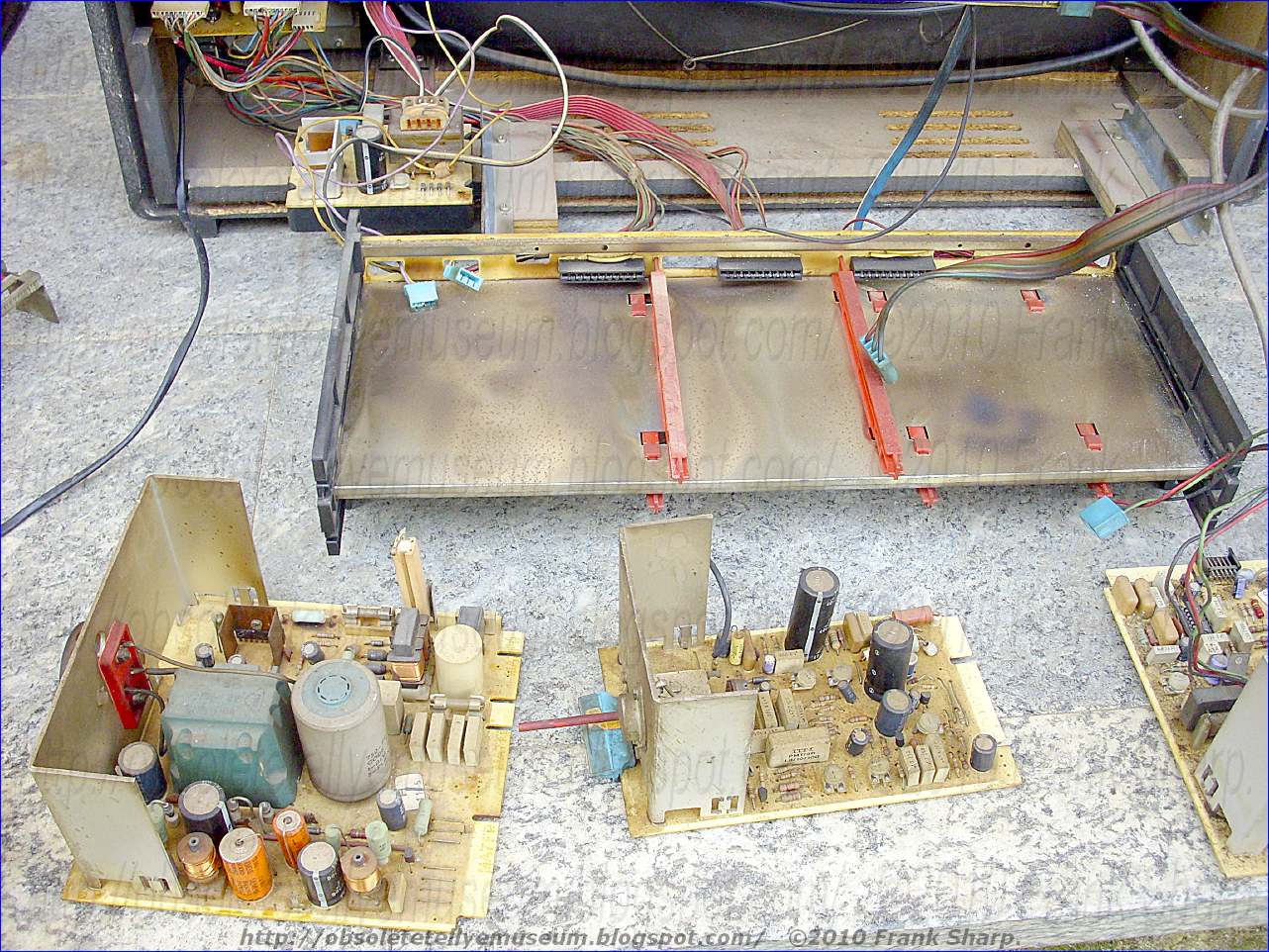
The television receiver also includes a wiring harness including a plurality of wires interconnecting the electronic chassis and picture tube within the cabinet. A plurality of connectors are positioned on the main electronic chassis and are interconnected by the wires within the wiring harness. A plurality of electronic modules are positioned within the electronic chassis with each of the modules having at least one connector thereon. The connectors on the electronic modules care placed so as to mate with the connectors mounted on the electronic chassis for interconnection between the electronic modules and the picture tube. By this means the various electronic modules can be removed by unplugging the connectors and without requiring soldering or unsoldering of any wires in the set.
Was first Sinudyne TV set featuring a Switching power supply based on SIemens TDA4600. Switching regulators serve as efficient and compact power supplies for instruments such as television receivers. A switching regulator may typically comprise a power transformer having a primary winding coupled to an input voltage source and to a power switch and a secondary winding coupled to a rectifier arrangement for developing a DC supply voltage for the instrument. A regulator control circuit generates pulse width modulated control signals that control the duty cycle of the power switch. A power switch is coupled to an inductance and a source of input voltage. A control circuit is coupled to the power switch for producing the switching thereof to transfer energy from the input voltage source to a load circuit coupled to the inductance. The control circuit is responsive to control voltages for varying the duty cycle of the power switch to control the transfer of energy to the load. A first control voltage representative of a variation in an energy level of the load circuit is developed to control the duty cycle in a manner that regulates the energy level.
It has a Transistorized horizontal deflection circuits made up of a horizontal switching or output transistor, a diode, one or more capacitors and a deflection winding. The output transistor, operating as a switch, is driven by a horizontal rate square wave signal and conducts during a portion of the horizontal trace interval. A diode, connected in parallel with the transistor, conducts during the remainder of the trace interval. A retrace capacitor and the deflection yoke winding are coupled in parallel across the transistor-diode combination. Energy is transferred into and out of the deflection winding via the diode and output transistor during the trace interval and via the retrace capacitor during the retrace interval.
In some television receivers, the collector of the horizontal output transistor is coupled to the B+ power supply through the primary windings of the high voltage transformer.
 IN general the set is build with a Modular chassis design because as modern television receivers become more complex the problem of repairing the receiver becomes more difficult. As the number of components used in the television receiver increases the susceptibility to breakdown increases and it becomes more difficult to replace defective components as they are more closely spaced. The problem has become even more complicated with the increasing number of color television receivers in use. A color television receiver has a larger number of circuits of a higher degree of complexity than the black and white receiver and further a more highly trained serviceman is required to properly service the color television receiver.
Fortunately for the service problem to date, most failures occur in the vacuum tubes used in the television receivers. A faulty or inoperative vacuum tube is relatively easy to find and replace. However, where the television receiver malfunction is caused by the failure of other components, such as resistors, capacitors or inductors, it is harder to isolate the defective component and a higher degree of skill on the part of the serviceman is required.
Even with the great majority of the color television receiver malfunctions being of the "easy to find and repair" type proper servicing of color sets has been difficult to obtain due to the shortage of trained serviceman.
At the present time advances in the state of the semiconductor art have led to the increasing use of transistors in color television receivers. The receiver described in this application has only two tubes, the picture tube and the high voltage rectifier tube, all the other active components in the receiver being semiconductors.
One important characteristic of a semiconductor device is its extreme reliability in comparison with the vacuum tube. The number of transistor and integrated circuit failures in the television receiver will be very low in comparison with the failures of other components, the reverse of what is true in present day color television receivers. Thus most failures in future television receivers will be of the hard to service type and will require more highly qualified servicemen.
The primary symptoms of a television receiver malfunction are shown on the picture tube of the television receiver while the components causing the malfunction are located within the cabinet. Also many adjustments to the receiver require the serviceman to observe the screen. Thus the serviceman must use unsatisfactory mirror arrangements to remove the electronic chassis from the cabinet, usually a very difficult task. Further many components are "buried" in a maze of circuitry and other components so that they are difficult to remove and replace without damage to other components in the receiver.
Repairing a modern color television receiver often requires that the receiver be removed from the home and carried to a repair shop where it may remain for many weeks. This is an expensive undertaking since most receivers are bulky and heavy enough to require at least two persons to carry them. Further, two trips must be made to the home, one to pick up the receiver and one to deliver it. For these reasons, the cost of maintaining the color television receiver in operating condition often exceeds the initial cost of the receiver and is an important factor in determining whether a receiver will be purchased.
Therefore, the object of this invention is to provide a transistorized color television receiver in which the main electronic chassis is easily accessible for maintenance and adjustment. Another object of this invention is to provide a transistorized color television receiver in which the electronic circuits are divided into a plurality of modules with the modules easily removable for service and maintenance. The main electronic chassis is slidably mounted within the cabinet so that it may be withdrawn, in the same manner as a drawer, to expose the electronic circuitry therein for maintenance and adjustment from the rear closure panel after easy removal. Another aspect is the capability to be serviced at eventually the home of the owner.
SINUDYNE was an Italian manufacturer of radio and television sets.
It was founded in 1946 SEI-Società Elettronica Italiana S.p.A., by two mates : Antonio Longhi and Bruno Berti, and they started manufacturing radio apparates with tubes.
In 1954 the started producing television sets which was in the 70's theyr primary activity.
In 1959 the production was transferred at Ozzano dell'Emilia near Bologna.
SINUDYNE have had a good success in Italy were it have had large diffusion and lots of service centers because a good quality of product and design.
In 1983 SINUDYNE realized the first Italian Digital Television employing the ITT DIGIVISION Technology
SINUDYNE was in the 1980's and in the 1990's even importer of brands like NORDMENDE and
ORION.
SINUDYNE was even known for it's product design which was quite remarcable some times.
The slogan of SINUDYNE in the 80's was "SINUDYNE COLORE STUPORE ! " and it was meaning " SINUDYNE COLOR ASTONISHMENT " in English.
In 2002 SINUDYNE was aquired by another Italian group called Merloni which introduced productions of appliances like air conditioning clima systems.
In 2003 SINUDYNE started marketing LCD (Crap) displays.
In 2006 SINUDYNE closed his production factory landing to fail !!
Redazione, la crisi, in La Repubblica - Sezione di Bologna, 1º settembre 2006, p. 2. URL consultato il 20 febbraio 2021.
Chi siamo 1946-1970, su sinudyne.com. URL consultato il 20 febbraio 2021 (archiviato dall'url originale il 5 maggio 2006).
Bruno Berti, su virtuspedia.it. URL consultato il 20 febbraio 2021.
^ 1950, su sinudyne.com. URL consultato il 20 febbraio 2021 (archiviato dall'url originale il 5 maggio 2006).
^ 1953, su sinudyne.com. URL consultato il 20 febbraio 2021 (archiviato dall'url originale il 5 maggio 2006).
Quale futuro per la tv Made in Italy?, in Trade Consumer Electronics, E2S, settembre 2006, p. 34.
^ 1954, su sinudyne.com. URL consultato il 20 febbraio 2021 (archiviato dall'url originale il 5 maggio 2006).
^ 1956, su sinudyne.com. URL consultato il 20 febbraio 2021 (archiviato dall'url originale il 5 maggio 2006).
R. Ferretti, L'industrializzazione: dalla comunità locale ai mercati mondiali, in Dalla guerra al "boom". Territorio, economia, società e politica nei comuni della pianura orientale bolognese. Industrializzazione e società. Economia, demografia e stili di vita, vol. 3, 2006, p. 177.
^ 1964, su sinudyne.com. URL consultato il 21 febbraio 2021 (archiviato dall'url originale il 5 maggio 2006).
^ 1969, su sinudyne.com. URL consultato il 21 febbraio 2021 (archiviato dall'url originale il 5 maggio 2006).
^ 1970, su sinudyne.com. URL consultato il 21 febbraio 2021 (archiviato dall'url originale il 5 maggio 2006).
^ 1975, su sinudyne.com. URL consultato il 21 febbraio 2021 (archiviato dall'url originale il 5 maggio 2006).
^ 1980, su sinudyne.com. URL consultato il 21 febbraio 2021 (archiviato dall'url originale il 5 maggio 2006).
^ R. Cominotti, S. Mariotti, Italia multinazionale 1990. L'integrazione internazionale e le prospettive del Mercato Unico Europeo. III rapporto R&P al CNEL, Franco Angeli, 1990, pp. 304, 421.
^ Sinudyne, Societá Elettronica Italiana, su radiomuseum.org. URL consultato il 6 luglio 2022 (archiviato il 1º luglio 2018).
^ 1983, su sinudyne.com. URL consultato il 21 febbraio 2021 (archiviato dall'url originale il 5 maggio 2006).
^ Redazione, S.E.I. Sinudyne: il marchio Orion sarà distribuito da Euronics, in E-Duesse.it, 1º maggio 2009. URL consultato il 6 luglio 2022 (archiviato il 6 luglio 2022).
^ 1992, su sinudyne.com. URL consultato il 21 febbraio 2021 (archiviato dall'url originale il 5 maggio 2006).
^ 1993-2002, su sinudyne.com. URL consultato il 21 febbraio 2021 (archiviato dall'url originale il 5 maggio 2006).
^ 1996, su sinudyne.com. URL consultato il 21 febbraio 2021 (archiviato dall'url originale il 5 maggio 2006).
^ 1997, su sinudyne.com. URL consultato il 21 febbraio 2021 (archiviato dall'url originale il 5 maggio 2006).
^ 1998, su sinudyne.com. URL consultato il 21 febbraio 2021 (archiviato dall'url originale il 5 maggio 2006).
^ 1999, su sinudyne.com. URL consultato il 21 febbraio 2021 (archiviato dall'url originale il 5 maggio 2006).
^ (ES) Audiotecnic, televisores para todo el mundo, in Laesfera, 21 dicembre 2003. URL consultato il 21 febbraio 2021 (archiviato dall'url originale il 27 dicembre 2009).
^ (ES) La plantilla de Audiotecnic (antigua Thomson) se concentra en San Sebastián de los Reyes (Madrid), en defensa de sus empleos, in ANIA, 16 novembre 2004. URL consultato il 21 febbraio 2021.
^ 2000, su sinudyne.com. URL consultato il 21 febbraio 2021 (archiviato dall'url originale il 5 maggio 2006).
^ Redazione, Sinudyne: l'azienda acquisita da Panini, in E-Duesse.it, 1º maggio 2009. URL consultato il 6 luglio 2022 (archiviato il 6 luglio 2022).
^ Redazione, EICMA: BERTI, MOTO MORINI SI RISVEGLIA, in Motor Press, 17 novembre 2005. URL consultato il 6 luglio 2022 (archiviato il 28 luglio 2021).
^ L. Nigro, Rinasce un marchio storico torna la Moto Morini, in La Repubblica - Sezione di Bologna, 5 dicembre 2003, p. 5. URL consultato il 6 luglio 2022 (archiviato l'11 agosto 2018).
^ Synudine vuole licenziare 83 dipendenti, in L'Unità, 25 giugno 2005, p. 14.
^ Fineldo, lo scrigno di famiglia che ha fatto il peno di utili, in La Repubblica, 12 novembre 2007, p. 19. URL consultato il 6 luglio 2022 (archiviato l'8 marzo 2013).
^ Redazione, SINUDYNE: L'AZIENDA ACQUISITA DA PANINI, in E-Duesse.it, 9 aprile 2003. URL consultato il 21 febbraio 2021.
^ Storia 2003, su sinudyne.com. URL consultato il 21 febbraio 2021 (archiviato dall'url originale il 5 maggio 2006).
^ Duesse Communication S.r.l., Sinudyne: in arrivo il televisore con combinato Dvd+Vhs, in E2S, 19 novembre 2002. URL consultato il 6 luglio 2022 (archiviato il 6 luglio 2022).
^ Lamberto Angelini, in Ottagono, n. 174, Editrice Co.P.IN.A, ottobre 2004, p. 174.
^ Product, su angelinidesign.eu. URL consultato il 21 febbraio 2021.
^ Redazione, Merloni Progetti: nasce la linea ped a marchio Sinudyne, in E-Duesse.it, 1º maggio 2009. URL consultato il 6 luglio 2022 (archiviato il 6 luglio 2022).
^ Redazione, Sinudyne: delocalizzata in Lituania la produzione di Crt e Lcd, in E-Duesse.it, 1º maggio 2009. URL consultato il 6 luglio 2022 (archiviato il 6 luglio 2022).
^ F. Allegra, Merloni e Mister Panini cercano un socio cinese per i televisori Sinudyne, in Milano Finanza, n. 181, 14 settembre 2005, p. 10.
^ Redazione, MERLONI PROGETTI: JOINT VENTURE CON JOYCARE, in E-Duesse.it, 21 febbraio 2006. URL consultato il 21 febbraio 2021.
Redazione, Sinudyne: l'azienda chiude, in E-Duesse.it, 1º maggio 2009. URL consultato il 6 luglio 2022 (archiviato il 6 luglio 2022). ^ Sinudyne: l'azienda chiude. Accordo per mobilità lavoratori, in Sassuolo 2000. URL consultato il 6 luglio 2022 (archiviato dall'url originale il 23 settembre 2020). ^ Capannoni ex Sinudyne di Ozzano demoliti entro 2 mesi | Sabato Sera, su sabatosera.it, 2 marzo 2021. URL consultato il 6 luglio 2022 (archiviato il 6 luglio 2022). ^ Iniziati i lavori di abbattimento dei capannoni dell'ex Sinudyne. | Comune di Ozzano dell'Emilia, su comune.ozzano.bo.it. URL consultato il 6 luglio 2022 (archiviato il 19 giugno 2022). ^ Ditte anni 60, su carlobramantiradio.it. URL consultato il 6 luglio 2022 (archiviato il 6 luglio 2022). ^ Sinudyne, su virtuspedia.it. URL consultato il 6 luglio 2022 (archiviato il 25 aprile 2022). ^ La Virtus Sinudyne vince il campionato di basket, 4 aprile 1976, su bibliotecasalaborsa.it. URL consultato il 13 gennaio 2023. ^ M. Bertuzzi, F. Monti, La maglia del Bologna. Storia delle divise rossoblù, Edizioni Minerva, 2017, pp. 156-159.
It has 16 programs and Infra red remote control, headphones jack and tone control.
Was first SINUDYNE model featuring PLL Synthesizer tuning system (ITT) and was first Italian color television set featuring first time the PLL Synthesizer tuning system, a frequency synthesizer controlled channel selection means which includes a fine tuning arrangement; means for initiating a sweep of available channels by the channel selection means; means for stopping the sweep on reception of a signal and means, operable on cessation of sweeping and responsive to the frequency of the signal, and arranged to control the fine tuning arrangement to compensate for frequency drift of the signal.
Television receivers of the type under consideration frequently include a frequency synthesizer for tuning the receiver's local oscillator to the nominal carrier frequency of a selected television channel. Generally, the frequency synthesizer compares the local oscillator frequency to a reference frequency associated with the selected channel, and then varies the local oscillator frequency until it equals the reference frequency. Presumably, the receiver will now be correctly tuned to the selected channel.
This method of tuning the receiver relies, of course, on the frequency of the incoming television signal being equal to its nominal or standard frequency. Such phase/frequency control circuits as preferably used for station selection in radio and television sets and are also referred to as "PLL systems" or "frequency synthesis systems". If used in radio and television sets, the voltage-controlled oscillator usually includes at least one varactor diode, to which the control voltage is applied to vary the capacitance and, hence, the frequency of the diode. In tuners working on the superhet principle, the voltage-controlled oscillator is the heterodyne oscillator.
In accordance with the invention, a digital signal representative of the tuner local oscillator frequency is supplied to one input of a comparator with a digital signal representative of a desired channel number being supplied to the other input. The local oscillator frequency and, hence the system tuning, is varied in accordance with a correction signal which is dependent upon the state of the comparator. As a result of the desired channel number input, a driving ramp voltage is applied to the varactor and effectively results in a systematic channel-by-channel search for a predetermined acceptable region of frequencies about the desired channel frequency. The search is carried out at a very high speed, with a repetitive time sampling and comparison technique and, as far as the viewer is concerned, is practically instantaneous. The acceptance region is defined by a "window" which is made narrow enough to define the desired channel without adjacent channel interference, yet broad enough to permit minor deviations in carrier frequency without initiating corrective action. In the preferred implementation of the invention, the tuning system incorporates a presettable modular scaler which drives presettable units and tens counters. Any base for the modular scaler may be chosen in conjunction with its preset information and the other counters and their preset information) to provide correct decoding of the oscillator frequency into the corresponding channel number regardless of its frequency band location. Thus, having a predetermined modulus (base), the modular scaler preset determines how many counts are required to provide a pulse to the units counter. The units counter functions in a similar manner to supply pulses to the tens counter. The base of the modular scaler is selected to produce a desired relationship for the intrachannel frequency spacing. Within the frequency window maintained by the tuning system, a normal automatic frequency control (AFC) in the receiver operates to lock the local oscillator frequency to the picture IF carrier. Since the tuning system operates on the local oscillator frequency, there is no dependence on individual characteristics of the varactor other than the requirement that the tuner drive system must be capable of tuning the varactor tuner over all channels.This invention relates to a digitally controlled, electronic tuner that can be tuned to any of several different channels at different frequencies and which includes an automatic fine tuning (AFT) circuit to adjust the tuning precisely when the frequency to which the tuner is tuned is within a predetermined frequency range close to the exact desired frequency. In particular, the invention relates to a television signal tuner for a receiver having an AFT circuit to maintain the tuning at a selected frequency according to one of the available channels and further including means to overcome the effect of the AFT circuit when it is desired to shift the tuner to a different channel.

INTRODUCTION Digital tuning systems are fast replacing the conventional mechanical systems in AM FM and television receivers The desirability of the digital approach is mainly due to the following features * Precise tuning of station frequencies
* Exact digital frequency display
* Keyboard entry of desired frequency
* Virtually unlimited station memory
* Up down scanning through the band
* Station ‘‘search’’ (stop on next active station)
* Power on to the last station
* Easy option for time-of-day clock In addition
" recent "developments in large scale integrated circuit technology and new varactor diodes for the AM band have made the cost-benefit picture for digital tuning very attractive System partitioning is extremely important in optimizing this cost-benefit picture as will be discussed.
SYSTEM DESCRIPTION
A simplified block diagram of a typical digitally tuned receiver is shown in Figure 1 Notice this receiver could be one for AM FM marine radio or television it makes no difference The frequency synthesizer block generates the local oscillator frequency for the receiver just as a conventional mechanical tuner would However the phase-locked-loop (PLL) acts as an integral frequency multiplier of an accurate crystal controlled reference frequency while the mechanical type provides a continuously variable frequency output with no reference Some method of controlling the value of the multiplier for channel tuning must be provided The other RF IF and audio video circuitry will be the same as in the mechanical tuning method There are many different ways to partition the frequency synthesizer system to perform the digital tuning function................
The set is a first in featuring a new set of PAL decoder chips which has been introduced by Siemens, the TDA2560/TDA2522/TDA2530. The first two of these second -source the latest Philips/Mullard decoder i.c.s, with the TDA2560 as luminance and chrominance signal amplifier and the TDA2522 as the reference oscillator/chrominance demodulator. Interesting features of this set up are the fact that the burst signal passes through the chrominance delay line and the fact that the reference oscillator operates at 8.86MHz, a digital divider providing exactly 90° phase displaced 4.43MHz outputs without the need for a phase shift coil. The first UK produced chassis to use these i.c.s is the Tandberg CTV3, the larger UK setmakers staying for the time being with the TBA560C/TBA540/TCA800 combination. The third i.c. from Siemens is the TDA2530 which supersedes the well known TBA530 luminance/colour-difference signal matrix- ing i.c. The TDA2530 contains a negative feedback driver amplifier and internal clamping in addition to the matrixing network.
And first SINUDYNE using the PHILIPS 30AX CRT TUBE.
The 30AX system, which Philips introduced in 1979, is an important landmark in the development of colour picture systems. With previous systems the assembly technician had to workthrough a large number of complicated setting-up procedures whenever he fitted a television picture tube with aset of coils for deflecting the electron beams. These procedures were necessary to ensure that the beams for the three colours would converge at thescreen for every deflection. They are no longer necessary with the 30AX system: for a given screen format any deflection unit can be combined with any tube to form a single 'dynamically convergent' unit. A colour-television receiver can thus be assembled from its components almost as easily as a monochrome receiver. The colour picture tube of the PHILIPS 30AX system displays a noticeably sharper picture over the entire screen surface. This will be particularly noticeable when data transmissions such as Viewdata and Teletext are displayed. This has been achieved by a reduction in the size of the beam spot by about 30%. Absence of coma and the retention of the 36.5 mm neck diameter have both contributed to increased picture sharpness. Coma has been eliminated by means of corrective field shapers embedded in the deflection coils which are sectionally wound saddle types. The new deflection unit has no rear flanges. enabling uniform self-convergence to be obtained for all screen sizes. without special corrections, adjustments, or tolerance compensations. Horizontal raster distortion is reduced and no vertical correction is required. One of the inventions in 30AX is an internal magnetic c
 orrection
system which obviates static convergence and colour purity errors.
This enables the usual multiple unit to be dispensed with. together
with the need for its adjustment ! New techniques have been employed
to achieve close tolerance construction of the glass envelope. In
addition, the 30AX picture tube incorporates two features whereby it
can be accurately adjusted during the last stages of manufacture. One
is the internal magnetic correction system. The other is an array of
bosses on the cone that establish a precise reference for the axial
purity positioning of the deflection unit on the tube axis and for
raster orientation. During its manufacture, each deflection unit is
individually adjusted for optimum convergence. The coil carrier also
incorporates reference bosses that co-operate with those on the cone of
the tube. ' Since every picture tube and every deflection unit is
individually pre-aligned, any deflection unit automatically matches
with any picture tube of the appropriate size. The deflection unit has
only to be pushed onto the neck of the tube unit it seats. Once the
reference bosses are engaged, the combination is accurately aligned and
requires no adjustment for convergence, colour purity or raster
orientation. With no multiple unit and a flangeless deflection unit,
there is more space in the receiver cabinet. Higher deflection
sensitivity means that less current is consumed, and consequently less
heat is produced. This increases the reliability of the TV receiver
again. 30AX means simple assembly. Any picture tube is compatible with
any deflection unit of the appropriate size and is automatically
self-aligning as well as being self-convergent.
orrection
system which obviates static convergence and colour purity errors.
This enables the usual multiple unit to be dispensed with. together
with the need for its adjustment ! New techniques have been employed
to achieve close tolerance construction of the glass envelope. In
addition, the 30AX picture tube incorporates two features whereby it
can be accurately adjusted during the last stages of manufacture. One
is the internal magnetic correction system. The other is an array of
bosses on the cone that establish a precise reference for the axial
purity positioning of the deflection unit on the tube axis and for
raster orientation. During its manufacture, each deflection unit is
individually adjusted for optimum convergence. The coil carrier also
incorporates reference bosses that co-operate with those on the cone of
the tube. ' Since every picture tube and every deflection unit is
individually pre-aligned, any deflection unit automatically matches
with any picture tube of the appropriate size. The deflection unit has
only to be pushed onto the neck of the tube unit it seats. Once the
reference bosses are engaged, the combination is accurately aligned and
requires no adjustment for convergence, colour purity or raster
orientation. With no multiple unit and a flangeless deflection unit,
there is more space in the receiver cabinet. Higher deflection
sensitivity means that less current is consumed, and consequently less
heat is produced. This increases the reliability of the TV receiver
again. 30AX means simple assembly. Any picture tube is compatible with
any deflection unit of the appropriate size and is automatically
self-aligning as well as being self-convergent.
The well-known 20AX features of HI-Bri, Soft-Flash and Quick-vision are maintained in the new 30AX systern. In their work on the design of deflection coils in the last few years the developers have expanded the magnetic deflectionfields into 'multipoles', This approach has improved the understanding of the relations between coil and field and between field and deflection to such an extent that designing deflection units is now more like playing a difficult but fascinating game of chess than carrying out the obscure computing procedure once necessary.Now that the new Philips 30AX tube has put in an appearance, some details can be filled in. The new tube has been developed from the 20AX, which has been in production since 1974, but brings with it several important advances. First, no dynamic convergence, static convergence, purity or raster correction adjustments are necessary. Secondly the new yoke design gives improved deflection sensitivity, a straight NS raster, and reduced EW raster distortion. Due to the close mechanical tolerances and the inclusion of positioning bosses on the tube bowl, the tube and yoke can be aligned simply by being pushed together - any 30AX yoke will automatically match any 30AX tube of the appropriate size. Thirdly the newly designed electron gun gives a sharper spot, with greater focus uniformity over the screen area. An internal magnetic ring is used to give correct purity and static beam convergence, in place of the multipole unit used in previous in -line gun tube designs. This results in a strikingly compact assembly. The automatic yoke/tube alignment does away with the need for preset mechanical tilt and shift adjustments which, Philips point out, correct one error by introducing another. The new tube is being produced in the 26, 22 and 20in. screen sizes. The power consumption of a set fitted with the 30AX is typicaly 100W compared to 120W with the 20AX system, at 1.2mA beam current and with an e.h.t. of 25kV. This compares with 88W for a set fitted with a 90° narrow -neck tube and hybrid yoke, under the same conditions.
Was featuring first time the PROFESSIONAL 2000 MO
 DULAR CHASSIS CONCEPT.
The television receiver also includes a wiring harness including a plurality of wires interconnecting the electronic chassis and picture tube within the cabinet. A plurality of connectors are positioned on the main electronic chassis and are interconnected by the wires within the wiring harness. A plurality of electronic modules are positioned within the electronic chassis with each of the modules having at least one connector thereon. The connectors on the electronic modules care placed so as to mate with the connectors mounted on the electronic chassis for interconnection between the electronic modules and the picture tube. By this means the various electronic modules can be removed by unplugging the connectors and without requiring soldering or unsoldering of any wires in the set.
Was first Sinudyne TV set featuring a Switching power supply based on SIemens TDA4600. Switching regulators serve as efficient and compact power supplies for instruments such as television receivers. A switching regulator may typically comprise a power transformer having a primary winding coupled to an input voltage source and to a power switch and a secondary winding coupled to a rectifier arrangement for developing a DC supply voltage for the instrument. A regulator control circuit generates pulse width modulated control signals that control the duty cycle of the power switch. A power switch is coupled to an inductance and a source of input voltage. A control circuit is coupled to the power switch for producing the switching thereof to transfer energy from the input voltage source to a load circuit coupled to the inductance. The control circuit is responsive to control voltages for varying the duty cycle of the power switch to control the transfer of energy to the load. A first control voltage representative of a variation in an energy level of the load circuit is developed to control the duty cycle in a manner that regulates the energy level.
It has a Transistorized horizontal deflection circuits made up of a horizontal switching or output transistor, a diode, one or more capacitors and a deflection winding. The output transistor, operating as a switch, is driven by a horizontal rate square wave signal and conducts during a portion of the horizontal trace interval. A diode, connected in parallel with the transistor, conducts during the remainder of the trace interval. A retrace capacitor and the deflection yoke winding are coupled in parallel across the transistor-diode combination. Energy is transferred into and out of the deflection winding via the diode and output transistor during the trace interval and via the retrace capacitor during the retrace interval.
In some television receivers, the collector of the horizontal output transistor is coupled to the B+ power supply through the primary windings of the high voltage transformer.
Fortunately for the service problem to date, most failures occur in the vacuum tubes used in the television receivers. A faulty or inoperative vacuum tube is relatively easy to find and replace. However, where the television receiver malfunction is caused by the failure of other components, such as resistors, capacitors or inductors, it is harder to isolate the defective component and a higher degree of skill on the part of the serviceman is required.
Even with the great majority of the color television receiver malfunctions being of the "easy to find and repair" type proper servicing of color sets has been difficult to obtain due to the shortage of trained serviceman.
At the present time advances in the state of the semiconductor art have led to the increasing use of transistors in color television receivers. The receiver described in this application has only two tubes, the picture tube and the high voltage rectifier tube, all the other active components in the receiver being semiconductors.
One important characteristic of a semiconductor device is its extreme reliability in comparison with the vacuum tube. The number of transistor and integrated circuit failures in the television receiver will be very low in comparison with the failures of other components, the reverse of what is true in present day color television receivers. Thus most failures in future television receivers will be of the hard to service type and will require more highly qualified servicemen.
The primary symptoms of a television receiver malfunction are shown on the picture tube of the television receiver while the components causing the malfunction are located within the cabinet. Also many adjustments to the receiver require the serviceman to observe the screen. Thus the serviceman must use unsatisfactory mirror arrangements to remove the electronic chassis from the cabinet, usually a very difficult task. Further many components are "buried" in a maze of circuitry and other components so that they are difficult to remove and replace without damage to other components in the receiver.
Repairing a modern color television receiver often requires that the receiver be removed from the home and carried to a repair shop where it may remain for many weeks. This is an expensive undertaking since most receivers are bulky and heavy enough to require at least two persons to carry them. Further, two trips must be made to the home, one to pick up the receiver and one to deliver it. For these reasons, the cost of maintaining the color television receiver in operating condition often exceeds the initial cost of the receiver and is an important factor in determining whether a receiver will be purchased.
Therefore, the object of this invention is to provide a transistorized color television receiver in which the main electronic chassis is easily accessible for maintenance and adjustment. Another object of this invention is to provide a transistorized color television receiver in which the electronic circuits are divided into a plurality of modules with the modules easily removable for service and maintenance. The main electronic chassis is slidably mounted within the cabinet so that it may be withdrawn, in the same manner as a drawer, to expose the electronic circuitry therein for maintenance and adjustment from the rear closure panel after easy removal. Another aspect is the capability to be serviced at eventually the home of the owner.
SINUDYNE was an Italian manufacturer of radio and television sets.
It was founded in 1946 SEI-Società Elettronica Italiana S.p.A., by two mates : Antonio Longhi and Bruno Berti, and they started manufacturing radio apparates with tubes.
In 1954 the started producing television sets which was in the 70's theyr primary activity.
In 1959 the production was transferred at Ozzano dell'Emilia near Bologna.
SINUDYNE have had a good success in Italy were it have had large diffusion and lots of service centers because a good quality of product and design.
In 1983 SINUDYNE realized the first Italian Digital Television employing the ITT DIGIVISION Technology
SINUDYNE was in the 1980's and in the 1990's even importer of brands like NORDMENDE and
ORION.
SINUDYNE was even known for it's product design which was quite remarcable some times.
The slogan of SINUDYNE in the 80's was "SINUDYNE COLORE STUPORE ! " and it was meaning " SINUDYNE COLOR ASTONISHMENT " in English.
In 2002 SINUDYNE was aquired by another Italian group called Merloni which introduced productions of appliances like air conditioning clima systems.
In 2003 SINUDYNE started marketing LCD (Crap) displays.
In 2006 SINUDYNE closed his production factory landing to fail !!
TODAY'S SINUDYNE IS NO MORE .................. DEAD !
Further readings and more Notes:
- ^ Sinudyne.com
^ fonte http://www.angelinidesign.eu/ e catalogo Sinudyne 2004)
^ Sinudyne.com
^ Sinudyne :: Virtuspedia, su www.virtuspedia.it. URL consultato il 22 agosto 2018.
^ Biblioteca Salaborsa, homepage, su Biblioteca salaborsa. URL consultato il 22 agosto 2018.
^ Articolo sullo stabilimento spagnolo Sinudyne Archiviato il 27 dicembre 2009 in Internet Archive.
^ schede tecniche[collegamento interrotto]
^ History of the radio manufacturer Sinudyne - Bologna, Radiomuseum.org. URL consultato il 1º luglio 2018 (archiviato dall'url originale il 31 gennaio 2015).
^ (IT) Duesse Communication S.r.l., Sinudyne: in arrivo il televisore con combinato Dvd+Vhs, in E2S. URL consultato il 22 agosto 2018.
- pag. 34 della rivista Trade Consumer Electronics del Settembre 2006
- ^ Merloni e Mister Panini cercano un socio cinese per i televisori Sinudyne - MilanoFinanza.it, su www.milanofinanza.it. URL consultato il 22 agosto 2018.
- ^ (IT) Duesse Communication S.r.l., Sinudyne: l’azienda chiude, in Editoriale Duesse. URL consultato il 22 agosto 2018.
- ^ (IT) Sinudyne: l’azienda chiude. Accordo per mobilità lavoratori, in Sassuolo 2000. URL consultato il 22 agosto 2018.
^ (IT) Duesse Communication S.r.l., Sinudyne: delocalizzata in Lituania la produzione di Crt e Lcd, in E2S. URL consultato il 22 agosto 2018.
Redazione, la crisi, in La Repubblica - Sezione di Bologna, 1º settembre 2006, p. 2. URL consultato il 20 febbraio 2021.
Chi siamo 1946-1970, su sinudyne.com. URL consultato il 20 febbraio 2021 (archiviato dall'url originale il 5 maggio 2006).
Bruno Berti, su virtuspedia.it. URL consultato il 20 febbraio 2021.
^ 1950, su sinudyne.com. URL consultato il 20 febbraio 2021 (archiviato dall'url originale il 5 maggio 2006).
^ 1953, su sinudyne.com. URL consultato il 20 febbraio 2021 (archiviato dall'url originale il 5 maggio 2006).
Quale futuro per la tv Made in Italy?, in Trade Consumer Electronics, E2S, settembre 2006, p. 34.
^ 1954, su sinudyne.com. URL consultato il 20 febbraio 2021 (archiviato dall'url originale il 5 maggio 2006).
^ 1956, su sinudyne.com. URL consultato il 20 febbraio 2021 (archiviato dall'url originale il 5 maggio 2006).
R. Ferretti, L'industrializzazione: dalla comunità locale ai mercati mondiali, in Dalla guerra al "boom". Territorio, economia, società e politica nei comuni della pianura orientale bolognese. Industrializzazione e società. Economia, demografia e stili di vita, vol. 3, 2006, p. 177.
^ 1964, su sinudyne.com. URL consultato il 21 febbraio 2021 (archiviato dall'url originale il 5 maggio 2006).
^ 1969, su sinudyne.com. URL consultato il 21 febbraio 2021 (archiviato dall'url originale il 5 maggio 2006).
^ 1970, su sinudyne.com. URL consultato il 21 febbraio 2021 (archiviato dall'url originale il 5 maggio 2006).
^ 1975, su sinudyne.com. URL consultato il 21 febbraio 2021 (archiviato dall'url originale il 5 maggio 2006).
^ 1980, su sinudyne.com. URL consultato il 21 febbraio 2021 (archiviato dall'url originale il 5 maggio 2006).
^ R. Cominotti, S. Mariotti, Italia multinazionale 1990. L'integrazione internazionale e le prospettive del Mercato Unico Europeo. III rapporto R&P al CNEL, Franco Angeli, 1990, pp. 304, 421.
^ Sinudyne, Societá Elettronica Italiana, su radiomuseum.org. URL consultato il 6 luglio 2022 (archiviato il 1º luglio 2018).
^ 1983, su sinudyne.com. URL consultato il 21 febbraio 2021 (archiviato dall'url originale il 5 maggio 2006).
^ Redazione, S.E.I. Sinudyne: il marchio Orion sarà distribuito da Euronics, in E-Duesse.it, 1º maggio 2009. URL consultato il 6 luglio 2022 (archiviato il 6 luglio 2022).
^ 1992, su sinudyne.com. URL consultato il 21 febbraio 2021 (archiviato dall'url originale il 5 maggio 2006).
^ 1993-2002, su sinudyne.com. URL consultato il 21 febbraio 2021 (archiviato dall'url originale il 5 maggio 2006).
^ 1996, su sinudyne.com. URL consultato il 21 febbraio 2021 (archiviato dall'url originale il 5 maggio 2006).
^ 1997, su sinudyne.com. URL consultato il 21 febbraio 2021 (archiviato dall'url originale il 5 maggio 2006).
^ 1998, su sinudyne.com. URL consultato il 21 febbraio 2021 (archiviato dall'url originale il 5 maggio 2006).
^ 1999, su sinudyne.com. URL consultato il 21 febbraio 2021 (archiviato dall'url originale il 5 maggio 2006).
^ (ES) Audiotecnic, televisores para todo el mundo, in Laesfera, 21 dicembre 2003. URL consultato il 21 febbraio 2021 (archiviato dall'url originale il 27 dicembre 2009).
^ (ES) La plantilla de Audiotecnic (antigua Thomson) se concentra en San Sebastián de los Reyes (Madrid), en defensa de sus empleos, in ANIA, 16 novembre 2004. URL consultato il 21 febbraio 2021.
^ 2000, su sinudyne.com. URL consultato il 21 febbraio 2021 (archiviato dall'url originale il 5 maggio 2006).
^ Redazione, Sinudyne: l'azienda acquisita da Panini, in E-Duesse.it, 1º maggio 2009. URL consultato il 6 luglio 2022 (archiviato il 6 luglio 2022).
^ Redazione, EICMA: BERTI, MOTO MORINI SI RISVEGLIA, in Motor Press, 17 novembre 2005. URL consultato il 6 luglio 2022 (archiviato il 28 luglio 2021).
^ L. Nigro, Rinasce un marchio storico torna la Moto Morini, in La Repubblica - Sezione di Bologna, 5 dicembre 2003, p. 5. URL consultato il 6 luglio 2022 (archiviato l'11 agosto 2018).
^ Synudine vuole licenziare 83 dipendenti, in L'Unità, 25 giugno 2005, p. 14.
^ Fineldo, lo scrigno di famiglia che ha fatto il peno di utili, in La Repubblica, 12 novembre 2007, p. 19. URL consultato il 6 luglio 2022 (archiviato l'8 marzo 2013).
^ Redazione, SINUDYNE: L'AZIENDA ACQUISITA DA PANINI, in E-Duesse.it, 9 aprile 2003. URL consultato il 21 febbraio 2021.
^ Storia 2003, su sinudyne.com. URL consultato il 21 febbraio 2021 (archiviato dall'url originale il 5 maggio 2006).
^ Duesse Communication S.r.l., Sinudyne: in arrivo il televisore con combinato Dvd+Vhs, in E2S, 19 novembre 2002. URL consultato il 6 luglio 2022 (archiviato il 6 luglio 2022).
^ Lamberto Angelini, in Ottagono, n. 174, Editrice Co.P.IN.A, ottobre 2004, p. 174.
^ Product, su angelinidesign.eu. URL consultato il 21 febbraio 2021.
^ Redazione, Merloni Progetti: nasce la linea ped a marchio Sinudyne, in E-Duesse.it, 1º maggio 2009. URL consultato il 6 luglio 2022 (archiviato il 6 luglio 2022).
^ Redazione, Sinudyne: delocalizzata in Lituania la produzione di Crt e Lcd, in E-Duesse.it, 1º maggio 2009. URL consultato il 6 luglio 2022 (archiviato il 6 luglio 2022).
^ F. Allegra, Merloni e Mister Panini cercano un socio cinese per i televisori Sinudyne, in Milano Finanza, n. 181, 14 settembre 2005, p. 10.
^ Redazione, MERLONI PROGETTI: JOINT VENTURE CON JOYCARE, in E-Duesse.it, 21 febbraio 2006. URL consultato il 21 febbraio 2021.
Redazione, Sinudyne: l'azienda chiude, in E-Duesse.it, 1º maggio 2009. URL consultato il 6 luglio 2022 (archiviato il 6 luglio 2022). ^ Sinudyne: l'azienda chiude. Accordo per mobilità lavoratori, in Sassuolo 2000. URL consultato il 6 luglio 2022 (archiviato dall'url originale il 23 settembre 2020). ^ Capannoni ex Sinudyne di Ozzano demoliti entro 2 mesi | Sabato Sera, su sabatosera.it, 2 marzo 2021. URL consultato il 6 luglio 2022 (archiviato il 6 luglio 2022). ^ Iniziati i lavori di abbattimento dei capannoni dell'ex Sinudyne. | Comune di Ozzano dell'Emilia, su comune.ozzano.bo.it. URL consultato il 6 luglio 2022 (archiviato il 19 giugno 2022). ^ Ditte anni 60, su carlobramantiradio.it. URL consultato il 6 luglio 2022 (archiviato il 6 luglio 2022). ^ Sinudyne, su virtuspedia.it. URL consultato il 6 luglio 2022 (archiviato il 25 aprile 2022). ^ La Virtus Sinudyne vince il campionato di basket, 4 aprile 1976, su bibliotecasalaborsa.it. URL consultato il 13 gennaio 2023. ^ M. Bertuzzi, F. Monti, La maglia del Bologna. Storia delle divise rossoblù, Edizioni Minerva, 2017, pp. 156-159.