


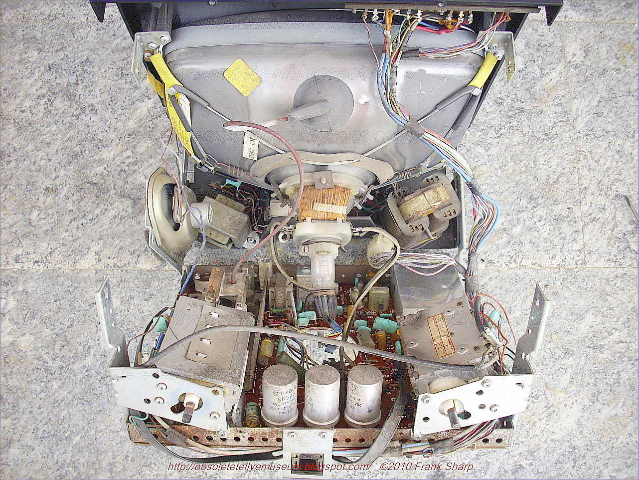
The chassis is realized on a monocarrier completely based around discretes semiconductors.
All semiconductors circuits were made by:ates and PHILIPS.
SGS is Società Generale Semiconduttori - Aquila Tubi E Semiconduttori (SGS-ATES, "Semiconductor General Society - Tubes and Semiconductors Aquila"), later SGS Microelettronica, a former Italian company now merged into STMicroelectronics
SGS
Microelettronica and Thomson Semiconducteurs were both
long-established semiconductor companies. SGS Microelettronica
originated in 1972 from a previous merger of two companies:
- ATES (Aquila Tubi e Semiconduttori), a vacuum tube and semiconductor maker headquartered in the Abruzzese city of l'Aquila, who in 1961 changed its name into Azienda Tecnica ed Elettronica del Sud and relocated its manufacturing plant in the outskirts of the Sicilian city of Catania
- Società Generale Semiconduttori (founded in 1957 by Adriano Olivetti).
 GENERAL BASIC TRANSISTOR LINE OUTPUT STAGE OPERATION:
The basic essentials of a transistor line output stage are shown in Fig. 1(a). They comprise: a line output transformer which provides the d.c. feed to the line output transistor and serves mainly to generate the high -voltage pulse from which the e.h.t. is derived, and also in practice other supplies for various sections of the receiver; the line output transistor and its parallel efficiency diode which form a bidirectional switch; a tuning capacitor which resonates with the line output transformer primary winding and the scan coils to determine the flyback time; and the scan coils, with a series capacitor which provides a d.c. block and also serves to provide slight integration of the deflection current to compensate for the scan distortion that would otherwise be present due to the use of flat screen, wide deflection angle c.r.t.s. This basic circuit is widely used in small -screen portable receivers with little elaboration - some use a pnp output transistor however, with its collector connected to chassis.
Circuit Variations:
Variations to the basic circuit commonly found include: transposition of the scan coils and the correction capacitor; connection of the line output transformer primary winding and its e.h.t. overwinding in series; connection of the deflection components to a tap on the transformer to obtain correct matching of the components and conditions in the stage; use of a boost diode which operates in identical manner to the arrangement used in valve line output stages, thereby increasing the effective supply to the stage; omission of the efficiency diode where the stage is operated from an h.t. line, the collector -base junction of the line output transistor then providing the efficiency diode action without, in doing so, producing scan distortion; addition of inductors to provide linearity and width adjustment; use of a pair of series -connected line output transistors in some large -screen colour chassis; and in colour sets the addition of line convergence circuitry which is normally connected in series between the line scan coils and chassis. These variations on the basic circuit do not alter the basic mode of operation however.
Resonance
The most important fact to appreciate about the circuit is that when the transistor and diode are cut off during the flyback period - when the beam is being rapidly returned from the right-hand side of the screen to the left-hand side the tuning capacitor together with the scan coils and the primary winding of the line output transformer form a parallel resonant circuit: the equivalent circuit is shown in Fig. 1(b). The line output transformer primary winding and the tuning capacitor as drawn in Fig. 1(a) may look like a series tuned circuit, but from the signal point of view the end of the transformer primary winding connected to the power supply is earthy, giving the equivalent arrangement shown in Fig. 1(b).
The Flyback Period:
Since the operation of the circuit depends mainly upon what happens during the line flyback period, the simplest point at which to break into the scanning cycle is at the end of the forward scan, i.e. with the
 beam deflected to the right-hand side of the screen, see Fig. 2. At
this point the line output transistor is suddenly switched off by the
squarewave drive applied to its base. Prior to this action a linearly
increasing current has been flowing in the line output transformer
primary winding and the scan coils, and as a result magnetic fields have
been built up around these components. When the transistor is switched
off these fields collapse, maintaining a flow of current which rapidly
decays to zero and returns the beam to the centre of the screen. This
flow of current charges the tuning capacitor, and the voltage at A rises
to a high positive value - of the order of 1- 2k V in large -screen
sets, 200V in the case of mains/battery portable sets. The e
beam deflected to the right-hand side of the screen, see Fig. 2. At
this point the line output transistor is suddenly switched off by the
squarewave drive applied to its base. Prior to this action a linearly
increasing current has been flowing in the line output transformer
primary winding and the scan coils, and as a result magnetic fields have
been built up around these components. When the transistor is switched
off these fields collapse, maintaining a flow of current which rapidly
decays to zero and returns the beam to the centre of the screen. This
flow of current charges the tuning capacitor, and the voltage at A rises
to a high positive value - of the order of 1- 2k V in large -screen
sets, 200V in the case of mains/battery portable sets. The e nergy
in the circuit is now stored in the tuning capacitor which next
discharges, reversing the flow of current in the circuit with the result
that the beam is rapidly deflected to the left-hand side of the screen -
see Fig. 3. When the tuning capacitor has discharged, the voltage at A
has fallen to zero and the circuit energy is once more stored in the
form of magnetic fields around the inductive components. One half -cycle
of oscillation has occurred, and the flyback is complete.
nergy
in the circuit is now stored in the tuning capacitor which next
discharges, reversing the flow of current in the circuit with the result
that the beam is rapidly deflected to the left-hand side of the screen -
see Fig. 3. When the tuning capacitor has discharged, the voltage at A
has fallen to zero and the circuit energy is once more stored in the
form of magnetic fields around the inductive components. One half -cycle
of oscillation has occurred, and the flyback is complete.Energy Recovery:
First Part of Forward Scan The circuit then tries to continue the cycle of oscillation, i.e. the magnetic fields again collapse, maintaining a current flow which this time would charge the tuning capacitor negatively (upper plate). When the voltage at A reaches about -0.6V however the efficiency diode becomes forward biased and switches on. This damps the circuit, preventing further oscillation, but the magnetic fields continue to collapse and in doing so produce a linearly decaying current flow which provides the first part of the forward s
 can,
the beam returning towards the centre of the screen - see Fig. 4. The
diode shorts out the tuning capacitor but the scan correction capacitor
charges during this period, its right-hand plate becoming positive with
respect to its left-hand plate, i.e. point A. Completion of Forward Scan
When the current falls to zero, the diode will switch off. Shortly
before this state of affairs is reached however the transistor is
switched on. In practice this is usually about a third of the way
through the scan. The squarewave applied to its base drives it rapidly
to saturation, clamping the vol
can,
the beam returning towards the centre of the screen - see Fig. 4. The
diode shorts out the tuning capacitor but the scan correction capacitor
charges during this period, its right-hand plate becoming positive with
respect to its left-hand plate, i.e. point A. Completion of Forward Scan
When the current falls to zero, the diode will switch off. Shortly
before this state of affairs is reached however the transistor is
switched on. In practice this is usually about a third of the way
through the scan. The squarewave applied to its base drives it rapidly
to saturation, clamping the vol tage
at point A at a small positive value - the collector emitter saturation
voltage of the transistor. Current now flows via the transistor and the
primary winding of the line output transformer, the scan correction
capacitor discharges, and the resultant flow of current in the line scan
coils drives the beam to the right-hand side of the screen see Fig. 5.
tage
at point A at a small positive value - the collector emitter saturation
voltage of the transistor. Current now flows via the transistor and the
primary winding of the line output transformer, the scan correction
capacitor discharges, and the resultant flow of current in the line scan
coils drives the beam to the right-hand side of the screen see Fig. 5.Efficiency:
The transistor is then cut off again, to give the flyback, and the cycle of events recurs. The efficiency of the circuit is high since there is negligible resistance present. Energy is fed into the circuit in the form of the magnetic fields that build up when the output transistor is switched on. This action connects the line output transformer primary winding across the supply, and as a result a linearly increasing current flows through it. Since the width is
dependent on the supply voltage, this must be stabilised.
Harmonic Tuning:
There is another oscillatory action in the circuit during the flyback period. The considerable leakage inductance between the primary and the e.h.t. windings of the line output transformer, and the appreciable self -capacitance present, form a tuned circuit which is shocked into oscillation by the flyback pulse. Unless this oscillation is controlled, it will continue into and modulate the scan. The technique used to overcome this effect is to tune the leakage inductance and the associated capacitance to an odd harmonic of the line flyback oscillation frequency. By doing this the oscillatory actions present at the beginning of the scan cancel. Either third or fifth harmonic tuning is used. Third harmonic tuning also has the effect of increasing the amplitude of the e.h.t. pulse, and is generally used where a half -wave e.h.t. rectifier is employed. Fifth harmonic tuning results in a flat-topped e.h.t. pulse, giving improved e.h.t. regulation, and is generally used where an e.h.t. tripler is employed to produce the e.h.t. The tuning is mainly built into the line output transformer, though an external variable inductance is commonly found in colour chassis so that the tuning can be adjusted. With a following post I will go into the subject of modern TV line timebases in greater detail with other models and technology shown here at Obsolete Technology Tellye !
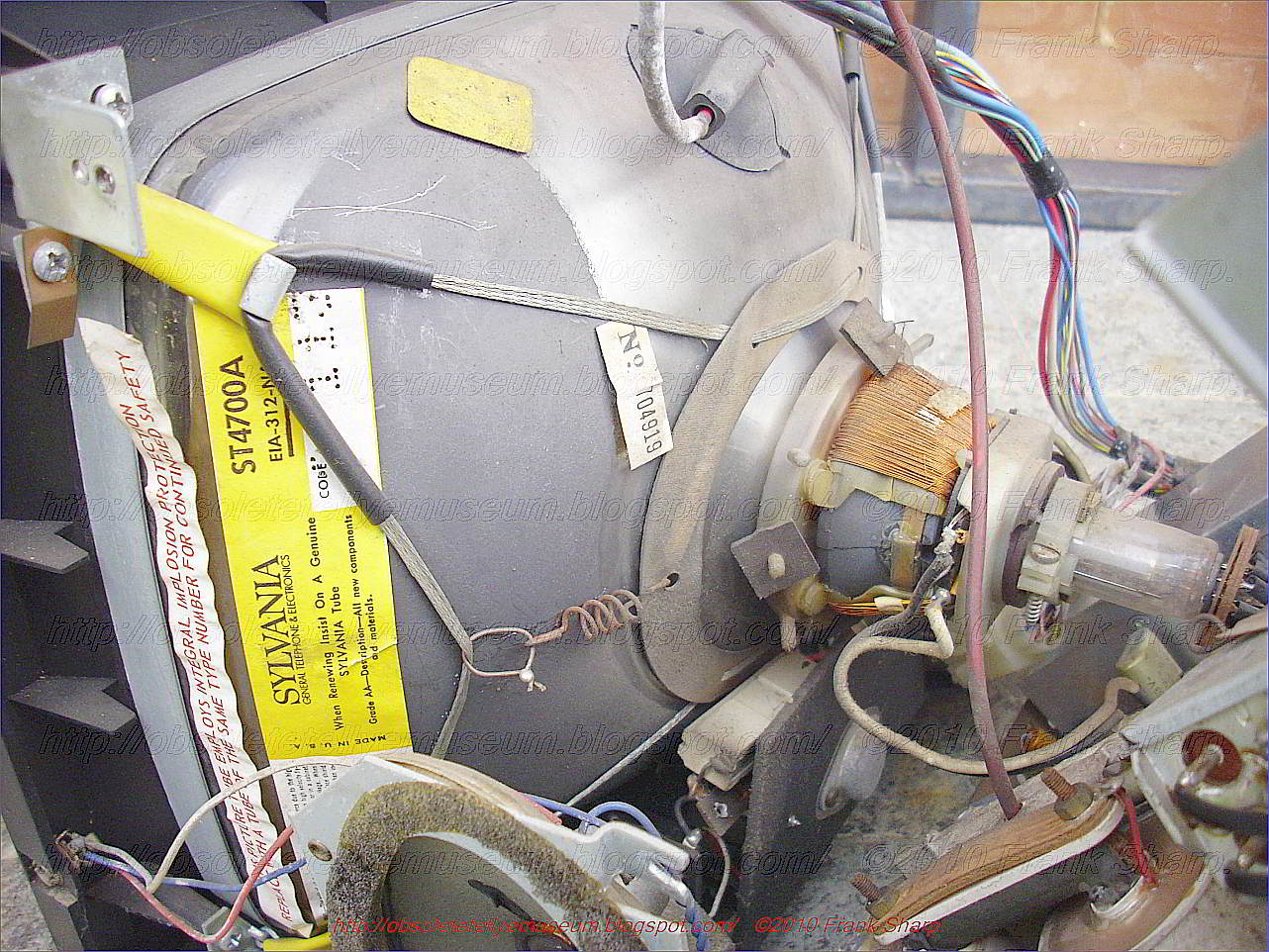
- The EHT Output is realized with a selenium rectifier.
The EHT selenium rectifier which is a Specially designed selenium rectifiers were once widely used as EHT rectifiers in television sets and photocopiers. A layer of selenium was applied to a sheet of soft iron foil, and thousands of tiny discs (typically 2mm diameter) were punched out of this and assembled as "stacks" inside ceramic tubes. Rectifiers capable of supplying tens of thousands of volts could be made this way. Their internal resistance was extremely high, but most EHT applications only required a few hundred microamps at most, so this was not normally an issue. With the development of inexpensive high voltage silicon rectifiers, this technology has fallen into disuse.
Power supply is realized with mains transformer and
Linear transistorized power supply stabilizer, A DC power supply
apparatus includes a rectifier circuit which rectifies an input
commercial AC voltage. The rectifier output voltage is smoothed in a
smoothing capacitor. Voltage stabilization is provided in the
stabilizing circuits by the use of Zener diode circuits to provide
biasing to control the collector-emitter paths of respective
transistors.A linear regulator circuit according to an embodiment of
the present invention has an input node receiving an unregulated
voltage and an output node providing a regulated voltage. The linear
regulator circuit includes a voltage regulator, a bias circuit, and a
current control device.In one embodiment, the current control device is implemented as an NPN bipolar junction transistor (BJT) having a collector electrode forming the input node of the linear regulator circuit, an emitter electrode coupled to the input of the voltage regulator, and a base electrode coupled to the second terminal of the bias circuit. A first capacitor may be coupled between the input and reference terminals of the voltage regulator and a second capacitor may be coupled between the output and reference terminals of the voltage regulator. The voltage regulator may be implemented as known to those skilled in the art, such as an LDO or non-LDO 3-terminal regulator or the like.
The bias circuit may include a bias device and a current source. The bias device has a first terminal coupled to the output terminal of the voltage regulator and a second terminal coupled to the control electrode of the current control device. The current source has an input coupled to the first current electrode of the current control device and an output coupled to the second terminal of the bias device. A capacitor may be coupled between the first and second terminals of the bias device.
In the bias device and current source embodiment, the bias device may be implemented as a Zener diode, one or more diodes coupled in series, at least one light emitting diode, or any other bias device which develops sufficient voltage while receiving current from the current source. The current source may be implemented with a PNP BJT having its collector electrode coupled to the second terminal of the bias device, at least one first resistor having a first end coupled to the emitter electrode of the PNP BJT and a second end, a Zener diode and a second resistor. The Zener diode has an anode coupled to the base electrode of the PNP BJT and a cathode coupled to the second end of the first resistor. The second resistor has a first end coupled to the anode of the Zener diode and a second end coupled to the reference terminal of the voltage regulator. A second Zener diode may be included having an anode coupled to the cathode of the first Zener diode and a cathode coupled to the first current electrode of the current control device.
A circuit is disclosed for improving operation of a linear regulator, having an input terminal, an output terminal, and a reference terminal. The circuit includes an input node, a transistor, a bias circuit, and first and second capacitors. The transistor has a first current electrode coupled to the input node, a second current electrode for coupling to the input terminal of the linear regulator, and a control electrode. The bias circuit has a first terminal for coupling to the output terminal of the linear regulator and a second terminal coupled to the control electrode of the transistor. The first capacitor is for coupling between the input and reference terminals of the linear regulator, and the second capacitor is for coupling between the output and reference terminals of the linear regulator. The bias circuit develops a voltage sufficient to drive the control terminal of the transistor and to operate the linear regulator. The bias circuit may be a battery, a bias device and a current source, a floating power supply, a charge pump, or any combination thereof. The transistor may be implemented as a BJT or FET or any other suitable current controlled device.
No comments:
Post a Comment
The most important thing to remember about the Comment Rules is this:
The determination of whether any comment is in compliance is at the sole discretion of this blog’s owner.
Comments on this blog may be blocked or deleted at any time.
Fair people are getting fair reply. Spam and useless crap and filthy comments / scrapers / observations goes all directly to My Private HELL without even appearing in public !!!
The fact that a comment is permitted in no way constitutes an endorsement of any view expressed, fact alleged, or link provided in that comment by the administrator of this site.
This means that there may be a delay between the submission and the eventual appearance of your comment.
Requiring blog comments to obey well-defined rules does not infringe on the free speech of commenters.
Resisting the tide of post-modernity may be difficult, but I will attempt it anyway.
Your choice.........Live or DIE.
That indeed is where your liberty lies.
Note: Only a member of this blog may post a comment.