


GRUNDIG XS70/1 CHASSIS CUC6360 (29701-088) :
CPU - XC68HC11F1B4
EEPROM - 24C04
EPROM - 27С1001
SMPS - TDA4605-3 + IRFBC40
IF - TDA6051-5
Tuner - 29504-201.21
Secam - TDA8395P
Delay - TDA4665
Video PROC- TDA8376
FRAME/Vertical - TDA8350Q
DSP - MSP3400
Sound AMP- TDA7262
TXT - SAA5281ZP/E
VIDEO Switch - TEA5114A
RGB Amp. - TEA5101A
LINE+EHT+FBT - M29201-029.52A
HOT - BU508A
IC remote - PCA84C122AT-094, MC144105, MC144107


 When the remote controller battery is exhausted to a low state, the
state is detected and displayed on a display device located at the
apparatus which is controlled by the commands from the remote
controller. The voltage state of the battery is detected upon the
actuation of a key of the remote controller. If a low state is detected,
a low battery data code is added to the command code generated as a
result of actuation of the key, and both kinds of data are transmitted
to the controlled electronic device. The transmitted data is received at
the controlled electronic device. The low battery data is detected and
displayed on a display device of the remotely controlled electronic
device.
When the remote controller battery is exhausted to a low state, the
state is detected and displayed on a display device located at the
apparatus which is controlled by the commands from the remote
controller. The voltage state of the battery is detected upon the
actuation of a key of the remote controller. If a low state is detected,
a low battery data code is added to the command code generated as a
result of actuation of the key, and both kinds of data are transmitted
to the controlled electronic device. The transmitted data is received at
the controlled electronic device. The low battery data is detected and
displayed on a display device of the remotely controlled electronic
device. 
mixing the battery exhaustion data with the inputted key data and transmitting them, upon determining that the battery of the remote controller is exhausted to b
elow a predetermined level; and receiving said remote controller data to decode it, and displaying after or before a key function through a display device of a set portion, upon finding a battery data in said received remote controller data.
2. The method for displaying the state of a remote controller battery as claimed in claim 1, wherein said transmitting step is performed with a data format decided by a protocol between a transmitting part and the receiving part.
3. The method for displaying the state of a remote controller battery as claimed in claim 1, wherein said remote controller data receiving step is composed to display a battery exhaustion state in the form of an on-screen display by character display by letters.
4. The method for displaying the state of a remote controller battery as claimed in claim 1, wherein said remote controller data receiving step is displayed through a light emitting diode which has been installed on said set portion.
5. The method for displaying the state of a remote controller battery as claimed in claim 1, wherein said remote controller data receiving step is displayed through a liquid crystal display installed on said set portion.
6. In a remote control system of the type including a remote controller powered by a battery and having keys which are depressed to result in command data codes being transmitted to a controlled electronic device, said electronic device carrying out the command designated by said command data codes, a method of displaying a low battery state of said battery, comprising the steps of:
providing low battery data representing the detection of said last mentioned condition;
transmitting said low battery data to said controlled electronic device;
detecting said low battery data at said controlled electronic device; and
displaying at said controlled electronic device, in response to a detection of said low battery data, an indication that said battery is at a voltage level below said predetermined level.
7. The method of claim 6, wherein the step of transmitting comprises transmitting said low battery data in combination with said command data codes.
8. The method of claim 7, wherein the step of detecting said battery condition comprises, sensing the actuation of any of said keys of said remote controller, and monitoring the voltage level of said battery each time actuation of a key is sensed.
9. The method of claim 6, wherein the step of detecting said battery condition comprises, sensing the actuation of any of said keys of said remote controller, and monitoring the voltage level of said battery each time actuation of a key is sensed.
10. In a remote control system of the type including a remote controller powered by a battery and having keys which are depressed to result in command data codes being transmitted to a controlled electronic device, said electronic device carrying out the command designated by said command data codes, apparatus for displaying a low battery state of said battery, comprising: detecting means at said remote controller for detecting the condition that said battery is providing power at a voltage level below a predetermined minimum level;
a microprocessor for providing low battery data representing the detection of said last mentioned condition; a transmitter for transmitting said low battery data to said controlled electronic device;
a receiver at said controlled electronic device for receiving data transmitted by said remote controller;
a detector at said controlled electronic device for detecting said low battery data in the data received by said receiver; and
a display device at said controlled electronic device for displaying, in response to a detection of said low battery data, an indication that said battery is at a voltage level below said predetermined level.
11. The apparatus of claim 10, wherein said microprocessor comprises means for adding said low battery data to said command data codes for combined transmission by said transmitter to said controlled electronic device.
12. The apparatus of claim 11, wherein said display device is a CRT.
13. The apparatus of claim 11, wherein said controlled electronic device is a television receiver and said display device is the video display screen of said television receiver.
14. The apparatus of claim 11, wherein said display device is an LED display device.
15. The apparatus of claim 11, wherein said display device is an LCD display device.
The present invention relates to a method for displaying the state of a battery in a remote control device, such that when the battery power is reduced
to
below a predetermined voltage level, this condition is detected and
displayed in the electronic apparatus, which is controlled by the remote
controller. Remote controllers are widely used on home appliances, and most of the remote controllers are equipped with batteries. If a remote controller is used for a long time, the power of the battery will become exhausted, such that the remote controller cannot function in the normal manner.
Because of such circumstances, conventionally a remote controller is provided with a liquid crystal display (LCD) or a light emitting diode (LED) to display the state of the battery. However, the user does not always watch the remote controller display and therefore will not always see the indication of reduced or exhausted battery power.
As a result of the state of the battery being displayed in a position often not noticed by the user, the user's first response to exhausted battery conditions is to assume that the electronic appliance is not working properly due to some malfunction, and the user will often contact a repair person to service the electronic appliance. Alternatively, the user may complain to the manufacturer of the electronic apparatus.
Another problem with the conventional remote control display of bat
tery power is that
the remote controller has to include a display, which increases the
manufacturing cost of the device. Japanese Patent Application Laid-Open No. Heisei-5-168068 (laid open on Jul. 2, 1993), entitled "Electronic Apparatus Provided with a Power Source State Checking Function", discloses an electronic apparatus, in which all the functions are controlled by a remote controller, and the state of a portable power source of the apparatus can be displayed on the remote controller, if the remote controller requests so. The main body of the apparatus, i.e. the controlled electronic apparatus, and the remote controller are capable of mutual transmission and reception of signals. If there is a request for a battery check from the remote controller to the main body, the main body detects the state of its battery and transmits a signal to the remote controller to indicate to the remote controller the state of the main body battery. The remote controller displays the received battery state data on the remote controller itself. However, this feature does not solve the above problem of the display and recognition of the battery power of the remote controller, itself.
SUMMARY OF THE INVENTION
The present invention is inten
ded to overcome the above-described disadvantages of the prior art. Therefore, it is an object of the present invention to provide a method and apparatus for displaying the state of a remote controller battery, in which, the low voltage state of the remote controller battery is detected, the detected state is transmitted to the electronic apparatus as an encoded signal, and the apparatus decodes the data and displays the received data on a display device of the apparatus, so that the user should be able to determine when the battery needs to be replaced.
In achieving the above object, the apparatus and method for displaying the remote controller battery according to the present invention carries out the steps of detecting the state of the battery in response to depressing a particular key on the remote control key board, transmitting to the electronic apparatus controlled by the remote controller a signal indicating the condition of the battery when the condition is a low battery state, and decoding the received signal in the apparatus, and displaying the information about the remote controller battery on a display of the apparatus.
a switch responsive to a first control signal having a controllable duty cycle and coupled to said source of input supply voltage for generating an output supply voltage, in accordance with said duty cycle of said first control signal;
a limiter coupled to said modulator for limiting the decrease in duty cycle, for a given increase in said input supply voltage, when said input supply voltage exceeds a first magnitude.
2. A power supply according to claim 1, wherein said duty cycle of said first control signal varies within a control range, in accordance with said second control signal, and wherein said limiter limits a decrease of said duty cycle when said duty cycle is at an end of said control range.
3. A power supply according to claim 1, wherein said limiter comprises a clamper coupled in a signal path of said input supply voltage indicative signal for clamping said input voltage indicative signal, when said input supply voltage exceeds said first magnitude, and for disabling the clamping thereof, when said input supply voltage does not exceed said first magnitude.
4. A power supply according to claim 3, wherein said voltage clamper comprises a diode.
5. A power supply according to claim 3, further comprising a disabling circuit responsive to said input supply voltage indicative signal for disabling said output supply voltage, when said input supply voltage is smaller than a second magnitude and wherein said voltage clamper is coupled in a common signal path of said input supply voltage indicative signal with respect to each of an input of said disabling circuit and an input of said limiter.
6. A power supply according to claim 1, wherein said modulator comprises a foldback point corrector for decreasing said duty cycle, when said input supply voltage increases and wherein said limiter is coupled to said corrector.
7. A power supply according to claim 1, wherein said second control signal is produced in a feedback path for regulating said output supply voltage.
8. A power supply according to claim 1, wherein said input supply voltage indicative signal is coupled to said modulator from said source of input supply voltage via a signal path that bypasses said switch.
9. A power supply according to claim 8, wherein said limiter comprises a clamp coupled in said signal path for clamping said input supply voltage indicative signal, when said input supply voltage exceeds said first magnitude, and for disabling the clamping operation, when said input supply voltage does not exceed said first magnitude.
10. A power supply, comprising: an input supply voltage, a transformer and a switch coupled for switch mode generation of a regulated output supply voltage,
said switch being responsive to a
first control signal having a controllable duty cycle; a duty cycle modulator for generating said first control signal responsive to a second control signal for limiting a duty cycle of said switch, said modulator operating in a first mode when said second control signal is in a predetermined range of voltage levels and operating in a second mode when said second control signal is outside of said range; and
a voltage monitor circuit for generating said second control signal, said second control signal representing a first proportion of said input supply voltage in a first range of input supply voltage values and a second proportion of said input supply voltage in a second range of input supply voltage values.
11. A power supply according to claim 10 wherein said voltage monitor circuit comprises a clamp coupled in a signal path of said second control signal.
12. A power supply according to claim 11, wherein said second signal is coupled to said modulator from said input supply voltage via a signal path that bypasses said switch.
13. A power supply, comprising: an input supply voltage, a tran
 sformer and a switch coupled for switch mode generation
of a regulated output supply voltage, said switch being responsive to a
first control signal having a controllable duty cycle;
sformer and a switch coupled for switch mode generation
of a regulated output supply voltage, said switch being responsive to a
first control signal having a controllable duty cycle; a duty cycle modulator for generating said first control signal responsive to a second control signal, said modulator operating in a first mode when said second control signal is in a predetermined range of voltage levels and operating in a second mode when said second control signal is outside of said range; and
a voltage monitor circuit for generating said second control signal, said second control signal representing a first proportion of said input supply voltage in a first range of input supply voltage values and a second proportion of said input supply voltage in a second range of input supply voltage values, such that as long as said input supply voltage is in said first range of input supply voltage values, said second control signal varies when said input supply voltage varies and said modulator operates in said first mode of operation.
14. A power supply, comprising: an input supply voltage, a transformer and a switch coupled for switch mode generation of a regulated output supply voltage, said switch being responsive to a first control signal having a controllable duty cycle;
a duty cycle modulator for generating said first control signal responsive to a second control signal, said modulator operating in a first mode when said second control signal is in a predetermined range of voltage levels and operating in a second mode when said second control signal is outside of said range; and
a nonlinear voltage divider circuit coupled to said input supply voltage for generating said second control signal, said second control signal representing a first proportion of said input supply voltage in a first range of input supply voltage values and a second proportion of said input supply voltage in a second range of input supply voltage values.
Switched-mode power supplies
efficiently generate a variety of regulated voltages
from a single line voltage level (e.g., 220 volts AC). One important use
of these power supplies is within a television signal receiver where
they are used to produce a regulated B+ voltage for the horizontal
deflection circuit as well as other regulated voltages for powering
various digital and analog circuits. Typically, a switched-mode power supply contains a full-wave rectifier, a power supply controller, a switch, and an output transformer. The switch is typically a high-power transistor such as a MOSFET. To regulate the output voltages, the controller activates and deactivates (e.g., pulse width modulates) the gate of the transistor in response to power supply loading and other control parameters. The switched voltage from the transistor drives a primary winding of the transformer, while various power supply loads are connected to one or more secondary windings. As such, the power supply converts an AC input voltage into one or more DC voltages.
One particular controller is an integrated circuit available from Siemens as Model TDA 4605. This power supply controller is typically used to drive the MOSFET transistor, which in turn drives the primary coil of the transformer. This specific integrated circuit, as well as others used in the art, typically contain a control mechanism that disables the power supply when the input voltage drops below a pre-defined voltage level. Such protection is necessary because, to produce regulated output voltages, the switched-mode power supply increases the duty cycle of the control signal driving the transistor as the input voltage decreases. At some point, the input voltage decreases to a level where the output of the power supply is unregulated (e.g., the maximum pulse length is used to drive the transistor). Such unregulated operation can damage the power supply electronics, but is more likely to damage the load electronics.
For the integrated circuit (IC) TDA4605, as defined in the TDA4605 Technical Manual available from Siemens AG, dated Jul. 27, 1989, pin 3 of the integrated circuit is used for sensing or monitoring the primary input voltage (vp) for the power supply (e.g., the rectified AC voltage). The threshold voltage for disabling or deactivating the integrated circuit, and thus the power supply, is pre-established by the controller at one volt. As such, the primary input voltage (vp) is reduced using a voltage divider at the input of pin 3. By selecting appropriate resistor
values within the voltage
divider, a nominal value of monitoring voltage is applied to pin 3.
Typically, this voltage is approximately 2.0 volts for a primary input
voltage of 120 volts. When the primary input voltage falls to a level
that causes the monitoring voltage at pin 3 to fall below one volt, the
power supply is deactivated to avoid unregulated operation. As stated above, this form of switched-mode power supply has been finding use within television signal receivers. However, television receivers, in particular, present peculiar loading characteristics to a power supply. Specifically, a television receiver power supply is called upon to produce a regulated B+ voltage, typically of approximately 140 volts, as well as a low voltage DC level of 16 volts for powering all of the digital and analog circuitry within the receiver. When the television receiver is switched from stand-by to run mode, a heavy load is produced by the in-rush of current into filter capacitors connected to the regulated B+ voltage. This heavy load causes the power supply to temporarily operate in an unregulated (maximum pulse width) mode, and may cause the primary input voltage to drop to a low level. Furthermore, when the degaussing circuit is activated to degauss the cathode ray tube (CRT), the main AC supply voltage is depressed due to the substantial load presented by the degaussing circuit. Consequently, the drop in line voltage could typically cause the monitoring voltage to drop below the 1 volt, first threshold level, and as such, to disable the power supply.
Therefore, there it is desirable to produce a monitoring voltage indicative of the primary input voltage, but to insure that the power supply will not be deactivated for the expected heavy loads found in a television receiver.
The IC TDA 4605 includes a foldback point correction circuit that reduces the maximum duty cycle of the MOSFET control signal, when the monitoring voltage exceeds a second threshold level of approximately 1.7 V. The monitoring voltage is applied to the correction circuit also via pin 3.
In a circuit embodying an inventive feature, a resistive voltage divider that produces the monitoring input or sense signal from the primary input voltage is designed such that the first threshold level is not attained during the expected temporary loading of the primary input voltage. However, such a voltage divider results in a higher voltage being applied to the monitoring voltage input of the controller during normal operation of the power supply. As such, an increase of the primary input voltage to a higher level, which is still within the acceptable tolerance range of the AC line voltage, can cause the monitoring voltage to rise to a level that exceeds the second
threshold
level at which the integrated circuit begins to limit the maximum duty
cycle of the control signal that controls the MOSFET, i.e., the
controller applies a foldback correction technique. When the second
threshold level is exceeded, the power supply automatically limits the
output power of the power supply for an increase in the primary voltage.
As a result of the voltage divider design that provides sufficient
headroom to overcome loading generated drop outs in the primary input
voltage, the maximum power supply output could be, undesirably,
significantly reduced at high primary input voltage. In carrying out an inventive feature, to insure that such inconsequential increase in the primary input voltage does not cause the power supply to significantly reduce the maximum duty cycle of the control signal and thereby, the power output of the power supply, a zener diode is coupled to the voltage divider. The zener diode limits the magnitude of the monitoring voltage to a level that avoids further maximum duty cycle limiting when the primary input voltage further increases. Consequently, when the power supply is used in a television signal receiver, the voltage divider provides enough head room for the primary voltage to drop substantially due to degaussing circuit activation or other loading conditions, while the zener diode insures that the primary voltage can rise above its nominal voltage without causing a significant power limitation of the power supply output.
A switch mode power supply, embodying an aspect of the invention, includes a source of an input supply voltage. A switch is responsive to a first control signal having a controllable duty cycle and coupled to the source of input supply voltage for generating an output supply voltage, in accordance with the duty cycle of the first control signal. A duty cycle modulator is responsive to a second control signal for generating the first control signal and for controlling the duty cycle of the first control signal in accordance therewith in a manner to control the current pulses. An increase in the duty cycle produces an increase in a magnitude of the current pulses. The modulator is responsive to a signal that is indicative of the input supply voltage for decreasing the duty cycle when the input supply voltage increases. A limiter is coupled to the modulator for limiting the decrease in duty cycle, for a given increase in said input supply voltage, when the input supply voltage exceeds a first magnitude.
FIG. 1 depicts a schematic diagram of a switched-mode power supply incorporating the teachings of the present invention.
FIG.
1 depicts a schematic diagram of a switched-mode power supply 100
incorporating the present invention. The embodiment shown is designed
for use as a power supply for a television signal receiver, wherein the
power supply generates a regulated B+ voltage (e.g., 140 volts) and a
low voltage (e.g., 16 volts). The regulated B+ voltage is used to power a
horizontal deflection circuit and the regulated low voltage is used to
power the digital and analog electronics (continuous load 118). Other
applications for the power supply may require slight variation in the
depicted components and their interconnections; however, such variations
are well within the scope of the present invention. The power supply contains a number of major components, including a full-wave rectifier 102, the power supply controller 106, a MOSFET transistor Q1, a monitor voltage generator 110, an output transformer 112, and a plurality of circuit components used to complete the power supply electronics. Illustratively, the input to the power supply is a 110-volt AC, 60 hertz voltage.
Rectifier 102 is a conventional full-wave bridge rectifier coupled to an AC input voltage source 101. The output of the bridge rectifier 102 is coupled to capacitor C1 approximately 680 μF). A voltage RAW B+ forms raw (unregulated) B+ voltage (also referred to herein as the primary input voltage vp) having a nominal value of approximately 150 volts. Capacitor C1, connected from the output of the rectifier to ground, smoothes the voltage from the bridge rectifier such that a DC voltage, i.e., the primary input voltage vp, is available at the upper terminal of the transformer's primary winding W1.
The primary input voltage forms an input to the monitor voltage generator 110 which produces a monitor voltage VZ1 for
the controller 106. The
monitor voltage generator is discussed in detail below. The controller is illustratively a TDA4605 power supply controller available from Siemens AG of Munich, Germany. The eight pins of the controller are connected to signals and voltages that enable the controller to produce a pulse width or duty cycle modulated signal at pin five for controlling the duty cycle of the transistor Q1. Specifically, pin 4 of controller 106 is grounded. Pin 3 is coupled to the monitor voltage.
Pin 2 is supplied information concerning the primary current. A primary current increase in the primary winding W1 is simulated as a voltage rise of a periodical, ramp voltage VC2 at pin 2 using an external RC element formed by resistor R3, capacitor C2, and resistor R4 (where R3 is approximately 360 kΩ, C2 is approximately 6,800 pF; and R4 is approximately 220 Ω). These elements are connected in series from the primary input voltage to ground. Pin 2 of the controller 106 is coupled to the junction of R3 and C2. A pulse width modulator 106c of the controller 106 controls the duration of the forward phase, and thus, the primary peak current, using ramp voltage VC2 that is proportional to the drain current of the transistor Q1. As indicated before, the ramp voltage is derived from the primary input voltage using the RC elements connected to pin 2, i.e., the ramp voltage simulates the primary current. Controller pin 1 is supplied secondary voltage information which internally compares the control voltage sampled from the regulating winding W3 of the transformer 112 and compares that sample voltage with an internal reference voltage.
Pin 5 generates a duty cycle modulated control signal or voltage VOUT via a push-pull output driver for rapid charge and discharge of the input capacitance of a MOSFET power transistor Q1 (Model IRF740).
Pin 6 is coupled to the supply voltage for the controller. Pin 7 forms a soft start input terminal. Capacitor C5 (0.1 μF) is connected from pin 7 to ground to reduce the pulse duration during start-up. Lastly, pin 8 is the input pin for the oscillator feedback.
In operation, the transistor Q1 is used as a power switch controlled by the controller 106. A snubber circuit is connected to the drain of the transistor Q1. The snubber circuit contains a combination of diode D3, resistor R16 and capacitor C12, which together limit the voltage overshoot when the transistor is turned off. D3 is a MUR450 diode, C12 is a 1000 pF capacitor, and R16 is a 2-watt, 30 kΩ resistor.
Together with the stray capacitance of the transformer, capacitor C7 (470 pF connected from drain terminal to ground) determines the no-load frequency, and consequently, the maximum slew rate of the drain voltage for a transistor Q1.
Transistor Q1 is driven with pulse width modulated signal VOUT produced at pin 5 of controller 106 and coupled to the gate terminal of the transistor via resistor R11 (35 Ω). Furthermore, a capacitor C6 (4700 pF) is coupled from the source terminal to the drain terminal. The source terminal is coupled to ground through resistor R13 (0.27 KΩ). Resistor R12 (10 kΩ) is optionally connected between the source terminal and gate terminal to ensure that the transistor will not be activated if power is applied to the power supply without the controller 106 being installed. The drain terminal is coupled to one terminal of the primary winding W1 of transformer 112. Consequently, the transistor Q1 controls the current flow from the primary input voltage thr
ough the primary winding. The secondary circuit of the transformer 112 consists of several windings, each of which has a different number of turns, polarity, and load capacity. Specifically, winding W2 forms the output voltage for the regulated B+, while winding W4 forms the output winding for the regulated 16-volt low voltage output, and winding W3 generates the feedback voltage for the controller 106.
The load circuitry includes, connected to winding W2, an output diode D4 and capacitor C13 that couple power to the horizontal deflection circuit 116. Additionally, the center tap of the output secondary winding is connected to ground, and winding W4 is coupled to diode D5 and capacitor C14. This output is the 16 volts that powers the continuous load 118 of the television receiver, e.g., all of the electronics and integrated circuits. This circuit 118 also controls the timing of when the degaussing circuit 114 is activated using degaussing control line 120. The control line for the continuous load is the run/standby control signal that essentially turns the television receiver on and off. The continuous load circuitry 118 is also coupled to the horizontal deflection circuit 116 to provide control signals therefor.
The controller 106 is started up using resistor R17 (100 KΩ) as a start resistor. As such, capacitor C11 (100 μF) is charged with half-wave currents at the voltage supply pin of the controller 106, e.g., pin 6. These half-wave currents are supplied from the primary input voltage through resistor R17 (100 KΩ) to ground through series connected resistor R14 (202 Ω), diode D
2 (148 Ω) and regulating winding
W3. When the voltage at C11 reaches the switch-on threshold, the
switched-mode power supply begins to function and supplies the feedback
voltage, via winding W3, resistor R14 and diode D2. This feedback
voltage, when rectified by diode D2 and smoothed by capacitor C11, forms
the supply voltage (vcc) for the controller 106 via pin 6. A control signal or voltage VCT for pin 1 is generated in a circuit parallel to the controller supply voltage circuit. The control voltage is produced by diode D1 (ERB43) charging capacitor C3 (1.5 μF) through resistor R8 (10 Ω). The RC element, consisting of series connected R15 (30 Ω) and C10 (0.01 μF), prevents peak value rectification of high frequency components of the feedback signal.
More specifically, regulating winding W3 is coupled to one terminal of resistor R15. The other terminal of resistor R15 is coupled to capacitor C10 to ground. Diode D1 is connected at the junction of resistor R15 and capacitor C10. Capacitor C9 (1000 pF) is connected in parallel with diode D1. Diode D1 has an output voltage that is coupled to series connected R8 and C3 which couples the output of the diode to ground. The output of the diode is also coupled through resistive divider network R6 and R7 which are respectively connected in series to ground. The voltage at the junction of R6 and R7 forms control voltage VCT and is coupled to pin 1 of the controller 106. These resistors define the no-load frequency of oscillation of the controller 106. Therefore, they are typically 0.1% accurate resistors having R6 being 5.49 KΩ, and R7 being 174 Ω. Control voltage VCT is coupled to a pulse-width modulator 106c within controller 106 that co
ntrols the duty cycle modulation of voltage VOUT for
regulating, for example, voltage REGB+. During the power supply start-up, capacitor C5 at the soft-start pin (e.g., pin 7), influences the duration of the forward phase by controlling the error voltage of the pulse width modulator. The controller detects the end of the transformer discharge phase via resistor R10 (20 KΩ) that is coupled at one end to controller pin 8 and at the other end to resistor R14, and ultimately to the regulating winding W3. Additionally, capacitor C8 (0.022 μF) is coupled from the junction of R10 and R14 to ground. At this point, the voltage changes polarity from positive to negative, i.e., the voltage represents zero crossings.
A voltage VZ1, embodying an inventive feature, is generated by the monitor voltage generator 110 and is coupled to pin 3 of the controller 106. Voltage VZ1 is used both for determining the minimum line voltage that will allow the power supply to operate and for controlling a foldback point correction circuit 106b within the controller 106.
The monitor voltage generator 110 contains resistor R1 (270 kΩ) coupled in series with resistor R2 (5100 Ω) to form a resistive voltage divider network with respect to primary input voltage RAW B+. The junction of the two resistors is coupled to the pin 3 of controller 106. Furthermore, a zener diode Z1 (B2X55/C3VO), embodying an inventive feature, is connected in parallel with resistor R2 from the junction point to ground. Zener diode Z1 forms a limiter for limiting the maximum voltage across R2 to the breakdown voltage of the zener diode Z1. Consequently, the voltage at the output of the monitor voltage generator 110 tracks the primary input voltage RAW B+ up to the threshold point where the zener diode Z1 begins to conduct.
The controller 106 includes an under-voltage detector 106a that uses a fixed, internal voltage threshold that causes the controller to disable the power supply whenever the monitor voltage VZ1 drops below a first threshold voltage. For the TDA 4605 integrated circuit, this first threshold voltage is one volt. As such, the divider network of R1 and R2 defines a voltage at the output that under typical operation would not cause the controller to deactivate the power supply.
In one particular application, e.g., a television signal receiver, a degaussing circuit 114 for a television signal receiver is typically connected directly across the input AC power. Consequently, when the degaussing circuit is activated, it will typically cause a drop in the AC voltage that is applied to the input of the voltage rectifier 102. Consequently,
the primary input
voltage RAW B+ will drop significantly during the degaussing period.
Since this is a normal behavior of a conventional television receiver
circuit, it is desirable that the monitor voltage generator 110 be
designed such that the controller 106 will not deactivate the power
supply during the degaussing period. For a primary input voltage of 120 volts and using a resistive divider of 270 KΩ for R1 and 5100 Ω for R2, the nominal voltage VZ1 at the voltage monitor input pin is 2 volts. Such a value for the voltage monitor voltage will avoid power supply deactivation during the degaussing period or other heavy load period.
When the duty cycle of voltage VOUT is at the maximum as a result of an overload condition, an increase in voltage RAW B+, produced by an increase in the AC line voltage, causes the voltage across primary winding w1 to increase. As the primary input voltage RAW B+ rises, the available input power to the power supply increases which could damage the power supply when the power supply is overloaded. During a period of overloaded, unregulated output, the modulator 106c generates the voltage VOUT having a maximum duty cycle for driving transistor Q1. As a result, a primary current IP in winding W1 of transformer 112 has also a maximum duty cycle. Therefore, undesirably an increase in voltage RAW B+ can produce a large voltage across the transistor that could damage the transistor or other circuitry.
To maintain the power supply within a safe operation range, the controller 106 includes what is known as a foldback or overload point correction circuit 106b. This foldback point correction circuit reduces the maximum duty cycle of voltage VOUT when the primary input voltage exceeds a predetermined magnitude. An increase above the predetermined magnitude causes the foldback point correction circuit 106b to decrease the maximum duty cycle of signal VOUT as voltage RAW B+ increases. The decrease is done by generating a correction curren
t ICOR
that is coupled to capacitor C2 causing an increase in the rate of
change of voltage VC2 at pin 2 of controller 106 when voltage VZ1
exceeds a second threshold voltage. When voltage RAW B+ increases and causes voltage VZ1 to further increase above the second threshold voltage an increase in current ICOR produces a decrease in the maximum duty cycle of signal VOUT, in a well know manner. The second threshold voltage occurs when voltage VZ1 is above a voltage level of approximately 1.7 V. The result is that, when voltage RAW B+ further increases the maximum duty cycle decreases proportionally. The decrease in the maximum duty cycle tends to stabilize the maximum power produced in the power supply against an increase of voltage RAW B+. On the other hand, an increase of voltage VZ1 when voltage VZ1 is below the 1.7 V level, does not affect current ICOR and the duty cycle of voltage VOUT.
Because the divider network (R1 and R2) establishes a sufficiently large monitor voltage VZ1 that provides sufficient headroom for preventing power supply shutdown when the degaussing circuit is activated, primary input voltage RAW B+ may be at a level that causes voltage VZ1 to exceed the second threshold voltage of circuit 106b by an excessive amount even when volt
age RAW B+ is within the normal tolerance range.
Therefore, disadvantageously, the maximum duty cycle may further
decrease by a significant amount in a manner to lower the maximum power
that can be derived. Such significant reduction in power capability can
occur even though primary input voltage is not truly at such a high
level that could damage the power supply. In accordance with an inventive feature, to prevent current ICOR from further reducing the maximum duty cycle of voltage VOUT when voltage RAW B+ increases above a threshold magnitude that corresponds to voltage VZ1 being equal to 3 V, the monitor voltage generator 110 contains the zener diode Z1 operating as a limiter which limits the primary input voltage indicative voltage VZ1 to 3 V. Consequently, the monitor voltage VZ1 can never rise above a pre-defined level (e.g., 3 volts) that would otherwise cause the foldback point correction circuit 106b within the controller 106 to further decrease the maximum duty cycle. In this way, advantageously, the decrease in the maximum duty cycle as a function of an increase in voltage RAW B+ is limited.
The decrease in the duty cycle of voltage VOUT produced by current ICOR, for a given increase in voltage RAW B+, is limited when voltage RAW B+ is greater than a threshold magnitude that corresponds to voltage VZ1 equal to 3 V. In contrast, the decrease in the duty cycle produced by current ICOR is not limited but varies proportionally to voltage RAW B+ when voltage VZ1 is between 1.7 V and 3 V. Thus, zener diode Z1 operates as a limiter for limiting the decrease in the duty cycle when the voltage RAW B+ exceeds the threshold magnitude relative to when voltage RAW B+ does not exceed the threshold magnitude. An increase in voltage RAW B+ that produces voltage VZ1 below the second threshold voltage of 1.7 V, does not affect current ICOR.
Specifically, for the TDA 4605 integrated circuit control, the zener diode has a value of three volts. Consequently, the input signal to the monitor voltage generator cannot rise above the three volt level before the zener diode will begin to conduct current to ground. As such, the monitor voltage generator establishes a range of voltages that pre-defines a range of primary input voltages at which the controller 106 operates in a normal manner that avoids both an undervoltage power supply deactivation and a further decrease in the maximum duty cycle. The input voltage dynamic range is thereby extended.
SIEMENS TDA4605-3 Control IC for Switched-Mode Power Supplies usingMOS-Transistor
The IC TDA4605-3 controls the MOS-power transistor and performs all necessary control and
protection functions in free running flyback converters. Because of the fact that a wide load range
is achieved, this IC is applicable for consumer as well as industrial power supplies.
The serial circuit and primary winding of the flyback transformer are connected in series to the input
voltage. During the switch-on period of the transistor, energy is stored in the transformer. During the
switch-off period the energy is fed to the load via the secondary winding. By varying switch-on time
of the power transistor, the IC controls each portion of energy transferred to the secondary side
such that the output voltage remains nearly independent of load variations. The required control
information is taken from the input voltage during the switch-on period and from a regulation winding
during the switch-off period. A new cycle will start if the transformer has transferred the stored
energy completely into the load.
In the different load ranges the switched-mode power supply (SMPS) behaves as follows:
No load operation
The power supply is operating in the burst mode at typical 20 to 40 kHz. The output voltage can be
a little bit higher or lower than the nominal value depending of the design of the transformer and the
resistors of the control voltage divider.
Nominal operation
The switching frequency is reduced with increasing load and decreasing AC-voltage.
The output voltage is only dependent on the load.
Overload point
Maximal output power is available at this point of the output characteristic.
Overload
The energy transferred per operation cycle is limited at the top. Therefore the output voltages
declines by secondary overloading.
Circuit DescriptionApplication Circuit
The application circuit shows a flyback converter for video recorders with an output power rating of
70 W. The circuit is designed as a wide-range power supply for AC-line voltages of 180 to 264 V.
The AC-input voltage is rectified by the bridge rectifier GR1 and smoothed by C1 . The NTC limits
the rush-in current.
In the period before the switch-on threshold is reached the IC is suppled via resistor R 1 ; during the
start-up phase it uses the energy stored in C2 , under steady state conditions the IC receives its
supply voltage from transformer winding n1 via diode D1. The switching transistor T1 is a BUZ 90.
The parallel connected capacitor C3 and the inductance of primary winding n 2 determine the
system resonance frequency. The R 2-C4-D2 circuitry limits overshoot peaks, and R 3 protects the
gate of T1 against static charges.
During the conductive phase of the power transistor T1 the current rise in the primary winding
depends on the winding inductance and the mains voltage. The network consisting of R 4-C5 is used
to create a model of the sawtooth shaped rise of the collector current. The resulting control voltage
is fed into pin 2 of the IC. The RC-time constant given by R 4-C5 must be designed that way that
driving the transistor core into saturation is avoided.
The ratio of the voltage divider R 10/R 11 is fixing a voltage level threshold. Below this threshold the
switching power supply shall stop operation because of the low mains voltage. The control voltage
present at pin 3 also determines the correction current for the fold-back point. This current added to
the current flowing through R 4 and represents an additional charge to C5 in order to reduce the turnon
phase of T1. This is done to stabilize the fold-back point even under higher mains voltages.
Regulation of the switched-mode power supplies via pin 1. The control voltage of winding n1 during
the off period of T1 is rectified by D3, smoothed by C6 and stepped down at an adjustable ratio by
R 5 , R 6 and R 7 . The R 8-C7 network suppresses parasitic overshoots (transformer oscillation). The
peak voltage at pin 2, and thus the primary peak current, is adjusted by the IC so that the voltage
applied across the control winding, and hence the output voltages, are at the desired level.
When the transformer has supplied its energy to the load, the control voltage passes through zero.
The IC detects the zero crossing via series resistors R 9 connected to pin 8. But zero crossings are
also produced by transformer oscillation after T1 has turned off if output is short-circuited. Therefore
the IC ignores zero crossings occurring within a specified period of time after T1 turn-off.
The capacitor C8 connected to pin 7 causes the power supply to be started with shorter pulses to
keep the operating frequency outside the audible range during start-up.
On the secondary side, five output voltages are produced across winding n3 to n7 rectified by D4 to
D8 and smoothed by C9 to C13 . Resistors R 12 , R 14 and R 19 to R 21 are used as bleeder resistors.
Fusable resistors R 15 to R 18 protect the rectifiers against short circuits in the output circuits, which
are designed to supply only small loads.
Pin 1
The regulating voltage forwarded to this pin is compared with a stable internal reference voltage VR
in the regulating and overload amplifier. The output of this stage is fed to the stop comparator. Ifthe control voltage is rather small at pin 1 an additional current is added by means of current source
which is controlled according the level at pin 7. This additional current is virtually reducing the
control voltage present at pin 1.
Pin 2
A voltage proportional to the drain current of the switching transistor is generated there by the
external RC-combination in conjunction with the primary current transducer. The output of this
transducer is controlled by the logic and referenced to the internal stable voltage V2B . If the voltage
V2 exceeds the output voltage of the regulations amplifier, the logic is reset by the stop comparator
and consequently the output of pin 5 is switched to low potential. Further inputs for the logic stage
are the output for the start impulse generator with the stable reference potential VST and the
supply voltage motor.
Pin 3
The down divided primary voltage applied there stabilizes the overload point. In addition the logic is
disabled in the event of low voltage by comparison with the internal stable voltage VV in the primary
voltage monitor block.
Pin 4
Ground
Pin 5
In the output stage the output signals produced by the logic
are shifted to a level suitable for MOSpowertransistors.
Pin 6
From the supply voltage V6 are derived a stable internal references VREF and the switching
threshold V6A , V6E , V6 max and V6 min for the supply voltage monitor. All references values (VR ,
V2B , VST) are derived from VREF . If V6 > VVE , the VREF is switched on and switched off when V6 <
V 6A . In addition, the logic is released only for V6 min < V6 < V6 max .
Pin 7
The output of the overload amplifier is connected to pin 7. A load on this output causes a reduction
in maximal impulse duration. This function can be used to implement a soft start, when pin 7 is
connected to ground by a capacitor.
Pin 8
The zero detector controlling the logic block recognizes the transformer being discharged by
positive to negative zero crossing of pin 8 voltage and enables the logic for a new pulse. Parasitic
oscillations occurring at the end of a pulse cannot lead to a new pulse (double pulsing), because an
internal circuit inhibits the zero detector for a finite time tUL after the end of each pulse.
Start-Up Behaviour
The start-up behaviour of the application circuit per sheet 88 is represented an sheet 90 for a linevoltage barely above the lower acceptable limit time t0 the following voltages built up:
– V6 corresponding to the half-wave charge current over R1
– V2 to V2 max (typically 6.6 V)
– V3 to the value determined by the divider R 10/R 11 .
The current drawn by the IC in this case is less than 1.6 mA.
If V6 reaches the threshold V6E (time point t1), the IC switches on the internal reference voltage. The
current draw max. rises to 12 mA. The primary current- voltage reproducer regulates V2 down to V2B
and the starting impulse generator generates the starting impulses from time point t5 to t6 . The
feedback to pin 8 starts the next impulse and so on. All impulses including the starting impulse are
controlled in width by regulating voltage of pin 1. When switching on this corresponds to a shortcircuit
event, i.e. V1 = 0. Hence the IC starts up with "short-circuit impulses" to assume a width
depending on the regulating voltage feedback (the IC operates in the overload range). The IC
operates at the overload point. Thereafter the peak values of V2 decrease rapidly, as the starting
attempt is aborted (pin 5 is switched to low). As the IC remains switched on, V6 further decreases
to V6 . The IC switches off; V6 can rise again (time point t4) and a new start-up attempt begins at
time point t1 . If the rectified alternating Iine voltage (primary voltage) collapses during load, V3 can
fall below V3A , as is happening at time point t3 (switch-on attempt when voltage is too low). The
primary voltage monitor then clamps V3 to V3S until the IC switches off (V6 < V6A). Then a new startup
attempt begins at time point t1 .
Regulation, Overload and No-Load Behaviour
When the IC has started up, it is operating in the regulation range. The potential at pin 1 typically is400 mV. If the output is loaded, the regulation amplifier allows broader impulses (V5 = H). The peak
voltage value at pin 2 increases up to V2S max . If the secondary load is further increased, the
overload amplifier begins to regulate the pulse width downward. This point is referred to as the
overload point of the power supply. As the IC-supply voltage V6 is directly proportional to the
secondary voltage, it goes down in accordance with the overload regulation behaviour. If V6 falls
below the value V6 min , the IC goes into burst operation. As the time constant of the half-wave
charge-up is relatively large, the short-circuit power remains small. The overload amplifier cuts back
to the pulse width tpk . This pulse width must remain possible, in order to permit the IC to start-up
without problems from the virtual short-circuit, which every switching on with V1 = 0 represents. If
the secondary side is unloaded, the loading impulses (V5 = H) become shorter. The frequency
voltages and V6 increase. When V6 = V6 max the logic is blocked. The IC converts to burst
operation.This renders the circuit absolutely safe under no-load conditions.
Behaviour when Temperature Exceeds Limit
An integrated temperature protection disables the logic when the chip temperature becomes too
high. The IC automatically interrogates the temperature and starts as soon as the temperature
decreases to permissible values.
PHILIPS TDA8376 family I2C-bus controlled economy PAL/NTSC and NTSC TV-processors:
GENERAL DESCRIPTIONThe various versions of the TDA837x series are I2C-bus
controlled single-chip TV processors which are intended to
be applied in PAL/NTSC (TDA8374 and TDA8375) and
NTSC (TDA8373 and TDA8377) television receivers.
All ICs are available in an SDIP56 package and some
versions are also available in a QFP64 package. The ICs
are pin compatible so that with one application board
NTSC and PAL/NTSC (or multistandard together with the
SECAM decoder TDA8395) receivers can be built.
Functionally this IC series is split in to 2 categories:
• Versions intended to be used in economy TV receivers
with all basic functions
• Versions with additional functions such as E-W
geometry control, horizontal and vertical zoom function
and YUV interface which are intended for TV receivers
with 110° picture tubes.
FEATURES
Available in all ICs:
• Vision IF amplifier with high sensitivity and good figures
for differential phase and gain
• PLL demodulator for the IF signal
• Alignment-free sound demodulator
• Flexible source selection with a CVBS input for the
internal signal and Y/C or CVBS input for the external
signal
• Audio switch
• The output signal of the CVBS (Y/C) switch is externally
available
• Integrated chrominance trap and band-pass filters
(auto-calibrated)
• Luminance delay line integrated
• A symmetrical peaking circuit in the luminance channel
• Black stretching of non-standard CVBS or luminance
signals
• RGB control circuit with black current stabilization and
white point adjustment
• Linear RGB inputs and fast blanking
• Horizontal synchronization with two control loops and
alignment-free horizontal oscillator
• Slow start and slow stop of the horizontal drive pulses
• Vertical count-down circuit
• Vertical driver optimized for DC-coupled vertical output
stages
• I2C-bus control of various functions
• Low dissipation
• Small amount of peripheral components compared with
competition ICs.
FUNCTIONAL DESCRIPTIONVision IF amplifier
The IF amplifier contains 3 AC-coupled control stages with
a total gain control range which is higher than 66 dB.
The sensitivity of the circuit is comparable with that of
modern IF-ICs.
The video signal is demodulated by a PLL carrier
regenerator. This circuit contains a frequency detector and
a phase detector. During acquisition the frequency
detector will tune the VCO to the correct frequency.
The initial adjustment of the oscillator is realized via the
I2C-bus.
The switching, between SECAM L and L’, can also be
realized via the I2C-bus. After lock-in the phase detector
controls the VCO so that a stable phase relationship
between the VCO and the input signal is achieved.
The VCO operates at twice the IF frequency.
The reference signal for the demodulator is obtained by
using a frequency divider circuit.
The AFC output is obtained by using the VCO control
voltage of the PLL and can be read via the I2C-bus.
For fast search tuning systems the window of the AFC can
be increased by a factor of 3. The setting is realized with
the AFW bit.
Depending on the device type the AGC detector operates
on top-sync level (single standard versions) or on top-sync
and top-white level (multistandard versions).
The demodulation polarity is switched via the I2C-bus.
The AGC detector time constant capacitor is connected
externally. This is mainly because of the flexibility of the
application. The time constant of the AGC system during
positive modulation is rather long, this is to avoid visible
variations of the signal amplitude. To improve the speed of
the AGC system, a circuit has been included which detects
whether the AGC detector is activated every frame period.
When, during 3 frame periods, no action is detected the
speed of the system is increased. For signals without
peak-white information the system switches automatically
to a gated black level AGC. Because a black level clamp
pulse is required for this method of operation the circuit will
only switch to black level AGC in the internal mode.
The circuits contain a second fast video identification
circuit which is independent of the synchronization
identification circuit. Consequently, search tuning is also
possible when the display section of the receiver is used
as a monitor. However, this identification circuit cannot be
made as sensitive as the slower sync identification circuit
(SL) and it is recommended to use both identification
outputs to obtain a reliable search system.
The identification output is applied to the tuning system via
the I2C-bus.
The input of the identification circuit is connected to pin 13,
the internal CVBS input (see Fig.1). This has the
advantage that the identification circuit can also be made
operative when a scrambled signal is received
[descrambler connected between the IF video output
(pin 6) and pin 13]. A second advantage is that the
identification circuit can be used when the IF amplifier is
not used (e.g. with built-in satellite tuners).
The video identification circuit can also be used to identify
the selected CBVS or Y/C signal. The switching between
the two modes can be realized with bit VIM.
Video switches
The circuit has two CVBS inputs (CVBSint and CVBSext)
and a Y/C input. When the Y/C input is not required pin 11
can be used as the third CVBS input. The switch
configuration is illustrated i
n Fig.7. The selection of thevarious sources is made via the I2C-bus.
The output signal of the CVBS switch is externally
available and can be used to drive the teletext decoder, the
SECAM add-on decoder and a comb filter.
In applications with comb filters a Y/C input is only possible
when additional switches are added. In applications
without comb filters the Y/C input signal can be switched
to the CVBS output.
Sound circuitThe sound band-pass and trap filters have to be
connected externally. The filtered intercarrier signal is fed
to a limiter circuit and is demodulated by a PLL
demodulator. This PLL circuit automatically tunes to the
incoming carrier signal, hence no adjustment is required.
The volume is controlled via the I2C-bus. The de-emphasis
capacitor has to be connected externally.
The non-controlled audio signal can be obtained from this
pin (pin 55) (via a buffer stage).
The FM demodulator can be muted via the I2C-bus. This
function can be used to switch-off the sound during a
channel change so that high output peaks are prevented
(also on the de-emphasis output).
The TDA8373 and TDA8374 contain an Automatic Volume
Levelling (AVL) circuit which automatically stabilizes the
audio output signal to a certain level which can be set by
the user via the volume control. This function prevents big
audio output fluctuations due to variations of the
modulation depth of the transmitter. The AVL function can
be activated via the I2C-bus.
Synchronization circuit
The sync separator is preceded by a controlled amplifier
which adjusts the sync pulse amplitude to a fixed level.
These pulses are fed to the slicing stage which operates at
50% of the amplitude.
The separated sync pulses are fed to the first phase
detector and to the coincidence detector. The coincidence
detector is used to detect whether the line oscillator is
synchronized and can also be used for transmitter
identification. The circuit can be made less sensitive by
using the STM bit. This mode can be used during search
tuning to ensure that the tuning system will not stop at very
weak input signals. The first PLL has a very high static
steepness so that the phase of the picture is independent
of the line frequency.
The line oscillator operates at twice the line frequency.
The oscillator capacitor is internal. Because of the spread
of internal components an automatic calibration circuit has
been added to the IC. The circuit compares the oscillator
frequency with that of the crystal oscillator in the colour
decoder.
This results in a free-running frequency which deviatesless than 2% from the typical value. When the IC is
switched on the horizontal output signal is suppressed and
the oscillator is calibrated as soon as all subaddress bytes
have been sent. When the frequency of the oscillator is
correct the horizontal drive signal is switched on. To obtain
a smooth switching on and switching off behaviour of the
horizontal output stage the horizontal output frequency is
doubled during switch-on and switch-off (slow start/stop).
During that time the duty cycle of the output pulse has such
a value that maximum safety is obtained for the output
stage.
To protect the horizontal output transistor, the horizontal
drive is immediately switched off (via the slow stop
procedure) when a power-on rese
t is detected. The drivesignal is switched on again when the normal switch-on
procedure is followed, i.e. all subaddress bytes must be
sent and, after calibration, the horizontal drive signal will
be released again via the slow start procedure.
When the coincidence detector indicates an out-of-lock
situation the calibration procedure is repeated.
The circuit has a second control loop to generate the drive
pulses for the horizontal driver stage. The horizontal
output is gated with the flyback pulse so that the horizontal
output transistor cannot be switched on during the flyback
time.
Adjustments can be made to the horizontal shift, vertical
shift, vertical slope, vertical amplitude and the S-correction
via the I2C-bus. In the TDA8375A, TDA8377A, TDA8375
and TDA8377 the E-W drive can also be adjusted via the
I2C-bus. The TDA8375 and TDA8377 have a flexible zoom
adjustment possibility for the vertical and horizontal
deflection. When the horizontal scan is reduced to display
4 : 3 pictures on a 16 : 9 picture tube an accurate video
blanking can be switched on to obtain well defined edges
on the screen. The geometry processor has a differential
output for the vertical drive signal and a single-ended
output for the E-W drive (TDA8375A, TDA8377A,
TDA8375 and TDA8377). Overvoltage conditions (X-ray
protection) can be detected via the EHT tracking pin.
When an overvoltage condition is detected the horizontal
output drive signal will be switched off via the slow stop
procedure. However, it is also possible that the drive is not
switched off and that just a protection indication is given in
the I2C-bus output byte. The choice is made via the input
bit PRD. The ICs have a second protection input on the
phase-2 filter capacitor pin. When this input is activated the
drive signal is switched off immediately (without slow stop)
and switched on again via the slow start procedure.
For this reason this protection input can be used as ‘flash
protection’.
The drive pulses for the vertical sawtooth generator are
obtained from a vertical countdown circuit. This countdown
circuit has various windows depending on the incoming
signal (50 or 60 Hz and standard or non-standard).
The countdown circuit can be forced in various modes via
the I2C-bus. To obtain short switching times of the
countdown circuit during a channel change the divider can
be forced in the search window using the NCIN bit.
The vertical deflection can be set in the de-interlace mode
via the I2C-bus.
To avoid damage of the picture tube when the vertical
deflection fails, the guard output current of the TDA8350
and TDA8351 can be supplied to the beam current limiting
input. When a failure is detected the RGB outputs are
blanked and a bit is set (NDF) in the status byte of the
I2C-bus. When no vertical deflection output stage is
connected this guard circuit will also blank the output
signals. This can be overruled using the EVG bit.
Chrominance and luminance processing
The circuit contains a chrominance band-pass and trap
circuit. The filters are realized by using gyrator circuit
s.They are automatically calibrated by comparing the tuning
frequency with the crystal frequency of the decoder.
The luminance delay line and the delay for the peaking
circuit are also realized by using gyrator circuits.
The centre frequency of the chrominance band-pass filter
is 10% higher than the subcarrier frequency. This
compensates for the high frequency attenuation of the IF
saw filter. During SECAM reception the centre frequency
of the chrominance trap is reduced to obtain a better
suppression of the SECAM carrier frequencies. All ICs
have a black stretcher circuit which corrects the black level
for incoming video signals which have a deviation between
the black level and the blanking level (back porch).
The TDA8375A, TDA8377A, TDA8375 and TDA8377
have a defeatable coring function in the peaking circuit.
Some of the ICs have a YUV interface so that picture
improvement ICs such as the TDA9170 (contrast
improvement), TDA9177 (sharpness improvement) and
TDA4556 and TDA4566 (CTI) can be applied. When the
TDA4556 or TDA4566 is applied it is possible to increase
the gain of the luminance channel by using the GAI bit in
subaddress 03 so that the resulting RGB output signals
will not be affected.
Colour decoderDepending on the IC type the colour decoder can decode
NTSC signals (TDA8373 and TDA8377) or PAL/NTSC
signals (TDA8374 and TDA8375). The circuit contains an
alignment-free crystal oscillator, a killer circuit and two
colour difference demodulators. The 90° phase shift for the
reference signal is made internally.
The TDA8373 and TDA8377 contain an Automatic Colour
Limiting (ACL) circuit which prevents over saturation
occurring when signals with a high chroma-to-burst ratio
are received. This ACL function is also available in the
TDA8374 and TDA8375, however, it is only active during
the reception of NTSC signals.
The TDA8373 and TDA8377 have a switchable colour
difference matrix (via the I2C-bus) so that the colour
reproduction can be adapted to the market requirements.
In the TDA8374 and TDA8375 the colour difference matrix
switches automatically between PAL and NTSC, however,
it is also possible to fix the matrix in the PAL standard.
The TDA8374 and TDA8375 can operate in conjunction
with the SECAM decoder TDA8395 so that an automatic
multistandard decoder can be realized. The subcarrier
reference output for the SECAM decoder can also be used
as a reference signal for a comb filter. Consequently, the
reference sig
nal is continuously available when PAL orNTSC signals are detected and only present during the
vertical retrace period when a SECAM signal is detected.
Which standard the TDA8374 and TDA8375 can decode
depends on the external crystals. The crystal to be
connected to pin 34 must have a frequency of 3.5 MHz
(NTSC-M, PAL-M or PAL-N). Pin 35 can handle crystals
with a frequency of 4.4 and 3.5 MHz. Because the crystal
frequency is used to tune the line oscillator, the value of
the crystal frequency must be communicated to the IC via
the I2C-bus. It is also possible to use the IC in the so called
‘3-norma’ mode for South America. In that event one
crystal must be connected to pin 35 and the other two to
pin 34. Switching between the 2 latter crystals must be
performed externally. Consequently, the search loop of the
decoder must be controlled by the microcontroller.
To prevent calibration problems of the horizontal oscillator
the external switching between the two crystals should be
performed when the oscillator is forced to pin 35.
For a reliable calibration of the horizontal oscillator it is
very important that the crystal indication bits (XA and XB)
are not corrupted. For this reason the crystal bits can be
read in the output bytes so that the software can check the
I2C-bus transmission.
RGB output circuit and black current stabilization
The colour difference signals are matrixed with the
luminance signal to obtain the RGB signals. Linear
amplifiers have been chosen for the RGB inputs so that the
circuit is suited for signals that are input from the SCART
connector. The insertion blanking can be switched on or off
using the IE1 bit. To ascertain whether the insertion pin
has a (continuous) HIGH level or not can be read via the
IN1 bit. The contrast and brightness control operate on
internal and external signals.
The output signal has an amplitude of approximately 2 V
(black-to-white) at nominal input signals and nominal
settings of the controls. To increase the flexibility of the IC
it is possible to add OSD and/or teletext signals directly at
the RGB outputs. This insertion mode is controlled via the
insertion input. The action to switch the RGB outputs to
black has some delay which must be compensated for
externally.
The black current stabilization is realized by using a
feedback from the video output amplifiers to the RGB
control circuit. The black current of the 3 guns of the
picture tube is internally measured and stabilized.
The black level control is active during 4 lines at the end of
the vertical blanking. The vertical blanking is adapted to
the incoming CVBS signal (50 or 60 Hz). When the flyback
time of the vertical output stage is longer than the 60 H
zblanking time, or when additional lines need to be blanked
(e.g. for close captioning lines) the blanking can be
increased to the same value as that of the 50 Hz blanking.
This can be set using the LBM bit. The leakage current is
measured during the first line and, during the following
3 lines, the 3 guns are adjusted to the required level.
The maximum acceptable leakage current is ±100 µA.
The nominal value of the black current is 10 µA. The ratio
of the currents for the various guns automatically tracks
with the white point adjustment so that the background
colour is the same as the adjusted white point.
The input impedance of the black current measuring pin is14 kΩ. To prevent the voltage on this pin exceeding the
supply voltage during scan an internal protection diode
has been included.
When the TV receiver is switched on the black current
stabilization circuit is not active, the RGB outputs are
blanked and the beam current limiting input pin is
short-circuited. Only during the measuring lines will the
outputs supply a voltage of 4.2 V to the video output stage
to ascertain whether the picture tube is warming up. As
soon as the current supplied to the measuring input
exceeds a value of 190 µA the stabilization circuit will be
activated. After a waiting time of approximately 0.8 s the
blanking and beam current limiting input pins are released.
The remaining switch-on behaviour of the picture is
determined by the external time constant of the beam
current limiting network.
Adjustment of geometry control parameters
The deflection processor of the TDA8373 and TDA8374
offers 5 control parameters for picture alignment:
• Vertical picture alignment
– S-correction
– vertical amplitude
– vertical slope
– vertical shift
– Horizontal shift alignment.
The TDA8375, TDA8377, TDA8375A and TDA8377A offer
in addition the following functions for horizontal alignment:
• E-W width
• E-W parabola/width
• E-W corner/parabola
• E-W trapezium correction.
It is important to notice that the ICs are designed for use
with a DC-coupled vertical deflection stage. This is the
reason why a vertical linearity alignment is not necessary
(and, therefore, not available).
For a particular combination of picture tube type and
vertical output stage and E-W output stage, it is
determined which are the required values for the settings
of S-correction. These parameters can be preset via the
I2C-bus and do not need any additional a
djustment.The remainder of the parameters are preset with the
mid-value of their control range (i.e. 1FH), or with the
values obtained by previous TV set adjustments.
The vertical shift control is intended for compensation of
off-sets in the external vertical output stage or in the
picture tube. It can be shown that without compensation
these off-sets will result in a certain linearity error,
especially with picture tubes that need large S-correction.
The total linearity error is in 1st order approximation
proportional to the value of the off-set and to the square of
the S-correction needed. The necessity to use the vertical
shift alignment depends on the expected off-sets in vertical
output stage and picture tube, on the required value of the
S-correction and on the demands upon vertical linearity.
For adjustment of the vertical shift and vertical slope
independent of each other, a special service blanking
mode can be entered by setting the SBL bit HIGH. In this
mode the RGB outputs are blanked during the second half
of the picture. There are 2 different methods for alignment
of the picture in vertical direction. Both methods make use
of the service blanking mode.
The first method is recommended for picture tubes that
have a marking for the middle of the screen. With the
vertical shift control the last line of the visible picture is
positioned exactly in the middle of the screen. After this
adjustment the vertical shift should not be changed.
The top of the picture is placed by adjusting the vertical
amplitude and the bottom by adjusting the vertical slope.
The second method is recommended for picture tubes that
have no marking for the middle of the screen. For this
method a video signal is required in which the middle of the
picture is indicated (e.g. the white line in the circle test
pattern). With the vertical slope control the beginning of the
blanking is positioned exactly on the middle of the picture.
Then the top and bottom of the picture are placed
symmetrically with respect to the middle of the screen by
adjustment of the vertical amplitude and vertical shift. After
this adjustment the vertical shift has the correct setting and
should not be changed.
If the vertical shift alignment is not required VSH should be
set to its mid-value (i.e. VSH = 1FH). The top of the picture
is then placed by adjusting the vertical amplitude and the
bottom by adjusting the vertical slope. After the vertical
picture alignment the picture is positioned in the horizontal
direction by adjusting the horizontal shift.
To obtain the full range of the vertical zoom function with
the TDA8375 and TDA8377 the adjustment of the vertical
geometry should be carried out at a nominal setting of the
zoom DAC at position 19H.
PHILIPS TDA4665
Baseband delay line:GENERAL DESCRIPTION
The TDA4665 is an integrated baseband delay line circuit
with one line delay. It is suitable for decoders with
colour-difference signal outputs ±(R−Y) and ±(B−Y).
FEATURES
• Two comb filters, using the switched-capacitor
technique, for one line delay time (64 µs)
• Adjustment-free application
• No crosstalk between SECAM colour carriers (diaphoty)
• Handles negative or positive colour-difference input
signals
• Clamping of AC-coupled input signals (±(R−Y) and
±(B−Y))
• VCO without external components
• 3 MHz internal clock signal derived from a 6 MHz CCO,
line-locked by the sandcastle pulse (64 µs line)
• Sample-and-hold circuits and low-pass filters to
suppress the 3 MHz clock signal
• Addition of delayed and non-delayed output signals
• Output buffer amplifiers
• Comb filtering functions for NTSC colour-difference
signals to suppress cross-colour.
PHILIPS TDA4566 Colour transient improvement circuit:
The TDA4566 is a monolithic integrated circuit for colour-transient improvement (CTI) and luminance delay line in gyrator
technique in colour television receivers.
Features
• Colour transient improvement for colour difference signals (R-Y) and (B-Y) with transient detecting-, storage- and
switching stages resulting in high transients of colour difference output signals
• A luminance signal path (Y) which substitutes the conventional Y-delay coil with an integrated Y-delay line
• Switchable delay time from 550 ns to 820 ns in steps of 90 ns and additional fine adjustment of 37 ns
• Two Y output signals; one of 180 ns less delay
ITT / MICRONAS MSP340
0C Multistandard Sound Processor:1. Introduction
The MSP 3400C is designed as single-chip Multistan-
dard Sound Processor for applications in analog and
digital TV sets, satellite receivers and video recorders.
The MSP-family, which is based on the MSP 2400, dem-
onstrates the progressive development towards highly
integrated multi-functional ICs.
The MSP 3400C, again, improves function integration:
The full TV sound processing, starting with analog
sound IF signal-in, down to processed analog AF-out, is
performed in a single chip. The IC is produced in 0.8 µm
CMOS technology, combined with high performance
digital signal processing.
The MSP 3400C 0.8 µ CMOS version is fully pin and
software compatible to the 1.0 µ MSP 3400 and MSP
3410. The main difference between the MSP 3400C and
the MSP 3410, consists of the MSP 3410 being able to
decode NICAM signals.
2. Features of the MSP 3400C
2.1. Features of the Demodulator and Decoder
Sections
The MSP 3400C is designed to perform demodulation
of FM-mono
TV sound and two carrier FM systems ac-cording to the German or Korean terrestrial specs. With
certain constraints, it is also possible to do AM-demodu-
lation according to the SECAM system. Alternatively, the
satellite specs can be processed with the MSP 3400C.
For FM carrier detection in satellite operation, the AM-
demodulation offers a powerful feature to calculate the
carrier field strength, which can be used for automatic
search algorithms. So, the IC facilitates a first step to-
wards multistandard capability with its very flexible
application and may be used in TV-sets, satellite tuners,
and video recorders.
The MSP 3400C facilitates profitable multistandard ca-
pability, offering the following advantages:
– two selectable analog inputs (TV and SAT-IF sources)
– Automatic Gain Control (AGC) for analog input: input
range: 0.14 – 3 Vpp
– integrated A/D converter for sound-IF inputs
– all demodulation and filtering is performed on chip and
is individually programmable
– no external filter hardware is required
– only one crystal clock (18.432 MHz) is necessary
– FM carrier level calculation for automatic search algo-
rithms and carrier mute function
– high deviation FM-mono mode (max. deviation:
approx. ?360 kHz)
2.2. Features of the DSP-Section
– flexible selection of audio sources to be processed
– digital input and output interfaces via I2S-Bus for exter-
nal DSP-processors, surround sound, ADR etc.
– digital interface to process ADR (Astra Digital Radio)
together with DRP 3510 A
– performance of all deemphasis systems including
adaptive Wegener Panda 1 without external compo-
nents or controlling
– digitally performed FM-identification decoding and de-
matrixing
– digital baseband processing: volume, bass, treble,
5-band equalizer, loudness, pseudostereo, and base-
width enlargement
– simple controlling of volume, bass, treble, equalizer
etc.
– increased audio bandwidth for FM-Audio-signals
(20 Hz – 15 kHz, ?1 dB)
2.3. Features of the Analog Section
– three selectable analog pairs of audio baseband in-
puts (= three SCART inputs)
input level: ≤2 V RMS,
input impedance: ≥25 kΩ
– one selectable analog mono input (i.e. AM sound),
input level: ≤2 V RMS,
input impedance: ≥10 kΩ
– two high quality A/D converters, S/N-Ratio: ≥85 dB
– 20 Hz to 20 kHz Bandwidth for SCART-to-SCART-
Copy facilities
– MAIN (loudspeaker) and AUX (headphones): two
pairs of 4-fold oversampled D/A-converters
output level per channel: max. 1.4 V RMS
output resistance: max. 5 kΩ
S/N-Ratio: ≥85 dB at maximum volume
max. noise voltage in mute mode: ≤10 µV (BW: 20 Hz
...16 kHz)
– one pair of four-fold oversampled D/A-converters sup-
plying two selectable pairs of SCART-Outputs. Output
level per channel: max. 2 V RMS, output resistance:
max. 0.5 kΩ, S/N-Ratio: ≥85 dB
(20 Hz...16 kHz).
3. Application Fields of the MSP 3400C
The MSP 3400C processes TV sound according to the
German and Korean two carrier system and the com-
monly used satellite systems. In the following sections,
a brief overview on the German FM-Stereo system
shows what is required of a multistandard audio IC.
3.1. German 2-Carrier System (DUAL FM System)
Since September 1981, stereo and dual sound pro-
grams have been transmitted in Germany using the
2-carrier system. Sound transmission consists of the al-
ready existing first sound carrier and a second sound
carrier additionally containing an identification signal.
4. Architecture of the MSP 3400C
Fig. 4–1 shows a simplified block diagram of the IC. Its
architecture is split into three functional blocks:
1. demodulator section
2. digital signal processing (DSP) section performing
audio baseband processing
3. analog section containing two A/D-converters,
6 D/A-converters, and SCART switching facilities
4.1. Demodulator Block
4.1.1. Analog Sound IF – Input Section
The input pins ANA_IN1+, ANA_IN2+, and ANA_IN–
offer the possibility to connect two different sound IF
sources to the MSP 3400C. By means of bit [8] of
AD_CV (see Table 6–3), either terrestrial or satellite
sound IF signals can be selected. The analog-to-digital
conversion of the preselected sound IF signal is done by
a flash-converter, whose output can be used to control
an automatic gain circuit (AGC), providing optimum level
for a wide range of input levels. It is possible to switch
between automatic gain control and a fixed (setable) in-
put gain. In the optimum case, the input range of the A/D
converter is completely covered by the sound IF source.
Some combinations of SAW filters and sound IF mixer
ICs, however, show large picture components on their
outputs. In this case, filtering is recommended. It was
found that the high pass filters formed by the coupling
capacitors at pins ANA_IN1+ and ANA_IN2+ as shown
in the application diagram are sufficient in most cases.
4.1.2. Quadrature Mixers
The digital input coming from the integrated A/D conver-
ter may contain audio information at a frequency range
of theoretically 0 to 9 MHz corresponding to the selected
standards. By means of two programmable quadrature
mixers two different audio sources, for example FM1
and FM2, may be shifted into baseband position. In the
following, the two main channels are provided to pro-
cess either:
– FM mono (channel 2) or
– FM2 (channel 1) and FM1 (channel 2).
Two independent digital oscillators are provided to gen-
erate two pairs of sin/cos-functions. Two programmable
increments, to be divided up into Low- and High Part, de-
termine frequency of the oscillator, which corresponds
to the frequency of the desired audio carrier.
4.2. Analog Section and SCART Switching Facilities
The analog input and output sections offer a wide range
of switching facilities, which are shown in Fig. 4–3. To
design a TV-set with 3 pairs of SCART-inputs and two
pairs of SCART-outputs, no external switching hardware
is required.
The switches are controlled by the ACB bits defined in
the audio processing interface (see section 7. Program-
ming the Audio Pro
cessing Part).If the MSP 3400C is switched off by first pulling STAND-
BYQ low, and then disconnecting the 5 V, but keeping
the 8 V power supply (‘Standby’-mode), the switches
S1, S2, and S3 maintain their position and function. This
facilitates the copying from selected SCART-inputs to
SCART-outputs in the TV-sets standby mode.4.3. MSP 3400C Audio Baseband Processing
By means of the DFP processor, all audio baseband
functions are performed by digital signal processing
(DSP). The DSP functions are grouped into three pro-
cessing parts: input preprocessing, channel selection,
and channel postprocessing.
The input preprocessing is intended to prepare the vari-
ous signals of all input sources in order to form a stan-
dardized signal at the input to the channel selector. The
signals can be adjusted in volume, are processed with
the appropriate deemphasis, and are dematrixed if nec-
essary.
Having prepared the signals that way, the channel selec-
tor makes it possible to distribute all possible source sig-
nals to the desired output channels.
The ability to route in an external coprocessor for special
effects like surround and sound field processing is of
special importance. Routing can be done with each input
source and output channel via the I2S inputs and out-
puts.
All input and output signals can be processed simulta-
neously. Note that the NICAM input signals are only
available in the MSP 3410 version. While processing the
adaptive deemphasis, no dual carrier stereo (German or
Korean) is possible. Identification values are not valid ei-
ther.
4.3.1. Dual Carrier FM Stereo/Bilingual Detection
In the German and Korean TV standard, audio informa-
tion can be transmitted in three modes: mono, stereo, or
bilingual. To obtain information about the current audio
operation mode, the MSP 3400C detects the so-called
identification signal. Information is supplied via the Ste-
reo Detection Register to an external CCU.6.4.3. Automatic Search Function for FM-Carrier De-
tection
The AM demodulation ability of the MSP 3400C offers
the possibility to calculate the “field strength” of the mo-
mentarily selected FM carrier, which can be read out by
the CCU. In SAT receivers, this feature can be used to
make automatic FM carrier search possible.
Therefore, the MSPC has to be switched to AM-mode
(MODE_REG[8]), FM-Prescale must be set to
7Fhex=+127dez, and the FM DC Notch must be switched
off. The sound-IF frequency range must now be
“scanned” in the MSPC-channel 2 by means of the pro-
grammable quadrature mixer with an appropriate incre-
mental frequency (i.e. 10 kHz).
After each incrementation, a field strength value is avail-
able at the quasi-peak detector output (quasi-peak de-
tector source must be set to FM), which must be ex-
amined for relative maxima by the CCU. This results in
either continuing search or switching the MSP 3400C
back to FM demodulation mode.
During the search process, the FIR_REG_2 must be
loaded with the coefficient set “AUTOSEARCH”, which
enables small bandwidth, resulting in appropriate field
strength characteristics. The absolute field strength val-
ue (can be read out of “quasi peak detector output FM1”)
also gives information on whether a main FM carrier or
a subcarrier was detected, and as a practical conse-
quence, the FM bandwidth (FIR_REG_1/2) and the
deemphasis (50 µs or adaptive) can be switched auto-
matically.
Due to the fact that a constant demodulation frequency
offset of a few kHz, leads to a DC-level in the demodu-
lated signal, a further fine tuning of the found carrier can
be achieved by evaluating the “DC Level Readout FM1”.
Therefore, the FM DC Notch must be switched on, and
the demodulator part must be switched back to FM-de-
modulation mode.
For a detailed description of the automatic search func-
tion, please refer to the corresponding MSP 3400C Win-
dows software.
Note: The automatic search is still possible by evaluat-
ing only the DC Level Readout FM1 (DC Notch On) as
it is described with the MSP 3410, but the above men-
tioned method is faster.
6.4.4. Automatic Standard Detection
The AM demodulation ability of the MSP 3400 C en-
ables a simple method of deciding between standard
B/G (FM-carrier at 5.5 MHz) and standard I (FM-carrier
at 6.0 MHz). It is achieved by tuning the MSP 3400C in
the AM-mode to the two discrete frequencies and eva-
luating the field strength via the DC level register or the
quasi-peak detector output .
7.1.2. BalanceLoudspeaker
and
Headphone
Channel
Positive balance settings reduce the left channel without
affecting the right channel; negative settings reduce the
right channel leaving the left channel unaffected. In lin-
ear mode, a step by 1 LSB decreases or increases the
balance by about 0.8% (exact figure: 100/127). In loga-
rithmic mode, a step by 1 LSB decreases or increases
the balance by 1 dB.
THOMSON TDA7262 20+20W STEREO AMPLIFIER WITH STAND-BY:
DESCRIPTION
The TDA7262 is class AB dual Hi-Fi Audio power
amplifier assembled in Multiwatt package, spe-
cilally designed for high quality stereo application
as Hi-Fi music centers and TV sets.
WIDE SUPPLY VOLTAGE RANGE
HIGH OUTPUT POWER
28+28W TYP. MUSIC POWER
20+20W @ THD = 10%, RL = 4Ω, VS = 28V
HIGHCURRENT CAPABILITY(UP TO 3.5A)
STAND-BY FUNCTION
AC SHORT CIRCUIT PROTECTION
THERMAL OVERLOAD PROTECTION.
BUILD-IN PROTECTION SYSTEMSThermal shut-down
The presence of a thermal limiting circuit offers
the followingadvantages:
1) an overload on the output (even if it is perma-
nent), or an excessive ambient temperature
can be easily withstood.
2) the heatsink can have a smaller factor of
safety compared with that of a conventional
circuit. There is no devicedamage in the case
of excessive junction temperature; all that
happens is that PO ( and therefore Ptot) and
IO are reduced. The maximum allowable
power dissipation depends upon the size of
the external heatsink (i.e. its thermal resis-
tance); Figure 12 shows this dissipable power
as a function of ambient temperature for dif-
ferent thermal resistance.
Short circuit (AC Conditions)
The TDA7262 can withstand accidental short cir-
cuits across the speaker made by a wrong con-
nection during normal playoperation.
MOUNTING INSTRCTIONS
The power dissipated in the circuit must be re-
moved by adding an external heatsink.
Thanks to the MULTIWATT package attaching
the heatsink is very simple, a screw or a com-
pression spring (clip) being sufficient. between
the heatsink and the package it is better to insert
a layer of silicon grease, to optimize the thermal
contact; no electrical isolation is needed between
the two surfaces.
PHILIPS SAA5281 Integrated Video input processor and Teletext decoder (IVT1.8*):
The IVT1.8* is a single-chip Teletext decoder IC for
decoding 625-line based World System Teletext
transmissions. The device is based on IVT1.0VPS and has
reception facilities for the 5 MHz biphase VPS signal. It is
intended for use in video recorders, in particular to
implement the VPT facility (VCR programming via
Teletext). With suitable software both VPT standards
(EBU PDC System A and System B) can be
accommodated to allow operation from any European VPT
transmission. Automatic processing of packet 26
transmissions is also possible. No external memory is
required as an 8K × 8 DRAM is included on-chip for up to
8 page storage. An enhanced mode allows 7 Fastext
pages to be stored, with one chapter used to store
extension packets.
FEATURES
• Complete Teletext and VPS decoding in a single
package
• Built-in 8K × 8 memory for up to 8 page storage
• Enhanced mode allows 7 Fas
text pages and 8 pages ofTOP to be captured
• Ability to request only subtitle pages
• Acquisition and decoding of VPS data
• Data valid output available to indicate reception of
error-free VPS or packet 8/30/2 data
• Software and hardware compatible with SAA5246 and
SAA5248
• Meshing display within boxes
• Separate data checking algorithms and pointers for
each acquisition channel
• 24 : 18 Hamming checker
• Automatic packet 26 extension character processing
• Indication of Line 23 for external use
• 13.5 MHz clock output to drive external microcontroller
• Detection of Spanish transmissions to disable
flicker-stopper
• Compatible with Philips’ one-chip TV IC (TDA836X) for
scan-locking applications.
VPT data memory organization
To simplify the software for dual-standard VPT decoders,
the VPS data from line 16 is stored in row 25 of Chapter 5
of the page memory, and is aligned to match the
packet 8/30 format 2 data as far as possible. The 8/30
format 2 packet is Hamming coded and by setting the
appropriate register control bit the data is stored after
hardware Hamming correction. There are 4 data bits
stored in each column address of memory with an
additional Hamming error bit. The data equivalent to the
VPS signal is found in columns 12 to 19.
Although th
e VPS data is not Hamming protected, it isstored with 4 data bits per column address in the same
way with an additional biphase error bit. The extra space
in Row 25 is allocated to two more Line 16 words.
They are Word 15 (reserved) and Word 4 (Program
Source Identification, ASCII sequential) which may be
useful for future applications. Details of the memory
organization are shown in Fig.12.
The stored data can be read from memory via the I2C-bus
in the normal way. Multiple reception/majority error
correction of the VPS data is the responsibility of the
control software, the device simply stores the data as
transmitted after biphase decoding.
As both VPS and 8/30/2 signals are stored in separate
memory locations, it is possible to deal with future
situations where both System A and System B
transmissions may be present on the same TV channel,
the defaults and level of service chosen by the control
software.
CLOCK SYSTEMS
Crystal oscillator
The crystal is a conventional Colpitts 3-pin design
operating at 27 MHz. The oscillator is sinusoidal and
linear, with a controlled output amplitude. This reduces the
radiated and conducted level of the 27 MHz fundamental
frequency, and reduces the power dissipation in the quartz
crystal. It is capable of oscillating with both fundamental
and third overtone mode crystals. External components
should be used to suppress the fundamental output of the
third overtone
CHARACTER SETSThe WST specification allows the selection of national
character sets via the page header transmission bits,
C12 to C14. The basic 96 character sets differ only in
13 national option characters as indicated in the
Tables 21, 22 and 23 with reference to their table position
in the basic character matrix illustrated in Table 20.
The IVT1.8* automatically decodes transmission bits
C12 to C14. Tables 14, 15 and 16 illustrate the character
matrixes.
Character bytes are listed as transmitted from b1 to b7.
Meshing
This is an alternative method of displaying teletext
subtitles, or similar boxed text superimposed on the TV
picture and operates by showing reduced contrast TV
pictures in place of the (black) background within the
boxed area. The Meshing effect is produced by toggling
the BLAN signal from IVT at pixel rate. By starting at the
same point each field, and toggling the start position each
line, a chequered pattern will result. This allows movement
to be seen behind the text information. The MESH
OFF/ON bit in Register 13 D5 controls this function.
Normally at zero, compatibility with IVT1.0 is maintained.
MOTOROLA CPU - XC68HC11F1B4:
These MCUs all combine the M68HC11 central processor unit (CPU) with high-performance,
on-chip peripherals.
The E series is comprised of many devices with various configurations of:
•
Random-access memory (RAM)
•
Read-only memory (ROM)
•
Erasable programmable read-only memory (EPROM)
•
Electrically erasable programmable read-only memory (EEPROM)
•
Several low-voltage devices are also available.
With the exception of a few minor differences, the operation of all E-series MCUs is identical. A fully static
design and high-density complementary metal-oxide semiconductor (HCMOS) fabrication process allow
the E-series devices to operate at frequencies from 3 MHz to dc with very low power consumption.
1.2 Features
Features of the E-series devices include:
•
M68HC11 CPU
•
Power-saving stop and wait modes
•
Low-voltage devices available (3.0–5.5 Vdc)
•
0, 256, 512, or 768 bytes of on-chip RAM, data retained during standby
•
0, 12, or 20 Kbytes of on-chip ROM or EPROM
•
0, 512, or 2048 bytes of on-chip EE
PROM with block protect for security•
2048 bytes of EEPROM with selectable base address in the MC68HC811E2
•
Asynchronous non-return-to-zero (NRZ) serial communications interface (SCI)
•
Additional baud rates available on MC68HC(7)11E20
•
Synchronous serial peripheral interface (SPI)
•
8-channel, 8-bit analog-to-digital (A/D) converter
•
16-bit timer system:
–
Three input capture (IC) channels
–
Four output compare (OC) channels
–
One additional channel, selectable as fourth IC or fifth OC
•
8-bit pulse accumulator
•
Real-time interrupt circuit.
Computer operating properly (COP) watchdog system
•
38 general-purpose input/output (I/O) pins:
–
16 bidirectional I/O pins
–
11 input-only pins
–
11 output-only pins
•
Several packaging options:
–
52-pin plastic-leaded chip carrier (PLCC)
–
52-pin windowed ceramic leaded chip carrier (CLCC)
–
52-pin plastic thin quad flat pack, 10 mm x 10 mm (TQFP)
–
64-pin quad flat pack (QFP)
–
48-pin plastic dual in-line package (DIP), MC68HC811E2 only
–
56-pin plastic shrink dual in-line package, .070-inch lead spacing (SDIP).
Features of the M68HC11 Family include:
•
Central processor unit (CPU) architecture
•
Data types
•
Addressing modes
•
Instruction set
•
Special operations such as subroutine calls and interrupts
The CPU is designed to treat all peripheral, input/output (I/O), and memory locations identically as
addresses in the 64-Kbyte memory map. This is referred to as memory-mapped I/O. There are no special
instructions for I/O that are separate from those used for memory. This architecture also allows accessing
an operand from an external memory location with no execution time penalty.
Digital processor systems ordinarily include a central processing unit with a memory. In microcomputer applications the program memory is contained on the same chip as the central processing unit. However, in larger microcomputer systems the program memory may be implemented on an external memory system set of chips and interfaced over an input/output line to the microcomputer chip containing the central processing unit. In digital processing systems requiring external memory, the interface between the memory chip and the central processing unit chip may be accomplished with either a hand shaking technique, i.e., the CPU chip sends a request over I/O line, then is answered by the memory chip over the same I/O line before the transfer is actually implemented, or the transfer could be synchronous, that is, the central processing unit requests memory access and then at a certain set time, reads the data that is available on the input/output lines from the external memory system. Using a synchronous interface to an external memory saves time and improves the performance of the microcomputer system. However, one must guarantee that the information from the external memory is available on the input/ouput data lines when the central processing unit chip expects to read the data. Problems arise when different external memory systems are used with the same microcomputer chip set since the external memory systems may and most probably do have different access time requirements. If the external memory system is faster than is required by the microprocessor system, then there is no problem if the external memory system can hold the data on the input/ouput lines until read. However, if the external memory system is slower than the microprocessor/microcomputer system, then errors may occur when the microcomputer or system attempts to read the data on the input/output bus since there is no guarantee that the data on the bus at the time it is read is the data that is being accessed from the external memory system. This invention solves the foregoing problem by providing an external memory interface for a microcomputer system that provides an automatic wait time to allow slower external memory systems to interface to the microcomputer system.
In accordance with the present invention, a digital processing system is provided that includes an external memory for storing instruction provided on several semiconductor substrates together with a processor unit fabricated on a separate semiconductor substrate and further including an internal memory for storage of data, an arithmetic and logic unit for performing the operations on the data, a set of registers for the temporary storage of data and addresses, a set of data paths which connect the internal memory to the arithmetic unit and the registers, a second data path which connects the external memory to the processor and control and timing circuitry for the production of control signals in response to the execution of instructions.
In one embodiment of this invention, a digital processing system is provided that has an external memory for the storage of all programs or instructions for the processor on a set of semiconductor chips that are separate from the processor unit which is on another semiconductor chip. The processor unit interfaces with the external memory through a data path or a data bus to input into the processor from the external memory the instructions. However, the data structure that is addressed by the processor in an external memory is different than the data structure internally within the processor. The data structure internally in the processor is made up of 16 bit words of 16 bit addresses. The data structure for the external memory is 16 bit addresses individually addressing 8 bit bytes. The processor provides for addressing these 8 bit bytes in external memory and forming a 2 byte word internally in the processor to form a complete instruction word for execution. In addition, internal memory is provided for the storage of instructions internally or the storage of data for execution of instructions internally. Any storage of instructions or data in the internal RAM, however, is temporary. This internal architecture provides for the equivalent of many internal working registers, allowing for a more efficient execution of the externally stored programs.
THOMSON TEA5114A RGB SWITCHING CIRCUIT:
This integrated circuit provides RGB switching al-
lowing connectionsbetween peri TV plug, internal
RGBgeneratorandvideo processorin a TV set.
The input signal blacklevel is tied to the same ref-
erencevoltageon eachinputinordertohavenodif-
ferentialvoltage when switching two RGB genera-
tors.
An AC outputsignal higherthan 2 Vpp makes gain
goingslowly downto 0dBtoprotecttheTVsetvideo
amplifier from saturation.
Fast blanking outputis a logicial OR between FB1
(Pin 8) and FB2 (Pin 10).
25MHzBANDWIDTH
.CROSSTALK: 55dB
.SHORT CIRCUIT TO GROUND OR VCCPRO-
TECTED
.ANTI SATURATION GAIN CHANGING
.VIDEOSWITCHING.
THOMSON TEA5101A - RGB HIGH VOLTAGE AMPLIFIER BASIC OPERATION AND APPLICATIONS:
GENERAL
tubes requires high performance video amplifiers
which must satisfy both tube and video processor
characteristics.
When considering tube characteristics (see Fig-
ures 13 and 14),we note that a 130V cutoff voltage
is necessary to ensure a 5mA peak current.How-
ever 150V is a more appropriate value if the satu-
ration effect of the amplifier is to be taken into
account. As the dispersion range of the three guns
is ± 12%, the cutoff voltage should be adjustable
from 130V to 170V. The G2 voltage, from 700 to
1500V allows overall adjustment of the cutoff volt-
age for similar tube types.
A 200V supply voltage of the video amplifier is
necessary to achieve a correct blanking operation.
In addition, the video amplifier should have an
output saturation voltage drop lower than 15V, as
a drive voltage of 130V (resp. 115V) is necessary
to obtain a beam current of 4 mA for a gun which
has a cutoff point of 170V (resp. 130V).
Note : For all the calculations discussed above, the
G1 voltage is assumed to be 0V.
The video processor characteristics must also be
considered. As it generally delivers an output volt-
age of 2 to 3V, the video amplifier must provide a
closed loop DC gain of approximately 40.The video amplifier dynamic performances must
also meet the requirements of good definition even
with RGB input signals (teletext,home computer...),
e.g. 1mm resolution on a 54cm CRT width scanned
in 52µs. Consequently, a slew rate better than
2000V/µs, i.e. rise and fall times lower than 50ns,
is needed. In addition, transition times must be the
same for the three channels so as to avoid coloured
transitions when displaying white characters. The
bandwidth of a video amplifier satisfying all these
requirements must be at least 7MHz for high level
signals and 10MHz for small signals.
One major feature of a video amplifier is its capa-
bility to monitor the beam current of the tube. This
function is necessary with modern video proces-
sors:
- for automatic adjustment of cutoff and also, where
required,video gain in order to improve the long
term performances by compensation for aging
effects through the life of the CRT. This adjust-
ment can be done either sequentially (gun after
gun) or in a parallel mode.
- for limiting the average beam current
A video amplifier must also be flashover protected
and provide high crosstalk performances. Cros-
stalk effects are mainly caused by parasitic capaci-
tors and thus increase with the signal frequency. A
crosstalk level of -20dB at 5MHz is generally ac-
ceptable.
Table 1 summarizes the main features of a high
performance video amplifier.
Table 1 :
Main Features of a High Performance
Video Amplifier
Maximum Supply Voltage
220V
Output voltage swing "Average"
100V
Output voltage swing "Peak"
130V
Low level saturation (refered to VG1)
15V
Closed loop gain
40
Transition time
50ns
Large signal bandwidth
7MHz
Small signal bandwidth
10MHz
Beam current monitoring
Flash over protection
Crosstalk at 5MHz
-20dB
The SGS-THOMSON Microelectronics TEA5101A
is a high performance and large bandwidth 3 chan-
nel video amplifier which fulfills all the criteria dis-
cussed above. Designed in a 250V DMOS bipolar
technology, it operates with a 200V power supply
and can deliver 100V peak-to-peak output signals
with rise and fall times equal to 50ns.
The 5101A features a large signal bandwidth of
8MHz, which can be extended to 10MHz for small
signals (50 Vpp).
Each channel incorporates a PMOS transistor to
monitor the beam current. The circuit provides
internal protection against electrostatic discharges
and high voltage CRT discharges.
The best utilization of the TEA 5101A high perform-
ance features such as dynamic characteristics,
crosstalk,or flashover protection requires opti-
mized application implementation. This aspect will
be discussed in the fourth part of this document.
I.1 - Input Stage
The differential input stage consists of the transistor
T1 and T2 and the resistors R4,R5 and R6.
This stage is biased by a voltage source T3,R1,R2
and R3.
VB(T1) = (1 + R2
R3) x VB(T3) ≅ 3.8V
Each amplifier is biased by a separate voltage
source in order to reduce internal crosstalk. The
load of the input stage is composed of the transistor
T4 (cascode configuration) and the resistor R7. The
cascode configuration has been chosen so as to
reduce the Miller input capacitance. The voltage
gain of the input stage is fixed by R7 and the emitter
degeneration resistors R5,R6,and the T1,T2 internal
emitter resistances. The voltage gain is approxi-
mately 50dB.
Using a bipolar transistor T4 and a polysilicon re-
sistor R7 gives rise to a very low parasitic capaci-
tance at the output of this stage (about 1.5pF).
Hence the rise and fall times are about 50ns for a
100V peak-to-peak signal (between 50V and
150V).
I.2 - Output Stage
The output stage is a quasi-complementary class
B push-pull stage. This design ensures a symetrical
load of the first stage for both rising and falling
signals. The positive output stage is made of the
DMOS transistor T5,and the negative output stage
is made of the transistors PMOS T6 and DMOS T7.
The compound configuration T6-T7 is equivalent to
a single PMOS. A single PMOS transistor capable
of sinking the total current would have been too
large.
By virtue of the symetrical drive properties of the
output stage the rise and fall times are equal (50ns
for 100V DC output voltage).
I.3 - Beam Current Monitoring
This function is performed by the PMOS transistor
T8 in source follower configuration. The voltage on
the source (cathode output) follows the gate volt-
age (feedback output). The beam current is ab-
sorbed via T8 . On the drain of T8, this current will
be monitored by the videoprocessor.
I.4 - Protection Circuits
I.4.1 - MOS protection
Four zener diodes DZ(1-4) are connected between
gate and source of each MOS in order to prevent
the voltage from reaching the breakdown volt-
age.Hence the VGS voltage is internally limited to
± 15V.
I.4.2 - Protection against electrostatic dis-
charges
All the input/output pins of the TEA5101A are pro-
tected by the diodes D1-D7 which limit the overvol-
tage due to ESD.
I.4.3 - Flashover Protection
A high voltage and high current diode D5 is con-
nected between each output and the high voltage
power supply. During a flash, most of the current is
generally absorbed by the spark gap connected to
the CRT socket. The remaining current is absorbed
by the high voltage decoupling capacitor through
the diode D5. Hence the cathode voltage is
clamped to the supply voltage and the output volt-
age does not exceed this value.
I.1 - Voltage Amplifier
II.1.1 - Bias conditions Vin = Vref
The bias point is fixed by the feedback resistor
Rf,the bias resistor Rp, and by the internal refer-
ence voltage when Vin = Vref.
If VO is the output voltage (pin 9) :
VO = (1 + Rf
Rp) x Vref (1)
In this state T1 and T2 are conducting. A current
flows in R7 and T4 soT5 is on. The T5 drain current
is fed to the amplifier input through the feedback
resistor. The current in R7 is:
I(R7) = VDD − VO − VGS(T5)
R7
≅ VDD − VO
R7
and the current in T5 and Rf is :
I(T5) = VO − Vref
Rf
≅ VO
Rf
Thus the total current absorbed by each channel of
the TEA5101A is :
VDD
R7 + VO x (1
Rf − 1
R7)
The cathode (pin 7) output voltage is:
VO + VGS(T8) = VO
The beam current is absorbed by T8 and Rm. The
voltage developed across Rm by this current is fed
to the videoprocessor in order to monitor the beam
current.
II.1.2 - Dynamic operation
The TEA5101A operates as a closed loop amplifier,
with its voltage gain fixed by the resistors Rf and
Re.
Since the open loop gain A is not infinite, the resistor
Rp and the input impedance Rin must be consid-
ered.Hence the voltage gain is
G = − Rf
Re x
1
1 + 1
A (1 +
Rf
Rp ⁄ ⁄ Re ⁄ ⁄ Rin)
(2)
II.1.2.1 - Input voltage Vin < Vref (black picture)
In this case the current flowing in R7 and T1 de-
creases whilst the collector voltage of T4 and the
output voltage both increase. In the extreme case,
I(T1) = I(R7) = 0 and VO= VDD-VGS(T5)
In order to charge the tube capacitor the voltage is
fed to the cathode output in two ways:
- through the PMOS (with a VGS difference) for the
low frequency part
- through the capacitor C for the high frequency
part (output signal leading edge)To correctly transmit the rising edge, the value of
the capacitor C must be high compared to CL.
With the current values used (C = 1nF,CL = 10pF),
the attenuation is very small (0.99)
II.1.2.2 - Input voltage Vin > Vref (white picture)
In this case,the current in R7 and T1 increases with
an accompanying drop of T4’s collector voltage until
T1 and T4 are saturated. At this point:
VO ≅ VC(T4) ≅ VCC
During a high to low transition (i.e. black-white
picture), the beam current is absorbed in two ways:
- through the capacitor C and the compound
PMOS T6-T7 for the high frequency part (falling
edge)
- through the PMOS T8 and the resistor Rm for the
low frequency part.
II.2 - Beam Current Monitoring
II.2.1 - Stationary state
The beam current monitoring is performed by the
PMOS T8 and the resistor Rm. When measuring low
currents (leakage, quasi cutoff),the Rm value is
generally high. When measuring high currents
(drive, average or peak beam current),Rm is gen-
erally bypassed by a lower impedance.
It should be noted that the current supplied by the
three guns flows through this resistor.Hence,with
too large a value for the resistor Rm,the cathode
voltage of the tubes will become too high for the
required operating current values.This is a funda-
mental difference between the TEA5101A and dis-
crete video amps. In discrete video amps, the
current monitoring transistor is a high voltage PNP
bipolar which may saturate. In this case the beam
current can flow through the transistor base and it
is no longer monitored by the video processor. This
effect does not occur with the TEA 5101A.
II.2.2 - Transient phase : low current measure-
ments
The cut-off adjustment sequence is generally as
follows:
In a first step, the cathode is set to a high voltage
(180V) in order to blank the CRT and to measure
the leakage current. In a second step, the tube is
slighly switched on to measure a very low current
(quasi cut-off current). This operation is performed
by setting the cathode voltage to about 150V and
adjusting it until the proper current is obtained. The
maximum time available to do this operation is
generally about 52µs.
Figure 3 shows the simplified diagram of the
TEA5101A output, the voltages during the different
steps,and the stationary state the system must
reach for correct adjustment.
I.1 - Voltage Amplifier
II.1.1 - Bias conditions Vin = Vref
The bias point is fixed by the feedback resistor
Rf,the bias resistor Rp, and by the internal refer-
ence voltage when Vin = Vref.
If VO is the output voltage (pin 9) :
VO = (1 + Rf
Rp) x Vref (1)
In this state T1 and T2 are conducting. A current
flows in R7 and T4 soT5 is on. The T5 drain current
is fed to the amplifier input through the feedback
resistor. The current in R7 is:
I(R7) = VDD − VO − VGS(T5)
R7
≅ VDD − VO
R7
and the current in T5 and Rf is :
I(T5) = VO − Vref
Rf
≅ VO
Rf
Thus the total current absorbed by each channel of
the TEA5101A is :
VDD
R7 + VO x (1
Rf − 1
R7)The cathode (pin 7) output voltage is:
VO + VGS(T8) = VO
The beam current is absorbed by T8 and Rm. The
voltage developed across Rm by this current is fed
to the videoprocessor in order to monitor the beam
current.
II.1.2 - Dynamic operation
The TEA5101A operates as a closed loop amplifier,
with its voltage gain fixed by the resistors Rf and
Re.
Since the open loop gain A is not infinite, the resistor
Rp and the input impedance Rin must be consid-
ered.Hence the voltage gain is
G = − Rf
Re x
1
1 + 1
A (1 +
Rf
Rp ⁄ ⁄ Re ⁄ ⁄ Rin)
(2)
II.1.2.1 - Input voltage Vin < Vref (black picture)
In this case the current flowing in R7 and T1 de-
creases whilst the collector voltage of T4 and the
output voltage both increase. In the extreme case,
I(T1) = I(R7) = 0 and VO= VDD-VGS(T5)
In order to charge the tube capacitor the voltage is
fed to the cathode output in two ways:
- through the PMOS (with a VGS difference) for the
low frequency part
- through the capacitor C for the high frequency
part (output signal leading edge)
To correctly transmit the rising edge, the value of
the capacitor C must be high compared to CL.
With the current values used (C = 1nF,CL = 10pF),
the attenuation is very small (0.99)
II.1.2.2 - Input voltage Vin > Vref (white picture)
In this case,the current in R7 and T1 increases with
an accompanying drop of T4’s collector voltage until
T1 and T4 are saturated. At this point:
VO ≅ VC(T4) ≅ VCC
During a high to low transition (i.e. black-white
picture), the beam current is absorbed in two ways:
- through the capacitor C and the compound
PMOS T6-T7 for the high frequency part (fallingedge)
- through the PMOS T8 and the resistor Rm for the
low frequency part.
II.2 - Beam Current Monitoring
II.2.1 - Stationary state
The beam current monitoring is performed by the
PMOS T8 and the resistor Rm. When measuring low
currents (leakage, quasi cutoff),the Rm value is
generally high. When measuring high currents
(drive, average or peak beam current),Rm is gen-
erally bypassed by a lower impedance.
It should be noted that the current supplied by the
three guns flows through this resistor.Hence,with
too large a value for the resistor Rm,the cathode
voltage of the tubes will become too high for the
required operating current values.This is a funda-
mental difference between the TEA5101A and dis-
crete video amps. In discrete video amps, the
current monitoring transistor is a high voltage PNP
bipolar which may saturate. In this case the beam
current can flow through the transistor base and it
is no longer monitored by the video processor. This
effect does not occur with the TEA 5101A.
II.2.2 - Transient phase : low current measure-
ments
The cut-off adjustment sequence is generally as
follows:
In a first step, the cathode is set to a high voltage
(180V) in order to blank the CRT and to measure
the leakage current. In a second step, the tube is
slighly switched on to measure a very low current
(quasi cut-off current). This operation is performed
by setting the cathode voltage to about 150V and
adjusting it until the proper current is obtained. The
maximum time available to do this operation is
generally about 52µs.
Figure 3 shows the simplified diagram of the
TEA5101A output, the voltages during the different
steps,and the stationary state the system must
reach for correct adjustment.
I.1 - Voltage AmplifierII.1.1 - Bias conditions Vin = Vref
The bias point is fixed by the feedback resistor
Rf,the bias resistor Rp, and by the internal refer-
ence voltage when Vin = Vref.
If VO is the output voltage (pin 9) :
VO = (1 + Rf
Rp) x Vref (1)
In this state T1 and T2 are conducting. A current
flows in R7 and T4 soT5 is on. The T5 drain current
is fed to the amplifier input through the feedback
resistor. The current in R7 is:
I(R7) = VDD − VO − VGS(T5)
R7
≅ VDD − VO
R7
and the current in T5 and Rf is :
I(T5) = VO − Vref
Rf
≅ VO
Rf
Thus the total current absorbed by each channel of
the TEA5101A is :
VDD
R7 + VO x (1
Rf − 1
R7)
The cathode (pin 7) output voltage is:
VO + VGS(T8) = VO
The beam current is absorbed by T8 and Rm. The
voltage developed across Rm by this current is fed
to the videoprocessor in order to monitor the beam
current.
II.1.2 - Dynamic operation
The TEA5101A operates as a closed loop amplifier,
with its voltage gain fixed by the resistors Rf and
Re.
Since the open loop gain A is not infinite, the resistor
Rp and the input impedance Rin must be consid-
ered.Hence the voltage gain is
G = − Rf
Re x
1
1 + 1
A (1 +
Rf
Rp ⁄ ⁄ Re ⁄ ⁄ Rin)
(2)
II.1.2.1 - Input voltage Vin < Vref (black picture)
In this case the current flowing in R7 and T1 de-
creases whilst the collector voltage of T4 and the
output voltage both increase. In the extreme case,
I(T1) = I(R7) = 0 and VO= VDD-VGS(T5)
In order to charge the tube capacitor the voltage isfed to the cathode output in two ways:
- through the PMOS (with a VGS difference) for the
low frequency part
- through the capacitor C for the high frequency
part (output signal leading edge)
To correctly transmit the rising edge, the value of
the capacitor C must be high compared to CL.
With the current values used (C = 1nF,CL = 10pF),
the attenuation is very small (0.99)
II.1.2.2 - Input voltage Vin > Vref (white picture)
In this case,the current in R7 and T1 increases with
an accompanying drop of T4’s collector voltage until
T1 and T4 are saturated. At this point:
VO ≅ VC(T4) ≅ VCC
During a high to low transition (i.e. black-white
picture), the beam current is absorbed in two ways:
- through the capacitor C and the compound
PMOS T6-T7 for the high frequency part (falling
edge)
- through the PMOS T8 and the resistor Rm for the
low frequency part.
II.2 - Beam Current Monitoring
II.2.1 - Stationary state
The beam current monitoring is performed by the
PMOS T8 and the resistor Rm. When measuring low
currents (leakage, quasi cutoff),the Rm value is
generally high. When measuring high currents
(drive, average or peak beam current),Rm is gen-
erally bypassed by a lower impedance.
It should be noted that the current supplied by the
three guns flows through this resistor.Hence,with
too large a value for the resistor Rm,the cathode
voltage of the tubes will become too high for the
required operating current values.This is a funda-
mental difference between the TEA5101A and dis-
crete video amps. In discrete video amps, the
current monitoring transistor is a high voltage PNP
bipolar which may saturate. In this case the beam
current can flow through the transistor base and it
is no longer monitored by the video processor. This
effect does not occur with the TEA 5101A.
II.2.2 - Transient phase : low current measure-
ments
The cut-off adjustment sequence is generally as
follows:
In a first step, the cathode is set to a high voltage
(180V) in order to blank the CRT and to measure
the leakage current. In a second step, the tube is
slighly switched on to measure a very low current
(quasi cut-off current). This operation is performed
by setting the cathode voltage to about 150V and
adjusting it until the proper current is obtained. The
maximum time available to do this operation is
generally about 52µs.
Figure 3 shows the simplified diagram of the
TEA5101A output, the voltages during the different
steps,and the stationary state the system must
reach for correct adjustment.
During the blanking phase, the tube is switched off,
the PMOS is switched off and its VGS voltage is
equal to the pinch-off voltage (about 1.5V). The
voltages at the different nodes are shown in figure
3 (V(9) = 180V, V(k) = 181.5V). The falling edge of
the cutoff pulse is instantaneously transmitted by
the capacitor C. When the stationary state is
reached, the cathode voltage will be 152.5V if the
voltage on pin 9 is 150V, as the VGS voltage of the
conducting PMOS is about 2.5V.
We can see that the voltage
on C must increase by
an amount of ∆Vc = 1V. This charge is furnished by
the tube capacitor which is discharged by an
amount of ∆VCL = 29V with a time constant equal
to R x CL (10 ns). By considering the energy
balance, we can calculate the maximum charge
∆Vmax that CL can furnished to C
∆Vmax = √CL
C x ∆VCL ≅ 3V
Since this voltage is greater than ∆VC, the capacitor
C can be charged and the stationary state is
reached without any contribution being required
from the tube current,i.e. the whole tube current
can flow through the PMOS and the adjustment can
be performed correctly.
Considering higher voltage and beam current
swings, the margin is greater because:
- the voltage swing across the tube capacitor is
greater
- the tube current is higher and the picture is not
disturbed even if part of the beam current is used
to charge the capacitor C.
SIEMENS TDA6051-5 Video IF with FPLL, MAC State and Vision Carrier Output:
Features
Active multistandard video IF
with FPLL demodulator
12-MHz bandwidth
MAC state
Picture carrier output for TDA 6048-5X.
Functional Description
Multistandard video IF with FPLL and IF-carrier output to work in conjunction with TDA 6048-5X.
Application
Multistandard TV/VTR and cable converters with mono or stereo applications.
 Circuit Description
The IF circuit consists of a four-stage capacitively coupled and symmetrically designed controlled
amplifier and a rea
be selected for applications with different SAWs. The main performance of the device is the very low
differential phase DP and gain DG combined with an excellent intermodulation ratio. The positive
video output is used to derive the IF and tuner control voltage. The AGC threshold is set by means
of a potentiometer. Dependent on the modulation polarity the video signal and the AGC are
switched over. MAC state can be selected by an additional signal.
l synchronous demodulator with a FPLL-carrier regeneration. Two IF inputs can
Pin Functions
Pin No.
Function
1
IF input 1a
2
IF input 1b
3
IF switch
4
Tuner AGC output
5
Tuner AGC threshold
6
Main AGC-time constant
7
Mean value AGC-time constant
8
Positive/negative modulation switch
9
Video carrier output
10
Video carrier output
11
FPLL-VCO (2 × video carrier)
12
FPLL-VCO (2 × video carrier)
13
FPLL-loop filter
14
FPLL-loop reference
15
Video output
16
MAC-standard switch
17
+ VS supply voltage
18
Ground.
19
IF input 2a
20
IF input 2b.
 CRT Line Output Stage Operation Principle:
 I'll examine the operation of the line output stage, whose basic job is to generate a sawtooth current in the line scan coils so that the beams are deflected horizontally across the picture tube's screen. The beams are deflected from the left-hand side to the right-hand side to give the forward line scan: this is followed by a rapid, blanked flyback to the left-hand side ready to trace out the next viewed line. Because of the way in which the flyback is achieved, the line output transformer generates various pulse voltages which are rectified to produce the e.h.t. required by the tube and other supplies. The line output stage is not just any sort of amplifier. The active device, almost always a transistor though valves, thyristors and gate -controlled switches have been used in the past, operates as a switch, the inductive components in the stage being mainly responsible for generating the sawtooth current waveform. Tuning is used to generate and control the flyback. The line drive waveform controls the output transistor's on/off switching and thus determines the timing of the cycle of operations, keeping them phase synchronised with the transmitted picture signal.
Basic Operation
Fig. 1 shows in most basic form the main elements in the line output stage, the active device (transistor) being shown as a switch. When the switch is closed, capacitor C and diode D are shorted out and the 150V supply is connected across coil L. Now it's a basic law of inductance that when a d.c. voltage is connected across a coil the current flowing through the coil builds up linearly from zero. Fig. 2(a) shows this as a positive -going ramp that starts at time t 1 , when the switch is closed. After about 26psec (t2), roughly the time required to deflect the beams from screen centre flows via the large -value capacitor CR, charging the tuning capacitor C with the result that the voltage at its 'upper' plate (the one connected to the coil) rises to a relatively high positive value. When all the energy in coil L has been transferred to capacitor C (time t3) the latter begi
 ns
to discharge, passing the energy back the other way to L via CR which,
as far as the circuit's a.c. operation is concerned, can be regarded as a
short-circuit. At time t4 the capacitor has discharged, having
transferred the energy back to the coil. This to-and-fro interchange of
energy between L and C, which from the a.c. point of view are in
parallel (CR representing a short-circuit), is the normal action of a
tuned/resonant/oscillatory circuit. The resonant frequency is determined
by the values of L and C. These are selected so that when time t4 is
reached, i.e. after a half cycle of oscillation, the sawtooth current
has passed through zero to a negative point on the ramp and the beams
have been deflected to the left-hand side of the screen ready for the
next active line scan. To complete the oscillatory cycle (the normal
resonant circuit action) the voltage at the upper plate of capacitor C
would have to move negatively with respect to chassis. It can't do so
because of the presence of diode D, which is called the efficiency diode
- we'll explain that in a minute. When the voltage at the cathode of D
tries to swing negatively it conducts, i.e. switches on, providing a
discharge path for the coil. Once again because of the inductance in the
circuit there's a gradual, linear current discharge, the enegery being
returned to the supply's reservoir capacitor CR. During this discharge,
the beams are deflected back towards the centre of the screen (times t4
to t5). At this point the magnetic flux (energy) in L has been
dissipated. C is still in its discharged state, being shorted out by
diode D. So at time t5, with the beams at screen centre (zero
deflection), the switch has to be closed so that the cycle of operation
can be repeated. The action of diode D has, with the inductance in the
circuit, provided half the scan power while in the process returning the
energy (minus inevitable circuit losses) to the reservoir capacitor. No
wonder it's called the efficiency diode. It's important to note that
the beam flyback period t2 to t4 is governed by the time -constant of L
and C, consisting of one half cycle of oscillation. To achieve a flyback
time of 12μsec the duration of one cycle needs to be 24μsec: so the
resonant frequency of L and C works out at 41.67kHz. Fig. 3 illustrates
the four phases in the operation of the line output stage. Now the
voltage developed across an inductor is propor- tional to the rate of
change of the current flowing through it. Thus the voltage across L is
relatively low during the forward scan period but correspondingly high
during the flyback, when the current flow is faster because of the
circuit resonance. The voltage developed at the positive plate of
capacitor C is shown in Fig. 2(b), typically peaking at 1,200V. Both the
line output transistor and the efficiency diode must be capable of
withstanding this high reverse voltage. As we've seen, the circuit
action is highly efficient as the energy stored in L is returned to the
supply during the first half of the forward scan: indeed with 'perfect'
components there would be no net demand on the power supply at all! In
practice because of the resistance of the inductor and the losses in the
diode, switch and capacitor the circuit takes out a little more than it
puts back, while the practice of loading the transformer with rectifier
circuits to provide power for other sections of the set increases the
stage's current demand. To make up for these losses, the line output
transistor is switched on slightly before instead of at the centre of
the forward scan. In a practical circuit L is the primary winding of the
line output transformer and the deflection coils are connected across
it via a d.c. blocking capacitor, CB, as shown in Fig. 4. This coupling
capacitor also provides scan -correction (often referred to as S
-correction). Why is this required? If a linear deflection current was
used to control the scanning with a relatively flat -faced picture tube
the sides of the picture would be stretched out in comparison with the
centre section. Hence S -correction: the value of the coupling capacitor
is chosen so that it resonantes with the inductance of the scan coils
at about 5kHz. This has the effect of adding a sinewave component to the
sawtooth current, as shown in
Fig. 5. Thus the deflection power is tailored to suit the length of the
beam paths as the screen is scanned, correcting the horizontal
linearity of the display. At the line scanning frequency the scan coils
behave as an almost perfect inductor, but their small d.c. resistance is
in series with the fixed voltage that should be present across the
coil. It has the effect of introducing an asymmetric sensitivity loss
during the forward scan. To counteract it a further component is added
in series with the scan coils - an inductor with a saturable magnetic
core, biased by a permanent magnet so that its inductance falls as the
scan current increases. The voltage drop across this inductor, which is
known as the linearity coil, varies in the opposite sense to that
produced by the resistance of the coils, thus providing an equal -but
-opposite cancellation effect. In some TV sets the permanent magnet can
be adjusted to trim the linearity correction, though many modern sets
use components with such tight tolerances that a sealed linearity
-correction coil can be used. With some very small -screen sets the
horizontal non -linearity effect is small enough to be ignored.
ns
to discharge, passing the energy back the other way to L via CR which,
as far as the circuit's a.c. operation is concerned, can be regarded as a
short-circuit. At time t4 the capacitor has discharged, having
transferred the energy back to the coil. This to-and-fro interchange of
energy between L and C, which from the a.c. point of view are in
parallel (CR representing a short-circuit), is the normal action of a
tuned/resonant/oscillatory circuit. The resonant frequency is determined
by the values of L and C. These are selected so that when time t4 is
reached, i.e. after a half cycle of oscillation, the sawtooth current
has passed through zero to a negative point on the ramp and the beams
have been deflected to the left-hand side of the screen ready for the
next active line scan. To complete the oscillatory cycle (the normal
resonant circuit action) the voltage at the upper plate of capacitor C
would have to move negatively with respect to chassis. It can't do so
because of the presence of diode D, which is called the efficiency diode
- we'll explain that in a minute. When the voltage at the cathode of D
tries to swing negatively it conducts, i.e. switches on, providing a
discharge path for the coil. Once again because of the inductance in the
circuit there's a gradual, linear current discharge, the enegery being
returned to the supply's reservoir capacitor CR. During this discharge,
the beams are deflected back towards the centre of the screen (times t4
to t5). At this point the magnetic flux (energy) in L has been
dissipated. C is still in its discharged state, being shorted out by
diode D. So at time t5, with the beams at screen centre (zero
deflection), the switch has to be closed so that the cycle of operation
can be repeated. The action of diode D has, with the inductance in the
circuit, provided half the scan power while in the process returning the
energy (minus inevitable circuit losses) to the reservoir capacitor. No
wonder it's called the efficiency diode. It's important to note that
the beam flyback period t2 to t4 is governed by the time -constant of L
and C, consisting of one half cycle of oscillation. To achieve a flyback
time of 12μsec the duration of one cycle needs to be 24μsec: so the
resonant frequency of L and C works out at 41.67kHz. Fig. 3 illustrates
the four phases in the operation of the line output stage. Now the
voltage developed across an inductor is propor- tional to the rate of
change of the current flowing through it. Thus the voltage across L is
relatively low during the forward scan period but correspondingly high
during the flyback, when the current flow is faster because of the
circuit resonance. The voltage developed at the positive plate of
capacitor C is shown in Fig. 2(b), typically peaking at 1,200V. Both the
line output transistor and the efficiency diode must be capable of
withstanding this high reverse voltage. As we've seen, the circuit
action is highly efficient as the energy stored in L is returned to the
supply during the first half of the forward scan: indeed with 'perfect'
components there would be no net demand on the power supply at all! In
practice because of the resistance of the inductor and the losses in the
diode, switch and capacitor the circuit takes out a little more than it
puts back, while the practice of loading the transformer with rectifier
circuits to provide power for other sections of the set increases the
stage's current demand. To make up for these losses, the line output
transistor is switched on slightly before instead of at the centre of
the forward scan. In a practical circuit L is the primary winding of the
line output transformer and the deflection coils are connected across
it via a d.c. blocking capacitor, CB, as shown in Fig. 4. This coupling
capacitor also provides scan -correction (often referred to as S
-correction). Why is this required? If a linear deflection current was
used to control the scanning with a relatively flat -faced picture tube
the sides of the picture would be stretched out in comparison with the
centre section. Hence S -correction: the value of the coupling capacitor
is chosen so that it resonantes with the inductance of the scan coils
at about 5kHz. This has the effect of adding a sinewave component to the
sawtooth current, as shown in
Fig. 5. Thus the deflection power is tailored to suit the length of the
beam paths as the screen is scanned, correcting the horizontal
linearity of the display. At the line scanning frequency the scan coils
behave as an almost perfect inductor, but their small d.c. resistance is
in series with the fixed voltage that should be present across the
coil. It has the effect of introducing an asymmetric sensitivity loss
during the forward scan. To counteract it a further component is added
in series with the scan coils - an inductor with a saturable magnetic
core, biased by a permanent magnet so that its inductance falls as the
scan current increases. The voltage drop across this inductor, which is
known as the linearity coil, varies in the opposite sense to that
produced by the resistance of the coils, thus providing an equal -but
-opposite cancellation effect. In some TV sets the permanent magnet can
be adjusted to trim the linearity correction, though many modern sets
use components with such tight tolerances that a sealed linearity
-correction coil can be used. With some very small -screen sets the
horizontal non -linearity effect is small enough to be ignored.Practical Line Output Stage

Fig. 6 shows a relatively simple line output stage circuit used with a 90° -deflection tube. Tr5 is the line output transistor, which incorporates the efficiency diode in the same package. The primary winding of the line output trans- former T4 is the section between pins 2 and 10, C95 being the flyback tuning capacitor. Scan coil coupling and S - correction are provided by C94, the line linearity coil L14 being connected in series on the chassis side of the scan current path. L14 is damped by R110 to prevent it ringing when the line flyback pulse occurs - the effect of an undamped linearity coil is velocity modulation of the beams at the beginning of their sweeps, showing up as black -and - white vertical striations at the left-hand side of the screen. C92 is the reservoir capacitor, the h.t. feed being via 8105. 8106 and R109 feed pulses to the second phase -locked loop (APC2) in the sync chip - we dealt with this in last month's instalment. A second pulse feed from the same point goes to the colour decoder chip to provide line blanking, burst gating and PAL switch drive - this particular set doesn't use the sandcastle pulse approach.
Secondary Supplies
So much for the generation and control of the sawtooth scanning current. The rest of the components in this circuit are used to harness the energy in the transformer to provide power supplies for other sections of the receiver. The winding between pins 4 and 8 pulse energises the picture tube's heaters at 6.3V r.m.s. The other supplies make use of the transformer as the heart of a d.c.-to-d.c. converter system, by means of secondary windings that provide pulse feeds to diode/capacitor rectifier circuits. Small -value (0.680) resistors in the 25V and 200V supplies provide surge limiting and protection (by going open -circuit) in the event of a short-circuit in one of these supplies. The most significant supply is obtained from the diode - split winding that starts at pin 9. Although not shown in full detail it consists of several 'cells', each of which consists of an electrically isolated secondary winding, a built-in high - voltage rectifier diode and, as the reservoir capacitor, the carefully contrived capacitance that's present between adjacent, highly -insulated winding layers. These cells are connected in series to form a voltage -multiplier system capable of providing an e.h.t. supply for the tube's final anode of typically 24kV - it may be as high as 30kV in some designs. There's a built-in surge limiter resistor at the output end of the chain of cells. An important part of the e.h.t. multiplier system is the final reservoir capacitor that split chain provides about 8kV to a built-in potential -divider chain that contains two pres
ets:
the one at the top provides the supply for the tube's focus electrode
while the one near the bottom provides its first anode supply of about
800V. The bottom of the diode -split chain (pin 9) is returned to
chassis via a diode/capacitor/resistor network (not shown here). The
voltage developed across this network is proportional to the total beam
current, since this flows from the tube's cathodes via the e.h.t.
connector and the diode -split chain to chassis. Above a certain
threshold the voltage at pin 9 reduces the picture brightness and/or
contrast via the colour decoder/matrixing chip, limiting the beam
current and hence the dissipation in the tube's shadowmask to safe
levels. The winding between pins 10 and 7 of the transformer produces
50-70V pulses that sit on the h.t. voltage present at pin 10. When
rectified by D23 and C100 a 200V supply is provided for the RGB output
stages that drive the tube's cathodes. Secondary winding 4-6 feeds D24
and C99 which provide a 25V supply for the field timebase. In some
designs supplies for the audio output stage and the signal sections of
the receiver are also obtained from the line output transformer: in this
particular chassis they are obtained from the chopper transformer in
the power supply instead. Incidentally there have been one or two
designs, the Ferguson/philco TX10 chassis being a well-known example,
where the e.h.t. is also obtained from the chopper transformer, the line
output transformer then acting mainly as a load for the line output
transistor. In earlier designs a separate diode - capacitor multiplier
unit (tripler) was fed from a single line output transformer overwiding
to provide the e.h.t.Scan Rectification
The e.h.t., focus and 200V supplies d
erived
from the transformer are relatively lightly loaded, i.e. no great
current demand is placed on them. They can therefore be obtained by
rectifying the pulses present during the flyback period (time t2 -t4 in
Fig. 2), which is about twenty per cent of the scan cycle. Where the
current demand is greater, e.g. in a supply for the field timebase or an
audio output stage, the phasing of the relevant transformer winding is
often arranged so that the rectifier diode conducts during the scan
rather than the flyback period. Although the voltage available is much
lower, it's present for a longer period (about eighty per cent of the
scan/duty cycle). As a result the output regulation is much better. The
relatively high peak reverse voltage has to be taken into account in the
rectifier diode's specification.EHT Regulation
The internal impedance of a diode -sp
lit
e.h.t. supply is typically about 1MOhm. Thus with a total beam current
of lmA, present when a bright picture is being displayed on a 22in.
picture tube, the e.h.t. voltage will drop by about 1kV or five per
cent. The result of this is some ballooning, i.e. increase in picture
size. Compensation can be provided by reducing the line scanning power.
Careful choice of the value of the resistor that feeds the line output
transformer - R105 in Fig. 6 - gives automatic compensation in the
horizontal direction, while deriving the supply for the field output
stage from the line output transformer tends to cancel out the
ballooning in the vertical plane. Various 'anti -breathing' arrangements
are used in TV receiver design. Most operate via the diode -modulator
circuit we'll come to shortly. With any line output stage circuit the
picture width and e.h.t. voltage depend on the stage's h.t. supply, so
this must be well regulated and set up correctly. In the circuit shown
in Fig. 6 the h.t. voltage has to be 119V with a 20in. tube and 145V
with a 22in. tube.Pincushion Distortion
The raster produced on an almost -flat faced picture tube by constant -amplitude scan currents has pincushion distortion at all four sides. This is because of the disparity between the image plane and the screen's profile - . As a general rule the deflection yokes used with modern 90° tubes have built-in correction for both NS (vertical) and EW (horizontal) pincushion distortion while 110° tubes (generally above 22in. screen size) have in -yoke correction for NS distortion but cannot fully compensate for the
 pincushion
effect at the sides of the screen. Thus with these the line scan
current has to be amplitude -modulated by a parabolic waveform at field
frequency as shown in Fig. 7. With present-day tube designs a modulation
depth of about seven per cent is required. the peak -to -peak scan
current being typically 4.1A at the top and bottom of the screen and
4.4A towards the centre of the screen, where the deflection power is
greatest. Amplitude modulation of the line scan current can be achieved
by including a saturable -reactance transformer in series with the scan
coils, but this is expensive. You could put a suitably -shaped ripple on
the supply to the line output stage, but the parabola would be
superimposed on any secondary supplies derived from the line output
transformer. The most widely used solution is to employ a diode -modu-
lator circuit, since this gives full control of the raster shape and
scan amplitude while providing a constant load current and flyback time.
pincushion
effect at the sides of the screen. Thus with these the line scan
current has to be amplitude -modulated by a parabolic waveform at field
frequency as shown in Fig. 7. With present-day tube designs a modulation
depth of about seven per cent is required. the peak -to -peak scan
current being typically 4.1A at the top and bottom of the screen and
4.4A towards the centre of the screen, where the deflection power is
greatest. Amplitude modulation of the line scan current can be achieved
by including a saturable -reactance transformer in series with the scan
coils, but this is expensive. You could put a suitably -shaped ripple on
the supply to the line output stage, but the parabola would be
superimposed on any secondary supplies derived from the line output
transformer. The most widely used solution is to employ a diode -modu-
lator circuit, since this gives full control of the raster shape and
scan amplitude while providing a constant load current and flyback time.The Diode Modulator

Fig. 8 shows the essence of a diode -modulator arrange- ment. The efficiency diode is split in two, DI and D2, which perform the same clamping action as before. The flyback tuning capacitor is also split in two, Cl and C2: the upper one tunes the transformer and scan coils (L1) as before while the lower one tunes a bridge coil, L2, via C4 to the same flyback frequency of about 42kHz. C3 is the scan coupling capacitor, which corresponds with CB in Fig. 4. Modulation is achieved by using transistor Tr2, whose conduction governs the scan width, to vary the load across C4. When Tr2 is off, the scan energy is shared between the the two series LC combinations C3/L1 and L2/C4. The charge on C3 and C4 is in the ratio of about 7:1, the scan current being reduced in proportion. When Tr2 is fully conductive, C4 is effectively shorted out and acquires no charge. Thus a greater proportion of the energy is present in C3/L1 and the scan current and picture width are increased. By varying the conduction of Tr2 during the forward scan in a parabolic manner, EW pincushion correction is achieved. The basic picture width can be controlled by varying Tr2's standing bias. Choke L3 and the large -value capacitor
C5
filter the line -frequency energy so that it doesn't reach Tr2. And
because both sections of the load (L 1/C1 and L2/C2) are individually
tuned to the flyback frequency the flyback time, and hence the e.h.t.
and the other line output transformer -derived supplies, remain constant
over the field period despite the line scan current variation. There
are several different versions of the diode -modu- lator arrangement.
Some tube/yoke combinations have a scan -geometry characteristic such
that when the line scan current is modulated by a simple parabolic
waveform as described above the raster has inner pincushion distortion
as shown in Fig. 9.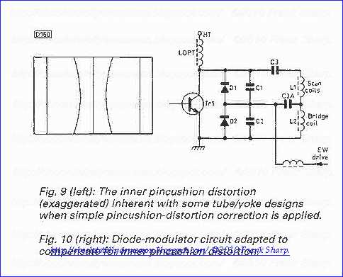 Because
of this. the EW-correction system also has to modulate the S
-correction. Fig. 10 shows, in skeleton circuit form. how this can be
done. There are two coupling/S-correction capacitors. C3 and C3A. C3 is
the usual S -correction capacitor, but C3A has an increasing influence
as the diode modulator begins to have maximum effect towards the centre
of the screen. Critical choice of the value of C3A ensures that the
inner curved verticals shown in Fig. 9 are straightened out to give a
raster completely free from geometric distortion. Although all diode
modulators work on the same basic principle, in some designs a
transformer is used in place of the bridge coil to give better impedance
matching and balance. Fig. 11 shows such an arrangement, used by Bang
and Olufsen. The EW correction waveform is applied to transformer T6.
whose winding 1-2 takes the place of L2 in Figs. 8 and 10. This circuit
also provides inner -pincushion distortion correction as just described,
the supplementary S - correction capacitor being C36.
Because
of this. the EW-correction system also has to modulate the S
-correction. Fig. 10 shows, in skeleton circuit form. how this can be
done. There are two coupling/S-correction capacitors. C3 and C3A. C3 is
the usual S -correction capacitor, but C3A has an increasing influence
as the diode modulator begins to have maximum effect towards the centre
of the screen. Critical choice of the value of C3A ensures that the
inner curved verticals shown in Fig. 9 are straightened out to give a
raster completely free from geometric distortion. Although all diode
modulators work on the same basic principle, in some designs a
transformer is used in place of the bridge coil to give better impedance
matching and balance. Fig. 11 shows such an arrangement, used by Bang
and Olufsen. The EW correction waveform is applied to transformer T6.
whose winding 1-2 takes the place of L2 in Figs. 8 and 10. This circuit
also provides inner -pincushion distortion correction as just described,
the supplementary S - correction capacitor being C36.Diode Modulator Drive

The parabolic EW drive waveform required is easily obtained by feeding the field -scan sawtooth waveform to a double integrator. By adding a sawtooth component the shape of the parabolic waveform can be tilted in either direction to give keystone -distortion correction if required - this is not generally necessary with modern tube/yoke designs. These EW correction characteristics are adjustable by preset resistors or, in the case of bus -programmable sets, remote control commands to the deflection processor. Very often the EW modulator is used to correct the previously mentioned picture breathing effect: this is done by feeding to the EW modulator's control circuit a voltage that's proportional to beam current.
PHILIPS TDA8350Q DC-coupled vertical deflection a
nd East-West output circuit:GENERAL DESCRIPTION
The TDA8350Q is a power circuit for use in 90° and 110°
colour deflection systems for field frequencies of 50
to 120 Hz. The circuit provides a DC driven vertical
deflection output circuit, operating as a highly efficient
class G system and an East-West driver for sinking the
diode modulator current.
FEATURES
• Few external components
• Highly efficient fully DC-coupled vertical output bridge
circuit
• Vertical flyback switch
• Guard circuit
• Protection against:
– short-circuit of the output pins
– short-circuit of the output pins to VP
• High EMC immunity due to common mode inputs
• Temperature (thermal) protection
• East-West output stage with one single conversion
resistor.
FUNCTIONAL DESCRIPTION
The vertical driver circuit is a bridge configuration. The
deflection coil is connected between the output amplifiers,
which are driven in phase opp
osition. An external resistor(RM) connected in series with the deflection coil provides
internal feed back information. The differential input circuit
is voltage driven. The input circuit has been adapted to
enable it to be used with the TDA9150, TDA9151B,
TDA9160A, TDA9162, TDA8366 and TDA8367 which
deliver symmetrical current signals. An external resistor
(RCON) connected between the differential input
determines the output current through the deflection coil.
The relationship between the differential input current and
the output current is defined by: Idiff× RCON= I(coil)× RM.
The output current is adjustable from 0.5 A (p-p) to 3 A
(p-p) by varying RM. The maximum input differential
voltage is 1.8 V. In the application it is recommended that
Vdiff= 1.5 V (typ). This is recommended because of the
spread of input current and the spread in the value of
RCON.
The flyback voltage is determined by an additional supply
voltage VFB. The principle of operating with two supply
voltages (class G) makes it possible to fix the supply
voltage VP optimum for the scan voltage and the second
supply voltage VFB optimum for the flyback voltage. Using
this method, very high efficiency is achieved.
The supply voltage VFB is almost totally available as
flyback voltage across the coil, this being possible due to
the absence of a decoupling capacitor (not necessary, due
to the bridge configuration). The output circuit is fully
protected against the foll
owing:• thermal protection
• short-circuit protection of the output pins (pins 5 and 9)
• short-circuit of the output pins to VP.
A guard circuit VO(guard) is provided. The guard circuit is
activated at the following conditions:
• during flyback
• during various short-circuit possibilities at the output
pins
• during open loop
• when the thermal protection is activated.
This signal can be used for blanking the picture tube
screen.
An East-West amplifier is also provided. This amplifier is
an inverting amplifier which is current driven with sink
current only capabilities.
Notes
1.
A flyback supply voltage of>50 V up to 60 V is allowed in application. A 220 nF capacitor in series with a 22 Ω resistor
(dependent on IO and the inductance of the coil) has to be connected between pin 7 and ground. The decoupling
capacitor of VFB has to be connected between pin 8 and pin 4. This supply voltage line must have a resistance of
33 Ω (see application circuit Fig.5).
2.
IO maximum determined by current protection.
3.
The operating area is limited by a straight line between the points VO(sink)= 40 V; IO(sink)= 10 µA and VO(sink)= 2 V;
IO(sink)= 500 mA.
4.
Up to Vp= 18 V.
Notes
1.
A flyback supply voltage of>50 V up to 60 V is allowed in application. A 220 nF capacitor in series with a 22 Ω resistor
(dependent on IO and the inductance of the coil) has to be connected between pin 7 and ground. The decoupling
capacitor of VFB has to be connected between pin 8 and pin 4. This supply voltage line must have a resistance of
33 Ω (see application circuit Fig.5).
2.
The linearity error is measured without S-correction and based on the same measurement principle as performed on
the screen. The measuring method is as follows:
Divide the output signal I5- I9(VRM) into 22 equal parts ranging from 1 to 22 inclusive. Measure the value of two
succeeding parts called one block starting with part 2 and 3 (block 1) and ending with part 20 and 21 (block 10). Thus
part 1 and 22 are unused. The equations for linearity error for adjacent blocks (LEAB) and not adjacent blocks (NAB)
are given below;
;
3.
Referenced to VP.
4.
V values within formulae, relate to voltages at or between relative pin numbers, i.e. V9-5/V1-2= voltage value across
pins 9 and 5 divided by voltage value across pins 1 and 2.
5.
V3-5 AC short-circuited.
6.
Frequency response V9-5/V3-5 is equal to frequency response V9-5/V1-2.
7.
At V(ripple)= 500 mV eff; measured across RM; fi= 50 Hz.
8.
The output pin 11 requires a capacitor of minimum value 68 nF.
I would like to express my admiration to author for presenting of this amount of knowledge. I too share opinion that for usual enjoyment excellent CRT is perfect. I still use Grundig XS70/1 and I am always amazed how durable is it's picture quality - all settings are in half or less for the best. Sound is also unusuall so I will be unhappy to repalce with new technology - I do not accept TV set to compete with my home reality.
ReplyDelete