


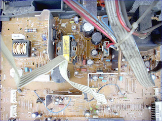
The THOMSON 28DG17E (413/TX807CA) CHASSIS TX807 was first tv color chassis featuring the Ultimate One chip developed by PHILIPS and was the most integrated tv analog chassis at the time with many features and..............light weight.
The
Ultimate One Chip Television provides manufacturers with a single chip,
global TV concept with a wide range of options using advanced proven
technologies for both mixed-signal and digital processes.
By
integrating the core functions of picture and sound decoding, digital
processing and teletext and on-screen display into a single package, the
Ultimate One Chip Television reduces the number of peripheral devices
required. It
allows the manufacturer to design a single chassis for a world family of
television receivers. The same chassis can be used for different size
tubes, for single and multiple transmission standard receivers
(PAL/NTSC/SECAM), and can provide a range of facilities including stereo
sound and different teletext standards.
The analog circuitry, built in Philips' BiMOS process technology, is
primarily concerned with the colour decoding and other picture and sound
processing. The digital circuitry, built with Philips' CMOS technology,
looks after on screen display using a microprocessor core and
specialist caption decoder and teletext circuitry. Also included as part
of the digital circuitry is one time programmable (OTP) memory and up
to 2K RAM. The process technologies are both regarded as amongst the
most advanced in the industry, providing higher levels of integration
and lower levels of power consumption than competitive processes.
THOMSON 28DG17E (413/TX807CS) CHASSIS TX807 BACKGROUND OF THE INVENTION:
1. Field of Invention The present invention relates to television technology, and more particularly to providing television functionality on a single integrated circuit chip.
2. Background
Television systems have become increasingly complex as consumers continue to demand greater functionality and performance from television sets. Furthermore, the miniaturization of television systems demands that while complexity is increasing, that the size of electronic circuitry to support this complexity and performance must be reduced. At the same time, market forces continue to drive prices lower for television sets. Current electronic circuitry to support the functionality needed to receive audio and video signals that are either analog or digital and process those signals to provide a signal suitable for display on a television often consist of several integrated circuits. Furthermore, additional functionality related to value added features, such as teletext or e-commerce often requires additional integrated circuits.
What is needed is a system for providing television functionality and ancillary functionality on a single integrated chip to reduce costs and support the continued miniaturization of electronics for televisions.
The present invention
provides a cost effective approach for implementing television
functionality on a single integrated circuit chip (referred to herein as
“TV on a Chip” or TVOC). A TVOC includes functionality to receive and
display television signals in a variety of input and output formats. A
TVOC can be used in set-top boxes for cable and satellite television, or
directly within a television. All or substantially all functionality
provided can be provided on a single integrated circuit. TVOC includes
one or more of a data transport module, an IF demodulator, a digital
audio engine, an analog audio engine, a digital video engine, and an
analog video engine. The TVOC also includes three sets of interfaces
including output interfaces, control interfaces and ancillary
interfaces. The present invention addresses the conflicting consumer demands of television system miniaturization and reducing the cost of televisions.
THOMSON 28DG17E (413/TX807CS) CHASSIS TX807 Power supply with ecological stand by mode:
The switched mode power supply according to the invention comprises a
circuit 30 whose function is to reduce in an ecological stand by mode
voltage output at secondary 40 of a transformer 2 of the power supply,
at a minimum necessary to supply a microprocessor of an electronic
appliance in which the supply is included. In a preferred embodiment
circuit 30 is included in a feedback loop 15 from a secondary output of
the transformer 2, to polarising means 17, 29 of a switching transistor
14. The effect of circuit 30 is then to reduce time ON of said
transistor 14, leading to less output energy at the secondary of
transformer 2.
 1. Switched mode power supply of an electronic appliance, the
power supply being capable of at least two working modes, a stand by
mode and a normal mode, the power supply being fitted with a transformer
(2) having primary and secondary windings, the primary windings of the
transformer being connectable to a direct current source (1), switching
active electronic means (14) having a drive electrode (16) fitted with
polarisation means (29, 17), the switching means (14) causing when they
are switched ON, a current to flow through the primary windings (3) of
the transformer (2), the secondary windings of the transformer (2) being
coupled to rectifying and smoothing means (4, 5, 8) to deliver output
voltages that are needed for different circuits of the appliance, power
supply wherein a time ON shortening circuit (30) is coupled to the
polarisation means (29, 17) of the driving electrode (16) of the
switching means (14) whose function is to settle one output voltages
from a higher value in normal mode to a lower value in stand by mode.
1. Switched mode power supply of an electronic appliance, the
power supply being capable of at least two working modes, a stand by
mode and a normal mode, the power supply being fitted with a transformer
(2) having primary and secondary windings, the primary windings of the
transformer being connectable to a direct current source (1), switching
active electronic means (14) having a drive electrode (16) fitted with
polarisation means (29, 17), the switching means (14) causing when they
are switched ON, a current to flow through the primary windings (3) of
the transformer (2), the secondary windings of the transformer (2) being
coupled to rectifying and smoothing means (4, 5, 8) to deliver output
voltages that are needed for different circuits of the appliance, power
supply wherein a time ON shortening circuit (30) is coupled to the
polarisation means (29, 17) of the driving electrode (16) of the
switching means (14) whose function is to settle one output voltages
from a higher value in normal mode to a lower value in stand by mode.
2. Switched mode power supply according to claim 1 wherein the time ON shortening circuit (30) has an input (35) and an output (36), said output (36) having two states, a first when the power supply is in normal mode and a second when the power supply is in the stand by mode, said second state having as an effect to shorten time ON of the switching transistor.
3. Switched mode power supply according to claim 2 wherein said input (35) of said time ON shortening circuit (30) is coupled to a first terminal (31) of the secondary (40) of the transformer (2).
4. Switched mode power supply according to claim 3 wherein said output (36) of said time ON shortening circuit (30) is coupled to a second terminal (24) of the secondary (40) of the transformer (2).
5. Switched mode power supply according to claim 4 wherein said first terminal (31) of the transformer (2). at which said input (35) of said tim
e ON shortening circuit (30) is coupled, has, in
normal mode a higher voltage output than the one of said second terminal
(24) of the secondary (40) of the transformer (2) ). at which said
output (36) of said time ON shortening circuit (30) is coupled, and in
standby mode, a lower voltage output than the one at which said output
(36) of said time ON shortening circuit is coupled. 6. Switched mode power supply according to claim 5 wherein the time ON shortening circuit (30) comprises a rectifying mean (33) connected in Series with a resistor (34).
Description:
Field of the invention
The invention relates to a switched mode power supply having a stand by mode, during which the electric power consumption is reduced. Background of the invention
In a switched mode power supply, such for instance as the one represented in figure 1, a direct current source 1 is applied to the main path of a switching means, for instance a Field Effect Transistor 14 (FET). When switching MOSFET is ON a current is flooding from direct current source 1 through a primary winding 3 of a flyback transformer 2 and across a drain 37 to a source 38 of said transistor 14 and across a resistor 28 to primary ground. In a known way the resulting pulsed current applied to primary winding 3 of forward or flyback transformer 2 is producing a pulsed current at the secondary 40 of transformer 2.
After rectification by rectifiers 4, 5, 6, 7 and smoothing by filter circuits such as circuit 8, voltage of different values coming from secondary windings 9, 10, 11, and from taps 12, 13, of those secondary windings are applied to loads not repres ented of an electronic appliance, for
instance a video tape recorder (VCR) or a television set (TV) or others.
The ratio of the ON time of the FET 14 relative to the total switching
period of the FET 14 is controlled by a feedback loop 15. The feedback
loop 15 is taken from one or a combination of the voltages at the output
of a smoothed and rectified secondary of the transformer 2. The power
supply has different modes of working. As examples it will be cited
there after a normal mode and a stand by mode.
ented of an electronic appliance, for
instance a video tape recorder (VCR) or a television set (TV) or others.
The ratio of the ON time of the FET 14 relative to the total switching
period of the FET 14 is controlled by a feedback loop 15. The feedback
loop 15 is taken from one or a combination of the voltages at the output
of a smoothed and rectified secondary of the transformer 2. The power
supply has different modes of working. As examples it will be cited
there after a normal mode and a stand by mode.
The normal mode is a mode in which the appliance being ON, the power supply delivers the average power which is needed for the appliance to work properly. In the stand by mode the appliance is OFF, but a part of it is still powered. In electronic appliances such as TV and VCR it is the receiver for a remote control of the appliance. Said remote control receiver must be able first to reset a microprocessor for control of the appliance, said microprocessor when reset having a software to progressively revive the power supply up to the point where it will be delivering a sufficient power for the functions of the appliance that have been revived. In general said microprocessor must be fed with a 5 volts minimum voltage to be able of being reset.
 In general also the voltage at the
output of the power supply delivering what is called the 5 volts supply
is greater than 5 volts for instance 5,3 volts so that with the voltages
drops along the copper lines and switches the voltages at the inputs of
circuits needing a minimum 5 volts voltage is still above 5 volts.
Summary of the invention.
In general also the voltage at the
output of the power supply delivering what is called the 5 volts supply
is greater than 5 volts for instance 5,3 volts so that with the voltages
drops along the copper lines and switches the voltages at the inputs of
circuits needing a minimum 5 volts voltage is still above 5 volts.
Summary of the invention.
The purpose of the invention is to lower the power consumption in stand by mode. The output power is the products of output currents and output voltages. Reduction of either current or voltage on the output lines of the secondary windings delivering the needed voltages for instance 5V, 14V, 33V, 27V...etc. will be able to cut down the output power, hence reducing the input power. The voltage which is required at the output of a secondary winding of transformer 2, is equal to the minimum voltage which is required at the input of a circuit fed by said voltage, increased with the maximum drops of voltage that may occur between said output and said input. If there are several circuits that are to be fed from the same output of the transformer, then the minimum voltage to be set at said output, is the bigger value of the different minimum values needed for each of the circuit.
 It may happen, and it is often the case, that
a circuit which is needed to be fed in normal mode need not be fed in
stand by mode. If it is the case, and if the minimum output voltage
which is needed for said not needed in stand by mode circuit leads to a
voltage which is higher than all the ones which are needed in stand by
mode, then in stand by mode there is a margin to reduce said voltage,
and then to reduce consumption in this mode. Of course in such a case
and to take advantage of this margin, the power supply must be fitted
with a circuit that will enable the power supply to deliver on at least
one of its outputs a lower voltage during stand by mode than during
normal run mode.
It may happen, and it is often the case, that
a circuit which is needed to be fed in normal mode need not be fed in
stand by mode. If it is the case, and if the minimum output voltage
which is needed for said not needed in stand by mode circuit leads to a
voltage which is higher than all the ones which are needed in stand by
mode, then in stand by mode there is a margin to reduce said voltage,
and then to reduce consumption in this mode. Of course in such a case
and to take advantage of this margin, the power supply must be fitted
with a circuit that will enable the power supply to deliver on at least
one of its outputs a lower voltage during stand by mode than during
normal run mode.
To sum up the invention is about a switched mode power supply of an electronic appliance the appliance having different circuits that may or may not be powered according to a mode of control of the appliance, the power supply being capable of at least two modes, a first one being a stand by mode in which only some of the circuit are powered and a second being a normal mode in which the circuits of the appliance are fed in accordance with a normal working of the appliance, the power supply being fitted with a transformer having primary and secondary windings, the primary windings of the transformer being connectable to a direct current source, switching active electronic means having a drive electrode fitted with polarisation means, the switching means causing when they are switched ON, a current to flow through the primary windings of the transformer,
 the secondary
windings of the transformer being coupled to rectifying and smoothing
means to deliver output voltages that are needed for the different
circuits of the appliance, one at least of the delivered voltages being
to feed at least 2 different circuits, a first and a second, the first
one being powered in normal mode and not powered in stand by mode, said
first one requiring the output voltage to be settled at a higher voltage
than the second circuit, said second circuit being powered in the
normal and in the stand-by mode, power supply wherein a time ON
shortening circuit is coupled to the polarisation means of the driving
electrode of the switching means whose function is to bring back said
one at least output voltage from a higher value in normal mode to a
lower value in stand by mode, said lower value being the one which is
needed to supply the second circuit.
the secondary
windings of the transformer being coupled to rectifying and smoothing
means to deliver output voltages that are needed for the different
circuits of the appliance, one at least of the delivered voltages being
to feed at least 2 different circuits, a first and a second, the first
one being powered in normal mode and not powered in stand by mode, said
first one requiring the output voltage to be settled at a higher voltage
than the second circuit, said second circuit being powered in the
normal and in the stand-by mode, power supply wherein a time ON
shortening circuit is coupled to the polarisation means of the driving
electrode of the switching means whose function is to bring back said
one at least output voltage from a higher value in normal mode to a
lower value in stand by mode, said lower value being the one which is
needed to supply the second circuit.
 Said in a different way, not
pointing out what the interest of the invention is, the invention is
about a switched mode power supply of an electronic appliance, the power
supply being capable of at least two working modes, a stand by mode and
a normal mode, the power supply being fitted with a transformer having
primary and secondary windings, the primary windings of the transformer
being connectable to a direct current source, switching active
electronic means having a drive electrode fitted with polarisation
means, the switching means causing when they are switched ON, a current
to flow through the primary windings of the transformer, the secondary
windings of the transformer being coupled to rectifying and smoothing
means to deliver output voltages that are needed for different circuits
of the appliance,
Said in a different way, not
pointing out what the interest of the invention is, the invention is
about a switched mode power supply of an electronic appliance, the power
supply being capable of at least two working modes, a stand by mode and
a normal mode, the power supply being fitted with a transformer having
primary and secondary windings, the primary windings of the transformer
being connectable to a direct current source, switching active
electronic means having a drive electrode fitted with polarisation
means, the switching means causing when they are switched ON, a current
to flow through the primary windings of the transformer, the secondary
windings of the transformer being coupled to rectifying and smoothing
means to deliver output voltages that are needed for different circuits
of the appliance,
power supply wherein a time ON shortening circuit is coupled to the polarisation means of the driving electrode of the switching means whose function is to shorten time ON of said switching means then settling one output voltage from a higher value in normal mode to a lower value in stand by mode.
The action of the time ON shortening circuit is to shorten the time ON of the switching transistor. So, although the lowering of the output voltages is settled to a minimum value which is needed for instance for the microprocessor, that is to say one of the circuits, the fact that said lowering of said voltage is got by shortening time ON, of the switching means, will have a lowering effect on all the output voltages. That will contribute to the lowering of the electrical consumption of electrical power in stand by mode.
In the preferred embodiment of the invention the time ON shortening circuit has an input coupled to one of the terminals delivering an output voltage, and an input coupled to the drive electrode. That means that the time ON shortening circuit is in a feedback loop of the power supply. Brief description of the drawings.
An embodiment of the invention will now be described in accordance with the appended drawings in which: Figure 1 which has already been partially commented is a circuit diagramof a power supply according to
the invention. Figure 2 is a set of characteristic curves of a zener
diode which is used to explain how the invention is working.
Coming back to figure 1, it has already been explained that power transmitted from the primary of transformer 2 to secondary 40 of said transformer is depending upon time ON of switching transistor 14. The duration of ON time is depending upon the value of a voltage at the gate 16 of MOSFET 14, said voltage being in direct relation with voltage at the ends of capacitors 26, whose charging circuit is under control of transistors 17 and 18. The base 19 of transistor 18 is under control of a photo coupler 20 that bring back with galvanic insulation a feedback current from the secondary side. Primary side and secondary side of the transformer are often referred to as hot and cold side of the power supply. On the cold side photo coupler 20 is fed through a transistor 21.
Capacitor 26, transistor 17, 18, photo coupler 20 and transistor 21 are the main components of a feedback loop 15.
The working of said feedback loop will now be explained. Transistor 21 has its base 22, polarised by mean of a zener diode 23. The polarising voltage of base 22 is depending upon the value of a current going from a terminal 24 of a secondary winding of transformer 2. If for any reason there is for instance, a lower current is flooding from terminal 24 through zener diode 23, the drop of voltage due to zener diode 23 is reduced. See the characteristic of zener diode 23 in figure 2. That means that polarising voltage at the base 22 of transistor 21 is reduced. In the case represented in figure 1 transistor 21 is a PNP small signal transistor. With a smaller base voltage it will be allowed to be turn ON for a longer time and this will allow more collector current to flow through transistor 21. That means that more current is directed toward the cold side of photo coupler 20.
More current in cold side of photo coupler 20 means also more current at the hot side. Said current of the hot side is added to current coming from drain 37 to source 38 of transistor 14 and to a resistor 39 to polarise at a higher level the base 19 of a transistor 18. Then the polarisation of transistor 18 is settled to a higher level. That allows transistor 18 which in this case is a NPN transistor to be ON for a longer time. The collector emitter path of transistor 18 is connected to the base 27 of transistor 17. So in turn transistor 17 will be ON a longer time. The collector emitter path of transistor 18 is bypassing polarising resistor 29 of the gate 16 of switching transistor 14, and then pulling to low said gate 16. The longer said gate 16 is pulled to low the shorter said MOSFET transistor 14 is ON.
Then to make a long story short, if a
current higher than a predetermined value is detected at a terminal 24
of a winding of the secondary side, a feedback loop 15 is activated and
the time ON of MOSFET 14 is reduced. Said feedback loop is controlling
the polarisation means, here transistor 17 that bypass polarising
resistor of the gate 16 of MOSFET 14. It is to be noted that in a strict
sense polarising means of MOSFET 14 is resistor 29. In the case of a
transistor which is normally working with a permanent succession of ON
and OFF states it may be considered in this application that transistor
17 which is bypassing said resistor 29 in order to reduce voltage at
gate 16 under the minimum needed for the transistor to be ON, is also a
part of the polarising means. The feedback loop 15 and the way it is
working that has been described up to now is a normal and known feedback
loop.
An example of a circuit which may be added to arrive at a power supply according to the invention will now be described.
The added circuit according to the invention is referred to as 30 on figure 1. Circuit 30 is connected between a terminal 31 at a tap 31 of a secondary winding of transformer 2, and the cathode 32 of zener diode 23. Circuit 30 is made of a diode 33 and of a resistor 34 connected in series. The tap 31 at which an input 35 of circuit 30 is connected is in normal operation mode, fed with a voltage which is higher than the voltage at the terminal 24 which is the starting point of feedback loop 15. The output 36 of circuit 30 is as already said connected to cathode 32 of diode 23, said cathode 32 being also coupled via a resistor to terminal 24 of transformer 2. The fact that terminal 31 is in normal mode at a higher voltage than terminal 24 means that in normal mode a current is flooding through diode 33 of circuit 30 toward Zener diode 23.
Said current is flooding through said diode 23 and hence according to the characteristic of figure 2 said additional current in zener diode means a higher drop of voltage. What has been explained up to now about circuit 30 means that in normal mode the drop of voltage at the base 22 of transistor 21 is due to an addition of two currents in said zener diode one coming from terminal 24 and one coming from terminal 31. As has been
 explained above, time ON and OFF of switching
MOSFET 14 is determined by the polarisation of transistor 21. The
adjusting of said polarisation for normal mode must take in account the
effect of circuit 30 and of the added current.
explained above, time ON and OFF of switching
MOSFET 14 is determined by the polarisation of transistor 21. The
adjusting of said polarisation for normal mode must take in account the
effect of circuit 30 and of the added current.
Tap 31 has been chosen because in stand by mode, terminal 31 is OFF. No current is going anymore through diode 33 of circuit 30. One of the two currents to settle the drop of voltage at the base 22 of transistor 21 is missing, and then as explained above in relation with the description of prior art working of loop 15, time ON of MOSFET 14 will be reduced leading to a reduced voltage output on every terminal or tap of the secondary windings 40 of transformer 2. In particular 5 volts only generated and just enough to supply the microprocessor. Less energy is being transferred to the secondary 40 of the transformer.
In a realisation of a switched mode power supply according to the preferred embodiment the following results have been achieved: Less energy is transferred in stand by mode to the secondary side as a consequence of
the following reductions of voltage: 5.3VE level reduced from 5.3V to
5.1V. 14VE level reduced from 14.5V to 12V. -27VE level reduce from -27V
to -22.5V 33VE level reduced from 33V to 26V. 4.2V level reduced from
4.2V to 2.9V.
End result, input power measured, reduced about 1 W or 22% from 4.5W to 3.5W during a standby mode that is now called ecological stand by mode.
The embodiment of the invention that has just been described is a very simple and cost effective one. It has the advantage to be fully automatic, and to settle the feedback loop in a new state that will reduce voltage outputs as soon as the stand by mode is settled. However it can be seen that any circuit that would be coupled to the controlling circuit 17 of gate 16 of MOSFET 14, said circuit having two output states a first for normal mode and a second for stand by mode, the second state of circuit 30 triggering ON transistor 17 which is bypassing polarisation resistor 29 of driving electrode 16.
In a more general way any circuit coupled to polarising means of a drive electrode and having a first output state in normal mode and a second one in stand by mode said second state reducing time ON of the transistor would be a time ON shortening circuit as circuit 30 of the above embodiment.
THOMSON TDA8139 5.1V AND ADJUSTABLE VOLTAGE REGULATOR WITH DISABLE AND RESET:
DESCRIPTI ON
ON
The TDA8139 is a monolithic dual positive voltage
regulator designed to provide precision output volt-
ages of 5.1V and adjustable at currents up to
750mA.
An internal reset circuit generates a reset pulse
when the output 1 decrease below the regulated
voltage value.
Output 2 can be disabled by TTL input.
Short circuit and thermal protections are included.
.FIXED PRECISION OUTPUT 1 VOLTAGE
5.1V ± 2%
.OUTPUT 2 VOLTAGE PROGRAMMABLE
FROM 2.8 TO 16V
.OUTPUT 1 WITH RESET FACILITY
.OUTPUT 2 WITH DISABLE BY TTL INPUT
.SHORT CIRCUIT PROTECTION AT BOTH
OUTPUTS
.THERMAL PROTECTION
.LOW DROP OUTPUT VOLTAGE.
 CIRCUIT DESCRIPTION
The TDA8139 is a dual voltage regulator with Reset
and Disable.
The two regulation parts are supplied from one
voltage reference circuit trimmed by zener zap
during EWS test. Since the supply voltage of this
last is connected at Pin 1 (VIN1), the regulator 2 will
not work if the Pin 1 is not supplied.
The outputs stages have been realized in dar-
lington configuration with a drop typical of 1.2V.
The disable circuit, switch-off the output 2 if a
voltage lower than 0.8V is applied at pin 4.
The Reset circuit checks the voltage at the output
1. If this one goes below VOUT - 0.25V (4.85V Typ.),
the comparator "a" (see Figure 1) discharges rap-
idly the capacitor Ce and the reset output goes at
once low. When the voltage at the OUT 1 rises
above VOUT -0.2V (4.9V Typ.), the voltage VCe
increases linearly to 2.5V corresponding to a delay
td following the low : td = Ce ⋅ 2.5V
10µA
(see figure 2),
then the reset output goes high again. To avoid
glitches in the reset output, the second comparator
"b" has a large hysteresis (1.9V).
THOMSON TDA9302H VERTICALDEFLECTION OUTPUT CIRCUIT:
DESCRIPTION
The TDA9302H is a monolithic integrated circuit in
HEPTAWATT TM package. It is a high efficiency
power boosterfordirectdriving of verticalwindings
of TV yokes. It is intendedfor use in Color andB &
W television as well as in monitorsand displays.
.FLYBACK GENERATOR
.THERMAL PROTECTION
MOUNTING INSTRUCTIONS
The power dissipated in the circuit must be re-
moved by adding an externalheatsink.
Thanks to the HEPTAWATTTMpackage attaching
the heatsinkis very simple, a screw or a compres-
sion spring (clip) being sufficient.
Between the heatsink and the package it is better
to insert a layer of silicon grease, to optimize the
thermal contact ; no electrical isolation is needed
between the two surfaces, since the tab is con-
nected to Pin 4 which is ground.
The invention relates to a switched mode power supply having a stand by mode, during which the electric power consumption is reduced. Background of the invention
In a switched mode power supply, such for instance as the one represented in figure 1, a direct current source 1 is applied to the main path of a switching means, for instance a Field Effect Transistor 14 (FET). When switching MOSFET is ON a current is flooding from direct current source 1 through a primary winding 3 of a flyback transformer 2 and across a drain 37 to a source 38 of said transistor 14 and across a resistor 28 to primary ground. In a known way the resulting pulsed current applied to primary winding 3 of forward or flyback transformer 2 is producing a pulsed current at the secondary 40 of transformer 2.
After rectification by rectifiers 4, 5, 6, 7 and smoothing by filter circuits such as circuit 8, voltage of different values coming from secondary windings 9, 10, 11, and from taps 12, 13, of those secondary windings are applied to loads not repres
ented of an electronic appliance, for
instance a video tape recorder (VCR) or a television set (TV) or others.
The ratio of the ON time of the FET 14 relative to the total switching
period of the FET 14 is controlled by a feedback loop 15. The feedback
loop 15 is taken from one or a combination of the voltages at the output
of a smoothed and rectified secondary of the transformer 2. The power
supply has different modes of working. As examples it will be cited
there after a normal mode and a stand by mode.The normal mode is a mode in which the appliance being ON, the power supply delivers the average power which is needed for the appliance to work properly. In the stand by mode the appliance is OFF, but a part of it is still powered. In electronic appliances such as TV and VCR it is the receiver for a remote control of the appliance. Said remote control receiver must be able first to reset a microprocessor for control of the appliance, said microprocessor when reset having a software to progressively revive the power supply up to the point where it will be delivering a sufficient power for the functions of the appliance that have been revived. In general said microprocessor must be fed with a 5 volts minimum voltage to be able of being reset.
In general also the voltage at the
output of the power supply delivering what is called the 5 volts supply
is greater than 5 volts for instance 5,3 volts so that with the voltages
drops along the copper lines and switches the voltages at the inputs of
circuits needing a minimum 5 volts voltage is still above 5 volts.
Summary of the invention.The purpose of the invention is to lower the power consumption in stand by mode. The output power is the products of output currents and output voltages. Reduction of either current or voltage on the output lines of the secondary windings delivering the needed voltages for instance 5V, 14V, 33V, 27V...etc. will be able to cut down the output power, hence reducing the input power. The voltage which is required at the output of a secondary winding of transformer 2, is equal to the minimum voltage which is required at the input of a circuit fed by said voltage, increased with the maximum drops of voltage that may occur between said output and said input. If there are several circuits that are to be fed from the same output of the transformer, then the minimum voltage to be set at said output, is the bigger value of the different minimum values needed for each of the circuit.
It may happen, and it is often the case, that
a circuit which is needed to be fed in normal mode need not be fed in
stand by mode. If it is the case, and if the minimum output voltage
which is needed for said not needed in stand by mode circuit leads to a
voltage which is higher than all the ones which are needed in stand by
mode, then in stand by mode there is a margin to reduce said voltage,
and then to reduce consumption in this mode. Of course in such a case
and to take advantage of this margin, the power supply must be fitted
with a circuit that will enable the power supply to deliver on at least
one of its outputs a lower voltage during stand by mode than during
normal run mode.To sum up the invention is about a switched mode power supply of an electronic appliance the appliance having different circuits that may or may not be powered according to a mode of control of the appliance, the power supply being capable of at least two modes, a first one being a stand by mode in which only some of the circuit are powered and a second being a normal mode in which the circuits of the appliance are fed in accordance with a normal working of the appliance, the power supply being fitted with a transformer having primary and secondary windings, the primary windings of the transformer being connectable to a direct current source, switching active electronic means having a drive electrode fitted with polarisation means, the switching means causing when they are switched ON, a current to flow through the primary windings of the transformer,
the secondary
windings of the transformer being coupled to rectifying and smoothing
means to deliver output voltages that are needed for the different
circuits of the appliance, one at least of the delivered voltages being
to feed at least 2 different circuits, a first and a second, the first
one being powered in normal mode and not powered in stand by mode, said
first one requiring the output voltage to be settled at a higher voltage
than the second circuit, said second circuit being powered in the
normal and in the stand-by mode, power supply wherein a time ON
shortening circuit is coupled to the polarisation means of the driving
electrode of the switching means whose function is to bring back said
one at least output voltage from a higher value in normal mode to a
lower value in stand by mode, said lower value being the one which is
needed to supply the second circuit.Said in a different way, not
pointing out what the interest of the invention is, the invention is
about a switched mode power supply of an electronic appliance, the power
supply being capable of at least two working modes, a stand by mode and
a normal mode, the power supply being fitted with a transformer having
primary and secondary windings, the primary windings of the transformer
being connectable to a direct current source, switching active
electronic means having a drive electrode fitted with polarisation
means, the switching means causing when they are switched ON, a current
to flow through the primary windings of the transformer, the secondary
windings of the transformer being coupled to rectifying and smoothing
means to deliver output voltages that are needed for different circuits
of the appliance,power supply wherein a time ON shortening circuit is coupled to the polarisation means of the driving electrode of the switching means whose function is to shorten time ON of said switching means then settling one output voltage from a higher value in normal mode to a lower value in stand by mode.
The action of the time ON shortening circuit is to shorten the time ON of the switching transistor. So, although the lowering of the output voltages is settled to a minimum value which is needed for instance for the microprocessor, that is to say one of the circuits, the fact that said lowering of said voltage is got by shortening time ON, of the switching means, will have a lowering effect on all the output voltages. That will contribute to the lowering of the electrical consumption of electrical power in stand by mode.
In the preferred embodiment of the invention the time ON shortening circuit has an input coupled to one of the terminals delivering an output voltage, and an input coupled to the drive electrode. That means that the time ON shortening circuit is in a feedback loop of the power supply. Brief description of the drawings.
An embodiment of the invention will now be described in accordance with the appended drawings in which: Figure 1 which has already been partially commented is a circuit diagram
of a power supply according to
the invention. Figure 2 is a set of characteristic curves of a zener
diode which is used to explain how the invention is working.Coming back to figure 1, it has already been explained that power transmitted from the primary of transformer 2 to secondary 40 of said transformer is depending upon time ON of switching transistor 14. The duration of ON time is depending upon the value of a voltage at the gate 16 of MOSFET 14, said voltage being in direct relation with voltage at the ends of capacitors 26, whose charging circuit is under control of transistors 17 and 18. The base 19 of transistor 18 is under control of a photo coupler 20 that bring back with galvanic insulation a feedback current from the secondary side. Primary side and secondary side of the transformer are often referred to as hot and cold side of the power supply. On the cold side photo coupler 20 is fed through a transistor 21.
Capacitor 26, transistor 17, 18, photo coupler 20 and transistor 21 are the main components of a feedback loop 15.
The working of said feedback loop will now be explained. Transistor 21 has its base 22, polarised by mean of a zener diode 23. The polarising voltage of base 22 is depending upon the value of a current going from a terminal 24 of a secondary winding of transformer 2. If for any reason there is for instance, a lower current is flooding from terminal 24 through zener diode 23, the drop of voltage due to zener diode 23 is reduced. See the characteristic of zener diode 23 in figure 2. That means that polarising voltage at the base 22 of transistor 21 is reduced. In the case represented in figure 1 transistor 21 is a PNP small signal transistor. With a smaller base voltage it will be allowed to be turn ON for a longer time and this will allow more collector current to flow through transistor 21. That means that more current is directed toward the cold side of photo coupler 20.
More current in cold side of photo coupler 20 means also more current at the hot side. Said current of the hot side is added to current coming from drain 37 to source 38 of transistor 14 and to a resistor 39 to polarise at a higher level the base 19 of a transistor 18. Then the polarisation of transistor 18 is settled to a higher level. That allows transistor 18 which in this case is a NPN transistor to be ON for a longer time. The collector emitter path of transistor 18 is connected to the base 27 of transistor 17. So in turn transistor 17 will be ON a longer time. The collector emitter path of transistor 18 is bypassing polarising resistor 29 of the gate 16 of switching transistor 14, and then pulling to low said gate 16. The longer said gate 16 is pulled to low the shorter said MOSFET transistor 14 is ON.
Then to make a long story short, if a
current higher than a predetermined value is detected at a terminal 24
of a winding of the secondary side, a feedback loop 15 is activated and
the time ON of MOSFET 14 is reduced. Said feedback loop is controlling
the polarisation means, here transistor 17 that bypass polarising
resistor of the gate 16 of MOSFET 14. It is to be noted that in a strict
sense polarising means of MOSFET 14 is resistor 29. In the case of a
transistor which is normally working with a permanent succession of ON
and OFF states it may be considered in this application that transistor
17 which is bypassing said resistor 29 in order to reduce voltage at
gate 16 under the minimum needed for the transistor to be ON, is also a
part of the polarising means. The feedback loop 15 and the way it is
working that has been described up to now is a normal and known feedback
loop.An example of a circuit which may be added to arrive at a power supply according to the invention will now be described.
The added circuit according to the invention is referred to as 30 on figure 1. Circuit 30 is connected between a terminal 31 at a tap 31 of a secondary winding of transformer 2, and the cathode 32 of zener diode 23. Circuit 30 is made of a diode 33 and of a resistor 34 connected in series. The tap 31 at which an input 35 of circuit 30 is connected is in normal operation mode, fed with a voltage which is higher than the voltage at the terminal 24 which is the starting point of feedback loop 15. The output 36 of circuit 30 is as already said connected to cathode 32 of diode 23, said cathode 32 being also coupled via a resistor to terminal 24 of transformer 2. The fact that terminal 31 is in normal mode at a higher voltage than terminal 24 means that in normal mode a current is flooding through diode 33 of circuit 30 toward Zener diode 23.
Said current is flooding through said diode 23 and hence according to the characteristic of figure 2 said additional current in zener diode means a higher drop of voltage. What has been explained up to now about circuit 30 means that in normal mode the drop of voltage at the base 22 of transistor 21 is due to an addition of two currents in said zener diode one coming from terminal 24 and one coming from terminal 31. As has been

Tap 31 has been chosen because in stand by mode, terminal 31 is OFF. No current is going anymore through diode 33 of circuit 30. One of the two currents to settle the drop of voltage at the base 22 of transistor 21 is missing, and then as explained above in relation with the description of prior art working of loop 15, time ON of MOSFET 14 will be reduced leading to a reduced voltage output on every terminal or tap of the secondary windings 40 of transformer 2. In particular 5 volts only generated and just enough to supply the microprocessor. Less energy is being transferred to the secondary 40 of the transformer.
In a realisation of a switched mode power supply according to the preferred embodiment the following results have been achieved: Less energy is transferred in stand by mode to the secon
dary side as a consequence of
the following reductions of voltage: 5.3VE level reduced from 5.3V to
5.1V. 14VE level reduced from 14.5V to 12V. -27VE level reduce from -27V
to -22.5V 33VE level reduced from 33V to 26V. 4.2V level reduced from
4.2V to 2.9V.End result, input power measured, reduced about 1 W or 22% from 4.5W to 3.5W during a standby mode that is now called ecological stand by mode.
The embodiment of the invention that has just been described is a very simple and cost effective one. It has the advantage to be fully automatic, and to settle the feedback loop in a new state that will reduce voltage outputs as soon as the stand by mode is settled. However it can be seen that any circuit that would be coupled to the controlling circuit 17 of gate 16 of MOSFET 14, said circuit having two output states a first for normal mode and a second for stand by mode, the second state of circuit 30 triggering ON transistor 17 which is bypassing polarisation resistor 29 of driving electrode 16.
In a more general way any circuit coupled to polarising means of a drive electrode and having a first output state in normal mode and a second one in stand by mode said second state reducing time ON of the transistor would be a time ON shortening circuit as circuit 30 of the above embodiment.
THOMSON TDA8139 5.1V AND ADJUSTABLE VOLTAGE REGULATOR WITH DISABLE AND RESET:
DESCRIPTI
ONThe TDA8139 is a monolithic dual positive voltage
regulator designed to provide precision output volt-
ages of 5.1V and adjustable at currents up to
750mA.
An internal reset circuit generates a reset pulse
when the output 1 decrease below the regulated
voltage value.
Output 2 can be disabled by TTL input.
Short circuit and thermal protections are included.
.FIXED PRECISION OUTPUT 1 VOLTAGE
5.1V ± 2%
.OUTPUT 2 VOLTAGE PROGRAMMABLE
FROM 2.8 TO 16V
.OUTPUT 1 WITH RESET FACILITY
.OUTPUT 2 WITH DISABLE BY TTL INPUT
.SHORT CIRCUIT PROTECTION AT BOTH
OUTPUTS
.THERMAL PROTECTION
.LOW DROP OUTPUT VOLTAGE.
CIRCUIT DESCRIPTIONThe TDA8139 is a dual voltage regulator with Reset
and Disable.
The two regulation parts are supplied from one
voltage reference circuit trimmed by zener zap
during EWS test. Since the supply voltage of this
last is connected at Pin 1 (VIN1), the regulator 2 will
not work if the Pin 1 is not supplied.
The outputs stages have been realized in dar-
lington configuration with a drop typical of 1.2V.
The disable circuit, switch-off the output 2 if a
voltage lower than 0.8V is applied at pin 4.
The Reset circuit checks the voltage at the output
1. If this one goes below VOUT - 0.25V (4.85V Typ.),
the comparator "a" (see Figure 1) discharges rap-
idly the capacitor Ce and the reset output goes at
once low. When the voltage at the OUT 1 rises
above VOUT -0.2V (4.9V Typ.), the voltage VCe
increases linearly to 2.5V corresponding to a delay
td following the low : td = Ce ⋅ 2.5V
10µA
(see figure 2),
then the reset output goes high again. To avoid
glitches in the reset output, the second comparator
"b" has a large hysteresis (1.9V).
THOMSON TDA9302H VERTICALDEFLECTION OUTPUT CIRCUIT:
DESCRIPTION
The TDA9302H is a monolithic integrated circuit in
HEPTAWATT TM package. It is a high efficiency
po
wer boosterfordirectdriving of verticalwindingsof TV yokes. It is intendedfor use in Color andB &
W television as well as in monitorsand displays.
.FLYBACK GENERATOR
.THERMAL PROTECTION
MOUNTING INSTRUCTIONSThe power dissipated in the circuit must be re-
moved by adding an externalheatsink.
Thanks to the HEPTAWATTTMpackage attaching
the heatsinkis very simple, a screw or a compres-
sion spring (clip) being sufficient.
Between the heatsink and the package it is better
to insert a layer of silicon grease, to optimize the
thermal contact ; no electrical isolation is needed
between the two surfaces, since the tab is con-
nected to Pin 4 which is ground.
THOMSON 28DG17E (413/TX807CS) CHASSIS TX807 PHILIPS TDA9554PS/N1/1/0301 CZ9749 KOG160 IVV 2.20 series TV signal processor-Teletext decoder with embedded µ-Controller:
GENERAL DESCRIPTIONcombine the functions of a video processor together with a
µ-Controller and US Closed Caption decoder. Several
versions have a Teletext decoder on board. The Teletext
decoder has an internal RAM memory for 1or 10 page text.
The ICs are intended to be used in economy television
receivers with 90° and 110° picture tubes.
The ICs have supply voltages of 8 V and 3.3 V and they
are mounted in an S-DIP 64 envelope.
The features are given in the following feature list. The
differences between the various ICs are given in the table
on page 4.
FEATURES
TV-signal processor
• Multi-standard vision IF circuit with alignment-free PLL
demodulator
• Internal (switchable) time-constant for the IF-AGC circuit
• A choice c
an be made between versions with monointercarrier sound FM demodulator and versions with
QSS IF amplifier. In the QSS versions without
East-West output an AM/FM mode can be activated. In
that case both the QSS amplifier (for AM demodulation)
and the FM demodulator are available.
• The mono intercarrier sound circuit has a selective
FM-PLL demodulator which can be switched to the
different FM sound frequencies (4.5/5.5/6.0/6.5 MHz).
The quality of this system is such that the external
band-pass filters can be omitted.
• The FM-PLL demodulator can be set to centre
frequencies of 4.74/5.74 MHz so that a second sound
channel can be demodulated. In such an application it is
necessary that an external ban
• TheQSSamplifierandmonointercarriersoundcircuitof
some versions can be used for the demodulation of FM
radio signals
• Source selection between the ‘internal’ CVBS and one
external CVBS or Y/C signal
• Integrated chrominance trap circuit
• Integrated luminance delay line with adjustable delay
time
• Picture improvement features with peaking (with
switchable centre frequency, depeaking, variable
positive/negative overshoot ratio and video dependentcoring) and blue- and black stretching
• Integrated chroma band-pass filter with switchable
centre frequency
• Only one reference (12 MHz) crystal required for the
µ-Controller, Teletext- and the colour decoder
• PAL/NTSC or multi-standard colour decoder with
automatic search system
• Internal base-band delay line
• Indication of the Signal-to-Noise ratio of the incoming
CVBS signal
• RGB control circuit with ‘Continuous Cathode
Calibration’, white point and black level off-set
adjustment so that the colour temperature of the dark
and the light parts of the screen can be chosen
independently.
• A linear RGB/YUV/YPBPR input with fast blanking for
external RGB/YUV sources. The synchronisation circuit
can be connected to the incoming Y signal. The
Text/OSD signals are internally supplied from the
µ-Controller/Teletext decoder.
• Contrast reduction possibility during mixed-mode of
OSD and Text signals
• Adjustable ‘wide blanking’ of the RGB outputs
• Horizontal synchronization with two control loops and
alignment-free horizontal oscillator
• Vertical count-down circuit
• Vertical driver optimized for DC-coupled vertical output
stages
• Horizontal and vertical geometry processing
• Horizontal and vertical zoom function for 16 : 9
applications
• Horizontal parallelogram and bow correction for large
screen picture tubes
• Low-power start-up of the horizontal drive circuit.
µ-Controller
• 80C51 µ-controller core standard instruction set and
timing
• 1 µs machine cycle
• 32 - 128Kx8-bit late programmed ROM
• 3 - 12Kx8-bit Auxiliary RAM (shared with Display and
Acquisition)
• Interrupt controller for individual enable/disable with two
level priority
• Two 16-bit Timer/Counter registers
• One 16 bit Timer with 8-bit Pre-scaler
• WatchDog timer
• Auxiliary RAM page pointer
• 16-bit Data pointer
• Stand-by, Idle and Power Down (PD) mode
• 14 bits PWM for Voltage Synthesis Tuning
• 8-bit A/D converter
• 4 pins which can be programmed as general I/O pin,
ADC input or PWM (6-bit) output
Data Capture
• Text memory for 0, 1 or 10 pages
• In the 10 page versions inventory of transmitted Teletext
pages stored in the Transmitted Page Table (TPT) and
Subtitle Page Table (SPT)
• Data Capture for US Closed Caption
• Data Capture for 525/
625 line WST, VPS (PDC systemA) and Wide Screen Signalling (WSS) bit decoding
• Automatic selection between 525 WST/625 WST
• Automatic selection between 625 WST/VPS on line 16
of VBI
• Real-time capture and decoding for WST Teletext in
Hardware, to enable optimized µ-processor throughput
• Automatic detection of FASTEXT transmission
• Real-time packet 26 engine in Hardware for processing
accented, G2 and G3 characters
• Signal quality detector for video and WST/VPS data
types
• Comprehensive teletext language coverage
• Full Field and Vertical Blanking Interval (VBI) data
capture of WST data
Display
• Teletext and Enhanced OSD modes
• Features of level 1.5 WST and US Close Caption
• Serial and Parallel Display Attributes
• Single/Double/Quadruple Width and Height for
characters
• Scrolling of display region
• Variable flash rate controlled by software
• Enhanced display features including overlining,
underlining and italics
• Soft colours using CLUT with 4096 colour palette
• Globally selectable scan lines per row (9/10/13/16) and
character matrix [12x10, 12x13, 12
x16 (VxH)]• Fringing (Shadow) selectable from N-S-E-W direction
• Fringe colour selectable
• Meshing of defined area
• Contrast reduction of defined area
• Cursor
• Special Graphics Characters with two planes, allowing
four colours per character
• 32 software redefinable On-Screen display characters
• 4 WST Character sets (G0/G2) in single device (e.g.
Latin, Cyrillic, Greek, Arabic)
• G1 Mosaic graphics, Limited G3 Line drawing
characters
• WST Character sets and Closed Caption Character set
in single device.
PINNING (GENERAL VERSION)
SYMBOL
PIN
DESCRIPTION
P1.3/T1
1
port 1.3 or Counter/Timer 1 input
P1.6/SCL
2
port 1.6 or I2C-bus clock line
P1.7/SDA3
port 1.7 or I2C-bus data line
P2.0/TPWM
4
port 2.0 or Tuning PWM output
P3.0/ADC0
5
port 3.0 or ADC0 input
P3.1/ADC1
6
port 3.1 or ADC1 input
P3.2/ADC2
7
port 3.2 or ADC2 input
P3.3/ADC3
8
port 3.3 or ADC3 input
VSSC/P
9
digital ground for µ-Controller core and periphery
P0.5
10
port 0.5 (8 mA current sinking capability for direct drive of LEDs)
P0.6
11
port 0.6 (8 mA current sinking capability for direct drive of LEDs)
VSSA
12
analog ground of Teletext decoder and digital ground of TV-processor
SECPLL
13
S
ECAM PLL decouplingVP2
14
2nd supply voltage TV-processor (+8V)
DECDIG
15
supply voltage of digital circuit of TV-processor
PH2LF
16
phase-2 filter
PH1LF
17
phase-1 filter
GND3
18
ground 3 for TV-processor
DECBG
19
bandgap decoupling
AVL/EWD
/DECSDEM(1)
20
Automatic Volume Levelling (90° versions) / E-W drive output (110° versions) /
decoupling sound demodulator (QSS version in AM/FM mode)
VDRB
21
vertical drive B output
VDRA
22
vertical drive A output
IFIN1
23
IF input 1
IFIN2
24
IF input 2
IREF
25
reference current input
VSC
26
vertical sawtooth capacitor
AGCOUT
27
tuner AGC output
AUDEEM/SIFIN1(1)
28
audio deemphasis or SIF input 1
DECSDEM/SIFIN2(1)
29
decoupling sound demodulator or SIF input 2
GND2
30
ground 2 for TV processor
SNDPLL/SIFAGC/(1)
31
narrow band PLL filter or AGC sound IF
AVL/SNDIF/REF0/
AMOUT/AUDEEM(1)
32
Automatic Volume Levelling / sound IF input / subcarrier reference output / AM
output (non controlled) / audio deemphasis (QSS version in AM/FM mode)
HOUT
33
horizontal output
FBISO
34
flyback input/sandcastle output
AUDEXT/QSSO
/AMOUT(1)
35
external audio output / QSS intercarrier out / AM audio output (non controlled)
EHTO
36
EHT/overvoltage protection input
PLLIF
37
IF-PLL loop filter
IFVO/SVO
38
IF video output / selected CVBS output
VP1
39
supply voltage TV processor.
CVBS1
40
internal CVBS input
GND
41
ground for TV processor
CVBS/Y
42
CVBS/Y input
C
43
C input
AUDOUT /AMOUT(1)
44
audio output /AM audio output (volume controlled)
INSSW2
45
2nd RGB / YUV insertion input
R2/VIN
46
2nd R input / V (R-Y) input / PR input
G2/YIN
47
2nd G input / Y input
B2/UIN
48
2nd B input / U (B-Y) input / PB input
BCLIN
49
beam current limiter input
BLKIN
50
black current input / V-guard input
RO
51
Red output
GO
52
Green output
BO
53
Blue output
VDDA
54
analog supply of Teletext decoder and digital supply of TV-processor (3.3 V)
VPE
55
OTP Programming Voltage
VDDC
56
digital supply to core (3.3 V)
OSCGND
57
oscillator ground supply
XTALIN
58
crystal oscillator input
XTALOUT
59
crystal oscillator output
RESET
60
reset
VDDP
61
digital supply to periphery (+3.3 V)
P1.0/INT1
62
port 1.0 or external interrupt 1 input
P1.1/T0
63
port 1.1 or Counter/Timer 0 input
P1.2/INT0
64
port 1.2 or external interrupt 0 input.
FUNCTIONAL DESCRIPTION OF THE 80C51
The functionality of the micro-controller used on this
device is described here with reference t
o the industrystandard 80C51 micro-controller. A full description of its
functionality can be found in the 80C51 based 8-bit
micro-controllers - Philips Semiconductors (ref. IC20).
Features of the 80c51
• 80C51micro-controllercorestandardinstructionsetand
timing.
• 1µs machine cycle.
• Maximum 128K x 8-bit Program ROM.
• Maximum of 12K x 8-bit Auxiliary RAM.
• 2K (OSD only version) Auxiliary RAM, maximum
of 1.25K required for Display
• 3K (1 page teletext version) Auxiliary RAM,
maximum of 2K required for Display
• 12K (10 page teletext version) Auxiliary RAM,
maximum of 10K required for Display
• 8-Level Interrupt Controller for individual enable/disable
with two level priority.
• Two 16-bit Timer/Counters.
• Additional 16-bit Timer with 8-bit Pre-scaler.
• WatchDog Timer.
• Auxiliary RAM Page Pointer.
• 16-bit Data pointer
• Idle, Stand-by and Power-Down mod
es.• 13 General I/O.
• Four 6-bit Pulse Width Modulator (PWM) outputs for
control of TV analogue signals.
• One 14-bit PWM for Voltage Synthesis tuner control.
• 8-bit ADC with 4 multiplexed inputs.
• 2 high current outputs for directly driving LED’s etc.
• I2C Byte Level bus interface.
Memory Organisation
The device has the capability of a maximum of 128K Bytes
of PROGRAM ROM and 12K Bytes of DATA RAM. The
OSD (& Closed Caption) only version has a 2K RAM and
a maximum of 64K ROM, the 1 page teletext version has
a 3K RAM and also a maximum of 64K ROM whilst the 10
page teletext version has a 12K RAM and a maximum of
128K ROM.
ROM Organisation
The 64K device has a continuous address space from 0 to
64K. The 128K is arranged in four banks of 32K. One of
the 32K banks is common and is always addressable. The
other three banks (Bank0, Bank1, Bank2) can be
accessed by selecting the right bank via the SFR ROMBK
bits 1/0.
RAM Organisation
The Internal Data RAM is organised into two areas, Data
Memory and Special Function Registers (SFRs) as shown
in Fig.6.
DATA MEMORY
The Datamemoryis256x8-bitsandoccupiestheaddress
range 00 to FF Hex when using Indirect addressing and 00
to7FHexwhenusingdirectaddressing.TheSFRsoccupy
the address range 80 Hex to FF Hex and are accessible
using Direct addressing only.
Power-on Reset
Power on reset is generated internally to the
TDA955x/6x/8x device, hence no external reset circuitry is
required. The TV processor die shall generate the master
reset in the system, which in turn will reset the
microcontroller die
A external reset pin is still present and is logically ORed
with the internal Power on reset. This pin will only be used
fortestmodesandOTP/ISPprogramming.Theactivehigh
reset pin incorporates an internal pull-down, thus it can be
left unconnected in application.
Power Saving modes of Operation
There are three Power Saving modes, Idle, Stand-by and
Power Down, incorporated into the Painter1_Plus die.
When utilizing either mode, the 3.3v power to the device
(Vddp, Vddc & Vdda) should be maintained, since Power
Saving is achieved by clock gating on a section by section
basis.
STAND-BY MODE
During Stand-by mode, the Acquisition and Display
sections of the device are disabled. The following
functions remain active:-
• 80c51 CPU Core
• Memory Interface
• I2C
• Timer/Counters
• WatchDog Timer
• SAD and PWMs.
To enter Stand-by mode, the STAND-BY bit in the
ROMBANK register must be set. Once in Stand-By, the
XTAL oscillator continues to run, but the internal clock to
AcquisitionandDisplayaregatedout.However,theclocks
to the 80c51 CPU Core, Memory Interface, I2C,
Timer/Counters, WatchDog Timer and Pulse Width
Modulators are maintained. Since the output values on
RGB and VDS are maintained the display output must be
disabled before entering this mode.
This mode may be used in conjunction with both Idle and
Power-Down modes. Hence, prior to entering either Idle or
Power-Down, the STAND-BY bit may be set, thus allowing
wake-up of the 80c51 CPU core wit
hout fully waking theentire device (This enables detection of a Remote Control
source in a power saving mode).
IDLE MODE
During Idle mode, Acquisition, Display and the CPU
sections of the device are disabled. The following
functions remain active:-
• Memory Interface
• I2C
• Timer/Counters
• WatchDog Timer
• SAD & PWMs
To enter Idle mode the IDL bit in the PCON register must
be set. The WatchDog timer must be disabled prior to
enteringIdletopreventthedevicebeingreset.OnceinIdle
mode,theXTALoscillatorcontinuesto run,buttheinternal
clock to the CPU, Acquisition and Display are gated out.
However, the clocks to the Memory Interface, I2C,
Timer/Counters, WatchDog Timer and Pulse Width
Modulators are maintained. The CPU state is frozen along
with the status of all SFRs, internal RAM contents are
maintained, as are the device output pin values. Since the
output values on RGB and VDS are main
tained theDisplay output must be disabled before entering this
mode.
There are three methods available to recover from Idle:-
• Assertion of an enabled interrupt will cause the IDL bit to
be cleared by hardware, thus terminating Idle mode.
The interrupt is serviced, and following the instruction
RETI, the next instruction to be executed will be the one
after the instruction that put the device into Idle mode.
• A second method of exiting Idle is via an Interrupt
generated by the SAD DC Compare circuit. When
Painter is configured in this mode, detection of an
analogue threshold at the input to the SAD may be used
to trigger wake-up of the device i.e. TV Front Panel
Key-press. As above, the interrupt is serviced, and
following the instruction RETI, the next instruction to be
executedwill bethe onefollowingtheinstruction that put
the device into Idle.
• The third method of terminating Idle mode is with an
external hardware reset. Since the oscillator is running,
the hardware reset need only be active for two machine
cycles (24 clocks at 12MHz) to complete the reset
operation. Reset defines all SFRs and Display memory
to a pre-defined state, but maintains all other RAM
values. Code execution commences with the Program
Counter set to ’0000’.
POWER DOWN MODE
In Power Down mode the XTAL oscillator still runs, and
differential clock transmitter is active. The contents of all
SFRs and Data memory are maintained
, however, thecontents of the Auxiliary/Display memory are lost. The port
pinsmaintainthevaluesdefinedbytheirassociatedSFRs.
Since the output values on RGB and VDS are maintained
the Display output must be made inactive before entering
Power Down mode.
The power down mode is activated by setting the PD bit in
the PCON register. It is advised to disable the WatchDog
timer prior to entering Power down. Recovery from
Power-Down takes several milli-seconds as the oscillator
must be given time to stabilise.
There are three methods of exiting power down:-
• An External interrupt provides the first mechanism for
waking from Power-Down. Since the clock is stopped,
external interruptsneeds tobeset levelsensitivepriorto
entering Power-Down. The interrupt is serviced, and
following the instruction RETI, the next instruction to be
executed will be the one after the instruction that put the
device into Power-Down mode.
• A second method of exiting Power-Down is via an
Interrupt generated by the SAD DC Compare circuit.
When Painter is configured in this mode, detection of a
certain analogue threshold at the input to the SAD may
be used to trigger wake-up of the device i.e. TV Front
Panel Key-press. As above, the interrupt is serviced,
andfollowingtheinstructionRETI,thenextinstructionto
be executed will be the one following the instruction that
put the device into Power-Down.
• The third method of terminating the Power-Down mode
is with an external hardware reset. Reset defines all
SFRs and Display memory, but maintains all other RAM
values. Code execution commences with the Program
Counter set to ’0000’.
I/O Facility
I/O PORTS
The IC has 13 I/O lines, each is individually addressable,
or form part of 4 parallel addressable ports which are
port0, port1, port2 and port3.
PORT TYPE
All individual ports can be programmed to function in one
of four modes, the mode is defined by two Port
ConfigurationSFRs.ThemodesavailableareOpenDrain,
Quasi-bidirectional, High Impedance and Push-Pull.
Open Drain
The Open drain mode can be used for bi-directional
operation of a port. It requires an external pull-up resistor,
the pull-up voltage has a maximum value of 5.5V, to allow
connection of the device into a 5V environment.
Quasi bi-directional
The quasi-bidirectional mode is a combination of open
drain and push pull. It requires an external pull-up resistor
to VDDp (nominally 3.3V). When a signal transition from
0->1 is output from the device, the pad is put into push-pull
mode for one clock cycle (166ns) after which the pad goes
into open drain mode. This mode is used to speed up the
edges of signal transitions. This is the default mode of
operation of the pads after reset.
High Impedance
The high impedance mode can be used for Input only
operationoftheport.Whenusingthisconfigurationthetwo
output transistors are turned off.
Push-Pull
The push pull mode can be used for output only. In this
mode the signal is driven to either 0V or VDDp, which is
nominally 3.3V.
Interrupt System
The device has 8 interrupt sources, each of which can be
enabled or disabled. When enabled, each interrupt can be
assigned one of two priority levels. There are four
interrupts that are common to the 80C51, two of these are
external interrupts (EX0 and EX1) and the other two are
timer interrupts (ET0 and ET1). There is also one interrupt
connected to the 80c51 micro-controller IIC peripheral for
Transmit and Receive operation.
The TDA955x/6x/8x family of devices have an additional
16-bit Timer (with 8-bit Pre-scaler). To accommodate this,
another interrupt ET2PR has been added to indicate timer
overflow.
In addition to the conventional 80c51, two application
specific interrupts are incorporated internal to the device
which have the following functionality:-
CC (Closed Caption Data Ready Interrupt) - This
interrupt is generated when the device is configured for
Closed Caption acquisition. The interrupt is activated at
the end of the currently selected Slice Line as defined in
the CCLIN SFR.
BUSY (Display Busy Interrupt) - An interrupt is
generated when the Display enters either a Horizontal or
Vertical Blanking Period. i.e. Indicates when the
micro-controller can update the Display RAM without
causingundesiredeffectsonthescreen.Thisinterruptcan
be configured in one of two modes using the MMR
Configuration Register (Address 87FF, Bit-3 [TXT/V]):-
• TeXT Display Busy: An interrupt is generated on each
active horizontal display line when the Horizontal
Blanking Period is entered.
• Vertical Display Busy: An interrupt is
generated on eachvertical display field when the Vertical Blanking Period is
entered.
INTERRUPT ENABLE STRUCTURE
Each of the individual interrupts can be enabled or
disabled by setting or clearing the relevant bit in the
interrupt enable SFRs (IE and IEN1). All interrupt sources
can also be globally disabled by clearing the EA bit (IE.7).
INTERRUPT ENABLE PRIORITY
Each interrupt source can be assigned one of two priority
levels. The interrupt priorities are defined by the interrupt
priority SFRs (IP and IP1). A low priority interrupt can be
interrupted by a high priority interrupt, but not by another
low priority interrupt. A high priority interrupt can not be
interrupted by any other interrupt source. If two requests of
different priority level are received simultane
ously, therequest with the highest priority level is serviced. If
requests of the same priority level are received
simultaneously, an internal polling sequence determines
which request is serviced.
Timer/Counter
Two 16 bit timers/counters are incorporated Timer0 and
Timer1. Both can be configured to operate as either timers
or event counters.
In Timer mode, the register is incremented on every
machine cycle. It is therefore counting machine cycles.
Since the machine cycle consists of 12 oscillator periods,
the count rate is 1/12 Fosc = 1MHz.
The Timer/Counter function is selected by control bits C/T
in the Timer Mode SFR (TMOD). These two
Timer/Counter have four operating modes, which are
selected by bit-pairs (M1.M0) in the TMOD. Refer to the
80C51 based 8-bit micro-controllers - Philips
Semiconductors (ref. IC20) for detail of the modes and
operation.
TL0/TL1 and TH0/TH1 are the actual timer/counter
registers for timer0 / timer1. TL0/TL1 is the low byte and
TH0/TH1 is the high byte.
TIMER WITH PRE-SCALER
An additional 16-bit timer with 8-bit pre-scaler is provided
to allow timer periods up to 16.777 seconds. This timer
remains active during IDLE mode.
TP2L sets the lower value of t
he period for timer 2 andTP2H is the upper timer value. TP2PR provides an 8-bit
pre-scaler for timer 2. The value on TP2PR, TP2H and
TP2L shall never change unless updated by the software.
If the micro reads TP2R, TP2H orTP2L at any stage, this
should return the value written and not the current timer 2
value. The timer 2 should continue after overflow by
re-loadingthetimerwith the valuesof SFRsTP2PR,TP2H
and TP2L.
TP2CL and TP2CH indicate the current timer 2 value.
These should be readable both when the timer 2 is active
andinactive.Oncethetimer2isdisabled,thetimer2value
at the time of disabling should be maintained on the SFRs
TP2CL and TP2CH. At a count of zero (on TP2CL and
TP2CH), the overflow flag should be set :- TP2CRL<1> -
’0’ = no timer 2 overflow, ’1’= timer 2 overflow.
TP2CRL is the control and status for timer 2. TP2CRL.0 is
the timer enable and TP2CRL.1 is the timer overflow
status. The overflow flag will need to be reset by software.
Hence, if required, software may poll flag rather than use
interrupt. Upon overflow an interrupt should also be
generated.
Reset values of all registers should be 00 hex.
In Timer mode, Timer 2 should count down from the value
set on SFRs TP2PR, TP2H and TP2L. It is therefore
counting machine cycles. Since the machine cycle
consists of 12 oscillator periods, the count rate is 1/12 fosc
(1MHz).
Timer2 interval = ( TP2H * 256 + TP2L ) * ( TP2PR + 1 ) * 1 us
WatchDog Timer
The WatchDog timer is a counter that once in an overflow
stateforcesthemicro-controllerintoaresetcondition.The
purpose of the WatchDog timer is to reset the
micro-controller if it enters an erroneous processor state
(possibly caused by electrical noise or RFI) within a
reasonable period of time. When enabled, the WatchDog
circuitry will generate a system reset if the user program
fails to reload the WatchDog timer within a specified length
of time known as the WatchDog interval.
The WatchDog timer consists of an 8-bit counter with an
16-bit pre-scaler. The pre-scaler is fed with a signal whose
frequency is 1/12 fosc (1MHz).
The 8 bit timer is incremented every ‘t’ seconds where:
t=12x65536x1/fosc=12x65536x1/12x106 = 65.536ms
WATCHDOG TIMER OPERATION
The WatchDog operation is activated when the WLE bit in
the Power Control SFR (PCON) is set. The WatchDog can
be disabled by Software by loading the value 55H into the
WatchDog Key SFR (WDTKEY). This must be performed
before entering Idle/Power Down mode to prevent exiting
the mode prematurely.
Once activated the WatchDog timer SFR (WDT) must be
reloaded before the timer overflows. The WLE bit must be
set to enable loading of the WDT SFR, once loaded the
WLE bit is reset by hardware, this is to prevent erroneous
Software from loading the WDT SFR.
The value loaded into the WDT defines the WatchDog
interval.
WatchDog interval = (256 - WDT) * t = (256 -WDT) * 65.536ms.
The range of intervals is from WDT=00H which gives
16.777s to WDT=FFH which gives 65.536ms.
PORT Alternate Functions
The Ports 1,2 and 3 are shared with alternate functions to
enable control of external devices and circuitry. The
alternate functions are enabled by setting the appropriate
SFR and also writing a ‘1’ to the Port bit that the function
occupies.
PWM PULSE WIDTH MODULATORS
The device has four 6-bit Pulse Width Modulated (PWM)
outputsforanaloguecontrolofe.g.volume,balance,bass,
treble, brightness, contrast, hue and saturation. The PWM
outputs generate pulse patterns with a repetition rate of
21.33us, with the high time equal to the PWM SFR value
multiplied by 0.33us. The analogue value is determined by
the ratio of the high time to the repetition time, a D.C.
voltage proportional to the PWM setting is obtained by
means of an external integration network (low pass filter).
PWM Control
The relevant PWM is enabled by setting the PWM enable
bit PWxE in the PWMx Control register. The high time is
defined by the value PWxV<5:0>
TPWM TUNING PULSE WIDTH MODULATOR
The device has a single 14-bit PWM that can be used for
Voltage Synthesis Tuning. The method of operation is
similar to the normal PWM except the repetition period is
42.66us.
TPWM Control
Two SFRs are used to control the TPWM, th
ey are TDACLand TDACH. The TPWM is enabled by setting the TPWE
bit in the TDACH SFR. The most significant bits TD<13:7>
alter the high period between 0 and 42.33us. The 7 least
significant bits TD<6:0> extend certain pulses by a further
0.33us. e.g. if TD<6:0> = 01H then 1 in 128 periods will be
extended by 0.33us, if TD<6:0>=02H then 2 in 128 periods
will be extended.
TheTPWMwillnotstarttooutputanewvalueuntilTDACH
has been written to. Therefore, if the value is to be
changed, TACL should be written before TDACH.
SAD SOFTWARE A/D
Four successive approximation Analogue to Digital
Converterscanbeimplementedinsoftwarebymakinguse
of the on board 8-bit Digital to Analogue Converter and
Analogue Comparator.
SAD Control
The control of the required analogue input is done using
the channel select bits CH<1:0> in the
SAD SFR, thisselects the required analogue input to be passed to one of
theinputsofthecomparator.Thesecondcomparatorinput
is generated by the DAC whose value is set by the bits
SAD<7:0> in the SAD and SADB SFRs. A comparison
between the two inputs is made when the start compare bit
ST in the SAD SFR is set, this must be at least one
instruction cycle after the SAD<7:0> value has been set.
The result of the comparison is given on VHI one
instruction cycle after the setting of ST.
SAD Input Voltage
The external analogue voltage that is used for comparison
with the internally generated DAC voltage does not have
the same voltage range. The DAC has a lower reference
level of VSSAand an upper reference level of VSSA. The
resolution of the DAC voltage with a nominal value is
3.3/256 ~ 13mV. The external analogue voltage has a
lower value equivalent to VSSA and an upper value
equivalent to VDDP- Vtn, were Vtnis the threshold voltage
foranNMOStransistor.The reasonforthisisthattheinput
pins for the analogue signals (P3.0 to P3.3) are 5V tolerant
for normal port operations, i.e. when not used as analogue
input. To protect the analogue multiplexer and comparator
circuitry from the 5V, a ser
ies transistor is used to limit thevoltage. This limiting introduces a voltage drop equivalent
to Vtn(~0.6V) on the input voltage. Therefore, for an input
voltage in the range VDDPto VDDp-Vtnthe SAD returns the
same comparison value.
SAD DC Comparator Mode
The SAD module incorporates a DC Comparator mode
which is selected using the ’DC_COMP’ control bit in the
SADB SFR. This mode enables the micro-controller to
detect a threshold crossing at the input to the selected
analogue input pin (P3.0, P3.1, P3.2 or P3.3) of the
Software A/D Converter. A level sensitive interrupt is
generated when the analogue input voltage level at the pin
falls below the analogue output level of the SAD D/A
converter.
This mode is intended to provide the device with a
wake-up mechanism from Power-Down or Idle when a
key-press on the front panel of the TV is detected.
I2C Serial I/O Bus
TheI2Cbusconsistsofaserialdataline(SDA)andaserial
clock line (SCL). The definition of the I2C protocol can be
found in the 80C51 based 8-bit micro-controllers - Philips
Semiconductors (ref. IC20).
The device operates in four modes: -
• Master Transmitter
• Master Receiver
• Slave Transmitter
• Slave Receiver
The micro-controller peripheral is controlled by the Serial
Control SFR (S1CON) and its Status is indicated by the
status SFR (S1STA). Information is transmitted/received
to/from the I2C bus using the Data SFR (S1DAT) and the
Slave Address SFR (S1ADR) is used to configure the
slave address of the peripheral.
The byte level I2C serial port is identical to the I2C serial
port on the 8xC558, except for the clock rate selection bits
CR<2:0>. The operation of the subsystem is described in
detail in the 8xC558 datasheet and can be found in the
80C51 based 8-bit micro-controllers - Philips
Semiconductors (ref. IC20).
Three different IIC selection tables for CR<2:0> can be
configured using the ROMBANK SFR (IIC_LUT<1:0>) as
follows: -
I2C Port Enable
One external I2C port is available. This port is enabled
using TXT21.I2C PORT0. Any information transmitted to
the device can only be acted upon if the port is enabled.
Internal communication between the 80c51
micro-controller and the TV Signal Processor will continue
regardless of the value written to TXT21.I2C PORT0.
LED Support
Port pins P0.5 and P0.6 have a 8mA current sinking
capability to enable LEDs in series with current limiting
resistors to be driven directly, without the need for
additional buffering circuitry.
MEMORY INTERFACE
The memory interface controls the access to the
embedded DRAM
, refreshing of the DRAM and pageclearing. The DRAM is shared between Data Capture,
Display and Microcontroller sections. The Data Capture
section uses the DRAM to store acquired information that
has been requested. The Display reads the DRAM
information and converts it to RGB output values. The
Microcontroller uses the DRAM as embedded auxiliary
RAM.
DATA CAPTURE
The Data Capture section takes in the analogue
Composite Video and Blanking Signal (CVBS) from One
Chip, and from this extracts the required data, which is
then decoded and stored in SFR memory.
The extraction of the data is performed in the digital
domain. The first stage is to convert the analogue CVBS
signal into a digital form. This is done using an ADC
sampling at 12MHz. The data and clock recovery is then
performed by a Multi-Rate Video Input Processor
(MulVIP). From the recovered data and clock the following
data types are extracted WST Teletext (625/525),Closed
Caption, VPS, WSS. The extracted data is stored in either
memory (DRAM) via the Memory Interface or in SFR
locations.
Data Capture Features
• Video Signal Quality detector.
• Data Capture for 625 line WST
• Data Capture for 525 line WST
• Data Capture for US Closed Caption
• Data Capture for VPS data (PDC system A)
• Data Capture for Wide Screen Signalling (WSS) bit
decoding
• Automatic selection between 525 WST/625WST
• Automaticselectionbetween625WST/VPSonline16of
VBI
• Real-time capture and decoding for WST Teletext in
Hardware, to enable optimised microprocessor
throughput
• Upto 10 pages stored On-Chip
• Inventory of transmitted Teletext pages stored in the
Transmitted Page Table (TPT) and Subtitle Page Table
(SPT)
• Automatic detection of FASTEXT transmission
• Real-time packet 26 engine in Hardware for processing
accented, G2 and G3 characters
• Signal quality detector for WST/VPS data types
• Comprehensive Teletext language coverage
• Full Field and Vertical Blanking Interval (VBI) data
capture of WST data
Analogue to Digital Converter
The CVBS input is passed through a differential to single
ended converter (DIVIS), although in this device it is used
in single ended configuration with a reference.The
analogue output of DIVIS is converted into a digital
representation by a full flash ADC with a sampling rate of
12MHz.
Multi Rate Video Input Processor
The multi rate video input processor is a Digital Signal
Processor designed to extract the data and recover the
clock from the digital CVBS signal.
Data Standards
The data and clock standards that can be recovered are
shown in Table 10 below:-
Data Capture Timing
The Data Capture timing section uses the Synchronisation
information extracted from the CVBS signal to generate
the required Horizontal and Vertical reference timings.
The timing section automatically recognises and selects
the appropriate timings for either 625 (50Hz)
synchronisation or 525 (60Hz) synchronisation. A flag
TXT12.Video Signal Quality is set when the timing section
is locked correctly to the incoming CVBS signal. When
TXT12.Video Signal Quality is set another flag
TXT12.625/525 SYNC can be used to identify the
standard.
Acquisition
The acquisition sections extracts the relevant information
from the serial stream of data from the MulVIP and stores
it in memory.
625 WST ACQUISITION
The family is capable of acquiring 625-line and 525-line
World System Teletext. Teletext pages are identified by
seven numbers: magazine (page hundreds), page tens,
page units, hours tens, hours units, minutes tens and
minutes units. The last four digits, hours and minutes, are
known as the subcode, and were originally intended to be
time related, hence their names.
Making a page request
A pa
ge is requested by writing a series of bytes into theTXT3.PRD<4:0> SFR which correspond to the number of
the page required. The bytes written into TXT3 are stored
in a RAM with an auto-incrementing address. The start
address for the RAM is set using the TXT2.SC<2:0> to
define which part of the page request is being written, and
TXT2.REQ<3:0> is used to define which of the 10 page
requests is being modified. If TXT2.REQ<3:0> is greater
than 09h, then data being written to TXT3 is ignored. Table
11 shows the contents of the page request RAM.
Up to 10 pages of teletext can be acquired on the 10 page
device, when TXT1.EXT PKT OFF is set to logic 1, and up
to 9 pages can be acquired when this bit is set to logic 0.
f the 'Do Care' bit for part of the page number is set to 0
then that part of the page number is ignored when the
teletext decoder is deciding whether a page being
received off air should be stored or not. For example, if the
Do Care bits for the 4 subcode digits are all set to 0 then
every subcode version of the page will be captured.
Table 11 The contents of the Page request RAM
Note: MAG = Magazine PT = Page Tens PU = Page Units
HT = Hours Tens HU = Hours Units
MT = Minutes Tens MU = Minutes Units E = Error check
mode
When the Hold bit is set to 0 the teletext decoder will not
recognise any page as having the correct page number
and no pages will be captured. In addition to providing the
user requested hold function this bit should be used to
prevent the inadvertent capture of an unwanted page
when a new page request is being made. For example, if
the previous page request was for page 100 and this was
beingchangedtopage234,itwouldbepossibletocapture
page 200 if this arrived after only the requested magazine
number had been changed.
TheE1andE0bitscontroltheerrorcheckingwhichshould
be carried out on packets 1 to 23 when the page being
requested is captured. This is described in more detail in a
later section (‘Error Checking’).
For a multi page device, each packet can only be written
into one place in the teletext RAM so if a page matches
more than one of the page requests the data is written into
theareaofmemorycorrespondingtothelowestnumbered
matching page request.
At power-up each page request defaults to any page, hold
on and error check mode 0.
Rolling Headers and Time
When a new page has been requested it is conventional
for the decoder to turn the header row of the display green
and to display each page header as it arrives until the
correct page has been found.
When a page request is changed (i.e.: when the TXT3
SFR is written to) a flag (PBLF) is written into bit 5, column
9, row 25 of the corresponding block of the page memory.
The state of the flag for each block is updated every TV
line, if it is set for the current display block, the acquisition
section writes all valid page headers which arrive into the
display block and automatically writes an alpha-numerics
green character into column 7 of row 0 of the display block
every TV line.
When a requested page header is acquired for the first
time, rows 1 to 23 of the relevant memory block are
cleared to space, i.e.: have 20h written into every column,
before the rest of the page arrives. Row 24 is also cleared
iftheTXT0.X24POSNbitisset.IftheTXT1.EXTPKTOFF
bit is set the extension packets corresponding to the page
are also cleared.
The last 8 characters of the page header are used to
provideatimedisplayandarealwaysextractedfromevery
valid page header as it arrives and written into the display
block
The TXT0. DISABLE HEADER ROLL bit prevents any
data being written into row 0 of the page memory except
when a page is acquired off air i.e.: rolling headers and
time are not written into the memory. The TXT1.ACQ OFF
bit prevents any data being written into the memory by the
teletext acquisition section.
When a parallel magazine mode transmission is being
received only headers in the magazine of the page
requested are considered valid for the purposes of rolling
headers and time. Only one magazine is used even if don't
care magazine is requested. When a serial magazine
mode transmission is being received all page headers are
considered to be valid.
Error Checking
Before teletext packets are written into the page memory
they are error checked. The error checking carried out
depends on the packet number, the byte number, the error
check mode bits in the page request data and the TXT1.8
BIT bit.
If an incorrectable error occurs in one of the Hamming
checked addressing and control bytes in the page header
or in the Hamming checked bytes in packet 8/30, bit 4 of
the byte written into the memory is set, to act as an error
flag to the software. If incorrectable errors are detected in
any other Hamming checked data the byte is not written
into the memory.
Teletext Memory Organisation
The teletext memory is divided into 2 banks of 10 blocks.
Normally, when the TXT1.EXT PKT OFF bit is logic 0,
each of blocks 0 to 8 contains a teletext page arranged in
the same way as the basic page memory of the page
device and block 9 contains extension packets. When the
TXT1.EXT PKT OFF bit is logic 1, no extension packets
are captured and block 9 of the memory is used to store
another page. The number of the memory block into which
a page is written corresponds to the page request number
which resulted in the capture of the page.
Packet 0, the page header, is split into 2 parts when it is
written into the text
memory. The first 8 bytes of the headercontain control and addressing information. They are
Hamming decoded and written into columns 0 to 7 of row
25. Row 25 also contains the magazine number of the
acquired page and the PBLF flag but the last 14 bytes are
unused and may be used by the software, if necessary.
Row 25 Data Contents
The Hamming error flags are set if the on-board 8/4
Hamming checker detects that there has been an
incorrectable (2 bit) error in the associated byte. It is
possible for the page to still be acquired if some of the
page address information contains incorrectable errors if
that part of the page request was a 'don't care'. There is no
error flag for the magazine number as an incorrectable
error in this information prevents the page being acquired.
The interrupted sequence (
C9) bit is automatically dealtwith by the acquisition section so that rolling headers do
not contain a discontinuity in the page number sequence.
The magazine serial (C11) bit indicates whether the
transmission is a serial or a parallel magazine
transmission. This affects the way the acquisition section
operates and is dealt with automatically.
The newsflash (C5), subtitle (C6), suppress header (C7),
inhibit display (C10) and language control (C12 to 14) bits
are dealt with automatically by the display section,
described below.
The update (C8) bit has no effect on the hardware. The
remaining 32 bytes of the page header are parity checked
andwrittenintocolumns8to39ofrow 0.Byteswhichpass
the parity check have the MSB set to 0 and are written into
the page memory. Bytes with parity errors are not written
into the memory.
Inventory Page
If the TXT0.INV on bit is 1, memory block 8 is used as an
inventory page. The inventory page consists of two tables,
- the Transmitted Page Table (TPT) and the subtitle page
table (SPT).
In each table, every possible combination of the page tens
and units digit, 00 to FFh, is represented by a byte. Each
bit of these bytes corresponds to a magazine number so
each page number, from 100 to 8FF, is represented by a
bit in the table.The bit for a particular page in the TPT is set
when a page header is received for that page. The bit in
theSPTissetwhenapageheaderforthepageisreceived
which has the ‘subtitle’ page header control bit (C6)
set.The bit for a particular page in the TPT is set when a
page header is received for that page. The bit in the SPT
is set when a page header for the page is received which
has the ‘subtitle’ page header control bit (C6) set.
Packet 26 Processing
One of the uses of packet 26 is to transmit characters
which are not in the basic teletext character set. The family
automatically decodes packet 26 data and, if a character
corresponding to that being transmitted is available in the
character set, automatically writes the appropriate
character code into the correct location in the teletext
memory. This is not a full implementation of the packet 26
specification allowed for in level 2 teletext, and so is often
referred to as level 1.5.
By convention, the packets 26 for a page are transmitted
before the normal packets. To prevent the default
character data over writing the packet 26 data the device
incorporates a mechanism which prevents packet 26 data
from being overwritten. This mechanism is disabled when
the Spanish national option is detected as the Spanish
transmission system sends even parity (i.e. incorrect)
characters in the basic page locations corresponding to
the characters sent via packet 26 and these will not over
write the packet 26 characters anyway. The special
treatment of Spanish national option is prevented if
TXT12. ROM VER R4 is logic 0 or if the TXT8.DISABLE
SPANISH is set.
Packet 26 data is processed regardless of the TXT1. EXT
PKT OFF bit, but setting theTXT1.X26 OFF disables
packet 26 processing.
The TXT8. Packet 26 received bit is set by the hardware
whenever a character is written into the page memory by
the packet 26 decoding hardware. The flag can be reset by
writing a 0 into the SFR bit.
525 WST
The 525 line format is similar to the 625 line format but the
data rate is lower and there are less data bytes per packet
(32 rather than 40). There are still 40 characters per
display row so extra packets are sent each of which
contains the last 8 characters for
four rows. These packetscan be identified by looking at the ‘tabulation bit’ (T), which
replaces one of the magazine bits in 525 line teletext.
When an ordinary packet with T = 1 is received, the
decoder puts the data into the four rows starting with that
corresponding to the packet number, but with the 2 LSBs
set to 0. For example, a packet 9 with T = 1 (packet X/1/9)
contains data for rows 8, 9, 10 and 11. The error checking
carried out on data from packets with T = 1 depends on the
settingoftheTXT1.8BITbitandtheerrorcheckingcontrol
bits in the page request data and is the same as that
applied to the data written into the same memory location
in the 625 line format.
The rolling time display (the last 8 characters in row 0) is
taken from any packets X/1/1, 2 or 3 received. In parallel
magazine mode only packets in the correct magazine are
used for rolling time. Packet number X/1/0 is ignored.
The tabulation bit is also used with extension packets. The
first 8 data bytes of packet X/1/24 are used to extend the
Fastextpromptrowto40characters.Thesecharactersare
written into whichever part of the memory the packet 24 is
being written into (determined by the ‘X24 Posn’ bit).
Packets X/0/27/0 contain 5 Fastext page links and the link
control byte and are captured, Hamming checked and
stored by in the same way as are packets X/27/0 in 625
line text. Packets X/1/27/0 are not captured.
Because there are only 2 magazine bits in 525 line text,
packets with the magazine bits all set to 0 are referred to
as being in magazine 4. Therefore, the broadcast service
data packet is packet 4/30, rather than pa
cket 8/30. As in625 line text, the first 20 bytes of packet 4/30 contain
encoded data which is decoded in the same way as that in
packet 8/30. The last 12 bytes of the packet contains half
of the parity encoded status message. Packet 4/0/30
contains the first half of the message and packet 4/1/30
contains the second half. The last 4 bytes of the message
are not written into memory. The first 20 bytes of the each
version of the packet are the same so they are stored
whenever either version of the packet is acquired.
In 525 line text each packet 26 only contains ten 24/18
Hamming encoded data triplets, rather than the 13 found
in 625 line text. The tabulation bit is used as an extra bit
(the MSB) of the designation code, allowing 32 packet 26s
to be transmitted for each page. The last byte of each
packet 26 is ignored.
FASTEXT DETECTION
When a packet 27, designation code 0 is detected,
whether or not it is acquired, the TXT13. FASTEXT bit is
set. If the device is receiving 525 line teletext, a packet
X/0/27/0 is required to set the flag. The flag can be reset
by writing a 0 into the SFR bit.
BROADCAST SERVICE DATA DETECTION
When a packet 8/30 is detected, or a packet 4/30 when the
device is receiving a 525 line transmission, the TXT13.
Packet 8/30. The flag can be reset by writing a 0 into the
SFR bit.
VPS ACQUISITION
When the TXT0. VPS ON bit is set, any VPS data present
on line 16, field 0 of the CVBS signal at the input of the teletext decoder is error checked and stored in row 25,
block 9 of the basic page memory. The device
automatically detects whether teletext or VPS is being
transmitted on this line and decodes the data
appropriately.
Each VPS byte in the memory consists of 4 bi-phasedecoded data bits (bits 0-3), a bi-phase error flag (bit 4)
and three 0s (bits5-7). The TXT13. VPS Received bit is set
by the hardware whenever VPS data is acquired. The flag
can be reset by writing a 0 into the SFR bit.
WSS ACQUISITION
The Wide Screen Signalling data transmitted on line 23
gives information on the aspect ratio and display position
of the transmitted picture, the position of subtitles and on
the camera/film mode. Some additional bits are reserved
for future use. A total of 14 data bits are transmitted. All of
the available data bits transmitted by the Wide Screen
Signalling signal are captured and stored in SFRs WSS1,
WSS2 and WSS3. The bits are stored as groups of related
bits and an error flag is provided for each group to indicate
when a transmission error has been detected in one or
more of the bits in the group. Wide screen signalling data
is only acquired when the TXT8.WSS ON bit is set. The
TXT8.WSS RECEIVED bit is set by the hardware
whenever wide screen signalling data is acquired. The flag
can be reset by writing a 0 into the SFR bit.
CLOSED CAPTION ACQUISITION
The US Closed Caption data is transmitted on line 21 (525
line timings) and is used for Captioning information, Text
information and Extended Data Services. Closed Caption
data is only acquired when TXT21.CC ON bit is set.
Two bytes of data are stored per field in SFRs, the first bye
is stored in CCDAT1 and the second byte is stored in
CCDAT2. The value in the CCDAT registers are reset to
00h at the start of the Closed Caption line defined by
CCLIN.CS<4:0>. At the end of the Closed Caption line an
interrupt is generated if IE.ECC is active.
The processing of the Closed Caption data to convert into
a displayable format is performed by Software.
DISPLAY
The display section is based on the requirements for a
Level1.5WSTTeletext and USClosed Caption. Thereare
some enhancements for use with locally generated
On-Screen Displays.
The display section reads the contents of the Display
memory and interprets the control/character codes. Using
this information and other global settings, the display
produces the required RGB signals and Video/Data (Fast
Blanking) signal for the TV signal processing.
The display is synchronised to the TV signal processing by
way of Horizontal and Vertical sync signals generated
within TDA955x/6x/8x. From these signals all display
timings are derived.
Display Features
• Teletext and Enhanced OSD modes
• Level 1.5 WST features
• US Closed Caption Features
• Serial and Parallel Display Attributes
• Single/Double/Quadruple Width and Height for
characters
• Scrolling of display region.
• Variable flash rate controlled by software.
• Globally selectable scan lines per row 9/10/13/16.
• Globally selectable character matrix (HxV) 12x9, 12x10,
12x13, 12x16.
• Italics, Underline and Overline.
• Soft Colours using CLUT with 4096 colour palette.
• Fringing (Shadow) selectable from N-S-E-W direction.
• Fringe colour selectable.
• Meshing of defined area.
• Contrast reduction of defined area.
• Cursor.
• Special Graphics characters with two planes, allowing
four colours per character.
• 32 Software re-definable On-Screen Display characters.
• 4 WST Character sets(G0/G2) in single device (e.g.
Latin,Cyrillic,Greek,Arabic).
• G1 Mosaic graphics, Limited G3 Line drawing
characters.
• WST Character sets and Closed Caption Character set
in single device.
Display Modes
The display section has two distinct modes with different
features available in each. The two modes are:
• TXT:This is the display configured as the WST mode
with additional serial and global attributes to enable
the same functionality as the SAA5497 (ETT)
device.The display is configured as a fixed 25 rows
with 40 characters per row.
• CC:This is the display configured as the US Closed
Caption mode with the same functionality as the
PC83C771 device. The display is configured as a
maximum of 16 rows with a maximum of 48
characters per row.
In both of the above modes the Character matrix, and TV
lines per row can be defined. There is an option of 9, 10,
13 & 16 TV lines per display row, and a Character matrix
(HxV) of 12x9, 12x10, 12x13, or 12x16. Not all
combinations of TV lines per row and maximum display
rows give a sensible OSD display, since there is limited
number of TV scan lines available.
Special Function Register, TXT21 is used to control the
character matrix and lines per row.
Display Feature Descriptions
FLASH
Flashing causes the foreground colour pixel to be
displayed as the background pixels.The flash frequency is
controlled by software setting and resetting display
register REG0: Status at the appropriate interval.
CC: This attribute is valid from the time set (see Table 18)
until the end of the row or until otherwise modified.
TXT: This attribute is set by the control character ‘flash’
(08h) and remains valid until the end of the row or until
reset by the control character ‘steady
’ (09h).BOXES
CC: This attribute is valid from the time set until end of row
or otherwise modified if set with Serial Mode 0. If set with
Serial Mode 1, then it is set from the next character
onwards.
In CC text mode the background colour is displayed
regardless of the setting of the box attribute bit. Boxes take
affect only during mixed mode, where boxes are set in this
mode the background colour is displayed. Character
locations where boxes are not set show video/screen
colour (depending on the setting in the display control
register. REG0: Display Control) in stead of the
background colour.
TXT: Two types of boxes exist the Teletext box and the
OSD box. The Teletext box is activated by the ‘start box’
control character (0Bh), Two start box characters are
required begin a Teletext box, with box starting between
the 2 characters. The box ends at the end of the line or
after a ‘end box’ control character.
TXTmodecanalsouseOSDboxes,theyarestartedusing
size implying OSD control chracters(BCh/BDh/BEh/BFh).
The box starts after the control character (‘set after’) and
ends either at the end of the row or at the next size
implying OSD character (‘set at’). The attributes flash,
teletext box, conceal, separate graphics, twist and hold
graphics are all reset at the start of an OSD box, as they
are at the start of the row. OSD Boxes are only valid in TV
mode which is defined by TXT5=03h and TXT6=03h.
SIZE
The size of the characters can be modified in both the
horizontal and vertical directions.
CC: Two sizes are available in both the horizontal and
vertical directions. The sizes available are normal (x1),
double (x2) height/width and any combination of these.
The attribute setting is always valid for the whole row.
Mixing of sizes within a row is not possible.
TXT: Three horizontal sizes are available
normal(x1),double(x2),quadruple(x4). The control
characters ‘normal size’ (0Ch/BCh) enables normal size,
the ‘double width’ or double size (0Eh/BEh/0F
h/BFh)enables double width characters. Any two consecutive
combination of ‘double width’ or ‘double size’
(0Eh/BEh/0Fh/Bfh) activates quadruple width characters,
provided quadruple width characters are enabled by
TXT4.Quad Width Enable. Three vertical sizes are
available normal(x1),double(x2),quadruple(x4). The
control characters ‘normal size’ (0Ch/BCh) enable normal
size, the ‘double height’ or ‘double size’
(0Dh/BDh/0Fh/BFh) enable double height characters.
Quadruple height character are achieved by using double
height characters and setting the global attributes
TXT7.Double Height(expand) and TXT7.Bottom/Top.
If double height characters are used in teletext mode,
single height characters in the lower row of the double
height character are automatically disabled.
ITALIC
CC: This attribute is valid from the time set until the end of
the row or otherwise modified. The attribute causes the
character foreground pixels to be offset horizontally by 1
pixel per 4 scan lines (interlaced mode). The base is the
bottom left character matrix pixel.
FUNCTIONAL DESCRIPTION OF VIDEO PROCESSOR
Vision IF amplifier
The vision IF amplifier can demodulate signals with
positive and negative modulation. The PLL demodulator is
completely alignment-free.
The VCO of the PLL circuit is internal and the frequency is
fixed to the required value by using the c
lock frequency ofthe µ-Controller/Teletext decoder as a reference. The
setting of the various frequencies (38, 38.9, 45.75 and
58.75 MHz) can be made via the control bits IFA-IFC in
subaddress 27H. Because of the internal VCO the IF
circuit has a high immunity to EMC interferences.
QSS Sound circuit
The sound IF amplifier is similar to the vision IF amplifier
and has an external AGC decoupling capacitor.
The single reference QSS mixer is realised by a multiplier.
In this multiplier the SIF signal is converted to the
intercarrier frequency by mixing it with the regenerated
picture carrier from the VCO. The mixer output signal is
supplied to the output via a high-pass filter for attenuation
of the residual video signals. With this system a high
performance hi-fi stereo sound processing can be
achieved.
The AM sound demodulator is realised by a multiplier. The
modulated sound IF signal is multiplied in phase with the
limited SIF signal. The demodulator output signal is
supplied to the output via a low-pass filter for attenuation
of the carrier harmonics. The AM signal is supplied to the
output (AUDOUT/AMOUT) via the volume control.
SwitchingbetweentheQSSoutputandAMoutputismade
by means of the AM bit in subaddress 29H (see also
Table 1).
FM demodulator
The FM demodulator is realised as narrow-band PLL with
external loop filter, which provides the necessary
selectivity without using an external band-pass filter. To
obtain a good selectivity a linear phase detector and a
constant input signal amplitude are required. For this
reason the intercarrier signal is internally supplied to the
demodulator via a gain controlled amplifier and AGC
circuit. To improve the selectivity an internal bandpass
filter is connected in front of the PLL circuit. This bandpass
filter can be switched off by means of the BPB bit in
subaddress 2CH.
The nominal frequency of the demodulator is tuned to the
required frequency (4.5/5.5/6.0/6.5 MHz) by means of a
calibration circuit which uses the clock frequency of the
µ-Controller/Teletext decoder as a reference. It is also
possible to frequencies of 4.74 and 5.74 MHz so that a
second sound channel can be demodulated. In the latter
application an external bandpass filter has to be applied to
obtain sufficient selectivity (the sound input can be
activated by the SIF bit in subaddress 28H). The setting to
the wanted frequency is realised by means of the control
bits FMA, FMB and FMC in the control bit 29H.
From the output status bytes it can be read whether the
PLLfrequencyisinsideoroutsidethewindowandwhether
the PLL is in lock or not. With this information it is possible
to make an automatic search system for the incoming
sound frequency. This can be realised by means of a
software loop which switches the demodulator to the
various frequencies and then select the frequency on
which a lock condition has been fo
und.The deemphasis output signalamplitude isindependent of
the TV standard and has the same value for a frequency
deviation of ±25 kHz at the 4.5 MHz standard and for a
deviation of ±50 Khz for the other standards.
In versions with QSS amplifier and mono intercarrier
sound circuit the FM radio mode is available. This mode is
activated by means of the FMR-bit (subaddress 2CH). The
selectivity must be made by means of a SAW filter at the
sound input with a centre frequency of 33.4 MHz for
Europe and 41.25 MHz for the USA. For this application
the IF demodulator must be set to a fixed frequency (42
MHz for Europe and 48 MHz for the USA). The resulting
inputfrequencyfortheFMdemodulatoristhen8.6MHzfor
Europeand6.75MHzfortheUSA.Thisfrequencymustbe
selected by means of the bits FMA, FMB and FMC (see
table 108).
Audio circuit and input signal selection
The audio control circuit contains an audio switch with 1
external input and a volume control circuit. The selection
of the various inputs is made by means of the ADX bit. In
various versions the Automatic Volume Levelling (AVL)
function can be activated. The pin to which the external
capacitor has to be connected depends on the IC version.
For the 90° types the capacitor is connected to the EW
output pin. For the 110° types a choice must be made
between the AVL function and a sub-carrier output for
comb filter applications. This choice is made via the
CBM0/1 bits (in subaddress 22H). When the AVL is active
it automatically stabilises the audio output signal to a
certain level.
It is possible to use the deemphasis pin as additional audio
input. In that case the internal signal must, of course, be
switched off. This can be realised by means of the sound
mute bit (SM in subaddress 29H). When the IF circuit is
switched to positive modulation the internal signal on the
deemphasis pin is automatically muted.
CVBS and Y/C input signal selection
The circuit has 2 inputs for external CVBS signals and one
input can also be used as one Y/C input (see Fig. 27).
It is possible to supply the selected CVBS signal to the
demodulated IF video output pin. This mode is selected by
means of the SVO bit in subaddress 22H. The vision IF
amplifier is switched off in this mode.
The video ident circuit can be connected to the incoming
‘internal’ video signal or to the selected signal. This ident
circuit is independent of the synchronisation and can be
used to switch the time-constant of the horizontal PLL
depending on the presence of a video signal (via the VID
bit). In this way a very stable OSD can be realised.
The subcarrier output is combined with a 3-level output
switch (0 V, 2.3 V and 4.5 V). The output level and the
availability of the subcarrier signal is controlled by the
CMB1 and CMB0 bits. The output can be used to switch
sound traps etc. It is also possible to use this pin for the
connection of the AVL capacitor or as AM output.
The types which are intended to be used in combination
with 110° picture tubes have an East-West control circuit
in stead of the AVL function. The additional controls for
these types are:
• EW width
• EW parabola width
• EW upper and lower corner parabola correction
• EW trapezium correction
• Vertical zoom
• horizontal parallelogram and bow correction.
When the vertical amplitude is compressed (zoom
factor <1 black="" br="" current="" display="" is="" it="" possible="" still="" the="" to="">measuring lines in the overscan. This
function is activatedby means of the bit OSVE in subaddress 26H.
Chroma, luminance and feature processing
The chroma band-pass and trap circuits (including the
SECAM cloche filter) are realised by means of gyrators
and are tuned to the right frequency by comparing the
tuning frequency with the reference frequency of the
colour decoder. The luminance delay line and the delay
cells for the peaking circuit are also realised with gyrators.
The circuit contains the following picture improvement
features:
• Video dependent coring in the peaking circuit. The
coring can be activated only in the low-light parts of the
screen. This effectively reduces noise while having
maximum peaking in the bright parts of the picture.
• Black stretch. This function corrects the black level for
incoming signals which have a difference between the
black level and the blanking level.
• Blue-stretch. This circuit is intended to shift colour near
‘white’ with sufficient contrast values towards more blue
to obtain a brighter impression of the picture.
• Dynamic skin tone (flesh) control. This function is
realised in the YUV domain by detecting the colours
near to the skin tone.
Colour decoder
The ICs can decode PAL, NTSC and SECAM signals. The
PAL/NTSC decoder does not need external reference
crystals but has an internal clock generator which is
stabilised to the required frequency by using the 12 MHz
clock signal from the reference oscillator of the
µ-Controller/Teletext decoder.
Underbad-signalconditions(e.g.VCR-playbackinfeature
mode), it may occur that the colour killer is activated
although the colour PLL is still in lock. When this killing
action is not wanted it is possible to overrule the colour
killerbyforcingthecolourdecodertotherequiredstandard
and to activate the FCO-bit (Forced Colour On) in
subaddress 21H.
The Automatic Colour Limiting (ACL) circuit (switchable
via the ACL bit in subaddress 20H) prevents that
oversaturation occurs when signals with a high
chroma-to-burst ratio are received. The ACL circuit is
designed such that it only reduces the chroma signal and
not the burst signal. This has the advantage that the colour
sensitivity is not affected by this function.
The SECAM decoder contains an auto-calibrating PLL
demodulator which has two references, viz: the divided 12
MHz reference frequency (obtained from the µ-Controller)
which is used to tune the PLL to the desired free-running
frequency and the bandgap reference to obtain the correct
absolute value of the output signal. The VCO of the PLL is
calibrated during each vertical blanking period, when the
IC is in search or SECAM mode.
The base-band delay line (TDA 4665 function) is
integrated. This delay line is also active during NTSC to
obtain a good suppression of cross colour effects. The
demodulated colour difference signals are internally
supplied to the delay line.
In the RGB control circuit the signal is controlled on
contrast, brightness and saturation. The ICs have a linear
input for external RGB/YUV signals. Switching between
RGB and the YUV/YPRPB mode can be realised via the
YUV0/YUV1 bits in subaddress 2BH. The signals for OSD
and text are internally supplied to the control circuit. The
output signal has an amplitude of about 2 V black-to-white
at nominal input signals and nominal settings of the
various controls.
To obtain an accurate biasing of the picture tube the
‘Continuous Cathode Calibration’ system has been
included in these ICs.
A black level off-set can be made with respect to the level
which is generated by the black current stabilization
system. In this way different colour t
emperatures can beobtained for the bright and the dark part of the picture.
In the Vg2 adjustment mode (AVG = 1) the black current
stabilization system checks the output level of the 3
channels and indicates whether the black level of the
highest output is in a certain window (WBC-bit) or below or
above this window (HBC-bit). This indication can be read
from the status byte 01 and can be used for automatic
adjustment of the Vg2voltage during the production of the
TV receiver. During this test the vertical scan remains
active so that the indication of the 2 bits can be made
visible on the TV screen.
The control circuit contains a beam current limiting circuit
and a peak white limiting circuit. The peak white level is
adjustable via the I2C-bus. To prevent that the peak white
limiting circuit reacts on the high frequency content of the
video signal a low-pass filter is inserted in front of the peak
detector. The circuit also contains a soft-clipper which
prevents that the high frequency peaks in the output signal
become too high. The difference between the peak white
limiting level and the soft clipping level is adjustable via the
I2C-bus in a few steps.
During switch-off of the TV receiver a fixed beam current
is generated by the black current control circuit. This
current ensures that the picture tube capacitance is
discharged. During the switch-off period the vertical
deflection can be placed in an overscan position so that
the discharge is not visible on the screen.
A wide blanking pulse can be activated in the RGB outputs
by means of the HBL bit in subaddress 2BH. The timing of
this blanking can be adjusted by means of the bits WBF/R
bits in subaddress 03H.
SOFTWARE CONTROL
The CPU communicates with the peripheral functions
using Special function Registers (SFRs) which are
addressed as RAM locations. The registers for the
Teletext decoder appear as normal SFRs in the
µ-Controller memory map and are written to these
functions by using a serial bus. This bus is controlled by
dedicated hardwa
re which uses a simple handshakesystem for software synchronisation.
For compatibility reasons and possible re-use of software
blocks, the I2C-bus control for the TV processor is
organised as in the stand-alone TV signal processors. The
TV processor registers cannot be read, so when the
contentoftheseregistersisneededinthesoftware,acopy
should be stored in Auxiliary RAM or Non Volatile RAM.
Adjustment of geometry control parameters
The deflection processor offers 5 control parameters for
picture alignment, viz:
• S-correction
• vertical amplitude
• vertical slope
• vertical shift
• horizontal shift.
The 110° types offer in addition:
• EW width
• EW parabola width
• EW upper/lower corner parabola
• EW trapezium correction.
• Vertical zoom
• Horizontal parallelogram and bow correction for some
versions in the range
It is important to notice that the ICs are designed for use
with a DC-coupled vertical deflection stage. This is the
reason why a vertical linearity alignment is not necessary
(and therefore not available).
For a particular combination of picture tube type, vertical
output stage and EW output stage it is determined which
aretherequired valuesforthesettingsof S-correction, EW
parabola/width ratio and EW corner/parabola ratio. These
parameters can be preset via the I2C-bus, and do not need
any additional adjustment. The rest of the parameters are
preset with the mid-value of their control range (i.e. 1FH),
or with the values obtained by previous TV-set
adjustments.
The vertical shift control is meant for compensation of
off-sets in the external vertical output stage or in the
picture tube. It can be shown that without compensation
these off-sets will result in a certain linearity error,
especially with picture tubes that need large S-correction.
The total linearity error is in first order approximation
proportional to the value of the off-set, and to the square of
the S-correction needed. The necessity to use the vertical
shiftalignmentdependsontheexpectedoff-setsinvertical
output stage and picture tube, on the required value of the
S-correction, and on the demands upon vertical linearity.
For adjustment of the vertical shift and vertical slope
independent of each other, a special service blanking
mode can be entered by setting the SBL bit HIGH. In this
mode the RGB-outputs are blanked during the second half
of the picture. There are 2 different methods for alignment
of the picture in vertical direction. Both methods make use
of the service blanking mode.
The first method is recommended for picture tubes that
have a marking for the middle of the screen. With the
vertical shift control the last line of the visible picture is
positioned exactly in the middle of the screen. After this
adjustment the vertical shift should not be changed. The
top of the picture is placed by adjustment of the vertical
amplitude, and the bottom by adjustment of the vertical
slope.
The second method is recommended for picture tubes that
have no marking for the middle of the screen. For this
methodavideosignalisrequiredinwhichthemiddleofthe
picture is indicated (e.g. the white line in the circle test
pattern).Withtheverticalslopecontrolthebeginningofthe
blanking is positioned exactly on the middle of the picture.
Then the top and bottom of the picture are placed
symmetrical with respect to the middle of the screen by
adjustment of the vertical amplitude and vertical shift.
After this adjustment the vertical shift has the right setting
and should not be changed.
If the vert
ical shift alignment is not required VSH should beset to its mid-value (i.e. VSH = 1F). Then the top of the
picture is placed by adjustment of the vertical amplitude
and the bottom by adjustment of the vertical slope. After
the vertical picture alignment the picture is positioned in
the horizontal direction by adjustment of the EW width and
the horizontal shift. Finally (if necessary) the left- and
right-hand sides of the picture are aligned in parallel by
adjusting the EW trapezium control.
To obtain the full range of the vertical zoom function the
adjustment of the vertical geometry should be carried out
at a nominal setting of the zoom DAC at position 19 HEX.
THOMSON 28DG17E (413/TX807CS) CHASSIS TX807 ITT/MICRONAS MSP 3415D:
1. IntroductionThe MSP 34x5D is designed as a single-chip Multistan-
dard Sound Processor for applications in analog and
digital TV sets, video recorders, and PC-cards. As deriv-
ative versions of the MSP 34x0D, the MSP 34x5D com-
bines all demodulator features of the MSP 34x0D with
less I/O and reduced audio baseband processing.
The IC is produced in submicron CMOS technology,
combined with high-performance digital signal proces-
sing. The MSP 34x5D is available in the following
packages: PLCC68, PSDIP64, PSDIP52, PQFP80, and
PMQFP44.
Note: The MSP34x5D version has reduced control reg-
isters and less functional pins. The remaining registers
are software compatible to the MSP 3410D. The pinning
is compatible to the MSP 3410D.
1.1. Common Features of MSP 34x5D
– Dolby Pro Logic together with DPL 351xA
– Analog sound IF input
– No external filters required
– Stereo baseband input via integrated A/D converters
– Two pairs of D/A converters
– Two carrier FM
– I2S Interface for version B3 and later versions
– AVC: Automatic Volume Correction
– Bass, treble, volume, loudness, and spatial effects
processing
– Full SCART in/out matrix without restrictions
– Improved FM-identification (as in MSPC)
– Demodulator short programming
– Autodetection for terrestrial TV-sound standards
– Improved carrier mute algorithm (as in MSPD)
– Improved AM-demodulation (as in MSPD)
– Digital control output pins D_CTR_OUT0/1
– Reduction of necessary controlling
– Less external components
1.2. Specific MSP 3415D Features
– All NICAM standards
– Precise bit-error rate indication
– Automatic switching from NICAM to FM/AM or vice
versa
– Improved NICAM synchronization algorithm
1.3. Unsupported MSP 34x0D Functions
– Equalizer
1.4. MSP 34x0D Inputs and Outputs not included in
the MSP 34x5D
– 2nd IF input
– 3rd and 4th SCART input
– 2nd SCART output
– 2nd SCART DA
– Headphone output
– Subwoofer output
– ADR interface.
2. Basic Features of the MSP 34x5D2.1. Demodulator and NICAM Decoder Section
The MSP 3415D is designed to simultaneously perform
digital demodulation and decoding of NICAM-coded TV
stereo sound, as well as demodulation of FM or AM-
mono TV sound. Alternatively, two carrier FM systems
according to the German terrestrial specs can be pro-
cessed with the MSP 34x5D.The MSP 34x5D facilitates profitable multistandard ca-
pability, offering the following advantages:
– Automatic Gain Control (AGC) for analog input:
input range: 0.10 – 3 Vpp
– integrated A/D converter for sound IF input
– all demodulation and filtering is performed on chip
and is individually programmable
– easy realization of all digital NICAM standards
(B/G, I, L and D/K, not for MSP 3405D)
– FM-demodulation of all terrestrial standards
(including identification decoding)
– no external filter hardware is required
– only one crystal clock (18.432 MHz) is necessary
– high deviation FM-mono mode
(max. deviation: approx. ±360 kHz)
2.2. DSP-Section (Audio Baseband Processing)
– two digital inputs and one digital output via I2S bus for
external signal processors like the DPL 351x.
– flexible selection of audio sources to be processed
– performance of terrestrial deemphasis systems
(FM, NICAM)
– digitally performed FM-identification decoding and
dematrixing
– digital baseband processing: volume, bass, treble,
loudness, and spatial effects
– simple controlling of volume, bass, treble, loudness,
and spatial effects
2.3. Analog Section
– two selectable analog pairs of audio baseband inputs
(= two SCART inputs)
input level: ≤2 V RMS,
input impedance: ≥25 kΩ
– one selectable analog mono input (i.e. AM sound):
input level: ≤2 V RMS,
input impedance: ≥15 kΩ
– two high-quality A/D converters, S/N-Ratio: ≥85 dB
– 20 Hz to 20 kHz bandwidth for
SCART-to-SCART-copy facilities
– loudspeaker: one pair of four-fold oversampled
D/A-converters
output level per channel: max. 1.4 VRMS
output resistance: max. 5 kΩ
S/N-ratio: ≥85 dB at maximum volume
max. noise voltage in mute mode: ≤10 µV
(BW: 20 Hz ...16 kHz)
– one pair of four-fold oversampled D/A converters
supplying a pair of SCART-outputs.
output level per channel: max. 2 V RMS,
output resistance: max. 0.5 kΩ,
S/N-Ratio: ≥85 dB (20 Hz...16 kHz).
3. Application Fields of the MSP3415DIn the following sections, a brief overview about the two
main TV sound standards, NICAM 728 and German FM-
Stereo, demonstrates the complex requirements of a
multistandard audio IC.
3.1. NICAM plus FM/AM-Mono
According to the British, Scandinavian, Spanish, and
French TV-standards, high-quality stereo sound is
transmitted digitally. The systems allow two high-quality
digital sound channels to be added to the already exist-
ing FM/AM-channel. The sound coding follows the for-
mat of the so-called Near Instantaneous Companding
System (NICAM 728). Transmission is performed using
Differential Quadrature Phase Shift Keying (DQPSK).
Table 3–2 gives some specifications of the sound coding
(NICAM); Table 3–3 offers an overview of the modula-
tion parameters.
In the case of NICAM/FM (AM) mode, there are three dif-
ferent audio channels available: NICAM A, NICAM B,
and FM/AM-mono. NICAM A and B may belong either to
a stereo or to a dual language transmission. Information
about operation mode and about the quality of the NI-
CAM signal can be read by the CCU via the control bus.
In the case of low quality (high bit error rate), the CCU
may decide to switch to the analog FM/AM-mono sound.
Alternatively, an automatic NICAM-FM/AM switching
may be applied.
3.2. German 2-Carrier System (DUAL FM System)
Since September 1981, stereo and dual sound pro-
grams have been transmitted in Germany using the
2-carrier system. Sound transmission consists of the al-
ready existing first sound carrier and a second sound
carrier additionally containing an identification signal.
4. Architecture of the MSP 34x5D
Fig. 4–1 shows a simplified block diagram of the IC. Its
architecture is split into three main functional blocks:
1. demodulator and NICAM decoder section
2. digital signal processing (DSP) section performing
audio baseband processing
3. analog section containing two A/D-converters,
four D/A-converters, and SCART switching facilities.
4.1. Demodulator and NICAM Decoder Section
4.1.1. Analog Sound IF – Input Section
The input pins ANA_IN1+ and ANA_IN– offer the possi-
bility to connect sound IF (SIF) sources to the MSP
34x5D. The analog-to-digital conversion of the prese-
lected sound IF signal is done by an A/D-converter,
whose output can be used to control an analog automat-
ic gain circuit (AGC), providing an optimal level for a
wide range of input levels. It is possible to switch be-
tween automatic gain control and a fixed (setable) input
gain. In the optimal case, the input range of the A/D con-
verter is completely covered by the sound IF source.
Some combinations of SAW filters and sound IF mixer
ICs, however, show large picture components on their
outputs. In this case, filtering is recommended. It was
found, that the high pass filters formed by the coupling
capacitors at pin ANA_IN1+ (as shown in the application
diagram) are sufficient in most cases.
4.1.2. Quadrature MixersThe digital input coming from the integrated A/D conver-
ter may contain audio information at a frequency range
of theoretically 0 to 9 MHz corresponding to the selected
standards. By means of two programmable quadrature
mixers, two different audio sources; for example, NI-
CAM and FM-mono, may be shifted into baseband posi-
tion. In the following, the two main channels are provided
to process either:
– NICAM (MSP-Ch1) and FM/AM mono (MSP-Ch2) si-
multaneously or, alternatively,
– FM2 (MSP-Ch1) and FM1 (MSP-Ch2).
NICAM is not possible with MSP 3405D.
Two programmable registers, to be divided up into low
and high part, determine frequency of the oscillator,
which corresponds to the frequency of the desired audio
carrier. In section 6.2., format and values of the registers
are listed.
4.1.3. Low-pass Filtering Block
for Mixed Sound IF Signals
Data shaping and/or FM bandwidth limitation is per-
formed by a linear phase Finite Impulse Response (FIR-
filter). Just like the oscillators’ frequency, the filter coeffi-
cients are pr
ogrammable and are written into the IC bythe CCU via the control bus. Thus, for example, different
NICAM versions can easily be implemented. Two not
necessarily different sets of coefficients are required,
one for MSP-Ch1 (NICAM or FM2) and one for MSP-
Ch2 (FM1 = FM-mono).
The filtered sound IF signals are demodulated by means
of the phase and amplitude discriminator block. On the
output, the phase and amplitude is available for further
processing. AM signals are derived from the amplitude
information, whereas the phase information serves for
FM and NICAM (DQPSK) demodulation.
4.1.5. Differentiators
FM demodulation is completed by differentiating the
phase information output.
4.1.6. Low-pass Filter Block
for Demodulated Signals
The demodulated FM and AM signals are further low-
pass filtered and decimated to a final sampling frequen-
cy of 32 kHz. The usable bandwidth of the final base-
band signals is about 15 kHz.
4.1.7. High Deviation FM Mode
By means of MODE_REG [9], the maximum FM-devi-
ation can be extended to approximately ±360 kHz. Since
this mode can be applied only for the MSP sound IF
channel 2, the corresponding matrices in the baseband
processing must be set to sound A. Apart from this, the
coefficient sets 380 kHz FIR2 or 500 kHz FIR2 must be
chosen for the FIR2. In relation to the normal FM-mode,
the audio level of the high-deviation mode is reduced by
6 dB. The FM-prescaler should be adjusted accordingly.
In high deviation FM-mode, neither FM-stereo nor FM-
identification nor NICAM processing is possible simulta-
neously.
4.1.8. FM-Carrier-Mute Function
in the Dual Carrier FM Mode
To prevent noise effects or FM identification problems in
the absence of one of the two FM carriers, the
MSP 3415 D offers a carrier detection feature, which
must be activated by means of AD_CV[9]. If no FM carri-
er is available at the MSPD channel 1, the correspond-
ing channel FM2 is muted. If no FM carrier is available
at the MSPD channel 2, the corresponding channel FM1
is muted.
4.1.9. DQPSK-Decoder (MSP 3415D only)
In case of NICAM-mode, the phase samples are de-
coded according the DQPSK-coding scheme. The out-
put of this block contains the original NICAM-bitstream.
4.1.10. NICAM-Decoder (MSP 3415D only)
Before any NICAM decoding can start, the MSP must
lock to the NICAM frame structure by searching and syn-
chronizing to the so-called Frame Alignment Words
(FAW).
To reconstruct the original digital sound samples, the NI-
CAM-bitstream has to be descrambled, deinterleaved,
and rescaled. Also, bit error detection and correction
(concealment) is performed in this NICAM specific
block.
To facilitate the Central Control Unit CCU to switch the
TV-set to the actual sound mode, control information on
the NICAM mode and bit error rate are supplied by the
the NICAM-Decoder. It can be read out via the I2C-Bus.
An automatic switching facility (AUTO_FM) between NI-
CAM and FM/AM reduces the amount of CCU-instruc-
tions in case of bad NICAM reception.
4.2. Analog Section
4.2.1. SCART Switching Facilities
The analog input and output sections include full matrix
switching facilities,
4.2.2. Stand-by ModeIf the MSP 34x5D is switched off by first pulling STAND-
BYQ low, and then disconnecting the 5 V, but keeping
the 8 V power supply (‘Stand-by’-mode), the switches
S1 and S2 (see Fig. 4–3) maintain their position and
function. This facilitates the copying from selected
SCART-inputs to SCART-outputs in the TV-set’s stand-
by mode.
In case of power-on start or starting from stand-by, the
IC switches automatically to the default configuration,
shown in Fig. 4–3. This action takes place after the first
I2C transmission into the DSP part. By transmitting the
ACB register first, the individual default setting mode of
the TV set can be defined.
4.3. DSP-Section (Audio Baseband Processing)
All audio baseband functions are performed by digital
signal processing (DSP). The DSP functions are
grouped into three processing parts: input preproces-
sing, channel source selection, and channel postpro-
cessing (see Fig. 4–5 and section 7.).
The input preprocessing is intended to prepare the vari-
ous signals of all input sources in order to form a stan-
dardized signal at the input to the channel selector. The
signals can be adjusted in volume, are processed with
the appropriate deemphasis, and are dematrixed if nec-
essary.
Having prepared the signals that way, the channel selec-
tor makes it possible to distribute all possible source sig-
nals to the desired output channels.
All input and output signals can be processed simulta-
neously with the exception that FM2 cannot be pro-
cessed at the same time as NICAM. FM-identification
and adaptive deemphasis are not possible simulta-
neously (if adaptive deemphasis is active, the ID-level in
stereo detection register is not valid).
4.3.1. Dual Carrier FM Stereo/Bilingual Detection
For the terrestrial dual FM carrier systems, audio in-
formation can be transmitted in three modes: mono, ste-
reo, or bilingual. To obtain information about the current
audio operation mode, the MSP 34x5D detects the so-
called identification signal. Information is supplied via
the Stereo Detection Register to an external CCU.
4.4. Audio PLL and Crystal Specifications
The MSP 34x5D requires a 18.432 MHz (12 pF, parallel)
crystal. The clock supply of the whole system depends
on the MSP 34x5D operation mode:
1. FM-Stereo, FM-Mono:
The system clock runs free on the crystal’s 18.432
MHz.
2. NICAM:
An integrated clock PLL uses the 364 kHz baud-rate,
accomplished in the NICAM demodulator block, to
lock the system clock to the bit rate, respectively, 32
kHz sampling rate of the NICAM transmitter. As a re-
sult, the whole audio system is supplied with a con-
trolled 18.432 MHz clock.
Remark on using the crystal:
External capacitors at each crystal pin to ground are re-
quired (se
e General Crystal Recommendations on page60).
4.5. Digital Control Output Pins
The static level of two output pins of the MSP 34x5D
(D_CTR_OUT0/1) is switchable between HIGH and
LOW by means of the I2C-bus. This enables the control-
ling of external hardware controlled switches or other
devices via I2C-bus.
PHILIPS TDA6107Q Triple video output amplifier:
GENERAL DESCRIPTION
The T
DA6107Q includes three video output amplifiers inone plastic DIL-bent-SIL 9-pin medium power (DBS9MPF)
package (SOT111-1), using high-voltage DMOS
technology, and is intended to drive the three cathodes of
a colour CRT directly. To obtain maximum performance,
the amplifier should be used with black-current control.
FEATURES
• Typical bandwidth of 5.5 MHz for an output signal of
60 V (peak-to-peak value)
• High slew rate of 900 V/µs
• No external components required
• Very simple application
• Single supply voltage of 200 V
• Internal reference voltage of 2.5 V
• Fixed gain of 50
• Black-Current Stabilization (BCS) circuit
• Thermal protection.
THOMSON 28DG17E (413/TX807CS) CHASSIS TX807 Adjustments Service Mode:
It is necessary to enter the Service Mode in
order to carry out alignment of the TV set. Most
adjustments can be made with the RCU, except
the Focus and Screen voltages.
1. Service Mode Access
1.1 With the RCU, switch the TV set into the
“Standby’ mode.
1.2 Switch “Off” the TV set by mains supply
switch (wait until LED is dark).
1.3 Whilst pressing the “Magenta (text)” button
on the RCU switch “On” the TV set using the
mains switch.
Continue to press the “Magenta (text)” button
until the Service-setup Sub-menu appears.
2. Service Menu
2.1 Navigation
- Press the UP/DWN
buttons to select the menu
line.
- Press the LEFT/RIGHT
buttons to make adjustments
or selection of a menu item.
2.2 Service Sub-Menus
Set-up lines (INIT, STANDARD, OSDCONTR) -
Geometry lines (HS,VS,VA,SC,VSH)
Video lines (CL, BLORS/BLORP, BLOGS/
BLOGP,WPPRS/WPRP,WPGS/WPGP, WPBS/
WPBP, PWS/PWP, BKS,YD) -
IF lines (TOP) -
Video Processor (CD0, CD1, SYN0, SYN1,
DEF, VI0, VI1, SOUND, CONT0, CONT1,
FEAT0).
2.3 Activation of a line:
The first line (1) is continuously displayed.
Sequential selection of the others is possible by
pressing the UP/DWN
buttons on the RCU.
The selected line will be highlighted in YELLOW text.
3. Alignment and storing new function value
3.1 The current value of the selected funcfion is
displayed in a hexadecimal form to the right of
the function name. This value is adjusted by
means of the RCU LEFT/RIGHT
buttons.
Alignments
3.2 The values will be stored in the non-volatile
memory when leaving the service menu.
3.3 To leave the service menu press the “Exit”
button on the RCU.
4. Temporary exit from Service Mode
4.1 To temporarily leave the Service Mode,
press the “Exit” button on the RCU. To access
the everyday menus, press the “Menu” button
on the RCU.
4.2 To retum to the Service Menu, press the
“Magenta” button on the RCU.
5. Leaving the Service Mode
5.1 To leave the Service mode either, switch the
TV set into “Standby” or switch “Off” the mains
supply.
CROSS REFERENCE TO RELATED APPLICATIONS
This application is a continuation of U.S. patent application Ser. No. 12/367,425, filed Feb. 6, 2009, which is a continuation of U.S. patent application Ser. No. 10/791,686 filed Mar. 3, 2004, entitled “Television Functionality on a Chip” (the '686 application), both of which are incorporated by referenced herein in its entirety
The '686 application claims the benefit of priority to the following U.S. Provisional Patent Applications: Application No. 60/451,265, filed Mar. 4, 2003; Application No. 60/467,574, filed May 5, 2003; Application No. 60/495,129, filed Aug. 15, 2003; Application No. 60/495,127, filed Aug. 15, 2003; and Application No. 60/495,121, filed Aug. 15, 2003; all of which are incorporated herein by reference in their entireties.
The '686 application is also a continuation in part of the following U.S. patent applications: application Ser. No. 10/448,062, filed May 30, 2003, now U.S. Pat. No. 7,239,357; application Ser. No. 10/629,781, filed Jul. 30, 2003, now U.S. Pat. No. 7,102,689; application Ser. No. 10/640,687, filed Aug. 14, 2003, now U.S. Pat. No. 7,131,045; application Ser. No. 10/640,659, filed Aug. 14, 2003, now U.S. Pat. No. 7,058,868; application Ser. No. 10/640,686, filed Aug. 14, 2003, now U.S. Pat. No. 7,089,471; application Ser. No. 10/640,666, filed Aug. 14, 2003; application Ser. No. 10/641,031, filed Aug. 15, 2003; application Ser. No. 10/640,632, filed Aug. 14, 2003, now U.S. Pat. No. 7,260,166; application Ser. No. 10/640,649, filed Aug. 14, 2003; application Ser. No. 10/641,103, filed Aug. 15, 2003, now U.S. Pat. No. 7,263,627; application Ser. No. 10/640,648, filed Aug. 14, 2003; application Ser. No. 10/640,627, filed Aug. 14, 2003; application Ser. No. 10/641,160, filed Aug. 15, 2003; application Ser. No. 10/629,797, filed Jul. 30, 2003; application Ser. No. 10/641,295, filed Aug. 15, 2003; application Ser. No. 10/640,682, filed Aug. 14, 2003, now U.S. Pat. No. 7,450,617; application Ser. No. 10/640,684, filed Aug. 14, 2003; application Ser. No. 10/641,004, filed Aug. 15, 2003, now U.S. Pat. No. 7,457,420; application Ser. No. 10/641,161, filed Aug. 15, 2003; application Ser. No. 10/646,833, filed Aug. 25, 2003; application Ser. No. 10/646,721, filed Aug. 25, 2003; and application Ser. No. 10/641,034, filed Aug. 15, 2003, now U.S. Pat. No. 7,409,339. All of which are incorporated herein by reference in their entireties.
Foreign References:
EP1098523 May, 2001 Information processing apparatus, information processing method, and recording medium
EP1244007 September, 2002 Dynamic microcode patching
EP1298930 April, 2003 Method and apparatus for interleaving DOCSIS data with an MPEG video stream
JP06324669H November, 1994
JP2000004122 January, 2000 ANGLE DEMODULATOR
JP2001197398 July, 2001 DEVICE AND METHOD FOR MULTIPLEXING/DEMODULATING SOUND
KR10-2000-0060826 October, 2000
KR10-2001-0033892 April, 2001
WO/2002/025932 March, 2002 DATA INJECTION
WO/2002/102049 December, 2002 SYSTEM AND METHOD FOR MULTI-CHANNEL VIDEO AND AUDIO ENCODING ON A SINGLE CHIP
WO/2003/061216 July, 2003 SYSTEM FOR TRANSFERRING AND FILTERING VIDEO CONTENT DATA.
US Patent References:
8059674 Video processing system November, 2011 Cheung et al.
8005667 Methods and systems for sample rate conversion August, 2011 Nhu
7961255 Television functionality on a chip 2011-06-14 Baer et al. 348/554
7848430 Video and graphics system with an MPEG video decoder for concurrent multi-row decoding December, 2010 Valmiki et al.
7835400 Method for data packet substitution November, 2010 Cheung et al.
7834937 Digital IF demodulator November, 2010 Jaffe
20100265412 Broadband Integrated Tuner October, 2010 Birleson et al.
20100182504 System and Method for Generating Pseudo MPEG Information from Digital Video Information July, 2010 Kranawetter et al.
7764671 Method and system for a multi-channel audio interconnect bus July, 2010 Tran et al.
7724682 Method and system for generating transport stream packets May, 2010 Kovacevic
7715482 System and method for generating pseudo MPEG information from digital video information May, 2010 Kranawetter et al.
7688387 2-D combing in a video decoder March, 2010 Johnson
7679629 Methods and systems for constraining a video signal March, 2010 Neuman et al.
7650125 System and method for SAP FM demodulation January, 2010 Wu et al.
20090284623 CMOS IMAGER WITH INTEGRATED NON-VOLATILE MEMORY November, 2009 Chevallier
7561597 System and method for data packet substitution July, 2009 Cheung et al.
7555125 Systems and methods for generation of time-dependent control signals for video signals June, 2009 Grossman et al.
7535476 Method and system color look-up table (CLUT) random access memory arrangement for CLUT and gamma correction application May, 2009 Tang et al.
7532648 System and method using an I/O multiplexer module May, 2009 Sweet
20090074383 Video processing system March, 2009 Cheung et al.
7489362 Television functionality on a chip 2009-02-10 Baer et al. 348/554
7477326 HDTV chip with a single IF strip for handling analog and digital reception January, 2009 Jaffe
7461282 System and method for generating multiple independent, synchronized local timestamps December, 2008 Cheung et al.
7457420 Method and system for detecting signal modes in a broadcast audio transmission November, 2008 Nhu
7450617 System and method for demultiplexing video signals November, 2008 Cheung et al.
7409339 Methods and systems for sample rate conversion August, 2008 Nhu
20080180578 Digital IF modulator July, 2008 Jaffe
7403579 Dual mode QAM/VSB receiver July, 2008 Jaffe et al.
7397822 Method and system for compensating for timing violations of a multiplex of at least two media packet streams July, 2008 Golan et al.
7366961 Method and system for handling errors April, 2008 Kovacevic et al.
7352411 Digital IF demodulator April, 2008 Jaffe
7307667 Method and apparatus for an integrated high definition television controller December, 2007 Yeh et al.
7304688 Adaptive Y/C separator December, 2007 Woodall
7272197 Device for recovering carrier September, 2007 Hwang
7263627 System and method having strapping with override functions August, 2007 Sweet et al.
7260166 Systems for synchronizing resets in multi-clock frequency applications August, 2007 Sweet
7253753 Method and apparatus of performing sample rate conversion of a multi-channel audio signal August, 2007 Wu et al.
7239357 Digital IF demodulator with carrier recovery July, 2007 Jaffe
7230987 Multiple time-base clock for processing multiple satellite signals June, 2007 Demas et al.
7227587 System and method for three dimensional comb filtering June, 2007 MacInnis et al.
20070105504 Digital IF demodulator for video applications May, 2007 Vorenkamp et al.
7167215 Gain control for a high definition television demodulator January, 2007 Markman et al.
7151945 Method and apparatus for clock synchronization in a wireless network December, 2006 Myles et al.
7139283 Robust techniques for optimal upstream communication between cable modem subscribers and a headend November, 2006 Quigley et al.
7131045 Systems and methods for scan test access using bond pad test access circuits October, 2006 Guettaf
7119856 TV decoder October, 2006 Huang et al.
7106388 Digital IF demodulator for video applications September, 2006 Vorenkamp et al.
7102689 Systems and methods for decoding teletext messages September, 2006 Grossman et al.
20060171659 Exploitation of discontinuity indicator for trick mode operation August, 2006 Worrell et al.
7098967 Receiving apparatus August, 2006 Kanno et al.
7089471 Scan testing mode control of gated clock signals for flip-flops August, 2006 Guettaf
7088398 Method and apparatus for regenerating a clock for auxiliary data transmitted over a serial link with video data August, 2006 Wolf et al.
7079657 System and method of performing digital multi-channel audio signal decoding July, 2006 Wu et al.
7058868 Scan testing mode control of gated clock signals for memory devices June, 2006 Guettaf
7057627 Video and graphics system with square graphics pixels June, 2006 MacInnis et al.
7039941 Low distortion passthrough circuit arrangement for cable television set top converter terminals May, 2006 Caporizzo et al.
20060079197 System and method for SAP FM demodulation April, 2006 Wu et al.
7031306 Transmitting MPEG data packets received from a non-constant delay network April, 2006 Amaral et al.
20060062254 Method of encoding a data packet March, 2006 Markevitch et al.
7010665 Method and apparatus for decompressing relative addresses March, 2006 Toll et al.
7006806 System and method for SAP FM demodulation February, 2006 Wu et al.
7006756 Method and apparatus for timestamping a bitstream to be recorded February, 2006 Keesen et al.
6999130 Luminance signal/chrominance signal separation device, and luminance signal/chrominance signal separation method February, 2006 Tanigawa
6987767 Multiplexer, multimedia communication apparatus and time stamp generation method January, 2006 Saito
20050280742 HDTV chip with a single if strip for handling analog and digital reception December, 2005 Jaffe
6975324 Video and graphics system with a video transport processor December, 2005 Valmiki et al.
6972632 Apparatus for controlling the frequency of received signals to a predetermined frequency December, 2005 Akahori
6967951 System for reordering sequenced based packets in a switching network November, 2005 Alfano
6963623 Multi-system correspondence receiver November, 2005 Ninomiya et al.
6959151 Communication network October, 2005 Cotter et al.
6957284 System and method for pendant bud for serially chaining multiple portable pendant peripherals October, 2005 Voth et al.
6944226 System and associated method for transcoding discrete cosine transform coded signals September, 2005 Lin et al.
6937671 Method and system for carrier recovery August, 2005 Samarasooriya
6924848 Digital/analog television signal receiving set August, 2005 Onomatsu
6879647 Radio receiver AM-MSK processing techniques April, 2005 Myers
20050047603 Method and system for detecting signal modes in a broadcast audio transmission March, 2005 Nhu
6868131 Demodulation apparatus, broadcasting system and broadcast receiving apparatus March, 2005 Ohishi
6861867 Method and apparatus for built-in self-test of logic circuits with multiple clock domains March, 2005 West et al.
20050039204 Methods and systems for MPAA filtering February, 2005 Neuman et al.
20050039065 System and method for generating multiple independent, synchronized local timestamps February, 2005 Cheung et al.
20050036764 Systems and methods for generation of time-dependent control signals for video signals February, 2005 Grossman et al.
20050036626 Method and system for processing a Japanese BTSC signal February, 2005 Nhu
20050036523 System and method using an I/O multiplexer module February, 2005 Sweet
20050036516 System and method for data packet substitution February, 2005 Cheung et al.
20050036515 System and method for demultiplexing video signals February, 2005 Cheung et al.
20050036508 Method and system for a multi-channel audio interconnect bus February, 2005 Tran et al.
20050036357 Digital signal processor having a programmable address generator, and applications thereof February, 2005 Nhu et al.
20050036074 Method and system for a digital interface for TV stereo audio decoding February, 2005 Nhu
20050036070 2-D combing in a video decoder February, 2005 Johnson
20050036037 System and method for generating pseudo MPEG information from digital video information February, 2005 Kranawetter et al.
20050035975 Method and system color look-up table (CLUT) random access memory arrangement for CLUT and gamma correction application February, 2005 Tang et al.
20050035887 Methods and systems for sample rate conversion February, 2005 Nhu
20050027771 System and method for approximating division February, 2005 Wu
6859238 Scaling adjustment to enhance stereo separation February, 2005 Wu
6832078 Scaling adjustment using pilot signal December, 2004 Wu
20040223086 Digital IF demodulator November, 2004 Jaffe
6826352 Dynamic video copy protection system November, 2004 Quan
6823131 Method and device for decoding a digital video stream in a digital video system using dummy header insertion November, 2004 Abelard et al.
6819331 Method and apparatus for updating a color look-up table November, 2004 Shih et al.
6810084 MPEG data frame and transmit and receive system using same October, 2004 Jun et al.
6801544 Method of converting a packetized stream of information signals into a stream of information signals with time stamps and vice versa October, 2004 Rijckaert et al.
20040170199 Method and system for compensating for timing violations of a multiplex of at least two media packet streams September, 2004 Golan et al.
20040170162 Robust MPEG-2 multiplexing system and method using an adjustable time stamp September, 2004 Hung
6791995 Multichannel, multimode DOCSIS headend receiver September, 2004 Azenkot et al.
6789183 Apparatus and method for activation of a digital signal processor in an idle mode for interprocessor transfer of signal groups in a digital signal processing unit September, 2004 Smith et al.
6779098 Data processing device capable of reading and writing of double precision data in one cycle August, 2004 Sato et al.
6772022 Methods and apparatus for providing sample rate conversion between CD and DAT August, 2004 Farrow et al.
6771707 Digital television receiver converting vestigial-sideband signals to double-sideband AM signals before demodulation August, 2004 Limberg
20040128578 Maintaining synchronization of multiple data channels with a common clock signal July, 2004 Jonnalagadda
6760866 Process of operating a processor with domains and clocks July, 2004 Swoboda et al.
6760076 System and method of synchronization recovery in the presence of pilot carrier phase rotation for an ATSC-HDTV receiver July, 2004 Wittig
20040105658 Method and apparatus for storing MPEG-2 transport streams using a conventional digital video recorder June, 2004 Hallberg et al.
20040090976 Method and apparatus for shared buffer packet switching May, 2004 Shung
6738098 Video amplifier with integrated DC level shifting May, 2004 Hutchinson
6738097 Composite video signal decoder having stripe component judging section May, 2004 Satoh
6725357 Making available instructions in double slot FIFO queue coupled to execution units to third execution unit at substantially the same time April, 2004 Cousin
20040042554 Data encoding/decoding apparatus March, 2004 Ishizuka et al.
6707861 Demodulator for an HDTV receiver March, 2004 Stewart
6697382 Distributing and synchronizing a representation of time between components of a packet switching system February, 2004 Eatherton
6687670 Error concealment in digital audio receiver February, 2004 Sydanmaa et al.
20040008661 Method and apparatus for clock synchronization in a wireless network January, 2004 Myles et al.
6680955 Technique for compressing a header field in a data packet January, 2004 Le
6678011 Fronted circuit January, 2004 Yanagi et al.
6674488 Luminance and color difference signal separator for adaptively selecting color difference signals output from comb and line filters January, 2004 Satoh
6665802 Power management and control for a microcontroller December, 2003 Ober
20030215215 Encoded stream generating apparatus and method, data transmission system and method, and editing system and method November, 2003 Imahashi et al.
6646460 Parallel scan distributors and collectors and process of testing integrated circuits November, 2003 Whetsel
20030198352 Reciprocal index lookup for BTSC compatible coefficients October, 2003 Easley et al.
20030197810 Digital IF demodulator with carrier recovery October, 2003 Jaffe
20030190157 Apparatus and method for storing and retrieving digital real time signals in their native format October, 2003 Aubry et al.
6639422 Multi-clock integrated circuit with clock generator and bi-directional clock pin arrangement October, 2003 Albean
6636270 Clock slaving methods and arrangements October, 2003 Gates et al.
20030174770 Transcoder for coded video September, 2003 Kato et al.
20030165084 Audio frequency scaling during video trick modes utilizing digital signal processing September, 2003 Blair et al.
20030162500 System and method for SAP FM demodulation August, 2003 Wu et al.
20030161486 Method and apparatus of performing sample rate conversion of a multi-channel audio signal August, 2003 Wu et al.
20030161477 System and method of performing digital multi-channel audio signal decoding August, 2003 Wu et al.
6611571 Apparatus and method for demodulating an angle-modulated signal August, 2003 Nakajima
6584571 System and method of computer operating mode clock control for power consumption reduction June, 2003 Fung
6584560 Method and system for booting a multiprocessor computer June, 2003 Kroun et al.
20030086695 Video information outputting apparatus, video information receiving apparatus, video information outputting method and video information transmitting method May, 2003 Okamoto et al.
20030085993 Tuneable secondary audio program receiver May, 2003 Trimbee et al.
6570990 Method of protecting high definition video signal May, 2003 Kohn et al.
6559898 Low cost VBS encoder and RF modulator for supplying VSB baseband signal to RF input of digital television receiver May, 2003 Citta et al.
6545728 Digital television receivers that digitize final I-F signals resulting from triple-conversion April, 2003 Patel et al.
6545723 Dual HDTV/NTSC receiving method using symbol timing recovery and sync signal detection and apparatus thereof April, 2003 Han
6542725 Amplifier circuit arrangement for alternatively processing a digital or an analog signal April, 2003 Armbruster et al.
6542203 Digital receiver for receiving and demodulating a plurality of digital signals and method thereof April, 2003 Shadwell et al.
6539497 IC with selectively applied functional and test clocks March, 2003 Swoboda et al.
6538656 Video and graphics system with a data transport processor March, 2003 Cheung et al.
20030028743 Dynamically reconfigurable data space February, 2003 Catherwood et al.
6512555 Radio receiver for vestigal-sideband amplitude-modulation digital television signals January, 2003 Patel et al.
20020186223 Image processing apparatus and image processing system December, 2002 Sasaki
6492913 Method and circuit for decoding an analog audio signal using the BTSC standard December, 2002 Vierthaler et al.
6487466 Control system with selectable reset circuit November, 2002 Miyabe
6476878 Method and apparatus for audio signal processing November, 2002 Lafay et al.
6463452 Digital value processor October, 2002 Schulist et al.
20020126711 Network distributed remultiplexer for video program bearing transport streams September, 2002 Robinett et al.
20020122430 System and method for seamless switching September, 2002 Haberman et al.
6452435 Method and apparatus for scanning and clocking chips with a high-speed free running clock in a manufacturing test environment September, 2002 Skergan et al.
6445726 Direct conversion radio receiver using combined down-converting and energy spreading mixing signal September, 2002 Gharpurey
6438368 Information distribution system and method August, 2002 Phillips et al.
6430681 Digital signal processor August, 2002 Nagao
20020091861 Modular-type home gateway system including ADSL controller and homePNA controller July, 2002 Kim et al.
6381747 Method for controlling copy protection in digital video networks April, 2002 Wonfor et al.
6378093 Controller for scan distributor and controller architecture April, 2002 Whetsel
6373530 Logo insertion based on constrained encoding April, 2002 Birks et al.
6370191 Efficient implementation of error approximation in blind equalization of data communications April, 2002 Mahant-Shetti et al.
6369857 Receiver for analog and digital television signals April, 2002 Balaban et al.
6363126 Demodulator March, 2002 Furukawa et al.
6356598 Demodulator for an HDTV receiver March, 2002 Wang
6337878 Adaptive equalizer with decision directed constant modulus algorithm January, 2002 Endres et al.
6334026 On-screen display format reduces memory bandwidth for time-constrained on-screen display systems December, 2001 Xue et al.
6314504 Multi-mode memory addressing using variable-length November, 2001 Dent
6292490 Receipts and dispatch timing of transport packets in a video program bearing stream remultiplexer September, 2001 Gratacap et al.
6281813 Circuit for decoding an analog audio signal August, 2001 Vierthaler et al.
6275507 Transport demultiplexor for an MPEG-2 compliant data stream August, 2001 Anderson et al.
20010009547 Data communications system July, 2001 Jinzaki et al.
6233295 Segment sync recovery network for an HDTV receiver May, 2001 Wang
RE37195 Programmable switch for FPGA input/output signals May, 2001 Kean
6208162 Technique for preconditioning I/Os during reconfiguration March, 2001 Bocchino
6205223 Input data format autodetection systems and methods March, 2001 Rao et al.
6199182 Probeless testing of pad buffers on wafer March, 2001 Whetsel
6189064 Graphics display system with unified memory architecture 2001-02-13 MacInnis et al.
6195392 Method and arrangement for generating program clock reference values (PCRS) in MPEG bitstreams February, 2001 O'Grady
6177964 Broadband integrated television tuner 2001-01-23 Birleson et al.
6163684 Broadband frequency synthesizer 2000-12-19 Birleson
6154483 Coherent detection using matched filter enhanced spread spectrum demodulation 2000-11-28 Davidovici et al.
6151367 Digital demodulator 2000-11-21 Lim
6147713 Digital signal processor for multistandard television reception 2000-11-14 Robbins et al.
6133964 Digital demodulator and method therefor 2000-10-17 Han
6115432 High-frequency signal receiving apparatus 2000-09-05 Mishima et al.
6112170 Method for decompressing linear PCM and AC3 encoded audio gain value 2000-08-29 Patwardhan et al.
6101319 Method and apparatus for the automatic configuration of strapping options on a circuit board assembly 2000-08-08 Hall
6078617 Apparatus and method for coding and decoding video images 2000-06-20 Nakagawa et al.
6071314 Programmable I/O cell with dual boundary scan 2000-06-06 Baxter et al.
6065112 Microprocessor with arithmetic processing units and arithmetic execution unit 2000-05-16 Kishida et al.
6064676 Remultipelxer cache architecture and memory organization for storing video program bearing transport packets and descriptors 2000-05-16 Slattery et al.
6037993 Digital BTSC compander system 2000-03-14 Easley
6035094 Video signal processing apparatus and method for securing a copy protection effect, an apparatus for recording/reproducing the processed video signal and a record medium therefor 2000-03-07 Kori
6006287 DMA transfer of an interleaved stream 1999-12-21 Wakazu
6005640 Multiple modulation format television signal receiver system 1999-12-21 Strolle et al.
6002726 FM discriminator with automatic gain control for digital signal processors 1999-12-14 Simanapalli et al.
5987078 Carrier regenerating circuit 1999-11-16 Kiyanagi et al.
5968140 System for configuring a device where stored configuration information is asserted at a first time and external operational data is asserted at a second time 1999-10-19 Hall
5956494 Method, apparatus, and computer instruction for enabling gain control in a digital signal processor 1999-09-21 Girardeau et al.
5949821 Method and apparatus for correcting phase and gain imbalance between in-phase (I) and quadrature (Q) components of a received signal based on a determination of peak amplitudes 1999-09-07 Emami et al.
5936968 Method and apparatus for multiplexing complete MPEG transport streams from multiple sources using a PLL coupled to both the PCR and the transport encoder clock 1999-08-10 Lyons
5931934 Method and apparatus for providing fast interrupt response using a ghost instruction 1999-08-03 Li et al.
5909369 Coordinating the states of a distributed finite state machine 1999-06-01 Gopinath et al.
5909255 Y/C separation apparatus 1999-06-01 Hatano
5905405 Quadrature demodulation circuit with carrier control loop 1999-05-18 Ishizawa
5896454 System and method for controlling copying and playing of digital programs 1999-04-20 Cookson et al.
5889820 SPDIF-AES/EBU digital audio data recovery 1999-03-30 Adams
5878264 Power sequence controller with wakeup logic for enabling a wakeup interrupt handler procedure 1999-03-02 Ebrahim
5859442 Circuit and method for configuring a redundant bond pad for probing a semiconductor 1999-01-12 Manning
5847612 Interference-free broadband television tuner 1998-12-08 Birleson
5841670 Emulation devices, systems and methods with distributed control of clock domains 1998-11-24 Swoboda
5828415 Apparatus for controlling video down-conversion 1998-10-27 Keating et al.
5826072 Pipelined digital signal processor and signal processing system employing same 1998-10-20 Knapp et al.
5812562 Low cost emulation scheme implemented via clock control using JTAG controller in a scan environment 1998-09-22 Baeg
5805222 Video coding apparatus 1998-09-08 Nakagawa et al.
5790873 Method and apparatus for power supply switching with logic integrity protection 1998-08-04 Popper et al.
5781774 Processor having operating modes for an upgradeable multiprocessor computer system 1998-07-14 Krick
5748860 Image processing during page description language interpretation 1998-05-05 Shively
5737035 Highly integrated television tuner on a single microcircuit 1998-04-07 Rotzoll
5732107 Fir interpolator with zero order hold and fir-spline interpolation combination 1998-03-24 Phillips et al.
5715012 Radio receivers for receiving both VSB and QAM digital HDTV signals 1998-02-03 Patel et al.
5708961 Wireless on-premises video distribution using digital multiplexing 1998-01-13 Hylton et al.
5694588 Apparatus and method for synchronizing data transfers in a single instruction multiple data processor 1997-12-02 Ohara et al.
5687344 Single-chip microcomputer having an expandable address area 1997-11-11 Mitsuishi et al.
5684804 Device for transmitting, receiving and decoding compressed audiovisual streams 1997-11-04 Baronetti et al.
5644677 Signal processing system for performing real-time pitch shifting and method therefor 1997-07-01 Park et al.
5640388 Method and apparatus for removing jitter and correcting timestamps in a packet stream 1997-06-17 Woodhead et al.
5635979 Dynamically programmable digital entertainment terminal using downloaded software to control broadband data operations 1997-06-03 Kostreski et al.
5621651 Emulation devices, systems and methods with distributed control of test interfaces in clock domains 1997-04-15 Swoboda
5614862 Digital demodulator for a frequency modulated signal and an amplitude modulated signal 1997-03-25 Sun
5596767 Programmable data processing system and apparatus for executing both general purpose instructions and special purpose graphic instructions 1997-01-21 Guttag et al.
5587344 Method for fabricating an oxynitride film for use in a semiconductor device 1996-12-24 Ishikawa
5572663 Highly reliable information processor system 1996-11-05 Hosaka
5570137 Device for digital demodulation of video and audio elements of television signal 1996-10-29 Goeckler
5557608 Method and apparatus for transmission of high priority traffic on low speed communication links 1996-09-17 Calvignac et al.
5524244 System for dividing processing tasks into signal processor and decision-making microprocessor interfacing therewith 1996-06-04 Robinson et al.
5519443 Method and apparatus for providing dual language captioning of a television program 1996-05-21 Salomon et al.
5500851 Fixed-length packet switching system adapted for function test 1996-03-19 Kozaki et al.
5491787 Fault tolerant digital computer system having two processors which periodically alternate as master and slave 1996-02-13 Hashemi
5473768 Clock generator 1995-12-05 Kimura
5471411 Interpolation filter with reduced set of filter coefficients 1995-11-28 Adams et al.
5467342 Methods and apparatus for time stamp correction in an asynchronous transfer mode network 1995-11-14 Logston et al.
5440269 Digital FM demodulator having an address circuit for a lookup table 1995-08-08 Hwang
5428404 Apparatus for method for selectively demodulating and remodulating alternate channels of a television broadcast 1995-06-27 Ingram et al.
5404405 FM stereo decoder and method using digital signal processing 1995-04-04 Collier et al.
5337196 Stereo/multivoice recording and reproducing video tape recorder including a decoder developing a switch control signal 1994-08-09 Kim
5283903 Priority selector 1994-02-01 Uehara
5271023 Uninterruptable fault tolerant data processor 1993-12-14 Norman
5235600 Scannable system with addressable clock suppress elements 1993-08-10 Edwards
5227863 Programmable digital video processing system 1993-07-13 Bilbrey et al.
5151926 Sample timing and carrier frequency estimation circuit for sine-cosine detectors 1992-09-29 Chennakeshu et al.
5134691 Bidirectional communication and control network with programmable microcontroller interfacing digital ICs transmitting in serial format to controlled product 1992-07-28 Elms
5031233 Single chip radio receiver with one off-chip filter 1991-07-09 Regan
4996597 User programmable switching arrangement 1991-02-26 Duffield
4918531 Commercial message timer 1990-04-17 Johnson
4893316 Digital radio frequency receiver 1990-01-09 Janc et al.
4862099 Digital FM demodulator with distortion correction 1989-08-29 Nakai et al.
4803700 Method of, and demodulator for, digitally demodulating an SSB signal 1989-02-07 Dewey et al.
4747140 Low distortion filters for separating frequency or phase modulated signals from composite signals 1988-05-24 Gibson
4716589 Multivoice signal switching circuit 1987-12-29 Matsui
4712131 Sync apparatus for image multiplex transmission system 1987-12-08 Tanabe
4656651 System for providing remote services 1987-04-07 Evans et al.
4628539 Muting circuit 1986-12-09 Selwa
4623926 Television synchronous receiver 1986-11-18 Sakamoto
4577157 Zero IF receiver AM/FM/PM demodulator using sampling techniques 1986-03-18 Reed
4534054 Signaling system for FM transmission systems 1985-08-06 Maisel
4532587 Single chip processor connected to an external memory chip 1985-07-30 Roskell et al.
4521858 Flexible addressing and sequencing system for operand memory and control store using dedicated micro-address registers loaded solely from alu 1985-06-04 Kraemer et al.
4506228 Digital FM detector 1985-03-19 Kammeyer
4502078 Digital television receivers 1985-02-26 Steckler et al.
4493077 Scan testable integrated circuit 1985-01-08 Agrawal et al.
4486897 Television receiver for demodulating a two-language stereo broadcast signal 1984-12-04 Nagai
4419746 Multiple pointer memory system 1983-12-06 Hunter et al.
4399329 Stereophonic bilingual signal processor 1983-08-16 Wharton
4368354 Discriminator apparatus for detecting the presence of a signal by using a differential beat signal having an inaudible frequency 1983-01-11 Furihata et al.
4300207 Multiple matrix switching system 1981-11-10 Eivers et al.
Hi Frank. I'm trying to find the timings for this CRT as I'm using it as video arcade monitor but I can't find them in any documentation. Do you know where I can find them? I.e I'm looking for something along the lines of: Thanks! Matt
ReplyDeleteTimings?
ReplyDeleteI would say Featured characteristics Video curves including an electron gun having a cathode, a G1 electrode, a G2 electrode, and a G3 electrode disposed in that order to draw electrons from the cathode....... and deflection coils impedances eventually ?
...........you should be more exact in your questions.........electronics is a science part of phisics and mathematics.