


 . BS990 MAIN CHASSIS DESCRIPTION
GENERAL This chassis was developed to be employed with stereo and mono audio decoder circuits and to drive CRT with deflection angles of 110°, with E-W and N-S pin cushion correction. The circuit can handle normal reception for B/G standards and standards I and OIRT, PAL and SECAM/PAL, with few modifications. The tuning system, completely automatic, is a frequency synthesizer with remote control and memorization of 40 programs. The remote control allows the control of all TV function, teletext, mono and/or stereo sound and, moreover, PIP function. On front control panel, instead, there are only push- button required for emergency operations of the TV set. This chassis is completed with SCART (PERITELEVISION) socket and can, also, handle teletext module in CCT (Computer Cont- rolled Teletext) system and PIP (Picture In Picture) module. The stereo sets are normally equipped with teletext module.
SELECO 25SS653 CHASSIS BS990.0 CHASSIS
BLOCK DIAGRAM DESCRIPTIONTUNER The signal coming from the antenna socket, is converted in the tuner section, after filtering and amplification, in the IF (Intermediate Frequency) signal. The varicap voltage, to tune the incoming signal, is obtained from a frequency synthesizer system.
SELECO 25SS653 CHASSIS BS990.0 VIDEO CIRCUIT BLOCK
In this block is coming the IF Signal from the tuner, trough an impedance adapter amplifier,that, after passing an SAW (Surface Acoustic Wave) filter (giving proper selectivity and attenuation to the carriers); the Signal is applied to the IC TDA4504 performing: --IF signal amplification. - IF signal detection. ~ Supply video signal to the Scart socket. - Supply IF audio signal to the audio circuits. - Supply video signal to the teletext circuit. ~ Supply the signal to the video/chroma circuits. - Selection of the signal coming from antenna/scart socket. ~ Supply the AGC and delayed AGC voltages. - Supply the sync separation circuit. - Generation of horizontal and vertical sync. - Supply of muting voltage. - Generation of vertical signal for the vertical output stage. - Generation of the sand-castle signal. . - Generation of the horizontal signal to drive the horizontal output stage.
VIDEO/CHROMA CIRCUIT BLOCK The video/chroma circuits elaborates the 1 V p.p. incoming composite video signal to obtain the three R -G - B signals necessary to drive the power output amplifiers connected to the picture tube. The other main functions related to this block are: - Black level control on the three guns. - Beam current peack limiter. - Fast blanking for signals coming from Scart socket or teletext circuit. - Analog controls for brightness, contrast -and colour saturation. - Secam interface via a proper transcoder. - Luminance delay line drive. - Chroma signals decoding.
R - G - B OUTPUT BLOCK This circuit performs the following functions: - R-G - B signals amplification. - Signal amplification to obtain , automatically, the exact working point of R -~- G-B output amplifiers.
- Tracking amplification for best colour temperature high/low brightness.
SECAM/PAL TRANSCODER BLOCK This block recognize and demodulates SECAM colour signal and, subsequently, perform PAL codification to permit normal elaboration in video(chroma PAL circuits. POWER SUPPLY BLOCK The power supply block is composed of: - Main filter circuit. - Automatic CRT degaussing circuit. - Full wave rectifier with normal filtering. - Switch mode power supply with electrical separation from the mains and stabilisation against mains and load varia- tions. - Stand-by circuit. - Secondary winding outputs for 145 V; 24,5 V; 12,6 V; 15,5 V; 7 V and 5 V.
SELECO 25SS653 CHASSIS BS990.0 HORIZONTAL DEFLECTION BLOCK This block is composed of a power output stage, with proper linearity correction, to drive the horizontal beam deflection; EHT generation; focusing voltage generation (from which G2 bias is derived) and, from EHT winding, beam current reading for beam limiter circuits. The output stages power supply voltage is obtained adding up the normal power supply voltage with fly-back rectified voltage. From EHT secondary windings are, also, obtained: - CRT filament voltage. - Various voltages to supply other circuits.
SELECO 25SS653 CHASSIS BS990.0 VERTICAL DEFLECTION BLOCK The vertical saw-tooth coming from the video circuit. is amplified in this block to obtain proper current for vertical deflection. This circuit is composed, also of fly-back generation, amplitude adjustment, linearity and shift compensation for CRT and related components tolerances.
SELECO 25SS653 CHASSIS BS990.0 IF AND LF STEREO AUDIO BLOCK In this block there are the following functions: - Amplification, Limitation and deenphasis. - Demodulation for 5.5 and 5,74 MHz Signal with selection of stereo and bilingual transmission. - Scart socket Switching for sound low frequency signals. ~ Different volume control for loudspeakers and earphone. The muting’ control acts only on the loudspeakers. = The double power output stage, works in class B configuration for loudspeakers and in class A configuration for earphone output.
SELECO 25SS653 CHASSIS BS990.0 IF AND LF MONO AUDIO BLOCK This configuration is equipped with the same stages of the stereo block, without, naturally, the stereo decoder and the power output stage can handle only mono Signals. The earphone output can not be adjusted separately.
SELECO 25SS653 CHASSIS BS990.0 OIRT CONVERTER The already described functions can be improved inserting a 6,5/5,5 MHz converter to adapt sound circuits to different standards. TUNING BLOCK The tuning system used is a frequency synthesizer. It is possible to tune all CCIR channels, italian channels, OIRT channels, CATV channels and hyperband channels. The system can store 40 programs (AV minus 39) and, calling program 0 (AU), the TV set will work as a monitor. REMOTE CONTROL BLOCK The remote control utilizes infrared light pulses and, with 28 different commands, can handle all TV set features.
SELECO 25SS653 CHASSIS BS990.0 TELETEXT AND PIP (PICTURE IN PICTURE) BLOCKS It is possible to insert a teletext module decoder, CCT (Computer Controlled Teletext) type, that can handle 2 or 4 pages memorization and is factory mounted on stereo sets. The PIP module can be factory mounted Or retro fittable.
SELECO 25SS653 CHASSIS BS990.0 SWITCH MODE POWER SUPPLY MAIN FUNCTIONS :
The . switch mode power supply receives the 220 a.c. voltage and supplies seven d.c. output voltages: 145 V; + and - 24,5 V; 15,5 V: 12,6 V: 7 V and 5 V. These voltages are supplied to the other TV sections and are stabilized against mains and load variations and are electrically separated from mains voltage. The power supply is always on, stand-by condition included.
CIRCUIT DESCRIPTION Power supply is of asynchronous flyback, switch mode type and has an operating frequency ranging from 25 to 70 KHz. Basically, the power supply consist of an IC (TDA 4601/D), a switch (BUSO8AF), and a power transformer. FUNCTIONS OF IC TDA 4601/D ~ Directly drives switching transistor T401. - Enables correct adjustment of the circuits output voltages from minimum to maximum load. . ot - Output voltages remains constant within 1% during changes in mains ranging from 170 to 260 a.c. voltage. - The operation is not syncronized. - Gives protection against short circuits. The transformer secondary windings provides two stabilized and filtered voltages that can be adjusted with P401.
OUTPUT VOLTAGES NOMINAL VALUES - 145 V (143 V for Videocolor picture tube)) to supply horizontal circuit and, during switching-on, video outputs. ~ 24,5 V to supply sound stages. . - 12,6 V to supply the tuning circuits, TDA4504/B IC and sound circuits. - 5 V to supply remote control receiver, microprocessor and stand-by circuit. - 15,5 V to supply the horizontal driver and the delayed 12,6 V supply. - 7 V to supply the PIP circuits.
OPERATING PRINCIPLE The switch mode converter is a v
ariable frequency oscillator whose frequency depends on mains voltage and on load applied at the output. It is supplied with voltage V which is obtained by rectifying directly the mains voltage. The power transistor T operates as a switch and in the saturated condition it conducts for a Tl period and remains cut- off for a T2 period. The transistor load is represented by the primary of a transformer having an LP inductance. ‘ During Tl energy is absorbed and stored in the primary, thus forming a magnetic field. During T2 in which the transistor is cut-off, the-energy is transfered to the loads (capacitors) connected to the secondary windings. To simplify things, we will take in consideration only a Single secondary winding (Ls). By appropriately adjusting the charging time Tl and the dis- charging time T2, energy transfer is adjusted to the varying conditions of mains and of the load. The converter simplified diagram is:The transistor base is connected to the IC through an LC group. V is the rectified mains voltage, Vo is the voltage across the secondary winding and is, also, the voltage applied to the load. Voltage drop on the diode D and VCE voltage (saturation) of transistor during conduction are negligible. Capacitor C is sufficiently large to mantain the Vo voltage constant for a period considerably longer than period Tl - T2. Tl period:The transistor conducts and V will be on the Lp winding. The collector current Ic flowing through the Lp winding varies according to:
V 1) Ic = —— x Tl Lp . Voltage applied to Ls is -Vn and, consequently, during this phase, diode D is inversely biased and thus no current flows in the secondary winding. Being capacitor C considered considerably large, voltage Vo remains constant. A - positive voltage supplied by the IC is applied to the transistor base (the transistor switch is NPN) and will conduct for the time necessary to store the energy which will be required at. the output. The transistor will be cut-off after the Tl conduction period. Vv 2) Current reaches max. value Ic = x Ti Lp Energy stored in the magnetic field will be: 2 - 3) Wi = 1/2 Lp x Ic 2 period: When the transistor is cut-off, the flux variation of the magnetic field is inverted and it decreases according to a constant gradient. Voltage on windings will have an inverse polarity compared to that present during the Tl period. Voltage applied on Ls biases directly diode D and will charge capacitor C. The current flowing on the secondary winding is: _ Vo 4) Is = Is x xt Ls and will go to zero after the time: Is x Ls 5) T2 = — : Vo being n = turns ratio between windings and 2 Is = Ic xn and Lp = n x Ls we can obtain 6) VT1 = n x Vo x T2 This last equation relates times and voltages. When the field is nullified, a positive voltage is supplied by the IC to the transistor base that start to conduct and a new cycle will start. From the above equation follows that the voltage applied to the load is a function of main voltage V and of the ratio between transistor conduction and cut-off times. 7) V Tl V = — x — n T2 From this relation it is possible to find that the output voltage can be stabilized against main vol- tage variations changing the time ratio. If “f" is the cycle frequency repetition,-<Pd the load power and n the transformer ratio, we will have: Po 8) Wx f = n Taking in consideration equation n* 4) we obtain: 1 2Po 1 1 9) — =T1+tT2 = x Lp x: ( f n n Vo Vv To hold Vo output voltage constant, frequency will fall when Po load increases, and will rise when supply voltage V increases. Let us consider circuit operation when V voltage changes. If V voltage increases, V/Lp slope of primary Ic current increases. This means that, if equal times are considered, energy stored W per cycle is greater and thus also power involved. Since Vo voltage and power absorbed by load Po remain unchanged, time conduction Ti will be reduced. T2 cut-off time and T1/T2 ratio will be also reduced. Collector peak current Ic decreases as V increases. : Figure below shows trend of Ic collector current and of secondary current induced on primary during two operating cycles
1 and 2 with mains voltage V and VsV. Values of frequency and of times Tl and T2 can be obtained from equations 5 to 8. - If power absorbed by load Po increases, mantaining unchanged V and Vo, frequency will fall, as can be seen from equat. 8. Peek current will increase proportionally according to power forwarded to the load.
SELECO 25SS653 CHASSIS BS990.0 FUNCTIONAL DESCRIPTION WITH REFERENCE TO THE SCHEMATIC DIAGRAM
START (TV IN STAND BY) At start, supply voltage on pin 9 (TDA4601 IC), is taken from mains; this voltage is rectified and filtered by PTC401 and C409. When voltage on pin 9 up to 11,8 V, a reference voltage is supplied by the IC to pin 1 and all parts of the circuit are enabled.
TV SET IN OPERATION The supply voltage of the IC (after start) is provided by transformer winding 1-15; this voltage is rectified and filtered with D405 and C409 a
nd it is then stabilized inside the IC itself. Voltage on pin 9 is proportional to the mains voltage because D405 conducts during T401 conduction. When supply voltage on pin 9 falls below 7 V, the IC will be cut-off. The IC base current amplifier will supply a saw-tooth waveform on pins 7 and 8. The pulse coming from pins 7 and 8 are a.c. coupled with C410 to T401 base; CH403 determines the discharging time of T401 base current to reduce power absorbed during the switching phase. Pin 8 provides the driving saw-tooth current of T401 base and pin 7 supplies the switching-off pulse to discharge the T401 base. The saw-tooth shaper consist of an RC network (R412 and C416); maximum transistor peak current is simulated on pin 4 by means of the integrator which is discharged (on pin 4) during T401 cutoff phase. When voltage on pin 4 over 4 V threshold, the protection circuit cuts-off T401. C416 is charged exponentially through R402 till the C416 charge is interrupted and falls to zero when it's short circuited by a switch-off pulse supplied by or a circuit inside the IC and going out on pin 4. Between pins 7 and 8 is included resistor R405; the value of this resistor determines the maximum amplitude of switching driving current. STABILIZATION Changes in output voltages are detected by winding 1-11, and subsequentially rectified and filtered by D407 and.C413, and added to the reference voltage present on pin 1;. the result is applied to pin 3 of the’ controlling IC that will determines the conduction time of T401. R409 and C418 form an integrator circuit provided for sup- pressing ringing on square wave. When energy is completely off, a voltage inversion takes places which is detected on pin 2 of the IC: from this istant, the IC control logic starts driving in conduction T401 for the time deter- mined by the control voltage on pin 3. ADJUSTMENT OF OUTPUT VOLTAGE Adjusting IC voltage pin 3, by means of P401, the switching frequency will be changed and, consequently, the voltages on secondary windings of transformer TR402 will also change.
PROTECTION CIRCUIT In cases of power supply short-circuits, the output of IC Pin 8 will be interrupted; this will occur when the supply on pin 9 falls below 7 V. The protection function will work, also, when an Overload is detected; for instance collector current of T401 exceeding the predetermined value. DAMPING CIRCUIT The damping circuit consist of C411 and has the function of damping voltage rise on T401 collector to reduce transistor dissipation. The collector voltage/current cross-point, consequently, will be at a very low level.
OUTPUT CIRCUITS
The two voltages available at the outputs, are applied to low pass filters to eliminate converter frequency in the 25 to 70 KHz range and the ripple due to load changes. STAND BY CONDITION In this condition the switch mode power supply operates in a normal manner, but with a reduced load (3 watt). The secondary voltages are slightly higher (approx 10 %) than the rated value due to the reduced load at the outputs. In the stand-by mode it is necessary to take care not to touch circuit parts, described below, as they bear following voltages: 145 V; 24,5 V; 15,5 V: 7 V and 5 V for:
- Electronic tuning circuit.
- Microprocessor.
- Line output stages and relevant circuits.
- Video output stages.
- Audio circuits.
- PIP circuit.
5 V AND 12,6 V STABILIZER These voltages are stabilized by means of TDA8139 IC. - The 1 output (pin 9) supplies 5 V stabilizing the 7 V in- put applied on pin 1. This line is always present and can not be switched. - The 2 output (pin 8) supplies 12,6 V stabilizing the 15,5 V input applied on pin 2. The output voltage is related to the reference voltage value applied to pin 7; resistance network R421, R422 and R423 fix the reference. voltage. The 12,6 V supply is switchable depending on pin 4 voltage: 12,6 V will be on with pin 4 H level (about 5 V).
VIDEO SIGNAL PROCESSING CIRCUITS (TDA _4504B)
INTRODUCTION Tda 4504B functions: IC processes the video signal performing the following Video IF amplification and synchronous demodulation. If and delayed AGC. Video preamplifier. Video switching for signal coming from antenna/Scart (peritelevision) socket. “= Horizontal oscillator sine circuit provided with: two control loops. Vertical oscillator sync obtained from frequency division of horizontal oscillator Signal (when the vertical oscillator coincides with the incoming Signal), or from vertical sync (when out of coincidence). Vertical for saw tooth 50 and 60 generation Hz reception. with automatic amplitude adjustment : Signal reception identification with muting in case of no reception. Sand-castle pulse generation (used in luminance/croma circuits).
CIRCUIT DESCRIPTION IF AMPLIFIER
The IF amplifier, with symmetric inputs on pins 9 and 10, has an input impedance adapter for SAW (Superficial Acoustic Wave) filter. The synchronous demodulator circuit works with the tuned circuit (adjustable to 38,9 MHz) connected to pins 23 and 24. The tuned circuit is parallel/series type (notch type) to improve video re
sponse and. this characteristic is useful for teletext signals and damping of higher frequencies (1,8 x 3; 2,75 x 2 MHz) that can produce noises on demodulation of sound low frequencies. The IF signal coming from the tuner, is applied to the SAW filter to obtain the correct band-pass characteristic. From this filter the signal is applied to the symmetric in- puts of the IF amplifier inside the TDA 4504/B IC. AGC circuit The AGC circuit is of “gated" type and the AGC voltage, output from pin 6, has the correct value to control R. F. stages amplification.The correct value for better amplification can be preset by means of P502 connected on pin 2 of TDA 4504 IC. The AGC voltage is not working with signals coming from the Scart socket. VIDEO AMPLIFICATION AND SWITCHING The complete video signal containing video/croma and 5,5 MHz sound information is obtained with inter carrier system and is coming out from TDA 4504 IC on two pins: - pin 20 output, always connected to the IF demodulator, is applied to pin 5 of the mono audio module (not used with stereo module). The same output is applied to the Scart socket via L501 and the emitter-follower T501 and to pin 16 of TDA4504 IC. - pin 15 output can be switched from tuner to Scart signal. When the video switch, internal to C1501, is switched to ex- ternal (Scart) signal, the sync circuits are controlled by this signal and, meanwhile, IF video amplifier works in normal way being not switched.
During this condition (signal from Scart), the AGC gated system is switched to black level control. In the same time will be inserted a lower time constant: on the first PHl horizontal phase detector network by means of an H logical level coming from Pin 28 of micro TVP2066: this voltage will drive VIR switch connected to pin 17 of TDA 4504/B IC. This switching will be automatically obtained calling AU function. 7 The switching voltage for the internal and external video switch, are obtained from CI? microprocessor with proper logic levels on pin 18 of TDA4504/B IC: H = AV L = TV. SYNC SEPARATOR The video signal coming from emitter-follower T502 or from teletext module (TTXT), is applied, via C512, to the sync separator circuit (pin 28 of TDA 4504/B). The sync separator clips the signal to 30% of the sync top; this level is set by means of R514. HORIZONTAL SYNC CIRCUIT - Circuit of the 1” phase comparator. It's provided to hold synchronized the horizontal oscillator with the sync signal. This circuit, gated, operates comparing the sync signal coming from the sync separator with the oscillator signal and the error voltage coming out from Pin 27 is applied, via R516, to pin 26 to control the horizontal oscillator. The error voltage is filtered with C513, R515 and C514. During “catching” Periods, or VTR insertion (applied to Pin 17), the comparator current will be increased 7 times; in this way it is increased the sync-in range and, also, an higher gain of the 1* phase comparator. ~ Circuit of the 2” phase comparator. This circuit enables correct phasing between scanning and video information. This is obtained comparing the oscillator frequency against the fly-back signal (applied to Pin 30) thus Producing a feed-back voltage which is applied to the phase control circuit. Phase correction can be obtained changing current on pin 31 by means of P60I1C.
COINCIDENCE DETECTOR (MUTING) This circuit supply 9 or 6 V (respectively for 50 or 60 Hz) on pin 14 when sync signal are present. This voltage is used, in this application, to: - Muting control, via Dl, applied to pin 6 of the audio module. - Search stop, during automatic search, giving information to micro pin 13. HORIZONTAL CIRCUITS LINE OSCILLATOR The line oscillator is R - C type and is composed of R517: P501 and C515 connected to pin 26. With P501 it is possible to adjust the oscillator frequency. The oscillator generates an 15.625 Hz signal controlled by the the 1” phase comparator error voltage coming in on pin 26 via R516. OUTPUT CIRCUIT This circuit amplifies the line oscillator signal to enable direct drive of line drive transistor. The amplifier output, in push-pull configuration, can be found on pin 29. VERTICAL SYNC CIRCUITS VERTICAL OSCILLATOR This circuit is composed of one saw-tooth generator with external RC network (C518 and R525) connected on pin 3. This network determines the shape of the waveform not the frequency. . The frequency, instead, depend on horizontal frequency di- vision driving directly the oscillator: in this condition it is not necessary to adjust externally the oscillator. The output voltage is on pin 4 and is applied to the output stage (TDA 8170); this output is kept constant by means of internal comparator that compares the output voltage with the voltage on pin 5 (feed-back) either with 50 or 60 Hz signal.
VERTICAL SYNC The vertical sine signal is obtained dividing the line oscillator frequency (15.625 x 2 Hz) and generates pulses, 50 or 60 Hz, depending on information coming from the coincidence demodulator that decodify video transmission standards. With sync signal not standard, the
line frequency divider is disabled and the saw-tooth generator will be synchronized by the vertical sync signal coming from the video signal (via the sync separator). SAND-CASTLE GENERATION This circuit is giving on Pin 30 output, a Sand-Castle signal (15.625 Hz frequency) with 3 voltage levels that will be used in the digital circuits in the luminance/chrominance process. VERTICAL OUTPUT It is formed by TDA 8170 IC; receives on pin 1 the saw-tooth Signal coming from the oscillator and adjust this signal to drive the vertical deflection joke. Through pin 5, current goes to joke vertical section and part of the signal returns as feed-back in the vertical driver (pin 5 of TDA 4504 IC). Inside the TDA 8170 a flyback generator supplies a vertical frequency pulse at pin 2 and, via D601, increase the supply voltage to pin 6 during fly-back. In this way it determines fast inversion of joke current, obtaining the correct fly-back of the electronic beam. The joke is grounded via C608 and R608. LINEARITY AND VERTICAL AMPLITUDE Linearity is determined by network R609, P601A and C609: with the potentiometer P601B it is possible to adjust linearity. The vertical amplitude is determined with P601A that adjust the feed-back coming on pin 5 and applied at the vertical driver internal to CI501. VERTICAL SHIFT Picture centering is obtained with P602 potentiometer that permits the correct shift of the vertical deflection.
HORIZONTAL SECTION This stage amplifies the horizontal frequency signal coming from pin 29 of TDA 4504/B and drives a circuit that works as On/Off switch for horizontal deflection joke current during the scanning. The power output is supplied with 145 V and the driver circuit with 15,5 V. DRIVER CIRCUIT The driver circuit is composed by transistor T301 which am- plifies the horizontal square wave signal coming from the line oscillator.
POWER OUTPUT CIRCUIT The square wave pulses coming from the driver circuit are applied, via transformer TR302, to the power transistor T302 that will be conducting for a period larger than half of the sca
nning; during T302 cut-off time, the scanning will be com- pleted by the diodes D304 and D303. C306-C307: horizontal stage tuning condenser. C304: ground for primary winding of EHT transformer. R307: EHT stage protection and horizontal amplitude compensation.EHT TRANSFORMER EHT voltage of 24,5 KV is obtained adding up the voltages in- duced on transformer windings and rectified by the relevant diodes. These are three diodes connected in series between the three secondary windings included in the TR301. Moreover the transformer supplies the service pulses; among them there are filament voltage, drawn from pin 2 via R 727 and R728 that reduces it to the rated value. From one of the secondary windings of EHT transformer,is obtained a voltage proportional to the average beam current, used by the limiter circuit (inside the TDA 4504/B). The beam limiter circuit is composed of C312, R315, DZ301 and C313. R315 closes the secondary winding being connected to the 145 V power supply. Adjustments: - L301 : horizontal linearity adjustment. - P601F : horizontal amplitude adjustment.
PIN CUSHION CORRECTION CIRCUIT This circuit enables Pin cushion and keystone corrections on CTV's provided with 110° type CRT. The circuit consists, basically of IC C1351 (TDA8145) that is mainly composed of: - One square wave generator. - Integration circuit. - Comparator. The IC supplies a signal to the modulator diodes center ac- cording a law that is depending on correction quantity re- quired by each line. It is important to hold constant LC products in the - circuit to prevent damaging effect of EHT increase. This signal, consisting in variable width Pulses (narrow at the beginning and, progressively, wider till the center, and subsequently, narrowing towards the bottom of the screen), is a line correcting signal depending on vertical frequency.
CIRCUIT DESCRIPTION The frame pulse, saw-tooth shaped, enters in the IC on pins il and 2 and is first converted in a triangular shaped wave- form and later in a parabola signal. The parabola symmetry, and the related keystone correction, is obtained adjusting the reference voltage with potentiometer P601-E. . Flyback line pulses, coming from the line output transformer, are applied to R359; this signal is applied to pin 8 of the IC via zener DZ351 and diode D351 that are eliminating noise on the signal itslf. P601-F (amplitude) adjust the line frequency amplitude and, consequently, the output level of the comparator (inside the integrated circuit). The crossing point between parabola and the line frequency pulse, can be adjusted with P601-D. The correction signal is sent, via CH351, to diode modulator (D303 - D304) center. A particular feature of this circuit is a low power absorption and dissipation due to the fact that energy not used will be returned to the supply. This is possible since energy, supplied by the modulator diodes and stored in CH351 will, at line frequency, forwarded to the supply by means of a diode, mounted inside the IC, connected between pins 5 and 6. The small energy absorption, and so dissipation, was obtained with the working procedure of the IC that is not drawing current steadily but, instead, conducts for short periods only during corrections. This will reduce the current requirements on EHT transformer.
LUMINANCE/CHROMINANCE PROCESSING CIRCUITS (TDA 3301/B) INTRODUCTION TDA
 3301/B processes luminance and chroma signal doing the following functions: - Decodes chroma signal either in PAL and NTSC system: sui- table, also, to insertion of SECAM transcoder. = Automatic black level adjustment. - Beam current peak limiter. . ~ Analogical control*for brightness, contrast and saturation. - Three digital inputs for R-G-B Signals and one for fast blanking. - Drive of luminance delay line and chroma delay line. - Subcarrier oscillator (4,43 MHz with PLL circuit). The main feature of the TDA 3301 IC, consist of the internal circuit which ensures automatic alignment of black level of the CRT three electron beams. This is obtained by changing the d.c. level of the three driving signals or, in other words, the beams cut-off points. This function is operating in a continuous base, with field frequency, giving out one pulse which measures, in the same moment, the current of the three beams during vertical fly- back (time intervals in which the picture is missing). This pulse correspond with an artificial black level and the current of each gun measured during this period is compared against a fixed standard value produced inside the IC itself. The comparison between this standard value and the value effectively measured gives a d.c. voltage, one for each gun, which is added to the d.c. component of the three video signals applied to the three R-G and B output stages. Relevant cathode currents are thus adjusted so that the difference between the standard value and the effective one’s is reduced until coincidence of the three cut-off points of the three electron guns is reached. This d.c. adjusting voltages are stored in three relevant condensers and thus shifting of d.c. level of the driving Signals may be hold during the whole time in which the Picture is present. Advantages offered by this alignment produced inside TDA 3301 may be summarized as follow: . - Elimination of normal alignment of the cut-off points and consequently elimination of the relevant potentiometers. - Automatic compensation of the inevitable drifts, during set life, of the three electron beams due to aging of components and, particularly, of the picture tube. ~ Compensation of the-shift of the cut-off points happening during receiver warm-up (after switching on of the set).
 CIRCUIT DESCRIPTION put The is pin composite 3
7 and via video to R105 chroma signal and input R106, coming pin and from 1. applied emitter-follower to luminance -T502 in- splitted, The inside signal the IC is applied it is amplified to the luminance by a factor input 3 and through is, then, C112: outputted on pin 35 and from here applied to the luminance and, delay at line. the "This same delay time, the line delay give to line the gives signal a 20 270 dB ns attenuation- delay The signal to the is, signal subsequentially, by means of an applied internal to pin trap. 36 and u pass reinserted through a and stage a further where the stage black for brightness level d.c. and voltage contrast is adjustment. On pin 29, via resistor R128, will be fixed the point for the CRT peak beam current. contrast The average control, beam current Pin 32, limiting on which value is applied, will be via determined D104, a by voltage Proportional to the average beam current. This beam current is the same that is flowing in the line transformer ken windings on junction producing R311 the and EHT C313. itself. The measuring point is ta- is C312 connected is the ground to 145 reference V, referring, for secondary in this windings way, the while limiting R312 and voltage; C313. this voltage . is, subsequently, filtered with R311 current stabilizing DZ301 is conditions. connected loop of to the avoid cut-off the current possibility in particular of. bouncing beam of the direction also, The to colour luminance field in signals; and three signal line equal to blanking is, the stages , luminance pulses. to be divided signal added,in will in matrix three be different added, circuit, The - output output amplifiers stages of to the drive IC features video power other output. four main function: ~ Beam current reading. ~ Clamping circuits. ~ module Additional or Scart inputs socket. for R-G-B signals coming from teletext voltage or pins The On R-G-B 24, Screen (fast 25 signals and Display blanking) 26 coming through signal, to from switch 100 are external nF inputs applied, condenser: inputs, is respectively, applied the like switching without teletext to condenser to pin 23. clamping The The impedance above logic and circuit mentioned (75 burst ohm), that separation inputs to determines allow are insertion is closed drive automatic on of and their long cut-off, clocked connections.Sand-Castle pulses, available on pin 27, and with vertical blanking, available on pin 28, coming out from monostable composed of T102 and T103. - On inputs 22, 19 and 16 are coming in the cut-off current signals measured during cut-off and coming from output stages. The condensers connected to pins 21, 18 and 15 are provided for memorizing the adjustment voltages of the cut-off points of red, blue and green guns. The chrominance signal is extracted from composite video signal available on emitter-follower T502 and, via R105, applied to filter FC101 that gives a reduced response around 2,5 MHz to reduce cross-colour effect (inter modulation of. luminance signal on chroma signal). The signal thus filtered is coupled to chroma amplifier input pin 1 , and controlled by ACC (Automatic Colour Control) who- se filter is connected on pin 2. There are, moreover, two additional stages: _ The first one controls the Hue (c.c. control), pin 40, al- lowing chroma signal phase shift (only for NTSC system). - The second one links together contrast and saturation controls allowing constant chroma matrixing to various picture contrast levels. From this stage the chroma signal is going to delay line driver stage, pins 3 and 4, where it is separated in the two components R - Y and B - Y (PAL dematrixing circuit). The 90° shifter of 4,43 MHz sub-carrier, needed for B - Y demodulator, is of active type and is controlled by a comparator that is giving out a voltage (1/2 line frequency) externally filtered with C125. G - Y signal is extracted from a colour difference matrix circuit and, with R - Y and B - Y signals, applied to circuits where luminance signal is subtracted. From pins 20, 17 and 14 are coming out R, G and B signals, already pre amplified, to drive directly colour output stages.
VIDEO OUTPUT STAGES The video output stages are made up with a integrated circuit (TEA 5110A), whose main feature are:
- MOS technology.
- 190 V supply.
- 10 MHz bandpass with 50 V P.Pp. signal output.
- 8 MHz bandpass with 100 V P.p. signal output.
- 50 ns signal rise and fall times.
- Automatic CRT cut-off adjustment.
- CRT flash-over circuit protection.
The three output stages are, , equals; the following description will be related only to the red output stage.
The red video signal, coming from TDA3301 pin 20, is applied to the operational amplifier input (differential amplifier); this operational amplifier is composed of transistor Tl, T2 and T4. This last transistor is a common base amplifier and allows a very large bandpass characteristic. T3 will bias the the non-inverting input of the operational giving, in the same time, thermal compensation. The operational amplifier gain will be set with the resistance values of feedback external resistors R702 and R703. T5 and T6, MOS transistors with high impedance inputs and low impedance outputs, supplied with 190 V, are used only to transfer the video signal from the the operational amplifier output to the CRT cathode.
Working condition with positive going input
signal With positive going input signals, T5 will be in conduction and T6 will be cut-off: the T5 “source” will be positive allowing the conduction of the external diode D702. This diode will drive directly the “red" cathode charging the high CRT capacitance. Working condition with negative going input signals With negative going input signals, T6 will be in conduction and T5 and D702 will be cut-off; in this condition the Signal can go through only by means of TS8. This transistor is used, in the same time, for cut-off beam current reading; on pin 6 are connected, externally, R704 and R705 that are fixing the correct value of the reading voltage needed by TDA3301 IC. With negative component of the signal, the CRT capacity can discharge through T8 and Dl. T7 is used to decrease the Signal falling edge time; when T6 is conducting, the positive voltage drop on R2 will drive in conduction T7 that will help the decrease of the input voltage to T8.SELECO 25SS653 CHASSIS BS990.0
FREQUENCY SYNTHESIZER ELECTRONIC TUNING CONTROL UNIT
The system control in this analog chassis, is obtained with a microprocessor (TVPO 2066) mounted in the central CCU unit. The central control unit is made up with a 8 bit microprocessor of the 8048 family with 10 Kbyte ROM and 256 Kbyte RAM.
On the block diagram can be- recognized: - Clock oscillator. - Reset and On/Off circuits. - Remote control decoder. - On Screen Display. - IM bus interface. - D/A (Digital/Analog) converter. - I/O (Input/Output) gates. Clock oscillator: the internal oscillator, with the 4 MHz quartz connected on Pin 12, generates the internal clock used inside as micro- processor clock and externally as the FM bus clock.
Reset circuit: this block receives an external signal: if this signal is L (Low) level, the microprocessor will be cut-off. On-Off circuit: in stand-by condition the microprocessor receives the normal supply and, therefore, can receive commands coming”from remote control or from local pushbutton. A switch-on information will bring to L level this output that will switch-on, consequently, the 12,6 V supply. A switch-off information, instead, will bring to H level this output cutting down the 12,6 V supply. Remote control decoder: decoding of remote control codes, is obtained with hardware components instead of software system that is better for signal decoding and permits faster control of pheripheral circuits. The CCU is always waiting the reception of remote control inf- rared information and the internal hardware decoder will consider only the certified commands deleting interfering signals. The valid information will be written down on two internal register, one for address and one for data, and the registers will be read by the remote control software procedure and reset, giving the possibility to start again with the reception of other infrared information. The tuning system is a frequency synthesizer and the command signal is made up with data information sent to the PLL c- cuit via the IM bus. On Screen Display: the operation requested with remote control are displayed on the TV screen; to obtain this, the system uses an internal hardware circuit that generates 32 character on R-G-B configuration. IM bus interface: through these lines the CCU can "talk" with NVM3060 memory. D/A converters: the analogical controls for brightness, contrast and saturation are made with 3 DAC lines, with PWM modulation, control- led by the software. The volume control for TAST sets is realized with IM bus and for TAM sets with the 4* DAC line.
In the block diagram that can be seen in the following page, can be recognized: "
1) Remote control. The remote control is used to send information to the TV set using infrared signals.
2) IR remote control receiver. This circuit will amplify the infrared signals to the proper level requested for CCU input.
3) TV set front controls (local commands). It is possible, by means of short circuits of some CCU inputs, to obtain local commands already memorized in the microprocessor software.
4) On/Off. This information allows switching on and switching off of the TV set.
5) Reset. The reset pulse will start CCU function.
6) Memory. Informations regarding Programs and Analogical settings, are memorized in a non-volatile memory (NVM 3060) that has 512 x 8 bits capacity.
7) Analogical commands. The analogical commands allows analogical (brightness, contrast, saturation and volume) setting of the TV set.
8) OSD (On Screen Display). This circuit generates the character information that will be displayed on the TV screen.
9) PLL (Phase Locked Loop). The PLL circuit will allows channel tuning. Input/Output (I/O) ports: the microprocessor has 16 lines; of these lines, the ones related to port 2 can be used as input/output lines while the lines related to port 3 are only output lines. The output configuration are: - TTL compatib
le. ~ 5 V max. or 12 V max. Open Collector.Very important are the two lines dedicated to the integrated circuit protocol realizing the IIC bus for communication of informations between microprocessor and the teletext IC, the stereo IC and the PLL IC. The microprocessor (CCU) main features are: - User adjustment processing. - Pheripherical circuits control. The dedicated software developed specifically for this chassis, to obtain user adjustment control and connected circuits control, has: N° 2 lines for IIC bus for CCT teletext, Stereo sound, PLL and various pheripherical IC; one line is only output port and the other is input/output port. N° input lines for port 2. o N° e line not connected to port 2. N° 8 output lines for port 3.
REMOTE CONTROL INFRARED TRANSMITTER
This system was developed to send CTV command informations. With this command transmission, obtained with infrared light coded transmission, it is possible to send as much as 1
024 different commands. The information is defined by the variation of the distance between two consecutive pulses that are very short (pulse duration about 10 usec) and allows the driving of the infra- red light emitting diode with a high current: (till 2 A) obtaining, in this way, commands from long distances, noise immunity and long life to the battery of the remote control. In the CTV, a photo diode converts the received infrared light into a electric signal that, after pre amplification, will be sent to the microprocessor that will decode the received information.Each transmission “word” is composed of 10 bits of information and is divided in 4 ‘address bits and 6 data bits. It is possible in this way to obtain maximum 16 address and 64 data totaling 1024 commands as already said. To transmit 10 bits are used 14 pulses; the first one is cal- led “preliminary” and is followed by a start pulse, in sequence they are 11 pulses for the transmission of the 10 data and, at the end, the stop pulse. The binary informations "1" and "0" is’ obtained with the time interval between two consecutive pulses. If we define as T (about 100 usec.) as base for the transmitted code, the time equal to 1T corresponds to the binary information 0 and the time 2T to the binary information 1. The time interval between the “preliminary” pulse and the start is equal to 3T as for the stop pulse.
’ The RC oscillator frequency is determined by components connected to pins 2 and 3 and these components must be choose keeping in mind the clock used in the receiver. - The oscillator start working only when the monitoring circuit find the presence of a transmission command. In idle condition, the oscillator is cut-off and the power absorbed by the system (CMOS technology) is almost zero. Connecting together one of the line pin (line a, h correspon- ding to pins 8 to 15) with one the column pin (column A, H corresponding to pins 16 to 23) starts the transmission of the command word. If the pushing is related to more than one pushbutton, the transmission will be blocked. The pulse sequence will be repeated every 130 msec. till the release of the pushbutton. With two pins it is possible to choose the transmission ad- dress that, in this case, is address 1-16. The meaning of this address code 1-16 can be explained as follows: when one pushbutton is pressed, only one command with address 1 will be sent and, subsequently, will be
transmitted every 130 msec. commands with address equal to 16. The parallel to serial converter is made up with a shift register that will receive in the input the parallel infor- mation coming from the decoder and will give in the output eircuit the same information in a serial way.INFRARED (IR) PREAMPLIFIER The purpose of the IR preamplifier, is the amplification of the infrared signal received from the photo diode (with an amplitude of few uV), till the proper level adapt to drive the following decoder (in this application the microprocessor). The IC used, TBA 2800, as can be seen on the block diagram, is made up with 4 main stages: ° - Amplifier 1 with a controlled gain. - Amplifier 2. - Amplifier 3 that is, also, acting as a separator. - Inverter 4. The 1° amplifier has a very large dynamic range and this feature will improve the feature of the input stage in presence of interfering infrared lights coming, for instance, from
neon lamps. Capacitor connected on pin 2 will affect the stage gain; must be remembered, anyhow, that are not accepted commands from distances below 30-50 cm.. Amplifier n° 2 will, further on, amplify the signal and will drive the following separator. Noise immunity can be improved inserting a resistor between Pin 16 and ground; in this case sensibility will be, naturally, decreased. The output inverter give the possibility to obtain positive pulses on pin 8 and- negative -one's on: pin 7.
LOCAL COMMAND
The local commands are using a 3 x 2 matrix: this combination will permit six command but one is not used and the five command left, are used for: P- ; Pt ; VOL- ; VOL+ ; OSD.
The micro generates on pins 25, 31 and 32, multiplexed pulses when some of the local pushbutton will be pushed; these pulses are transferred on the two input pins 7 and 8 where the micro will read the relevant data to recognize which pushbutton was pressed and . later, execute the desired command.
ON-OFF CIRCUIT In stand-by condition, which correspond in this application with the integrated. circuit: completely supplied but with reset signal equal to zero, only part of the IC is waiting for commands that can be, in these conditions, only a switch on command. The switch-on can be reached in two way: A - via remote control; in this case a code 0...9 will start the switching-on procedure and pin 16 will be forced from inside to L level. B - forcing to L level from outside the On-Off pin 16; really this pin is acting like a input/output pin. If it is H level will be acting like an input and, afterward, it will switch to output pin holding to L level the pin itself. Previously was said that in stand by condition pin 32 was corresponding to bit 7 of gate 3 and was to logical level H; pushing pushbutton P+, T2, and consequently Tl, will start conduction, forcing to L level the On-Off pin 16. In consequence of L level of pin 16, the 12,6 V will be On and the TV set will switched On.
RESET CIRCUIT
This circuit checks the power supplies allowing CCU procedures only if power supplies are correct. C423 condenser was inserted to obtain delay on CCU procedure start and to mute sound (on mono CTV's) during switch on of the set. The reset pulse is generated on pin 16 of CI402 IC (TDA8170), that is, also, the IC stabilizing the 5 V and 12,6 V power supply. As can be seen on the following diagram, the reset pulse will be present only when the output voltage on pin 9 is higher than 4,9 V. The internal generator will start to charge C423 and for the time of the condenser charge (TD) the reset output will remain to L level; when C423 will be completely charged, the reset output will go to H level. If and when the 5 V supply is going below 4,85 V, the reset output will return to L level blocking, in this way, the CCU process; the system will start to work again when the output will increase higher than 4,9 V.
MEMORY The main task of the memory consist in the memorization of the tuning programs data and of the normalized analogical sound and video data. j The memorization of information regarding Teletext insertion, PIP and of OSD colour, amplitude and position can be stored,also, in this memory. The Kbyte, chip used in this chassis (NVM3060) has a capacity of and is controlled corresponding through to the 512 microprocessor memory location IM of bus. 8 bit ‘each
way. “slaves", Being the CCU it is the not only important "master" and the other circuits only the common bus. to solve priority Problems on The IM bus comprises three lines: - ID Identification - CK Clock - D Data The by the first micro, two while lines are the only Data line in one is direction and controlled L The In level idle bus logical condition, information condition. all starts lines when are the in ID H bidirectional. level and CK logical signal state. are in After this Procedure will be transferred 1] address byte that.
At this point the ID signal will go to H level and on the slave circuits will start comparison with the address received. The pheripherical addressed circuit will be activated and will switch his IM bus circuit for data reading or wr ting. The data writing or reading will be correlated to the proper address and, in this way, microprocessor and “slave” circuit will always know the function required. The CCU will send, now, 8 or 16 clock pulses to write or to read 1 or 2 bytes on the “slave" circuit and the operation will be executed, also in this case, during the L to H (Low to High level) clock transition. Stop to this interchange of information will. be reached with a short negative pulse on the ID line; this pulse is, also, used to memorize data on the “slave“ or CCU circuit. The bidirectional signal flow is obtained using the output with Open Drain configuration; the pull-up resistors are in- side the CCU itself.
ANALOGICAL COMMANDS To adjust brightness, contrast, colour and volume levels, it is necessary to give to the relevant circuits a d.c. voltage variable from minimum to maximum to cover the entire range of the adjustments. This is obtained generating a square wave, with a 64 steps PWM modulation, on four CCU outputs. The PWM (Pulse Wide Modulation) information is obtained pushing the relevant pushbutton on the local pushbutton unit or the
corresponding remote control pushbutton. The volume control is working as described only for mono CTV sets.
ON SCREEN DISPLAY (OSD) GENERATION The TV user has the necessity to visualize the "STATUS" of the set itself; he will need to know, for instance, what program he has called for or are looking at and needs to know the analogical adjustment he will be doing. These informations can be given by means of one Display mounted on the pushbutton unit or can be visualized, as in this application, directly on the CTV screen. It is necessary, therefore, to
generate R-G-B informations, completed with the necessary Fast blanking signal, with the proper screen position, in sync with the normal deflections signals H and V (Horizontal and Vertical). The interface H, V and R-G-B blocks, must adapt the sync and R-G-B signal levels in respect to the used pheriferical circuits. ;R - G - B SIGNALS SWITCHING
The R - G - B signals coming in, can be coming from various different directions; for instance from Teletext, from PIP, from the CCU and from Scart socket. It is necessary, there- fore, to avoid that the incoming signals can reach in the same time the output circuits. The interface R - G - B switching circuit ‘has the purpose of proper selection of these inputs. The proper selection is realized using the the fast blanking signal with the following priority: 1) OSD (On Screen Display) coming from the CCU. 2) OSD from Teletext or from PIP (Picture In Picture). 3) OSD from Scart socket.
The 74HC4053 IC (CI21), is an analogical switch with four internal path; one of this section is not used. Every switch has in one input the OSD R - G ~ B signal - and in the other input the PIP or Teletext R - G - B signal added together in one resistor network. The Fast Blanking signal, inputted to pins 9, 10 and ll, is generated in the CCU and will select the proper inputs. On pins 14, 15 and 4 will appear the PIP or Teletext OSD R - G - B signal that are sent to the TEA5114A IC that is working also as a switch for these Signals and the signal coming from the Scart socket. : The switch command for C122 IC is coming from the logic- OR circuit composed of Fast Blanking/CCU and Fast Blanking/Teletext added on the emitter line of T21. The internal TEA5114A switches are switched with signals applied to pins 10, 12 and 15. The R - G - B output signals are present on pins 11,13 and 16 and these signals will be displayed on the TV screen via the TDA3301 IC: the switching signal for the TDA3301 IC is the Fast Blanking signal outputted from pin 9 of CI22 IC.
CIRCUIT DESCRIPTION
The PLL circuit is composed, mainly, of the TVPO2066 microprocessor and the TSA5511T IC mounted inside the tuner.

TSA5511T IC exchange information with the microprocessor via Pins 4 and 5. The data line receives 5 bytes serial data to select the tuner oscillator frequency (or the programmable divider), to program the 8 output ports (pins 6 + 13) and to control the programmable current amplifier. The reference frequency (7,8125 KHz) of the PLL circuit is obtained dividing by 512 the 4 MHz of the quartz oscillator. The tuner local oscillator Signal is applied to the symmetric inputs, pins 15 and 16, and, after amplification, divided for 8 and, subsequently, divided with the Programmable divider (controlled by microprocessor data) to obtain 7,8125 KHz equal to the reference frequency. This last signal, obtained with the two consecutive division, will be compared with the reference frequency and the output of
the comparator will control a current programmable amplifier and the result will be amplified with a voltage amplifier. . The programmable current amplifier is controlled continuosly by the phase comparator to mantain stabilized the varicap voltage and will be programmed by data coming from the microprocessor every channel change, via input pins 4 and 5 coming from_the IM bus trans codification. The output signal, pin 18, is applied to transistor Tl: the conduction of this transistor will give a voltage drop on R56 that will control the.varicap..voltage. Pin 1 controls, also, the varicap line giving output pulses directly generated by the programmable current amplifier; this will happen only during channel change to speed-up the tuning. Of the 8 output ports PO...P7, only 3 are used for band se- lection: band A, B and C. Band A >: 48,25 + 168,25 MHz (video carrier). Band B : 175,25 + 463,25 MHz (video carrier). Band C : 455,25 + 855,25 MHz (video carrier). The 3 used ports have output pins 7, 8 and 9 and are selec- ting, respectively, band C, B and A. The output with H logical value will select the related band and will take. in conduction one of the three RF amplifier: Fl or F2 or F3. Two of these three ports, pins 7 and 8, are used, also, to select one of the three oscillators of the tuner; these oscillators are inside TDA5331T IC. Depending on the logical level of the pins, will be selected different resistor networks (made up with R51, R52, R55, R56 and R57) giving to pin 17 of TDA5331T three different voltage levels: 0 V : selects band A. 2,5 V : selects band B. 5 Vv selects band C.
STEREO SOUND DECODING SOUND IF AND AUDIO SIGNAL PROC
ESSING The IF audio signal coming out from the tuner, Properly amplified, is applied to the IF {Intermediate Frequency) filter. The IF filter (FC201) is composed of a SAW (Surface Acoustic Wave) filter and will control the total selectivity of the TV receiver and, specifically, the response of the received channel in comparison of the adjacent channels. u The output of the tuner is symmetrical with:50 y impedance. The output of the SAW filter is, purposely, kept to a low value to minimize direct and three times reflections, and to obtain a correct video response. IF composite Signal, will be “filtered” and separated in the two main components, video and audio, by means of a SAW “quasi split sound" filter. This filter is composed with two sections with different Amplitude/Frequency response that can separate the IF video and sound signals. The two signals obtained in this way, are applied to the relevant decoders to draw the low frequency output signals. QUASI PARALLEL SOUND PROCESSOR The Quasi Parallel Sound processor acts, also, like a double FM decoder. TDA3857 IC, block diagram below, will process the audio signal; the main features of this IC are:
- Large band, gain controlled amplifier.
- Peak AGC. = Reference amplifier for video carrier regeneration,
- Inter carrier mixer for FM sound signal. ~
- Separated decoding for 5.5 and 5,74 MHZ inter carrier frequency.
The IF signal is simmetrically applied to TDA3857 input pins l and 20; the audio amplifier, three stages, will amplify the signal to the value apt to obtain perfect detection. The output level of the third stage, is kept constant, also for large variation of the input signal (gain reduction till 60 dB), by means of one error voltage amplifier that acts on all of the three amplifying stages. Subsequently, the amplified signal is demodulated with a synchronous demodulator that will multiply the IF signal with the 38,9 MHz reference frequency (different for other TV standard, 39,5 MHz for instance, for I standard) with a $=90°, obtained from the same signal by means of the tuned circuit L203- C207.
The multiplying demodulator eliminates the components of the double side bands and cut-off harmonic frequencies and the inter modulation products. In this way the noise level (buzz) generated from the video modulation will be reduced to mini- mum. The signal, so obtained and internally filtered, is outputted from C1201 IC pin 15 and, subsequently, is filtered and separated with two passband ceramic filters (5,5 and 5,74 MHz), and applied to pins 13 and 17. The two analogical carriers, 5,5 and 5,74 MHz, frequency modulated with stereo or bilingual signals, are decoded in two separate section of the sound processor circuit. Both of demodulators are made up with a limiting amplifier followed by a coincidence detector with an high AM rejection and with a negligible inter modulation. The cross-talk between FM demodulators will be very low due to high separation. The composite audio signal AF1, main channel (L+R)/2 in band base or mono compatible, and the AF2, (right channel or second language + pilot signal for identification) will sup- ply the audio decoder via two second order low pass active filters. The pilot carrier, amplitude modulated, is filtered with the passband filtered composed of L204 and C218. The circuit selectivity was developed to leave the lateral band (specially in the 274,1 MHz range) to get through with attenuation less than 1dB; due to this reason, the tuned circuit has a bandpass larger than 1 KHz (Q * 40). C1202 IC (MC44130) works as audio decoder. This IC was specially developed to solve all functions and controls for stereo transmission with two analogical carriers. It combines de enphasis, de matrixing, identification of broad- cast characteristics and the relevant matrix switching; it can switch, moreover, an external incoming signal. Three two way outputs, independent one from each other, are giving signals to Scart (Peritelevision) socket, to the power output amplifiers and to earphone preamplifier. The outputs for power output circuits (for loudspeaker) is volume, balance, treble and bass tone controlled and, furthermore it is possible (only for this output) to select pseudo-stereo and “spatial stereo" effects. The earphone output is provided only with volume control that is independent from the one working in the power output stage. . All described functions, are carried out under IIC bus control.
PILOT CARRIER IDENTIFICATION
The broadcast audio contents will be identified with pilot carrier demodulation. The pilot carrier frequency (transmitted with AF2 audio signal) is 54,6875 KHz and is AM modulated (50 %) with 117,5 Hz during stereo transmission and 274,1 Hz during bilingual transmission while is not modulate
d in case of mono transmission. The pilot carrier will be filtered with a passband filter (Q x 10) to obtain good separation from audio signal; the result will be going to a synchronous demodulator for AM demodulation. The demodulator works on the multiplying mode,and the reference frequency carrier is obtained from the local oscillator frequency working on PLL concept.The decoded signal will be sent to two passband filters that will supply two identification bits related to the transmission received. The two bits will have the values shown- in the following table.
Frequency 117,5 Hz 274,
1 Hz MONO 0 0
STEREO 1 0
DUAL SOUND
ERROR 1 1
If the pilot carrier is not present, the VCO frequency will be fixed using the ceramic filter FC204 (f=437 KHz = 8 x f Pilot). The two identification bit, via interface circuit, are controlled all time by the microprocessor and, in this way, the matrix circuit automatic working will be Simplified. The fast switching of the matrix during broadcast switch-over is not recommended and to avoid mistake the microprocessor will check many times the identification signal before allowing the system to switch the matrix circuit. All procedures are carried out with “digital” filters that are counting the four possible states of the two identification bits (see preceeding table). The four “counting” filters used are:
1) Mono (FIM).
2) Stereo (FIS).
3) Dual sound (FID).
4) Error (FIE).
The FIA filter (Adaptive Delay Filter) will fix the counting time that can be 1,5 X 8 sec.. Every 50 msec., the microprocessor will increment one of the four filter in relation to the result coming out from the identification circuit. After every reading, the addition of these four filters will be compared with the actual value of FIA filter. When parity is achieved, the microprocessor will define the necessary switching. To switch the matrix circuit, it is necessary to obtain different filter percentage in relation t@rthe working matrix.
The matrix can be modified only if the transmission identification allows the following switching:
Mono €{------- > Stereo Mono {------- > Dual sound Stereo <------- > Dual sound
As already reported, the counting percentage needed to switch from one condition to another one (and, consequently, switch the relevant matrix) will be different in different modes depending on the actual transmission mode. - From Mono condition (actual identification): To switch the matrix circuit it is necessary to reach 87% of the total counting to select other matrix. The system will be forced to Mono also if the Error filter reach 12% of the counting, and this will be not influenced independently from values reached by other filters. - From Stereo to Dual sound: The identification circuit needs 62% of the counting to select other matrix. The system will be forced to Mono if the Error filter will reach 50%. If none of the filters will reach the switching threshold, the actual working matrix will not be switched off. - From every one of the selected matrix: If the running selection will not receive 100% of the counting, part of the remaining counting coming from the other counters will be added in the FIA filter to increment the “decision time” (pratically, the counting number will be increased). Due to the fact that these filters are working in a “percent” basis, the increment or decrement of the FIA filter counting will be exponential. The maximum added value will be limited to 36. j If the actual selection, anyhow, receives 100% of the counting, equal to the preceding selection, the FIA filter will be decremented 12% of the actual value. To sum up, the FIA filter, in relation to the values obtained on the four filters, can reach values in between 15 (minimum) and 99 (maximum). This will give a "decision time" in between 1,5 sec (15 minimum) and 8 sec (99 maximum). In case of system forced to Mono by Error counter overflow, the FIA filter will be brought back to maximum value.
Noisy antenna signal or no modulated pilot carrier transmission, can produce uncertain situations. In these cases the Mono matrix must be selected fastly than in normal conditions; for this reason the Error filter FIA has a lower threshold. ,
AUDIO LOW FREQUENCY CIRCUIT The two low frequency audio signals, L and R, outputted from audio processor circuit, are applied to the TDA2009 (CI202) relevant sections to be power amplified. . The 24,5 V (unloaded) power supply is applied to pin 9 and the d.c. output of the two amplifiers will be V/2. The a.c. negative feedback is determined with resistor divi- der R232/R231 and the circuit gain will be: R231 + R232 R232 corresponding, in this case, with 32 dB. R230 and C247 are working as “Boucherot cell“. Integrated circuit CI204 will amplify the headphone signal (with impedence 2 16 u) and can output a R.M.S. power of about 20 mW (16 u) with standard modulation. AUDIO MUTING - Audio muting in stand-by On/Off. With the set in stand-by condition, or during On/off, the amplifiers are going in Mute condition via diodes D202 and D203 and transistors T205 and T206; the last transistor will receive H level from microprocessor pin 36. - Muting from remote control. Also in this condition, the command signal will be coming from microprocessor pin 36. - Muting without signal, during channel search or program/channel switching. In these cases, the muting signal will be coming from microprocessor (via software) to MC44130 IC, pins 19 and 21, through IM bus lines. The audio muting will,also, be effective on the audio output signals of the Scart socket.
MONO SIGNALS AUDIO CIRCUIT TDA3827 IC,
performs following functions:
- IF amplifier.
- Scart input audio switch.
- Limiter.
- Low frequency amplifier.
- FM demodulator.
The audio signal coming from 5,5 MHz (FC261) band filter, is amplified and limited to ensure AM and residual video components suppression. The signal is detected in a FM detector stage with a 5,5 MHz tuned circuit composed of L261 and C269. The detected low frequency audio signal, is applied to the internal amplifier via the audio switch connected between Pins 13 and 15. . This switch is controlled with A/V command, applied to pin 11, coming from microprocessor pin 28. With Pin 11 H level, will be activated the audio signal coming from Scart socket and with pin 11 low (L) level will be passing the audio signal coming from FM demodulator. The pre amplified and volume controlled (with voltage sent to pin 16) LF signal output, TDA3827 Pin 17, will be sent to the power output amplifier TDA1905 Ic.
The power amplifier is a operational amplifier with a feed- back signal applied to the inverting input pin 6. This feedback, coming via R274, R275 and C280, will fix the bandpass linearity and the maximum amplification of the ope- rational amplifier itself. The amplified audio signal will be outputted from pin 1 and, via C282, will drive the loud speaker connected to Pins AL l and 3. AUDIO MUTING - Audio muting in stand-by On/Off. The audio is not passing through because a H (High) level is present on microprocessor pin 36 and this voltage will bias T261 base. In this condition, pin 4 of the audio output IC (non inverting input of the operational amplifier), will be to L (Low) level and the audio output will be cut-off. - Muting from remote control. Also in this case the command signal will be coming from microprocessor pin 36. - Muting without signal, during channel search or program/channel switching. During these operations, pin 14 of TDA4504 will be L (Low) level and, consequently, also TDA3827 pin 8 will be L (Low) level blocking the internal low frequency preamplifier. In this case, the audio muting will be, also, effective on the Scart socket audio output.
TDA3300 / 3301 TV COLOR PROCESSOR
This device will accept a PAL or NTSC composite video signal and output the
three color signals, needing only a simple driver amplifier to interface to the pic-
ture tube. The provision of high bandwidth on-screen display inputs makes it
suitable for text display, TV games, cameras, etc. The TDA3301 B has user con»
trol laws, and also a phase shift control which operates in PAL, as well as NTSC.
0 Automatic Black Level Setup
0 Beam Current Limiting
0 Uses Inexpensive 4.43 MHZ to 3.58 MHz Crystal
0 No Oscillator Adjustment Required
0 Three OSD Inputs Plus Fast Blanking Input
0 Four DC, High Impedance User Controls
0 lnterlaces with TDA33030B SECAM Adaptor
0 Single 12 V Supply
0 Low Dissipation, Typically 600 mW
The brilliance control operates by adding a pedestal to the output
signals. The amplitude of the pedestal is controlled by Pin 30.
During CRT beam current sampling a standard pedestal is
substituted, its value being equivalent tothe value given by V30 Nom
Brightness at black level with V30 Nom is given by the sum of three gun
currents at the sampling level, i.e. 3x20 |.1A with 100 k reference
resistors on Pins 16, 19, and 22.
During picture blanking the brilliance pedestal is zero; therefore, the
output voltage during blanking is always the minimum brilliance black
level (Note: Signal channels are also gain blanked).
Chrominance Decoder
The chrominance decoder section of the TDA3301 B
consists of the following blocks:
Phase-locked reference oscillator;
Phase-locked 90 degree servo loop;
U and V axis decoders
ACC detector and identification detector; .
Identification circuits and PAL bistable; .
Color difference filters and matrixes with fast blanking
Circuits.
The major design considerations apart from optimum
performance were:
o A minimum number of factory adjustments,
o A minimum number of external components,
0 Compatibility with SECAM adapter TDA3030B,
0 Low dissipation,
0 Use of a standard 4.433618 Mhz crystal rather
than a 2.0 fc crystal with a divider.
The crystal VCO is of the phase shift variety in which the
frequency is controlled by varying the phase of the feedback.
A great deal of care was taken to ensure that the oscillator loop
gain and the crystal loading impedance were held constant in
order to ensure that the circuit functions well with low grade
crystal (crystals having high magnitude spurious responses
can cause bad phase jitter). lt is also necessary to ensure that
the gain at third harmonic is low enough to ensure absence of
oscillation at this frequency.
It can be seen that the
necessary 1 45°C phase shift is obtained by variable addition
ol two currents I1 and I2 which are then fed into the load
resistance of the crystal tuned circuit R1. Feedback is taken
from the crystal load capacitance which gives a voltage of VF
lagging the crystal current by 90°.
The RC network in the T1 collector causes I1 to lag the
collector current of T1 by 45°.
For SECAM operation, the currents I1 and I2 are added
together in a fixed ratio giving a frequency close to nominal.
When decoding PAL there are two departures from normal
chroma reference regeneration practice:
a) The loop is locked to the burst entering from the PAL
delay line matrix U channel and hence there is no
alternating component. A small improvement in signal
noise ratio is gained but more important is that the loop
filter is not compromised by the 7.8 kHz component
normally required at this point for PAL identification
b) The H/2 switching of the oscillator phase is carried out
before the phase detector. This implies any error signal
from the phase detector is a signal at 7.8 kHz and not dc.
A commutator at the phase detector output also driven
from the PAL bistable coverts this ac signal to a dc prior
to the loop filter. The purpose ot this is that constant
offsets in the phase detector are converted by the
commutator to a signal at 7.8 kHz which is integrated to
zero and does not give a phase error.
When used for decoding NTSC the bistable is inhibited, and
slightly less accurate phasing is achieved; however, as a hue
control is used on NTSC this cannot be considered to be a
serious disadvantage.
90° Reference Generation
To generate the U axis reference a variable all-pass network
is utilized in a servo loop. The output of the all-pass netw
ork
is compared with the oscillator output with a phase detector of
which the output is filtered and corrects the operating point of
the variable all»pass network .
As with the reference loop the oscillator signal is taken after
the H/2 phase switch and a commutator inserted before the
filter so that constant phase detector errors are cancelled.
For SECAM operation the loop filter is grounded causing
near zero phase shift so that the two synchronous detectors
work in phase and not in quadralure.
The use of a 4.4 MHz oscillator and a servo loop to generate
the required 90° reference signal allows the use of a standard,
high volume, low cost crystal and gives an extremely accurate90° which may be easily switched to 0° for decoding AM
SECAM generated by the TDA3030B adapter.
ACC and Identification Detectors
During burst gate time the output components of the U and
also the V demodulators are steered into PNP emitters. One
collector current of each PNP pair is mirrored and balanced
against its twin giving push-pull current sources for driving the
ACC and the identification filter capacitors.
The identification detector is given an internal offset by
making the NPN current mirror emitter resistors unequal. The
resistors are offset by 5% such that the identification detector
pulls up on its filter capacitor with zero signal.
Identification
See Figure 11 for definitions.
Monochrome I1 > I2
PAL ldent. OK I1 < lg
PAL ldent_ X l1 > I2
NTSC I3 > I2
Only for correctly identified PAL signal is the capacitor
voltage held low since I2 is then greater than I1.
For monochrome and incorrectly identified PAL signals l1>l2
hence voltage VC rises with each burst gate pulse.
When V,ef1 is exceeded by 0.7 V Latch 1 is made to conduct
which increases the rate of voltage rise on C. Maximum
current is limited by R1.
When Vref2 is exceeded by 0.7 V then Latch 2 is made to
conduct until C is completely discharged and the current drops
to a value insufficient to hold on Latch 2.
As Latch 2 turns on Latch 1 must turn off.
Latch 2 turning on gives extra trigger pulse to bistable to
correct identification.
The inhibit line on Latch 2 restricts its conduction to alternate
lines as controlled by the bistable. This function allows the
SECAM switching line to inhibit the bistable operation by firing
Latch 2 in the correct phase for SECAM. For NTSC, Latch 2
is fired by a current injected on Pin 6.
lf the voltage on C is greater than 1.4 V, then the saturation
is held down. Only for SECAM/NTSC with Latch 2 on, or
correctly identified PAL, can the saturation control be
anywhere but minimum.
NTSC Switch
NTSC operation is selected when current (I3) is injected into
Pin 6. On the TDA33O1 B this current must be derived
externally by connecting Pin 6 to +12 V via a 27 k resistor (as
on TDA33OOB). For normal PAL operation Pin 40 should be
connected to +12 V and Pin 6 to the filter capacitor.
4 Color Difference Matrixing, Color Killing,
and Chroma Blanking
During picture time the two demodulators feed simple RC
filters with emitter follower outputs. Color killing and blankingis performed by lifting these outputs to a voltage above the
maximum value that the color difference signal could supply.
The color difference matrixing is performed by two
differential amplifiers, each with one side split to give the
correct values of the -(B-Y) and -(Ft-Y) signals. These are
added to give the (G-Y) signal.
The three color difference signals are then taken to the
virtual grounds of the video output stages together with
luminance signal.
Sandcastle Selection
The TDA3301B may be used with a two level sandcastle
and a separate frame pulse to Pin 28, or with only a three level
(super) sandcastle. In the latter case, a resistor of 1.0 MQ is
necessary from + 12 V to Pin 28 and a 70 pF capacitor from
Pin 28 to ground.
Timing Counter for Sample Control
In order to control beam current sampling at the beginning
of each frame scan, two edge triggered flip-flops are used.
The output K ofthe first flip-flop A is used to clock the second
tlip-flop B. Clocking of A by the burst gate is inhibited by a count
of A.B.
The count sequence can only be initiated by the trailing
edge of the frame pulse. ln order to provide control signals for:
Luma/Chroma blanking
Beam current sampling
On-screen display blanking
Brilliance control
The appropriate flip-flop outputs ar matrixed with sandcastle
and frame signals by an emitter-follower matrix.Video Output Sections
Each video output stage consists of a feedback amplifier in A further drive current is used to control the DC operating
which the input signal is a current drive to the virtual earth from point; this is derived from the sample and hold stage which
the luminance, color difference and on-screen display stages. samples the beam current after frame flyback.
Supply is based on TDA4601 (SIEMENS).
Power supply Description based on TDA4601d (SIEMENS)
duction of the photo coupler D830 which acts like a variable resistor. An increase in the conduction of transistor D830 and therefor a reduction of its resistance will cause a corresponding reduction of the positive voltage at Pin 3. A decrease in this voltage will result in a shorter on time for the chopper transistor and therefor a lowering of the output voltage and vice versa, oscillation frequency also varies according to load, the higher the load the lower the frequency etc. should the voltage at pin 3 exceed 2.3v an internal flip flop is triggered causing the chopper drive mark space ratio to extend to 244 (off time) to 1 (on time), the chip is now in over volts trip condition. Pin 4 At this pin a sawtooth waveform is generated which simulates chopper current, it is produced by a time constant network R810 and C813. C813 charges when the chopper is on and is discharged when the chopper is off, by an internal switch strapping pin 4 to the internal +2v reference, see Fig 2. The amplitude of the ramp is proportional to chopper drive. In an overload condition it reaches 4v amplitude at which point chopper drive is reduced to a mark-space ratio of 13 to 1, the chip is then in over current trip. The I.C. can easily withstand a short circuit on the H.T. rail and in such a case the power supply simply squegs quietly. Pin 4 is protected by internal protection components which limit the maximum voltage at this pin to 6.5v. Should a fault occur in either of the time constant components, then the chopper transistor will probably be destroyed. Pin 5 This pin can be used for remote control on/off switching of the power supply, it is normally held at about +7v and will cause the chip to enter standby mode if it falls below 2v. Pin 6 Ground. Pin 7 Chopper switch off pin. This pin clamps the chopper drive voltage to 1.6v in order to switch off the chopper. Pin 8 Chopper base current output drive pin. Pin 9 L.T. pin, approximately 9v under start-up conditions and 16v during normal running, Current consumption of the I.C. is typically 135mA. The voltage at this pin must reach 6.7v in order for the chip to start-up.Semiconductor
circuit for supplying power to electrical equipment, comprising a
transformer having a primary winding connected, via a parallel
connection of a collector-emitter path of a transistor with a first
capacitor, to both outputs of a rectifier circuit supplied, in turn, by a
line a-c voltage; said transistor having a base controlled via a
second capacitor by an output of a control circuit acted upon, in turn
by the rectified a-c line voltage as actual value and by a reference
voltage; said transformer having a first secondary winding to which the
electrical equipment to be supplied is connected; said transformer
having a second  secondary winding with one terminal thereof connected to
the emitter of said transistor and the other terminal thereof
connected to an anode of a first diode leading to said control circuit;
said transformer having a third secondary winding with one terminal
thereof connected, on the one hand, via a series connection of a third
capacitor with a first resistance, to the other terminal of said third
secondary winding and connected, on the other hand, to the emitter of
said transistor, the collector of which is connected to said primary
winding; a point between said third capacitor and said first resistance
being connected to the cathode of a second diode; said control circuit
having nine terminals including a first terminal delivering a
reference voltage and connected, via a voltage divider formed of a
third and fourth series-connected resistances, to the anode of said
second diode; a second terminal of said control circuit serving for
zero-crossing identification being connected via a fifth resistance to
said cathode of said second diode; a third terminal of said
control-circuit serving as actual value input being directly connected
to a divider point of said voltage divider forming said connection of
said first terminal of said control circuit to said anode of said
second diode; a fourth terminal of said control circuit delivering a
sawtooth voltage being connected via a sixth resistance to a terminal
of said primary winding of said transformer facing away from said
transistor; a fifth terminal of said control circuit serving as a
protective input being connected, via a seventh resistance to the
cathode of said first diode and, through the intermediary of said
seventh resistance and an eighth resistance, to the cathode of a third
diode having an anode connected to an input of said rectifier circuit; a
sixth terminal of said control circuit carrying said reference
potential and being connected via a fourth capacitor to said fourth
terminal of said control circuit and via a fifth capacitor to the anode
of said second diode; a seventh terminal of said control circuit
establishing a potential for pulses controlling said transistor being
connected directly and an eighth terminal of said control circuit
effecting pulse control of the base of said transistor being connected
through the intermediary of a ninth resistance to said first capacitor
leading to the base of said transistor; and a ninth terminal of said
control circuit serving as a power supply input of said control circuit
being connected both to the cathode of said first diode as well as via
the intermediary of a sixth capacitor to a terminal of said second
secondary winding as well as to a terminal of said third secondary
winding.
secondary winding with one terminal thereof connected to
the emitter of said transistor and the other terminal thereof
connected to an anode of a first diode leading to said control circuit;
said transformer having a third secondary winding with one terminal
thereof connected, on the one hand, via a series connection of a third
capacitor with a first resistance, to the other terminal of said third
secondary winding and connected, on the other hand, to the emitter of
said transistor, the collector of which is connected to said primary
winding; a point between said third capacitor and said first resistance
being connected to the cathode of a second diode; said control circuit
having nine terminals including a first terminal delivering a
reference voltage and connected, via a voltage divider formed of a
third and fourth series-connected resistances, to the anode of said
second diode; a second terminal of said control circuit serving for
zero-crossing identification being connected via a fifth resistance to
said cathode of said second diode; a third terminal of said
control-circuit serving as actual value input being directly connected
to a divider point of said voltage divider forming said connection of
said first terminal of said control circuit to said anode of said
second diode; a fourth terminal of said control circuit delivering a
sawtooth voltage being connected via a sixth resistance to a terminal
of said primary winding of said transformer facing away from said
transistor; a fifth terminal of said control circuit serving as a
protective input being connected, via a seventh resistance to the
cathode of said first diode and, through the intermediary of said
seventh resistance and an eighth resistance, to the cathode of a third
diode having an anode connected to an input of said rectifier circuit; a
sixth terminal of said control circuit carrying said reference
potential and being connected via a fourth capacitor to said fourth
terminal of said control circuit and via a fifth capacitor to the anode
of said second diode; a seventh terminal of said control circuit
establishing a potential for pulses controlling said transistor being
connected directly and an eighth terminal of said control circuit
effecting pulse control of the base of said transistor being connected
through the intermediary of a ninth resistance to said first capacitor
leading to the base of said transistor; and a ninth terminal of said
control circuit serving as a power supply input of said control circuit
being connected both to the cathode of said first diode as well as via
the intermediary of a sixth capacitor to a terminal of said second
secondary winding as well as to a terminal of said third secondary
winding.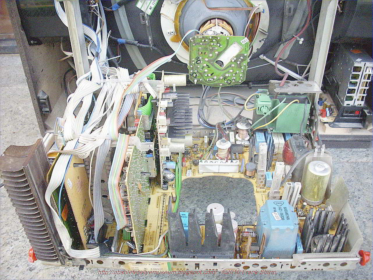 The
invention relates to a blocking oscillator type switching power supply
for supplying power to electrical equipment, wherein the primary
winding of a transformer, in series with the emitter-collector path of a
first bipolar transistor, is connected to a d-c voltage obtained by
rectification of a line a-c voltage fed-in via two external supply
terminals, and a secondary winding of the transformer is provided for
supplying power to the electrical equipment, wherein, furthermore, the
first bipolar transistor has a base controlled by the output of a
control circuit which is acted upon in turn by the rectified a-c line
voltage as actual value and by a set-point transmitter, and wherein a
starting circuit for further control of the base of the first bipolar
transistor is provided.
The
invention relates to a blocking oscillator type switching power supply
for supplying power to electrical equipment, wherein the primary
winding of a transformer, in series with the emitter-collector path of a
first bipolar transistor, is connected to a d-c voltage obtained by
rectification of a line a-c voltage fed-in via two external supply
terminals, and a secondary winding of the transformer is provided for
supplying power to the electrical equipment, wherein, furthermore, the
first bipolar transistor has a base controlled by the output of a
control circuit which is acted upon in turn by the rectified a-c line
voltage as actual value and by a set-point transmitter, and wherein a
starting circuit for further control of the base of the first bipolar
transistor is provided. 
Such a blocking oscillator switching power supply is described in the German periodical, "Funkschau" (1975) No. 5, pages 40 to 44. It is well known that the purpose of such a circuit is to supply electronic equipment, for example, a television set, with stabilized and controlled supply voltages. Essential for such switching power supply is a power switching transistor i.e. a bipolar transistor with high switching speed and high reverse voltage. This transistor therefore constitutes an important component of the control element of the control circuit. Furthermore, a high operating frequency and a transformer intended for a high operating frequency are provided, because generally, a thorough separation of the equipment to be supplied from the supply naturally is desired. Such switching power supplies may be constructed either for synchronized or externally controlled operation or for non-synchronized or free-running operation. A blocking converter is understood to be a switching power supply in which power is delivered to the equipment to be supplied only if the switching transistor establishing the connection between the primary coil of the transformer and the rectified a-c voltage is cut off. The power delivered by the line rectifier to the primary coil of the transformer while the switching transistor is open, is interim-stored in the transformer and then delivered to the consumer on the secondary side of the transformer with the switching transistor cut off.
In the blocking converter described in the aforementioned reference in the literature, "Funkschau" (1975), No. 5, Pages 40 to 44, the power switching transistor is connected in the manner defined in the introduction to this application. In addition, a so-called starting circuit is provided. Because several diodes are generally provided in the overall circuit of a blocking oscillator according to the definition provided in the introduction hereto, it is necessary, in order not to damage these diodes, that due to the collector peak current in the case of a short circuit, no excessive stress of these diodes and possibly existing further sensitive circuit parts can occur.
Considering
the operation of a blocking oscillator, this means that, in the event
of a short circuit, the number of collector current pulses per unit
time must be reduced. For this purpose, a control and regulating
circuit is provided. Simultaneously, a starting circuit must bring the
blocking converter back to normal operation when the equipment is
switched on, and after disturbances, for example, in the event of a
short circuit. The starting circuit shown in the literature reference
"Funkschau" on Page 42 thereof, differs to some extent already from the
conventional d-c starting circuits. It is commonly known for all
heretofore known blocking oscillator circuits, however, that a
thyristor or an equivalent circuit replacing the thyristor is essential
for the operation of the control circuit. 
It is accordingly an object of the invention to provide another starting circuit. It is a further object of the invention to provide a possible circuit for the control circuit which is particularly well suited for this purpose. It is yet another object of the invention to provide such a power supply which is assured of operation over the entire range of line voltages from 90 to 270 V a-c, while the secondary voltages and secondary load variations between no-load and short circuit are largely constant.
With the foregoing and other objects in view, there is provided, in accordance with the invention, a blocking oscillator-type switching power supply for supplying power to electrical equipment wherein a primary winding of a transformer, in series with an emitter-collector path of a first bipolar transistor, is connected to a d-c voltage obtained by rectification of a line a-c voltage fed-in via two external supply terminals, a secondary winding of the transformer being connectible to the electrical equipment for supplying power thereto, the first bipolar transistor having a base controlled by the output of a control circuit acted upon, in turn, by the rectified a-c line voltage as actual value and by a set-point transmitter, and including a starting circuit for further control of the base of the first bipolar transistor, including a first diode in the starting circuit having an anode directly connected to one of the supply terminals supplied by the a-c line voltage and a cathode connected via a resistor to an input serving to supply power to the control circuit, the input being directly connected to a cathode of a second diode, the second diode having an anode connected to one terminal of another secondary winding of the transformer, the other secondary winding having another terminal connected to the emitter of the first bipolar transmitter.
In accordance with another feature of the invention, there is provided a second bipolar transistor having the same conduction type as that of the first bipolar transistor and connected in the starting circuit with the base thereof connected to a cathode of a semiconductor diode, the semiconductor diode having an anode connected to the emitter of the first bipolar transistor, the second bipolar transistor having a collector connected via a resistor to a cathode of the first diode in the starting circuit, and having an emitter connected to the input serving to supply power to the control circuit and also connected to the cathode of the second diode which is connected to the other secondary winding of the transformer.
In accordance with a further feature of the invention, the base of the second bipolar transistor is connected to a resistor and via the latter to one pole of a first capacitor, the anode of the first diode being connected to the other pole of the first capacitor.
In
accordance with an added feature of the invention, the input serving
to supply power to the control circuit is connected via a second
capacitor to an output of a line rectifier, the output of the line
rectifier being directly connected to the emitter of the first bipolar
transistor. In accordance with an additional feature of the invention, the other secondary winding is connected at one end to the emitter of the first bipolar transistor and to a pole of a third capacitor, the third capacitor having another pole connected, on the one hand, via a resistor, to the other end of the other secondary winding and, on the other hand, to a cathode of a third diode, the third diode having an anode connected via a potentiometer to an actual value input of the control circuit and, via a fourth capacitor, to the emitter of the first bipolar transistor.
In accordance with yet another feature of the invention, the control circuit has a control output connected via a fifth capacitor to the base of the first bipolar transistor for conducting to the latter control pulses generated in the control circuit.
In accordance with a concomitant feature of the invention, there is provided a sixth capacitor shunting the emitter-collector path of the first transistor.
Other features which are considered as characteristic for the invention are set forth in the appended claim.
Although the invention is illustrated and described herein as embodied in a blocking oscillator type switching power supply, it is nevertheless not intended to be limited to the details shown, since various modifications and structural changes may be made therein without departing from the spirit of the invention and within the scope and range of equivalents of the claims.
The construction and method of operation of the invention, however, together with additional objects and advantages thereof will be best understood from the following description of specific embodiments when read in connection with the accompanying drawings, in which:
FIGS. 1 and 2 are circuit diagrams of the blocking oscillator type switching power supply according to the invention; and
FIG. 3 is a circuit diagram of the control unit RS of FIGS. 1 and 2.
Referring now to the drawing and, first, particularly to FIG. 1 thereof, there is shown a rectifier circuit G in the form of a bridge current, which is acted upon by a line input represented by two supply terminals 1' and 2'. Rectifier outputs 3' and 4' are shunted by an emitter-collector path of an NPN power transistor T1 i.e. t
 he
series connection of the so-called first bipolar transistor referred to
hereinbefore with a primary winding I of a transformer Tr. Together
with the inductance of the transformer Tr, the capacitance C1 determines
the frequency and limits the opening voltages of the switch embodied by
the first transistor T1. A capacitance C2, provided between the base of
the first transistor T1 and the control output 7,8 of a control circuit
RS, separates the d-c potentials of the control or regulating circuit
RS and the switching transistor T1 and serves for addressing this
switching transistor T1 with pulses. A resistor R1 provided at the
control output 7,8 of the control circuit RS is the negative-feedback
resistor of both output stages of the control circuit RS. It determines
the maximally possible output pulse current of the control circuit RS. A
secondary winding II of the transformer Tr takes over the power supply
of the control circuit, in steady state operation, via the diode D1. To
this end, the cathode of this diode D1 is directly connected to a power
supply input 9 of the control circuit RS, while the anode thereof is
connected to one terminal of the secondary winding II. The other
terminal of the secondary winding II is connected to the emitter of the
power switching transistor T1.
he
series connection of the so-called first bipolar transistor referred to
hereinbefore with a primary winding I of a transformer Tr. Together
with the inductance of the transformer Tr, the capacitance C1 determines
the frequency and limits the opening voltages of the switch embodied by
the first transistor T1. A capacitance C2, provided between the base of
the first transistor T1 and the control output 7,8 of a control circuit
RS, separates the d-c potentials of the control or regulating circuit
RS and the switching transistor T1 and serves for addressing this
switching transistor T1 with pulses. A resistor R1 provided at the
control output 7,8 of the control circuit RS is the negative-feedback
resistor of both output stages of the control circuit RS. It determines
the maximally possible output pulse current of the control circuit RS. A
secondary winding II of the transformer Tr takes over the power supply
of the control circuit, in steady state operation, via the diode D1. To
this end, the cathode of this diode D1 is directly connected to a power
supply input 9 of the control circuit RS, while the anode thereof is
connected to one terminal of the secondary winding II. The other
terminal of the secondary winding II is connected to the emitter of the
power switching transistor T1.The cathode of the diode D1 and, therewith, the power supply terminal 9 of the control circuits RS are furthermore connected to one pole of a capacitor C3, the other pole of which is connected to the output 3' of the rectifier G. The capacitance of this capacitor C3 thereby smoothes the positive half-wave pulses and serves simultaneously as an energy storage device during the starting period. Another secondary windi
ng
III of the transformer Tr is connected by one of the leads thereof
likewise to the emitter of the first transistor T1, and by the other
lead thereof via a resistor R2, to one of the poles of a further
capacitor C4, the other pole of which is connected to the
first-mentioned lead of the other secondary winding III. This second
pole of the capacitor C4 is simultaneously connected to the output 3' of
the rectifier circuit G and, thereby, via the capacitor C3, to the
cathode of the diode D1 driven by the secondary winding II of the
transformer Tr as well as to the power supply input 9 of the control
circuit RS and, via a resistor R9, to the cathode of a second diode D4.
The second pole of the capacitor C4 is simultaneously connected directly
to the terminal 6 of the control circuit RS and, via a further
capacitor C 6, to the terminal 4 of the control circuit RS as well as,
additionally, via the resistor R6, to the other output 4' of the
rectifier circuit G. The other of the poles of the capacitor C4 acted
upon by the secondary winding II is connected via a further capacitor C5
to a node, which is connected on one side thereof, via a variable
resistor R4, to the terminals 1 and 3 of the control circuit RS, with
the intermediary of a fixed resistor R5 in the case of the terminal 1.
On the other side of the node, the latter and, therefore, the capacitor
C5 are connected to the anode of a third diode D2, the cathode of which
is connected on the one hand, to the resistor R2 mentioned hereinbefore
and leads to the secondary winding III of the transformer Tr and, on the
other hand, via a resistor R3 to the terminal 2 of the control circuit
RS.
The nine terminals of the control circuit RS have the following purposes or functions:
Terminal 1 supplies the internally generated reference voltage to ground i.e. the nominal or reference value required for the control or regulating process;
Terminal 2 serves as input for the oscillations provided by the secondary winding III, at the zero point of which, the pulse start of the driving pulse takes place;
Terminal 3 is the control input, at which the existing actual value is communicated to the control circuit RS, that actual value being generated by the rectified oscillations at the secondary winding III;
Terminal 4 is responsive to the occurrence of a maximum excursion i.e. when the largest current flows through the first transistor T1 ;
Terminal 5 is a protective input which responds if the rectified line voltage drops too sharply; Terminal 6 serves for the power supply of the control process and, indeed, as ground terminal;
Terminal 7 supplies the d-c component required for charging the coupling capacitor C2 leading to the base of the first transistor T1 ;
Terminal 8 supplies the control pulse required for the base of the first transistor T1 ; and
Terminal 9 serves as the first terminal of the power supply of the control circuit RS.
Further details of the control circuit RS are described hereinbelow.
The capacity C3 smoothes the positive half-wave pulses which are provided by the secondary winding II, and simultaneously serves as an energy storage device during the starting time. The secondary winding III generates the control voltage and is simultaneously used
 as
feedback. The time delay stage R2 /C4 keeps harmonics and fast
interference spikes away from the control circuit RS. The resistor R3 is
provided as a voltage divider for the second terminal of the control
circuit RS. The diode D2 rectifies the control pulses delivered by the
secondary winding III. The capacity C5 smoothes the control voltage. A
reference voltage Uref, which is referred to ground i.e. the potential
of terminal 6 is present at the terminal 1 of the control circuit RS.
The resistors R4 and R5 form a voltage divider of the input-difference
control amplifier at the terminal 3. The desired secondary voltage can
be set manually via the variable resistor R4. A time-delay stage R6 /C6
forms a sawtooth rise which corresponds to the collector current rise of
the first bipolar transistor T1 via the primary winding I of the
transformer Tr. The sawtooth present at the terminal 4 of the control
circuit RS is limited there between the reference voltage 2 V and 4 V.
The voltage divider R7 /R8 (FIG. 2), brings to the terminal 5 of the
control circuit RS the enabling voltage for the drive pulse at the
output 8 of the control circuit RS.
as
feedback. The time delay stage R2 /C4 keeps harmonics and fast
interference spikes away from the control circuit RS. The resistor R3 is
provided as a voltage divider for the second terminal of the control
circuit RS. The diode D2 rectifies the control pulses delivered by the
secondary winding III. The capacity C5 smoothes the control voltage. A
reference voltage Uref, which is referred to ground i.e. the potential
of terminal 6 is present at the terminal 1 of the control circuit RS.
The resistors R4 and R5 form a voltage divider of the input-difference
control amplifier at the terminal 3. The desired secondary voltage can
be set manually via the variable resistor R4. A time-delay stage R6 /C6
forms a sawtooth rise which corresponds to the collector current rise of
the first bipolar transistor T1 via the primary winding I of the
transformer Tr. The sawtooth present at the terminal 4 of the control
circuit RS is limited there between the reference voltage 2 V and 4 V.
The voltage divider R7 /R8 (FIG. 2), brings to the terminal 5 of the
control circuit RS the enabling voltage for the drive pulse at the
output 8 of the control circuit RS.The diode D4, together with the resistor R9 in cooperation with the diode D1 and the secondary winding II, forms the starting circuit provided, in accordance with the invention. The operation thereof is as follows:
After the switching power supply is switched on, d-c voltages build up at the collector of the switching transistor T1 and at the input 4 of the control circuit RS, as a function in time of the predetermined time constants. The positive sinusoidal half-waves charge the capacitor C3 via the starting diode D4 and the starting resistor R9 in dependence upon the time constant R9.C3. Via the protective input terminal 5 and the resisto
r
R11 not previously mentioned and forming the connection between the
resistor R9 and the diode D1, on the one hand, and the terminal 5 of the
control circuit RS, on the other hand, the control circuit RS is biased
ready for switching-on, and the capacitor C2 is charged via the output
7. When a predetermined voltage value at the capacitor C3 or the power
supply input 9 of the control circuit RS, respectively, is reached, the
reference voltage i.e. the nominal value for the operation of the
control voltage RS, is abruptly formed, which supplies all stages of the
control circuit and appears at the output 1 thereof. Simultaneously,
the switching transistor T1 is switched into conduction via the output
8. The switching of the transistor T1 at the primary winding T of the
transformer Tr is transformed to the second secondary winding II, the
capacity C3 being thereby charged up again via the diode D1. If
sufficient energy is stored in the capacitor C3 and if the re-charge via
the diode D1 is sufficient so that the voltage at a supply input 9 does
not fall below the given minimum operating voltage, the switching power
supply then remains connected, so that the starting process is
completed. Otherwise, the starting process described is repeated several
times.In FIG. 2, there is shown a further embodiment of the circuit for a blocking oscillator type switching power supply, according to the invention, as shown in FIG. 1. Essential for this circuit of FIG. 2 is the presence of a second bipolar transistor T2 of the type of the first bipolar transistor T1 (i.e. in the embodiments of the invention, an npn-transistor), which forms a further component of the starting circuit and is connected with the collector-emitter path thereof between the resistor R9 of the starting circuit and the current supply input 9 of the control circuit RS. The base of this second transistor T2 is connected to a node which leads, on the one hand, via a resistor R10 to one electrode of a capacitor C7, the other electrode of which is connected to the anode of the diode D4 of the starting circuit and, accordingl
 y,
to the terminal 1' of the supply input of the switching power supply G.
On the other hand, the last-mentioned node and, therefore, the base of
the second transistor T2 are connected to the cathode of a Zener diode
D3, the anode of which is connected to the output 3' of the rectifier G
and, whereby, to one pole of the capacitor C3, the second pole of which
is connected to the power supply input 9 of the control circuit RS as
well as to the cathode of the diode D1 and to the emitter of the second
transistor T2. In other respects, the circuit according to FIG. 2
corresponds to the circuit according to FIG. 1 except for the resistor
R11 which is not necessary in the embodiment of FIG. 2, and the missing
connection between the resistor R9 and the cathode of the diode D1,
respectively, and the protective input 5 of the control circuit RS.
y,
to the terminal 1' of the supply input of the switching power supply G.
On the other hand, the last-mentioned node and, therefore, the base of
the second transistor T2 are connected to the cathode of a Zener diode
D3, the anode of which is connected to the output 3' of the rectifier G
and, whereby, to one pole of the capacitor C3, the second pole of which
is connected to the power supply input 9 of the control circuit RS as
well as to the cathode of the diode D1 and to the emitter of the second
transistor T2. In other respects, the circuit according to FIG. 2
corresponds to the circuit according to FIG. 1 except for the resistor
R11 which is not necessary in the embodiment of FIG. 2, and the missing
connection between the resistor R9 and the cathode of the diode D1,
respectively, and the protective input 5 of the control circuit RS.Regarding the operation of the starting circuit according to FIG. 2,
 it can be stated that the positive sinusoidal half-wave of the line
voltage, delayed by the time delay stage C7, R10 drives the base of the
transistor T2 in the starting circuit. The amplitude is limited by the
diode D3 which is provided for overvoltage protection of the control
circuit RS and which is preferably incorporated as a Zener diode. The
second transistor T2 is switched into conduction. The capacity C3 is
charged, via the serially connected diode D4 and the resistor R9 and the
collector-emitter path of the transistor T2, as soon as the voltage
between the terminal 9 and the terminal 6 of the control circuit RS i.e.
the voltage U9, meets the condition U9 <[UDs -UBE (T2)].
it can be stated that the positive sinusoidal half-wave of the line
voltage, delayed by the time delay stage C7, R10 drives the base of the
transistor T2 in the starting circuit. The amplitude is limited by the
diode D3 which is provided for overvoltage protection of the control
circuit RS and which is preferably incorporated as a Zener diode. The
second transistor T2 is switched into conduction. The capacity C3 is
charged, via the serially connected diode D4 and the resistor R9 and the
collector-emitter path of the transistor T2, as soon as the voltage
between the terminal 9 and the terminal 6 of the control circuit RS i.e.
the voltage U9, meets the condition U9 <[UDs -UBE (T2)].Because of the time constant R9.C3, several positive half-waves are necessary in order to increase the voltage U9 at the supply terminal 9 of the control circuit RS to such an extent that the control circuit RS is energized. During the negative sine half-wave, a partial energy chargeback takes place from the capacitor C3 via the emitter-base path of the transistor T2 of the starting circuit and via the resistor R10 and the capacitor C7, respectively, into the supply network. At approximately 2/3 of the voltage U9, which is limited by the diode D3, the control circuit RS is switched on. At the terminal 1 thereof, the reference voltage Uref then appears. In addition, the voltage divider R5 /R4 becomes effective. At the terminal 3, the control amplifier receives the voltage forming the actual value, while the first bipolar transistor T1 of the blocking-oscillator type switching power supply is addressed pulsewise via the terminal 8.
Because the capacitor C6 is charged via the resistor R6, a higher voltage than Uref is present at the terminal 4 if the control circuit RS is activated. The control voltage then discharges the capacitor C6 via the terminal 4 to half the value of the reference voltage Uref, and immediately cuts off the addressing input 8 of the control circuit RS. The first driving pulse of the switching transistor T1 is thereby limited to a minimum of time. The power for switching-on the control circuit RS and for driving the transistor T1 is supplied by the capacitor C3. The voltage U9 at the capacitor C3 then drops. If the voltage U9 drops below the switching-off voltage value of the control circuit RS, the latter is then inactivated. The next positive sine half-wave would initiate the starting process again.
By switching the transistor T1, a voltage is transformed in the secondary winding II of the transformer Tr. The positive component is rectified by the diode D1, recharing of the capacitor C3 being thereby provided. The voltage U9 at the output 9 does not, therefore, drop below the minimum value required for the operation of the control circuit RS, so that the control circuit RS remains activated. The power supply continues to operate in the rhythm of the existing conditions. In operation, the voltage U9 at the supply terminal 9 of the control circuit RS has a value which meets the condition U9 >[UDs -UBE (T2)], so that the transistor T2 of the starting circuit remains cut off.
For the internal layout of the control circuit RS, the construction shown, in particular, from FIG. 3 is advisable. This construction is realized, for example, in the commercially available type TDA 4600 (Siemens AG).
The block diagram of the control circuit according to FIG. 3
 shows
the power supply thereof via the terminal 9, the output stage being
supplied directly whereas all other stages are supplied via Uref. In the
starting circuit, the individual subassemblies are supplied with power
sequentially. The d-c output voltage potential of the base current gain
i.e. the voltage for the terminal 8 of the control circuit RS, and the
charging of the capacitor C2 via the terminal 7 are formed even before
the reference voltage Uref appears. Variations of the supply voltage U9
at terminal 9 and the power fluctuations at the terminal 8/terminal 7
and at the terminal 1 of the control circuit RS are leveled or smoothed
out by the voltage control. The temperature sensitivity of the control
circuit RS and, in particular, the uneven heating of the output and
input stages and input stages on the semiconductor chip containing the
control circuit in monolithically integrated form are intercepted by the
temperature compensation provided. The output values are constant in a
specific temperature range. The message for blocking the output stage,
if the supply voltage at the terminal 9 is too low, is given also by
this subassembly to a provided control logic.
shows
the power supply thereof via the terminal 9, the output stage being
supplied directly whereas all other stages are supplied via Uref. In the
starting circuit, the individual subassemblies are supplied with power
sequentially. The d-c output voltage potential of the base current gain
i.e. the voltage for the terminal 8 of the control circuit RS, and the
charging of the capacitor C2 via the terminal 7 are formed even before
the reference voltage Uref appears. Variations of the supply voltage U9
at terminal 9 and the power fluctuations at the terminal 8/terminal 7
and at the terminal 1 of the control circuit RS are leveled or smoothed
out by the voltage control. The temperature sensitivity of the control
circuit RS and, in particular, the uneven heating of the output and
input stages and input stages on the semiconductor chip containing the
control circuit in monolithically integrated form are intercepted by the
temperature compensation provided. The output values are constant in a
specific temperature range. The message for blocking the output stage,
if the supply voltage at the terminal 9 is too low, is given also by
this subassembly to a provided control logic.The outer voltage divider of the terminal 1 via the r
esistors
R5 and R4 to the control tap U forms, via terminal 3, the variable side
of the bridge for the control amplifier formed as a differential
amplifier. The fixed bridge side is formed by the reference voltage Uref
via an internal voltage divider. Similarly formed are circuit portions
serving for the detection of an overload short circuit and circuit
portions serving for the "standby" no-load detection, which can be
operated likewise via terminal 3.Within a provided trigger circuit, the driving pulse length is determined as a function of the sawtooth rise at the terminal 4, and is transmitted to the control logic. In the control logic, the commands of the trigger circuit are processed. Through the zero-crossing identification at input 2 in the control circuit RS, the control logic is enabled to start the control input only at the zero point of the frequency oscillation. If the voltages at the terminal 5 and at the terminal 9 are too low, the control logic blocks the output amplifier at the terminal 8. The output amplifier at the terminal 7 which is responsible for the base charge in the capacitor C2, is not touched thereby.
The base current gain for the transistor T1 i.e. for the first transistor in accordance with the definition of the invention, is formed by two amplifiers which mutually operate on the capacitor C2. The roof inclination of the base driving current for the transistor T1 is impressed by the collector current simulation at the terminal 4 to the amplifier at the terminal 8. The control pulse for the transistor T1 at the terminal 8 is always built up to the potential present at the terminal 7. The amplifier working into the terminal 7 ensures that each new switching pulse at the terminal 8 finds the required base level at terminal 7.
Supplementing the comments regarding FIG. 1, it should also be mentioned that the cathode of the diode D1 connected by the anode thereof to the one end of the secondary winding II of the transformer Tr is connected via a resistor R11 to the protective input 5 of the control circuit RS whereas, in the circuit according to FIG. 2, the protective input 5 of the control circuit RS is supplied via a voltage divider R8, R7 directly from the output 3', 4' of the rectifier G delivering the rectified line a-c voltage, and which obtains the voltage required for executing its function. It is evident that the first possible manner of driving the protective input 5 can be used also in the circuit according to FIG. 2, and the second possibility also in a circuit in accordance with FIG. 1.
The control circuit RS which is shown in FIG. 3 and is realized in detail by the building block TDA 4600 and which is particularly well suited in conjunction with the blocking oscillator type switching power supply according to the invention has 9 terminals 1-9, which have the following characteristics, as has been explained in essence hereinabove:
Terminal 1 delivers a reference voltage Uref which serves as the constant-current source of a voltage divider R5.R4 which supplies the required d-c voltages for the differential amplifiers provided for the functions control, overload detection, short-circuit detection and "standby"-no load detection. The dividing point of the voltage divider R5 -R4 is connected to the terminal 3 of the control circuit RS. The terminal 3 provided as the control input of RS is controlled in the manner described hereinabove as input for the actual value of the voltage to be controlled or regulated by the secondary winding III of the transformer Tr. With this input, the lengths of the control pulses for the switching transistor T1 are determined.
Via the input provided by the terminal 2 of the control circuit RS, the zero-point identification in the control circuit is addressed for detecting the zero-point o
f
the oscillations respectively applied to the terminal 2. If this
oscillation changes over to the positive part, then the addressing pulse
controlling the switching transistor T1 via the terminal 8 is released
in the control logic provided in the control circuit.A sawtooth-shaped voltage, the rise of which corresponds to the collector current of the switching transistor T1, is present at the terminal 4 and is minimally and maximally limited by two reference voltages. The sawtooth voltage serves, on the one hand as a comparator for the pulse length while, on the other hand, the slope or rise thereof is used to obtain in the base current amplification for the switching transistor T1, via the terminal 8, a base drive of this switching transistor T1 which is proportional to the collector current.
The terminal 7 of the control circuit RS as explained hereinbefore, determines the voltage potential for the addressing pulses of the transistor T2. The base of the switching transistor T1 is pulse-controlled via the terminal 8, as described hereinbefore. Terminal 9 is connected as the power supply input of the control circuit RS. If a voltage level falls below a given value, the terminal 8 is blocked. If a given positive value of the voltage level is exceeded, the control circuit is activated. The terminal 5 releases the terminal 8 only if a given voltage potential is present.
Forei
 gn References:
DE2417628A1 1975-10-23 363/37
DE2638225A1 1978-03-02 363/49
Other References:
Grundig Tech. Info. (Germany), vol. 28, No. 4, (1981).
IBM Technical Disclosure Bulletin, vol. 19, No. 3, pp. 978, 979, Aug. 1976.
German Periodical, "Funkschau", (1975), No. 5, pp. 40 to 44.
Siemens Aktiengesellschaft (Berlin and Munich, DE)
TDA8170 TV VERTICAL DEFLECTION OUTPUT CIRCUIT:DESCRIPTION
The TDA8170 is a monolithic integrated circuit in
HEPTAWATT packa
ge. It is a high efficiency
power booster for direct driving of verticalwindings
of TV yokes. It is intended for use in Colour and B
&Wtelevision receivers as well as in monitorsand
displays.
The functions incorporated are :
.POWERAMPLIFIER
.FLYBACKGENERATOR
.REFERENCE VOLTAGE
.THERMAL PROTECTION
The power dissipated in the circuit must be removed
by adding an external heatsink.
Thanks to the HEPTAWATTTM package attaching
the heatsink is very simple, a screwa compression
spring (clip) being sufficient. Betweenthe heatsink
andthe packageit isbetter to insert a layerof silicon
grease, to optimizethe thermal contact ; no electrical
isolation is needed between the two surfaces.
Typically, a vertical deflection circuit of, for example, a television
receiver includes an amplifier referred to as the vertical amplifier
having a push-pull output stage. An output terminal of the push-pull
output stage is coupled to a series arrangement of a vertical deflection
winding, a DC blocking capacitor and a deflection current sampling
resistor for producing a vertical deflection current in the series
arrangement. A sawtooth feedback voltage developed in the sampling
resistor and a sawtooth input voltage are coupled to an input of the
amplifier to form a closed loop feedback operation mode, during vertical
trace.
During vertical retrace, one of the transistors of the
push-pull output stage operates as a switch to couple a boosted-up
supply voltage to the deflection winding that causes the deflection
current to reverse its polarity. After the deflection current reverses
its polarity and attains approximately a peak value, that transistor
begins operating as an amplifier stage and the vertical amplifier
operates again in the closed loop feedback operation mode. Thus,
vertical trace is resumed.
ABSOLUTE MAXIMUM RATINGS
Symbol Parameter Value Unit
VS Supply Voltage (pin 2) 35 V
V5, V6 Flyback Peak Voltage 60 V
V3 Voltage at Pin 3 + Vs
V1, V7 Amplifier Input Voltage + Vs, – 0.5 V
Io Output Peak Current (non repetitive, t = 2 msec) 2.5 A
Io Output Peak Current at f = 50 or 60 Hz, t 3 10 msec 3 A
Io Output Peak Current at f = 50 or 60 Hz, t > 10 msec 2 A
I3 Pin 3 DC Current at V5 < V2 100 mA
I3 Pin 3 Peak to Peak Flyback Current at f= 50 or 60 Hz, tfly 31.5msec 3 A
Ptot Total Power Dissipation at Tcase = 90 °C 20 W
Tstg, Tj Storage and Junction Temperature – 40, +150 °C
TDA2009 AUDIO IC AMPLIFIER:10 +10W STEREO AMPLIFIER,DESCRIPTION
The TDA2009Ais class AB dual Hi-Fi Audio power
amplifier assembled in Multiwatt [ package, specially
designed for high quality stereo application
as Hi-Fi and music centers.
.HIGH OUTPUT POWER
(10 + 10W Min.@D = 1%)
.HIGH CURRENT CAPABILITY (UP TO 3.5A)
.AC SHORT CIRCUIT PROTECTION
.THERMAL OVERLOADPROTECTION
.SPACE AND COST SAVING : VERY LOW
NUMBER OF EXTERNAL COMPONENTS
AND SIMPLE MOUNTING THANKS TO THE
MULTIWATT [ PACKAGE.
BS843.1 (60.3022.103) TELETEXT UNIT(PHILIPS SAA5231
PHILIPS SAA5243 -0.3 to +7.5V enhanced computer controlled teletext circuits (ECCT)
PHILIPS FCB61C65L-70P)
SAA5231 Teletext video processor
GENERAL DESCRIPTION
The SAA5231 is a bipolar integrated circuit intended as a successor to the SAA5030. It extracts Teletext Data from the
video signal, regenerates Teletext Clock and synchronizes the text display to the television syncs. The integrated circuit
is intended to work in conjunction with CCT (Computer Controlled Teletext), EUROM or other compatible devices.
Features:
• Adaptive data slicer
• Data clock regenerator
• Adaptive sync separator, horizontal phase detector and 6 MHz VCO forming display phase locked loop (PLL)
The function is quoted against the corresponding pin number.
1. Synch output to TV
Output with dual polarity buffer, a load resistor to 0 V or + 12 V selects positive-going or negative-going syncs.
2. Video input level select
When this pin is LOW a 1 V video input level is selected. When the pin is not connected it floats HIGH selecting a
2,5 V video input level.
3. HF filter
The video signal for the h.f.-loss compensator is filtered by a 15 pF capacitor connected to this pin.
4. Store h.f.
The h.f. amplitude is stored by a 1 nF capacitor connected to this pin.
5. Store amplitude
The amplitude for the adaptive data slicer is stored by a 470 pF capacitor connected to this pin.
6. Store zero level
The zero level for the adaptive data slicer is stored by a 22 nF capacitor connected to this pin.
7. External data input
Current input for sliced teletext data from external device.
Active HIGH level (current), low impedance input.
8. Data timing
A 270 pF capacitor is connected to this pin for timing of the adaptive data slicer.
9. Store phase
The output signal from the clock phase detector is stored by a 100 pF capacitor connected to this pin.
10. Video tape recorder mode (VCR)
Signal input to command PLL into short time constant mode. Not used in application circuit Fig.4a or Fig.4b.
11. Crystal
A 13,875 MHz crystal, 2 x data rate, connected in series with a 15 pF capacitor is applied via this pin to the oscillator
and divide-by-two to provide the 6,9375 MHz clock signal.
12. Clock filter
A filter for the 6,9375 MHz clock signal is connected to this pin.
13. Ground (0 V)
14. Teletext clock output (TTC)
Clock output for CCT (Computer Controlled Teletext).
15. Teletext data output (TTD)
Data output for CCT.
16. Supply voltage VCC (+ 12 V typ.)
17. Clock output (F6)
6 MHz clock output for timing and sandcastle generation in CCT.
18. Oscillator output (6 MHz)
A series resonant circuit is connected between this pin and pin 20 to control the nominal frequency of the VCO.
19. Filter 2
A filter with a short time constant is connected to this pin for the horizontal phase detector. It is used in the video
recorder mode and while the loop is locking up.
20. Oscillator input (6 MHz)
See pin 18.
21. Filter 1
A filter with a long time constant is connected to this pin for the horizontal phase detector.
22. Sandcastle input pulse (PL/CBB)
This input accepts a sandcastle waveform, which is formed from PL and CBB from the CCT.
Signal timing is shown in Fig.5.
23. Pulse timing resistor
The current for the pulse generator is defined by a 68 Ω resistor connected to this pin.
24. Pulse timing capacitor
The timing of the pulse generator is determined by a 220 pF capacitor connected to this pin.
25. Video composite sync output (VCS)
The output signal is for CCT.
26. Black level
The black level for the adaptive sync separator is stored by a 68 nF capacitor connected to this pin.
27. Composite video input (CVS)
The composite video signal is input via a 2,2 μF clamping capacitor to the adaptive sync separator.
28. Text composite sync input (TCS)/Scan composite sync input (SCS)
TCS is input from CCT or SCS from external sync circuit. SCS is expected when there is no load resistor at pin 1.
If pin 28 is not connected the sync output on pin 1 will be the composite video input at pin 27, internally buffered.
PHILIPS TDA4502A SMALL SIGNAL COMBINATION FOR COLOUR TV
GENERAL DESCRIPTION
The integration into a single package of all small signal functions required for colour TV reception is
achieved in the TDA4502A. The only additional circuits required for colour TV reception are the
deflection output stages, a sound detector and amplifier, and a colour decoder.
The IC includes a vision IF amplifier and video switching circuit, AFC circuit, AGC detector with
tuner output, an integral three—level sandcastle pulse generator, fully synchronized vertical and
horizontal drive outputs and a mute circuit with external availability. A triggered vertical divider
automatically adapts to 50 or 60 Hz operating mode thereby eliminating the need for external vertical
frequency control. The sound signal must be demodulated and amplified externally.
Features
Vision IF amplifier with synchronous demodulator
AGC detector, suitable for negative modulation
AGC output to tuner
AFC circuit with ON/OFF switch

Video preamplifier
Video switch to select the internal, or an external, video signal
Horizontal synchronization circuit with two control loops
Vertical synchronization [divider system) and sawtooth generation with automatic amplitude
adjustment for 50 and 60 Hz
Transmitter identification (mute)
O Sandcastle pulse generator
QUICK REFERENCE DATA
K7 parameter symbol min. typ. max. unitSupply voltage (pin 7) V7 9.5 12 13.2 V
Supply current (pin 7) I7 — 125 — ‘ mA
Supply current (pin 11) ‘‘ V11 — 6.0 8.5 mA
Operating ambient temperature range Tamb -25 - + 65 °C
Storage temperature range Tstg -25 — + 150 °C
Total power dissipation Ptot — — 2.3 W
PACKAGE OUTLINE
28—lead DI L; plastic with internal heat spreader (SOT117).
TDA4502A
FUNCTIONAL DESCRIPTION
IF amplifier, synchronous demodulator and AFC
The IF amplifier (pins 8 and 9) has a symmetrical input, the impedance of which enables SAW-filtering
to be used. The synchronous demodulator and the AFC circuit share an external reference tuned
circuit (pins 20 and 21). An internal RC—network provides the necessary phase—shift for AFC operation.
The AFC circuit provides a control voltage output with a voltage swing greater than 9 V at pin 18.
In the internal and external mode the AFC can be switched OFF when pin 22 is connected to positive
supply.
AGC circuit
AGC gating is performed to reduce sensitivity of the IF amplifier to external noise. The AGC timeconstant is provided by an RC circuit 19.
agc connected from is pin supplied tuner voltage pin 5. The point of tuner takeover is preset by the voltage level at pin 1.
Video switch circuit
The IC has a video switch with two video inputs and one video output. One input is connected to the
demodulated IF signal which is also fed to the video output pin of the peritelevision connector. The
other input can be switched to an external signal which is applied to the video input of the
peritelevision connector. The video output signal of the switch is fed to pin 25 of the IC, which is
the wnchronization part and, to the colour decoder. When the video switch is in the external mode,
the synchronization circuit is switched to the external signal. The vision IF, AGC and AFC circuits
will not be affected by the switching action and will, therefore, operate in the normal mode. Gating
for the AGC detector is switched OFF when the switch is in the external mode. The first control
loop is not switched to a low time constant when weak signals are received.
Horizontal oscillator start function
The horizontal oscillator start function is achieved by applying a current of 8.5 mA to pin 11 during the
switch-on period. This current can be taken from the mains rectifier. The main supply, pin 7, can then
be obtained from the horizontal output stage. The load current of the driver has to be added to the
start current.
Horizontal synchronization
The positive video input signal is applied to pin 25. The horizontal synchronization has two control
loops which have been introduced to generate a sandcastle pulse. By using the oscillator sawtooth, an
accurate timing of the burst-key pulse can be made. Therefore, the phase of this sawtooth pulse must
have a fixed relationship to the sync pulse.
Horizontal phase detector
The circuit has two operating conditions:
(a) Synchronized
The first loop has afixed time constant and a gated phase detector, this enables optimum
performance for co-channel interference. The VCR mode is obtained by an additional load on
pin 22.
(b) Non-synchronized
In this condition the time constant is the same as during the VCR mode.
Vertical sync pulse
The vertical sync pulse integrator will not be disturbed when the vertical sync pulses have a width of
10 ps and a separation of 22 us. This type of vertical sync pulse is generated by video tapes with
anti-copy guard.
Vertical divider system
A synchronized divider system generates the vertical sawtooth wavefonns at pin 2. The system uses an
internal frequency doubler circuit to enable the horizontal oscillator to operate at its normal line
frequency. One line period equals 2 clock pulses.
Using the divider system avoids the requirement for vertical frequency adjustment. The divider has a
discriminator window for automatic switching from 50 Hz to 60 Hz mode. When the trigger pulse
arrives before line 576 the 60 Hz mode is selected, if not, the 50 Hz mode is selected.
The divider system operates with two different reset windows to give maximum interferencel
disturbance protection. The windows are activated via an up/down counter.
The counter is increased by 1 each time the separated vertical sync pulse is within the narrow window.
When the sync pulse is not within the narrow window the counter is decreased by 1.
The operation modes of the divider system are as follows:
Mode A
Large (search) window (divider ratio between 488 and 722)
This mode is valid for the following conditions:
0 Divider is looking for a new transmitter
O Divider ratio found — not within the narrow window limits
0 A non—standard composite video signal is detected — when a double or enlarged vertical sync pulse is
detected after the internally generated anti-top~flutter pulse has ended. This means a vertical sync
pulse width > 10 clock pulses (50 Hz); > 12 clock pulses (60 Hz). This mode is normally activated
for video tape recorders operating in the feature trick mode
0 Up/down counter value of the divider system, operating in the narrow window mode, drops below
count 6
Mode B
Narrow window (divider ratio between 522 to 528 (60 Hz) or 622 to 628 (50 Hz))
The divider system switches over to this mode when the up/down counter has reached its maximum
value of 15 approved vertical sync pulses. When the divider operates in this mode and, a vertical sync
pulse is missing within the window, the divider is reset at the end of the window and the counter value
is decreased by 1. At a counter value below 6 the divider system switches over to the large window
mode.
The divider system also generates an anti—top-flutter pulse which inhibits the Phase 1 detector during
the vertical sync pulse. The pulse width is dependent on the divider mode. In ‘Mode A’ the start is
generated by resetting the divider. In ’Mode B’ the anti—top-flutter pulse starts at the beginning of the
first equalizing pulse. The anti—top-flutter pulse ends at count 10 for the 50 Hz mode and count 12 for
the 60 Hz mode.
The vertical blanking pulse is also generated via the divider system. The start is initiated by resetting
the divider while the blanking pulse width is at count 34, (17 l
ines), for the 60 Hz mode and at
count 42, (21 lines), for the 50 Hz mode. The vertical blanking pulse, at the sandcastle output
(pin 27), is generated by adding the anti—top-flutter pulse to the blanking pulse. When the divider
operates in ‘Mode B’, the vertical blanking pulse starts at the beginning of the first equalizing pulse.
The length of the vertical blanking in this condition is 21 lines in the 60 Hz mode and 25 lines in the
50 Hz mode.
RATINGS
Limiting values in accordance with the Absolute Maximum System llEC 134)
parameter symbol min. max. unit
Supply voltage Vp = V7.5 — 13.2 V
Total power dissipation Pmt - 2.3 W
Operating ambient temperature range Tamb -25 + 65 °C
Storage temperature range Tstg -25 + 150 °C
CHARACTERISTICS
Vp = V7 = 12 V; Tamb = 25 °C; unless otherwise specified; all voltages are referenced to ground
(pin 6) unless otherwise specified
parameter conditions symbol min. typ. max. unit
Supplies
Supply voltage (pin 7) V7 9.5 12.0 13.2 V
Supply current (pin 7) I7 — 125 — mA
Supply current (pin 1 1) note 1 l 11 — 6 8.5 mA
Vision IF amplifier (pins 8 and 9)
Input sensitivity at 38.9 MHz note 2 V8 40 80 120 uV
Input sensitivity at 45.75 MHz note 2 V3 — 100 ~ uV
Differential input resistance
(pin 8 to pin 9) note 3 R3_g 0.8 1.3 1.8 kfl
Differential input capacitance
(pin 8 to pin 9) note 3 C39 — 5 —- pF
Gain control range G3_g — 62 — dB
Maximum input signal V3.9 50 100 — mV
Expansion of output signal for
50 dB variation of input signal note 4 AV17 — 1 — dB
Video amplifier note 5
Output level for zero signal input note 6 V17 3.3 3.7 4.1 V
Output signal top sync level V17 1.5 1.7 1.9 V
Amplitude of video output signal
(peak-to-peak value) note 7 V17(p_p) 1.4 1.8 2.2 V
Internal bias current of output
transistor (npn emitter
follower) l17(int) 1.4 2.0 — mA
Bandwidth of demodulated
output signal B 4.0 5.0 — M Hz
Differential gain note 8 G 17 — 5 10 %
Differential phase note 8 lp — 5 10 %
ITT TVPO2066 TV Controller with On-Screen Display for TV Receivers.
Introduction
In comparison to the older TVPO 2065 hardware, theport 3 of the TVPO 2066 consists of 6 x 12 V/2 mA open–
drain outputs instead of 5 V/25 mA open–drain outputs.
“TVPO 2066” is the name of the unprogrammed hard-
ware. The programmed versions will be called:
– TVPO 2066–Axx
for analog TV–sets
– TVPO 2066–Dxx
for digital TV–sets
with the version–no. xx. Application diagrams and de-
scriptions of different software versions are available in
additional data sheets.
The TVPO 2066 is an intelligent microcomputer in N–
channel MOS technology. On one silicon chip, it con-
tains all operating and tuning functions of a modern TV
receiver. Thus, along with the non–volatile memory
(MDA 2062, NVM 3060), the SAA 1250, IRT 1250 or IRT
1260 remote–control transmitter and the TBA 2800 pre-
amplifier this offers a very economic solution for TV re-
ceivers with on–screen display and voltage synthesizer.
The device is available in 44–pin PLCC package and
40–pin DIL package. The PLCC version has 4 pins more
for digital combined inputs/outputs.
2. The Functional Blocks of the TVPO 2066
The hardware components of the TVPO 2066 are:
– 8048–core, fully compatible to 8048 instruction set
– 10K ROM, 256 byte RAM
– four 64 steps analog output to control vol., color etc.
– single 4032 steps analog output for controlling of a
VS–tuner
– IR decoder for ITT–IR (remote control with IRT
1250/60)
– mains flip–flop for standby mode
– IM–bus interface for non–volatile memory and devices
of DIGIT 2000 system for digital video–processing.
– fast counter input (T1) for automatic search (for analog
TV–sets)
– 12 digital combined inputs/outputs (8 or 10 for DIL–
package)
– 8 digital outputs
– integrated 12–digit on–screen display
2.1. The 8049 Microcomputer
For the description of the commands and characteristics
of the 8049, please refer to the CCU 2030, CCU 2050,
CCU 2070 data sheet.
The 8049 provides separate address space for program,
data, in/out, and external data. The ROM is organized in
banks of 2 K Bytes. Bank 0 occupies the addresses 0 to
2047. The other banks (10, 11, 12, 13) share the ad-
dresses 2048 to 4095. The different banks are selected
through the bank select register 15 as described for the
CCU 2070 in the CCU 2030, 2050, 2070 data sheet.
Banks 14 through 17 of the CCU 2070 are not available
in the TVPO.
The data and control registers of the TVPO’s peripheral
units are located in the address space of external data.
They are accessed by the “Move External” instruction
(MOVX). Electrically, the connection is provided by the
lines DB0 to DB7, RD, WR, and ALE. These connections
of the 8049 microcomputer are not available during nor-
mal operation. In “Test Mode” (EA = 5 V or EA = 12 V),
some pins are switched so that the TVPO’s peripherals
can be accessed from the outside via DB0 to DB7.
In normal operation, only P2 of the 8049’s original ports
remains unchanged. During test operation, RD, WR,
ALE and PSEN are connected to P24 to P27 (compare
CCU 2030, CCU 2050, CCU 2070 data sheet).
2.2. The Remote–Control Decoder
In the already mentioned standby mode, and also during
normal operation, the remote–control decoder expects
infrared–transmitted signals that were transmitted by
the SAA 1250, IRT 1250 or IRT 1260 remote–control
transmitter IC, received by an infrared photo diode, and
amplified by the TBA 2800 infrared preamplifier IC. The
decoder frees the remote–control signal from interfer-
ence and decodes each command word that is recog-
nized as correct. A valid command word is made avail-
able to the microcomputer by way of two registers. No
interrupt is initiated. Rather, it is the task of the program
to continuously check the infrared registers.
A command word transmitted via infrared consists of 10
bits – four address bits and six data bits. These two parts
of the command word are provided in two different regis-
ters. Bit 7 in the address register is low when a valid com-
mand word is detected. When the data word is read,
both infrared registers are cleared.
It is possible to mask–program which infrared com-
mands also carry the power–on information and switch
the TVPO from standby to full operation. For this pur-
pose, up to five groups of commands within a binary de-
coder matrix are programmable for one infrared address
(compare CCU 2030, CCU 2050, CCU 2070 data
sheet).
2.3. The Mains Flip–Flop and Reset Circuit
Mains flip–flop and reset circuit operate from the stand-
by supply. After switching on the standby supply it takes
100 ms at most until the TVPO is in full standby opera-
tion. The Mains output is controlled by the mains flip–
flop. In the
“Mains off” position the output is high.
The mains flip–flop is set by means of the infrared
“Mains on” commands or by an active low level applied
to the Mains output for at least 20 µs. A reset for the
mains flip–flop is generated whenever:
1. The standby supply voltage is less than approx. 3.5 V
(e.g. during power–on)
2. The microcomputer executes a “Mains off” command.
The microcomputer clears the mains flip–flop by writing
a 1 into bit 3 of the external register 13. In order to proper-
ly charge the stray capacitances at the Mains output, the
mains flip–flop remains blocked in the “Mains off” posi-
tion for 16 ms after any reset. After this time has elapsed,
the TV set may be turned on again.
With no Reset option set (compare CCU 2030, CCU
2050, CCU 2070 data sheet), the mains flip–flop is also
reset by any Reset signal going low. The TVPO–internal
Reset’, which is different from the externally–applied
Reset is high only when both Mains is in the low state
and Reset is at high level. Two options are mask–pro-
grammable in this respect:
Reset 1: The Reset signal, going low, does not reset the
mains flip–flop. If the customer does not specify, this op-
tion will be set as default.
Reset 2: The TVPO–internal Reset’ is identical to the
Reset signal and independent of the state of the mains
flip–flop.
Resetting the mains flip–flop clears the remote–control
decoder. The other parts of the TVPO are cleared by the
TVPO–internal Reset’ signal via the Reset input. Delay-
ing the Reset signal with respect to the VDD supply volt-
age is done by an external RC network at the Reset in-
put.
The input voltage of the regulator for the 5 V VDD supply
voltage should be monitored to prevent the system’s cir-
cuits from resetting improperly and the NVM 3060 EE-
PROM from programming false data.
With no Reset option set, any spike or excessive noise
present on the Reset line may cause the mains flip–flop
to be reset. In such cases, a ceramic filter capacitor
should be provided near the Reset pin.
2.4. The IM–Bus and Non–Volatile–Memory
It is by means of this part of the circuit that the TVPO
2066 communicates with the non–volatile memory
(MDA 2062 or NVM 3060) which stores the tuning and
analog data, acquired during the Memo procedure and
the options. The IM–Bus consists of three lines Clock,
Ident and Data. Clock and Ident are unidirectional sig-
nals from the TVPO 2066 to the memory (and to the
VSP–processor in case of a digital TV set), and Data is
bidirectional for transferring the data in both directions.
In addition, the MDA 2062 (not the NVM 3060) requires
a memory clock signal which is issued from the TVPO
2066 (approx. 1 kHz). All these signals on the IM–Bus
have TTL level. In the nonoperative state all three bus
lines are high. The start of a telegram is initiated when
Ident and Data are low. Data takeover occurs at the posi-
tive edge of Clock. For a detailed description of the IM–
Bus protocol please refer to the data sheet of the MDA
2062 or NVM 3060.
2.5. The Clock Generator and the Sequence Control
For the purpose of generating the clock signals required
to operate the TVPO 2066 the chip contains an oscillator
which is designed for crystals in the frequency range
from 3.5 to 4.5 MHz. For the exact requirement of “off–
timer” and “sleep–timer” functions, a 4 MHz crystal is
needed. The crystal is connected to the ‘Xtal’ input. All
timing specification in this data sheet relate to a crystal
frequency of 4 MHz. With other crystal frequencies,
there will be corresponding variations.
2.6. The D/A Converters for the Analog Outputs
The TVPO 2066 provides four analog outputs for adjust-
ment of the TV’s basic settings (e.g. volume and for ana-
log TV sets additional brightness, contrast and color sat-
uration). These control voltages are made available as
pulse/pause modulated signals, where the ratio can be
varied in 64 steps. The needed DC level signal is ob-
tained by means of a simple RC lowpass filter.
2.7. The Tuning Voltage Generator
The tuning voltage for the capacitance diodes of the TV
tuner is generated as a pulse/interval modulated signal
by a modified rate multiplier. The range of variation of the
pulse/interval ratio extends from 0 (no pulses) to infinity
(continuous signal) with a resolution of 4032 steps. At a
clock frequency of 4 MHz the basic period of the rate
multiplier is 0.5 ms which results in tolerable filter expen-
diture.
2.8. The Ports
The TVPO 2066 has two ports (Port 2 and Port 3) which
are used by the software versions as control outputs/in-
puts for a keyboard, band selection, multi–standard indi-
cators, multi–video indicators and AFC switch.
The PLCC version of the TVPO 2066 has in addition four
pins of Port 1 (P14...P17). The DIL version of the TVPO
2066 is also available in other pinnings: the D/A conver-
ter DA3 and DA4 can be exchanged to port input/out-
puts. DA3 to Port 1, Bit 5 (P15) and DA4 to Port 1, Bit 6
(P16). This possibility is very useful in digital TV sets, be-
cause in this case only one D/A converter is needed for
volume control.
2.9. The On–Screen Display
2.9.1. Outputs and Inputs for the OSD
The OSD is an additional hardware module on the
TVPO 2066 chip, which allows the display of 12 different
characters such as the program number and analog val-
ues (volume, brightness etc.) on a TV screen. The TVPO
2066 software controls the OSD through a set of 16 ex-
ternal write registers.
The TVPO 2066 delivers four additional output signals:
– R_out
character signal red
(1 Vpp)
– G_out
character signal green
(1 Vpp)
– B_out
character signal blue
(1 Vpp)
– FB_out
fast blanking
(TTL level)
Fast blanking is used for switching between video and
OSD signals and shows the validity of the R, G, B out-
puts.
For synchronization and to place the display, the
TVPO 2066 needs two additional input signals:
– H_in
horizontal synchronization
(TTL level)
– V_in
vertical synchronization
(TTL level)
2.9.2. Display Format
The OSD generates a rectangular display block, which
contains 2 rows of 6 characters each (see Fig. 2–1). The
characters are addressed depending on their position
within this display block. Each address is attached to
one TVPO 2066 register. The content of each register
describes the character type and its color.
Pin Descriptions for 44–Pin PLCC
Pin 1 – Vsup
This pin must be connected to the positive of the 5 V sup-
ply.
Pin 2 – Ground
This pin must be connected to the negative of the
supply.Pin 3 – Vstb: Standby Supply pin +5 V
Via this pin, clock oscillator, reset circuit and remote–
control decoder are powered. By means of this, it is pos-
sible to switch on the TV receiver by remote control. The
standby consumption is very small.
Pins 4 to 7, 8 to 21 – Port P2, Bits 0 to 7
The internal configuration of these in/outputs is shown
in Fig. 4–3. Direct data transfer with the µC can be ex-
ecuted via this port. The push–pull outputs drive one
TTL gate.
Pins 8 to 11 – Port P1, Bits 4 to 7
The internal configuration of these in/outputs is shown
in Fig. 4–4. Direct data transfer with the µC can be ex-
ecuted via this port. The outputs are open–drain with a
12 V rating. Four outputs are available in the 44–pin
PLCC package. In the 40–pin DIL package up to two
P1–outputs (instead of analog outputs) are available by
changing the bonding.
Pins 12 and 13 – Vertical and Horizontal synchronization
Inputs
These inputs are shown in Fig. 4–5. They are used to
synchronize the on–screen display. Negative pulses are
needed. The internal delayed–clock–generator for the
OSD section synchronizes to the positive edge of the
Hin signal.
Pin 14 – Fast Blank Output
This output, which is shown in Fig. 4–6, is used to stop
the normal display, and thus characters can be dis-
played on the screen.
Pins 15 to 17 – Video Outputs Red, Green and Blue
(RGB)
These outputs are shown in Fig. 4–7 and used for on–
screen display outputs. Therefore, there are different
colors to represent the output.
Pins 22 to 29 – Port P3, Bits 0 to 7
The diagram of these open–drain outputs is shown in
Fig. 4–8. The voltage handling capability of Port–bits 0
and 1 (pins 28 and 29) is limited to Vsup, but supplies a
high output current. The Port–bits 2 to 7 (pins 22 to 27)
are outputs with a 12 V rating and a lower output current.
In standby, bit 7 of P3 is grounded.
Pin 30 – Tuning Voltage Output
Fig. 4–9 shows the diagram of this push–pull output. Pin
30 supplies the tuning voltage for the capacitance
diodes of the TV tuner in the shape of a pulsewidth–mo-
dulated signal. After amplification by an external transis-
tor, the tuner DC voltage is derived by multiple RC filter-
ing. A temperature–compensated Zener diode ZTK 33
must be provided for stabilizing the tuning voltage
against variations of supply voltage and ambient tem-
perature.
Pin 31 – IR: Remote–Control Input
The internal configuration of this pin is shown in
Fig. 4–10. Via an external coupling capacitor of 10 nF,
the remote–control signal, amplified by the TBA 2800
preamplifier IC, is fed to the remote–control decoder.
The input is self–biasing to approximately 1.4 V, and the
input DC resistance is approximately 150 kOhm. For
highest input sensitivity, this pin must not be loaded re-
sistively. A small capacitor connected from pin 31 to
ground can be useful to suppress steep transients.
Pins 32 to 35 – Analog Outputs
These pins are open–drain outputs with diagram shown
in Fig. 4–11. They supply the squarewave signals whose
variable pulse/interval ratio is described in section 2.5.
These signals serve for actuating the analog control ele-
ments. External pull–up resistors are required to pro-
duce the squarewave output signals.
Pins 36 to 38 – IM Bus Connections
The internal configuration of these pins are shown in
Figs. 4–12 and 4–13. Via these pins, the ITT TVPO 2066 is
connected to the IM bus (see section 2.3.). This bus in-
terlinks the TVPO 2066 and the non–volatile memory.
The ident and clock outputs are unidirectional (see
Fig. 4–12). The data pin acts as input and output for
reading and writing data (Fig. 4–13).
Pin 40 – Mains: Mains Switch Input/Output
The internal configuration of this input/output is shown
in Fig. 4–13. Pin 40 represents the output of the mains
flip–flop with a resistive pull–up. The output is active low
(mains on). In the case of infrared remote control, this
pin acts as output and drives an external switching am-
plifier, the mains relay, In the case of direct operation,
this pin is used as input for switching on the TV receiver
by means of an active low level applied to this pin, which
sets the main flip–flop.
Pin 41 – Reset: Reset Input
The internal configuration of this input is shown in
Fig. 4–14. The function of this pin is explained in section
2.4. The input circuit is of a Schmitt trigger configuration
and provides some noise immunity. In critical applica-
tions, however, an additional ceramic capacitor, con-
nected between this pin and GND, may be necessary to
increase noise immunity.
Pin 42 – Osc Out: fosc/4096 Output
The internal configuration of this output is shown in
Fig. 4–15. This push–pull output provides the memory
clock signal for the non–volatile memory MDA 2062
EEPROM (1 kHz). The drive capability of this pin is one
TTL gate. This pin is not needed for the non–volatile
memory NVM 3060.
Pin 43 – T1: T1 Input

This input can be used as timer input or normal input
(e.g. to count the pulses of the horizontal frequency for
autosearch function in analog TV sets). For more details
about this input, see the CCU 2030, CCU 2050,
CCU2070 data sheet.
Pin 44 – Xtal: Oscillator Crystal
The internal configuration of this input/output is shown
in Fig. 4–16. For normal use, a 4 MHz crystal is con-
nected to this oscillator pin and to GND. The input is self–
biasing to approximately 3.8 V, input DC resistance is
approx. 350 kOhm. The output signal is the 4 MHz clock
signal of the TVPO 2066.
Programmed Versions of TVPO 2066
Some programmed versions of the TVPO 2066 are
available (all versions use the non–volatile–memory
NVM 3060):
– TVPO 2066–A25
for analog TV–sets. With auto–searching of stations,
4 multi–standards, up to 99 stations, sleep–timer,
Teletext with TPU 2735 with FLOF & exended charac-
ters (Spanish, Polish, Hungarian and Turkish).
– TVPO 2066–D03
for digital TV–sets. Along with the VSP 2860 and the
VCU 2133 it offers a very economical solution of digital
TV–sets (simple TV). Some features are 4 standards:
PAL, NTSC, SECAM East/West, up to 99 stations, 3
video modes, auto–searching analog output for ana-
log audio (volume) control and more.
Separate data sheets are available for analog and digital
versions. Application diagrams will be found there. The
last page shows an application diagram for analog TV–
sets.
5.5. User Options
If the manufacturer writes his own software for the TVPO
2066, he can choose some options by program mask or
diffusion mask.
BS848.1 (60.3925.104) SOUND PROCESSING UNIT:PFEATURES:
• Quasi-split sound processor for all FM standards e. g. B/G
• Reducing of spurious video signals by tracking function and AFC for the vision carrier reference circuit; (recommended
for NICAM)
• Automatic muting of the AF2 signal by the input level
• Stereo matrix correction
• Layout-compatible with TDA3856 (24 pins) and TDA3858 (32 pins).
GENERAL DESCRIPTION
Symmetrical IF inputs. Gain controlled wideband IF amplifier.
AGC generation due to peak sync. Reference amplifier for the regeneration of the vision carrier. Optimized limiting
amplifier for AM suppression in the regenerated vision carrier signal and 90° phase shifter.
Intercarrier mixer for FM sound, output with low-pass filter.
Separate signal processing for 5.5 and 5.74 MHz intercarriers. Wide supply voltage range, only 300 mW power
dissipation at 5 V.
FUNCTIONAL DESCRIPTION
The quasi-split sound processor is suitable for all FM standards (e. g. B/G). B/G standard AGC detector uses peak sync level. Sound carrier SC1 (5.5 MHz) provides AF1, sound carrier SC2 (5.74 MHz) provides AF2. Muting With no sound carrier SC2 at pin 17, AF2 output is muted. The mute circuit prevents false signal recognition in the stereo decoder at high IF signal levels when no second sound carrier exists (mono) and an AF signal is present in the identification signal frequency range. With 1 mV at pin 17, under measurement conditions, AF2 is switched on (see limiting amplifier). Weak input signals at pins 1 and 20 generate noise at pin 17, which is present in the intercarrier signal and passes through the 5.74 MHz filter. Noise at pin 17 inhibits muting. No misinterpretation due to white noise occurs in the stereo decoder, when non-correlated noise masks the identification signal frequencies, which may be present in sustained tone signals. The stereo decoder remains switched to mono. Sound carrier notch filter for an improved intercarrier buzz The series capacitor Cs in the 38.9 MHz resonant circuit provides a notch at the sound carrier frequency in order to provide more attenuation for the sound carrier in the vision carrier reference channel. The ratio of parallel/series capacitor depends on the ratio of VC/SC frequency and has to be adapted to other TV transmission standards if necessary, according to the formula Cs = C p ( f vc ⁄ f sc ) 2 – C p The result is an improved intercarrier buzz (up to 10 dB improvement in sound channel 2 with 250 kHz video modulation for B/G stereo) or suppression of 350 kHz video modulated beat frequency in the digitally-modulated NICAM subcarrier. Intercarrier buzz fine tuning with 250 kHz square wave video modulation The picture carrier for quadrature demodulation in the intercarrier mixer is not exactly 90 degrees due to the shift variation in the integrated phase shift network. The tuning of the LC reference circuit to provide optimal video suppression at the intercarrier output is not the same as that to provide optimal intercarrier buzz suppression. In order to optimize the AF signal performance, a fine tuning for the optimal S/N at the sound channel 2 (from 5.74 MHz) may be performed with a 250 kHz square wave video modulation. Measurements at the demodulators For all signal-to-noise measurements the generator must meet the following specifications: phase modulation errors < 0.5° for B/W-jumps intercarrier signal-to-noise ratio as measured with ‘TV-demodulator AMF2’ (weighted S/N) must be > 60 dB at 6 kHz sine wave modulation of the B/W-signal. Signal-to-noise ratios are measured with ∆f = ±50 kHz deviation and fmod = 1 kHz; with a deviation of ±30 kHz the S/N ratio is deteriorated by 4.5 dB.
BS852.0 RGB AMPL CRT BASE UNIT:TEA5101A - RGB HIGH VOLTAGE AMPLIFIER BASIC OPERATION AND APPLICATIONS:
The control of state-of-the-art color cathode ray
tubes requires high performance video amplifiers
which must satisfy both tube and video processor
characteristics.
When considering tube characteristics (see Fig-
ures 13 and 14),we note that a 130V cutoff voltage
is necessary to ensure a 5mA peak current.How-
ever 150V is a more appropriate value if the satu-
ration effect of the amplifier is to be taken into
account. As the dispersion range of the three guns
is ± 12%, the cutoff voltage should be adjustable
from 130V to 170V. The G2 voltage, from 700 to
1500V allows overall adjustment of the cutoff volt-
age for similar tube types.
A 200V supply voltage of the video amplifier is
necessary to achieve a correct blanking operation.
In addition, the video amplifier should have an
output saturation voltage drop lower than 15V, as
a drive voltage of 130V (resp. 115V) is necessary
to obtain a beam current of 4 mA for a gun which
has a cutoff point of 170V (resp. 130V).
Note : For all the calculations discussed above, the
G1 voltage is assumed to be 0V.
The video processor characteristics must also be
considered. As it generally delivers an output volt-
age of 2 to 3V, the video amplifier must provide a
closed loop DC g
ain of approximately 40.
The video amplifier dynamic performances must
also meet the requirements of good definition even
with RGB input signals (teletext,home computer...),
e.g. 1mm resolution on a 54cm CRT width scanned
in 52µs. Consequently, a slew rate better than
2000V/µs, i.e. rise and fall times lower than 50ns,
is needed. In addition, transition times must be the
same for the three channels so as to avoid coloured
transitions when displaying white characters. The
bandwidth of a video amplifier satisfying all these
requirements must be at least 7MHz for high level
signals and 10MHz for small signals.
One major feature of a video amplifier is its capa-
bility to monitor the beam current of the tube. This
function is necessary with modern video proces-
sors:
- for automatic adjustment of cutoff and also, where
required,video gain in order to improve the long
term performances by compensation for aging
effects through the life of the CRT. This adjust-
ment can be done either sequentially (gun after
gun) or in a parallel mode.
- for limiting the average beam current
A video amplifier must also be flashover protected
and provide high crosstalk performances. Cros-
stalk effects are mainly caused by parasitic capaci-
tors and thus increase with the signal frequency. A
crosstalk level of -20dB at 5MHz is generally ac-
ceptable.
Table 1 summarizes the main features of a high
performance video amplifier.
Table 1 :
Main Features of a High Performance
Video Amplifier
Maximum Supply Voltage
220V
Output voltage swing "Average"
100V
Output voltage swing "Peak"
130V
Low level saturation (refered to VG1)
15V
Closed loop gain
40
Transition time
50ns
Large signal bandwidth
7MHz
Small signal bandwidth
10MHz
Beam current monitoring
Flash over protection
Crosstalk at 5MHz
-20d
BThe SGS-THOMSON Microelectronics TEA5101A
is a high performance and large bandwidth 3 chan-
nel video amplifier which fulfills all the criteria dis-
cussed above. Designed in a 250V DMOS bipolar
technology, it operates with a 200V power supply
and can deliver 100V peak-to-peak output signals
with rise and fall times equal to 50ns.
The 5101A features a large signal bandwidth of
8MHz, which can be extended to 10MHz for small
signals (50 Vpp).
Each channel incorporates a PMOS transistor to
monitor the beam current. The circuit provides
internal protection against electrostatic discharges
and high voltage CRT discharges.
The best utilization of the TEA 5101A high perform-
ance features such as dynamic characteristics,
crosstalk,or flashover protection requires opti-
mized application implementation. This aspect will
be discussed in the fourth part of this document.
I.1 - Input Stage
The differential input stage consists of the transistor
T1 and T2 and the resistors R4,R5 and R6.
This stage is biased by a voltage source T3,R1,R2
and R3.
VB(T1) = (1 + R2
R3) x VB(T3) ≅ 3.8V
Each amplifier is biased by a separate voltage
source in order to reduce internal crosstalk. The
load of the input stage is composed of the transistor
T4 (cascode configuration) and the resistor R7. The
cascode configuration has been chosen so as to
reduce the Miller input capacitance. The voltage
gain of the input stage is fixed by R7 and the emitter
degenerati
on resistors R5,R6,and the T1,T2 internal
emitter resistances. The voltage gain is approxi-
mately 50dB.
Using a bipolar transistor T4 and a polysilicon re-
sistor R7 gives rise to a very low parasitic capaci-
tance at the output of this stage (about 1.5pF).
Hence the rise and fall times are about 50ns for a
100V peak-to-peak signal (between 50V and
150V).
I.2 - Output Stage
The output stage is a quasi-complementary class
B push-pull stage. This design ensures a symetrical
load of the first stage for both rising and falling
signals. The positive output stage is made of the
DMOS transistor T5,and the negative output stage
is made of the transistors PMOS T6 and DMOS T7.
The compound configuration T6-T7 is equivalent to
a single PMOS. A single PMOS transistor capable
of sinking the total current would have been too
large.
By virtue of the symetrical drive properties of the
output stage the rise and fall times are equal (50ns
for 100V DC output voltage).
I.3 - Beam Current Monitoring
This function is performed by the PMOS transistor
T8 in source follower configuration. The voltage on
the source (cathode output) follows the gate volt-
age (feedback output). The beam current is ab-
sorbed via T8 . On the drain of T8, this current will
be monitored by the videoprocessor.
I.4 - Protection Circuits
I.4.1 - MOS protection
Four zener diodes DZ(1-4) are connected between
gate and source of each MOS in order to prevent
the voltage from reaching the breakdown volt-
age.Hence the VGS voltage is internally limited to
± 15V.
I.4.2 - Protection against electrostatic dis-
charges
All the input/output pins of the TEA5101A are pro-
tected by the diodes D1-D7 which limit the overvol-
tage due to ESD.
I.4.3 - Flashover Protection
A high voltage and high current diode D5
is con-
nected between each output and the high voltage
power supply. During a flash, most of the current is
generally absorbed by the spark gap connected to
the CRT socket. The remaining current is absorbed
by the high voltage decoupling capacitor through
the diode D5. Hence the cathode voltage is
clamped to the supply voltage and the output volt-
age does not exceed this value.
I.1 - Voltage Amplifier
II.1.1 - Bias conditions Vin = Vref
The bias point is fixed by the feedback resistor
Rf,the bias resistor Rp, and by the internal refer-
ence voltage when Vin = Vref.
If VO is the output voltage (pin 9) :
VO = (1 + Rf
Rp) x Vref (1)
In this state T1 and T2 are conducting. A current
flows in R7 and T4 soT5 is on. The T5 drain current
is fed to the amplifier input through the feedback
resistor. The current in R7 is:
I(R7) = VDD − VO − VGS(T5)
R7
≅ VDD − VO
R7
and the current in T5 and Rf is :
I(T5) = VO − Vref
Rf
≅ VO
Rf
Thus the total current absorbed by each channel of
the TEA5101A is :
VDD
R7 + VO x (1
Rf − 1
R7)
The cathode (pin 7) output voltage is:
VO + VGS(T8) = VO
The beam current is absorbed by T8 and Rm. The
voltage developed across Rm by this current is fed
to the videoprocessor in order to monitor the beam
current.
II.1.2 - Dynamic operation
The TEA5101A operates as a closed loop amplifier,
with its voltage gain fixed by the resistors Rf and
Re.
Since the open loop gain A is not infinite, the resistor
Rp and the input impedance Rin must be consid-
ered.Hence the voltage gain is
G = − Rf
Re x
1
1 + 1
A (1 +
Rf
Rp ⁄ ⁄ Re ⁄ ⁄ Rin)
(2)
II.1.2.1 - Input voltage Vin < Vref (black picture)
In this case the current flowing in R7 and T1 de-
creases whilst the collector voltage of T4 and the
output voltage both increase. In the extreme case,
I(T1) = I(R7) = 0 and VO= VDD-VGS(T5)
In order to charge the tube capacitor the voltage is
fed to the cathode output in two ways:
- through the PMOS (with a VGS difference) for the
low frequency part
- through the capacitor C for the high frequency
part (output signal leading e
dge)To correctly transmit the rising edge, the value of
the capacitor C must be high compared to CL.
With the current values used (C = 1nF,CL = 10pF),
the attenuation is very small (0.99)
II.1.2.2 - Input voltage Vin > Vref (white picture)
In this case,the current in R7 and T1 increases with
an accompanying drop of T4’s collector voltage until
T1 and T4 are saturated. At this point:
VO ≅ VC(T4) ≅ VCC
During a high to low transition (i.e. black-white
picture), the beam current is absorbed in two ways:
- through the capacitor C and the compound
PMOS T6-T7 for the high frequency part (falling
edge)
- through the PMOS T8 and the resistor Rm for the
low frequency part.
II.2 - Beam Current Monitoring
II.2.1 - Stationary state
The beam current monitoring is performed by the
PMOS T8 and the resistor Rm. When measuring low
currents (leakage, quasi cutoff),the Rm value is
generally high. When measuring high currents
(drive, average or peak beam current),Rm is gen-
erally bypassed by a lower impedance.
It should be noted that the current supplied by the
three guns flows through this resistor.Hence,with
too large a value for the resistor Rm,the cathode
voltage of the tubes will become too high for the
required operating current values.This is a funda-
mental difference between the TEA5101A and dis-
crete video amps. In discrete video amps, the
current monitoring transistor is a high voltage PNP
bipolar which may saturate. In this case the beam
current can flow through the transistor base and it
is no longer monitored by the video processor. This
effect does not occur with the TEA 5101A.
II.2.2 - Transient phase : low current measure-
ments
The cut-off adjustment sequence is generally as
follows:
In a first step, the cathode is set to a high voltage
(180V) in order to blank the CRT and to measure
the leakage current. In a second step, the tube is
slighly switched on to measure a very low current
(quasi cut-off current). This operation is performed
by setting the cathode voltage to about 150V and
adjusting it
until the proper current is obtained. Themaximum time available to do this operation is
generally about 52µs.
Figure 3 shows the simplified diagram of the
TEA5101A output, the voltages during the different
steps,and the stationary state the system must
reach for correct adjustment.
I.1 - Voltage Amplifier
II.1.1 - Bias conditions Vin = Vref
The bias point is fixed by the feedback resistor
Rf,the bias resistor Rp, and by the internal refer-
ence voltage when Vin = Vref.
If VO is the output voltage (pin 9) :
VO = (1 + Rf
Rp) x Vref (1)
In this state T1 and T2 are conducting. A current
flows in R7 and T4 soT5 is on. The T5 drain current
is fed to the amplifier input through the feedback
resistor. The current in R7 is:
I(R7) = VDD − VO − VGS(T5)
R7
≅ VDD − VO
R7
and the current in T5 and Rf is :
I(T5) = VO − Vref
Rf
≅ VO
Rf
Thus the total current absorbed by each channel of
the TEA5101A is :
VDD
R7 + VO x (1
Rf − 1
R7)
The cathode (pin 7) output voltage is:
VO + VGS(T8) = VO
The beam current is absorbed by T8 and Rm. The
voltage developed across Rm by this current is fed
to the videoprocessor in order to monitor the beam
current.
II.1.2 - Dynamic operation
The TEA5101A operates as a closed loop amplifier,
with its voltage gain fixed by the resistors Rf and
Re.
Since the open loop gain A is not infinite, the resistor
Rp and the input impedance Rin must be consid-
ered.Hence the voltage gain is
G = − Rf
Re x
1
1 + 1
A (1 +
Rf
Rp ⁄ ⁄ Re ⁄ ⁄ Rin)
(2)
II.1.2.1 - Input voltage Vin < Vref (black picture)
In this case the current flowing in R7 and T1 de-
creases whilst the collector voltage of T4 and the
output voltage both increase. In the extreme case,
I(T1) = I(R7) = 0 and VO= VDD-VGS(T5)
In order to charge the tube capacitor the voltage is
fed to the cathode output in two ways:
- through the PMOS (with a VGS difference) for the
low frequency part
- through the capacitor C for the high frequency
part (output signal leading edge)
To correctly transmit the rising edge, the value of
the capacitor C must be high compared to CL.
With the current values used (C = 1nF,CL = 10pF),
the attenuation is very small (0.99)
II.1.2.2 - Input voltage Vin > Vref (white picture)
In this case,the current in R7 and T1 increases with
an accompanying drop of T4’s collector voltage until
T1 and T4 are saturated. At this point:
VO ≅ VC(T4) ≅ VCC
During a high to low transition (i.e. black-white
picture), the beam current is absorbed in two ways:
- through the capacitor C and the compound
PMOS T6-T7 for the high frequ
ency part (fallingedge)
- through the PMOS T8 and the resistor Rm for the
low frequency part.
II.2 - Beam Current Monitoring
II.2.1 - Stationary state
The beam current monitoring is performed by the
PMOS T8 and the resistor Rm. When measuring low
currents (leakage, quasi cutoff),the Rm value is
generally high. When measuring high currents
(drive, average or peak beam current),Rm is gen-
erally bypassed by a lower impedance.
It should be noted that the current supplied by the
three guns flows through this resistor.Hence,with
too large a value for the resistor Rm,the cathode
voltage of the tubes will become too high for the
required operating current values.This is a funda-
mental difference between the TEA5101A and dis-
crete video amps. In discrete video amps, the
current monitoring transistor is a high voltage PNP
bipolar which may saturate. In this case the beam
current can flow through the transistor base and it
is no longer monitored by the video processor. This
effect does not occur with the TEA 5101A.
II.2.2 - Transient phase : low current measure-
ments
The cut-off adjustment sequence is generally as
follows:
In a first step, the cathode is set to a high voltage
(180V) in order to blank the CRT and to measure
the leakage current. In a second step, the tube is
slighly switched on to measure a very low current
(quasi cut-off current). This operation is performed
by setting the cathode voltage to about 150V and
adjusting it until the proper current is obtained. The
maximum time available to do this operation is
generally about 52µs.
Figure 3 shows the simplified diagram of the
TEA5101A output, the voltages during the different
steps,and the stationary state the system must
reach for correct adjustment.
I.1 - Voltage AmplifierII.1.1 - Bias conditions Vin = Vref
The bias point is fixed by the feedback resistor
Rf,the bias resistor Rp, and by the internal refer-
ence voltage when Vin = Vref.
If VO is the output voltage (pin 9) :
VO = (1 + Rf
Rp) x Vref (1)
In this state T1 and T2 are conducting. A current
flows in R7 and T4 soT5 is on. The T5 drain current
is fed to the amplifier input through the feedback
resistor. The current in R7 is:
I(R7) = VDD − VO − VGS(T5)
R7
≅ VDD − VO
R7
and the current in T5 and Rf is :
I(T5) = VO − Vref
Rf
≅ VO
Rf
Thus the total current absorbed by each channel of
the TEA5101A is :
VDD
R7 + VO x (1
Rf − 1
R7)
The cathode (pin 7) output voltage is:
VO + VGS(T8) = VO
The beam current is absorbed by T8 and Rm. The
voltage developed across Rm by this current is fed
to the videoprocessor in order to monitor the beam
current.
II.1.2 - Dynamic operation
The TEA5101A operates as a closed loop amplifier,
with its voltage gain fixed by the resistors Rf andRe.
Since the open loop gain A is not infinite, the resistor
Rp and the input impedance Rin must be consid-
ered.Hence the voltage gain is
G = − Rf
Re x
1
1 + 1
A (1 +
Rf
Rp ⁄ ⁄ Re ⁄ ⁄ Rin)
(2)
II.1.2.1 - Input voltage Vin < Vref (black picture)
In this case the current flowing in R7 and T1 de-
creases whilst the collector voltage of T4 and the
output voltage both increase. In the extreme case,
I(T1) = I(R7) = 0 and VO= VDD-VGS(T5)
In order to charge the tube capacitor the voltage is
fed to the cathode output in two ways:
- through the PMOS (with a VGS difference) for the
low frequency part
- through the capacitor C for the high frequency
part (output signal leading edge)
To correctly transmit the rising edge, the value of
the capacitor C must be high compared to CL.
With the current values used (C = 1nF,CL = 10pF),
the attenuation is very small (0.99)
II.1.2.2 - Input voltage Vin > Vref (white picture)
In this case,the current in R7 and T1 increases with
an accompanying drop of T4’s collector voltage until
T1 and T4 are saturated. At this point:
VO ≅ VC(T4) ≅ VCC
During a high to low transition (i.e. black-white
picture), the beam current is absorbed in two ways:
- through the capacitor C and the compound
PMOS T6-T7 for the high frequency part (falling
edge)
- through the PMOS T8 and the resistor Rm for the
low frequency part.
II.2 - Beam Current Monitoring
II.2.1 - Stationary state
The beam current monitoring is performed by the
PMOS T8 and the resistor Rm. When measuring low
currents (leakage, quasi cutoff),the Rm value is
generally high. When measuring high currents
(drive, average or peak beam current),Rm is gen-
erally bypassed by a lower impedance.
It should be noted that the current supplied by the
three guns flows through this resistor.Hence,with
too large a value for the resistor Rm,the cathode
voltage of the tubes will become too high for the
required operating current values.This is a funda-
mental difference between the TEA5101A and dis-
crete video amps. In discrete video amps, the
current monitoring transistor is a high voltage PNP
bipolar which may saturate. In this case the beam
current can flow through the transistor base and it
is no longer monitored by the video processor. This
effect does not occur with the TEA 5101A.
II.2.2 - Transient phase : low current measure-
ments
The cut-off adjustment sequence is generally as
follows:
In a first step, the cathode is set to a high voltage
(180V) in order to blank the CRT and to measure
the leakage current. In a second step, the tube is
slighly switched on to measure a very low current
(quasi cut-off current). This operation is performed
by setting the cathode voltage to about 150V and
adjusting it until the proper current is obtained. The
maximum time available to do this operation is
generally about 52µs.
Figure 3 shows the simplified diagram of the
TEA5101A output, the voltages during the different
steps,and the stationary state the system must
reach for correct adjustment.
During the blanking phase, the tube is switched off,
the PMOS is switched off and its VGS voltage is
equal to the pinch-off voltage (about 1.5V). The
voltages at the different nodes are shown in figure
3 (V(9) = 180V, V(k) = 181.5V). The falling edge of
the cutoff pulse is instantaneously transmitted by
the capacitor C. When the stationary state is
reached, the cathode voltage will be 152.5V if the
voltage on pin 9 is 150V, as the VGS voltage of the
conducting PMOS is about 2.5V.
We can see that the voltage
on C must increase by
an amount of ∆Vc = 1V. This charge is furnished by
the tube capacitor which is discharged by an
amount of ∆VCL = 29V with a time constant equal
to R x CL (10 ns). By considering the energy
balance, we can calculate the maximum charge
∆Vmax that CL can furnished to C
∆Vmax = √CL
C x ∆VCL ≅ 3V
Since this voltage is greater than ∆VC, the capacitor
C can be charged and the stationary state is
reached without any contribution being required
from the tube current,i.e. the whole tube current
can flow through the PMOS and the adjustment can
be performed correctly.
Considering higher voltage and beam current
swings, the margin is greater because:
- the voltage swing across the tube capacitor is
greater
- the tube current is higher and the picture is not
disturbed even if part of the beam current is used
to charge the capacitor C.
No comments:
Post a Comment
The most important thing to remember about the Comment Rules is this:
The determination of whether any comment is in compliance is at the sole discretion of this blog’s owner.
Comments on this blog may be blocked or deleted at any time.
Fair people are getting fair reply. Spam and useless crap and filthy comments / scrapers / observations goes all directly to My Private HELL without even appearing in public !!!
The fact that a comment is permitted in no way constitutes an endorsement of any view expressed, fact alleged, or link provided in that comment by the administrator of this site.
This means that there may be a delay between the submission and the eventual appearance of your comment.
Requiring blog comments to obey well-defined rules does not infringe on the free speech of commenters.
Resisting the tide of post-modernity may be difficult, but I will attempt it anyway.
Your choice.........Live or DIE.
That indeed is where your liberty lies.
Note: Only a member of this blog may post a comment.