


The PHILIPS CHASSIS L6 is the most compact mini chassis for a color tv.
The chassis was even featured for a 110° degree crt tube large screen (L6.2) but was a nightmare on reliability.
This CHASSIS L6.1 here was the contrary offering a discrete reliability and durability with good to excellent picture performances.


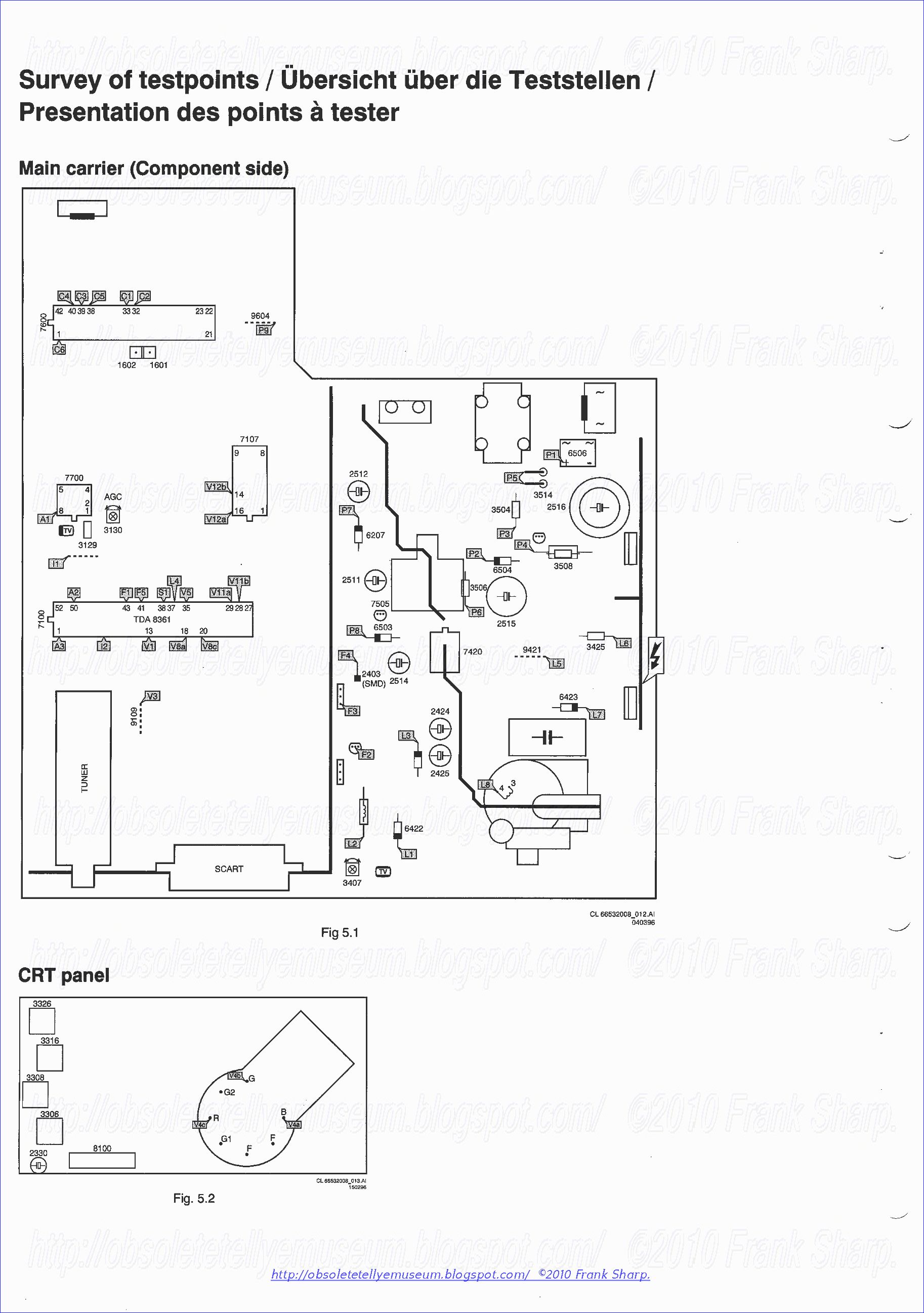
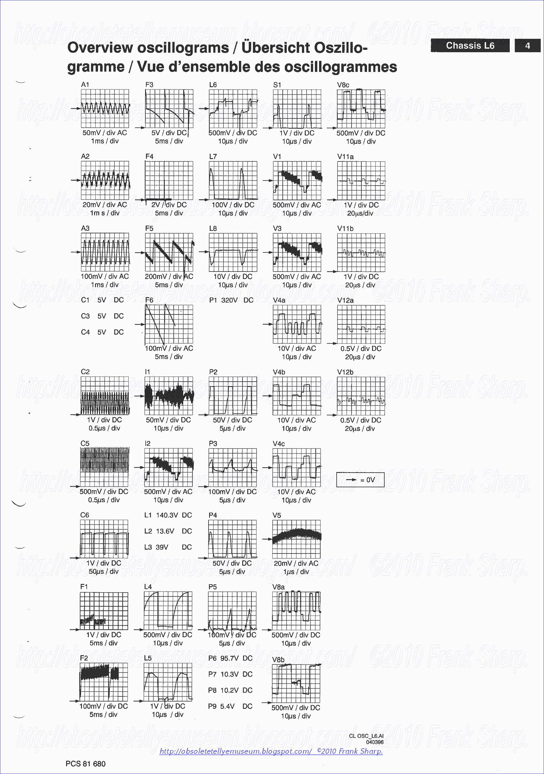
PHILIPS 14PT1363 CHASSIS L6.1 Picture display apparatus with a cathode ray tube and a self-oscillating switched-mode power supply:
PHILIPS developed a small effective minimalistic power supply:
A picture display apparatus includes a non-synchronized self-oscillating switched-mode power supply (SMPS) associated with a line output stage (35) which generates power supply voltages for other elements of the apparatus, the standby state being obtained by stopping the line scan. The switch (1) of the SMPS is a MOS-type field effect transistor, and it is turned on by a winding (6) which is magnetically coupled to a ballast inductance (5), this winding (6) having one end connected to the connection point (50) between the switch and the ballast inductance, and generates, at its other end (51), a control voltage which is in phase opposition with the voltage generated in the ballast inductance, the control voltage being transmitted to the gate of the field-effect transistor (1). A capacitor (42) is arranged as a shunt across the drain-source path of the FET and creates an oscillating circuit together with the ballast inductance (5).

1. A picture display apparatus comprising:
a DC voltage source for supplying a DC voltage between a first terminal and a second terminal, said DC voltage source rectifying a line voltage;
a cathode ray tube;
a standby device which remains active in a standby state of the apparatus; and
a self-oscillating switched-mode power supply connected to the first and second terminals of the DC voltage source, wherein said self-oscillating switched-mode power supply comprises:
a switch having an input coupled to the first terminal, said switch being a MOS-type field-effect transistor;
a ballast inductance having a first end coupled to an output of said switch;
an output stage of a line-scanning circuit having a first terminal coupled to a second end of the ballast inductance, and a second terminal coupled to the second terminal of the DC voltage source, said output stage of the line-scanning circuit being supplied by the self-oscillating switched-mode power supply, and, in turn, generating power supply voltages for different elements of the picture display apparatus;
a storage capacitance coupled between the second end of the ballest inductance and the second terminal of the DC voltage source in parallel to the output stage of the line-scanning circuit; and
an arrangement for switching ON and OFF the switch, the standby state being obtained by de-activating the line output stage while the switched-mode power supply is always active and supplies power to the standby device;
characterized in that said arrangement for switching ON and OFF the switch comprises:
a winding magnetically coupled to the ballast inductance, said winding having a first end connected to a connection point between said switch and the ballast inductance so as to generate, at a second end of the winding, a control voltage which, with respect to the connection point, is in phase opposition with a voltage generated in the ballast inductance;
a first capacitor coupling said second end of the winding to a gate of the MOS-type field-effect transistor for applying said control voltage to the gate for maintaining the switch conductive during each period of conductance, and for maintaining the switch non-conductive during each period of non-conductance;
a second capacitor arranged as a shunt across the drain-source path of the MOS-type field-effect transistor, for generating a free-oscillation with the inductance of the windings, then rendering said switch conductive after a given delay of non-conductance; and
means for measuring a current through said switch, and for turning the switch OFF when the measured current exceed a predetermined value, at the end of each period of conductance.
2. A picture display apparatus as claimed in claim 1, characterized in that the means for measuring the current and for turning OFF the switch comprises a current measuring resistor connected in the main current path of the switch, and a circuit for shorting the gate of the MOS-type field-effect transistor to the second terminal of the DC source when the voltage across said current measuring resistor exceeds a predetermined value.
3. A picture display apparatus as claimed in claim 2, characterized in that the shorting circuit comprises a blocking transistor having a main current path arranged in series with a resistor between the gate of the MOS-type field-effect transistor and the second terminal of the DC source, and a base-emitter path coupled to the current-measuring resistor.
4. A picture display apparatus as claimed in claim 3, characterized in that said picture display apparatus further comprises a control circuit connected between a terminal carrying the power supply voltage for the line output stage, and a base of the blocking transistor.
5. A picture display apparatus as claimed in claim 1, characterized in that the standby circuit is fed from a rectifier arrangement connected to an additional winding which is magnetically coupled to the ballast inductance.
6. A picture display apparatus as claimed in claim 3, characterized in that said arrangement for switching ON and OFF the switch comprises means for turning the switch ON, said turning ON means comprising a resistor in series with said first capacitor.
Description:
BACKGROUND OF THE INVENTION
1. Field of the Invention
The invention relates to a picture display apparatus with a cathode ray tube, comprising a standby device which remains active in a standby state of the apparatus, and a self-oscillating switched-mode power supply (SMPS) comprising, in cascade between two terminals of a source of direct current obtained by line voltage rectification, a switch, a ballast inductance, and the supply current path of a line output stage which generates power supply voltages for different elements of the device to be insulated from the line voltage, the standby state being obtained by stopping the line scan while the SMPS is always active and feeds the standby device, the SMPS switch, which has successive periods of conductance and non-conductance, being rendered non-conducting at the end of each period of conductance by means of a blocking arrangement which measures the current in the switch and controls the operation of rendering said switch non-conducting when the measured current exceeds a predetermined value.
The invention is applicable, inter alia, in the field of television and monitors.
2. Description of the Related Art
An SMPS is known from U.S. Pat. No. 4,788,591. It comprises a blocking arrangement which measures the current in the switch and controls the operation of rendering this switch non-conducting when the measured current exceeds a predetermined value. The assembly controlling the successive periods of conductance and non-conductance is, however, relatively complex.
SUMMARY OF THE INVENTION
It is an object of the invention to simplify the control in such a way that a control at both low cost and great reliability is obtained.
To this end, the switch, being a MOS-type field-effect transistor, is turned on at the start of each period of conductance by means of a winding which is magnetically coupled to the ballast inductance, this winding having one end connected to a connection point between the switch and the ballast inductance so as to generate, at its other end, a control voltage which, with respect to the connection point, is in phase opposition with the voltage generated in the ballast inductance, said control voltage being transmitted to the gate of the field effect transistor via a first capacitor, while a second capacitor is arranged as a shunt across the drain-source path of the field effect transistor.
The terminal of the DC source connected to the field-effect transistor being referred to as first terminal, the blocking arrangement is preferably connected between the gate of the MOS transistor and the second terminal of the DC source, and comprises a current-measuring resistor which is inserted between the line output stage and the second terminal, the blocking arrangement being advantageously constituted essentially by a blocking transistor having its main current path between the gate of the MOS transistor and the second terminal of the DC source, and its base-emitter path coupled to the current-measuring resistor.
The blocking arrangement and the means for rendering the switch conducting thus cooperate in a simple manner.
The apparatus advantageously comprises a control circuit connected between a terminal which holds the power supply voltage of the line output stage and the base of the blocking transistor.
The blocking arrangement and the control circuit thus cooperate in a simple manner.
The standby circuit is advantageously fed from a rectifier arrangement connected to an additional winding which is magnetically coupled to the ballast inductance.
This ensures power supply of the standby circuit during the standby periods.
These and other aspects of the invention will be apparent from and elucidated with reference to the embodiments described hereinafter.
BRIEF DESCRIPTION OF THE DRAWINGS
In the drawings:
FIG. 1 shows diagrammatically, a picture display apparatus with a cathode ray tube and a line output stage, a standby device and a self-oscillating switched-mode power supply (SMPS);
FIG. 2 shows diagrammatically, a self-oscillating SMPS; and
FIG. 3 shows curves to illustrate the operation of the SMPS and,
FIG. 4 shows diagrammatically, a control module suitable for controlling the SMPS.
DESCRIPTION OF THE PREFERRED EMBODIMENTS
 The invention will be described with reference to a television set, but it is also applicable to any other picture display apparatus, for example, a monitor.
The television set, which is shown in a diagram in FIG. 1, comprises a tuner 22 for receiving a signal, for example, from an antenna 37 and for transposing the frequency of the apparatus to intermediate frequencies intended for a subsequent IF video amplifier 23 and an IF audio amplifier 24. The IF audio amplifier 24 is followed by a demodulator 29 which supplies the audio signals in the baseband to an audio output amplifier 27 feeding a loudspeaker 33. The IF video amplifier 23 is followed by a unit video processor/sync. separator 25 which supplies a video signal in the baseband to a video amplifier 26 supplying the signals ad hoc to the electrodes of a cathode ray tube 32. The video processor/sync. separator unit 25 also extracts, from the signal, synchronizing signals which are applied to a line scanning circuit 36 and a field scanning circuit 28. The field scanning circuit 28 supplies a current in a field deflection coil 30. The line scanning circuit 36 comprises an output stage 35 which supplies a current in a line deflection coil 34 and generates a voltage, referred to as "extra-high tension" (EHT) of approximately 25 kV for supplying power to the screen of the display tube via a connection 31. The line output stage 35 is fed via a connection 49 by a self-oscillating switched-mode power supply circuit 38 which itself is DC-fed by a DC soure 39 of known type which can be connected to the line voltage by means of a current terminal 43 and is essentially constituted by a rectifier assembly and a storage capacitor. The other circuits 22-29, which must be insulated from the line voltage are fed in known mariner from the line output stage 35 through connections which, for the purpose of simplifying the Figure, are not shown. The switched-mode power supply 38 is not synchronized with the line frequency. A standby device 48, which remains active in a standby state of the apparatus, is directly fed by the SMPS 38. The standby state is obtained by stopping the line output stage 35, which suppresses the supply of the circuits 22-29 from the line output stage 35, while the SMPS 38 is always active and feeds the standby device 48.
The SMPS of FIG. 2 corresponds to the SMPS 38 of FIG. 1. The DC source 39 in FIG. 1 provides a voltage Vs of about 300 V, obtained by a rectifier bridge if the mains is 220 V, or by a doubler in the case of 110 V. This voltage is applied between a first terminal 20 and a second terminal 21, with its positive pole, for example, at the terminal 20. The polarity types of the semiconductors mentioned hereinafter are derived from this polarity.
The power supply comprises, in cascade from the terminal 20, a switch consisting of an N-channel, enhancement-mode MOS field-effect transistor 1, and a ballast inductance 5 connected to a power supply input of the line output stage 35 in which the power supply current path ends at the terminal 21. The line output stage 35 is shunted by a storage capacitor 4 and the assembly consisting of the line output stage 35 in cascade with the winding 5 is shunted by a recovery diode 2. The operation of the elements 1, 5, 4, 2, 35 mentioned above is well known. The power supply voltage supplied to the line output stage 35 is, for example, 100 V.
The switch for the SMPS, namely the transistor 1, has successive periods of conductance and non-conductance. The operation of rendering it non-conducting is controlled by a blocking arrangement which measures the current and controls the blocking of transistor 1 when the measured current exceeds a predetermined value. This arrangement is essentially constituted by transistor 10 of the NPN type, referred to as blocking transistor, having its main current path between the gate of MOS transistor 1 and the second terminal 21 of the DC source, in series with a resistor 13, and having its base-emitter path connected to a current measuring resistor 8 which is inserted between the line output stage 35 and the second terminal 21. The current which flows through the resistor 8 is substantially the same as that which flows through the transistor 1. The voltage generated by the current in the resistor 8 is transmitted to the base 53 of the transistor 10 via a resistor 7.
One end of a winding 6, which is magnetically coupled to the ballast inductance 5, is connected to the point 50 between a transistor 1 and the inductance 5. This winding is coiled in such a sense that it generates, between its other end 51 and the point 50, a control voltage which is in phase opposition with the voltage generated in the ballast inductance, i.e., with the voltage between the point 49 and the point 50. The other end 51 is connected to the gate of the field-effect transistor via a first capacitor 12 in series with a resistor 11. A second capacitor 42 is arranged as a shunt onto the drain-source path of the field-effect transistor.
The standby circuit 48 shown in FIG. 1 is supplied by a terminal 44 of the SMPS from a rectifier arrangement consisting of a diode 45 and a storage capacitor 47 connected to an additional winding 46 which is magnetically coupled to the ballast inductance 5.
The operation of this assembly will be explained with reference to the characteristic curves in FIG. 3 and the diagram in FIG. 2. Let it be assumed that the transistor 1 is turned on. The voltage at the point 50 in FIG. 2, indicated by the reference numeral 16 in FIG. 3, is 300 V: if neglecting the voltage at the terminals of the transistor 1, the terminal 49 is at 100-300=-200 V with respect to the terminal 50. As the windings 5 and 6 operate as a transformer, a positive voltage is generated at the point 51 with respect to the point 50. This voltage, transmitted to the gate of transistor 1 by the capacitor 12 and the resistor 11, maintains the transistor 1 conducting. The voltage at the terminals of the inductance 5, between the point 50 and the point 49, being fixed, the current in this inductance 5, indicated by the reference numeral 19, and also flowing in the transistor 1 and in the resistor 8, has an approximately linear growth. Let it be assumed, for example, that the resistor 8 has a value of 0.56 ohm. When the current reaches approximately 1.8 amperes, it will develop a voltage of 1 Volt which, via the resistor 7, renders the transistor 10 conducting. The lower end of the resistor 13 then decreases to almost zero volt. The voltage applied to the gate of transistor 1 is that of the left plate of the capacitor 12 but is decreased by the divider bridge effect of the resistors 11 and 13. The transistor 1 becomes non-conducting. At this instant, the current in the inductance 5, which cannot disappear in one go, ends via the recovery diode 2 which becomes conducting. The voltage at the point 50 therefore decreases to approximately -0.8 V. Thus, there is approximately 101 V between the terminal 49 and the terminal 50. As the windings 5 and 6 always operate as a transformer, a negative voltage is generated at the point 51 with respect to the point 50. This voltage, transmitted to the gate of transistor 1, confirms and reinforces the blocking operation. As the current no longer flows in the resistor 8, the transistor 10 becomes non-conducting again and the voltage again builds up at its collector, but as a consequence of the voltage applied by the winding 6, this does not render the transistor 1 conducting. From this instant, the current, indicated by the reference numeral 14, decreases in an approximately linear manner. When it has become zero, the capacitor 42 will start resonating with the inductance 5, which triggers a free oscillation; the reference numeral 15 shows what this oscillation would look like if it could last. However, when the voltage at the point 50 exceeds 100 V, i.e., when it becomes higher than the voltage at the point 49, a positive voltage will again be induced at the point 51, this voltage being transmitted to the gate of transistor 1 and rendering this transistor conducting. The oscillation 15 is then stopped and the voltage at the point 50 builds up to 300 V, as indicated at 18.
A control circuit 41 is connected between the terminal 49, having the power supply voltage of the line output stage, and the connection to the base 53 of the blocking transistor 10. This circuit, which is of a known type and is based on the comparison between a voltage of a zener diode and a fraction of the power supply voltage, is illustrated in FIG. 4. It comprises, between the terminal 49 and ground, two cascade arrangements: that of a zener diode 58 and a resistor 57, and that of a controllable resistor 55 and a resistor 56. The junction point of the first-mentioned cascade arrangement is connected to the emitter of a transistor 54 of the PNP type, and the junction point of the secondly mentioned cascade arrangement is connected to the base of this transistor, whose collector is connected via a resistor 59 to the base 53 of the transistor 10 in FIG. 2. With the zener diode being for example, a 5 V model, the emitter voltage of transistor 54 is of about 95 V which is higher than the base voltage of the transistor 10 in FIG. 2. The transistor 54 thus adds a DC current in the resistor 7, this DC current shifting the triggering threshold of the transistor 10.
In a satisfactory embodiment, the power supply comprises the following essential components:
transistor 1=BUK444, transistor 10=BF487, transistor 54=BF423,
diode 2=BYD34, zener diode 58=BZX79-C5V6
capacitor 42=330 pF, capacitor 12=33 nF,
resistor 11=1.8 kΩ, resistor 13=6.8 kΩ, resistor 8=0.56 Ω, resistor 7=330 Ω, resistor 57=33 kΩ, resistor 55=10 kΩ, resistor 56=100 kΩ, resistor 59=10 kΩ.
The line output stage 35 may be de-activated by known means which does not form part of the invention, in such a way that the module 35 no longer supplies voltages to the other elements 22-28 in FIG. 1, with the effect that the apparatus is in a standby state and that the line output stage consumes hardly any current. The known means in question may consist of, for example, a control for the user who, by means of an opto-coupler inserted in a signal connection of the line output stage, interrupts this signal and stops the scan. The currents in the power supply are then very small, but the control circuit 41 maintains the voltage of 100 V, and as that of 300 V is always also present, the voltage at the terminals of the inductance 5 remains unchanged and thus also the voltage at the terminals of the winding 46; the standby circuit 58 is always supplied with the same voltage.
Inventors:
Decraemer, Alain (Garches, FR)
Dormet, Jean-claude (Chaville, FR)
U.S. Philips Corporation (New York, NY)
TDA8361 Integrated PAL and PAL/NTSC TV processor
PHILIPS TDA8362 (TDA8361) MAIN CHARACTERISTICS
The TDA8362 television processor microcircuit contains an intermediate
frequency (IF) signal processing circuit, a multi-standard demodulator
of a frequency-modulated sound signal, automatically tuned notch and
band-pass filters in the video signal processing channel, a luminance
signal delay line, a color signal decoder in the PAL and NTSC system
with automatic detection systems, TV / AV input selector, RGB signal
switching scheme, horizontal and vertical scanning synchronization
circuits.
Variant TDA8362A also contains automatic white balance circuits. Thus, the TDA8362 includes all the basic low signal circuits needed to build a color television receiver.
The minimum number of elements connected to external circuits and only
one element requiring adjustment (reference circuit of the IF signal
demodulator) creates an exceptional usability of the TDA8362. As a result, the TDA8362 processor has become one of the most widely used chips in modern television technology.
The main characteristics of TDA8362 are given in table. 1.
| Parameter | Value |
|---|---|
| Supply voltage | 8 ± 0.8 |
| Current consumption, mA | 80 |
| Power consumption | 0.7 |
| Sensitivity of the IFI, μV | 70 |
| Sensitivity UPCHZ, mV | 1 |
| Sound signal from an external input, mVeff | 350 |
| Video signal from external input, Vp_p | 1 |
| Signals at the inputs in RGB, Bn n | 0.7 |
| Demodulated PTsTS, Vp-p | 2,4 |
| Tuner AGC control current, mA | 0 ... 5 |
| The range of voltage changes AFCG, V | 6 |
| Audio output signal (vyv. 50), mV | 700 |
| Output signals in RGB, Bn_n | 4 |
| Horizontal line output current, mA | 10 |
| Framing output current, mA | 1 |
| Control voltage range, V | 0 ... 5 |

The latter contains a circuit for automatic white balance, the measuring signal at the input of which comes from pin 14 of TDA8362.
| TDA8362 | TDA8362A | Pin assignment |
|---|---|---|
| 1 | 1 | Pre-emphasis correction of sound signal and switching to positive modulation |
| 2 | 2 | IF signal demodulator reference circuit |
| 3 | 3 | IF signal demodulator reference circuit |
| 4 | 4 | Video identification circuit output, sound switch input |
| 5 | 5 | IF signal input and volume control |
| 6 | 6 | Audio input from external connectors |
| 7 | 7 | PCTS output |
| 8 | 8 | Decoupling capacitor of the power supply circuit of the digital part |
| 9 | 41 | Earth 1 (common) |
| 10 | 10 | Power input |
| eleven | eleven | Earth 2 (common) |
| 12 | 12 | Decoupling capacitor filter settings |
| thirteen | thirteen | Internal video input |
| 14 | 14 | RF correction circuit adjustment input (sharpness) |
| fifteen | fifteen | External video input |
| 16 | 16 | Chroma input |
| 17 | 17 | Brightness adjustment |
| 18 | 18 | Exit to |
| 19 | 19 | Output G |
| 20 | 20 | Output R |
| 21 | 21 | RGB switch and blanking output |
| 22 | 22 | Signal output R (from external sources) |
| 23 | 23 | Signal output G (from external sources) |
| 24 | 24 | Signal output B (from external sources) |
| 25 | 25 | Contrast adjustment |
| 26 | 26 | Saturation Adjustment |
| 27 | 27 | Color tone adjustment (or color signal output) |
| 28 | 28 | CV input BY (from delay line) |
| 29th | 29th | RRS input RY (from delay line) |
| thirty | thirty | RCS RY output (to delay line) |
| 31 | 31 | TsRS BY output (to the delay line) |
| 32 | 32 | 4.43 MHz reference signal output on TDA8395 |
| 33 | 33 | Phase detector filter |
| 34 | 34 | Conclusion connection of a quartz resonator of 3.58 MHz |
| 35 | 35 | 4.43 MHz quartz resonator connection terminal |
| 36 | 36 | Power output to trigger horizontal scanning |
| 37 | 37 | Horizontal scan trigger output |
| 38 | 38 | Horizontal Flyback Pulse Input / Gating Pulse Output (SSC) |
| 39 | 39 | Phase Detector Filter 2 |
| 40 | 40 | Phase Detector Filter 1 |
| 41 | 42 | Frame Reverse Pulse Input |
| 42 | 43 | Conclusion conclusion of an RC chain of ZG frame scan |
| 43 | 44 | Firing trigger pulses output |
| 44 | 9 | AFC output |
| 45 | 45 | IF signal input 1 |
| 46 | 46 | IF signal input 2 |
| 47 | 47 | AGC circuit output |
| 48 | 48 | A conclusion of the connection of the decoupling capacitor of the AGC circuit |
| 49 | 49 | Tuner AGC adjustment input |
| fifty | fifty | Sound output |
| 51 | 51 | Conclusion connection output decoupling capacitor demodulator sound |
| 52 | 52 | Decoupling capacitor of the power control circuit |
IF SIGNAL PROCESSING CIRCUIT The IF image signal amplifier (IFI) is a three-stage differential amplifier with an adjustable gain and a symmetrical differential input (vyv. 45 and 46 TDA8362). The gain variation range is at least 64 dB. The sensitivity of the IFI (70 μV) is comparable to the parameters of modern specialized TDA8362 IFI.
Maximum input signal up to 100 mV eff. The IF signal is demodulated using a reference carrier frequency generated by passive regeneration of the carrier image. The reference circuit of the demodulator is connected to pin 2 and 3 of the TDA8362. It is the only item that needs to be configured. The demodulator provides the ability to process IF signals with both negative and positive modulation. The automatic frequency control circuit (AFC) generates a signal at pin 44 of TDA8362, which provides tuning of the tuner local oscillator frequency with an error of no more than 50 kHz.
The circuit uses the same reference signal as for the demodulator.
The built-in sampling-storage circuit ensures the protection of the AFC circuit from the penetration of a video signal. A storage capacitor is built into the TDA8362. The steepness of the characteristics of the AFC circuit (33 mV / kHz) directly depends on the quality factor of the reference circuit. To reduce the steepness, a resistor is connected to pin 44 of the TDA8362. The output voltage range is 6 V (at a nominal frequency of 3.5 V). The characteristic of the AFC for the TDA8362-N5 modification is optimized for the European IF standard. The automatic gain control (AGC) circuit generates the control voltage of the amplifier and the tuner (vv. 47 TDA8362), ensuring a constant amplitude of the signals at the input of the amplifier and at the output of the video amplifier.
To exclude the influence of the AGC circuit on the tuner at low levels of the input signal, an AGC response delay is introduced. The delay value is regulated by applying a control voltage to pin 49 of the TDA8362. The voltage variation range is 0.5 ... 4.5 V. The minimum and maximum signal levels at pin 49, at which the tuner AGC is triggered, are 0.2 mV eff and 150 mV eff, respectively.
The AGC detector monitors the amplitude of the clock pulses with negative modulation of the IF signal and white peaks with positive modulation. To ensure noise immunity, the gating of the detector is used. Gating is disabled for the duration of the reverse frame scan. This allows you to avoid changing the amplitude of the video signal in the playback mode from the VCR due to phase shifts that occur during the switching of video heads. A capacitor (usually 2.2 μF) is connected to pin 48 of the TDA8362, which sets the time constant of the AGC circuit.
Switching the demodulator and the AGC circuit to the IF signal processing mode with positive modulation is carried out by supplying voltage (U pit -1) V to pin 1 of TDA8362. The video signal identification circuit works independently of the synchronization circuit, which ensures that the setting is saved to the received television channel during translation TV to monitor mode.
The circuit generates the following signals at the output (pin 4 of TDA8362):
- voltage no more than 0.5 V in the absence of a video signal (in this case, the sound detector is turned off);
- voltage of 6 V when receiving a signal with a frequency of a subcarrier of color of 3.58 MHz;
- voltage of 8 V when receiving a signal with a frequency of a subcarrier of color 4.43 MHz.
The signal amplitude at the output (pin 7 of TDA8362) is 2.4 V. The output impedance of the amplifier is not more than 50 Ohms, the load current is not more than 5 mA. The bandwidth of the video amplifier (at the level of -3 dB) is up to 9 MHz, which makes it possible to use TDA8362 in all broadcasting standards. The emission control scheme provides the inversion of white peaks exceeding 4.8 V, noise emissions having a level below 1.4 V (the tops of the clock pulses have a level of 2 V), and their introduction into the video signal at 3.2 V and 2.6 V , respectively. At the same time, the noise emission inversion circuit only works during the reception of a large signal, since with a weak signal it negatively affects the operation of the audio signal processing channel.
In the modification of TDA8362-N4, an ultra-white peaks binding scheme is used in the video signal. The TDA8362-N5 modification does not use a white peak limiting scheme, since when there are a large number of white peaks, inverting and introducing them at 3.2 V results in the image becoming gray.
The IF signal of the sound is limited and fed to the demodulator, made in the form of a phase locked loop (PLL). The PLL system is automatically tuned to the input frequency and does not require adjustments. The PLL system capture range is 4.2 ... 6.8 MHz.
The preliminary amplifier (PU) provides amplification of the detected sound signal to a level of 350 mV eff. This signal, which is not adjustable in magnitude, is fed to pin 1 of the TDA8362, to which an external capacitor is connected to correct the distortion of the sound signal, and to the switching and volume control circuitry. PU also provides mute when there is no identification of the video signal.
The signal from pin 1 of the TDA8362 is used to output to external connectors (for example, SCART). The sound signal from external connectors is fed to pin 6 of the TDA8362, its magnitude is 350 mV eff. The switching circuit, controlled by the voltage supplied to pin 16 of the TDA8362, provides for the output of pin 50 of the TDA8362 sound output signal, which then goes to the low-frequency amplifier.
The value of the output signal, which is -6 dB from the maximum is 700 mB eff, when adjusting the volume changes in the range of 80 dB. DC voltage at the terminal 50 TDA8362 3.3 V (when turning off the sound 10 ... 50 mB). The TDA8362-N5 modification provides click protection in the speakers when the sound is turned on, while using the previous TDA8362 modifications, a 290 kOhm resistor was needed between pin 1 of the TDA8362 and the +8 B bus to solve this problem.
Switching the TDA8362 to the signal processing mode with positive modulation is carried out by supplying at least 1 (U pit - 1) V to pin 1 of the TDA8362.
Lower case SIs are supplied to the first phase detector (PD1) and a coincidence detector, which identifies the presence of a video signal and controls the synchronization of the master oscillator (ZG) of horizontal scanning. In the absence of synchronization, the voltage at pin 14 of the TDA8362 becomes low, which can be used to identify the presence of a video signal. PD1, together with a low-pass filter (LPF) connected to pin 40 of TDA8362, and a horizontal scan line generator form a PLL that provides frequency and phase adjustment of the pulse pulses to lower case SI parameters.
The time constant ФД1 is automatically switched (by switching internal resistance) according to the signals from the noise detector and from the coincidence detector. With an increase in the noise level in the video signal at pin 13 of TDA8362, the PD1 time constant increases (the output current is 30 μA). In the absence of a video signal, the time constant increases even more (output current 6 μA), which ensures synchronization in the on-screen display (OSD) mode.
When a normal signal is received, as well as when processing a signal fed to pin 15 of the TDA8362, the time constant decreases (output current 180 μA) to expand the capture band and increase the noise im
munity of the synchronization circuit. To ensure quick compensation of the phase error that occurs in the signal from the VCR when switching the video heads, the time constant is further reduced by about 1.5 times for the reverse scan time of the vertical scan (output current 270 μA). Thus, good synchronization circuit characteristics are achieved both in the case of receiving a weak signal and in the case of signal processing from a VCR.
The video signal span on pin 13 of the TDA8362 (including sync pulses) must be at least 2 V when a normal signal is received. Otherwise, the noise detector will switch the time constant at a lower IF signal level (switching occurs at a signal-to-noise ratio of 20 dB), which will lead to a “jitter” phase of the horizontal scanning signal.
To ensure the independence of the image phase from the horizontal frequency (15.625 or 15.734 kHz), the PD1 static characteristic has a very high slope. Horizontal scanning operates at a double horizontal scanning frequency. Its frequency is automatically calibrated using the tuning circuit by comparing it with the frequency of the generator with quartz stabilization of the color decoder. As a result, the frequency of free oscillations of the GB has a deviation of no more than 2% of the central value. At startup, calibration is always performed with 4.43 MHz quartz, unless the 3.58 MHz quartz forced mode is selected.
The second phase detector (FD2) ensures the formation of horizontal line triggering pulses on pin 37 of the TDA8362 and maintaining the phase of these pulses relative to 3G pulses in the capture mode in PD1. PD2 together with the low-pass filter connected to pin 39 of the TDA8362 and the 3G form a PLL. The initial phase of the image is set by changing the external load connected to pin 39 of TDA8362. The shift range is ± 2 μs when the control current changes within ± 6 μA. The horizontal flyback pulses necessary for the operation of PD2 are received at pin 38 of TDA8362.
At the same output, combined strobe pulses are formed, which are necessary for operation of integrated delay line microcircuits (TDA4661 or TDA4665) and SECAM decoder (TDA 8395).
Gating pulses have the following parameters:
- binding voltage during the reverse pulse: 3 ± 0.4 V;
- voltage during the quenching pulse: 2 ± 0.2 V;
- voltage during the color subcarrier flash: 5.3 ± 0.5 V;
- field blanking pulse width: 14 lines;
- flash highlight pulse width: 3.5 ± 0.2 μs.
Parameters of pulses of start of horizontal scanning:
- lower level of output voltage: 0.3 V;
- maximum level: U pit;
- pulse duty cycle: 2;
- maximum permissible output current: 10 mA.
In TDA8362-N5, the maximum trigger pulse frequency is limited to 20 kHz. When the voltage on pin 36 of TDA8362 decreases to 5.8, the formation of start pulses immediately stops. If the pre-start mode of the ЗГ is not used, then pin 36 and 10 of the TDA8362 are connected to the 8 V power bus. With separate power supply, the voltage at pin 36 must always be greater than or equal to the voltage at pin 10 of the TDA8362.
The control pulses for the HR horizontal scan, which is a sawtooth voltage generator, are obtained by dividing the frequency of the horizontal horizontal scan.
The frequency divider has two operating modes.
The “large window” mode is activated when there is no synchronization or when a non-standard signal is received (the number of lines in a half-frame is from 311 to 314 in 50 Hz mode and from 261 to 264 in 60 Hz mode). In this case, the divider is in search mode and switches from a frequency of 45 Hz to a frequency of 64.5 Hz.
The narrow window mode is activated when more than 15 consecutive frame sync pulses are detected.
This is the standard mode of operation. In the absence of clock pulses, the reverse motion of Zr turns on at the end of the half-frame (window), which ensures minimal image distortion.
The divider switches back to search mode if there are no frame sync pulses for 6 consecutive periods of frame scan. To pin 42 of TDA8362 is connected an external RC chain of a 3G frame scan.
The amplitude of the sawtooth voltage at pin 42 is 1.5 ... 1.8 V. At pin 41 of the TDA8362, reverse-frequency pulses of a vertical sweep (from the output stage) are applied to ensure the linearity of the output voltage.
The constant voltage on pin 41 is 2.5 ± 0.5 V, the alternating voltage is 1 V. In the TDA8362, the kinescope is protected against burn-through in the event of a frame scan failure, which dampens the rays when the direct voltage on pin 41 of the TDA8362 increases or decreases by 1 5 in (relative to the above). Framing control pulses are formed on pin 43 of TDA8362. The maximum and minimum voltage are respectively 4 and 0.3 V.
The maximum permissible output current is 1 mA. The delay in turning on the vertical scan at power-on is 140 ms, and the output voltage is high. When you start the HR frame scan is turned on at a frequency of 60 Hz.
In the TDA8362-N5 modification, the launch is carried out at a frequency of 50 Hz, which is used for the on-screen display. The voltage at pin 43 of the TDA8362 when turned on is low, which makes it easier to start the frame sweep.
TDA8362 synchronization circuit The TDA8362 provides reliable horizontal and frame synchronization of the image when processing a signal from a VCR, both in the case of phase displacement of the clock pulses (with a stretched tape), and in the case of playing back video tapes with copy protection.
TDA8362 VIDEO PROCESSING CIRCUIT
The full color television signal allocated on pin 7 of the TDA8362 passes notch filters to suppress the second intermediate frequency of the sound and goes to pin 13 of the TDA8362 (internal signal). On pin 15 of the TDA8362, a signal is supplied from external inputs (external signal).
The signal swing at pin 13 (including sync pulses) is 2 ... 2.8 V, and at pin 15 is TDA8362 1 ... 1.4 V. Switching the input video signal is carried out by a switching circuit controlled by voltage level on pin 16 of TDA8362 (U 16). At U 16 <0.5B, internal video and audio signals are processed (a notch filter that suppresses the color signal is turned on). With 3 <U16 <5V, external video and audio signals in the S-VHS standard are processed. In this case, a color signal is supplied to pin 16 of the TDA8362, and a brightness signal to pin 15. The notch filter is disabled in this mode. At U16> 7.5 V, external video and audio signals are processed (notch filter on).
The TDA8362 contains notch and bandpass filters to separate color and luminance signals.
The filter tuning scheme provides automatic adjustment of the filters in accordance with the frequency of the crystal oscillator included in the decoder. A pin 12 of the TDA8362 is connected to a decoupling capacitor of the tuning circuit.
In modification TDA8362-N5, the resonant frequency of the notch filter during signal processing in the SECAM system is reduced to 4.2 MHz to provide better suppression of the DR and DB subcarriers in the luminance signal. Filters are calibrated during the reverse frame scan. The luminance signal enters the delay line (480 ns) and the RF correction circuit, which provides an increase in the frequency response in the high-frequency region, and then to the matrixing circuit. pin 14 TDA8362 is used to control the RF correction circuit (image sharpness). The control voltage range is 0 ... 5 V. When a voltage of 7 V is applied to pin 14, the correction circuit is switched off (nominal mode). In the absence of a video signal, the current consumed by TDA8362 according to pin 14 increases to 1 mA (in versions N3 and N4 - up to 200 μA). The voltage on pin 14 is reduced. This information can be used to identify the video signal.
The color signal is fed to a band-pass filter and an amplifier with AGC, and then to a decoder, which includes a generator with quartz frequency stabilization, a color difference signal demodulator (CRS), and a color off circuit.
The generator generating the signal of the reference subcarrier, the PD, and the low-pass filter connected to pin 33 of the TDA8362 form a PLL system that provides synchronization in frequency and phase of the signals of the reference subcarrier with a color burst signal (SCC). Quartz resonators are connected to pin 34 and 35 of the TDA8362, while a resonator with a frequency of 4.43 MHz is connected to pin 35. This frequency is used for calibrating 3G horizontal scanning, and to pin 34 - a resonator with a frequency of 3.58 MHz.
When using one quartz or connecting two quartz to one pin (usually to pin 34) and using an external switching circuit, pin 35, the TDA8362 is connected to the power bus through a 47 kOhm resistor. This ensures the forced inclusion of the generator.
When using modifications N4 and N5 TDA8362, the value of the resistor is reduced to 8.2 kOhm. This is essential to enable 3G line scan calibration. The system's automatic detection circuitry provides recognition of color signals in PAL and NTSC systems and switching of signal processing circuits.
To process the color signal in the SECAM system, a TDA8395 decoder is used, to which a 4.43 MHz reference signal is supplied from pin 32 of the TDA8362. The amplitude of the reference signal is 0.25 ± 0.5 V. In the case of identifying a color signal in a PAL or NTSC system, the voltage at pin 32 of the TDA8362 is 1.5 V. If there is no identification, the color scheme disables the outputs of the demodulator central circuit (pin 30 and 31) , and the voltage on pin 32 of the TDA8362 increases to 5 V. This voltage blocks the TDA8395 color shutdown circuit in m / s and connects its outputs to the central control system.
The current consumed by TDA8395 with pin 32 of TDA8362 when identifying a color signal in the SECAM system is 150 μA. Increasing the current to this value forces the TDA8362 to SECAM mode. In this case, the system automatic detection circuit does not search for color signals in PAL and SECAM systems. Forcing the TDA8362 to NTSC mode is not possible.
The color signal for the TDA8395 can be obtained on pin 27 of the TDA8362 by connecting this output to the power bus via a 4.7 ... 12 kΩ resistor. The signal span is 330 mV. This combination of chips can only be used as a PAL / SECAM decoder. In the case of color signals processing, PAL / SECAM / NTSC systems use an external color signal extraction circuit for TDA8395.
It should be noted that when using modifications N4 and N5 of TDA8362, to prevent erroneous identification of the signal from the video recorder in the SECAM system as NTSC, it is necessary to provide a voltage at the terminal 27 of TDA8362 of at least 6 V.
FEATURES
Available in TDA8360, TDA836
1
and TDA8362
· Vision IF amplifier with high
sensitivity and good differential
gain and phase
· Multistandard FM sound
demodulator (4.5 MHz to 6.5 MHz)
· Integrated chrominance trap and
bandpass filters (automatically
calibrated)
· Integrated luminance delay line
· RGB control circuit with linear RGB
inputs and fast blanking
· Horizontal synchronization with two
control loops and alignment-free
horizontal oscillator without
external components
· Vertical count-down circuit
(50/60 Hz) and vertical preamplifier
· Low dissipation (700 mW)
· Small amount of peripheral
components compared with
competition ICs
· Only one adjustment (vision IF
demodulator)
· The supply voltage for the ICs is
8 V. They are mounted in a shrink
DIL envelope with 52 pins and are
pin compatible.
Additional features
TDA8360
· Alignment-free PAL colour decoder
for all PAL standards, including
PAL-N and PAL-M.
TDA8361
· PAL/NTSC colour decoder with
automatic search system
· Source selection for external
audio/video (A/V) inputs (separate
Y/C signals can also be applied).
TDA8362
· Multistandard vision IF circuit
(positive and negative modulation)
· PAL/NTSC colour decoder with
automatic search system
· Source selection for external
A/V inputs (separate Y/C signals
can also be applied)
· Easy interfacing with the TDA8395
(SECAM decoder) for
multistandard applications.
GENERAL DESCR
IPTION
The TDA8360, TDA8361 and
TDA8362 are single-chip TV
processors which contain nearly all
small signal functions that are
required for a colour television
receiver. For a complete receiver the
following circuits need to be added:
a base-band delay line (TDA4661),
a tuner and output stages for audio,
video and horizontal and vertical
deflection.
Because of the different functional
contents of the ICs the set maker can
make the optimum choice depending
on the requirements for the receiver.
The TDA8360 is intended for simple
PAL receivers (all PAL standards,
including PAL-N and PAL-M are
possible).
The TDA8361 contains a PAL/NTSC
decoder and has an A/V switch.
For real multistandard applications
the TDA8362 is available. In addition
to the extra functions which are
available in the TDA8361, the
TDA8362 can handle signals with
positive modulation and it supplies
the signals which are required for the
SECAM decoder TDA8395.
TDA8361
The TDA8361 has the following
differences to the pinning:
Pin 1: only audio de-emphasis
Pin 27: only hue control
Pin 32: 4.43 MHz output for TDA8395
is not connected.
FUNCTIONAL DESCRIPTION
Video IF amplifier
The IF amplifier contains
3 AC-coupled control stages with a
total gain control range of greater
than 60 dB. The sensitivity of the
circuit is comparable with that of
modern IF ICs.
The reference carrier for the video
demodulator is obtained by means of
passive regeneration of the picture
carrier. The external reference tuned
circuit is the only remaining
adjustment of the IC.
In the TDA8362 the polarity of the
demodulator can be switched so that
the circuit is suitable for both positive
and negative modulated signals.
The AFC circuit is driven with the
same reference signal as the video
demodulator. To ensure that the
video content does not disturb the
AFC operation a sample-and-hold
circuit is incorporated; the capacitor
for this function is internal. The AFC
output voltage is 6 V.
The AGC detector operates on levels,
top sync for negative modulated and
top white for positive modulated
signals.The AGC detector time
constant capacitor is connected
externally. This is mainly because of
the flexibility of the application.
The time constant of the AGC system
during positive modulation
(TDA8362) is slow, this is to avoid any
visible picture variations. This,
however, causes the system to react
very slowly to sudden changes in the
input signal amplitude.
To overcome this problem a speed-up
circuit has been included which
detects whether the AGC detector is
activated every frame period. If,
during a 3-frame period, no action is
detected the speed of the system is
increased. When the incoming signal
has no peak white information (e.g.
test lines in the vertical retrace period)
the gain would be video signal
dependent. To avoid this effect the
circuit also contains a black level
AGC detector which is activated when
the black level of the video signal
exceeds a certain level.
The TDA8361 and TDA8362 contain
a video identification circuit which is
independent of the synchronization
circuit. Therefore search tuning is
possible when the display section of
the receiver is used as a monitor. In
the TDA8360 this circuit is only used
for stable OSD at no signal input. In
the normal television mode the
identification output is connected to
the coincidence detector, this applies
to all three devices. The identification
output voltage is LOW when no
transmitter is identified. In this
condition the sound demodulator is
switched off (mute function). When a
transmitter is identified the output
voltage is HIGH. The voltage level is
dependen
t on the frequency of the
incoming chrominance signal.
Sound circuit
The sound bandpass and trap filters
have to be connected externally. The
filtered intercarrier signal is fed to a
limiter circuit and is demodulated by
means of a PLL demodulator. The
PLL circuit tunes itself automatically
to the incoming signal, consequently,
no adjustment is required.
The volume is DC controlled. The
composite audio output signal has an
amplitude of 700 mV RMS at a
volume control setting of -6 dB. The
de-emphasis capacitor has to be
connected externally. The
non-controlled audio signal can be
obtained from this pin via a buffer
stage. The amplitude of this signal is
350 mV RMS.
The TDA8361 and TDA8362 external
audio input signal must have an
amplitude of 350 mV RMS. The
audio/video switch is controlled via
the chrominance input pin.
Synchronization circuit
The sync separator is preceded by a
voltage controlled amplifier which
adjusts the sync pulse amplitude to a
fixed level. The sync pulses are then
fed to the slicing stage (separator)
which operates at 50% of the
amplitude.
The separated sync pulses are fed to
the first phase detector and to the
coincidence detector. The
coincidence detector is used for
transmitter identification and to detect
whether the line oscillator is
synchronized. When the circuit is not
synchronized the voltage on the
peaking control pin (pin 14) is LOW
so that this condition can be detected
externally. The first PLL has a very
high static steepness, this ensures
that the phase of the picture is
independent of the line frequency.
The line oscillator operates at twice
the line frequency.
The oscillator network is internal.
Because of the spread of internal
components an automatic adjustment
circuit has been added to the IC.
The circuit compares the oscillator
frequency with that of the crystal
oscillator in the colour decoder. This
results in a free-running frequency
which deviates less than 2% from the
typical value.
The circuit employs a second control
loop to generate the drive pulses for
the horizontal driver stage.
X-ray protection can be realised by
switching the pin of the second
control loop to the positive supply line.
The detection circuit must be
connected externally. When the X-ray
protection is active the horizontal
output voltage is switched to a high
level. When the voltage on this pin
returns to its normal level the
horizontal output is released again.
The IC contains a start-up circuit for
the horizontal oscillator. When this
feature is required a current of 6.5 mA
has to be supplied to pin 36. For an
application without start-up both
supply pins (10 and 36) must be
connected to the 8
V supply line.
The drive signal for the vertical ramp
generator is generated by means of a
divider circuit. The RC network for the
ramp generator is external.
Integrated video filters
The circuit contains a chrominance
bandpass and trap circuit. The filters
are realised by means of gyrator
circuits and are automatically tuned
by comparing the tuning frequency
with the crystal frequency of the
decoder.
In the TDA8361 and TDA8362 the
chrominance trap is active only when
the separate chrominance input pin is
connected to ground or to the positive
supply voltage and when a colour
signal is recognized.
When the pin is left open-circuit the
trap is switched off so that the circuit
can also be used for S-VHS
applications.
The luminance delay line and the
delay for the peaking circuit are also
realised by means of gyrator circuits.
Colour decoder
The colour decoder in the various ICs
contains an alignment-free crystal
oscillator, a colour killer circuit and
colour difference demodulators.
The 90° phase shift for the reference
signal is achieved internally. Because
the main differences of the 3 ICs are
found in the colour decoder the
various types will be discussed.
TDA8360
This IC contains only a PAL decoder.
Depending on the frequency of the
crystals which are connected to the IC
the decoder can demodulate all PAL
standards. Because the horizontal
oscillator is calibrated by using the
crystal frequency as a reference the
4.4 MHz crystal must be connected to
pin 35 and the 3.5 MHz crystal to
pin 34. When only one crystal is
connected to the IC the other crystal
pin must be connected to the positive
supply rail via a 47 kW resistor. For
applications with two 3.5 MHz
crystals both must be connected to
pin 34 and the switching between the
crystals must be made externally.
Switching of the crystals is only
allowed directly after the vertical
retrace. The circuit will indicate
whether a PAL signal has been
identified by the colour decoder via
the saturation control pin.
When two crystals are connected to
the IC the output voltage of the video
identification circuit indicates the
frequency of the incoming
chrominance signal.
The conditions are:
· Signal identified at
fosc = 3.6 MHz; VO = 6 V
· Signal identified at
fosc = 4.4 MHz (or no colour);
VO = 8 V.
This information can be used to
switch the sound bandpass filter and
trap filter.
TDA8361
This IC contains an automatic
PAL/NTSC decoder. The conditions
for connecting the reference crystals
are the same as for the TDA8360.
The decoder can be forced to PAL
when the hue control pin is connected
to the positive supply voltage via a
5 kW or 10 kW resistor
(approximately). The decoder cannot
be forced to the NTSC standard. It is
also possible to see if a colour signal
is recognized via the saturation pin.
TDA8362
In addition to the possibilities of the
TDA8361, the TDA8362 can
co-operate with the SECAM add-on
decoder TDA8395.
The communication between the two
ICs is achieved via pin 32. The
TDA8362 supplies the reference
signal (4.43 MHz) for the calibration
system of the TDA8395, identification
of the colour standard is via the same
connection. When a SECAM signal is
detected by the TDA8395 the IC will
draw a current of 150 mA. When
TDA8362 has not identified a colour
signal in this condition it will go into
the SECAM mode, that means it will
switch off the R-Y and B-Y outputs
and increase the voltage level on
pin 32.
This voltage will switch off the
colour-killer in the TDA8395 and
switch on the R-Y and B-Y outputs of
the TDA8395. Forcing the system to
the SECAM standard can be
achieved by loading
pin 32 with a
current of 150 mA. Then the system
manager in the TDA8362 will not
search for PAL or NTSC signals.
Forcing to NTSC is not possible.
For PAL/SECAM applications the
input signal for the TDA8395 can be
obtained from pin 27 (hue control)
when this pin is connected to the
positive supply rail via the 5 kW or
10 kW resistor. An external source
selector is required by the
TDA8395/TDA8362 combination for
PAL/SECAM/NTSC applications.
RGB output circuit
The colour difference signals are
matrixed with the luminance signal to
obtain the RGB signals. Linear
amplifiers have been chosen for the
RGB inputs so that the circuit is
suitable for incoming signals from the
SCART connector. The contrast and
brightness controls operate on
internal and external signals.
The fast blanking pin has a second
detection level at 3.5 V.
When this level is exceeded the
RGB outputs are blanked so that
“On-Screen-Display” signals can be
applied to the outputs.
The output signal has an amplitude of
approximately 4 V, black-to-white,
with nominal input signals and
nominal control settings. The nominal
black level is 1.3 V.
PHILIPS CHASSIS L6.1 L6.2TV REPAIR TIPS SERVICE FIND AND FAULT REPAIR.
Philips L6 series Dead Chopper FET, SOPS kit & HT smoother C2515 47µ 200v
Philips L6.1 After a while white screen. Check/replace LOT L5422.
Philips L6.1 Bad focus or focus varies in a new set or after CRT replacement Possible solution: Short circuit the focus and the G2 pins of the picture tube with the aquadag coating. Switch the set on for approximately 5 seconds. After this return the set to its original condition. Check if the focus adjusted normally. If not repla
Philips L6.1 Bending picture depending on its white contents. Change R3420 (see diagram A1) from 12k to 18K (service code 4822 116 52251)
IRIS CODE : 1353
Philips L6.1 Code-number supply-repair kit L6.1 Code-number supply-repair kit L6.1
In the service manual of the L6.1 the codenumber of the supply-repair
kit is missing. The code-number is 4822 310 10663.
Philips L6.1 Colour flashes appears or loss of chroma in SECAM standard Change R3433 (see Diagram A1) from 39K to 56K service code
4822 051 20563
Philips L6.1 Cracks in sound during fast changing of picture from black to white. Change C2425 to 2200uF 25V.codenumber 4822 124 42449.
REMARKS :
This only occurs if contrast is at maximum.
Philips L6.1 Cracks in sound during fast changing of picture from black to white. New solution: Replace 9001 by 39 Ohm NFR = 4822 052 10399 and add
470 uF between 9001/3013 and ground (470 uF=4822 124 80791)
Philips L6.1 Cross picture (You can partly see the picture of the next station) Add new Saw filter (CE marking module = 4822 212 11352). This filter
can be switched between BG and DK. How to adapt the set:
* remove saw filter on position 1001 and replace by CE marking
module.
* solder the black wire in the hole MCE1 near .P
Philips L6.1 Dead - chopper s/c, mains fuse o/c etc Fit repair kit - still dead with squealing from tfmr - pin hole in BUT11AX encapsulation (measured ok out of cct)
Philips L6.1 Does not find all programs during search (for TXT and NO-TXT versions) New software will solve this problem.
Change software into new version;codenumbers are still identical
4822 209 14646:TXT 1 p Mono Pan-European L6TXTMOEU-1.1
3/4 keys:SAA5290ZP/072
4822 209 15425:TXT 1 p Mono Greek/Turkisch L6TMOGT-1.1
Philips L6.1 Does not find all programs during search. Replace microprocessor IC7600 with version L6NOTXT-2.0,
codenumber 4822 209 13085.
Philips L6.1 Focus not optimal Check/replace LOT L5422.
Philips L6.1 Hotel mode Hotel mode
Only for L6.1 with 3 buttons
To activate/de-activate:
- select channel 38
- push OSD menu and select Hotel Mode
Philips L6.1 Hotel mode Hotel mode
Only for L6.1 chassis with 4 buttons
To activate this mode do the following:
- select channel 38
- push vol- and vol + on the TV set AND OSD on the remote control
simultaneously.
- you now enter the hotel mode.
To leave the hotel
Philips L6.1 Hotel mode, hospital1 mode, hospital2 mode Hotel mode, hospital1 mode, hospital2 mode
L6.1 chassis can be put in hotel-mode, hospital1 or hospital2 mode.
When the set is in a hospital mode, the set can leave this mode by
pushing the PIP on-off or the PIP
Philips L6.1 Inoperative (squeaking sound) Cause is defective LOT: 4822 140 10562
Probably the power supply is also defective:
4822 310 10663 Supply-kit.
Supply and EHT can be tested seperately by opening jumper 9420.
Philips L6.1 Lock up & lose pic int Mod reqd- replace Tr7505 BC548B with BC337-40; R3500 from 330R to 470R; if fault persists change EEPROM chip pt no 4822 2096 2098
Philips L6.1 No colour or colour flashes Change R3420 (see diagram A1) from 12k to 18K (service code 4822 116 52251)
Philips L6.1 No contrast Check/replace R3421 and R3420 (15K).
Philips L6.1 No function, but supply and LED are on Check contrast and brightness
Philips L6.1 No picture no sound, only red LED Check for brooken tracks near SCART connector and LOT.
Check also R3430 near lot:
14" 1k 4822 052 11102
20" 820R 4822 052 10821
Philips L6.1 No picture, no sound. Only red led on. Check/replace diode D6501 (5V6).
Philips L6.1 No picture, only sound. Check/replace T7402, T7400, R3404, R3405 and C2404.
Philips L6.1 No picture. Red LED is on. Hum from speakers. +96S too low. Check/replace LOT L5422.
Philips L6.1 No sound Check and replace if necessary R3523 (3E3, 0.3W) from pt 6 SMPS
transformer. If interrupted, +8SB (9V4) on audio amplifier (pt 1) is
not present.
Resistor 3E3, 0.3W is replaced by 0.5 W: 4822 052 11338.
Philips L6.1 No sound in mono 1 Watt versions. Change R3523 to 3E3 0.5W (4822 052 11338)
Philips L6.1 Noise in the sound at program switching Check and replace if necessary item 7700 by TDA7052A with codenumber
4822 209 33763. Remove item R3139 and R3702. Add item R3169 with
codenumber 4822 051 20103 (10K) and add item R3615 with codenumber
4822 051 20562 (5K6).
Philips L6.1 Noise on one channel, wrong stereo indication Noise on one channel, or stereo indication while transmission is mono
(or with NICAM reception).
On audio module, change IC7353 to MSP3400C-C6 (4822 209 13099)
Philips L6.1 ONLY FOR 20" CRT A48ECR141X18 changed into A48ECR ONLY FOR 20"
CRT A48ECR141X18 changed into A48ECR143X18
For service code 4822 131 11314 was initially delivered picture tube
A48ECR141X18. This picture tube is however no longer available and is
replaced by type
Philips L6.1 Picture jumps to the left, narrow picture Change IC7100
Philips L6.1 Picture size 20" too big There is no adjustment for H-width nor for the power supply.
When R3507 is changed, the output voltage (+96S) will change.
Philips L6.1 Servicing the Philips L6.1 Chassis See TV Mag Jan 2000
Philips L6.1 Set does not always start-up Check and replace if necesarry item 3134 by a 27 Ohm resistor with
service-code 4822 053 10279
Philips L6.1 Set total inoperative, no LED Check/replace T7504, D6506/6514, F1501, R3514/R3515
Philips L6.1 Set totally inoperative, no LED Check/replace first R3508 (6K8), then mount supply kit if necessary.
Philips L6.1 Set totally inoperative. No LED on. Check/replace LOT L5422 and line transistor T7422 (BUT11AX).
Philips L6.1 Sometimes hang-up of the set; only for teletext version ! In L6.1 chassis change pos 7505 to BC337-40, codenumber 4822 130 41344
and change pos 3500 to 470 ohm, service codenumber 4822 051 20471.
(All changes are in diagram A1, power supply.)
REMARKS :
Only teletext version.
Philips L6.1 Strange crack/noise if the sets are broadcasted by cable network Apply new IF saw filter called CE (Marking) module (4822 212 11352).
This module can be switched between BG and DK.
How to adapt the set:
* first remove saw filter on pos 1001 and replace this by CE module
4822 212 11352.
* Solder the black wire i
Philips L6.1 Supply hiccupping. Check/replace line transistor T7422 (BUT11AX).
Philips L6.1 Supply improvement Supply improvement
If line transistor has short-circuit, then also the supply can become
defective.
To prevent this, mofify supply:
2503 33nf 5322 121 42489
3512 68K 4822 116 52297
6510 BZX79-C12 4822 130 34197
Check also whether C2512
Philips L6.1 Supply inoperative. Check/replace R3518 120KOhm.
Philips L6.1 Timer does not work properly above 4 hours. Change software into new version;codenumbers are still identical.
4822 209 14646:TXT 1 p Mono Pan-European L6TXTMOEU-1.1
3/4 keys:SAA5290ZP/072
4822 209 15425:TXT 1 p Mono Greek/Turkisch L6TMOGT-1.1
3/4 keys:SAA5290ZP/074
482
Philips L6.1 Violet bar at the right side of the picture with Canal+ decoder. Add on pos C2423 (Position unbekannt) a capacitor of 680 pF. Codenumber 4822 126 12269.
Philips L6.1 White picture with flyback lines; VG2 reacts at focus adjust. Repair picture-tube by artificial flashover
Philips L6.1/6.2 For repairing PSU Mod kit available from CHS P10663 £8.34
Philips L6.1AA Sound goes off & no R/C functs when heated Micro faulty
Philips L6.1AA off - tr 7503 s/c R3514/3515 o/c fit psu kit & check lop tr, lopt, opto coupler & D6426 NOTE- will not run on dummy load - use variac with lop tr removed
Philips L6.2 A 50 Hz hum is audible in the loudspeaker at min volume Done at the audio module.
1. Check the index number of the audio module (number in white at the
right side of ls connector 0071, copper side).
If the number is 8211 014 1038 4(!): check if there is a
capacitor between pin 1 and 2 of ic7205; REMOV
Philips L6.2 Addition to Service Manual Addition to Service Manual
In addition to the L6.2 Chassis manual, following codenumbers are
different for 90 degr./ 21" sets:
picture tube, A51EAL155X47, 4822 131 11105.
LOT, pos 5422, 4822 140 10635.
SOPS transfo
Philips L6.2 Autosearch does not stop on all video carriers. The reason is a too high scanning speed; Connect 1Mohm + 22nF between
R3603/R3604 and R3619/R3662 in circuit diagram A4.(R3619/R3662 is in
circuit diagram A4: A2-15; this point is also connected with wirestrap
9126 of diagram A2.)
The resistor of 1Mohm is
Philips L6.2 Bad focus or focus varies in a new set or after CRT replacement Possible solution: Short circuit the focus and the G2 pins of the picture tube with the aquadag coating. Switch the set on for approximately 5 seconds. After this return the set to its original condition. Check if the focus adjusted normally. If not repla
Philips L6.2 Codenumber information Codenumber information
During production item 7504 (STP4NA40FI) on the mono carrier has been
changed into the STP5NB60FP - 9322 126 65687.
If you change during repair the STP4NA40FI into the STP5NB60FP also
the following items have
Philips L6.2 Correction to styling 182 of Product Survey 1997-4 (4822 727 21584) The code number mentioned at position 10 of styling 182 is of the 3-fold control frame (4822 464 10326).
The code number for the 4-fold control frame is 3111 254 24531.
Philips L6.2 Dead - LOPtr Tr7906 runs hot & fails (piv OK) L5420 in line drive cct o/c
Philips L6.2 Dead - off with bang Fit PSU kit ES7062 , opto 7420 & L5420 - check for dry joints on R3513 330k
Philips L6.2 Dead apart from buzz from psu F1502 o/c, D6503 BYD33D s/c, no line drive now, opto IC7420 u/s
Philips L6.2 Dead with faint whistle - LED lit F1502 63mA in PSU sec o/c
Philips L6.2 Dead with faint whistle - no LED Tr7505 BC337-40
Philips L6.2 Destruction of T7906 and Coil L5420. Replace T7906 (=4822 130 10864) and Coil L5420 (=4822 157 50965) also
replace D6108 from 6V8 to 7V5 (=4822 130 30861).
REMARKS :
In case of repetitive failure check/replace line transformer 5422
(4822 140 10623)
- test insulation between primary and s
Philips L6.2 Hotel mode Hotel mode
----------
Only mono sets of L6.2 chassis have hotel mode possibility!
To activate this mode do the following:
- select channel 38
- push vol- and vol + on the TV set AND OSD on the remote control
simultaneously.
- you now enter the hotel mo
Philips L6.2 How to activate/de-activate "Hotel mode" Only mono sets of L6.2 chassis have hotel mode possibility!
To activate this mode do the following:
- select channel 38
- push vol- and vol + on the TV set AND OSD on the remote control
simultaneously.
- you now enter the hotel mode.
To leave the hote
Philips L6.2 Hum, or sound varying depending from picture contents In sets with a modified antiplop circuit, a capacitor 47uf is mounted
between pin 1,7 and 6 IC7205. In that case check if R3206 (4k7) and
R3217 (22k) have the correct values and not reverse.
Philips L6.2 Int functs & tuning loss 5v supply to micro low; 7505 BC548B leaky
Philips L6.2 Int narrow raster with squeal BC338-40 in 5/9v supply
Philips L6.2 Lack of width/ E/W dist after fitting repair kit TR7908 STP4NA40F1 s/c between gate and source junctions
Philips L6.2 Line transitor T7906 on deflection module (repeated) defective. Before replacement of T7906 (4822 130 10864) also check L5420 for
damage or interruption (take care there is R3424, 47E parallel).
Codenumber L5420, 4822 157 50965. Check if D6108 is BZX79-C7V5,
otherwise replace it by that value, codenr. 4822 130 30861.
Philips L6.2 Loss of picture carrier or frequency drift Change R3420 (see diagram A1) from 12k to 18K (service code 4822 116 52251)
Philips L6.2 No E/W or width control C2915 390n
Philips L6.2 No more deflection because 25 Volt missing on 110 degrees module. Change on 110 degrees module D6907 to BYV27-400; service codenumber
4822 130 70055.
IRIS code 1 3 1 6.
REMARKS :
teletext version only !
Philips L6.2 No more deflection or E/W failure in 110 degrees module Change D6906 to BY278-20; service code number 4822 130 11369.
REMARKS :
Only for 110 degrees module
Philips L6.2 No picture. Storing presets not possible. Very slow control with R.C. Check MSP3400 (IC 7221 on audio module)
Philips L6.2 No Teletext if set is switched on from standby position Check and replace if necessary the components C2604, C2606 and R3633.
REMARKS : The tolerances of above components can be out of range.
IRIS CODE : 231X
Philips L6.2 No TXT. No wide screen. All options are "N". Check soldering of pin 6 (SCL signal) on connector 065 audio module.
Resolder all the pins on this connector.
Philips L6.2 Noise on one channel, wrong stereo indication Noise on one channel, or stereo indication while transmission is mono
(or with NICAM reception).
On audio module, change IC7353 to MSP3400C-C6 (4822 209 13099)
Philips L6.2 One horizontal line after warmup. Check on 110 degr. Module D6906 for short circuit.
If D6906 is short-circuited, also check other components around D6906.
D6906 (BY228; 4822 130 41275).
T7908 (ST4NA40F1; 4822 130 63725).
Philips L6.2 Only hor. line in middle of picture. No vert.deflection. Check/replace capacitor C2136 (100nF)
Philips L6.2 Only horizontal bar. Bent top of R3908 away from spring of T7904.
Philips L6.2 Only horizontal line, no vertical deflection. 1) check on 110 degr. module if 25V is present on C2916.
If not present, probably D6907 is in short circuit and/or R3928
open. Change D6907 into BYV27-400 codenumber 4822 130 70055.
R3928, 1 Ohm, codenr. 4822 052 11108.
2) check if R3908 does n
Philips L6.2 Only horizontal white stripe on screen. No vertical deflection. Check T7904, T7905 and R3908 on deflection module.
Philips L6.2 Only standby LED on, no high tension Check +150, this has to be around 150V.
145V is too low and then there is no 5V for the microprocessor.
Check R3509 and D6501
Replace R3509 by 47k 1 Watt version (4822 053 10473)
D6501 is BZX79B5V6 (4822 130 34173)
Philips L6.2 remote & local controls would lock up after the set had been on for 30 minutes Change T7505 and T7500. The BC337 should be a /25 or /40 version. They are in the 5 volts supply to the uP.
Philips L6.2 Set does not start up if mainsvoltage is below 210 Volts. Change resistor R3509 in circuit diagram A1 from 47K 0.5 W to 47K 1W.
Service codenumber 47K 1 Watt: 4822 053 10473.
REMARKS :
iris code 1 1 1 9
Philips L6.2 Set switches to STEREO during MONO transmission Check and replace if necessary IC7221 on the Nicam module by the
MSP3410-D (4822 209 15832).
REMARKS :
This solution will be implemented in production from week 9742
onwards.
Philips L6.2 Set totally inoperative. Squeaking sound. Check C2915 on deflection module.
Philips L6.2 Sometimes hang-up of set; only teletext version ! Change pos 7505 to BC337-40, service codenumber 4822 130 41344.
See diagram A1, power supply. (pos 3500 is already 470 Ohm in L6.2)
IRIS code 2 1 1 X.
REMARKS :
Only teletext version
Philips L6.2 Sometimes loud noise out of speakers. Check memory IC7605.
Philips L6.2 St/by light glows dimly only fuse 1502 630mA o/c, then no field scan, 3928 1R res o/c, then bright raster due to no 160v line, R3429 2R2 fusible from LOPTx o/c
Philips L6.2 The set does not work anymore after switching it into the standby mode Replace the line output transistor 7906. Also replace the line output
driver transistor 7421 by type BC368-25 (use only a Philips version)
The service code of BC368-25 is 933869720112.
REMARKS :
The cause is that the line output transistor 7906
Philips L6.2 Width control inop TR7908 STP4NA40F1 s/c between gate & source
Philips L6.2 Width/ E/W dist C2915 390nF o/c
Philips L6.2 25PT4103 Int dead apart from buzz or lines/disturbance Transistor 7501 BF487
Philips L6.2 25PT4494 Shuts down aft a min with cogging - ok at restart tr515 and choke 5428
Philips L6.2 AA Dead with whine from psu C2912 2n2 2kV on Deflection Board - cracked (Updated)
Philips L6.2 L6.3 Chan lock up etc Replace Tr7505 BC337-40
Philips L6.2/6.3 Goes dead with no LED lit aft few mins Tr 7505 BC337-40 replaced
Philips L6.2AA Dead - blown psu & s/c lop tr caused by 5420 coil in loptr base o/c pt no 4822 157 50965
Philips L6.2AA High HT R3510 33k hi res
Philips L6.2AA Int dead Transistor 7507 in PSU near chopper tfmr BC337-40
Philips L6.2AA Line o/p Tr repeated failure L5420 int o/c
Philips L6.2AA Repeated failure of loptr caused by 5420 coil in loptr base o/c pt no 4822 157 50965
Philips L6.2AA Squealing or Dead with lop tr s/c L5420 15µH in 14v supply faulty
Note this is information should only be used by a qualified technician.
L6.1 CHASS CCT DIA IN TVJAN2000.
L6.1 DEAD BRIDGE P5NB40FP
L6.1 DEAD NO LEDS,TR7505(BC548B)
L6.1 ON/OFF SWITCH PCB BURN UP SEME SWPCB1
L6.1 SEE TV MAG JAN 2000
L6.1 TV MAG JAN 2000 P172
L6.1AA CRACKED PCB NR LOPTX. HOW DO YOU TUNE IT IN ?.
L6.1AA HOT SND/REMOTE MOD MICRO PRO SAA5290ZP/072 L6T MOE1.1.
L6.1AA NO SOUND,CHANGE 7505 TO BC337-40 AND 3500 TO 470RSM SAA5290ZP/072 L6T MOE-1.0
L6.1AA ON/OFF SWITCH PCB BURN UP SEME SWPCB1
L6.2 WARM NO COLOR ,IC7100(TDA8361)
L6.2 AA BU1508AX STP4NA40F ON MODULE 110,BOTH OPTOISOLATORS LOPTX
L6.2 BUZZING NO PIC ,R3514(1R),R3515(1R) FUSSY.
L6.2 CHANNEL LOCKED ,TR7505(BC337-40).
L6.2 DEAD 2AT5+D6514(200VZD)+R3514(2*1R)+BRIDGE+CHOPTR+D6501(5V6ZD)+6502(15VZD)
L6.2 DEAD C2912
L6.2 DEAD C2912 (2N2F2KV).
L6.2 DEAD D6503(BYD33D)+OPTOISOL.
L6.2 DEAD FUSE F1502(100MA).
L6.2 DEAD PSU REPAIR KIT+7501(BF487)
L6.2 DEAD TR7505(BC337-40).
L6.2 DEAD/NOISE FUSE F1502 D6503 BYD33D,OPTOCOUPLER,IC7420
L6.2 HT PULSING,R3425(12R) LINE DRV.
L6.2 INT LO WIDTH/EW , R3908(2R2)
L6.2 LOPTR TR7906 (BU1508AX)+L5420(15UH)+BRIDGE RECT+++.
L6.2 NO LINE DRV OPTOCOUPLER.
L6.2 NO PIC,SND OK,AUTO CHANNEL CHANGING,OPTO COUPLER
L6.2 REPAIR KIT ES7062 WVE 16062KT
L6.2 SNOW, MIDDLE STRIATION,LO 5V,TR7505(BC337-25).
L6.2 STBY FS1502 WICKMAN FUSE
L6.2 STBY,I502(CP 630MA),D6503(BYV10/40)
L6.2AA DEAD LOPTR.LOPTX.PSU L5420 15UH
L6.2AA DEAD PSU +LOPTR+LOPTX+L5420(15UH).
L6.2AA LINE COLLAPSE(DOWN MIDDLE) R3929(220R)R3930(560R),C2915(390NF)
L6.2AA SEE TV MAG JAN 2000
No comments:
Post a Comment
The most important thing to remember about the Comment Rules is this:
The determination of whether any comment is in compliance is at the sole discretion of this blog’s owner.
Comments on this blog may be blocked or deleted at any time.
Fair people are getting fair reply. Spam and useless crap and filthy comments / scrapers / observations goes all directly to My Private HELL without even appearing in public !!!
The fact that a comment is permitted in no way constitutes an endorsement of any view expressed, fact alleged, or link provided in that comment by the administrator of this site.
This means that there may be a delay between the submission and the eventual appearance of your comment.
Requiring blog comments to obey well-defined rules does not infringe on the free speech of commenters.
Resisting the tide of post-modernity may be difficult, but I will attempt it anyway.
Your choice.........Live or DIE.
That indeed is where your liberty lies.
Note: Only a member of this blog may post a comment.