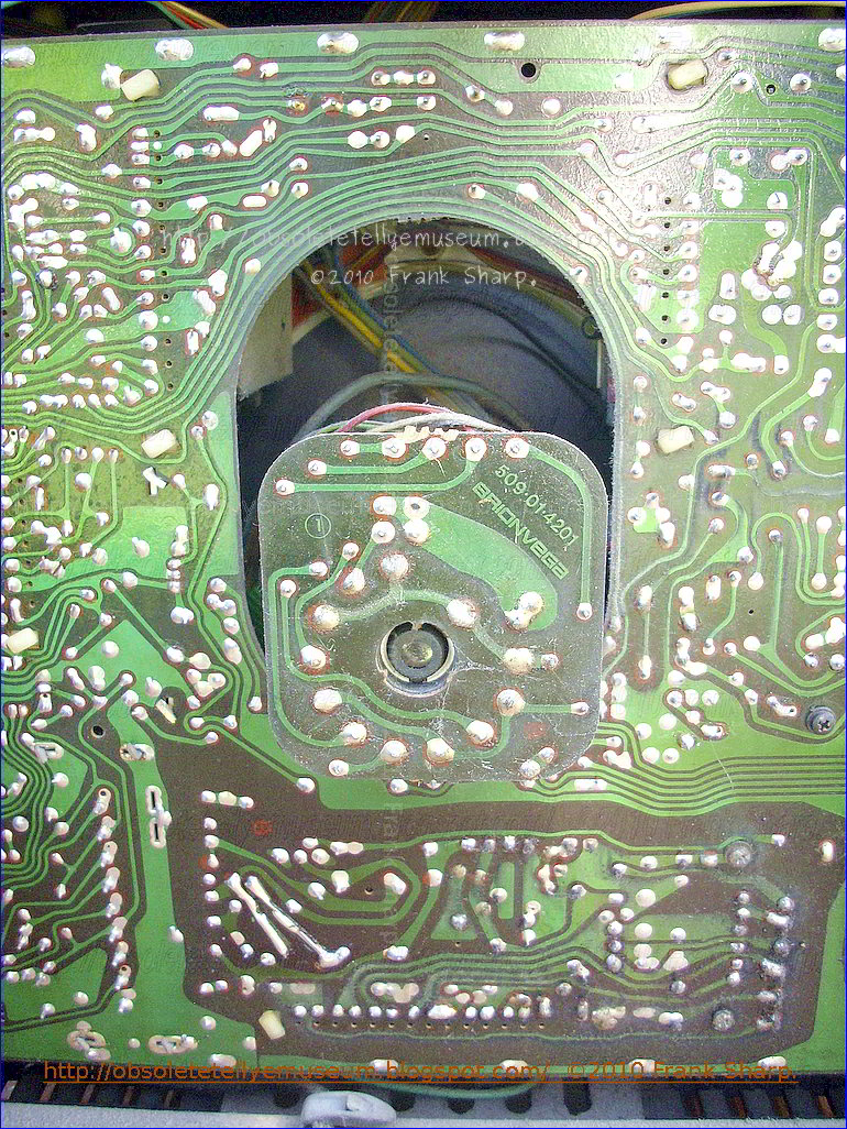
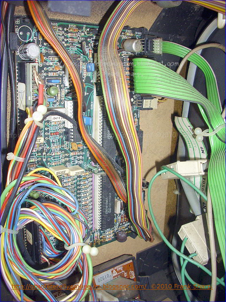
BRIONVEGA LED TVC 20 CHASSIS 509-01-3862
BRIONVEGA POWER SUPPLY CONTROL UNIT : 509-01-2931
BRIONVEGA SOUND UNIT 509-01-2081
BRIONVEGA E/W CORRECTION UNIT UNIT 509-01-2972
BRIONVEGA FRAME DEFLECTION OUT UNIT 509-01-29
BRIONVEGA SYNCHRONIZATION UNIT 509-01-3001 -3-
BRIONVEGA RGB AMPL. UNIT 509-01-3941
BRIONVEGA LUM. CHROM UNIT 509-01-4021
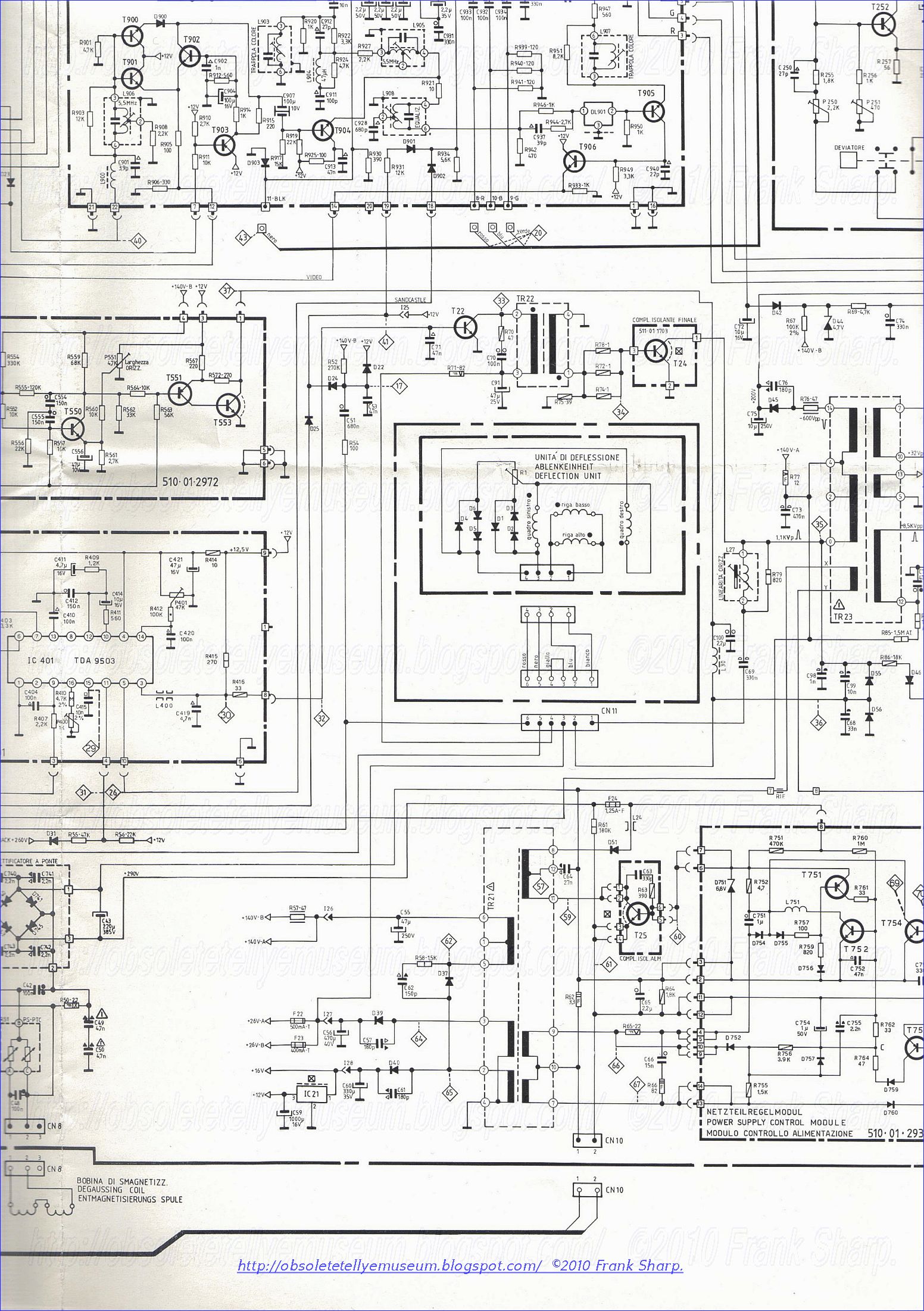
BRIONVEGA LED TVC 20 CHASSIS 509-01-3862 Synchronized switch-mode power supply:
The use of switching elements in electronic power supplies is well known in the present state of the art. The advantages of such power supplies include higher efficiency, lower weight and smaller size in comparison to analog power supplies. At some power levels, switching-mode power supplies are even less costly than their analog counterparts.
The size and weight advantages of switching-mode power supplies are achieved by operating their transformers and other magnetic components at high frequencies. In a conventional power supply, the transformer is operated directly from the main power source and, accordingly, is operated at the frequency of the power source.
The size advantages of commercial switching-mode power supplies result from the operation of the power transformers at a frequency well above that of standard power line frequencies. In fact, it is usually well into the high audio frequency or ultrasonic frequency range. Dramatic miniaturization is thus achieved, albeit at the expense of somewhat greater circuit complexity.
For the same power levels, a conventional transformer will vary in size approximately inversely with frequency. As frequencies become higher and higher, cores having suitable core loss characteristics cause the relationship to become less favorable since the so-called "low-loss" materials may have low maximum flux density capabilities. Thus, the core size itself will be larger than would be predicted if a change in core material was not required. Nonetheless, transformers having extraordinarily high volt-amp ratings per unit volume, are made possible by operation at the high frequencies possible with switching-mode circuitry.
Because the switching-mode power supply is lightweight and has such superior compactness, it has become more and more the design of choice for small, semi-portable equipment. In fact, the use of switching-mode supplies is now being seen in applications which were once thought to be the exclusive domain of analog supplies such as in small digital computers, in particular those intended for small business applications, where compactness is considered an important attribute for ease of installation in an office environment.
The conventional approach to design of switching-mode power supplies has been to employ a magnetically-coupled multivibrator which uses a pair of high-efficiency, solid-state switches, each alternately switching one-half of a center-tapped transformer primary to cause a square-wave having peak voltage equal to twice the center-tap voltage to appear across the entire primary. On alternate half-cycles, the primary current flows first in one side of the primary through the switch which is on, then through the other side of the primary and its associated switch, each for one-half of the period of the supplier basis operating frequency.
The search for cost-effective ways to achieve a regulated switching-mode power supply has led to the adoption in recent years of the blocking oscillator and its variants as the basic power converter design. Although somewhat touchy in terms of start-up and wide load-range operation, the blocking oscillator is a highly efficient circuit both in terms of its power processing efficiency and its parts cost. Instead of a pair of switching transistors and a series-pass transistor as required for a regulated conventional DC-DC converter, the blocking oscillator-based power supply requires but a single switching transistor which can be made to perform the functions of both chopping the unregulated direct current supplied to the input, and regulating the voltage produced at the output.
In addition to the reduction in parts count, the blocking oscillator-based power supply can be rendered in a design which does not require the switching transistors to see twice the input voltage, as does the standard DC-DC converter. Instead the power switch sees a theoretical maximum voltage of significantly less than twice the input voltage, depending upon the duty cycle which is chosen for its operation. Thus, operation of the supply directly from a 220 volt rectified main power source is possible, even using currently available semi-conductor devices
Known chopper converters of this type contain, generally connected in
series between the output terminals of a D.C. power supply source
(filtered rectifier), an electronic switch such as a switching
transistor operating in the saturated and cut off mode and an inductor
which includes the primary winding of a transformer in which at least
one secondary winding supplies the A.C. energy obtained by the chopping,
which is then rectified to provide the D.C. supply voltages with a
ground insulated from the mains. In most of the known chopper power
supplies, one can vary the output voltages by action on the cyclic
ratio, i.e. the length of the saturated (closed) state of the switch,
for example, by controlling periodically the transistor-chopper by means
of a monostable flip-flop of variable length as a function of a voltage
which may be picked up at the output of a rectifier fed by a secondary
winding of the transformer so as to form a regulation loop.
Chopper power supplies have frequently been used in television
receivers to eliminate the bulky and heavy mains supply transformer and
make possible a regulation of the D.C. power supply voltage for this
receiver. They have often been combined in particular at the output
stage of the horizontal sweep circuit which supplies them with a pulse
signal at the line frequency that can be used to control the chopping.
Various combinations of sweep circuits and chopper power supplies have
described, for example, in the French patents or patent applications
with publication Nos. 2.040.217, 2.060.495, 2.167.549, 2.232.147 or
2.269.257, in which the regulation is also done by means of the
variation in the cyclic ratio of the saturated and cut off states of the
chopper transistor which, in some cases, is also used as the active
element of the (final) output stage of the line sweep circuit or of the
feeder stage which controls this circuit.

In a switch mode power supply, a first switching
transistor is coupled to a primary winding of an isolation transformer.
A second switching transistor periodically applies a low impedance
across a second winding of the transformer that is coupled to an
oscillator for synchronizing the oscillator to the horizontal frequency.
A third winding of the transformer is coupled via a switching diode to a
capacitor of a control circuit for developing a DC control voltage in
the capacitor that varies in accordance with a supply voltage B+. The
control voltage is applied via the transformer to a pulse width
modulator that is responsive to the oscillator output signal for
producing a pulse-width modulated control signal. The control signal is
applied to a mains coupled chopper transistor for generating and
regulating the supply voltage B+ in accordance with the pulse width
modulation of the control signal.
Description:
The invention relates to switch-mode power supplies.
Some television receivers have signal terminals for
receiving, for example, external video input signals such as R, G and B
input signals, that are to be developed relative to the common conductor
of the receiver. Such signal terminals and the
receiver common conductor may be coupled to corresponding signal
terminals and common conductors of external devices, such as, for
example, a VCR or a teletext decoder.

To simplify the coupling of signals between the
external devices and the television receiver, the common conductors of
the receiver and of the external devices are connected together so that
all are at the same potential. The signal lines of each external device
are coupled to the corresponding signal terminals of the receiver. In
such an arrangement, the common conductor of each device, such as of the
television receiver, may be held "floating", or conductively isolated,
relative to the corresponding AC mains supply source that energizes the
device. When the common conductor is held floating, a user touching a
terminal that is at the potential of the common conductor will not
suffer an electrical shock.
Therefore, it may be desirable to isolate the common
conductor, or ground, of, for example, the television receiver from the
potentials of the terminals of the AC mains supply source that provide
power to the television receiver. Such isolation is typically achieved
by a transformer. The isolated common conductor is sometimes referred to
as a "cold" ground conductor.

In
a typical switch mode power supply (SMPS) of a television receiver the
AC mains supply voltage is coupled, for example, directly, and without
using transformer coupling, to a bridge rectifier. An unregulated direct
current (DC) input supply voltage is produced that is, for example,
referenced to a common conductor, referred to as "hot" ground, and that
is conductively isolated from the cold ground conductor. A pulse width
modulator controls the duty cycle of a chopper transistor switch that
applies the unregulated supply voltage across a primary winding of an
isolating flyback transformer. A flyback voltage at a frequency that is
determined by the modulator is developed at a secondary winding of the
transformer and is rectified to produce a DC output supply voltage such
as a voltage B+ that energizes a horizontal deflection circuit of the
television receiver. The primary winding of the flyback transformer is,
for example, conductively coupled to the hot ground conductor. The
secondary winding of the flyback transformer and voltage B+ may be
conductively isolated from the hot ground conductor by the hot-cold
barrier formed by the transformer.
It may be desirable to synchronize the operation of
the chopper transistor to horizontal scanning frequency for preventing
the occurrence of an objectionable visual pattern in an image displayed
in a display of the television receiver.
It may be further desirable to couple a horizontal
synchronizing signal that is referenced to the cold ground to the
pulse-width modulator that is referenced to the hot ground such that
isolation is maintained.

A synchronized switch mode power supply, embodying an
aspect of the invention, includes a transfromer having first and second
windings. A first switching arrangement is coupled to the first winding
for generating a first switching current in the first winding to
periodically energize the second winding. A source of a synchronizing
input signal at a frequency that is related to a deflection frequency is
provided. A second switching arrangement responsive to the input signal
and coupled to the second winding periodically applies a low impedance
across the energized second winding that by transformer action produces a
substantial increase in the first switching current. A periodic first
control signal is generated. The increase in the first switching current
is sensed to synchronize the first control signal to the input signal.
An output supply voltage is generated from an input supply voltage in
accordance with the first control signal.
 GENERAL BASIC TRANSISTOR LINE OUTPUT STAGE OPERATION:
The
basic essentials of a transistor line output stag e are shown in Fig.
1(a). They comprise: a line output transformer which provides the d.c.
feed to the line output transistor and serves mainly to generate the
high -voltage pulse from which the e.h.t. is derived, and also in
practice other supplies for various sections of the receiver; the line
output transistor and its parallel efficiency diode which form a
bidirectional switch; a tuning capacitor which resonates with the line
output transformer primary winding and the scan coils to determine the
flyback time; and the scan coils, with a series capacitor which provides
a d.c. block and also serves to provide slight integration of the
deflection current to compensate for the scan distortion that would
otherwise be present due to the use of flat screen, wide deflection
angle c.r.t.s. This basic circuit is widely used in small -screen
portable receivers with little elaboration - some use a pnp output
transistor however, with its collector connected to chassis.
e are shown in Fig.
1(a). They comprise: a line output transformer which provides the d.c.
feed to the line output transistor and serves mainly to generate the
high -voltage pulse from which the e.h.t. is derived, and also in
practice other supplies for various sections of the receiver; the line
output transistor and its parallel efficiency diode which form a
bidirectional switch; a tuning capacitor which resonates with the line
output transformer primary winding and the scan coils to determine the
flyback time; and the scan coils, with a series capacitor which provides
a d.c. block and also serves to provide slight integration of the
deflection current to compensate for the scan distortion that would
otherwise be present due to the use of flat screen, wide deflection
angle c.r.t.s. This basic circuit is widely used in small -screen
portable receivers with little elaboration - some use a pnp output
transistor however, with its collector connected to chassis.
Circuit Variations:
Variations
to the basic circuit commonly found include: transposition of the scan
coils and the correction capacitor; connection of the line output
transformer primary winding and its e.h.t. overwinding
in series; connection of the deflection components to a tap on the
transformer to obtain correct matching of the components and conditions
in the stage; use of a boost diode which operates in identical manner to
the arrangement used in valve line output stages, thereby increasing
the effective supply to the stage; omission of the efficiency diode
where the stage is operated from an h.t. line, the collector -base
junction of the line output transistor then providing the efficiency
diode action without, in doing so, producing scan distortion; addition
of inductors to provide linearity and width adjustment; use of a pair of
series -connected line output transistors in some large -screen colour
chassis; and in colour sets the addition of line convergence circuitry
which is normally connected in series between the line scan coils and
chassis. These variations on the basic circuit do not alter the basic
mode of operation however.
Resonance
The
most important fact to appreciate about the circuit is that when the
transistor and diode are cut off during the flyback period - when the
beam is being rapidly returned from the right-hand side of the screen to
the left-hand side the tuning capacitor together with the scan coils
and the primary winding of the line output transformer form a parallel
resonant circuit: the equivalent circuit is shown in Fig. 1(b). The line
output transformer primary winding and the tuning capacitor as drawn in
Fig. 1(a) may look like a series tuned circuit, but from the signal
point of view the end of the transformer primary winding connected to
the power supply is earthy, giving the equivalent arrangement shown in
Fig. 1(b).
The Flyback Period:
Since the operation of the
circuit depends mainly upon what happens during the line flyback period,
the simplest point at which to break into the scanning cycle is at the
end of the forward scan, i.e. with the beam deflected to the right-hand side of the screen, see Fig. 2. At
this point the line output transistor is suddenly switched off by the
squarewave drive applied to its base. Prior to this action a linearly
increasing current has been flowing in the line output transformer
primary winding and the scan coils, and as a result magnetic fields have
been built up around these components. When the transistor is switched
off these fields collapse, maintaining a flow of current which rapidly
decays to zero and returns the beam to the centre of the screen. This
flow of current charges the tuning capacitor, and the voltage at A rises
to a high positive value - of the order of 1- 2k V in large -screen
sets, 200V in the case of mains/battery portable sets. The e
beam deflected to the right-hand side of the screen, see Fig. 2. At
this point the line output transistor is suddenly switched off by the
squarewave drive applied to its base. Prior to this action a linearly
increasing current has been flowing in the line output transformer
primary winding and the scan coils, and as a result magnetic fields have
been built up around these components. When the transistor is switched
off these fields collapse, maintaining a flow of current which rapidly
decays to zero and returns the beam to the centre of the screen. This
flow of current charges the tuning capacitor, and the voltage at A rises
to a high positive value - of the order of 1- 2k V in large -screen
sets, 200V in the case of mains/battery portable sets. The e nergy
in the circuit is now stored in the tuning capacitor which next
discharges, reversing the flow of current in the circuit with the result
that the beam is rapidly deflected to the left-hand side of the screen -
see Fig. 3. When the tuning capacitor has discharged, the voltage at A
has fallen to zero and the circuit energy is once more stored in the
form of magnetic fields around the inductive components. One half -cycle
of oscillation has occurred, and the flyback is complete.
nergy
in the circuit is now stored in the tuning capacitor which next
discharges, reversing the flow of current in the circuit with the result
that the beam is rapidly deflected to the left-hand side of the screen -
see Fig. 3. When the tuning capacitor has discharged, the voltage at A
has fallen to zero and the circuit energy is once more stored in the
form of magnetic fields around the inductive components. One half -cycle
of oscillation has occurred, and the flyback is complete.
Energy Recovery:
First
Part of Forward Scan The circuit then tries to continue the cycle of
oscillation, i.e. the magnetic fields again collapse, maintaining a
current flow which this time would charge the tuning capacitor
negatively (upper plate). When the voltage at A reaches about -0.6V
however the efficiency diode becomes forward biased and switches on.
This damps the circuit, preventing further oscillation, but the magnetic
fields continue to collapse and in doing so produce a linearly decaying
current flow which provides the first part of the forward s can,
the beam returning towards the centre of the screen - see Fig. 4. The
diode shorts out the tuning capacitor but the scan correction capacitor
charges during this period, its right-hand plate becoming positive with
respect to its left-hand plate, i.e. point A. Completion of Forward Scan
When the current falls to zero, the diode will switch off. Shortly
before this state of affairs is reached however the transistor is
switched on. In practice this is usually about a third of the way
through the scan. The squarewave applied to its base drives it rapidly
to saturation, clamping the vol
can,
the beam returning towards the centre of the screen - see Fig. 4. The
diode shorts out the tuning capacitor but the scan correction capacitor
charges during this period, its right-hand plate becoming positive with
respect to its left-hand plate, i.e. point A. Completion of Forward Scan
When the current falls to zero, the diode will switch off. Shortly
before this state of affairs is reached however the transistor is
switched on. In practice this is usually about a third of the way
through the scan. The squarewave applied to its base drives it rapidly
to saturation, clamping the vol tage
at point A at a small positive value - the collector emitter saturation
voltage of the transistor. Current now flows via the transistor and the
primary winding of the line output transformer, the scan correction
capacitor discharges, and the resultant flow of current in the line scan
coils drives the beam to the right-hand side of the screen see Fig. 5.
tage
at point A at a small positive value - the collector emitter saturation
voltage of the transistor. Current now flows via the transistor and the
primary winding of the line output transformer, the scan correction
capacitor discharges, and the resultant flow of current in the line scan
coils drives the beam to the right-hand side of the screen see Fig. 5.
Efficiency:
The
transistor is then cut off again, to give the flyback, and the cycle of
events recurs. The efficiency of the circuit is high since there is
negligible resistance present. Energy is fed into the circuit in the
form of the magnetic fields that build up when the output transistor is
switched on. This action connects the line output transformer primary
winding across the supply, and as a result a linearly increasing current
flows through it. Since the width is
dependent on the supply voltage, this must be stabilised.
Harmonic Tuning:
There
is another oscillatory action in the circuit during the flyback period.
The considerable leakage inductance between the primary and the e.h.t.
windings of the line output transformer, and the appreciable self
-capacitance present, form a tuned circuit which is shocked into
oscillation by the flyback pulse. Unless this oscillation is controlled,
it will continue into and modulate the scan. The technique used to
overcome this effect is to tune the leakage inductance and the
associated capacitance to an odd harmonic of the line flyback
oscillation frequency. By doing this the oscillatory actions present at
the beginning of the scan cancel. Either third or fifth harmonic tuning
is used. Third harmonic tuning also has the effect of increasing the
amplitude of the e.h.t. pulse, and is generally used where a half -wave
e.h.t. rectifier is employed. Fifth harmonic tuning results in a
flat-topped e.h.t. pulse, giving improved e.h.t. regulation, and is
generally used where an e.h.t. tripler is employed to produce the e.h.t.
The tuning is mainly built into the line output transformer, though an
external variable inductance is commonly found in colour chassis so that
the tuning can be adjusted. With a following post I will go into the
subject of modern TV line timebases in greater detail with other models
and technology shown here at Obsolete Technology Tellye !
BU208(A)
Silicon NPN
npn transistors,pnp transistors,transistors
Category: NPN Transistor, Transistor
MHz: <1 MHz
Amps: 5A
Volts: 1500V
HIGH VOLTAGE CAPABILITY
JEDEC TO-3 METAL CASE.
DESCRIPTION
The BU208A, BU508A and BU508AFI are
manufactured using Multiepitaxial Mesa
technology for cost-effective high performance
and use a Hollow Emitter structure to enhance
switching speeds.
APPLICATIONS:
* HORIZONTAL DEFLECTION FOR COLOUR TV With 110° or even 90° degree of deflection angle.
ABSOLUTE MAXIMUM RATINGS
Symbol Parameter Value Unit
VCES Collector-Emit ter Voltage (VBE = 0) 1500 V
VCEO Collector-Emit ter Voltage (IB = 0) 700 V
VEBO Emitter-Base Voltage (IC = 0) 10 V
IC Collector Current 8 A
ICM Collector Peak Current (tp < 5 ms) 15 A
TO - 3 TO - 218 ISOWATT218
Ptot Total Dissipation at Tc = 25 oC 150 125 50 W
Tstg Storage Temperature -65 to 175 -65 to 150 -65 to 150 C
Tj Max. Operating Junction Temperature 175 150 150 °C
-----------------------------------------------------
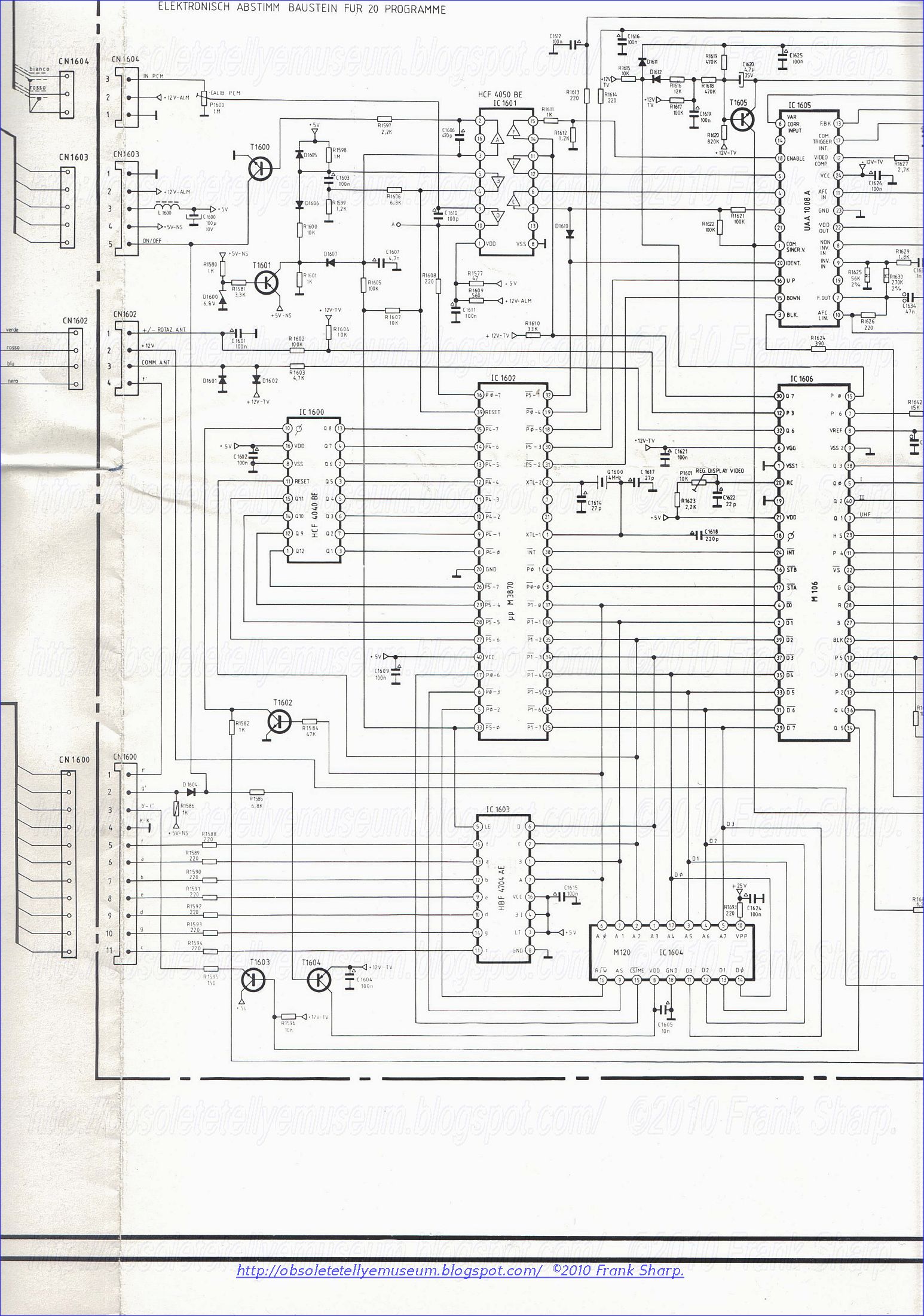
BRIONVEGA LED TVC 20 CHASSIS 509-01-3862 Frequency synthesizer tuning system for television receivers:
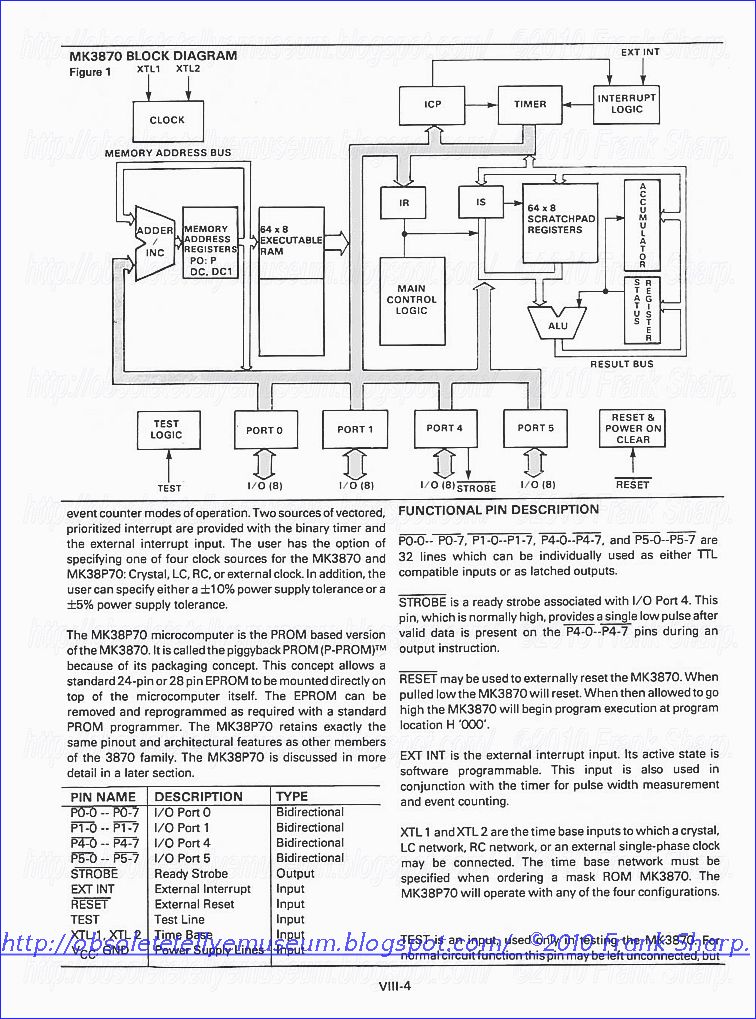
SHOWING M3870 Microcomputer + M206 PLL
"
A method for tuning a television receiver having automatic
frequency control to the carrier frequency of a selected broadcast
channel with an associated channel number including generating a
variable frequency signal by means of a local oscillator,
generating a reference frequency signal by means of a reference
oscillator, and generating a local oscillator correction signal for
matching an intermediate frequency signal derived from said local
oscillator signal and the carrier frequency signal with a
predetermined nominal intermediate frequency signal, said method
being characterized by the use of a microcomputer and comprising:
generating
binary signals representing first and second digital tune words,
said digital tune words representing a selected channel;
storing said first and second digital tune words in a first data memory in said microcomputer;
reading
said first and second digital tune words from said first memory
and generating a divided-down local oscillator frequency by the use
of said first digital tune word and a divided-down reference
oscillator frequency by the use of said second digital tune word;
comparing
said divided-down local oscillator and reference frequencies and
generating a control signal representative of the difference in
frequency of said divided-down local oscillator and reference
frequencies;
coupling said control signal to said local
oscillator for causing it to be locked to the frequency of said
received carrier signal;
mixing the local oscillator frequency signal and the carrier frequency signal to generate an intermediate frequency signal;
comparing
said intermediate frequency signal with said predetermined
nominal intermediate frequency signal and providing a tuning voltage
to said microcomputer, said tuning voltage being indicative of the
magnitude and direction of a tuning error between said
intermediate frequency signal and said predetermined nominal
intermediate frequency signal;
incrementally adjusting the
reference oscillator frequency by means of a tuning signal provided
to said reference oscillator by said microcomputer in response to
said tuning voltage;
detecting when the incrementally
changing, divided-down reference oscillator frequency causes the
intermediate frequency signal to pass said predetermined nominal
intermediate frequency signal; and
incrementally stepping the
divided-down reference oscillator frequency back a predetermined
number of steps following the passage of said predetermined nominal
intermediate frequency signal by said intermediate frequency
signal in tuning said television receiver to the selected channel.
"
PLL Synthesizer first time using a micro controller M3870 type With the
PLL synthesized tuning color television with frequency synthesized
tuning system, a television tuning system employs a frequency
synthesizer system for establishing the tuning of the receiver, featured
with a Microcomputer M3870 driven synthesis system. The 3870 Fairchild,
Motorola, SGS (SGS-Thomson)(MK3870) 8-bit microcontroller was a single
chip implementation of Fairchild F8 (Mostek 3850). The microcontroller
included up to 4 KB mask-programmable ROM, 64 bytes scratchpad RAM and
up to 64 bytes executable RAM. The MCU also integrated 32-bit I/O and
programmable timer. In addition to generic MK3870/xxx-xx markings the
3870 chips also had device order number in the form "MK#####x-xx".Mostek
also produced MK38P70 - development version of the 3870 MCU that
supported external EPROM chip. The system employed in the tv permits
utilization of a frequency synthesizer tuning system which correctly
tunes to a desired television station or channel even if the transmitted
signals from that station are not precisely maintained at the proper
frequencies even in combination of a fine tuning adjustable by the
user.The 3870, manufactured by Mostek, is a 3850 and 3856 on a single
chip.

A
television tuning system employs a frequency synthesizer system
for establishing the tuning of the receiver. A programmable
frequency divider counter is connected between the output of a
reference oscillator and a phase comparator to which the output of
the local oscillator in the tuner also is applied. The phase
comparator output provides a tuning voltage for controlling the
tuning of the local oscillator. A microprocessor is used to control
the count of the programmable frequency divider and initially to
set a count corresponding to the selected channel in a counter
connected between the output of the local oscillator and the phase
comparator. The tuning consists of three discrete time periods.
First, a settling time to allow channel change transients to
settle; second, a short period of forced search at a relatively
rapid rate to insure proper tuning; and third, a slower rate of
step-by-step correction to accomodate for station drift and the
like during reception. This third time period is initiated either
by the passage of a fixed length of time following the start of the
forced search period or by sensing a preestablished number of
changes of state in the output of the frequency discriminator during
the forced/search period.
1. A tuning
system for the tuner of a television receiver capable of receiving a
composite television signal and including frequency discriminator
(AFT) circuit means, said system including in combination:
a reference oscillator providing a reference signal at a predetermined frequency;
a
local oscillator in the tuner providing a variable output frequency
in response to the application of a control signal thereto;
a
programmable frequency divider means having first and second inputs
coupled respectively to the output of said reference oscillator
and said local oscillator for producing signals on first and second
outputs having frequencies which are a programmable fraction of the
frequency of the signals applied to the inputs thereto;

phase
comparator means having one input coupled with the first output of
said programmable frequency divider means and having another input
coupled with the second output of said programmable frequency
divider means for developing a control signal and applying such
control signal to said local oscillator for controlling the output
frequency thereof;
counter circuit means coupled with said
programmable frequency divider means for initially setting said
divider means to a predetermined division ratio and operating to
change the programmable fraction of division thereof in accordance
with changes in the count in said counter circuit means;
control
circuit means coupled with the output of said frequency
discriminator means and further coupled with said counter circuit
means for causing said counter circuit means to count at a first
rate in a predetermined direction determined by the state of the
output signal from said discriminator means in the absence of a
predetermined signal output from said frequency discriminator means
until a predetermined maximum count is attained, thereupon resetting
said counter circuit means to a count which is a predetermined
amount less than said maximum predetermined count and continuing to
count at said first rate in the same predetermined direction from
said new count to continuously change the programmable fraction of
said frequency divider means in accordance with the state of
operation of said counter circuit means, said control means
operating in response to said predetermined signal output from the
frequency discriminator means for terminating operation of said
counter circuit means; and
further means for terminating
operation of said counter circuit means at said first rate and
causing operation thereof at a second slower rate.
2. The
combination according to claim 1 wherein said further means includes
timing means initiated into operation simultaneously with the
setting of said divider means to a predetermined division ratio,
and after a predetermined time interval said timing means producing
an output signal applied to said counter circuit means to cause
operation thereof to take place at said second slower rate.
3. The combination according to claim
1 wherein said counter circuit means includes a reversible digital
counter coupled with said programmable frequency divider, means
and said control circuit means causes said counter circuit means to
count in said predetermined direction when the output of said
frequency discriminator is of a first state and to count in the
opposite direction when the output of said frequency discriminator is
of second state; and said further means comprises means coupled with
the output of said frequency discriminator and with said counter
circuit means to take place at said second slower rate in response
to a predetermined number of changes of state of frequency
discriminator. 4. The
combination according to claim 3 further including means responsive
to the selection of a new channel in said television receiver for
resetting said further means to an initial condition of operation.
5. The combination according
to claim 4 wherein said further means comprises a search
termination counter means operative to provide an output signal
applied to said counter circuit means in response to a count
thereby of a predetermined number of changes of state of said
frequency discriminator to cause said counter circuit means to be
operated at said second slower rate.
Description:
BACKGROUND OF THE INVENTION
Both of the above mentioned pat
ents
are directed to frequency synthesizer tuning systems for use with
television receivers to enable operation of the receivers with
minimal viewer fine tuning adjustments. By the utilization of the
frequency synthesizer tuning systems of these patents, the fine
tuning adjustment which is necessary with conventional types of
television receiver tuning systems has been substantially
eliminated. The system employed in the '953 patent permits utilization
of a frequency synthesizer tuning system which correctly tunes to a
desired television station or channel even if the transmitted
signals from that station are not precisely maintained at the
proper frequencies. The '535 patent is directed to a signal seek
tuning system adaptation of the frequency synthesizer tuning system
of the '953 patent which still permits implementation of all of
the desired wide-band pull in range of the frequency synthesizer
system of the '953 patent.
The systems of the foregoing
patents operate effectively to correct automatically for frequency
offsets in a frequency synthesizer tuning system without affecting
the operation of the conventional frequency synthesizer used in the
system. The systems of these patents are in widespread use
commercially and permit direct selection, with automatic fine
tuning adjustment, of any desired VHF channel which the viewer
wishes to observe. In addition, the signal seek adaptation disclosed
in the '535 patent couples all of the advantages of the frequency
synthesizer tuning system of the '953 patent with the desirability
of providing bidirectional signal seek operation.
While the
systems disclosed in the foregoing patents operate in a highly
satisfactory manner to accomplish the desired results of accurate
tuning without the necessity of fine tuning adjustments, the
circuitry for accomplishing the desired results is somewhat
complex. It is desirable to reduce the circuit complexity and the
number of signal detectors for accomplishing these results without
compromising the accuracy of operation of the system.
SUMMARY OF THE INVENTION
Accordingly, it is an object of this invention to provide an improved tuning system for a television receiver.
It
is an additional object of this invention to provide an improved
frequency synthesizer tuning system for a television receiver.
It
is another object of this invention to provide an improved
frequency synthesizer tuning system for a television receiver which
includes a provision for adjusting the synthesizer loop for
frequency offsets in the received signal with a minimum number of
signal detectors.
It
is a further object of this invention to tune the local RF
oscillator of a television receiver to the correct frequency for a
selected channel with a frequency synthesizer tuning system, and
automatically to change the reference frequency of the synthesizer
system, or adjust the count of a programmable divider that produces a
signal that divides the frequency of the local oscillator of the
tuner, if the AFT signal produced by the AFT frequency discriminator
of the receiver is outside a predetermined range corresponding to
correct tuning.
It is still another object of this invention
to provide an improved frequency synthesizer tuning system for a
television receiver which operates to adjust the synthesizer loop for
frequency offsets in the received signal over a relatively wide
pull in range in response to the output of the receiver frequency
discriminator by changing the division ratio of a programmable
frequency divider in the reference oscillator leg or local oscillator
leg of the synthesizer loop at a first relatively high rate from
an initial nominal value to a pre-established maximum in one
direction, and then resetting the division ratio to a second nominal
value once the maximum is reached and continuing to incrementally
change the division ratio in the same direction from the second
nominal value until a properly tuned condition is indicated by the
output of the receiver AFT frequency discriminator, followed by
control at a lower rate of operation to maintain tuning during
transmitting station drifts.
In accordance with a preferred
embodiment of this invention, the frequency synthesizer tuning
system for a television receiver includes a stable reference
oscillator and a voltage controlled local oscillator in the tuner. A
programmable frequency divider is connected between the output of
the reference oscillator and one input to a phase comparator, the
other input of which is supplied by the output of the local
oscillator. The output of the phase comparator then comprises a
control signal which is supplied to the local oscillator to control
the frequency of its operation.

A
counter circuit is connected to the programmable frequency divider
for initially setting the divider to a predetermined division
ratio upon selection of a desired channel by the viewer. The
counter then operates to change the programmable fraction of the
division ratio at a first relatively high rate in a direction
controlled by the output from the receiver picture carrier
discriminator in the absence of a predetermined signal output
derived from the discriminator. A control means causes the counter
circuit to count in this direction until it is determined that a
station is tuned or a predetermined maximum count is attained if no
station is correctly tuned, thereupon resetting the counter circuit
to a count which is a predetermined amount less than the maximum
predetermined count. Counting is continued in the same predetermined
direction from the new lesser count to continuously change the
programmable fraction of the frequency divider in accordance with
the state of operation of the counter.
The
high rate operation of the counter is terminated by the control
means in response to a predetermined signal from the output of the
discriminator, indicating that a station is correctly tuned, or after
a fixed time-out interval; so that the system automatically
adjusts for frequency offsets of the received signal which
otherwise would cause the station to be mistuned if a conventional
frequency synthesizer tuning system were used. After termination of
the high rate operation of the counter, it is switched to a lower
rate operation for maintaining tuning during transmitting station
drifts.
BRIEF DESCRIPTION OF THE DRAWINGS
FIG. 1 is a block diagram of a television receiver employing a preferred embodiment of the invention;
FIG. 2 is a detailed block diagram of a portion of the circuit of the preferred embodiment shown in FIG. 1;
FIG. 3 is a detailed circuit diagram of a portion of a circuit shown in FIG. 1;
FIG. 4 is a flow chart of the control sequence of operation of the circuit shown in FIG. 1 and 2; and
FIG.
5 shows a waveform and time/frequency chart, respectively, useful
in explaining the operation of the circuit shown in FIGS. 1, 2 and
3.
DETAILED DESCRIPTION
Referring now to the drawings,
the same reference numbers are used throughout the several figures
to designate the same or similar components.
FIG. 1 is a block diagram of a television receiver, which may be a black and white or color television receiver. Mo

st
of the circuitry of this receiver is conventional, and for that
reason it has not been shown in FIG. 1. Added to the conventional
television receiver circuitry of FIG. 1, however, is a frequency
synthesizer tuning system, in accordance with a preferred embodiment
of the invention, which is capable of automatically changing the
reference frequency when a frequency offset exists in the received
signal for a particular channel.
Transmitted composite
television signals, either received over the air or distributed by
means of a master antenna TV distribution system, are received by an
antenna 10 or on antenna input terminals to the receiver. As is
well known, these composite signals include picture and sound
carrier components and synchronizing signal components, with the
composite signal applied to an RF and tuner stage 11 of the
receiver. The stage 11 includes the conventional RF amplifiers and
tuner sections of the receiver, including a VHF oscillator section
and a UHF oscillator section. Preferably, the UHF and VHF
oscillators are voltage controlled oscillators, the freuency of
operation of which are varied in response to a tuning voltage
applied to them to effect the desired tuning of the receiver.
The
output of the RF and tuner stages 11 is applied to the remainder
of the television receiver 14, which includes the IF amplifier
stages for supplying conventional picture (video) and sound IF
signals to the video and sound processing stages of the receiver 14.
The circuitry of the receiver 14 may be of any conventional type
used to separate, amplify and otherwise process the signals for
application to a cathode ray tube 16 and to a loudspeaker 17 which
reproduce the picture and sound components, respectively, of the
received signal.
The receiver 14 also includes a conventional
AFT or automatic fine tuning discriminator circuit and
additionally may include a synch separator circ
uit
for producing an output in response to the presence of vertical
synchronizatin pulses, a picture carrier detection circuit, and an
automatic gain control (AGC) amplifier. Outputs representative of
these sensor components are shown as being coupled over a group of
lead 20 to sensory circuitry 22, which in turn couples outputs
representative of the operation of these various sensor circuits to
a microprocessor unit 23 for controlling the operation of the
microprocessor unit.
The microprocessor unit 23 is utilized
in the system of FIG. 1 for controlling the operation of a
frequency synthesizer tuning system capable of automatic offset
correction. When the viewer desires to select a new channel, he
enters the desired channel number into a channel selection keyboard
25. There are a number of different keyboards which may be employed
to accomplish this function, and the particular design is not
important to this invention. The channel selector keyboard 25 also
may include switches or keys for initiating a signal seek function
in either the "up" or "down" direction.
Information
represented by the selection of channel numbers on the keyboard 25 is
supplied to the microprocessor unit 23 which provides output
signals over a corresponding set of leads 27 to the tuners (local
oscillators) 11 to effect the appropriate band switching control for
the tuners 11 in accordance with the particular channel which has
been selected. In addition, the keyboard 25, operating through the
microprocessor unit 23, provides output signals which operate a
channel number display 29 to provide an appropriate display of the
selected channel number to the viewer.

The
microprocessor M3870 unit 23 also processes the signals which are
used to operate the channel number display 29 through a
multiplexing circuit operation to decode the selected channel
number into a parallel encoded signal. This signal is applied to
corresponding inputs of the count-down counter or programmable
frequency divider 31 to cause the division number of the divider 31
to relate to the divided down frequency of the tuner local
oscillators connected to the input of the divider 31 through a
prescaler divider circuit 32 to the frequency of the reference
oscillator 34. Thus, the division number or division ratio of the
local oscillator frequency obtained from the output of the
programmable divider 31 is appropriately related to the frequency of
the reference crystal oscillator 34.
The
output of the oscillator 34 also is applied through a countdown
circuit or programmable frequency divider 35. Conventional frequency
synthesizer techniques are employed; and the microprocessor unit 23
automatically compensates, through appropriate code converter
circuitry, for the non-uniform channel spacing of the television
signals. It has been found most convenient to cause the programmable
frequency divider 31 to divide by numbers corresponding directly to
the oscillator frequency of the selected channel, for example, 101,
107, 113 . . . up to 931.
In accordance with the time
division multiplex operation of the microprocessor 23, the count of
the programmable frequency divider 35 initially is adjusted to a
fixed count by the application of appropriate output signals from
the microprocessor unit 23 to a point selected to be at or near the
mid-point of the operating range of the programmable frequency
divider 35. Thus, the output of the divider 35 is a stable
reference frequency (because the input is from the reference
crystal oscillator 34) which is used to establish initially and to
maintain tuning of the receiver to the selected channel.
The
output of the programmable divider 35 is applied to one of two
inputs of a phase comparator circuit 37. The other input to the
phase comparator circuit 37 is supplied from the selected one of
the VHF or UHF oscillators in the tuner stages 11 through the
programmable frequency divider 31. The phase comparator circuit 37
operates in a conventional manner to supply a DC tuning control
signal through a phase locked loop filter circuit 39 and over a
lead 40 to the oscillators in the tuner system 11 to change and
maintain their operating frequency.
With the exception of the
use of the microprocessor unit 23, the operation of the system
which has been described thus far is that of a relatively
conventional frequency synthesizer system incorporated into a
television receiver. This system is similar to the system of the
'953 patent. As in the system of that patent, the system shown in
FIG. 1, when the transmitted station or station received on a
master antenna distribution system provides the station or channel
signals at the proper frequency, operates as a relatively
conventional frequency synthesizer system. If, however, there is a
frequency offset in the received signal to cause the carrier of the
received signal to be displaced from the frequency which it should
have to some other frequency, it is possible that the system would
give the appearance of mistuning to the received station. The
microprocessor 23, operating in conjunction with the sensory
circuitry 22, is employed in conjunction with the countdown or
programmable frequency divider circuit 35 to eliminate this
disadvantage and still retain the advantages of frequency
synthesizer tuning.
Reference now should be made to FIG. 2 which shows details of t

he
interface between the keyboard 25, the microprocessor unit 23, and
the circuitry used in the frequency synthesizer portions of the
system. A commercially available microprocessor which has been used
for the microprocessor 23, and which forms the basis for the
diagramatic representation of the microprocessor in FIG. 2, is the
Matsushita Electronics Corporation MN1402 four-bit single-chip
microcomputer. This microcomputer has two, four-bit parallel input
ports labeled "A" and "B". In addition, three output ports, a five-bit
output port "C" and two four-bit output ports "D" and "E" are
provided. The internal configuration of the microcomputer 23 includes
an arithmetic logic unit (ALU), a read only memory (ROM) for
storing instructions and constants, and a random access memory
(RAM) used for data memory, arranged into four files, each file
containing 16 four-bit words. These words are selected by X and Y
registers and this memory is used, for example, for timers,
counters, etc., and also is used to hold intermediate results. To
facilitate an understanding of the operation of the system, a
portion of this memory is shown in FIG. 2 as a clock 81 and a
reversible counter 82 connected between the "B" input port and the
"D" output port. The microcomputer 23 is programmed to permit it to
operate in conjunction with the remainder of the circuits shown in
FIG. 2. The programming techniques are standard, and the
microcomputer 23 itself is a standard commercially available
circuit component.
There are several system parameters that
must be selected in the operation of the system shown in FIG. 2.
The selection of the nominal frequency of the two signals that feed
the phase comparator circuit 37 is an example. Channel selection is
provided by changing the frequency division ratio of the selector
counter 31 which divides the local oscillator signal after this
signal is passed through a prescaler circuit 32 and a divide-by-two
divider circuit 41. The nominal frequency from the programmable
frequency divider 31 (selector counter) is selected so that the
local oscillator (tuner) 11 can be set exactly on frequency for all
channels.
Since
the frequency divider 31 is able to divide only by integer
numbers, one distinct frequency possibility in the range of one KHz
is obtained, another in the range of two KHz, etc. A choice must
be made as to which of these values is optimum. Each value yields
the nominal frequency of all of the 82 channels by simply
multiplying by an appropriate integer for each channel. To simplify
the phase locked loop filtering problem by the filter 39, it is
desirable that the frequencies of the signals supplied to the phase
comparator 37 are as high as possible. This permits rapid
acquisition of a new channel along with a very clean DC control
signal to adjust the local oscillator. A trade-off for this,
however, must be made to permit fine tunning adjustment of the local
oscillator automatically to correctly tune in stations which are
off their assigned frequency, or to manually provide this feature,
if desired. The two-speed operation of the system in accordance
with the present invention allows a better trade-off to be made by
allowing rapid acquisition and then a slower speed for precise
tuning.
A compromise solution which is utilized in the circuit
of FIG. 2 is to cause the frequency division chain from the local
oscillator 11 in the tuner to the phase comparator 37 to be composed
of the fixed divide-by-256 prescaler 32, and a fixed divide-by-4
division, which is accomplished by the divider 41 at the input of
the counter 31 and a second divider 42 at the output of the counter
31. The variable frequency divider counter 31 then is loaded by
means of three latch circuits 44, 45 and 46 at an appropriate time
by the time division multiplex operation of the microcomputer 23
and a number that programs the programmable frequency divider
counter 31 to divide by the numerical value of the frequency of the
local oscillator in MHz for the channel selected. For example, if
the receiver is to be tuned to channel 2, which has a nominal local
oscillator frequency of 101 MHz, the programmable frequency
divider 31 is set to divide by 101. If the receiver is to be tuned
to channel 83, which has a nominal local oscillator frequency of
931 MHz, the programmable frequency divider 31 is set to divide by
931. In both cases, the variable divider 31 produces a 1 MHz
signal. However, because of the fixed divide-by-256 and the two
fixed divide-by-two dividers in series with the programmable divider
31, an output frequency of 976.5625 Hz is supplied from the output
of the divider 42 to the upper input of the phase comparator 37.
The
division ratio of the selector counter 31 is established by
appropriate output signals from the latch circuits 44, 45 and 46, as
mentioned above. The initial operation for changing, or maintaining,
the division ratio of the divider 31 is established by an entry of
the two digits of the selected channel number in the keyboard 25.
The microcomputer 23 operates as a time division multiplex system
for continuously monitoring the input ports and the output ports to
control the operation of the remainder of the system. The selection
of the two digits of the desired channel number is affected by a
time division multiplex iscanning of the outputs of the D output
port of microcomputer 23 and providing that information at the A
input port.

From
here the information is translated again to the D output ports to
the appropriate drivers of the channel number display circuit 29 and
to the latches 44, 45 and 46, and to a pair of similar four bit
latches 49 and 50 which control the divider ratio of the counter 35.
Although
the D output ports of the microcomputer 23 are connected in common
to all of these various portions of the circuit, the selection of
which of the latches are enabled to respond to the particular
output signals appearing on the D output ports at any given time is
effected through the C and E output ports of the microcomputer 23
in a time division multiplex fashion. A decoder circuit 52,
connected to the lowermost three outputs of the E output port of
the microcomputer 23, is used to apply unique decoding signals at
different times in the tim
e
division multiplex sequence of operation of the microcomputer 23
to the five latch circuits 44, 45, 46, 49 and 50, respectively. At
any given time in the sequence, only one of these latch circuits is
enabled for operation. A latch load signal is applied from the
upper output (EO3) at each cycle of operation of the signals
appearing on the E output port to set the latch circuit which is
enabled by the output of the decoding circuit 52 with the data
appearing on the other inputs to the latch circuit. This data
simultaneously appears on the four outputs of the D output port of
the microcomputer 23.
Thus, in rapid sequence, the latch
circuits 44, 45 and 46 are set to store the division number
corresponding to the selected channel entered onto the keyboard 25,
and the latch circuits 49 and 50 are each operated to set the
programmable divider reference counter 35 to a center or nominal
count, which is always the same upon the selection of a new channel
on the keyboard 25. Similarly, the two right-hand outputs of the C
output port (CO6 and CO5) enter the two digits of the selected
channel number in the drivers of the display circuit 29 at the
proper time in the binary encoded sequence when these digits appear
on the four-bit binary encoded representation of the D output
port. This results in a visual display of the channel number
selected.
In addition to the selection of a channel number
directly by the keyboard 25, the keyboard also may include an
additional switch 56, which is scanned in the time division multiplex
sequence to determine if the receiver is placed in a "seek" mode
of operation (when the signal seek capability is incorporated into
such a receiver). Operating in conjunction with the signal seek
switch 56 are a pair of "up" and "down" seek direction input
switches shown with a graphic representation of the seek directions
on the keyboard 25. A further provision is provided by two keys
labeled "U" and "D", which are used for "manual" fine tuning of the
receiver in the "up" or "down" directions depending upon which of
the two keys U or D has been operated. The keyboard 25 includes one
additional switch 58 which may be used to disable the automatic fine
tuning (AFT) portion of the circuit by rendering the microcomputer
insensitive to the signal output from the AFT circuit, in a manner
described more fully subsequently.
As is apparent from the
foregoing, the microcomputer 23 provides the intelligence, decision
making, and control for the system operation. It is a complete self
contained computer. The decisions or signal inputs upon which the
microcomputer 23 bases its operation include, in addition to the
inputs from the keyboard 25, inputs on sensory inputs into the B
input port and into the SNS1 and SNS0 inputs as shown in FIG. 2.
These input signals are used to provide an indication to the
microcomputer 23 of the presence or absence of a received signal;
and if the presence of such a signal is indicated, the inputs
provide a further indication of the accuracy of the tuning of the
receiver to that signal. If the system is being operated solely in a
manual mode of operation (AFT switch 58 open), the microcomputer
23 disregards all of this sensory information and tunes to the
frequency allocation of the channel selected in the manner described
above. The system will stay tuned to this condition, operating as a
conventional frequency synthesizer, whether or not a station is
present in the received signal.
When
the system is placed in its automatic mode of operation (similar
to the mode of operation of the above mentioned '953 patent), the
counter 82, integrally formed as part of the microcomputer 23,
continuously adds or subtracts one number at a time from the nominal
value or programmable division fraction entered into the programmable
frequency divider 35 at the outset of each new channel number
selection when frequency offset (mistuning) is present. The counter
82 is driven at a relatively high counting rate by clock pulses from
the clock 81 during this initial or forced search mode of
operation. Thus, automatic offset correction is provided for any
channel which is off its assigned frequency. The offset correction
automatically adjusts the frequency of the local oscillator by
changing the division ratio of the signal from the reference
oscillator 35 applied to the lower input of the phase comparator 37.
By doing this, the output of the phase comparator 37 applied to
the local oscillator 11 varies to cause the oscillator to be tuned
in the proper direction to compensate for the transmitting station
mistuning.
When the system is operating in its automatic mode
of operation, the microcomputer 23 responds to the sensor
information applied to it on its B input ports and on the S1 input
port shown in FIG. 2. These inputs are obtained from the various
outputs of the operational amplifiers shown connected to the
corresponding input ports in the detailed circuit of FIG. 3.
Depending upon whether the receiver is provided with a signal seek
feature or not, one or more of the sensory inputs of the circuit of
FIG. 3 are used. The s

ystem
shown in the drawings has a capability of correcting for frequency
offsets larger than 1.5 MHz on channels 2 and 7 and approximately 2
MHz on channels 6 and 13. The remainder of the channels have a
range between these two values.
If the receiver is not tuned
properly, the micromputer 23 executes the localized search of the
tuning range mentioned above. Since there is a necessary settling
down time for the tuning of a television receiver immediately
following selection of a new channel, a time interval of 250
milliseconds has been selected to prevent any localized search or
offset frequency correction until the expiration of this "settling
down" time period. If, at the end of this 250 millisecond time
interval, a properly tuned station is present, this is indicated by
the sensory outputs from the television receiver and no localized
search is effected to change the division ratio or programmable
divider count in the reference counter 35 for a system that also
has signal seek.
A system with no signal seek capability is
described later that requires less sensory input but which uses a
time period where a forced search is required directly after the
settling time interval.
Upon
termination of the 250 millisecond settling down period, the
microcomputer 23 is rendered responsive to the sensory input signals on
its sensory input signal ports. In the simplest form, only the
output of the frequency discriminator 60 (FIG. 3) applied to three
comparators 61, 62 and 63 is used to provide the necessary tuning
information to the microcomputer 23. The outputs of these comparators
are applied to the B12 and B11 inputs of the microcomputer.
The
comparator 61 simply is a conventional comparator for determining
whether or not the output of the frequency discriminator is
positive or negative, as indicated in the upper waveform of FIG. 5.
The comparators 62 and 63 are each adjusted with appropriate
reference input levels to provide a narrow window centered about
the center tuning frequency (fc) of the receiver. If the tuning of
the receiver, as indicated by the output of the frequency
discriminator 60, is outside this window on either side of the
central axis shown in FIG. 5, one output condition is indicated on
the input terminal B11 of the microcomputer. Only when the tuning
frequency is within the tuning window, indicative of a properly
tuned receiver, is the appropriate input applied to the
microcomputer input terminal B11. This input overrides any other
input that may be present on the input terminal B12 and is
indicative of a properly tuned receiver. The input from the
frequency discriminator 60, as applied to the microcomputer on its
input port B12, is used to determine the direction of operation of
the counter 82 of the microcomputer for the localized search count
signals applied to the latch circuits 49 and 50 to change the count
of the reference programmable divider counter 35 on a step-by-step
basis.
The lower graph of FIG. 5 plots the relative frequency
of the local oscillator 11 to the received signal frequency with
respect to time. The various arrows are used to indicate the manner
of operation of the counter 82 in the microcomputer 23 in
conjunction with the reference counter 35 for adjusting for any
mistuning conditions which may exist after the initial station
selection has been effected in the manner described above.
If
the receiver is properly tuned, the outputs from the comparators 62
and 63 of FIG. 3 which are combined together and applied to the
input port B11 of the microcomputer 23, provide an indication that
the tuning is within the properly tuned center frequency window. As
a consequence, no further operation of the microcomputer to change
any of the outputs applied to the latch circuits 49 and 50 for the
duration of this condition is effected. On the other hand, if the
receiver is mistuned on either side of the proper tuning frequency,
the various operating characteristics shown in FIG. 5 are effected.
Assume
initially that the receiver is capable of making tuning
adjustments over a range of fc plus Δf to fc minus Δf, as indicated
in the top waveform of FIG. 5. Three specific examples of
mistuning will then be considered. Initially, assume that the local
oscillator is mistuned relative to the received signal to a
frequency f1 as shown in the lower graph of FIG. 5. In this
condition, the outout of the frequency discriminator 60 is positive
since this signal frequency lies to the lefthand side of the
center or properly tuned region of operation of the discriminator.
Under this condition of the operation, the input signal applied to
the sensor port B12 of the microcomputer 23 is such that the
microcomputer counter 82 is caused to advance in a positive
direction to change the programmable division ratio or count of the
reference counter 35 in a manner to force the output of the phase
comparator 37 to adjust the frequency of the local oscillator until
the proper tuning indicated at point B in the lower graph of FIG. 5
is reached. The time interval for accomplishing this result is
measured from the upper end of the arrow representative of the
frequency f1 to the point B.
Now assume that the receiver
mistuning is to a frequency f2 which as shown in FIG. 5 as located
on the righthand-side of the center axis fc. In this condition, the
discriminator output is negative. This is reflected in the output
of the comparator 61 applied to the input port B12 of the
microcomputer 23. The polarity of this sign
al
is identified by the microcomputer 23 to cause the counter 82 in
it to operate in the reverse direction. As this count is applied on
a step-by-step basis through the latch circuits 49 and 50 to the
reference counter 35, the division ratio or count of the reference
counter (divider) 35 is changed. As a result, the reference
oscillator signal applied to the phase comparator 37 causes the
phase comparator 37 output to drive the local oscillator frequency
in a direction opposite to that considered in the first example.
This is shown by the vector interconnecting the top of the arrow
representative of f2 to point A on the time/frequency graph of FIG.
5.
As discussed in the general discussion above, whenever the
tuning frequency reaches the narrow window on either side of fc, the
outputs of the comparators 62 and 63 provide the necessary
indication on the sensory input port terminal B11 to cause
termination of the operation of the counter 82 in the microcomputer
23. Then the reference counter 35 remains set to the count attained
just prior to the appearance of this input signal on the input port
B11 of the microcomputer 23.
A third mistuning condition can
exist, and ordinarily this condition results in an ambiguity which
cannot be corrected simply by responding to the signal polarity at
the output of the frequency discriminator. This is indicated by
the mistuned condition where the difference between the local
oscillator frequency f3 and the transmitter frequency is such that
the signal f3 lies in the range to the right of the negative
portion of the discriminator output shown in the upper waveform of
FIG. 5. In this condition, the associated sound causes the
discriminator output to be positive; so that the television
receiver normally would attempt to tune toward the next adjacent
channel and away from the properly tuned center frequency of the
channel which is desired. The output of the discriminator 60 in
this situation is the same as it was in th

e
first example considered for frequency f1; so that the counter 82
of the microprocessor 23 operates to change the count in the
reference counter 35 in a manner to cause the local oscillator
frequency to go higher toward a frequency f3 +Δf, as shown in FIG.
5.
A predetermined number of counts of the counter 82 in the
microcomputer 23 are necessary for the microcomputer to count
through the frequency range Δf, and this range is selected to be
within the pull in or operating range of the system. Once this count
has been attained, the microcomputer counter 82 immediately is
reset back to a count which corresponds to a frequency 2 Δf lower
than the frequency attained by the maximum count. This is indicated
in FIG. 5 by the frequency f3-Δf. Because the microcomputer counter
82 is limited to counting a number of counts equal to Δf, this new
frequency now is on the lefthand side of the center line fc, shown
in both waveforms of FIG. 5. This places the local oscillator
frequency at a point such that the frequency discriminator output is
the positive output shown on the lefthand-side of the upper
waveform of FIG. 5. Counting continues in the same direction as
previously. This time, however, it is in a proper direction to bring
about correct tuning; and when the center frequency is reached,
the output of the comparators 62 and 63 cause the microcomputer 23
to stop its count. The proper tuning point attained is indicated at
point C on the graph of the lower part of FIG. 5.
Because
the counter 82 of the microcomputer is limited to a maximum count
equivalent to Δf above its initial count and thereupon is reset to a
new count equivalent to 2 Δf lower than the maximum count, it is
not necessary to utilize any other sensory inputs in order to
properly tune the receiver over a wide pull in range (as much as
plus or minus 2 MHz). Only the output of the conventional frequency
discriminator 60 is used to provide the necessary sensory inputs.
The
counter 82 of the microcomputer 23 is operated by the clock 81
during the foregoing sequence of operation, immediately following the
selection of a new channel by the operation of the keyboard 25, at
a fast or high speed operation. Typically, the counter steps are
10 milliseconds per step; so that there are no initial visual
effects which can be noticed by an observer of the television
screen of the receiver being tuned. The maximum forced search
period is approximately 900 milliseconds in duration. At the end of
this time interval, a timer in the microcomputer 23 causes a
signal to be applied through the outputs of the E output port to
the decoder circuit 52 indicative of the completion of this time
interval. The decoder 52 then applies a pulse on an output lead
connected to the B13 input of the B input port of the microcomputer
23. This pulse is sensed by the microcomputer 23 and is applied to
the clock 81 to change the clock rate to a much slower rate,
approximately one-third (1/3) or one-fourth (1/4) the rate used
previously during the forced search mode of operation. This then
permits the system to accomodate station drifts which normally
occur at a very slow rate during the transmission and reception of a
television signal. As a consequence, it is possible to use more
filtering in the filter 39 on the tuning line (FIG. 1) and employ a
smaller frequency window for the channel verification sensed by
the circuitry shown in FIG. 3.
The
result is a more precise tuning from the receiver than is
otherwise possible if only a high speed operation of the clock 81
is utilized.
When the channel once again is changed by
operation of the keys in the keyboard 25 or operation of the
channel selection circuitry from a remote control unit, this new
channel input is sensed by the microcomputer 23 from the signals
applied to the A input port and the clock 81 is reset to its fast
time or the forced search mode of operation; and the process
resumes.
Instead of employing an additional decoding function
in the decoder 52, a separate decoder also could be connected to
the outputs of the D output ports to feed back the signal to the
B13 input terminal of the B input port of the microcomputer 23. The
operation of the system to change the rate or frequency of the
pulses applied by the clock 81 to the counter 82 otherwise is the
same as described above.
Although applicant has found that it
is preferable to correct for mistuning or frequency offsets by
adjusting the count or division ratio of the counter 35, such
offset adjustments also could be effected by adjusting the count in
the counter 31 in the local oscillator signal line. The operation in
such a case is the same as described above for adjusting the count
in the counter 35.
If the receiver is to be used with an
automatic signal seek mode of operation, however, additional sensory
inputs are necessary. These inputs operate in conjunction with the
output of the frequency discriminator 60. The operation of the
microcomputer 23 in controlling the count of the reference
programmable frequency counter divider 35 is the same as described
above. The additional sensory inputs simply are used in conjunction
with the outputs of the comparators 62 and 63 to signal the
microcomputer 23 to assure that tuning is to a picture channel
rather than an adjacent sound channel. This is accomplished by
utilizing the output of the synchronizing signal separator 65 which
is applied to a comparator 67 to produce an output signal to the
SNS1 sensory input of the microcomputer 23 only when vertical
synchronizing signal components are present.
In addition, the
output of a picture carrier detector 69 is applied to the input of a
comparator 70 to produce an output to the B10 sensory input of the
microcomputer 23. If the picture carrier detector 69 is producing
an output indicative of the presence of a carrier, but no output is
being obtained from the vertical synch separator 65 at the same
time, the system is mistuned to a sound carrier and the
microcomputer 23 is permitted to continue its localized search until a
properly tuned station is found. Only when there is coincidence of
signals from the picture carrier detector 69, the synch signal
separator 65, and the automatic frequency discriminator window as
determined by the comparators 62 and 63, is the microcomputer
operation terminated to indicate that a properly tuned channel is
present.
Further insurance of tuning the receiver only to a
strong signal also can be provided by the addition of an AGC
amplifier 72. This is connected to a comparator 74 coupled to the
B10 input port along with the output of the picture carrier
detector comparator 70. When the AGC amplifier 72 is used as a
sensory input, the microcomputer operation, when the system is used
in a signal seek mode, is only terminated to indicate reception of
a valid signal when that signal is strong enough to produce the
desired output from the comparator 74. The signal level which is
acceptable is set by a potentiometer 75.
It should be noted
that when the system is operated in a signal seek mode, the sensory
inputs must indicate the reception of a properly tuned signal
within a pre-established time period. If no signal is sensed by the
various sensory input circuits operating in conjunction with one
another as described above, the microcomputer 23 automatically steps
to the next channel number and repeats the sequence of operation
described above. This is when it is placed in its signal seek mode of
operation. If signal seek is not employed, the additional sensory
circuits 65, 69 and 72 are not necessary, and the inputs to the
microcomputer which are provided from these sensory circuits are not
utilized. The sensory signal input which is used both for a
receiver without a signal seek capability of operation and for a
receiver which has a signal seek mode of operation in it, is the
output of the frequency discriminator 60 operating in conjunction
with the comparators 61, 62 and 63 as described above.
As
indicated above, the wideband method of tuning precisely to an
incoming signal that is at the wrong frequency described here only
needs the frequency discriminator sensory information. The method
that uses the additional sensors described above is needed to make
this system operate compatibly with signal seek but it is not
restricted to seek operation.
For
a system that does not use signal seek operation, only the
frequency discriminator sensory input is required for proper
operation. The discriminator 60 is used for both fine tuning
direction information and to produce a frequency window to indicate
the presence of a correctly tuned station (channel verification).
Initially, after a channel change, there is a 250 millisecond
settling time, the same as the operation described above with
compatible seek. After that, however, comes a period of time where a
forced localized search is produced by the microcomputer 23. The
forced search is needed to insure that the system will correctly
tune to stations that initially may be tuned to the undesired zero
voltage crossover in the right half of the upper curve of FIG. 5.
Such signals may be within the frequency window of the discriminator
60; and if a search is not forced, this system will not correctly
tune. The compatible seek system described previously correctly
tunes the local oscillator without a forced search, because the
picture carrier detector and vertical detector do not give an output
for this situation and the system automatically goes into its search
mode of operation. However, the non-seek system does not have a
picture carrier sensor input and must be forced to search for an
initial period of time sufficient to allow the system to tune up to
its maximum frequency and then reset (loop) back to a frequency of 2
Δf lower. Then it is tuned to the positive left half portion of
the discriminator curve (FIG. 5) and the frequency window created
by the discriminator 60 is sufficient to insure proper tuning. If
the discriminator output produced by the desired incoming signal
created an initial situation that produces the correct tuning
direction information, i.e., in the left half of the curve of FIG.
5, or in the right half portion that gives the correct direction
and
frequency
window information, the forced search would not be needed.
However, the forced search will produce a correct tuning situation
anyway. In these cases, the tuning either is correct to begin with
or correct tuning is reached quickly. Then, even though the forced
search is active, it simply alternates up and down through the
correct tuning point because each time the receiver is tuned a little
high in frequency, it produces a negative output from the
discriminator 60; and the tuning direction signal causes the system
to tune down in frequency.
Then,
a positive discriminator output is produced, and the system tunes
up in frequency. This continues until the forced search is removed
by time-out of the microcomputer 23 (a fraction of a second). At
such time, the receiver is correctly tuned by the frequency window of
the discriminator to be very near fc. The system cannot tune to
the undesired discriminator crossover shown in the right half
portion of FIG. 5 because the polarity of the tuning direction
signal always causes it to tune away from that point.
The
fast time or forced search operation of the system can be
terminated in a different way other than the preestablished
time-out period described above in conjunction with the operation
of the circuit shown in FIG. 2. Generally, it is desirable to build
into the system (or program into the system by means of software)
such a maximum time-out period to effect the operation which has
been described above to terminate the search and cause the clock 81
thereafter to operate in a low speed mode of operation. Termination
also can be accomplished by sensing the number of changes in the
direction sensor input applied to the B12 terminal of the B input
port to cause the search to be terminated when this direction
changes three times (or more). By doing this, any flicker that
might be observed on the screen of the television receiver is
minimized, since the forced search still takes place at the high
rate of application of clock pulses from the clock 81 to the
counter 82 in the same manner described above.
Termination
of the search, however, also may be effected by means of a search
terminate counter 78 (FIG. 3), which is advanced by pulses applied
to it each time the output of the comparator 61 changes its sign
(indicative of a change in direction for the counter 82) as applied
to it through the B12 input port, as described earlier. After three
of these changes, or some other number if desired, an output pulse
is obtained from the search terminate counter 78 and is applied to
the SNS0 input of the microcomputer 23. This causes the operation
of the clock 81 to be switched to its low speed mode of operation
to terminate the fast or "forced search" mode of operation. The
next time a new channel number is entered on the keyboard 25, a
reset pulse is applied to the search terminate counter 78 to reset
it to its original or zero count, thereby readying it for another
sequence of operation. It is apparent that the search terminate
counter 78 may not always be operated to terminate the count, since
the time-out interval which is sensed by the decode circuit 52 and
applied to the B13 input port of the microcomputer 23 may occur
before there are three changes of direction of the search. In any
event, the next time a new channel number is entered into the
keyboard 25, the search terminate counter 78 is reset; so that it
is irrelevant whether this counter reaches a full count or not to
effect the termination of the forced search operation of the
system.
FIG. 4 shows the control sequence of the system which
is stored in the ROM (Read Only Memory) of the microcomputer 23.
The microcomputer 23 operates by always running through the flow
sequence, via loops L1, L2 and L3. Loop L1 corresponds to a new
channel selection by two digit number entry. Loop L2 corresponds to
channel number increment or decrement by an up or down key
operation, respectively, or by seek operation. Loop L3 corresponds
to fine tuning, either manual or automatic. To obtain exact timing for
system control, the microcomputer 23 receives a standard timing
pulse from the output of the reference counter 35 divided in a
divide-by-five counter 80 and applied to the A13 input port of the
microcomputer 23. The control functions which are programmed into
the microcomputer 23, as indicated in the flow chart of FIG. 4, are
outlined in the following paragraphs.
Channel Number
Correction: An invalid two digit channel number entry (0, 1, 84,
99) is corrected. When the operation of the receiver is in the
signal seek mode, the next channel up from 83 is channel 2, and the
next lower channel from channel 2 is 83.
PLL
Control I: For a given channel number, a corresponding binary code
for the PLL selector counter 31 is derived as described
previously. For UHF channels, the local oscillator frequency
separation between two adjacent channels is 6 MHz and the code for
PLL is generated by the microcomputer 23 through means of a simple
calculation. This code then is transferred from the microcomputer
23 to the latches 44, 45 and 46 as described previously.
PLL
Control II: This routine of the microcomputer 23 is used to
transfer the fine tuning data to the latches 49 and 50 which
control the count of the reference counter 35 in the PLL circuit.
Channel
Number Display: The channel number is transferred from the
microcomputer 23 to the driver latches of the display driver
circuit 29.
Key Input Detection: The keyboard is arranged as
the matrix circuit shown in FIG. 2. ROM programming for scanning
and acknowledging a keyboard entry only after successive
indications provides protection against false entry due to contact
bounce. The four data output lines of the D output port of the
microcomputer 23 are used to transfer data to the phase lock loop
section of the circuit and to the display circuit 29, as well as for
scanning the keyboard matrix circuit.
Time Count: The
microcomputer 23 receives a basic timing pulse of approximately 200 Hz
from the output of the divider 80 and performs various controls for
each timing pulse. By way of example, sensing for the vertical
synch input (when the system is used with a signal seek capability)
on the input port SNS1 takes place every 2.5 milliseconds.
Automatic seek timing is selected to be 133 milliseconds for UHF
channels. All of these timing pulses are derived from the basic
synchronization timing pulse applied to the microcomputer on the
A13 input port from the output of the divider 80. Various other
timing values used in the microcomputer to properly time multiplex
sequence the operation are derived from this basic timing pulse.
Sensor
Input Detection: As described previously, the output of the
comparators shown in FIG. 3 reflect the status of the tuning of the
television receiver. If no signal seek mode of operation is used,
only the frequency discriminator or AFT discriminator 60 is
necessary. When a system is being used in a signal seek mode, a
proper television signal receipt is indicated by the presence of a
vertical synch signal at the output of the synch signal separator
65 and corresponding outputs are applied to the input leads B10 and
B11 (high level input signals) indicative of tuning to the
"correct tuned" frequency discriminator window and reception of a
picture carrier. As stated previously, the signal present on the B12
input lead is used to determine the direction of tuning when the
receiver is operated in its automatic mode.
Mode Detection: The
status of the seek and automatic/manual (A/M) switches are
detected. If the A/M switch (not shown) is in its automatic
position, automatic seek and offset correction are active. If only
the seek switch is on, only seek is performed. If the A/M switch is
in manual, manual fine tuning (MFT) is active.
Automatic
Mode: If the TV receiver is not properly tuned for VHF channels in
automatic, the local oscillator frequency is shifted automatically
toward proper tuning. The fine tuning data is generated in the
microcomputer 23 and is transferred to the latches 49 and 50 for the
reference counter 35 in the PLL circuit.
Manual Fine Tuning
(MFT) Control: The local oscillator frequency is shifted by pushing
the fine tuning up (U) or down (D) pushbutton or switch. This MFT
control can be applied to VHF channels as well as to UHF channels.
Channel
Up/Down: When a channel up (upward pointing arrow) or down
(downward pointing arrow) key closure in the keyboard 25 is
detected, or upon a direct access to an unused channel, this routine
is activated and the system will advance to the next channel in
the selected direction.
The foregoing embodiment of the
invention which has been described above and which is illustrated in
the drawings is to be considered illustrative of the inventi
V
on,
which is not limited to the specific embodiment selected for this
purpose. For example, hard-wired logic could be used to achieve the
various circuit operations which are accomplished by the
microcomputer 23 in conjunction with the other portions of the
system. The relative ease of programming and debugging the
microcomputer 23, however, make it much simpler to implement the
system operation with the microcomputer than with hard-wired logic.
With respect to the sensor circuit inputs to the system, an added
degree of operating assurance can be provided by the addition of a
sound carrier sensor in addition to the picture carrier sensor shown
in FIG. 3. If this feature is desired, the output of the
comparator for the sound carrier is combined with the outputs of
the comparators 70 and 74 at the input terminal B10 of the B input
port of the microcomputer 23. Because of the manner of the circut
operation which has been described previously, however, the addition
of a sound carrier detector to the system is not considered
necessary, even for a system operating in the signal seek mode of
operation. This is in contrast to conventional television receivers
having a signal seek operation, in which detection of the sound
carrier generally is a necessity to insure that mistuning of the
receiver to an adjacent sound carrier does not take place.




M206 PLL TV MICROCOMPUTER INTERFACE:
HIGHLY
INTEGRATED SOLUTION INCLUDING PLL SYNTHESIZER, NV MEMORY, D/A
CONVERTERS, BAND SELECT OUTPUTS,CLOCK OSCILLATOR, IR SIGNAL PRE
PROCESSOR 32 x 16 BITS AND OF NV SERIAL MEMORY BUS INTERFACE WITH
LIFETIMES OF 104 CYCLES/WORD AND MINIMUM 10 YEARS RETENTION STORES
TUNING
- DATA FOR 30 CHANNELS PLUS PRESET VAL PRE-PROCESSOR UES FOR THE SIX ANALOG FOR OUTPUTS
- INFRARED REMOTE CONTROL SIGNALS REDUCES COMPONENT SIX PWMCOUNT
- D/A CONVERTERS WITH 64-STEP RESOLUTION
- FOUR OPEN-DRAIN BAND SELECT OUTPUTS ON-CHIP RATED 4 MHz TOCLOCK 13.2 V
- OSCILLATOR WITH INTEGRATED BUFFERED OUTPUT
- DIGITAL POWER-ON RESET 3-WIRE SERIAL BUS TO LOAD/READ INTERNAL REGISTERS.
The
M206 is a highly integrated, programmable LSI integrated circuit for
microcomputer controlled TV applications, realized using an advanced
N-channel double polysilicon gate technology (NVMOS) that allows the
integration of non-volatile memory and standard logic on the same chip.
It contains a phase-locked loop (PLL) synthesizer, six pulse-width
modulation (PWM) digital/analog converters, a four-bit parallel output
buffer, clock oscillator with buffered output, pre-processor for
infrared remote control signals and a 3-wire serial bus interface. The
M206 interfaces with a microcomputer through the three-wire serial bus
and is programmed by loading thirteen internal registers - twelve of
which are readable to simplify programming. The PLL synthesizer requires
an external 64 + 15/16 prescaler and divider and works with a phase
comparator reference frequency of 0.9765 kHz. Outputs are provided to
control the division ratio of the prescaler and to signal the
out-of-lock condition to the microcomputer.
The infrared remote
control signal pre-processor consists of a preamplifier, a squarer and a
digital filter to separate noise from signals transmitted by the M708,
M709 and M710 remote control transmitters. The output of this
pre-processor is con- nected to the interrupt input of a microcomputer
programmed to receive and decode the signal. The M206 is supplied with
two separate 5 V supply inputs, each provided with internal power-on
reset circuits. The first, VDD1, supplies the remote control and clock
circuits in both standby and TV set operation. The second, VDD2,
supplies the rest of the circuits and is only active during TV
operation. The M206 is packaged in a 28-pin dual in-line plastic
package.
To use the internal oscillator a 4MHz quartz crystal
is connected between the pins CLIN and CLOUT. If an external clock is
used this must be connected to CLIN and CLOUT left unconnectedor, if
required as a clock output, loaded by a capacitor up to 15pF. The
minimum external clock amplitude is 2V peak- to-peak. A buffered clock
output, CLBUF, is provided which can drive up to three ± 100μA loads.
Register Reading
M206
registers are read by transmitting a 15-bit word with R/W low and the
address of the register to be read in A0, A1, A2, A3. Bits D0-D7 can be
high or low except when register 9 is addressed. If this word is
received correctly the SBE line is immediately pulled low by the M206
and after 24μs the contents of the addressed register will be available
to be read (see Figure 4). The microprocessor reads this data by sending
eight clock pulses. Data is output on the low-high transition of SBC
and the first data bit is available before the first clock pulse.
Loading the Non-volatile Memory Data is stored in the 32 x 16-bit NV
memory by loading the new contents into registers 10 and 11 then the
address into register 9. The memory modify cycle begins when the address
has been loaded and successful completion is indicated by a logic ”1”
in bit zero of register 12. The time for a modify cycle varies from a
few milliseconds to several hundred milliseconds during the device
lifetime and is not internally limited. The storage operation should be
aborted after one second if it proves unsuccessful. This is done by
setting bit zero of register 12.
Reading the Non-volatile Memory
The
NV memory is read by loading the address into register 9. The contents
of the addressed word are automatically loaded into registers 10 and 11
and can be read by two register read operations. The data is ready 200μs
after the address load. PLL Counter The PLL counter consists of a
single counter that acts as the program counter (11-bit) and is swallow
counter (4-bit) alternately. Data for the PLL counter is loaded into
registers 6 and 7. Register 6 must be loaded first because the register 7
load operation initiates the data transfer to the PLL counter. The
reference frequency is produced by dividing the clock frequency by 4096.
With a 4MHz clock this gives a reference frequency of 976.5Hz. An
out-of-lock signal is generated (output OL) when the phase error between
the reference frequency and the input frequency exceed s 0.72 (2μs).
The phase comparator output, PCO, has a threestate push pull
configuration with a high level of 5V and a low level of 0V (with zero
current sink or pump). The output impedance (both states) is typically
200Ω (400Ω maximum). The phase compara- tor output can be set to a high
impedance state (both sink and pump transistors off) by setting bit 4 of
register 8. The output is held in the high impedance state until this
bit is reset. The phase comparatoroutput should be set to high impedance
when changing band.
Recovering Lock
The phase comparator
output can also be set to high and low levels to restore normal
operation when the oscillator stops or the prescaler functions
incorrectly at high frequency. In the first condition (oscillator off)
the prescaler sometimes oscillates, at high frequency. The loop reacts
by reducing the varicap voltage in an attempt to reduce the frequency,
thus worsening the situation. This out-of-lock condition is signalled to
the microprocessor (by the OL output) which can set the phase
comparator output to low level, forcing the varicap voltage up and
restarting the oscillator. The phase comparator output is forced low by
setting bit 5 of register 8. After about 1ms this bit is automatically
reset and the loop should lock again. When the out-of-lock condition is
caused by a failure of the prescaler to operate correctly at high
frequencies the loop reacts by increasing the voltage, hence the
frequency, again worsening the situation. To recover from this condition
the phase comparator output is set high. This is done by setting bit 6
of register 8 which, as in the previous case, resets itself after 1ms.
The out-of-lock condition could also be caused by unwanted changesin
band or PLL counter contents provoked by external interference (spikes
on supply etc.). For this reason it is always advisable to reload the
band and PLL counter registers before attempting to recover lock as
described above. If the phase comparator output is in the high impedance
state, the OL output signals the reset condition but not the
out-of-lock condition.
Digital/Analog Converters
The six
pulse-width modulation (PWM) D/A converters have a resolution of 64
steps and an output frequency of 16kHz (with 4MHz clock). At power on
reset they are set to a duty cycle of zero. Power On Reset The V DD1 and
VDD2 supplies have an integrated digital power on reset with a duration
of 250ms. The reset condition is signalled by a low level on the
out-of-lock output, OL. The microprocessor can test this condition by
reading bit 1 of register 12. This bit is zero during power on reset and
the OL output remains active until it is read. Reading this bit
automatically restores it to a high state. During power on reset time
commands from the micoprocessor are not acknowledged. Power on reset
also sets the phase comparator output to a high impedance, state. It is
restored by resetting bit 4 of register 8. Remote Control Signal
Pre-processor This section contains a preamplifier, squarer, digital
filter and a pulse generator.The digital filter enables the pulse
generator only if three successive nega- tive going pulses (4 edges) are
detected. The dis-tance between these pulses must be in the range
24-27μs (about 37-41kHz with a 4MHz clock). The input is not tested for
the duration of the output pulse (192-256μs). If this pre-processor is
used in conjunction with M709 or M710 remote control transmitters valid
signals can be recognized in the presence of extreme noise conditions.
Separating the signals from the noise externally in this way reduces the
number of interrupts that the microcomputer has to handle thus allowing
it to concentrate on other takes. To take advantage of this section the
M708, 709, 710 transmitters must operate with a clock frequency in the
range 492-508kHz. The input can be DC or AC compled to the I.R.
preamplifier. In case of DC coupling the quiescent input level is
suggested to be 1.5V.
ITT TDA9400/9500, Line Circuits for TV Receivers (18-Pin Plastic Package)
These integrated circuits are advanced versions of the well-known types TDA1940, TDA1940F, TDA1950 and TDA1950F are identical
TBA940/950,
TDA9400/9500 etc. integrated line oscillator circuits. except the
following: at pin 2 the types having the suffix "F" supply ,
They
comprise all stages for sync separation and line synchronisation
horizontal output pulses of longer duration compared with the basic I
in
TV receivers in one single silicon chip. Due to their high degree of
types Integration, the number of external components is very small.
This
integrated circuit contains the horizontal sweep generator (HO), the
amplitude filter (AS), the sync-signal separating circuit (SA) and
the frequency/phase comparator (FP). For the purpose of suppressing
noise pulses which are caused via the operating voltage during the
upper and the lower inversion point of the horizontal sweep generator
(HO) which contains a single capacitor (C) and a first threshold
stage circuit (SS1) with two fixed thresholds, there are provided a
second and a third threshold stage circuit (SS2, SS3), to the inputs
of which the sawtooth signal is applied, and with the thresholds
thereof, approximately 2 μs prior to reaching the upper or the lower
peak value of the sawtooth signal, are being passed through thereby.
The output signal of the second threshold circuit (SS2) and the
output signal of the third threshold stage circuit (SS3) which is
applied via the pulse shaper circuit (IF), are superimposed linearly
and, via the stopper circuit (blocking stage) (SP) serve to control
the application of the composite video signal (BAS) to the amplitude
filter (AS), or else they are applied to a clamping circuit which
serves to apply the operating points of the amplitude filter (AS)
and/or of the sync-signal separating circuit (SA) to such a potential
that these two stages, for the time duration of these output pulses,
are prevented from operating.
1. An integrated circuit for
color television receivers, comprising a voltage- or
current-controlled horizontal sweep generator (HO), an amplitude
filter (AS), a synchronizing-signal separating circuit (SA) and a
frequency/phase comparator (FP) which serves to synchronize the
horizontal sweep generator (HO), with said generator being a sawtooth
generator containing a single capacitor

(C) and a first threshold stage circuit (SS1) having two fixed thresholds, said integrated circuit further comprising:
a
second and a third threshold stage circuit (SS2, SS3) each being
supplied with the sawtooth signal on the input side, comprising each
time one threshold which, approximately 2μs prior to the reaching of
the upper or the lower peak value of the sawtooth signal, is being
passed thereby;
a pulse shaper circuit (IF) coupled to the
output of said third threshold stage circuit (SS3) which pulse shaper
circuit reduces the duration of the output pulse thereof to about the
duration of the output pulse of said second threshold stage circuit
(SS2), and
a stopper circuit (blocking stage) (SP) coupled to
the outputs of both said pulse shaper circuit (IF) and said second
threshold stage circuit (SS2), said stopper circuit having a signal
input to which there is applied a composite video signal (BAS) and a
signal output which is coupled to the input of said amplitude filter
(AS).
2. The invention of claim 1 wherein
the outputs of both said pulse shaper circuit (IF) and said second
threshold stage circuit (SS2) are coupled to a clamping circuit which
applies the operating points of said amplitude filter (AS) and said
sync-separating signal (SA) to such a potential that they are
prevented from operating.
3. An integrated horizontal sweep circuit comprising:
a generator for generating a sawtooth signal;
an amplitude filter having an input for receiving a composite video signal and having an output;
a sync-signal separating circuit having an input coupled to said amplitude filter output and having an output;
a frequency/phase comparator having a first input coupled to said separating circuit output,
a second input receiving said sawtooth signal and an output for controlling said generator; and
a
control circuit responsive to said sawtooth signal for inhibiting
said composite video signal when said sawtooth signal is within
predetermined signal level ranges about the upper and lower inversion
points of said sawtooth signal.
4. An integrated circuit in accordance with claim 3 wherein:
said
generator comprises a capacitor, circuit means for charging and
discharging said capacitor, and a first threshold circuit controlling
said circuit means in response to said sawtooth signal reaching a
first level corresponding to said first inversion point and a second
level corresponding to said second inversion point.
5. An integrated horizontal sweep circuit comprising:
a sawtooth signal generator;
an amplitude filter having an input receiving a composite video signal and having an output;
a sync-signal separating circuit having an input coupled to said amplitude filter output and having an output;
a
frequency/phase comparator having a first input coupled to said
separating circuit output, a second input receiving said sawtooth signal
and an output for controlling said generator; and
a control
circuit responsive to said sawtooth signal for inhibiting operation
of said amplitude filter and/or said sync-signal separating circuit
when said sawtooth signal is within predetermined signal level ranges
about the upper and lower inversion point of said sawtooth signal.
6. An integrated circuit in accordance with claim 5 wherein:
said
generator comprises a capacitor, circuit means for charging and
discharging said capacitor and a first threshold circuit controlling
said circuit means in response to said sawtooth signal reaching a first
level corresponding to said first inversion point and a second level
corresponding to said second inversion point.
Description:
BACKGROUND OF THE INVENTION
The
invention relates to an integrated circuit for (color) television
receivers, comprising a voltage- or current-controlled horizontal-sweep
generator, an amplitude filter, a synchronizing signal separating
circuit (sync-separator) and a frequency/phase comparator which serves
to synchronize the horizontal sweep generato
r which is a sawtooth
generator consisting of a single capacitor and of a first threshold
stage having two fixed switching thresholds, cf. preamble of the patent
claim. Such types of integrated circuits, for example, are known
from the technical journal "Elektronik aktuell", 1976, No. 2, pp. 7
to 14 where they are referred to as TDA 9400 and TDA 9500.
Especially
on account of the fact that the amplitude filter as well as the
horizontal sweep generator in the form of the aforementioned sawtooth
generator, are integrated on a single semiconductor body, it is likely
that noise interference pulses coming from the individual stages,
and via the supply voltage line, may have a disturbing influence upon
the horizontal sweep generator, i.e. upon the threshold stage
thereof, in such a way that either the lower or the upper or
successively both switching thresholds are exceeded before the time
by the voltage at the capacitor, owing to the noise superposition, so
that the generator will show to have a "wrong" frequency or phase
position. This frequency/phase variation, of course, is compensated
for by the circuit, with the aid of the synchronzing pulses, but only
in such a way that the noise effect remains visible in the
television picture.
SUMMARY OF THE INVENTION
The
invention is characterized in the claim is aimed at overcoming this
drawback by solving the problem of designing an integrated circuit of
the type described in greater detail hereinbefore, in such a way that
noise pulses acting upon the capacitor voltage or the internal
reference voltages for the switching thresholds (see below) in the
proximity of the two switching thresholds, are prevented from having
the described disadvantageous effect. Accordingly, an advantage of the
invention results directly from solving the given problem.
Other
objects, features and advantages of the present invention will
become more fully apparent from the following detailed description of
the preferred embodiment, the appended claims and the accompanying
drawing in which:
BRIEF DESCRIPTION OF THE INVENTION
The
invention will now be described in greater detail with reference to
the accompanying drawing. This drawing, in the form of a schematical
circuit diagram, shows the construction of an integrated circuit
according to the invention.
DETAILED DESCRIPTION OF THE INVENTION
The
horizontal sweep generator HO comprises the capacitor C as connected
to the zero point of the circuit, and which is charged and
discharged via the two shown constant current sources CS1 and CS2,
thus causing the intended sawtooth voltage to appear thereat.
Moreover, the horizontal sweep generator HO comprises the first
threshold stage circuit SS1, having an upper and a lower threshold.
As soon as the capacitor voltage exceeds one of the thresholds, the
first threshold stage circuit SS1 switches over to the other
threshold. The two thresholds are defined by the voltage divider P as
connected to the operating voltage U, and in which the corresponding
threshold inputs are connected to corresponding tapping points. The
output of the threshold stage circuit SS1 controls the electronic
switch S, so that the constant current source CS2 as connected
thereto, is either disconnected from or connected to the zero point
of the circuit. Accordingly, in the disconnected state, the capacitor
C is charged via the constant current source CS1 arranged in series
therewith while in the connected state the capacitor C is discharged
across the aforementioned constant current source CS2 arranged in
parallel therewith, if, as a matter of fact, the current of the
constant current source CS1 arranged in series with the capacitor C,
is smaller than that of the parallel-arranged constant current source
CS2.
Now, for the purpose of avoiding the aforementioned
drawbacks, there is provided a second and a third threshold stage
circuit SS2 and SS3, respectively, as well as the pulse shaper circuit
IF. To the respective input of the two threshold stage circuits SS2,
SS3, there is applied the capacitor voltage, in the form of the
sawtooth signal, and these stages have a threshold voltage which,
approximately 2 μs prior to the reaching of the upper or the lower
peak value of the sawtooth voltage, is being passed thereby. This
means to imply that the threshold voltage of the second threshold
stage circuit SS2 is somewhat lower than the voltage of the upper
threshold of the first threshold stage circuit SS1, and that the
threshold voltage of the third threshold stage circuit SS3 is
somewhat higher than the voltage of the lower threshold of the first
threshold stage circuit SS1. The two thresholds of the threshold
stage circuits SS2, SS3 can thus be realized in a simple way by
providing further tapping points at the voltage divider P, as is
shown in the accompanying drawing. Thus, the second threshold stage
circuit SS2 is provided for at a voltage divider tapping point below
the tapping point chosen for the upper threshold, and the tapping
point for the third threshold stage circuit SS3 is provided for above
the tapping point which has been chosen for the lower threshold of
the first threshold stage circuit SS1.
Since, within the area
of the lower inversion point of the sawtooth signal there results an
excessively wide output pulse of the third threshold stage circuit
SS3, the pulse shaper circuit IF is arranged subsequently thereto,
for reducing the duration of the output pulse as applied to its
input, to about the duration of the output pulse of the second
threshold stage circuit SS2. This pulse shaper circuit IF, for
example, may be realized by a monoflop, in particular by a digital
monoflop (=monostable circuit).
The output pulses of the
second threshold stage circuit SS2 and of the pulse shaper circuit IF
are then super-positioned linearly, with this being denoted in the
drawing by a simple interconnection of the two respective lines. The
combined signal is applied to the input of the stopper circuit
(blocking stage) SP, to the signal input of which there is fed the
composite video signal BAS, and the output thereof controls both the
amplitude filter AS and the synchronizing signal separating circuit
SA.
The combined signal may also be used to control a
clamping circuit applying the operating points of the amplitude filter
AS and/or of the sync-signal-separating circuit SA to such a
potential which prevents it from operating.
If now the
sawtooth signal reaches the range of its upper or its lower inversion
point, the composite video signal BAS is not applied to either the
amplitude filter AS or the sync-signal separating circuit SA, so that
shortly before and shortly after the inversion points, signals are
prevented from being processed in the two stages AS, SA. This, in turn,
has the consequence that during these times noise pulses are
prevented from superimposing upon the operating voltage U, so that
there is also prevented an unintended triggering of the first
threshold stage circuit SS1.
Moreover, it is still shown in
the drawing that the amplitude filter AS, the sync-signal separating
circuit SA and the frequency/phase comparator FP are arranged in
series in terms of signal flow, with the latter, in addition,
receiving the sawtooth signal, and with the output signal thereof
acting upon the two current sources in a regulating sense. In the
drawing, this is indicated by the setting arrows at the two current
sources.
While the present invention has been disclosed in
connection with the preferred embodiment thereof, it should be
understood that there may be other embodiments which fall within the
spirit and scope of the invention as defined by the claims.
The PHILIPS TDA3560A BRIONVEGA LED TVC 20 CHASSIS 509-01-3862
is a decoder for the PAL colour television standard. It combines all functions required for the identification
and demodulation of PAL signals. Furthermore it contains a luminance amplifier, an RGB-matrix and amplifier. These
amplifiers supply output signals up to 5 V peak-to-peak (picture information) enabling direct drive of the discrete output
stages. The circuit also contains separate inputs for data insertion, analogue as well as digital, which can be used for
text display systems (e.g. (Teletext/broadcast antiope), channel number display, etc. Additional to the TDA3560, the
circuit includes the following features:
· The peak white limiter is only active during the time that the 9,3 V level at the output is exceeded. The start of the
limiting function is delayed by one line period. This avoids peak white limiting by test patterns which have abrupt
transitions from colour to white signals.
· The brightness control is obtained by inserting a variable pulse in the luminance channel. Therefore the ratio of
brightness variation and signal amplitude at the three outputs will be identical and independent of the difference in gain
of the three channels. Thus discolouring due to adjustment of contrast and brightness is avoided.
 · Improved suppression of the internal RGB signals when the device is switched to external signals, and vice versa.
· Non-synchronized external RGB signals do not disturb the black level of the internal signals.
· Improved suppression of the residual 4,4 MHz signal in the RGB output stages.
· Cascoded stages in the demodulators and burst phase detector minimize the radiation of the colour demodulator
inputs.
· High current capability of the RGB outputs and the chrominance output.
APPLICATION INFORMATION
The function is described against the corresponding pin
number.
1. + 12 V power supply
The circuit gives good operation in a supply voltage range
between 8 and 13,2 V provided that the supply voltage for
the controls is equal to the supply voltage for the
TDA3561A. All signal and control levels have a linear
dependency on the supply voltage. The current taken by
the device at 12 V is typically 85 mA. It is linearly
dependent on the supply voltage.
2. Control voltage for identification
This pin requires a detection capacitor of about 330 nF for
correct operation. The voltages available under various
signal conditions are given in the specification.
3. Chrominance input
The chroma signal must be a.c.-coupled to the input.
Its amplitude must be between 55 mV and 1100 mV
peak-to-peak (25 mV to 500 mV peak-to-peak burst
signal). All figures for the chroma signals are based on a
colour bar signal with 75% saturation, that is the
burst-to-chroma ratio of the input signal is 1 : 2,25.
4. Reference voltage A.C.C. detector
This pin must be decoupled by a capacitor of about 330
nF. The voltage at this pin is 4,9 V.
5. Control voltage A.C.C.
The A.C.C. is obtained by synchronous detection of the
burst signal followed by a peak detector. A good noise
immunity is obtained in this way and an increase of the
colour for weak input signals is prevented. The
recommended capacitor value at this pin is 2,2 mF.
6. Saturation control
The saturation control range is in excess of 50 dB.
The control voltage range is 2 to 4 V. Saturation control is
a linear function of the control voltage.
When the colour killer is active, the saturation control
voltage is reduced to a low level if the resistance of the
external saturation control network is sufficiently high.
Then the chroma amplifier supplies no signal to the
demodulator. Colour switch-on can be delayed by proper
choice of the time constant for the saturation control
setting circuit.
When the saturation control pin is connected to the power
supply the colour killer circuit is overruled so that the colour
signal is visible on the screen. In this way it is possible to
adjust the oscillator frequency without using a frequency
counter (see also pins 25 and 26).
 7. Contrast control
The contrast control range is 20 dB for a control voltage
change from + 2 to + 4 V. Contrast control is a linear
function of the control voltage. The output signal is
suppressed when the control voltage is 1 V or less. If one
or more output signals surpasses the level of 9 V the peak
white limiter circuit becomes active and reduces the output
signals via the contrast control by discharging C2 via an
internal current sink.
8. Sandcastle and field blanking input
The output signals are blanked if the amplitude of the input
pulse is between 2 and 6,5 V. The burst gate and clamping
circuits are activated if the input pulse exceeds a level of
7,5 V.
The higher part of the sandcastle pulse should start just
after the sync pulse to prevent clamping of video signal on
the sync pulse. The width should be about 4 ms for proper
A.C.C. operation.
9. Video-data switching
The insertion circuit is activated by means of this input by
an input pulse between 1 V and 2 V. In that condition, the
internal RGB signals are switched off and the inserted
signals are supplied to the output amplifiers. If only normal
operation is wanted this pin should be connected to the
negative supply. The switching times are very short
(< 20 ns) to avoid coloured edges of the inserted signals
on the screen.
10. Luminance signal input
The input signal should have a peak-to-peak amplitude of
0,45 V (peak white to sync) to obtain a black-white output
signal to 5 V at nominal contrast. It must be a.c.-coupled to
the input by a capacitor of about 22 nF. The signal is
clamped at the input to an internal reference voltage.
A 1 kW luminance delay line can be applied because the
luminance input impedance is made very high.
Consequently the charging and discharging currents of the
coupling capacitor are very small and do not influence the
signal level at the input noticeably. Additionally the
coupling capacitor value may be small.
BRIONVEGA LED TVC 20 CHASSIS 509-01-3862 Video signal processing circuit for a color television receiver PHILIPS TDA3560: In a video signal processing circuit for a color television receiver, a
brightness setting, which is operative for external color signals as
well as for internal color signals and which does not produce a color
shift, can be obtained by combining with the luminance signal (Y) a
level shift signal (H) the amplitude of which is adjustable by the
brightness setting and by employing in each color channel two clamping
circuits, the first one of which clamps a first reference level (RL1)
in the external color signal (ER, EG, EB) onto a combination of the
level shift signal and the internal color signal (R, G, B) and the
second clamping circuit clamps a second reference leve (RL2)
which occurs in the sum signal of the internal and the external color
signal when the level shift signal has zero value, onto the cutoff level
of the relevant electron gun of a picture display tube.
1. A video signal
processing circuit for a color television receiver having inputs for a
luminance signal, for color difference signals and for external color
signals, comprising respective matrix circuits for combining the
respective color difference signals with the luminance signal to form
respective color signals, respective first clamping circuits for
clamping the respective external color signals onto the respective color
signals, respective combining circuits for combining the respective
clamped external color signals with the respective color signals,
respective second clamping circuits for clamping the outputs of the
respective combining circuits onto a predetermined level, and a
brightness setting circuit, characterized in that the first clamping
circuits act on a first reference level in said respective external
color signals occurring in a first group of periods and the second
clamping circuits act on a second reference level occurring in a second
group of periods which differ from the periods of the first group, while
the brightness setting circuit is an amplitude setting circuit for a
level shift signal, which is combined with the luminance signal prior to
processing the color difference signals, with which the relative
position of the second reference level with respect to the remaining
portion of the luminance signal is adjustable.
2. A video signal processing circuit as claimed in claim
1, characterized in that the respective first and second clamping
circuits are operative alternately and every other line flyback period.
Description:
BACKGROUND OF THE INVENTION
The invention
relates to a video signal processing circuit for a color television
receiver having inputs for a luminance signal, for color difference
signals, and for external color signals, comprising a matrix circuit for
combining a color difference signal with the luminance signal to form a
color signal, a first clamping circuit for clamping an external color
signal onto the corresponding color signal, a combining circuit for
combining a clamped external color signal with the corresponding color
signal, a second clamping circuit acting on an output signal of the
combining circuit and a brightness setting circuit.
A video
signal processing circuit of the type defined above is described in
Philip Data Handbook for Integrated Circuits, Part 2, May, 1980 as IC
TDA3560. The brightness setting, which is common for internal and
external video signals, is obtained by means of a common direct current
level setting of the second clamping circuits. The settings of the three
electron guns of a picture display tube coupled to the outputs of the
video signal processing circuit are changed to an equal extent by this
direct current level setting as a result whereof, due to the mutual
differences in the efficiency of the phosphors of the picture display
tube, a color shift may occur at a brightness adjustment. It is an
object of the invention to prevent this.
SUMMARY OF THE INVENTION
According
to the invention, a video signal processing circuit of the type defined
in the preamble is therefore characterized in that the first clamping
circuit acts on a first reference level occurring in a first group of
periods and the second clamping circuit acts on a second reference level
occurring in a second group of periods which differ from the periods of
the first group, while the brightness setting circuit is an amplitude
setting circuit for a level shift signal with which the relative
position of the second reference level with respect to the remaining
portion of the luminance signal is adjustable.
Owing to the
measure in accordance with the invention, the common setting of the
brightness for internal video signals is maintained and a color shift is
prevented from occurring at a brightness setting.
DESCRIPTION OF THE DRAWINGS
An embodiment of the invention will now be further described by way of example with reference to the accompanying drawings.
In the drawings:
FIG.
1 illustrates, by means of a block schematic circuit diagram, a video
signal processing circuit in accordance with the invention; and
FIG. 2 shows some waveforms such as they may occur in the circuit shown in FIG. 1.
DESCRIPTION OF THE PREFERRED EMBODIMENT

In
FIG. 1, an external red color signal ER' is applied to an input 1, a
red color difference signal (R-Y) to an input 3, an external green color
signal EG' to an input 5, a luminance signal Y to an input 7, a green
color difference signal (G-Y) to an input 9, an external blue color
signal EB' to an input 11, a blue color difference signal (B-Y) to an
input 13 and a synchronizing signal S to an input 15.
The
luminance signal at the input 7 is shown in FIG. 2 as a waveform 207. In
the line flyback periods this luminance signal has a black level Z
which, for simplicity, is assumed to occur in all cases during the whole
line flyback period but which may, of course, alternatively occur
during only a portion of that line flyback period.
The luminance
signal Y is applied to an input 17 of a combining circuit 19. To a
further input 21 thereof, a level shift signal H is applied which, via
an amplitude setting circuit 23, is obtained from an output 25 of a
pulse generator 27, to an input 29 of which the synchronizing signal S
is applied.
The level shift signal H is shown in FIG. 2 as a
waveform 221 which in this case has a zero amplitude every other line
flyback period and at other times an amplitude which depends on the
setting of the amplitude setting circuit 23.

The respective color
difference signals (R-Y), (G-Y) and (B-Y) at the respective inputs 3, 9
and 13, are applied to inputs 31, 33 and 35, respectively, of matrix
circuits 37, 39 and 41, respectively, to respective inputs 43, 45 and 47
of which the combination Y+H of the luminance signal (Y) and the level
shift signal (H) is applied, and from respective outputs 49, 51 and 53,
the red (R) and green (G) and blue (B) color signals are obtained. FIG. 2
shows the red color signal of said color signals as a waveform 249.
The
respective external color signals ER', EG' and EB' at the respective
inputs 1, 5 and 11 are applied to respective inputs 61, 63 and 65 of
respective combining circuits 67, 69 and 71 via respective capacitors
55, 57 and 59. Further inputs 73, 75 and 77, respectively, of the
combining circuits 67, 69 and 71, respectively, are connected to the
outputs 49, 51 and 53, respectively, of the matrix circuits 37, 39 and
41, respectively, and receive the red, green and blue color signals,
respectively.
Arranged between the inputs 61 and 73, 63 and 75,
and 65 and 77, respectively, there are first clamping circuits 79, 81
and 83, respectively, which, under the control of a pulse signal K
1 coming from an output 84 of the pulse generator 27, clamps a first reference level RL
1
in the respective external color signals ER', EG' and EB' onto the
respective color signals R, G and B, as a result of which the respective
clamped external color signals ER, EG and EB at the respective inputs
61, 63 and 65 of the combining circuits 67, 69 and 71 are produced, the
signal level ER at the input 61 of the combining circuit 67 being shown
in FIG. 2 as the waveform 261. The pulse signal K1 is shown in FIG. 2 as
the waveform 284.
At respective outputs 85, 87 and 89 of the
combining circuits 67, 69 and 71, respectively, there are now produced
signals which are the sums of the respective clamped external color
signals ER, EG and EB and the respective color signals R, G and B. Via
respective capacitors 91, 93 and 95, said sum signals (ER+R), (EG+G) and
(EB+B), respectively, are applied to respective inputs 97, 99 and 100
of respective video output amplifiers 102, 104 and 106, respective
outputs 108, 110 and 112 of which being connected to respective cathodes
of a picture display tube 114.
Second clamping circuits 116, 118
and 120, respectively, which are rendered operative by a pulse signal
K2 coming from an output 122 of the pulse generator 27 and whereby a
second reference level RL2 in the signals at the respective inputs 97,
99 and 100 is adjusted to a fixed potential, zero potential here, are
connected to the respective inputs 97, 99 and 100 of the respective
video output amplifiers 102, 104 and 106. This is shown in FIG. 2 by
means of the waveform 297 for the signal (ER+R) at the input 97 of the
video output amplifier 102. For the sake of clearness, the luminance
signal (Y) and the red color difference signal (R-Y) are assumed to have
zero values.
The picture display tube 114 has a deflection
circuit 124 which is controlled by signals coming from outputs 126 and
128, respectively, of the pulse generator 27.
On the basis of
FIG. 2, it will now be demonstrated that the brightness of the color
signals as well as of the external color signals is adjustable by means
of the amplitude setting circuit 23, more specifically in such a ratio,
occurring at the picture display tube 114, that no color shift is
produced.
If a luminance signal Y and a color difference signal
(R-Y) are produced and the external color signal ER' has zero value, the
signal at the output 49 of the matrix circuit 37 has the waveform 249
and likewise the signal at the input 97 of the video output amplifier
108, as during the occurrence of the signal K2 (waveform 222), the
second clamping circuit 116 has adjusted the second reference level RL
2
to zero, which corresponds to the cutoff level of the relevant cathode
of the picture display tube 114. Outside the periods in which signal is
clamped to the second reference level RL
2, the black level,
shown in the waveform 249 by means of a dashed line, of the color signal
at the input 97 of the video amplifier is determined by the amplitude
of the level shift signal H, which, in response to the video output
amplifier gain factors which are adapted to the efficiencies of the
phosphors of the picture display tube, are applied in the relevant
signal paths to the cathodes of the picture display tube 114 to said
cathodes in such an amplitude ratio that no color shift can be produced.
If there is an external color signal but no luminance and color
difference signals (Y=O, R-Y=O, G-Y=O, B-Y=O), then a signal is produced
at the input 97 of the video output amplifier 102 which has the
waveform 297 and which, during the occurrence of the second reference
level RL
2, is clamped onto zero by the second clamping
circuit 116 by means of the clamping pulses K2 and which consequently
corresponds to the cutoff level of the relevant cathode of the picture
display tube 114. During the occurrence of the first reference level RL
1
in the signal ER', the first clamping circuit 79 clamps the signal ER
(waveform 261) at the input 61 of the combining circit 61 onto the
output signal of the matrix circuit 37 during the occurrence of the
clamping pulses K1 (waveform 284). Now this output signal has the
waveform 221, as R-Y and Y have zero values. From the waveform 297, it
now appears that the signal ER+R, which in this case is equal to ER+H,
has, outside the periods in which the second reference level RL
2
occurs in the waveform 297, a black level which is indicated by means
of a dashed line and is determined by the amplitude of the level shift
signal H. Also now this amplitude is applied in the proper ratio to the
cathodes of the picture display tube 114 by the video output amplifier
gain factors which are adapted to the efficiencies of the phosphors of
the picture display tube 114, so that no color shift can be produced.
It
will be obvious that it is not imperative that the clamping pulses K1
and K2 be produced alternately and every other line flyback period. If
so desired, the clamping pulses K1 may, for example, occur in a number
of line trace periods of the field trace which are located outside the
visible picture plane, and the clamping pulses K2 may occur in the line
flyback periods. The clamping pulses K2 must be produced in the period
in which the level shift signal causes the second reference level RL
2 and the clamping pulses K1 outside said periods and in the periods the first level reference level RL
1 occurs.
In
the above-described embodiment the clamping circuits are provided in
the form of short-circuiting switches which are arranged subsequent to
capacitors which have for their function to block direct current
signals. It will be obvious, that, if so desired, clamping circuits in
the form of control circuits may alternatively be used and that in that
event, if so desired, blocking the direct current component by a
capacitor may be omitted.
If so desired, instead of an adder
circuit 19, an insertion circuit may be employed by means of which, in
the appropriate periods of the luminance signal, when the signal K2 is
produced the reference level Z then present, is replaced by a new level
which is influencable by the brightness setting .
TDA2541 IF AMPLIFIER WITH DEMODULATOR AND AFC
DESCRIPTION
The TDA2540 and 2541 are IF amplifier and A.M.
demodulator circuits for colour and black and white
television receiversusingPNPorNPNtuners. They
are intended for reception of negative or positive
modulation CCIR standard.
They
incorporate the following functions : .Gain controlled amplifier
.Synchronous demodulator .White spot inverter .Video preamplifier with
noise protection .Switchable AFC .AGC with noise gating .Tuner AGC
output (NPN tuner for 2540)-(PNP
tuner for 2541) .VCR switch for video output inhibition (VCR
play back).
East-west correction circuit relates to a deflection circuit i n which the amplitude of the deflection
current may be varied or modulated over a relatively wide range without
substantially affecting the high voltage amplitude or the deflection
retrace time. Modulation of the deflection current amplitude is desired
for such purposes as east-west pincushion distortion correction and
picture width adjustment.
n which the amplitude of the deflection
current may be varied or modulated over a relatively wide range without
substantially affecting the high voltage amplitude or the deflection
retrace time. Modulation of the deflection current amplitude is desired
for such purposes as east-west pincushion distortion correction and
picture width adjustment.
East-west pincushion distortion correction is accomplished in the
Haferl patent by supplying modulation current from a modulation current
source that varies at a vertical rate, through the decoupling inductive
impedance. During the retrace interval, the amount of energy supplied to
the retrace resonant circuit is directly related to the modulation
current provided by the modulation source. Therefore, the peak current
flowing in the deflection winding at the beginning of trace time, for
example, is also made to vary at a vertical rate, in a parabolic manner,
to achieve east-west pincushion distortion correction.
Testing Flyback Transformer
Nowadays, more and more monitor comes in with flyback transformers problems.
Testing flyback transformer are not difficult if you carefully follow the
instruction. In many cases, the flyback transformer can become short
circuit after using not more than 2 years. This is partly due to bad design
and low quality materials used during manufactures flyback transformer.
The question is what kind of problems can be found in a flyback transformer
and how to test and when to replace it. Here is an explanation that will help
you to identify many flyback transformer problems.
There are nine common problems can be found in a flyback transformer.
a) A shorted turned in the primary winding.
b) An open or shorted internal capacitor in secondary section.
c) Flyback Transformer becomes bulged or cracked.
d) External arcing to ground.
e) Internal arcing between windings.
f) Shorted internal high voltage diode in secondary winding.
g) Breakdown in focus / screen voltage divider causing blur display.
h) Flyback Transformer breakdown at full operating voltage (breakdown when under load).
i) Short circuit between primary and secondary winding.
Testing flyback transformer will be base on (a) and (b) since problem
(c) is visible while problem (d) and (e) can be detected by hearing the arcing
sound generated by the flyback transformer. Problem (f) can be checked with multimeter
set to the highest range measured from anode to ABL pin while (g) can be solved by
adding a new monitor blur buster (For 14' & 15' monitor only.) Problem (h) can only be
tested by substituting a known good similar Flyback Transformer. Different monitor have
different type of flyback transformer design. Problem (i) can be checked using an
ohm meter measuring between primary and secondary winding. A shorted turned or open
in secondary winding is very uncommon.
What type of symptoms will appear if there is a shorted turned in primary winding?
a) No display (No high voltage).
b) Power blink.
c) B+ voltage drop.
d) Horizontal output transistor will get very hot and later become shorted.
e) Along B+ line components will spoilt. Example:- secondary diode UF5404 and B+ FET IRF630.
f) Sometimes it will cause the power section to blow.
What type of symptoms will appear if a capacitor is open or shorted in a flyback transformer?
Capacitor shorted
a. No display (No high voltage).
b. B+ voltage drop.
c. Secondary diode (UF5404) will burned or shorted.
d. Horizontal output transistor will get shorted.
e. Power blink.
f. Sometimes power section will blow, for example: Raffles 15 inch monitor.
g. Power section shut down for example: Compaq V55, Samtron 4bi monitor.
h. Sometimes the automatic brightness limiter (ABL) circuitry components will get burned.
This circuit is usually located beside the flyback transformer. For example: LG520si
Capacitor open
a. High voltage shut down.
b. Monitor will have ‘tic - tic’ sound. Sometimes the capacitor may measure O.K. but
break down when under full operating voltage.
c. Horizontal output transistor will blow in a few hours or days after you have replaced it.
d. Sometimes it will cause intermittent "no display".
e. Distorted display i.e., the display will go in and out.
f. It will cause horizontal output transistor to become shorted and blow the power section.
How to check if a primary winding is good or bad in a Flyback Transformer?
a) By using a flyback/LOPT tester, this instrument identifies faults in primary winding by
doing a ‘ring’ test.
b) It can test the winding even with only one shorted turned.
c) This meter is handy and easy to use.
d) Just simply connect the probe to primary winding.
e) The readout is a clear ‘bar graph’ display which show you if the flyback transformer
primary winding is good or shorted.
f) The LOPT Tester also can be used to check the CRT YOKE coil, B+ coil and switch mode power transformer winding.
NOTE: Measuring the resistance winding of a flyback transformer, yoke coil, B+ coil and
SMPS winding using a multimeter can MISLEAD a technician into believing that a shorted
winding is good. This can waste his precious time and time is money.
How to diagnose if the internal capacitor is open or shorted?
By
using a normal analog multimeter and a digital capacitance meter. A
good capacitor have the range from 1.5 nanofarad to 3 nanofarad.*
1) First set your multimeter to X10K range.
2) Place your probe to anode and cold ground.
3) You must remove the anode cap in order to get a precise reading.
4) Cold ground means the monitor chassis ground.
5) If the needle of the multimeter shows a low ohms reading, this mean the internal capacitor
is shorted.
6) If the needle does not move at all, this doesn’t mean that the capacitor is O.K.
7) You have to confirm this by using a digital capacitance meter which you can easily get one
from local distributor.
8) If the reading from the digital capacitance meter shows 2.7nf, this mean the capacitor is
within range (O.K.).
9) And if the reading showed 0.3nf, this mean the capacitor is open.
10) You have three options if the capacitor is open or shorted.
- Install a new flyback transformer or
- Send the flyback transformer for refurbishing or
- Send the monitor back to customers after spending many hours and much effort on it.
* However certain monitors may have the value of 4.5nf, 6nf and 7.2nf.
Note: Sometimes the internal capacitor pin is connected to circuits (feedback) instead of ground.
Tv rca flyback transformer circuits usually do not have a internal capacitor in it.
If
you have a flyback diagram and circuits which you can get it from the
net, that would be an advantage to easily understand how to check them.
BRIONVEGA 523-99-0551 HR DIEMEN TV FLYBACK TRAFO---> HR3610


 External links
 Media related to Brionvega at Wikimedia Commons