

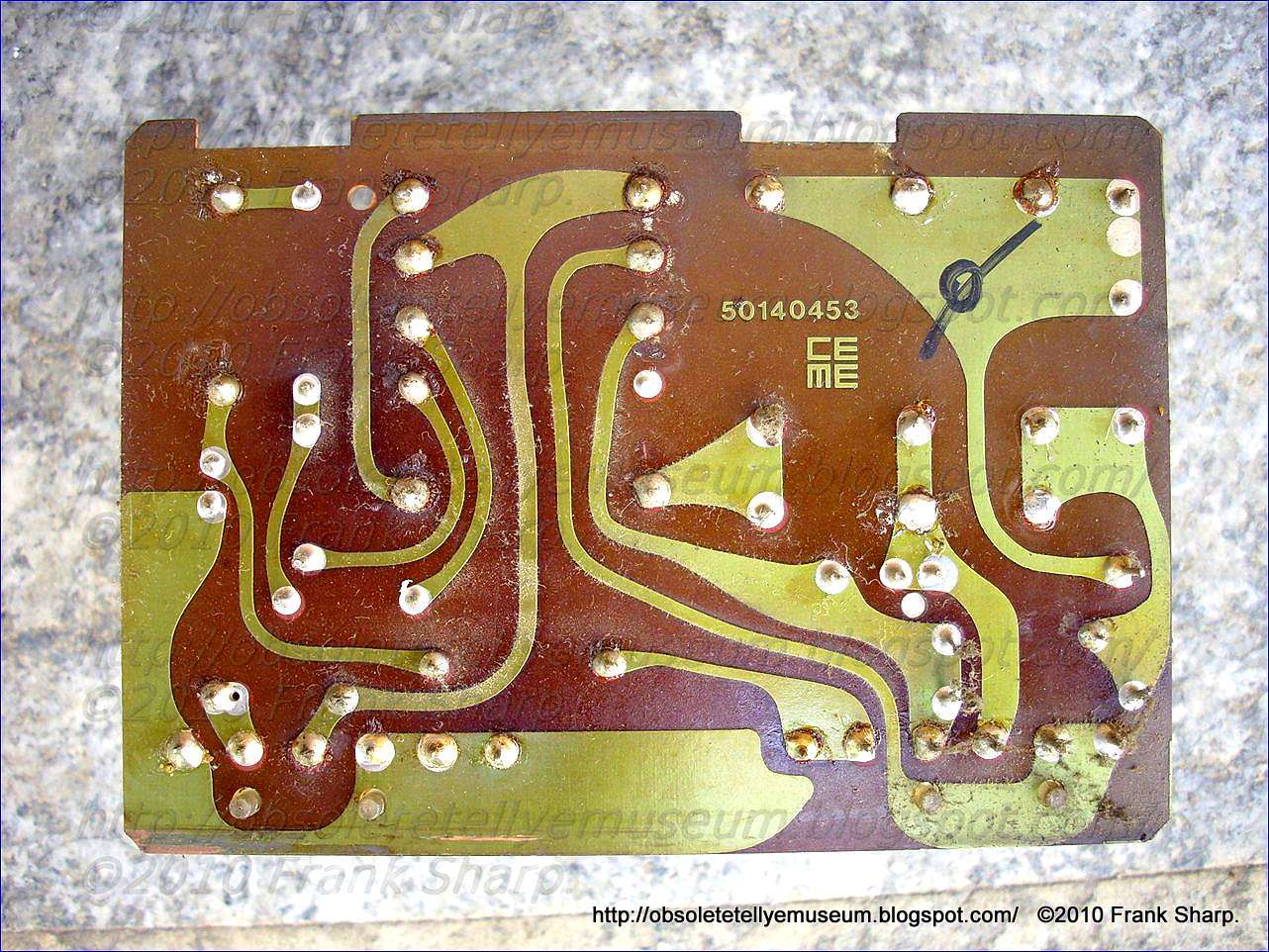


- Commutating / Switching Combi coil Unit 50140453
- E/W correction (Passive) Unit
- Line deflection Supply Regulator Unit 50140422
- RGB AMPL 50141260
- FRAME deflection oscillator 50140442
- Line oscillator + synch unit 50140471 TBA920
- Luminance + chrominance unit 50141320 TBA560C + TBA990 + TBA540
THE Philips TBA SERIES
The TBA series of i.c.s developed by Philips for use in TV receivers comprises the TBA500Q, TBA510Q, TBA520Q, TBA530Q, TBA540Q, TBA550Q, TBA560Q, TBA750Q and TBA990Q, the Q signifying that the lead out pins are in zig-zag form as illustrated in other posts here at Obsolete Technology Tellye !
The operations the various i.c.s in this series perform are as follows:
TBA500Q: Luminance Combination. Luminance amplifier for colour receivers incorporating luminance delay line matching stages, gated black level clamp and a d.c. contrast control which maintains a constant black level over its range of operation. A c.r.t. beam limiter facility is incorporated, first reducing the picture contrast and then the brightness. Line and field flyback blanking can also be applied.
TBA510Q: Chrominance Combination. Chrominance amplifier for colour receivers incorporating a gain controlled stage, a d.c. control for saturation which can be ganged to the receiver's contrast control, burst gating and blanking, a colour killer, and burst output and PAL delay line driver stages.
TBA520Q: Chrominance Demodulator. Incorporates U and V synchronous demodulators, G-Y matrix and PAL V switch. This type will be superseded by
the TBA990Q (development of which was nearing completion in 1972) listed later.
TBA530Q: RGB Matrix. Luminance and colour difference signal matrix incorporating preamplifiers.
TBA540Q: Reference Combination. Decoder reference oscillator (with external crystal) and a.p.c. loop. Also provides a.c.c., colour killer and ident outputs. TBA550Q: Video signal processor for colour or monochrome receivers. This i.c. is the successor to the TAA700. It is very similar electrically to the TAA700. TBA560Q: Luminance and Chrominance Combination. Provides luminance and chrominance signal channels for a colour receiver. Although not equivalent to the TBA500Q and TBA510Q it performs similar functions to those i.c.s.
TBA750Q: Intercarrier Sound Channel. Incorporates five stage intercarrier sound limiter/amplifier plus quadrature detector and audio preamplifier. External
TBA990Q: Chrominance Demodulator. Incorporates U and V synchronous demodulators, G -Y matrix and PAL V switch. This is at the time in the final stages of development and was been available from March 1972 onwards. As I have given information previously on the TBA550Q and TBA750Q we may concentrate in this and the concluding post in the series on the colour receiver i.c.s. such as multistandard sets or bistandard color decoders here at Obsolete Technology Tellye !
Fig. 1 shows in block diagram form their application for luminance and chrominance signal processing. We will look first at the TBA520Q an
 d TBA530Q which are in use for example in the Philips G8 single standard colour chassis.
TBA530Q RGB Matrix Preamplifier:
The internal circuitry of this i.c. is shown in Fig. 2 while Fig. 3 shows the immediate external connections as used in the Philips G8 chassis. The chip layout is designed to ensure tight thermal coupling between all transistors to minimise thermal drift between channels and each channel has an identical layout to the others to ensure equal frequency response characteristics. The colour -difference signals are fed in at pins 2, 3 and 4 and the luminance input is at pin 5. Trl and Tr2 form the matrix in each channel, driving the differential amplifiers Tr3, Tr4, Tr5. The operating conditions are set by Tr5 and Tr7, using an external current -determining resistor connected to pin 7. Pin 6 is the chassis connection and pin 8 the 12V supply line connection (maximum voltage permitted 13.2V, approximate current consumption 30mA). External load resistors are connected to pins 1, 14 and 11 from a 200V line and the outputs are taken from pins 16, 13 and 10. The output pins are internally connected to the load resistor pins via Tr6
 which provides a zener-type junction giving a level shift appropriate
for driving the bases of the external output transistors directly.
External l0kpF capacitors are required between the output and load
resistor pins to bypass these zener junctions at h.f. Feedback from the
external output stages is fed in at pins 15, 12 and 9. A common supply
line should be used for this and any other i.c.s in the series used in
the decoder, to ensure that any changes in the black level caused by
variations in the supply voltage occur in a predictable way : the
stability of the supply should be not worse than ±3% due to operational
variations to limit changes in picture black level during receiver
operation. To reduce the possibility of patterning on the picture due to
radiation of the harmonics of the demodulation
which provides a zener-type junction giving a level shift appropriate
for driving the bases of the external output transistors directly.
External l0kpF capacitors are required between the output and load
resistor pins to bypass these zener junctions at h.f. Feedback from the
external output stages is fed in at pins 15, 12 and 9. A common supply
line should be used for this and any other i.c.s in the series used in
the decoder, to ensure that any changes in the black level caused by
variations in the supply voltage occur in a predictable way : the
stability of the supply should be not worse than ±3% due to operational
variations to limit changes in picture black level during receiver
operation. To reduce the possibility of patterning on the picture due to
radiation of the harmonics of the demodulation process the leads carrying the drive signals to the tube should be kept
as short as possible : resistors (typically 1.51J) connected in series
with the leads and mounted close to the collectors of the out- put
transistors provide useful additional filtering of these harmonics.
process the leads carrying the drive signals to the tube should be kept
as short as possible : resistors (typically 1.51J) connected in series
with the leads and mounted close to the collectors of the out- put
transistors provide useful additional filtering of these harmonics. TBA520Q Chrominance Demodulator:
 In addition to U and V balanced synchronous detectors this i.c. incorporates a PAL switch which inverts on alternate lines the V reference signal fed to the V synchronous detector. The PAL switch is controlled by an integrated flip-flop circuit which is driven by line frequency pulses and is under the control of an ident input to synchronise the V switching. Outputs from the U and V demodulators are matrixed within the i.c. to obtain the G-Y signal so that all three colour difference signals are available at pins 4, 5 and 7. The internal circuit of this i.c. is shown in Fig. 4 while Fig. 5 shows the immediate external circuitry as used in the Philips G8 chassis. The separated U and ±V chrominance signals from the PAL delay line/matrix circuit are fed in at pins 9 and 13 respectively. The U and V reference signals, in phase quadrature, are fed in at pins 8 and 2. Taking the U channel first we see that the U chrominance signal is fed to Tr18 base. This transistor with Tr19 forms a differential pair which drives the emitters of the transistors-Tr4, Try, Tr6 and Tr7-which comprise the U synchronous demodulator. The U reference signal is fed to Tr12 base, this transistor with Tr13 forming a further differential pair which drive the bases of the synchronous demodulator transistors. The B -Y signal is developed across R3 and appears at output pin 7. A similar arrangement is followed in the V channel except that here the V reference signal fed in at pin 2 to the base of Tr22 is routed to the V synchronous demodulator (Tr8-Tr11) via the PAL switch Tr14-Tr17. This switch is controlled by the integrated flip-flop (bistable) Tr24 and Tr25 (with diodes DI and D2). The bases of the transistors in the flip-flop circuit are driven by negative goin
 g
line frequency pulses fed in at pins 14 and 15. As a result half line
frequency antiphase squarewaves are developed across R13 and R14 and fed
to the PAL switch via R57 and R58. The ident signal is fed into the
base of Tr32 at pin 1. A positive -going input to pin 1 drives Tr32 on
so that the base of Tr24 is shorted and the flip-flop rendered inactive
until the positive input is removed. In the Philips circuit a 4V peak
-to -peak 7.8kHz sinewave ident signal is fed in at pin 1 to synchronise
the flip-flop. The squarewave signal is externally available at pin 3
from the emitter -follower Tr39 which requires an external load
resistor. The R-Y signal developed across R9 is fed via R10 to output
pin 4. The G-Y signal appears at the output of the matrix network R4, R5
and R6 and is fed via R7 to pin 5. The d.c. voltages applied to pins 11
and 12 establish the correct G -Y and R-Y signal levels relative to the
B -Y signal. Pin 10 is internally connected and no external connection
should be made to this pin. The U and V reference carrier inputs should
be about IV p -p, via a d.c. blocking capacitor in each feed. These
inputs must not be less than 0-5V. The flip-flop starts when the voltage
at pin 1 is reduced The amplitudes of the pulses fed in at pins 14 and
15 below 0.4V : it should not be allowed to exceed -5V. to drive the
flip-flop should be between 2.5 and 5V p-p.
g
line frequency pulses fed in at pins 14 and 15. As a result half line
frequency antiphase squarewaves are developed across R13 and R14 and fed
to the PAL switch via R57 and R58. The ident signal is fed into the
base of Tr32 at pin 1. A positive -going input to pin 1 drives Tr32 on
so that the base of Tr24 is shorted and the flip-flop rendered inactive
until the positive input is removed. In the Philips circuit a 4V peak
-to -peak 7.8kHz sinewave ident signal is fed in at pin 1 to synchronise
the flip-flop. The squarewave signal is externally available at pin 3
from the emitter -follower Tr39 which requires an external load
resistor. The R-Y signal developed across R9 is fed via R10 to output
pin 4. The G-Y signal appears at the output of the matrix network R4, R5
and R6 and is fed via R7 to pin 5. The d.c. voltages applied to pins 11
and 12 establish the correct G -Y and R-Y signal levels relative to the
B -Y signal. Pin 10 is internally connected and no external connection
should be made to this pin. The U and V reference carrier inputs should
be about IV p -p, via a d.c. blocking capacitor in each feed. These
inputs must not be less than 0-5V. The flip-flop starts when the voltage
at pin 1 is reduced The amplitudes of the pulses fed in at pins 14 and
15 below 0.4V : it should not be allowed to exceed -5V. to drive the
flip-flop should be between 2.5 and 5V p-p. For a colou bar signal a U input of approximately 360mV is required at pin 9 and a V input of approximately 500mV is required at pin 13. The supply is fed in at pin 6 and this also sets the d.c. level of the B-Y output signal. The maximum voltage allowed at this pin is 13.2V. In early versions of the Philips G8 chassis a TAA630 i.c. was used in place of the TBA520Q.
Philips TBA SERIES SINCE the last part in this series Philips have released details of a PAL -D decoder developed in their laboratories in which most of the circuitry has been integrated into four i.c.s a TBA560Q which undertakes the luminance and chrominance signal processing, a TBA540Q which provides the reference signal channel, a TBA990Q which provides synchronous demodulation of the colour -difference signals, G -Y signal matrixing and PAL V switching, and a TBA530Q which matrixes the colour -difference signals and the luminance signal to obtain the R, G and B signals which after amplification by single -transistor output stages drive the cathodes of the shadowmask tube.
The TBA540Q and TBA560Q and also the TBA500Q and TBA510Q which provide an alternative luminance and chrominance signal processing arrangement will be covered this time.
The internal circuits of the TBA530Q and TBA520Q (predecessor to the TBA990Q which shows how fast things are moving at present) were shown in Part 6 in order to give an idea of the type of circuitry used in these linear colour receiver i.c.s. The internal circuitry is not however of great importance to the user or service engineer: all we need to know about a particular i.c. are the functions it performs, the inputs and outputs it requires and provides and the external connections necessary. The i.c.s we shall deal with in this instalment are highly complex internally the TBA560Q for example contains some 67 integrated transistor elements alone. This time therefore we shall just show the immediate external circuitry in conjunction with a block diagram to indicate the functions performed within the i.c.
TBA540Q Reference Signal Channel:

A block diagram with external connections for this i.c. is shown in Fig. 1. In addition to providing the reference signal required for synchronous demodulation of the colour difference signals this i.c. incorporates automatic phase and amplitude control of the reference oscillator and a half line frequency synchronous demodulator which compares the phases and amplitudes of the burst ripple and the square waveform from the PAL V switch circuit in order to generate a.c.c., colour killer and ident outputs. The use of a synchronous demodulator for these functions provides a high standard of noise immunity in the decoder. The internal reference oscillator operates in conjunction with an external 4.43MHz crystal connected between pins 1 and 15. The nominal load capacitance of the crystal is 20pF. The reference oscillator output, in correct phase for feeding to the V signal synchronous demodulator, is taken from pin 4 at a nominal amplitude of 1.5V peak -to -peak. This is a low -impedance output and no d.c. load to earth is required here. The bifilar inductor Ll provides the antiphase signal necessary for push-pull reference signal drive to the burst detector circuit, the antiphase input being at pin 6. The U subcarrier is obtained from the junction of a 900 phase shift network (R1, C1) connected across Ll. The oscillator is controlled by the output at pin 2. This pin is fed internally with a sinewave derived from the reference signal and controlled in amplitude by the internal reactance control circuit. The phase of the feedback from pin 2 to the crystal via C2 is such that the value of C2 is effectively increased. Pin 2 is held internally at a very low impedance. Thus the tuning of the crystal is automatically controlled by the amplitude of the feedback waveform and its influence on the effective value of C2. The burst signal is fed in at pin 5. A burst waveform amplitude of 1V peak -to -peak is required (the minimum threshold is 0.7V) and this is a.c. coupled. The a.p.c. loop phase detector (burst detector) loads and filter (R2, C4, C5 and C6) are connected to pins 13 and 14. A synchronously -generated a.c.c. potential is produced at pin 9. The voltage at this pin is set by R3 to 4V with zero burst input. The synchronous demodu- lator producing this output is fed with the burst signal and the PAL half line frequency squarewave which is a.c. coupled at pin 8 at 2.5V peak -to -peak. If the phase of the squarewave is correct the potential at pin 9 will fall and normal a.c.c. action will commence. If the phase of the squarewave is incorrect the voltage at pin 9 will rise, providing the ident action as this rise will make the PAL switch miss a count thereby correcting its phase. A colour -killer output is provided at pin 7 from an internal switching transistor. If the ident conditions are incorrect this transistor is saturated and the output at pin 7 is about 250mV. When the ident conditions are correct (voltage at pin 9 below 2.5V) the transistor is cut off providing a positive -going turn -on bias at pin 7. The network between pins 10 and 12 provides filtering and a.c.c. level (R3) setting. The control connected to pin 11 is set so that in conjunction with the rest of the decoder circuitry the level of the burst signal at pin 5 under a.c.c. control is correct. The positive d.c. supply required is applied to pin 3 and the chassis connection is pin 16.
TBA560Q Chroma-Luminance IC:

A block diagram with external connections for this i.c. is shown in Fig. 2. The i.c. incorporates the circuits required to process the luminance and chrominance signals, providing a luminance output for the RGB matrix and a chrominance output for the PAL delay line circuit.
The luminance input is a.c. coupled from the luminance delay line terminating resistor at pin 3. This pin also requires a d.c. bias current which is obtained via the 22kI resistor shown. The brightness control is connected to pin 6: variation from OV to 1 2V at this pin gives a variation in the black level of the luminance output at pin 5 of from OV to 3V, which is a greater range than is needed in practice. The contrast control is connected to pin 2 and the potential applied here controls the gain of both the luminance and the chrominance channels so that the two signals track together correctly. Picture tube beam current limiting can be applied at either pin 6 or pin 2 (by taking the earthy side of one of the controls to a beam limiter network). To maintain correct picture black level it is preferable to apply the beam limiting facility to reduce the contrast. A positive going pulse timed to coincide with the back porch period is fed in at pin 10 to provide burst gating and to operate the black -level clamp in the luminance channel: the black -level clamp requires a charge storage capacitor which is connected to pin 4. The luminance output is obtained from an internal emitter follower at pin 5, an external load resistor of not less than 2kS2 being required here. The output has a nominal black level of 1.6V and 1V black -to -white amplitude. The chrominance signal is applied in push-pull to pins 1 and 15. A.c.c. is applied at pin 14, a negative going potential giving a 26dB control range starting at 1V and giving maximum gain reduction at 200mV. The saturation control is connected to pin 13 and the colour -killer potential is also applied to this pin : the chrominance channel is muted when the voltage at this pin falls below IV. The chrominance output, at an amplitude of about 2V peak -to -peak, is obtained at pin 9: an external network is required which provides d.c. negative feedback in the chrominance channel via pin 12. The burst output, at about 1V peak -to -peak, is obtained at pin 7. A network connected to this pin also provides d.c. feedback to the chrominance input transformer (connected between pins 1 and 15) to give good d.c. stability. Line and field blanking pulses are fed in at pin 8 to the luminance and chrominance channels : these negative -going pulses should not exceed -5V in amplitude. The d.c. supply is applied to pin 11 and pin 16 is the chassis connection.
TBA500Q Luminance IC:
A block diagram with external connections for this i.c. is shown in Fig. 3. This i.c. provides a colour receiver luminance channel incorporating luminance delay -line matching stages, a black -level clamp and a d.c. contrast control which maintains a constant black level over its range of operation. A beam current limiting facility which first reduces picture ,contrast and then picture brightness is provided and line and field flyback blanking can be applied. A video input signal of 2V peak -to -peak with negative -going sync pulses is required at pin 2, a.c. coupled. A clamp potential obtained from pin 13 via a smoothing circuit is fed to pin 2 to regulate the black level of the signal at pin 2 to about 10-4V. The smoothing network for the black -level control potential should have a time -constant which is less than the time constant of the video signal coupling network. The 3V peak -to -peak composite video output with positive -going sync pulses obtained at pin 3 from an emitter -follower can be used as a source of chroma signal: in Fig. 3 it is used as a source of sync pulses for the black -level clamp, fed in at pin 15. This pin requires positive -going sync pulses of 2V amplitude or greater for sync -cancelling the black -level clamp. The other input to the clamp consists of negative going back porch pulses fed in at pin 1 to operate th
 e
clamp. The timing of these pulses is not critical provided the pulse
does not encroach on the sync pulse period and that it dwells for at
least Zus on any part of the back porch-clamp pulse overlap into the
picture line period is unimportant. A low-pass filter capacitor for the
clamp is connected at pin 14 to prevent the operation of the clamp being
affected by the bursts or h.f. noise. The contrast control is connected
to pin 5 and is linked to the saturation control so that the two track
together. A variation of from 2 to 4V at pin 5 gives a control range of
at least 40dB, the relationship between the video at pin 4 and the
potential at pin 5 being linear. An output to drive the luminance delay
line is provided at pin 4. This is a low -impedance source and a
luminance delay line with a characteristic impedance of 1-2.7161 can be
used. The delayed luminance signal is fed back into the i.c. at pin 8.
Line and field flyback banking pulses and the brightness control are
also connected to this pin. The gain of the luminance channel is
determined by the value of the resistor connected to pin 9. The
luminance output is taken from an emitter -follower at pin 10, an
external load resistor being required. The voltage output range
available is from 0.7V to 5-5V. The potential of the black level of the
output signal is normally set to 1.5V by appropriate setting of the
potential at pin 8. A luminance signal output amplitude of 2.8V black to
white at maximum contrast is produced : superimposed on this is the
blanking waveform which remains of constant amplitude independently of
the contrast and brightness control settings. A beam current limiting
input is provided at pin 6. A rising positive potential at this pin will
start to reduce the contrast at about 2V. Further increase in the
voltage at this pin will continue to reduce the contrast until a
threshold is reached, determined by the potential applied to pin 7, when
the d.c. level of the video signal is reduced giving reduction in
picture brightness. The d.c. supply is connected to pin 12 and pin 16 is
the chassis connection.
e
clamp. The timing of these pulses is not critical provided the pulse
does not encroach on the sync pulse period and that it dwells for at
least Zus on any part of the back porch-clamp pulse overlap into the
picture line period is unimportant. A low-pass filter capacitor for the
clamp is connected at pin 14 to prevent the operation of the clamp being
affected by the bursts or h.f. noise. The contrast control is connected
to pin 5 and is linked to the saturation control so that the two track
together. A variation of from 2 to 4V at pin 5 gives a control range of
at least 40dB, the relationship between the video at pin 4 and the
potential at pin 5 being linear. An output to drive the luminance delay
line is provided at pin 4. This is a low -impedance source and a
luminance delay line with a characteristic impedance of 1-2.7161 can be
used. The delayed luminance signal is fed back into the i.c. at pin 8.
Line and field flyback banking pulses and the brightness control are
also connected to this pin. The gain of the luminance channel is
determined by the value of the resistor connected to pin 9. The
luminance output is taken from an emitter -follower at pin 10, an
external load resistor being required. The voltage output range
available is from 0.7V to 5-5V. The potential of the black level of the
output signal is normally set to 1.5V by appropriate setting of the
potential at pin 8. A luminance signal output amplitude of 2.8V black to
white at maximum contrast is produced : superimposed on this is the
blanking waveform which remains of constant amplitude independently of
the contrast and brightness control settings. A beam current limiting
input is provided at pin 6. A rising positive potential at this pin will
start to reduce the contrast at about 2V. Further increase in the
voltage at this pin will continue to reduce the contrast until a
threshold is reached, determined by the potential applied to pin 7, when
the d.c. level of the video signal is reduced giving reduction in
picture brightness. The d.c. supply is connected to pin 12 and pin 16 is
the chassis connection.TBA510Q Chrominance IC:

A block diagram with external connections for this i.c. is shown in Fig. 4. It provides a colour receiver chrominance signal processing channel with a variable gain a.c.c. chroma amplifier circuit, d.c. control of chroma saturation which can be ganged to the opera- tion of the contrast control, chroma blanking and burst gating, a burst output stage, colour -killer circuit and PAL delay line driver stage. The chroma signal is a.c. coupled to pin 4, the a.c.c. control potential being applied at pin 2. The non - signal side of the differential amplifier used for the a.c.c. system is taken to pin 3 where a decoupling capacitor should be connected. A resistor can be connected between pins 2 and 3 to reduce the control sensitivity of the a.c.c. system to any desired level. The saturation control is connected to pin 15, the d.c. control voltage range required here being 1.5-4-5V. For chrominance blanking a negative -going line flyback pulse of amplitude not greater than 5V is fed in at pin 14. A series network is connected to pin 6 to decouple the emitter of one of the amplifying stages in the i.c.: the value of the resistor in this network influences the gain of both the burst and the chroma channels in the i.c. The chrominance signal outputs are obtained at pin 8 (collector) to drive the chroma delay line and pin 9 (emitter) to feed the chrominance signal matrix (undelayed signal). A resistive path to earth is essen- tial at pin 9. The colour -killer turn -on bias is applied to pin 5 : colour is "on" at 2.3V, "off" at 1.9V. Chroma signal suppression when killed is greater than 50dB. The burst signal output is at pin 11 (collector) or 12 (emitter). If a low -impedance output is required pin 11 is connected direct to the 12V supply rail and the output is taken from pin 12. An external load of 2kn connected to chassis is required here. The burst gating pulse is fed in at pin 13, a negative -going pulse of not greater than 5V amplitude being required. Pins 7 and 10 are connected to an internal screen whose purpose is to prevent unwanted burst and chroma outputs : the pins must be linked together and taken via a direct path to earth. Pin 1 is the d.c.
supply pin and pin 16 the chassis connection.
A TBA510 as example is used in the Grundig 1500/3010 series and also the YR 1972 Grundig colour chassis (5010 / 5050 series) introduced in the70's. Grundig continue in these models to favour colour -difference tube drive. The 5010 series uses a TBA510 together with a TAA630 colour demodulator i.c. in the chrominance section and a TBA970 luminance i.c. which drives a single BF458 luminance output transistor operated from a 280V rail. As this series has been appearing more and more i.c.s have come to be used in television receivers, both monochrome and colour, and more and more i.c.s designed for television set use have been announced. Some of these have been mentioned in recent argumentations here in this Web Museum. There seems little doubt that a major increase in the use of integrated circuits in television receivers is about to occur in the future. Fully integrated i.f. and vision detector sections are already in use (PHILIPS K9-K11) and this is the likely area, together with the decoder in colour sets, in which integration will most rapidly spread. Elsewhere integrated line and field oscillators using circuits without inductors have been developed and a field output stage in integrated form is now feasible. Line output stages consisting of hybrid i.c. and thick film circuits (PHILIPS K12) have been built and there is a programme of work directed to the integration of the r.f. tuner, using digital frequency synthesisers to provide local oscillator action controlled by signals from a remote point.
We seem to have reached the position where the only part of the set which does not attract the i.c. manufacturers is the picture tube itself !
TBA920 line oscillator combination
 DESCRIPTION
The line oscillator combination TBA920 is a monolithic
integrated circuit intended for the horizontal deflection of the black and white
and colour TV sets
picture tube.
FEATURES:
SYNC-PULSE SEPARATION
OPTIONAL NOISE INVERSION
GENERATION OF A LINE FREQUENCY VOL-
TAGE BY MEANS OF AN OSCILLATOR
PHASE COMPARISON BETWEEN SYNC-
PULSE AND THE OSCILLATOR WAVEFORM
PHASE COMPARISON BETWEEN THE OS-
CILLATOR WAVEFORM AND THE MIDDLE OF
THE LINE FLY-BACK PULSE
AUTOMATIC SWITCHING OF THE VARIABLE
TRANSCONDUCTANCE AND THE VARIABLE
TIME CONSTANT TO ACHIEVE NOISE SUP-
PRESSION AND, BY SWITCHING OFF, POS-
SIBILITY OF TAPE-VIDEO-REGISTERED RE-
PRODUCTION
SHAPING AND AMPLIFICATION OF THE OS-
CILLATOR WAVEFORM TO OBTAIN PULSES
FOR THE CONTROL OF DRIVING STAGES IN
HORIZONTAL, DEFLECTION CIRCUITS
USING EITHER TRANSISTORS OR THYRISTORS
No comments:
Post a Comment
The most important thing to remember about the Comment Rules is this:
The determination of whether any comment is in compliance is at the sole discretion of this blog’s owner.
Comments on this blog may be blocked or deleted at any time.
Fair people are getting fair reply. Spam and useless crap and filthy comments / scrapers / observations goes all directly to My Private HELL without even appearing in public !!!
The fact that a comment is permitted in no way constitutes an endorsement of any view expressed, fact alleged, or link provided in that comment by the administrator of this site.
This means that there may be a delay between the submission and the eventual appearance of your comment.
Requiring blog comments to obey well-defined rules does not infringe on the free speech of commenters.
Resisting the tide of post-modernity may be difficult, but I will attempt it anyway.
Your choice.........Live or DIE.
That indeed is where your liberty lies.
Note: Only a member of this blog may post a comment.