


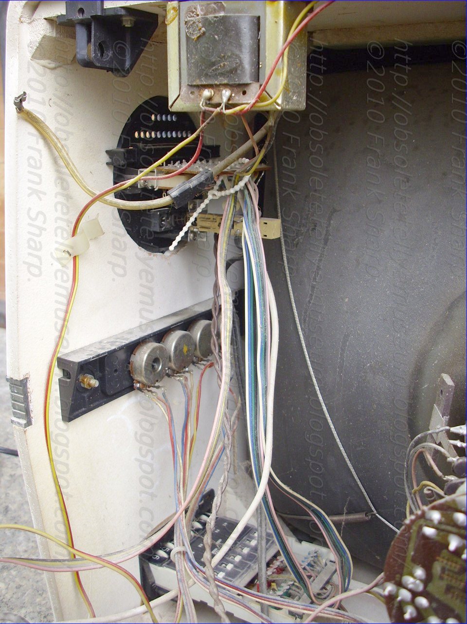

This PHONOLA is fitted with a PHILIPS Chassis CHASSIS TI-22 with a few tubes
- PL504
- PY88
- PCL805
and many transistor mainly germanium technology and even an ASIC IC TBA750.
BF195, BF196, BF197. B157, BC177, MJE340
- The EHT Output is realized with a selenium rectifier.
The EHT s
elenium rectifier which is a Specially designed selenium rectifiers were once widely used as EHT rectifiers in television sets and photocopiers. A layer of selenium was applied to a sheet of soft iron foil, and thousands of tiny discs (typically 2mm diameter) were punched out of this and assembled as "stacks" inside ceramic tubes. Rectifiers capable of supplying tens of thousands of volts could be made this way. Their internal resistance was extremely high, but most EHT applications only required a few hundred microamps at most, so this was not normally an issue. The rectifier is fed from a high voltage pulse transformer T1 connected
to an EHT source such as the synchronization flyback circuit of a
television receiver.; Each rectifier stack comprises an assembly of
selenium discs in an insulating tube provided with end terminals. The
stacks and the capacitor C may be mounted in clips on a plastic panel
screwed to the casing of the transformer T1. With the development of inexpensive high voltage silicon rectifiers, this technology has fallen into disuse. How AFC Circuit Works in B/W Analog Television Receiver:
 Push-Button
tuning on u.h.f. while being very convenient often leaves a margin of
mistuning, especially after some wear and tear has occurred on the
mechanism. Even dial tuning can lead to errors due to the difficulty
many people experience in judging the correct point. Oscillator drift
due to temperature changes can also cause mistuning. Automatic frequency
control (a.f.c.) will correct all these faults. The vision carrier when
the set is correctly tuned on u.h.f. is at 39.5MHz as it passes down
the i.f. strip. Thus if at the end of the i.f. strip a discriminator
tuned circuit is incorporated centred on 39.5MHz the discriminator
output will be zero at 39.5MHz and will move positively' one side of
39.5MHz and negatively the other as the tuning drifts. This response is
shown in Fig. 1.
Push-Button
tuning on u.h.f. while being very convenient often leaves a margin of
mistuning, especially after some wear and tear has occurred on the
mechanism. Even dial tuning can lead to errors due to the difficulty
many people experience in judging the correct point. Oscillator drift
due to temperature changes can also cause mistuning. Automatic frequency
control (a.f.c.) will correct all these faults. The vision carrier when
the set is correctly tuned on u.h.f. is at 39.5MHz as it passes down
the i.f. strip. Thus if at the end of the i.f. strip a discriminator
tuned circuit is incorporated centred on 39.5MHz the discriminator
output will be zero at 39.5MHz and will move positively' one side of
39.5MHz and negatively the other as the tuning drifts. This response is
shown in Fig. 1.If the tuning is not correct then the discriminator output is not zero and if this output is applied to change the reverse bias on a tuning diode mounted in the oscillator section of the u.h.f. tuner it will correct most of the error. Tuning, varicap or varactor diodes-to give them a few of their names-are junction diodes normally operated with reverse bias but not sufficient to bias them into the breakdown region in which zener diodes operate. The greater the reverse bias the lower their capacitance: a typical curve, for the PHILIPS BB105 or STC BA141 tuning diode, is shown in Fig. 2. All diodes e
 xhibit
this basic type of characteristic but special diodes have to be used
for u.h.f. because they must not introduce any excessive loss into the
tuned circuits they control. In other words, just as a coil has to have a
good Q so does a varicap diode. Normally, we don't worry about the Q of
a capacitor as it is usually very good. However, a tuning diode is not a
true capacitor. It has, for example, leakage current so the Q of the
diode is a factor which has to be considered. The diode manufacturer
however will have considered these points and if you buy a diode
specified for u.h.f. use you will have no trouble. These points have
been mentioned to clear up any misunderstandings and to show why any old
diode won't do.
xhibit
this basic type of characteristic but special diodes have to be used
for u.h.f. because they must not introduce any excessive loss into the
tuned circuits they control. In other words, just as a coil has to have a
good Q so does a varicap diode. Normally, we don't worry about the Q of
a capacitor as it is usually very good. However, a tuning diode is not a
true capacitor. It has, for example, leakage current so the Q of the
diode is a factor which has to be considered. The diode manufacturer
however will have considered these points and if you buy a diode
specified for u.h.f. use you will have no trouble. These points have
been mentioned to clear up any misunderstandings and to show why any old
diode won't do.Basic AFC System
To return to our TV set, if the oscillator frequency is too high then the vision carrier frequency will also be too high and in the simple arrangement shown in Fig. 3 the discriminator will give a negative signal to decrease the bias on the tuning diode thus increasing its
 capacitance
and in turn reducing the oscillator frequency and correcting the error.
Note that in this diagram the reverse bias on the diode is applied to
its cathode. It is therefore positive with respect to ground so that a
negative signal from the discriminator will reduce the positive voltage
on the diode thus reducing its bias and increasing its capacitance. In
this arrangement the diode is biased somewhere near the mid point of its
characteristic by the positive d.c. bias fed into one side of the
discriminator. The discriminator thus adds to or subtracts from this
d.c. bias.
capacitance
and in turn reducing the oscillator frequency and correcting the error.
Note that in this diagram the reverse bias on the diode is applied to
its cathode. It is therefore positive with respect to ground so that a
negative signal from the discriminator will reduce the positive voltage
on the diode thus reducing its bias and increasing its capacitance. In
this arrangement the diode is biased somewhere near the mid point of its
characteristic by the positive d.c. bias fed into one side of the
discriminator. The discriminator thus adds to or subtracts from this
d.c. bias.AFC Loop Gain:
The amount by which the error is reduced depends on the gain of the circuit. An estimate of the gain required must first be made by guessing how much error is likely to be given by your push -buttons or hand tuning: 1MHz would be an outside figure as a tuning error of that magnitude would produce a very bad picture of low definition in one direction and badly broken up in the other. This error should be reduced to
 about
100kHz to be really unnoticeable, indicating a required gain of ten. In
fitting a.f.c. to an existing set some measure- ments should be done as
an experiment before finally deciding on the circuit gain. The first
thing to do is to add the suggested discriminator to the i.f. strip. As
the circuit (Fig. 4) shows a Foster -Seeley type discriminator is used
and with the coils specified and the driver circuit shown it should give
±4V for 0.5MHz input variation.
about
100kHz to be really unnoticeable, indicating a required gain of ten. In
fitting a.f.c. to an existing set some measure- ments should be done as
an experiment before finally deciding on the circuit gain. The first
thing to do is to add the suggested discriminator to the i.f. strip. As
the circuit (Fig. 4) shows a Foster -Seeley type discriminator is used
and with the coils specified and the driver circuit shown it should give
±4V for 0.5MHz input variation.EXAMPLE of Circuit Description:
The driver stage Tr1 takes a small sample signal from the i.f. strip but this should be large enough to drive Tr1 into saturation. That is to say Tr1 is a limiter stage so that the signal amplitude applied to the discriminator coil L2 stays constant over the normal range of signal levels. Trl is biased at approximately 7mA which, according to the original report ("Simple a.f.c. system for 625 -line TV receivers" by P. Bissmire, PHILIPS Technical Communications, March, 1970), gives the best limiting performance. C1, R
 14
and R3 damp the stage to prevent oscillation. C2 decouples the power
feed and should be close to the circuit. The coil former and can are the
normal ones used for TV sets and so should be easily obtainable: the
former diameter is 5mm. and length 40mm. and winding details are given
in Fig. 5.
14
and R3 damp the stage to prevent oscillation. C2 decouples the power
feed and should be close to the circuit. The coil former and can are the
normal ones used for TV sets and so should be easily obtainable: the
former diameter is 5mm. and length 40mm. and winding details are given
in Fig. 5.The invention being thus described, it will be obvious that the same may be varied in many ways. Such variations are not to be regarded as a departure from the spirit and scope of the invention, and all such modifications as would be obvious to one skilled in the art are intended to be included within the scope of the developed apparates both tubes or transistors.
PHONOLA MOD. 2028 CHASSIS TI-22 CIRCUIT ARRANGEMENT FOR PRODUCING A SAWTOOTH CURRENT ACROSS THE VERTICAL DEFLECTION COIL OF A TELEVISION RECEIVER, Philips Tubes vertical deflection
A circuit for introducing adjustable parabolic and S-components in a sawtooth curr
 ent
in a coil, wherein the coil is connected in the output of an amplifier
device, con-sists of the series circuit of a charging capacitor, a
wind-ing coupled to the coil, and a first resistor. A first series
circuit of a second resistor and a reservoir capacitor is connected
between the junction of the first resistor and winding and the junction
of the winding and charging ca-pacitor, in that order. The junction of
the second re-sistor and second capacitor are connected to the control
electrode of the amplifier. The other end of the charging capacitor is
connected to a variable tapping on a parallel resistance capacitance
circuit in another input circuit of the device, in order to permit
varying of the relative am-plitudes of the parabolic and S-components. A
variable resistor is connected between the control electrode and the
variable tapping in order to permit variation of the am-plitudes of the
parabolic and S-component with respect to the sawtooth component.
ent
in a coil, wherein the coil is connected in the output of an amplifier
device, con-sists of the series circuit of a charging capacitor, a
wind-ing coupled to the coil, and a first resistor. A first series
circuit of a second resistor and a reservoir capacitor is connected
between the junction of the first resistor and winding and the junction
of the winding and charging ca-pacitor, in that order. The junction of
the second re-sistor and second capacitor are connected to the control
electrode of the amplifier. The other end of the charging capacitor is
connected to a variable tapping on a parallel resistance capacitance
circuit in another input circuit of the device, in order to permit
varying of the relative am-plitudes of the parabolic and S-components. A
variable resistor is connected between the control electrode and the
variable tapping in order to permit variation of the am-plitudes of the
parabolic and S-component with respect to the sawtooth component. The invention relates to a circuit arrangement for producing a sawtooth current across the vertical deflection coil of a television receiver. The coil is included in the output circuit of the vertical output stage, to the control-electrode of which is applied the sawtooth con-trol-signal which is developed across a charging capacitor included in the control-electrode circuit. The charging capacitor is periodicall
y discharged and is recharged with the aid of a charging
circuit which includes the se-ries combination of a resistor and a
winding, lying outside the discharging circuit. The winding is
magnetically cou-pled with a choke included in the output circuit of
the 50 vertical output stage, through which winding a voltage is
induced, which is opposite the capacitor voltage. Said winding has
connected with it in parallel the series corn-bination of at least one
resistor and one reservoir capaci-tor, the free end of the latter being
connected to the June- 55 tion of the charging capacitor and the
winding. A furher input electrode of the output stage has connected to
it the parallel combination of a resistor and a capacitor. One end of a
further resistor is connected to the control electrode of the vertical
output stage, and the other end GO of the further resistor is coupled
with the resistor con-nected to the said input electrode. Such a
circuit arrangement is described in U.S. Patent No. 2,851,632. It is,
however, necessary to add to each cycle of the sal,vtooth current one
cycle of a parabola 65 component and also one cycle of a so-called
&com-ponent. The parabola component is required in view of the
fact that the vertical deflection coil is coupled through a
trans-former with the vertical output stage. The same applies 70 to the
case in which for other reasons than coupling through the transformer
not only the vertical deflection3,426,243 Patented Feb. 4, 1969
coil, behaving substantially like a resistor, but also an in-ductor is included in the output circuit of the vertical final stage.
The S-component is required in view of the fact that the display screen of the display tube in a television re-ceiver is flat. Therefore, the rate of deflection of the electron beam must be higher at the centre of the screen than at the edge in order to achieve a linear displacement of the spot on the display screen. The S indicates sym-bolically what form the current through the deflection coil must be for obtaining these desired deflection rates. Numerous circuit arrangements are known by which the desired current form can be produced. However, they have the disadvantage that they are either too compli-cated or are not capable of providing the correct ratio between the sawtooth, parabola and S-component. The circuit arrangement according to the invention is, on the contrary, simple and provides, in addition, the possibility of adjusting accurately the desired ratio between saw-tooth, parabola and S-component, while it prevents, in addition, an excessive influence of undesirable higher de-gree components in the produced current. In order to produce the parabola and S-component, and permit adjustment of their amplitudes, the circuit arrangement according to the invention is characterized in that in parallel with the reservoir capacitor there is con-nected an integrating network which consists of the series combination of an integrating capacitor and an integrating resistor, the free end of the latter being coupled with the junction of the charging capacitor and of the reservoir capacitor.
The junction of the integrating resistor and the integrating capacitor is connected to the control-electrode of the output stage. The end of the charging capacitor remote from the winding is connected to a variable tap-ping of the resistor connected to the input electrode. The impedance of the latter resistor is, in operation, great with respect to the impedance of the comparatively great parallel-connected capacitor. In addition, the further re-sistor is made variable, and the end thereof not connected to the control electrode is connected to the tapping of the resistor connected to the input electrode. Variation of the tapping point adjusts the relative ampltiudes of the parab-ola and S-component, while variation of the further resistor controls the relative amplitudes of the parabola and S-component with respect to the sawtooth. A few possible embodiments of circuit arrangements according to the invention will be described with reference to the accompanying figures, of which FIG. 1 shows a possible circuit diagram of an embodi-ment equipped with valves. FIG. 2 shows a partial substitute diagram of the ar-rangement of FIG. I. FIG. 3 shows a further diagrammatical substitute dia-gram of the arrangement of FIG. 2. FIG. 4 shows a first possible modification of the sub-stitute diagram of FIG. 3 and hence of the arrangement of FIG. I and FIG. 5 shows a second possible modification of the substitute diagram of FIG. 3 and hence also of the ar-rangement of FIG. 1. Referring to FIG. 1, the valve 1 is the vertical output stage of a television receiver, the anode circuit of which includes an output transformer 2. The vertical deflec-tion coil 4 is connected to the secondary winding 3 of said transformer 2. In order to produce the desired control-voltage for the control-electrode 5 o
 f
the valve 1, the grid circuit of said valve includes the following
network. This net-work consists in the first place of a charging
resistor 6, a winding 7 and a charging capacitor 8, which are connected
in series with each other and the free end of the charging resistor 6
is connected to the positive supply voltage +VB. In practice the
voltage +VB is usually derived from the horizontal output stage, since
this stage is, in the first place stabilised and is, in addi-tion
capable of providing a fairly high supply voltage, which is conducive
to the linearity of the sawtooth volt-age to be produced. It will be
seen from FIG. 1 that the end of the capacitor 8 remote from the
winding 7 is connected, in accordance with a first principle of the
invention, to a variable tapping 9 associated with a po-tentiometer 10,
which is included in the cathode con-ductor of the valve 1. This
resistor is shunted by a com-paratively large electrolytic capacitor
11, which is chosen so that its impedance is small for the repetition
frequency of the sawtooth voltage to be produced with respect to the
impedance of the resistor 10. As is in-dicated by the line 12 with the
double arrow, the wind-ing 7 is magnetically coupled with the primary
winding of the transformer 2. As is the case in said Patent No.
2,851,632 the sense of winding of the winding 7 is such that the
sawtooth voltage 13 produced across the wind- 90 ing 7 is unlike the
sawtooth voltage 14 produced across the capacitor 8. Also in this case
this serves to ensure an optimum linearity of the sawtooth 14. The
winding 7 has furthermore connected with it in parallel the series
combination of a capacitor 15 and two resistors 16 and 17, the resistor
17 being variable. The network 15, 16 and 17 is provided for
eliminating the peak developed across the winding 7 during the vertical
fly-back from the signal 13, so that a signal 18 is finally produced
across the capacitor 15, the polarity of this signal being opposite
that of the voltage 14 across the capacitor 8, its waveform being,
however, substantially identical to that of the latter. For this
purpose the capacitor 15 must have a comparatively high value: a value
of 68K pf. may be chosen and the resistors 16 and 17 serving as peak
resistors must be comparatively small; values of 22K ohms and 10K ohms
respectively may be chosen. According to a further aspect of the
arrangement ac-cording to the invention the sawtooth voltage 18 is
em-ployed for producing partly the required parabola com-ponent and
partly the desired S-component. As will be explained more fully
hereinafter, this means that fur-ther steps are required to ensure that
the control-signal applied finally to the control-electrode 5
accurately con-tains the desired components with their correct
ampli-tudes. In order to convert the sawtooth voltage 18 produced across
the capacitor 15 into a signal containing the de-sired parabola and
S-components, the capacitor 15 has connected with it in parallel the
series combination of a capacitor 19, a resistor 20 and a large
capacitor 21, operating as a blocking capacitor. The capacitor 21. is
un-essential for the further explanation, it only serves to en-sure that
the high direct voltage at the junction of the winding 7 and of the
charging capacitor 8 cannot
pene-trate to the control-grid S. Therefore, the network formed by the
capacitor '19 and the resistor 20 constitutes the in-tegration network
proper which has to ensure that the voltage V15 produced across the
capacitor 15 is converted into a signal containing the desired
correction corn-ponents. 'Finally, the third step according to the
invention con-sists in that a resistor 22 is arranged between the
con-trol-grid 5 and the variable tapping 9. In order to display that,
in fact, the control-grid 5 has produced across it the desired
control-signal and that by connecting the capacitor 8 and the resistor
22 to the variable tapping 9 the anode current starts passing through
the valve 1, which contains all the desired com-ponents for providing
accurately the correct waveform
of the final current through the deflection coil 4, HG. 2 shows
partially a substitute diagram of the arrange-rnent of FIG. 1. It will
be apparent from FIG. 2 that the voltage Vg of capacitor 8 is indicated
by at and the voltage V15 of capacitor 15 by in a and b are constants,
which have each the dimension of a voltage per unit time. It will
furthermore be obvious that, since finally the sawtooth voltage to be
applied to the control-grid 5 must increase during the forward stroke,
the number of turns of the winding 7 has to be chosen so that the
amplitude of the signal 13, as far as the sawtooth por-tion is
concerned, is smaller than the amplitude of the signal 14 and it
follows therefrom that for the signal 18 V, ith respect to the signal
14 the same must apply. It therefore always applied a>b. For
performing the desired calculation the circuit dia-gram of FIG. 2 is
further simplified and shown in this form in FIG. 3. In .FIG. 3 the
capacitor 15 is represent-ed by a voltage source 15', which supplies a
voltage v15,. The capacitor 8 is represented by a source 8', which
supplies the voltage Vg. The capacitor 21. is omit-ted from the diagram
of FIG. 3, since it is large and un-essential for these explanations.
It is furthermore as-sumed in the diagram of FIG. 3 that the source 15'
pro-duces a current i1 through the network of the capacitor 19 and the
resistor 20 only, whilst the sources 8' and 15' produce a current i2,
which passes through the ca-pacitor 19 and resistor 22.
f
the valve 1, the grid circuit of said valve includes the following
network. This net-work consists in the first place of a charging
resistor 6, a winding 7 and a charging capacitor 8, which are connected
in series with each other and the free end of the charging resistor 6
is connected to the positive supply voltage +VB. In practice the
voltage +VB is usually derived from the horizontal output stage, since
this stage is, in the first place stabilised and is, in addi-tion
capable of providing a fairly high supply voltage, which is conducive
to the linearity of the sawtooth volt-age to be produced. It will be
seen from FIG. 1 that the end of the capacitor 8 remote from the
winding 7 is connected, in accordance with a first principle of the
invention, to a variable tapping 9 associated with a po-tentiometer 10,
which is included in the cathode con-ductor of the valve 1. This
resistor is shunted by a com-paratively large electrolytic capacitor
11, which is chosen so that its impedance is small for the repetition
frequency of the sawtooth voltage to be produced with respect to the
impedance of the resistor 10. As is in-dicated by the line 12 with the
double arrow, the wind-ing 7 is magnetically coupled with the primary
winding of the transformer 2. As is the case in said Patent No.
2,851,632 the sense of winding of the winding 7 is such that the
sawtooth voltage 13 produced across the wind- 90 ing 7 is unlike the
sawtooth voltage 14 produced across the capacitor 8. Also in this case
this serves to ensure an optimum linearity of the sawtooth 14. The
winding 7 has furthermore connected with it in parallel the series
combination of a capacitor 15 and two resistors 16 and 17, the resistor
17 being variable. The network 15, 16 and 17 is provided for
eliminating the peak developed across the winding 7 during the vertical
fly-back from the signal 13, so that a signal 18 is finally produced
across the capacitor 15, the polarity of this signal being opposite
that of the voltage 14 across the capacitor 8, its waveform being,
however, substantially identical to that of the latter. For this
purpose the capacitor 15 must have a comparatively high value: a value
of 68K pf. may be chosen and the resistors 16 and 17 serving as peak
resistors must be comparatively small; values of 22K ohms and 10K ohms
respectively may be chosen. According to a further aspect of the
arrangement ac-cording to the invention the sawtooth voltage 18 is
em-ployed for producing partly the required parabola com-ponent and
partly the desired S-component. As will be explained more fully
hereinafter, this means that fur-ther steps are required to ensure that
the control-signal applied finally to the control-electrode 5
accurately con-tains the desired components with their correct
ampli-tudes. In order to convert the sawtooth voltage 18 produced across
the capacitor 15 into a signal containing the de-sired parabola and
S-components, the capacitor 15 has connected with it in parallel the
series combination of a capacitor 19, a resistor 20 and a large
capacitor 21, operating as a blocking capacitor. The capacitor 21. is
un-essential for the further explanation, it only serves to en-sure that
the high direct voltage at the junction of the winding 7 and of the
charging capacitor 8 cannot
pene-trate to the control-grid S. Therefore, the network formed by the
capacitor '19 and the resistor 20 constitutes the in-tegration network
proper which has to ensure that the voltage V15 produced across the
capacitor 15 is converted into a signal containing the desired
correction corn-ponents. 'Finally, the third step according to the
invention con-sists in that a resistor 22 is arranged between the
con-trol-grid 5 and the variable tapping 9. In order to display that,
in fact, the control-grid 5 has produced across it the desired
control-signal and that by connecting the capacitor 8 and the resistor
22 to the variable tapping 9 the anode current starts passing through
the valve 1, which contains all the desired com-ponents for providing
accurately the correct waveform
of the final current through the deflection coil 4, HG. 2 shows
partially a substitute diagram of the arrange-rnent of FIG. 1. It will
be apparent from FIG. 2 that the voltage Vg of capacitor 8 is indicated
by at and the voltage V15 of capacitor 15 by in a and b are constants,
which have each the dimension of a voltage per unit time. It will
furthermore be obvious that, since finally the sawtooth voltage to be
applied to the control-grid 5 must increase during the forward stroke,
the number of turns of the winding 7 has to be chosen so that the
amplitude of the signal 13, as far as the sawtooth por-tion is
concerned, is smaller than the amplitude of the signal 14 and it
follows therefrom that for the signal 18 V, ith respect to the signal
14 the same must apply. It therefore always applied a>b. For
performing the desired calculation the circuit dia-gram of FIG. 2 is
further simplified and shown in this form in FIG. 3. In .FIG. 3 the
capacitor 15 is represent-ed by a voltage source 15', which supplies a
voltage v15,. The capacitor 8 is represented by a source 8', which
supplies the voltage Vg. The capacitor 21. is omit-ted from the diagram
of FIG. 3, since it is large and un-essential for these explanations.
It is furthermore as-sumed in the diagram of FIG. 3 that the source 15'
pro-duces a current i1 through the network of the capacitor 19 and the
resistor 20 only, whilst the sources 8' and 15' produce a current i2,
which passes through the ca-pacitor 19 and resistor 22. The greater the time constants R20C19 and R22C19 are 70 chosen, the small become the values of Pi and 132. Since, moreover, the denominator increases with an increas-ing degree in t (for t4 the denominator is 24 and for /3 it is already 120), the fourth and higher degree terms in Equation 5 can be neglected with respect to the first, 75 second and third degree terms with a correct choice of the resistors R20 and R22 and of the capacitor 19.
This signal contains, in principle, all the desired correction terms, since it contains not only the linear term, i.e. the sawtooth component (a—b)t but also the posi-tive quadratic term, i.e. the required parabolic component and a negative third-degree term, i.e. the component re-quired for the S-correction. This S- or third-degree com-ponent must, in fact, be negative, since with respect to 15 the flat display screen of the display tube the rate of scanning must be reduced both at the beginning and at the end of the stroke. This means a third-degree term must be subtracted from the linear term.
Since
a>b, it follows therefrom that the positiveness of this
coefficient depends upon the ratio between R20 and R22. On the basis of a
positive term, it becomes constantly smaller according as R22
diminishes until it changes over from positive to negative, which means
that by means of •R22 in a first instance the measure of parabolic
correction and the measure of S-correction can be adjusted In principle,
the desired extent of parabolic correction with respect to the
sawtooth component could be adjusted, but this does not apply to the
associated extent of S-cor-rection, since the terms pi and g2 occur in
the parabolic component in the first power and in the S-component in
the second power. Since the fl-values are small, the S-corn-ponent is
smaller than the parabolic component. If the p values are raised, the
S-component may be increased with respect to the parabolic component
until the desired ratio between the parabolic and S-components is
attained, after which without changing this ratio the two corn-ponents
can be simultaneously decreased by varying R22 relatively to R20 to
their desired values relative to the sawtooth component. By increasing
the fl-values, how-ever, the negligence of the higher-power terms in
Equa-tion 6 is no longer permissible. The control-signal will therefore
contain not only the desired sawtooth, parabolic and S-components but
also an excess of undesirable 4th, 5th and even higher power terms. This
means that the increase in the values of g is re-stricted so that the
desired ratio between the parabolic and S-components cannot be adjusted
in this manner. According to the principle of the invention negative
feedback is used apart from the introduction of the nega-tive sawtooth
source V15= —bt and the parallel connec-tion therewith of the network
R20r19, The anode current is of the valve 1 can be indicated by
ia=S(Vi—aVic), wherein S is the mutual conductance of the valve 1, and
VK is the cathode voltage thereof.In the known circuit arrangements of Patent No. 2,851,632 the part of the arrangement for the production of the sawtooth and cor-rection voltages comprises four capacitors and five resis-tors. In the arrangement according to the invention five capacitors and six resistors are required. In principle, we are concerned with a different arrangement of a substan-tially equal number of parts, the values of which have to be chosen carefully or which have to be variable. In the foregoing the fact is left out of consideration that the voltage V15 obtained from the winding 7 contains not only a linear term —bt but also second- and third-degree components, since the anode current i a, which induces a voltage in the winding 7, contains second- and third-degree terms. However, if the value of p, is chosen correctly, it can be said that the influence of the third- and fourth-degree terms in vo,tage V15 with respect to the linear term is negligible.
An exact calculation can, of course, be made, in which all factors also the negative feedback through the winding 7 are considered. The formulae then obtained are, however, so compli-cated that it is difficult to make conclusions therefrom. In the explanation given above, it is therefore preferred to use an approximate calculation, which has the advantage of providing a good insight in the operation of the circuit arrangement. So far the function of the triode 23 has been left out of consideration, since it is not connected with the prin-ciple of the invention. This triode only serves for a periodi-cal discharge of the capacitor 8. To this end the signal derived from the output transformer 2 is applied through a further secondary winding 24 and various capacitors and resistors to the control-grid of the valve 23. The signal derived from the winding 24 has the same waveform as the signal 13 and ensures that during the fly-back the triode 23 gets into the conducting state, so that the capac-itor 8 is discharged. The terminals 24' and 25 receive frame synchronising pulses which provide a direct syn-chronisation of the valve 23. It appears therefrom that the oscillator circuit formed by the valves 1. and 23 is of the so-called trnultivibrator type, in which, however, the feed-back of the anode of the valve 1 to the control grid of the valve 23 is performed through the output transformer 2. It will be obvious, however, that any other control-method for valve 23 may be employed. The valve 23 may be formed by a blocking oscillator, so that this valve in itself is included in an independent oscillator circuit which provides a periodical discharge of the capacitor 8. The advantage of the arrangement of FIG. I is however, that a separate
blocking transformer is economised, whilst only the winding 24
suffices for obtaining a self-oscillating circuit. It is neither
strictly necessary for the deflection coil 4 to be connected through
the winding 3 of the transformer 2 to the anode of the valve 1. When
the impedance of the de-flection coil 4 allows so, it may be connected
through a capacitor cutting off the direct current to the anode of the
valve 1. In this case the primary winding of the trans-former 2 can be
considered to be a choke with which the secondary winding 7 is
magnetically coupled. The wind-ing 24 may, if desired, also be coupled
with said choke, if a transformer arrangement of the multivibrator type
is desired, or the winding 24 may be omitted, and the valve 23 may be
formed by a blocking oscillator. Particularly, if transistors are used
instead of valves, it is common practice to couple the vertical
deflection coil 4 directly with the collector electrode of the output
transistor.It
will be obvious that with the use of transistors all parts of the
arrangement of FIG. I remain the same and that the operation is quite
identical. In the calculations it is indifferent whether valves or
transistors are employed. Possible modifications of the arrangement of
FIG. I may be explained with reference to FIGS. 4 and S. FIG. 4 shows
the resistor 22 connected, instead of being con-nected between the
control-grid 5 and the tapping 9, to the earth-connected end of the
resistor 10. This mode of connection brings about scarcely any
difference with re-spect to the A.C. effect from that of FIG. 3, but
with re-spect to the D.C. adjustment of the valve 1 there is some
difference. In the case of FIG. 3 the D.C. bias voltage of the
control-grid 5 will follow the displacement of the tapping 9. In the
arrangement of FIG. 4 this is not the case. It will be obvious that this
modification also holds good without the need for further means for
the arrange-ment of FIG. I, since only the end of the resistor 22
re-mote from the control-grid 5 has to be connected to earth. A further
possible modification is shown in FIG. 5. In parallel with the source
8' there is connected a poten-tiometer resistor 27, provided with a
variable tapping 26. The end of the resistor 22 remote from the
control-grid 5 is connected to the tapping 26. This modification
operates accurately like that of FIG. 3, which may be explained as
follows. It is assumed that the variable tapping 26 is dis-placed
towards the connection with the variable tapping 9. Then the same
arrangement is obtained as that of FIG. 3 and therefore the operation
is therefore quite identical. If, however, the tapping 26 is displaced
towards the junc-tion of the sources 8' and 15', the resistor 22 is in
parallel with the resistor 20 and the operation of the arrangement of
FIG. 5 will be accurately the same as that of FIG. 3, if resistor 22
had an infinite value. This means that in Equation 6 the factor 02=0
and that both the quadratic and S-components will assume maximum
values. It will be seen that the displacement of the tapping 26 from
the junction of the sources 8' and 15' towards the tapping 9 brings
about an attenuation of the parabolic and of the S-components. It can
therefore be said that the displace-ment of the tapping 26 in the said
direction has the same effect as a decrease of the resistor 22 in the
arrangement of FIG. 3. The modification of FIG. 5 may be realised in
the ar-rangement of FIG. I by providing a potentiometer 27 with a
tapping 26 in parallel with the capacitor 8 and by connecting the end
of the resistor 22 remote from the control-grid 5 to the tapping 26. It
should be noted that the resistance value of the potentiometer 27
should not be too high, since it should not effect too strongly the
value of the factor p2• What is claimed is: 1.  A
circuit for producing a sawtooth waveform cur-rent in a coil,
comprising: an amplifier device having an output electrode, and first
and second input electrodes, output circuit means for coupling said
output electrode to said coil, a charging capacitor, a discharging
circuit connected to said charging capaci-tor for periodically
discharging said charging capacitor, a charging circuit for charging
said charging capacitor and comprising a first series circuit connected
in series with said charging capacitor, said first series circuit
comprising a serially connected winding and first resistor means, means
coupling said winding to said output circuit to provide a voltage
across said winding opposing the charging capacitor voltage, a second
series circuit of a first capacitor and second resistor means, means
connecting said second series circuit in parallel with said winding,
with one end of said first capacitor being connected to one end of said
charging ca-pacitor, a third series circuit comprising a second
capacitor and third resistor means connected in that order between the
junction of said first capacitor and second resistor means and said one
end of said charging capacitor,
means connecting the junction of said second capacitor and third
resistor means to said first input electrode, a parallel circuit comprising a third capacitor and fourth resistor means connected in parallel with said third capacitor, the impedance of said fourth resistor means being large with respect to the impedance of said third capacitor at the
operating frequency, means connecting said parallel circuit between
said sec-ond input electrode and a point of reference potential, and
means connecting the other end of said charging capacitor to a tap on
said fourth resistor means. 2. A circuit for producing a sawtooth
waveform cur-rent in a coil, comprising: an electron discharge device
having an anode, a cathode, and a control grid, output circuit means
for coupling said coil to said anode, a source of potential having
first and second terminals, a charging capacitor, 25 means connected to
said charging capacitor for peri-odically discharging said charging
capacitor, a charging circuit for said charging capacitor compris-ing a
winding and first resistor means connected in that order between one
end of said charging capacitor 30 and said second terminal, means
coupling said winding to said output circuit to provide a voltage
across said winding opposing the charging capacitor voltage, a first
series circuit of a storage capacitor and second 35 resistor means
connected in parallel with said winding with one end of said storage
capacitor being con-nected to said one end of said charging capacitor, a
second series circuit of an integrating capacitor and integrating
resistor, means connecting said second series circuit in parallel with
said storage capacitor, with one end of said integrating capacitor
being connected to the other end of said storage capacitor, means
connecting the other end of said integrating ca-pacitor to said control
grid, a parallel circuit of potentiometer
means and a capaci-tor connected in parallel with said potentiometer
means, the impedance of said potentiometer means being large with
respect to the impedance of said parallel capacitor at the operating
frequency, means 'connecting said parallel circuit between said cathode
and first terminal, and means connecting the other end of said charging
capacitor to a tap on said potentiometer
means. 3. The circuit of claim 2, in which said output circuit
comprises a transformer having a primary winding con-nected to said
anode and a secondary winding coupled to said coil, wherein said
first-mentioned winding is a tertiary winding of said transformer. 4.
The circuit of claim 2, comprising variable resistor means connected
between said control grid and said tap. S. The circuit of claim 2,
comprising variable resistor means connected between said control grid
and said first terminal. 6. The circuit of claim 2, comprising a second
potenti-ometer means connected in parallel with said charging
capacitor, and resistor means connected between said con-trol grid and
the tap on said second potentiometer means.
A
circuit for producing a sawtooth waveform cur-rent in a coil,
comprising: an amplifier device having an output electrode, and first
and second input electrodes, output circuit means for coupling said
output electrode to said coil, a charging capacitor, a discharging
circuit connected to said charging capaci-tor for periodically
discharging said charging capacitor, a charging circuit for charging
said charging capacitor and comprising a first series circuit connected
in series with said charging capacitor, said first series circuit
comprising a serially connected winding and first resistor means, means
coupling said winding to said output circuit to provide a voltage
across said winding opposing the charging capacitor voltage, a second
series circuit of a first capacitor and second resistor means, means
connecting said second series circuit in parallel with said winding,
with one end of said first capacitor being connected to one end of said
charging ca-pacitor, a third series circuit comprising a second
capacitor and third resistor means connected in that order between the
junction of said first capacitor and second resistor means and said one
end of said charging capacitor,
means connecting the junction of said second capacitor and third
resistor means to said first input electrode, a parallel circuit comprising a third capacitor and fourth resistor means connected in parallel with said third capacitor, the impedance of said fourth resistor means being large with respect to the impedance of said third capacitor at the
operating frequency, means connecting said parallel circuit between
said sec-ond input electrode and a point of reference potential, and
means connecting the other end of said charging capacitor to a tap on
said fourth resistor means. 2. A circuit for producing a sawtooth
waveform cur-rent in a coil, comprising: an electron discharge device
having an anode, a cathode, and a control grid, output circuit means
for coupling said coil to said anode, a source of potential having
first and second terminals, a charging capacitor, 25 means connected to
said charging capacitor for peri-odically discharging said charging
capacitor, a charging circuit for said charging capacitor compris-ing a
winding and first resistor means connected in that order between one
end of said charging capacitor 30 and said second terminal, means
coupling said winding to said output circuit to provide a voltage
across said winding opposing the charging capacitor voltage, a first
series circuit of a storage capacitor and second 35 resistor means
connected in parallel with said winding with one end of said storage
capacitor being con-nected to said one end of said charging capacitor, a
second series circuit of an integrating capacitor and integrating
resistor, means connecting said second series circuit in parallel with
said storage capacitor, with one end of said integrating capacitor
being connected to the other end of said storage capacitor, means
connecting the other end of said integrating ca-pacitor to said control
grid, a parallel circuit of potentiometer
means and a capaci-tor connected in parallel with said potentiometer
means, the impedance of said potentiometer means being large with
respect to the impedance of said parallel capacitor at the operating
frequency, means 'connecting said parallel circuit between said cathode
and first terminal, and means connecting the other end of said charging
capacitor to a tap on said potentiometer
means. 3. The circuit of claim 2, in which said output circuit
comprises a transformer having a primary winding con-nected to said
anode and a secondary winding coupled to said coil, wherein said
first-mentioned winding is a tertiary winding of said transformer. 4.
The circuit of claim 2, comprising variable resistor means connected
between said control grid and said tap. S. The circuit of claim 2,
comprising variable resistor means connected between said control grid
and said first terminal. 6. The circuit of claim 2, comprising a second
potenti-ometer means connected in parallel with said charging
capacitor, and resistor means connected between said con-trol grid and
the tap on said second potentiometer means.
No comments:
Post a Comment
The most important thing to remember about the Comment Rules is this:
The determination of whether any comment is in compliance is at the sole discretion of this blog’s owner.
Comments on this blog may be blocked or deleted at any time.
Fair people are getting fair reply. Spam and useless crap and filthy comments / scrapers / observations goes all directly to My Private HELL without even appearing in public !!!
The fact that a comment is permitted in no way constitutes an endorsement of any view expressed, fact alleged, or link provided in that comment by the administrator of this site.
This means that there may be a delay between the submission and the eventual appearance of your comment.
Requiring blog comments to obey well-defined rules does not infringe on the free speech of commenters.
Resisting the tide of post-modernity may be difficult, but I will attempt it anyway.
Your choice.........Live or DIE.
That indeed is where your liberty lies.
Note: Only a member of this blog may post a comment.