


WAS capable of driving CRT TUBES with 110° degree from 22 to 27 (fsq) Inches btw CRT of 30ax system to 45ax system and 17 to 21 inches format with 90° degree CRT TUBES, with few variants on the chassis and a Main +B Supply voltage fixed for all types to +140volt.
(Was a little surprise to see a color TV set fitted with an ancient PHILIPS 30AX Crt in an almost empty cabinet with this chassis bottom placed...........in an era of time where I have seen almost all "K" series chassis types filling up tv cabinets in the right way..........)
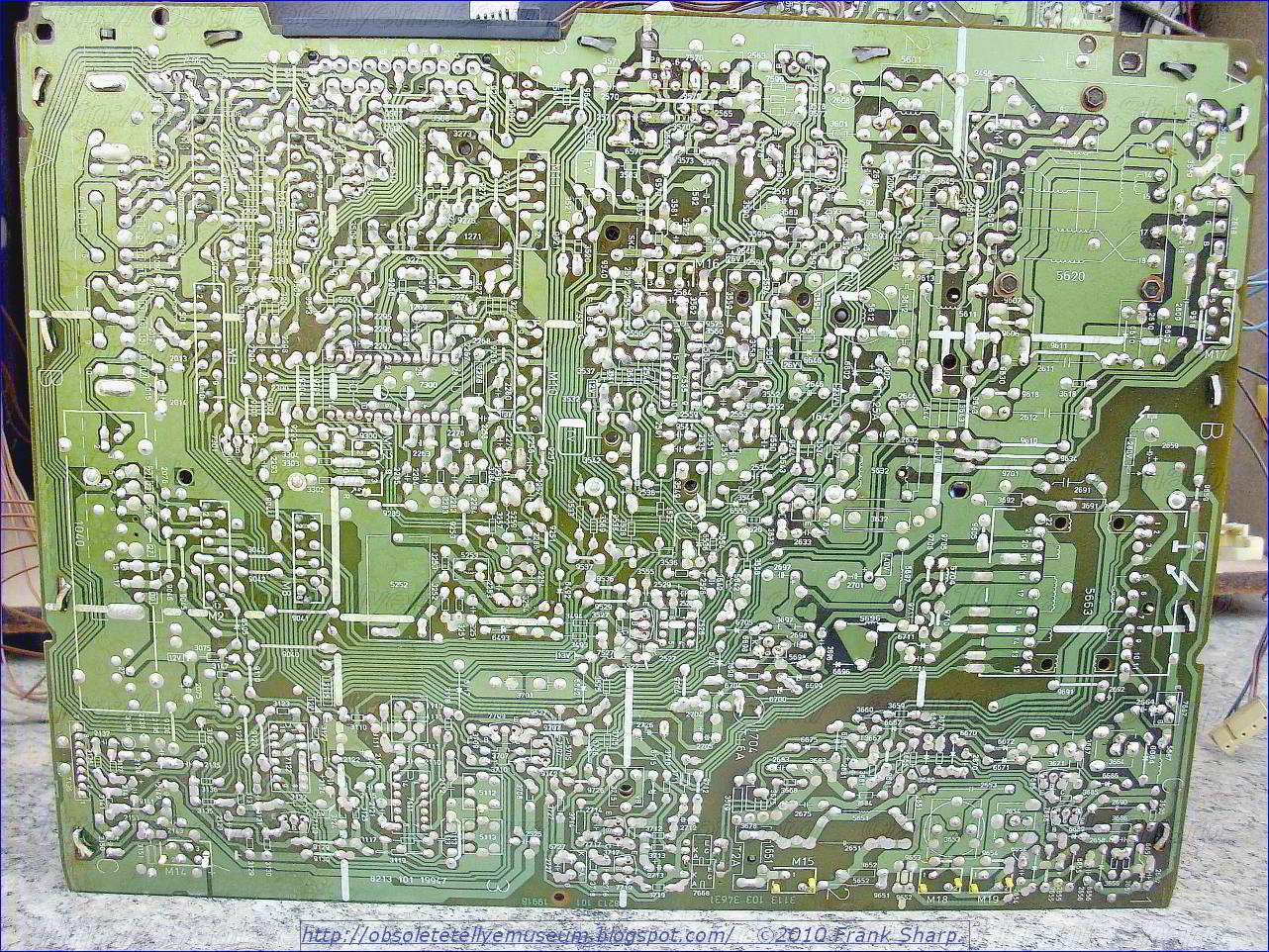
When I've seen for first time this chassis I had a laugh as like seeing a tv set with missing parts. The reality was indeed true no missing parts the chassis is the forerunner of the minimisation of tv chassis technology.


- POWER SUPPLY OPERATION In Brief :
The chopper circuit relies on feedback from the transformer to sustain oscillation. As with any chopper circuit, regulation is achieved by controlling the on/off timing of the chopper transistor. For control purposes the base of Tr7717 monitors the 140V h.t. supply. Its emitter is provided with a stable 6.2V reference voltage by zener diode D6715. The error voltage produced at the collector of Tr7717 drives Tr7719 which controls the current through the LED in the CNX62 optocoupler Tr7668. This device is used to provide mains isolation in the feedback path. The light-sensitive section of the optocoupler sets the d.c. voltage at the base of transistor Tr7685. At switch on the base of the chopper transistor Tr7687 is forward biased via R3686. It switches on and a sawtooth current flows through the primary winding 5-7 of the chopper transformer T5663. Tr7687 and T5663 form a blocking -oscillator circuit. Positive feedback via winding 1-9 on the transformer and D6672 drives Tr7687. When the transformer satu- rates, the drive is removed and Tr7687 switches off. The resonant circuit formed by C2664 with the primary winding of T5663 then oscillates, producing an overswing that switches Tr7687 on again. In normal operation Tr7687's switch -off timing is controlled by the pulse -width modulator consisting of transistor Tr7685 and its associated components. As mentioned above, the d.c. conditions at the base of Tr7685 are set by the conduction of the optocou- pler. The base of Tr7685 is also fed with a sawtooth L waveform that's developed across C2675, which with R3678/9 integrates the feedback from winding 1-11 on the transformer via D6667. In addition a negative reference voltage is established across C2690 by the action of D6689 and D6672 while Tr7687 is conductive. When the sawtooth waveform at the base of Tr7685 has risen to a sufficiently posi- tive value Tr7685 and Tr7686 switch on, removing the drive from Tr7687 which switches off very rapidly. The nominal operating frequency of the chopper circuit is 40kHz - it can vary between 20-60kHz. Over -voltage protection is provided by thyristor Ty6698 whose gate voltage is obtained from one of the rectifiers connected to the line output transformer. If the voltages in the line output stage are excessive Ty6698 conducts, placing a short-circuit across the 140V line. In this state the chopper circuit operates at a very low frequency of approximately 1.3kHz, with low voltage/current conditions. Current via D6696 holds Ty6698 on - switching the set off removes this short- circuit condition. In the unloaded state the circuit operating frequency is approximately 100Hz. In the standby mode thyristor Ty6727 is switched on to maintain the 5V supply to the control section without the need for a separate power supply. In this mode the control circuit provides drive to the anode of the optocoupler LED and the voltages delivered to rest of the set are far below the normal levels.
 Fig. 1 shows the circuit. The most common problem is failure of the BUT11 chopper transistor Tr7687. In this event the mains fuse F1651 will usually be blackened or even shattered, with possible failure of one or more of the bridge rectifier diodes D6654-7. The surge limiter resistor R3654 will sometimes have failed as well. Remove the faulty BUT11 transistor and check D6663, D6664 and C2664. This capacitor can split: use a good quality 1.5kV capacitor in this position. In later sets the snubber network D6663/R3663/C2663 may be omitted, in which case the chopper transistor is type BUT11A. It's important that the correct type of transistor is used in this position. A BUT11 fitted in a set without the snubber network will fail again, but it's perfectly in order to fit a BUT11A in all sets. Transistors Tr7685 and Tr7686 should also be checked and, we've learnt from experience, it's best to replace the CNX62 optocoupler Tr7668 in the error signal feedback circuit Once replacement components have been fitted as neces- sary there's an official modification that should be carried out on earlier sets to reduce the likelihood of chopper tran- sistor failure. It consists of fitting a BYD33D diode with its anode to the collector of transistor Tr7686 and its cathode to the base of the chopper transistor Tr7687, and reconnecting R3687 so that one end remains connected to the base of Tr7686 while the other end is moved to connect with the base of Tr7687.
 Before you switch on it's best to carry out a visual examination for dry -joints, particularly around the chopper trans- former T5663 and the mains input circuit, including the degaussing thermistor R3653. Dry -joints in these areas could have been the' cause of the original failure of the chopper transistor. I suggest that you then disconnect the supply to the line output stage by unplugging connector M17 and provide a dummy load in the form of a 60W lamp - connect it across the 140V h.t. supply's 47µF reservoir capacitor C2697. A meter set to read the h.t. voltage should also be connected here. Next connect the set to the mains supply via a variac which should be set to OV output. Switch on and slowly advance the output from the variac to about 90V. If all is well the lamp should by now be glowing and the meter should read about 140V. If the reading is low, at about 40V, the set may be in the standby condition (this applies to remote control sets). Try pressing the programme up or down button at the front of the set: this should bring it out of standby. If the supply now reads 140V, advance the setting of the variac SLOWLY, checking that the 140V supply remains 19V to audio Lc 220 220 12V 1k6 Tr7707 BC548 160 109621 constant. Should the h.t. voltage rise with the increased supply from the variac, switch off and check the circuit around the optocoupler. One possible cause of no regulation is broken print between R3659 and R3660.
If the h.t. supply remains low or doesn't come up at all, switch off and check the mains input circuitry and the 680kS2 start-up resistor R3686. One cause a failure to start is a defective degaussing thermistor (R3653) - it has two sections, one of which may provide surge limiting.
The correct replacement must be used - there are different types for 110° and 90° sets.
Engineers are often caught out by this, fitting the wrong type then spending hours trying to find out why the power supply won't work on load. Once the 140V supply has been established and is stable the variac can be brought up to provide the full mains supply. It should then be possible to switch off the set, disconnect the lamp and meter, reconnect socket M17 and check the set out. I've found this power supply repair procedure to be the safest way of ensuring that the minimum number of BUT11A transistors end up in the bin!
A faulty chopper transformer can cause repeated failure of the BUT11A transistor, but in my experience this is uncommon.
CHASSIS 2A The Line Output Stage:
Not many faults occur in the line output stage, which uses conventional circuitry. One point to note is that the line output transistor is type BU508V. A BU508A is not suitable and will fail within a very short time. Another common problem is failure of C2618. Its value depends on the screen size: the rating is 2kV. C2609, whose value is also dependent on screen size (voltage rating 2kV), can also be a problem. One case of line cramp at the right-hand side of the screen was caused by a defective line driver transformer. So far I've had to change the line output transformer in this chassis, but it does seem to suffer from dry -joints. These should be attended to as a matter of course. If, when the brightness setting is advanced, you have a blank raster with flyback lines check C2496 (22nF). When this capacitor goes open -circuit the luminance amplifier in the colour decoder chip is biased off. It's part of the beam limiting circuit. Timebase Generators The sync circuitry and timebase generators are contained within the well-known TDA2579 chip IC7535, which also provides sandcastle pulse and transmission identification outputs. No line drive with the h.t. supply present should lead to a check at pin 16 of this chip. This pin receives a start-up supply from the chopper circuit via R3556 (2700) and 83555 (5600) - during normal operation the chip is operated from a line output stage derived 11V line (+13a). The voltage is stabilised at 9V within the chip. If the voltage at pin 16 is low, check whether the external zener diode D6555 (BZX79/C12) is leaky or short-circuit. The chip itself could be faulty. If
removing the solder from pin 16 makes the 9V supply come up, replace the chip. Field Output The field output stage consists of a TDA3653 chip in 20 and 21in. models or a TDA3654 in larger -screen sets. The most common fault is for the chip to have failed. Wheneveryou have to fit a replacement, C2571 (100µF) and C2565 (390pF) must also be changed. Failure of these two capaci- tors can result in failure of the chip. C2565 is a small, plate - ceramic capacitor that's mounted on the print side of the board, between pins 1 and 5 of the i.c. If it's left out, a herringbone -type pattern may be seen on the screen followed by the rapid demise of the chip.
CHASSIS 2A Audio Stages:
The audio output chip is a TDA1013A. No problems here apart from occasional failure of the chip itself. Another possible cause of no sound is the headphone socket. The well-known TBA120S intercarrier sound chip is used (IC7111), with the interstation mute voltage being applied to pin 4. Between these two chips there's an HEF4053BP i.c. (IC7122) for switching between internal or external audio, the latter being fed via the scart socket. This chip has been known to fail, giving the no sound symptom: as a quick check pins 13 and 15 can be shorted together so. that the off -air sound is fed directly to the audio chip.
CHASSIS 2A Video Section:
A TDA3561A colour decoder chip is used. No colour or no luminance can be caused by the chip itself. With no luminance however first check the voltage at the contrast control pin 7. If the voltage here is nbgative or very low and not controllable, you might fmd that the trouble is caused by the previously mentioned capacitor C2496 in the line output stage. Failure of the 8.867MHz crystal X1269 is an occa- sional cause of no colour.
The only problems I've had with the c.r.t. base panel mounted RGB output stages have been dryjoints, giving intermittent colours.
CHASSIS 2A Tuner and IF Circuits; The tuner is normally a U343C or U344C depending on whether the set has remote control. It's understood that these have been superseded by later versions and that no modifications are required when fitting one of these as a replacement. The i.f. module U1040 is not considered to be a repairable unit. If the can is opened however you find that there's a standard TDA2541 chip and a SAW filter. I.F. problems are usually caused by the chip itself, which can be replaced.
There's a single transistor in the can, Tr7065 (BC548). It's the video emitter -follower.
The video signal leaves the i.f. can at pin 15, passing to the TDA5850 chip IC7526 which switches between internal and external video. This chip can fail, the result being loss of video signal. Make sure that the set hasn't been switched to external video via the remote control unit however!
CHASSIS 2A Teletext: A strange "net -curtain" effect can sometimes be seen on the screen with teletext models. It takes the form of fairly close, evenly -spaced faint bars that run from the top to the bottom of the screen.
The cause is the SAA5241 chip IC7770 on the teletext panel going high -resistance in its socket. To cure the trouble remove the chip and its holder then solder the chip into the board directly. Apart from this the teletext panel is very reliable. Odd dropouts can some- times be cured by careful adjustment of the 6MHz oscillator (trim C2802).
CHASSIS 2A Control Section: Few
faults occur in the control section. I've had stuck buttons on the control panel (Telefunken strip PCB), giving continuous programme changing etc. The most common problem is loss of memory due to failure of the nicad backup battery. When this has to be replaced the set must be retuned and the personal prefer- ence levels reset. Another occasional problem is failure to come out of the standby mode. If it's not due to the nicad battery, check that the BZX79/C4V7 zener diode D6734 isn't leaky. Conclusion It's hoped that these notes will be of help to engineers who are not too familiar with the 2A chassis. Notes on some later Philips chassis will follow in subsequent posts. Since the SOPS power supply circuit was used in several chassis (Born on K40) the notes on this in the present article also apply to the other related chassis.
1. A degaussing circuit for demagnetizing ferromagnetic components in a colour television receiver, said circuit comprising a rectifier circuit, the series arrangement of a degaussing coil and a first thermistor with a positive temperature coefficient, said series arrangement is connectable to at least one terminal of an alternating current voltage source, and furthermore comprising a resistance element means for contributing to heating of the first thermistor and for protecting said rectifier circuit comprising a second thermistor with a negative temperature coefficient which is connectable to a terminal of the alternating current voltage source and which is thermally coupled to the first thermistor with a positive temperature coefficient, the second thermistor being connected to said rectifier circuit in the receiver.
2. A circuit as claimed in claim 1, wherein said rectifier circuit comprises a rectifier having a current which also flows through the second thermistor, and the temperature of the second thermistor in the final operating state exceeds the temperature of the first thermistor.
3. A circuit as claimed in claim 2, wherein the second thermistor is connected in series with the rectifier circuit, the series arrangement thus formed being connected in parallel with the series arrangement of the degaussing coil and the first thermistor, and both series arrangements being connectable to the terminals of the alternating current voltage source.
4. A circuit as claimed in claim 2, wherein the series arrangement of the degaussing coil and the first thermistor is connected in parallel with the rectifier circuit, thereby forming two juctions, one of the junctions being connectable to a first terminal of the alternating current voltage source, the other juction being connected to the second thermistor, said second thermistor being connectable to the second terminal of the alternating current voltage source.
5. A circuit as claimed in claim 4, wherein the rectifier circuit comprises the Graetz type and a supply capacitor, and the product of the total ohmic resistance value of said parallel circuit in the cold state by the capacitance of said supply capacitor amounts to approximately 50% of the duration of the cycle of the voltage supplied by the alternating current voltage source.
6. A circuit as claimed in claim 2, wherein the second thermistor is connected in parallel with the series arrangement of the degaussing coil and the third thermistor, thereby forming a parallel circuit included in a supply lead of the rectifier, said rectifier comprising a full-wave rectifier of the type that substantially no direct current component can flow through said supply lead.
7. A circuit as claimed in claim 6, wherein the resistance value of the first thermistor in the cold state is more than 20 times lower than the ohmic resistance value of the degaussing coil.
8. A circuit as claimed in claim 6, characterized in that the rectifier circuit is of the Graetz-type and in that the product of the total ohmic resistance value of the said parallel circuit in the cold state by the capacitance of a supply capacitor being part of the rectifier circuit amounts to approximately 50% of the duration of the cycle of the voltage supplied by the a.c. voltage source.
9. A circuit as claimed in claim 6 wherein the rectifier circuit comprises the Graetz type.
Description:
The invention relates to a degaussing circuit for demagnetizing ferromagnetic components in a colour television receiver, comprising the series arrangement of a degaussing coil and a thermistor with a positive temperature coefficient, which series arrangement is connectable to at least one terminal of an a.c. voltage source and furthermore comprising a resistance element for contributing to heating of the thermistor.
Such a circuit is known from German Patent Specification No. 1,282,679. In order to reduce the current which flows through the degaussing coil at the end of the process, which current might produce an unwanted magnetic residual field in the ferromagnetic components to be demagnetized the thermistor is raised by means of a resistance element already present in the receiver to a higher temperature than the temperature which would be produced by the final current alone. For this results in a further increase in the resistance value of the thermistor.
In practice, in the known circuit a wire-wound resistor with a high permissible power can be used as resistance element, which wire-wound resistor is arranged in the immediate vicinity of the thermistor. However, the drawback of this measure is that the temperature of the wire-wound resistor cannot be controlled so very well so that the difference between the maximum permissible temperature of the thermistor and the ambient temperature cannot be checked with certainty. Consequently, the risk of overheating, which may be destructive to the thermistor, is not excluded. For this reason the circuit is no longer used.
It is an object of the invention to avoid said drawback of the known circuit whilst also the costs can be reduced and to that end the circuit according to the invention is characterized in that the resistance element is a (second) thermistor with a negative temperature coefficient which is connectable to a terminal of the a.c. voltage source and which is thermally coupled to the (first) thermistor with a positive temperature coefficient, the second thermistor being at the same time a protection resistance for a rectifier circuit in the receiver.
By means of heat transfer from the second to the first thermistor the latter attains, as wanted, a higher temperature. As the current through the second thermistor soon assumes a value which substantially does not depend on the degaussing circuit and which cannot exceed a given maximum, an equilibrium condition is obtained whereafter the temperature cannot increase to an appreciable extent so that the circuit according to the invention is safe. It will be noted that degaussing circuits having two thermally intercoupled thermistors having temperature coefficients of the opposite sign are known per se. U.S. Pat. No. 3,495,136 discloses a circuit which includes such a combination. The publication "IEEE Transactions on Broadcast and Television Receivers" Vol. BTR 1972, No. 1, pages 7 to 9 inclusive describes degaussing circuits in which a thermistor having a negative temperature coefficient is included in series with a supply voltage circuit. However, this thermistor is not thermally coupled to a thermistor having a positive temperature coefficient.
The invention will be further explained by way of non-limitative example with reference to the accompanying figures wherein
FIG. 1 shows a first construction of the circuit according to the invention,
FIG. 2 is a characteristic curve for explaining the invention,
FIG. 3 shows a second construction of the circuit according to the invention,
FIG. 4 shows a third construction of the circuit according to the invention,
FIGS. 5a and 5b are waveforms occurring therein and
FIG. 6 shows a fourth construction of the circuit according to the invention.

In FIG. 1 a degaussing coil 1 of a partly shown colour television receiver having a display tube of the shadow mask type is in series with a thermistor 2. The series arrangement of a second thermistor 7 and a rectifier circuit 8 is in parallel with the series arrangement of coil 1 and thermistor 2. Thermistor 7 has a negative temperature coefficient, whilst thermistor 2 has a positive temperature coefficient. The thermistors are thermally coupled because they have been brought into intimate contact with one another which is indicated in FIG. 1 by means of a double arrow. The parallel circuit constituted by components 1, 2, 7 and 8 can be connected through a switch 6 to the terminals 3 and 4 of an A.C. voltage source 5, for example the electric power supply mains.
Rectifier circuit 8 is diagrammatically shown in FIG. 1 as the series arrangement of a rectifier 9 and the parallel arrangements of a supply capacitor 10 of a high capacitance and a load 11. In operation the rectifier 9, which may consist in known manner of one or more diodes, rectifies the mains voltage of source 5 so that a D.C. voltage is available across capacitor 10 for feeding further parts of the receiver. A direct current flows through these parts. So load 11 represents a resistance whose value is equal to the ratio of said d.c. voltage to this direct current. Of course the receiver may comprise further supply circuits, not shown, for example for generating D.C. voltages of different values as well as one or more mains transformers.
In the cold condition thermistor 2 has a comparatively low resistance value (of approximately 25 Ohm), whilst thermistor 7 has a comparatively high value (of approximately 70 Ohm). Immediately after switch-on of mains switch 6 a large current flows through the thermistor 2 and coil 1 of approximately 5 A (peak value) or more. Because the series arrangement of the thermistor 7 and rectifier circuit 8 is in parallel with the source 5 the current therethrough is at the start independent of the degaussing current which flows through the branch 1, 2. The currents through both thermistors are able to heat them in a rather short time (approximately 10 seconds).
FIG. 2 shows on a logarithmic scale the resistance value R of thermistor 2 plotted as a function of the temperature T. Above the so-called Curie-temperature To (approximately 75° C.) the specific resistance of the material from which the thermistor 2 consists and consequently also its resistance value increases very steeply. In the absence of thermistor 7 thermistor 2 would attain, owing to self-heating, a temperature T1 (approximately 130° C.) with a corresponding resistance value R1 of approximately 20 kOhm, the amplitude of the degaussing current would then be brought to a value of approximately 20 mA.

When the temperature increases the resistance value of thermistor 7 decreases. The current through this thermistor is mainly determined by the values of the voltage across and of the current through load 11, which values, in the warm condition, are substantially independent of the temperature of thermistors 2 and 7 and of the degaussing circuit. For, they only depend on the operating conditions of the various parts of the receiver which are provided with supply voltage by circuit 8. Said current cannot, for example owing to the action of a safety circuit, exceed a given maximum.
The final value of thermistor 7 is low, for example, approximately 1 Ohm and a current of 1.5 A (r.m.s. value) and a temperature of 175° C. Thermistor 7 is chosen such that even for the smallest possible current through it, depending on load 11, it attains a final temperature which is higher than T1. Consequently, thermistor 7 delivers heat to thermistor 2. As a portion of the heat radiated by the thermistor 7 yet goes to the environment the final temperature of thermistor 2 will be lower than that of thermistor 7. Owing to the heat transfer thermistor 7 attains a final temperature T2 which is approximately 20° to 30° C. higher than T1. An equilibrium condition occurs wherein the final temperature of thermistor 7 is lower than the final temparature without thermal coupling to thermistor 2 and wherein both thermistors are approximately kept at said final temperatures by the final currents. This situation is stable and, consequently, safe: for an increase in temperature T1 causes a decrease in the current through thermistor 2 which opposes the increase in the temperature. It also prevents the temperature from rising too high which might cause the resistance value R to decrease. The final value R2 of thermistor 2 is higher than R1, namely approximately 60 kOhm and the final amplitude of the current through coil 1 is reduced to the desired value, i.e. less than 5 mA.
In the preceding the dissipation in coil 1 in the final condition is assumed to be negligibly small with respect to that in thermistor 2. This is justified by the fact that the ohmic resistance value (approximately 20 Ohm) of coil 1 is much lower than value R2 so that the output voltage drop across coil 1 is negligibly small.
Thermistor 7 is a safety resistor for rectifier circuit 8. Because prior to switch-on of mains switch 6 capacitor 10 is still uncharged a very large current would flow through rectifier 9 and capacitor 10 after switch-on if thermistor 7 would be absent. This might cause damage to these components and also to switch 6. It would also be possible that a fuse 12 which in FIG. 1 is included between switch 6 and the junction point of thermistors 2 and 7 would melt. The starting current is limited by thermistor 7 whilst the thermistor substantially produces no voltage drop in the hot condition.
Compared with the case wherein thermistor 7 is replaced by a linear resistor the circuit according to the invention means a considerable saving in energy. For, the final value of thermistor 7 is lower than the value of the linear resistance i.e. the above-mentioned starting value (approximately 70 Ohm) of thermistor 7 whereas the value of the rectified voltage across capacitor 10 is only decreased during the warming up time of thermistor 7.
There is an additional advantage, namely the fact that after switch-on of mains switch 6 the current derived by circuit 8 from source 5 grows gradually and not suddenly which attenuates the jump produced by circuit 1, 2.
FIG. 3 shows a second construction of the circuit according to the invention, with the same reference numerals as in FIG. 1 wherein the rectifier circuit 8 is in parallel with the series arrangement of coil 1 and thermistor 2, whilst thermistor 7 is included between mains switch 6 and the junction of thermistor 2 and circuit 8. In this construction thermistor 7 limits the switch-on value also for the degaussing current so that for both thermistors types must be chosen which each have a lower starting value than in the case of FIG. 1. In the final state there is substantially no difference between the two constructions.
It will be noted that in the two described constructions of the circuit thermistor 7 has a dual function, namely protecting the rectifier circuit 8 and increasing the final value of thermistor 2 and, consequently, reducing the final degaussing current, which means a saving compared with the case where the degaussing circuit is constructed in a known manner, for example with two thermally inter-coupled thermistors with positive temperature-coefficients, whilst thermistor 7 or a linear resistor in the same position is not coupled herewith.
In FIG. 4 thermistor 7 is in parallel with the series arrangement of degaussing coil 1 and thermistor 2. The circuit constituted by components 1, 2 and 7 can be connected through fuse 12 and switch 6 to terminal 3 of a.c. voltage source 5. In this example rectifier 9 is of the Graetz-type: four diodes 9a, 9b, 9c and 9d form a bridge in a diagonal whereof components 10 and 11 are included, whilst a point of the other diagonal is connected to that junction of series arrangement 1, 2 and thermistor 7 which is not connected to mains switch 6. The other point of said diagonal is connectable through switch 6 to the other terminal 4 of source 5.In the cold state thermistor 2 has a comparatively low resistance value (of approximately 4 Ohm), whereas thermistor 7 has a comparatively high value (of approximately 150 Ohm). Capacitor 10 has as yet no charge. In this circuit coil 1 has an ohmic resistance value of approximately 100 Ohm. Immediately after switch-on of mains switch 6, the voltage of the source 5 is substantially completely across the parallel circuit constituted by components 1, 2, 7. If this voltage has an effective value of 220 V then a current of approximately 3.1 A (peak value) flows through thermistor 2 and coil 1, whilst a current of approximately 2.1 A flows through thermistor 7 which in the beginning is independent of the degaussing current flowing through branch 1, 2.
FIG. 5a represents one cycle of the current which flows through rectifier 9, at the start of the procedure. Herein it is assumed that the frequency of the mains voltage is 50 Hz which corresponds to a cycle of 20 ms. When capacitor 10 is discharged diodes 9a and 9d or 9b and 9c respectively conduct during the entire half cycle, that is to say that opening angle thereof is equal to 10 ms.
After switch-on the degaussing current through coil 1 gradually decreases, on the one hand, because the resistance value of thermistor 2 becomes higher when the thermistor becomes warmer and on the other hand because capacitor 10 is being charged. In addition, when the temperature increases the resistance value of thermistor 7 decreases. The final value thereof is low, for example approximately 2 Ohm. As in FIG. 1 and 3, thermistor 2 attains a final temperature T2 which exceeds the final temperature T1 which would be attained by self-heating in the absence of thermistor 7, which causes the final valve of thermistor 2 to become higher. The final amplitude of the degaussing current is consequently reduced to the desired value. This final state is stable and, consequently, safe.
FIG. 5b represents one cycle of the current flowing through rectifier 9 at the end of the process. The value thereof depends on the value of load 11; in a given receiver a peak value of approximately 4A was measured at an opening angle for the rectifying diodes of approximately 3 ms. It will be noted that the degaussing current through coil 1 is substantially of the same form as the currents in FIG. 5a and 5b as the reactance of the coil at low frequencies may be neglected relative to the ohmic resistance value hereof. FIGS. 5a and 5b show that the shape of the current is substantially symmetrical relative to the zero value. A condition for this is that the decrease in the amplitude of the degaussing current does not take place too rapidly, which decrease is determined by the product of the resistance value of the circuit 1, 2, 7 and the capacitance of capacitor 10. Because the capacitance is determined by the permissible amplitude of the ripple voltage across load 11 said condition implies a minimum value for this resistance and, consequently, of the initial resistance value of thermistor 7 and of the ohmic resistance value of the degaussing coil, whilst maintaining the magnetic properties thereof. In the example of FIG. 4 capacitor 10 has a capacitance of 200 μuF whilst said resistance value is approximately 60 Ohm in the cold state so that said product is approximately equal to 12 ms, that is to say in the order of magnitude of 50 to 60 % of the duration of the cycle.

The reason why the shape of the current must be substantial symmetrical relative to the zero value, the negative and the positive peak values being consequently substantially equal to one another, is that the degaussing current should substantially not contain a direct current component, which component would generate an unwanted magnetic field. When using a Graetz-rectifier as is the case in FIG. 4, the degaussing current reverses its direction at each half cycle as the current alternatingly flows either through diodes 9b and 9c or through diodes 9d and 9a. A single-phase rectifier in which the current does not reverse may not be used for the construction of FIG. 4. FIG. 6 represents a rectifier of the voltage doubler type which may be used. Herein rectifier circuit 8 comprises two diodes 9a and 9b and two capacitors 10a and 10b. It is obvious that the degaussing current which also flows through capacitor 10b comprises no direct current component. It is also obvious that the circuit 1, 2, 7 may be included in the supply lead to terminal 4 which, of course, also applies to the construction in FIG. 4. It can be noted that the single-phase rectifier, shown in FIG. 3, produces a d.c. voltage drop across thermistor 7. Consequently, also in this construction, reference should be given a Graetz rectifier.
In FIGS. 4 and 6 the initial current is limited by components 1, 2 and, especially, 7. It will be noted that thermistor 2 always has a rather low voltage drop across it, both in FIG. 4 and in FIG. 6. For, at the beginning of the process the voltage of source 5 is found substantially fully across coil, 1, which has a much higher ohmic resistance value, whilst the voltage across the series circuit 1, 2 at the end of the process is low, as thermistor 7 which is now low-ohmic substantially short-circuits said series arrangement. The advantage thereof is that thermistor 2 may be much thinner than thermistor 2 in FIGS. 1 and 3, that is to say 0.5 to 0.7 mm instead of approximately 2 mm, which means a considerable saving in material. It is consequently cheaper. In addition, the dissipation is much lower and the loss of heat to the environment much lower. The preceding also applies with respect of thermistors which in known circuits are in series with the degaussing coil and which, at least at the beginning of degaussing must be able to withstand a high voltage.
PHILIPS 26CE2281 RUBENS CHASSIS 2A Composite thermistor component:
A component consisting of two coupled PTC thermistors with the first thermistor having a lower cold resistance than the second thermistor and the first thermistor having a higher resistance at the operating temperature than the second thermistor. According to the invention, the electric connection to the second thermistor is made directly by solely mechanical contacts to the surface of the ceramic thermistor body. This means a considerable simplification during manufacture, as the second thermistor need not be provided with electrode layers.
Inventors:
Belhomme, Charles J. G. (Brussels, BE) U.S. Philips Corporation (New York, NY)
1. A thermistor component comprising
a first positive temperature coefficient of resistance thermistor,
a second positive temperature coefficient of resistance thermistor thermally in contact with said first thermistor, said second thermistor having a resistance substantially higher than the resistance of said first thermistor in the unoperated condition, and said second thermistor having a resistance lower than the resistance of the first thermistor at an operating temperature, wherein said second thermistor contributes to heating of said first thermistor during operation,
electrical connection to said first thermistor applied through metallic contact layers on said first thermistor, and
electrical connection to said second thermistor applied solely by mechanical contacts to a surface of said second thermistor, wherein said first thermistor has contact layers at opposite major faces, and said second thermistor has opposite major faces free of contact layers.
2. A degaussing circuit having a thermistor component as claimed in claim 1, in which said first thermistor is connected in a series arrangement with a degaussing coil and an alternating mains supply, and said second thermistor is connected in parallel with said series arrangement.
3. A thermistor component comprising
a first positive temperature coefficient of resistance thermistor,
a second positive temperature coefficient of resistance thermistor thermally in contact with said first thermistor, said second thermistor having a resistance substantially higher than the resistance of said first thermistor in the unoperated condition, and said second thermistor having a resistance lower than the resistance of the first thermistor at an operating temperature, wherein said second thermistor contributes to heating of said first thermistor during operation,
electrical connection to said first thermistor applied through metallic contact layers on said first thermistor, and
electrical connection to said second thermistor applied solely by mechanical contacts to a surface of said second thermistor, wherein said mechanical contacts include contact springs in direct contact with a major face of said second thermistor, and wherein at least one of said contact springs is in contact with a contact layer on said first thermistor.
4. A thermistor component comprising
a first positive temperature coefficient of resistance thermistor,
a second positive temperature coefficient of resistance thermistor thermally in contact with said first thermistor, said second thermistor having a resistance substantially higher than the resistance of said first thermistor in the unoperated condition, and said second thermistor having a resistance lower than the resistance of the first thermistor at an operating temperature, wherein said second thermistor contributes to heating of said first thermistor during operation,
electrical connection to said first thermistor applied through metallic contact layers on said first thermistor, and
electrical connection to said second thermistor applied solely be mechanical contacts to a surface of said second thermistor, wherein said first and second thermistors each have a major face in contact with a feedthrough plate, wherein said mechanical contacts include contact springs in direct contact with a major face of said second thermistor, and wherein at least one of said contact springs is in contact with a contact layer on said first thermistor.
5. A thermistor component according to claim 1, wherein said first and second thermistors are ceramic.
6. A thermistor component according to claim 1, wherein said first thermistor has a Curie point of 75° C. and said second thermistor has a Curie point of 180° C.
7. A thermistor component comprising
a first positive temperature coefficient of resistance thermistor,
a second positive temperature coefficient of resistance thermistor thermally in contact with said first thermistor, said second thermistor having a resistance substantially higher than the resistance of said first thermistor in the unoperated condition, and said second thermistor having a resistance lower than the resistance of the first thermistor at an operating temperature, wherein said second thermistor contributes to heating of said first thermistor during operation,
electrical connection to said first thermistor applied through metallic contact layers on said first thermistor, and
electrical connection to said second thermistor applied solely by mechanical contacts to a surface of said second thermistor, wherein said first and second thermistors each have a major face in contact with a feedthrough plate, and wherein said first thermistor has contact layers at opposite major faces, and said second thermistor has opposite major faces free of contact layers.
Description:
The invention relates to a composite thermistor component comprising two thermistors having a positive temperature coefficient of the resistance, the thermistors being thermally coupled to one another, to a degaussing circuit in which the component is incorporated and to colour television receiver comprising a shadow-mask picture display tube and a degaussing circuit of this type.
Such a composite thermistor component, which is described in United Kingdom patent specification No. 1,531,277 comprises a first thermistor and a second thermistor which each have a positive temperature coefficient of resistance, the second thermistor having a resistance which is substantially higher than the resistance of the first thermistor when the thermistors are in the unoperated (cold) condition, the two thermistors being thermally coupled such that in operation the second thermistor contributes to the heating of the first thermistor and that the resistance of the second thermistor at the final operating temperature of the component is lower than the resistance of the first thermistor.
It is an object of the invention to considerably simplify the composite thermistor component and according to the invention it is characterized in that the electrical connection to the second thermistor is made directly by solely mechanical contacts to the surface of the ceramic thermistor body.
The present invention will be described without limitation by reference to the drawing figures wherein
FIG. 1 is a schematic representation of a circuit used for degaussing metal parts, and
FIG. 2 is a view of a structure in accordance with the present invention.
The composite thermistor component is inter alia used in a circuit for degaussing metal parts, particularly the inner shield and the shadow mask, of a colour television display tube. A first thermistor 2 is connected in a series arrangement with a degaussing coil 1 to a first (3) and second (4) terminal for an alternating mains supply (5) via a switch (6), the first thermistor having a positive temperature coefficient of resistance, and the second thermistor 7 has a positive temperature coefficient of resistance connected in parallel with the series arrangement of coil 1 and thermistor 2. The two thermistors are thermally coupled because they are in intimate contact with one another.

This is shown in FIG. 1 by means of an arrow.
The description and the drawing of the abovementioned United Kingdom patent specification give the impression that the two thermistors are contacted directly by means of the ceramic surfaces. For a person skilled in the art, the use of ceramic components having metallized areas of contact in an electrical circuit has, however, always been such a matter of course that the presence of such metallized areas of contact had been omitted from the description for the sake of simplicity.
As a matter of fact, contacting by way of the ceramic surface by mechanical contact only can only be effected on the parallel thermistor in the circuit, that is to say the thermistor which, in the unoperated condition, has the higher resistance, contributes to heating the other thermistor during operation and has at the prevailing temperature a resistance which is lower than that of the other thermistor.
The thermistor which is in series with the degaussing coil must be of a low resistance during the unoperated condition and the metallized layer which is in intimate contact therewith must be present on substantially the entire surface area. Contacting of the series thermistor body by solely mechanical contacts only directly to the surface of the thermistor body does not result in a useful component.
Relative to the component which is known from the United Kingdom patent specification No. 1,531,277, in which the second thermistor (7) is provided with a vacuum-deposited nickel-chromium nickel-chromium layer onto which a thin silver layer has been vacuum-deposited, which silver layer is reinforced with a silver paste, the second thermistor must be somewhat changed to obtain a composite component according to the invention having similar operating characteristics. The material must have a Curie point which is approximately 10° C. higher than that of the material used for the second thermistor in the United Kingdom patent specification No. 1,531,277 component in order to achieve this.
In FIG. 2, reference numerals 2 and 7 denote the thermistors which have been given the same reference numerals as in FIG. 1, that is to say 7 is the thermistor having a positive temperature coefficient and a resistance value which is higher than that of thermistor 2 when the thermistors are in the unoperated (cold) condition and a resistance value at the final operating temperature which is lower than the resistance value of thermistor 2.
Thermistor 2 is provided on each major surface by vacuum deposition with a 0.1 μm thick Ni-Cr layer, onto which a 0.3 μm thick silver layer and a 10 μm silver containing layer are deposited, the three superposed layers constituting a contact layer 11. Thermistor 7 is built-in without having been provided with a contact layer on either major surface. In the composite thermistor component, the major surface of the thermistor 7 which is opposed to the thermistor 2 bears directly against a silver-plated stainless steel plate 12, which is provided with a feed-through 9 to the circuit, and the silver-plated stainless plate 12 bears against the contact layer 11 on the opposed major surface of the thermistor 2. On both sides the silver-plated stainless steel contact springs 8 and 10 push against the thermistors, that is to say contact spring 8 is in direct contact with the ceramic surface of thermistor 7 and contact spring 10 is in direct contact with the contact layer 11 on thermistor 2.
In one embodiment thermistor 2 has a composition
Ba0,80 Ca0,10 Sr0,10 TiO3 +0,3 mole % TiO2 +0,4 mole % Sb2 O3 and 0,08 mole % MnO.
This thermistor has a resistance value of approximately 40 Ohm at 25° C., the Curie point being 75° C.
Thermistor 7 has the composition:
B0,70 Ca0,10 Pb0,20 TiO3 +3 mol % TiO2 +0,4 mol % Sb2 O3 +0,08 mol % MnO.
This material has a Curie point of 180° C. The resistance value of the thermistor at 25° C. was not determined without contact layers, which is difficult to achieve, but with vacuum-deposited contact layers, a resistance of 50 to 400 Ohm then been measured.
In the construction of the thermistor as described in United Kingdom patent specification No. 1,531,277, provided with vacuum-deposited NiCr+Ag and a silver-containing layer, material was used having a Curie point of 170° C. and a resistance of the thermistor at 25° C. of 800-4000 Ohm. The relevant composition was:
Ba0,72 Ca0,10 Pb0,18 TiO3 +0,3 mol % TiO2 +0,4 mole % Sb2 O3 +0,08 mole % MnO.
Chrominance + Luminance with TDA3561A,
GENERAL DESCRIPTION
The TDA3561A is a dec
and demodulation of PAL signals. Furthermore it contains a luminance amplifier, an RGB-matrix and amplifier. These
amplifiers supply output signals up to 5 V peak-to-peak (picture information) enabling direct drive of the discrete output
stages. The circuit also contains separate inputs for data insertion, analogue as well as digital, which can be used for
text display systems (e.g. (Teletext/broadcast antiope), channel number display, etc. Additional to the TDA3560, the
circuit includes the following features:
· The peak white limiter is only active during the time that the 9,3 V level at the output is exceeded. The start of the limiting function is delayed by one line period. This avoids peak white limiting by test patterns which have abrupt
transitions from colour to white signals.
· The brightness control is obtained by inserting a variable pulse in the luminance channel. Therefore the ratio of
brightness variation and signal amplitude at the three outputs will be identical and independent of the difference in gain
of the three channels. Thus discolouring due to adjustment of contrast and brightness is avoided.
· Improved suppression of the internal RGB signals when the device is switched to external signals, and vice versa.
· Non-synchronized external RGB signals do not disturb the black level of the internal signals.
· Improved suppression of the residual 4,4 MHz signal in the RGB output stages.
· Cascoded stages in the demodulators and burst phase detector minimize the radiation of the colour demodulator
inputs.
· High current capability of the RGB outputs and the chrominance output.
The function is described against the corresponding pin
number.
1. + 12 V power supply
The circuit gives good operation in a supply voltage range
between 8 and 13,2 V provided that the supply voltage for
the controls is equal to the supply voltage for the
TDA3561A. All signal and control levels have a linear
dependency on the supply voltage. The current taken by
the device at 12 V is typically 85 mA. It is linearly
dependent on the supply voltage.
2. Control voltage for identification
correct operation. The voltages available under various
signal conditions are given in the specification.
3. Chrominance input
The chroma signal must be a.c.-coupled to the input.
Its amplitude must be between 55 mV and 1100 mV
peak-to-peak (25 mV to 500 mV peak-to-peak burst
signal). All figures for the chroma signals are based on a
colour bar signal with 75% saturation, that is the
burst-to-chroma ratio of the input signal is 1 : 2,25.
4. Reference voltage A.C.C. detector
This pin must be decoupled by a capacitor of about 330
nF. The voltage at this pin is 4,9 V.
5. Control voltage A.C.C.
The A.C.C. is obtained by synchronous detection of the
burst signal followed by a peak detector. A good noise
immunity is obtained in this way and an increase of the
colour for weak input signals is prevented. The
recommended capacitor value at this pin is 2,2 mF.
6. Saturation control
The saturation control range is in excess of 50 dB.
The control voltage range is 2 to 4 V. Saturation control is
a linear function of the control voltage.
When the colour killer is active, the saturation control
voltage is reduced to a low level if the resistance of the
external saturation control network is sufficiently high.
Then the chroma amplifier supplies no signal to the
demodulator. Colour switch-on can be delayed by proper
choice of the time constant for the saturation control
setting circuit.
When the saturation control pin is connected to the power
supply the colour killer circuit is overruled so that the colour
signal is visible on the screen. In this way it is possible to
adjust the oscillator frequency without using a frequency
counter (see also pins 25 and 26).
7. Contrast control
The contrast control range is 20 dB for a control voltage
change from + 2 to + 4 V. Contrast control is a linear
function of the control voltage. The output signal is
suppressed when the control voltage is 1 V or less. If one
or more output signals surpasses the level of 9 V the peak
white limiter circuit becomes active and reduces the output
signals via the contrast control by discharging C2 via an
internal current sink.
8. Sandcastle and field blanking input
The output signals are blanked if the amplitude of the input
pulse is between 2 and 6,5 V. The burst gate and clamping
circuits are activated if the input pulse exceeds a level of
7,5 V.
The higher part of the sandcastle pulse should start just
after the sync pulse to prevent clamping of video signal on
the sync pulse. The width should be about 4 ms for proper
A.C.C. operation.
9. Video-data switching
an input pulse between 1 V and 2 V. In that condition, the
internal RGB signals are switched off and the inserted
signals are supplied to the output amplifiers. If only normal
operation is wanted this pin should be connected to the
negative supply. The switching times are very short
(< 20 ns) to avoid coloured edges of the inserted signals
on the screen.
10. Luminance signal input
The input signal should have a peak-to-peak amplitude of
0,45 V (peak white to sync) to obtain a black-white output
signal to 5 V at nominal contrast. It must be a.c.-coupled to
the input by a capacitor of about 22 nF. The signal is
clamped at the input to an internal reference voltage.
A 1 kW luminance delay line can be applied because the
luminance input impedance is made very high.
Consequently the charging and discharging currents of the
coupling capacitor are very small and do not influence the
signal level at the input noticeably. Additionally the
coupling capacitor value may be small.
11. Brightness control
The black level of the RGB outputs can be set by the
voltage on this pin (see Fig.5). The black level can be set
higher than 4 V however the available output signal
amplitude is reduced (see pin 7). Brightness control also
operates on the black level of the inserted signals.
12, 14, 16. RGB outputs
The output circuits for red, green and blue are identical.
Output signals are 5,25 V (R, G and B) at nominal input
signals and control settings. The black levels of the three
outputs have the same value. The blanking level at the
outputs is 2,1 V. The peak white level is limited to 9,3 V.
When this level exceeded the output signal amplitude is
reduced via the contrast control (see pin 7).
13, 15, 17. Inputs for external RGB signals
The external signals must be a.c.-coupled to the inputs via
a coupling capacitor of about 100 nF. Source impedance
should not exceed 150 W. The input signal required for
a 5 V peak-to-peak output signal is 1 V peak-to-peak.
At the RGB outputs the black level of the inserted signal is
identical to that of normal RGB signals. When these inputs
are not used the coupling capacitors have to be connected
to the negative supply.
18, 19, 20. Black level clamp capacitors
The black level clamp capacitors for the three channels are
connected to these pins. The value of each capacitor
should be about 100 nF.
21, 22. Inputs (B-Y) and (R-Y) demodulators
The input signal is automatically fixed to the required level
by means of the burst phase detector and A.C.C.
generator which are connected to pin 21 and pin 22. As the
burst (applied differentially to those pins) is kept constant
by the A.C.C., the colour difference signals automatically
have the correct value.
23, 24. Burst phase detect
or outputs
At these pins the output of the burst phase detector is
filtered and controls the reference oscillator. An adequate
catching range is obtained with the time constants given in
the application circuit (see Fig.6).
25, 26. Reference oscillator
The frequency of the oscillator is adjusted by the variable
capacitor C1. For frequency adjustment interconnect pin
21 and pin 22. The frequency can be measured by
connecting a suitable frequency counter to pin 25.
28. Output of the chroma amplifier
Both burst and chroma signals are available at the output.
The burst-to-chroma ratio at the output is identical to that
at the input for nominal control settings. The burst signal is
not affected by the controls. The amplitude of the input
signal to the demodulator is kept constant by the A.C.C.
Therefore the output signal at pin 28 will depend on the
signal loss in the delay line.
PHILIPS 26CE2281 CHASSIS 2A Switched-mode self oscillating supply voltage circuit:PHILIPS POWER SUPPLY (SOPS - Self Oscillating Power Supply)
 1. A switched-mode self-oscillating supply voltage circuit for converting an input voltage into an output d.c. voltage which is substantially independent of variations of the input voltage and/or of a load connected to the terminals of the output voltage, comprising a transformer having a primary and a feedback winding, a first controllable switch connected in series with the primary winding, the series arrangement thus formed being coupled between terminals for the input voltage, a second controllable switch coupled via a turn-off capacitor to the control electrode of the first switch to turn it off, means coupling the feedback winding to said control electrode, a transformer winding being coupled via a rectifier to an output capacitor having terminals which supply the output voltage, an output voltage-dependent control voltage being present on a control electrode of the second switch for controlling the conduction period of the first switch, the circuit being switchable between an operating state and a stand-by state in which relative to the operating state the supply energy supplied to the load is considerably reduced, a starting network connected to a terminal for the input voltage, means for adjusting the control voltage in the stand-by state to a value at which the first controllable switch is cut-off, a connection which carries current during the conduction period for the second controllable switch being provided between the starting network and said second switch, and means providing a connection between the starting network and the control electrode of the first switch, which connection does not carry current in the stand-by state.
2. A supply voltage circuit as claimed in claim 1, further comprising a resistor included between the connection of the starting network to the second switch and a turn-off capacitor present in the connection to the control electrode of the first switch.
3. A supply voltage circuit as claimed in claim 2, characterized in that the second controllable switch comprises a thyristor having a main current path included in the control electrode connection of the first controllable switch, said thyristor having a first control gate electrode for adjusting the turn-off instant of the first switch and a second control electrode to which the starting network and the resistor are connected.
4. A supply voltage circuit as claimed in claim 1, characterized in that a resistor is included in the connection to the control electrode of the second controllable switch so that a current flows through said resistor in the stand-by state of a value sufficient to cut-off the first controllable switch.
Such a supply voltage circuit is disclosed in German Patent Application No. 2,651,196. With this prior art circuit supply energy can be applied in the operating state to the different portions of a television receiver. In the stand-by state the majority of the output voltages of the circuit are so low that the receiver is substantially in the switched-off condition. In the prior art circuit the starting network is formed by a resistor connected to the unstabilized input voltage and through which on turn-on of the circuit a current flows via the feedback winding to the control electrode of the first controllable switch, which is a switching transistor, and brings it to and maintains it in the conductive state, as a result of which the circuit can start.
In the stand-by state the transistor is non-conducting in a large part of the period of the generated oscillation so that little energy is stored in the transformer. However, the starting resistor is connected via a diode to the second controllable switch, which is a thyristor. As the sum of the voltages across these elements is higher than the base-emitter threshold voltage of the transistor, the diode and the thyristor cannot simultaneously carry current. This implies that current flows through the starting resistor to the base of the transistor via the feedback winding after a capacitor connected to the feedback winding has been charged.
The invention has for its object to provide an improved circuit of the same type in which in the stand-by state the supply energy applied to the load is reduced to zero. The prior art circuit cannot be improved in this respect without the use of mechanical switches, for example relays. According to the invention, the switched-mode self-oscillating supply voltage circuit does not comprise such relays and is characterized in that it further comprises means for adjusting the control voltage in the stand-by state to a value at which the first controllable switch is cut-off. A connection which carries current during the conduction period of the second controllable switch is provided between the starting network and said second switch while a connection present between the starting network and the control electrode of the first switch does not carry current in the stand-by state.
The invention is based on the recognition that the prior art supply voltage circuit cannot oscillate, so that the energy supplied by it is zero, if the control voltage obtains a value as referred to, while the starting network is connected in such a manner that in the stand-by state no current can flow through it to the control electrode of the first controllable switch.
It should be noted that in the said German Patent Application the starting network is in the form of a resistor which is connected to an unstabilized input d.c. voltage. It is, however, known, for example, from German Patent Specification No. 2,417,628 to employ for this purpose a rectifier network connected to an a.c. voltage from which the said input d.c. voltage is derived by rectification.
The invention will now be further described by way of example with reference to the accompanying drawing, which shows a basic circuit diagram of a switched-mode self-oscillating supply voltage circuit.
The self-oscillating supply circuit shown in the FIGURE comprises a npn-switching transistor Tr1 having its collector connected to the primary winding L1 of a transformer T, while the emitter is connected to ground via a small resistor R1, for example 1.5 Ohm. Resistor R1 is decoupled for the high frequencies by means of a 150 nF capacitor C1. One end of winding L1 is connected to a conductor which carries an unstabilized input d.c. voltage V B of, for example, 300 V. Voltage V B has a negative rail connected to ground and is derived from the electric power supply by rectification. One end of a feedback winding L2 is connected to the base of transistor Tr1 via the parallel arrangement of a small inductance L3 and a damping resistor R2. A terminal of a 47 μF capacitor C2 is connected to the junction of the elements L2, L3 and R2. The series arrangement of a diode D1 and a 2.2 Ohm-limiting resistor R3 is arranged between the other terminal of capacitor C2 and the other end of winding L2 and the series arrangement of a resistor R4 of 12 Ohm and a diode D2 is arranged between the same end of winding L2 and the emitter of transistor Tr1. A 150 nF capacitor C3 is connected in parallel with diode D2. The anode of diode D1 is connected to that end of winding L2 which is not connected to capacitor C2, while the anode of diode D2 is connected to the emitter of transistor Tr1. In the FIGURE the winding sense of windings L1 and L2 is indicated by means of dots.
The junction of capacitor C2 and resistor R3 is connected to a 100 Ohm resistor R5 and to the emitter of a pnp-transistor Tr2. The base of transistor Tr2 is connected to the other terminal of resistor R5 and to the collector of an npn-transistor Tr3, whose emitter is connected to ground. The base of Tr3 is connected to the collector of transistor Tr2. Transistors Tr2 and Tr3 form an artificial thyristor, i.e. a controllable diode whose anode is the emitter of transistor Tr2 while the cathode is the emitter of transistor Tr3. The base of transistor Tr2 is the anode gate and the base of transistor Tr3 is the cathode gate of the thyristor formed. Between the last-mentioned base and the emitter of transistor Tr1 there is arranged the series network of a 2.2 kOhm resistor R6 with the parallel arrangement of a 2.2 kOhm resistor R7 and a 100 μF capacitor C4. The series arrangement of a diode D11 and a 220 Ohm limiting resistor R19 is arranged between the junction of components R6, R7 and C4 and the junction of components C2, L2, R2 and L3. The cathode of diode D11 is connected to capacitor C2.
 Because of the feedback the described circuit oscillates independently as soon as the steady state is achieved. It will be described hereinafter how this state is obtained. During the time transistor Tr1 conducts the current flowing through the resistor R1 increases linearly. The resistor R4 then partly determines the base current of transistor Tr1. Capacitor C4 and resistor R7 form a voltage source the voltage of which is subtracted from the voltage drop across resistor R1. As soon as the voltage on the base of transistor Tr3 is equal to approximately 0.7 V this transistor becomes conductive, as a result of which the thyristor formed by transistors Tr2 and Tr3 becomes rapidly conductive and remains so. Across capacitor C2 there is a negative voltage by means of which transistor Tr1 is turned off. The inverse base current thereof flows through thyristor Tr2, Tr3. This causes charge to be withdrawn from capacitor C2, while the charge carriers stored in transistor Tr1 are removed with the aid of inductance L3. As soon as the collector current of transistor Tr1 has been turned off, the voltage across winding L2 reverses its polarity, which current recharges the capacitor. Now the voltage at the junction of components C2, R3 and R5 is negative, causing thyristor Tr2, Tr3 to extinguish.Secondary windings L4, L5 and L6 are provided on the core of transformer T with the indicated winding senses. When transistor Tr1 is turned off, a current which recharges a smoothing capacitor C5, C6 or C7 via a rectifier D3, D4 or D5 flows through each of these windings. The voltages across these capacitors are the output voltages of the supply circuit for loads connectable thereto. These loads, which are not shown in the FIGURE, are, for example, portions of a television receiver.
In parallel with winding L1 there is the series network of a 2.2 nF tuning capacitor C8 and a 100 Ohm limiting resistor R8. The anode of a diode D6 is connected to the junction of components R8 and C8, while the cathode is connected to the other terminal of resistor R8. Winding L1 and capacitor C8 form a resonant circuit across which an oscillation is produced after windings L4, L5 and L6 have become currentless. At a later instant the current through circuit L1, C8 reverses its direction. As a result thereof a current is generated in winding L2 which flows via diode D2 and resistor R4 to the base of transistor Tr1 and makes this transistor conductive and maintains it in this state. The dissipation in resistor R8 is reduced by means of diode D6. A clamping network formed by the parallel arrangement of a 22 kOhm resistor R9 and a 120 nF capacitor C9 is arranged in series with a diode D7. This whole assembly is in parallel with winding L1 and cuts-off parasitic oscillations which would be produced during the period of time in which transistor Tr1 is non-conductive. The output voltages of the supply circuit are kept substantially constant in spite of variations of voltage V B and/or the loads, thanks to a control of the turning-on instant of thyrisistor Tr2, Tr3. For this purpose the emitter of a light-sensitive transistor Tr4 is connected to the base of transistor
Tr3. The collector of transistor Tr4 is connected via a resistor R10 to the conductor which carries the voltage V B and to a Zener diode Z1 which has a positive voltage of approximately 7.5 V, while the base is unconnected. The other end of diode Z1 is connected to ground. A light-emitting diode D8, whose cathode is connected to the collector of an npn-transistor Tr5, is optically coupled to transistor Tr4. By means of a potentiometer R11 the base of transistor Tr5 can be adjusted to a d.c. voltage which is derived from the voltage V 0 of approximately 130 V across capacitor C6. The anode of diode D8 is connected to a d.c. voltage V 1 of approximately 13 V. A resistor R12 is also connected to voltage V 1 , the other end of the resistor being connected to the emitter of transistor Tr5, to the cathode of a Zener diode Z2 which has a voltage of approximately 7.5 V and to a smoothing capacitor C10. The other ends of diode Z2 and capacitor C10 are connected to ground. Voltage V1 can be generated by means of a transformer connected to the electric AC supply and a rectifier, which are not shown for the sake of simplicity, more specifically for a remote control to which constantly supply energy is always applied, even when the majority of the components of the receiver in what is referred to as the stand-by state are not supplied with supply energy.The circuit is protected from overvoltage. This is ensured by a thyristor which is formed by a pnp-transistor Tr6 and an npn-transistor Tr7. The anode of a diode D9 is connected to the junction of components R3 and C2 and the cathode to the base of transistor Tr6 and to the collector of transistor Tr7. The base of transistor Tr7, which base is connected to the collector of transistor Tr6, is connected via a zener diode Z3 to a voltage which, by means of a potentiometer R13 is adjusted to a value derived from the voltage across capacitor C7. The emitter of transistor Tr6 also is connected to the voltage of capacitor C7, more specifically via a resistor R14 and a diode D10. If this voltage increases to above a predetermined value then thyristor Tr6, Tr7 becomes conductive. Since the emitter of transistor Tr7 is connected to ground, the voltage at its collector becomes very low, as a result of which diode D9 becomes conductive, which keeps transistor Tr1 in the non-conducting state. This situation is maintained as long as thyristor Tr6, Tr7 continues to conduct. This conduction time is predominantly determined by the values of capacitor C7, resistor R14 and a resistor R15 connected between the base and the emitter of transistor Tr6. A thyristor is advantageously used here to render it possible to switch off a large current even with a low level signal and to obtain the required hysteresis.
arting resistor R16, one end of which is connected to the base of transistor Tr2 and the other end to the conductor which carries the voltage V B . Upon turn-on of the circuit current flows through resistors R16 and R5 and through capacitor C2, which has as yet no charge, to the base of transistor Tr1. The voltage drop thus produced across resistor R5 keeps transistor Tr2, and consequently also transistor Tr3, in the non-conductive state, while transistor Tr1 is made conductive and is maintained so by this current. Current also flows through winding L2. In this manner the circuit can start as energy is built up in transformer T.
The supply circuit can be brought into the stand-by state by making an npn-transistor Tr8, which is non-conductive in the operating state, conductive. The emitter of transistor Tr8 is connected to ground while the collector is connected to the collector of transistor Tr5 via a 1.8 kOhm resistor R17. A resistor R18 has one end connected to the base of transistor Tr8 and the other end, either in the operating state to ground, or in the stand-by state to a positive voltage of, for example, 5 V. Transistor Tr8 conducts in response to this voltage. An additional, large current flows through diode D8 and consequently also through transistor Tr4, resulting in thyristor Tr2, Tr3 being made conductive and transistor Tr1 being made non-conductive and maintained so. So to all appearances a large control current is obtained causing the duty cycle to be reduced to zero. A condition for a correct operation is that the emitter current of transistor Tr4 be sufficiently large in all circumstances, which implies that the voltage drop produced across resistor R6 by this current is always higher than the sum of the voltage across voltage source R7, C4, of the base-emitter threshold voltage of transistor Tr3 in the conductive state thereof, and of the voltage at the emitter of transistor Tr1. So the said voltage drop must be higher than the sum of the first two voltages, which corresponds to the worst dimensioning case in which the stand-by state is initiated while transistor Tr1 is in the non-conductive state.
If thyristor Tr2, Tr3 conducts, either in the operating state or in the stand-by state, current flows through resistor R16 via the collector emitter path of transistor Tr3 to ground. This current is too small to have any appreciable influence on the behaviour of the circuit. When thyristor Tr2, Tr3 does not conduct, the voltage on the left hand terminal of capacitor C2 is equal to approximately 1 V, while the voltage across the capacitor is approximately -4 V. So transistor Tr1 remains in the non-conductive state and a premature turn-on thereof cannot occur.
In the foregoing a circuit is described which may be considered to be a switched-mode supply voltage circuit of the parallel ("flyback") type. It will be obvious that the invention may alternatively be used in supply voltage circuits of a different type, for example converters of the type commonly referred to as up-converters. It will also be obvious that transistor Tr1 may be replaced by an equivalent switch, for example a gate-turn-off switch.
TDA2541 IF AMPLIFIER WITH DEMODULATOR AND AFC

DESCRIPTION
The TDA2540 and 2541 are IF amplifier and A.M.
demodulator circuits for colour and black and white
television receivers using PNP or NPN tuners. They
are intended for reception of negative or positive
modulation CCIR standard.
They incorporate the following functions : .Gain controlled amplifier .Synchronous demodulator .White spot inverter .Video preamplifier with noise protection .Switchable AFC .AGC with noise gating .Tuner AGC output (NPN tuner for 2540)-(PNP
tuner for 2541) .VCR switch for video output inhibition (VCR
play back).
SAB3037 COMPUTER INTERFACE FOR TUNING AND CONTROL (CITAC)
GENERAL DESCRIPTION
also controls up to 8 analogue functions, 4 general purpose I/O ports and 4 high-current outputs for
tuner band selection.
The IC is used in conjunction with a microcomputer from the MAB84OO family and is controlled via a two-wire, bidirectional I2 C bus.
Featu res
Combined analogue and digital circuitry minimizes the number of additional interfacing components
required
Frequency measurement with resolution of 50 KHz
Selectable prescaler divisor of 64 or 256
32 V tuning voltage amplifier
4 high-current outputs for direct band selection
8 static digital to analogu
 e converters (DACSI for control of analogue functions
Four general purpose input/output (l/O) ports
Tuning with control of speed and direction
Tuning with or without a.f.c.
Single-pin, 4 MHZ on-chip oscillator
I2 C bus slave transceiver
FUNCTIONAL DESCRIPTION
operates in conjunction with a microcomputer via an I2 C bus.
Tuning
This is performed using frequency-locked loop digital control. Data corresponding to the required tuner
frequency is stored in a 15-bit frequency buffer. The actual tuner frequency, divided by a factor of 256
(or by 64) by a prescaler, is applied via a gate to a 15-bit frequency counter. This input (FDIV) is
measured over a period controlled by a time reference counter and is compared with the contents of the frequency buffer. The result of the comparison is used to control the tuning voltage so that the tuner frequency equals the contents of the frequency buffer multiplied by 50 kHz within a programmable tuning window (TUW).
The system cycles over a period of 6,4 ms (or 2,56 ms), controlled by the time reference counter which is clocked by an on-chip 4 lVlHz reference oscillator. Regulation of the tuning voltage is performed by a charge pump frequency-locked loop system. The charge IT flowing into the tuning voltage amplifier is controlled by the tuning counter, 3-bit DAC and the charge pump circuit. The charge IT is linear with the frequency deviation Af in steps of 50.
TDA2579B Horizontal/vertical synchronization circuit:
GENERAL DESCRIPTION
The TDA2579B generates and synchronizes horizontal and vertical signals. The device has a 3 level sandcastle output;
a transmitter identification signal and also 50/60 Hz identification.
Features
· Horizontal phase detector, (sync to oscillator), sync separator and noise inverter
· Triple current source in the phase detector with automatic selection
· Second phase detector for storage compensation of the horizontal output
· Stabilized direct starting of the horizontal oscillator and output stage from mains supply
· Horizontal output pulse with constant duty cycle value of 29 ms
· Internal vertical sync separator, and two integration selection times
· Divider system with three different reset enable windows
· Synchronization is set to 628 divider ratio when no vertical sync pulses and no video transmitter is identified
· Vertical comparator with a low DC feedback signal
· 50/60 Hz identification output combined with mute function
· Automatic amplitude adjustment for 50 and 60 Hz and blanking pulse duration
· Automatic adaption of the burst-key pulsewidth
FUNCTIONAL DESCRIPTION
Vertical part (pins 1,2,3,4)
The IC embodies a synchronized divider system for generating
the vertical sawtooth at pin 3. The divider system has aninternal frequency doubling circuit, so the horizontal oscillator is working at its normal line frequency and one line period
equals 2 clock pulses. Due to the divider system no vertical frequency adjustment is needed. The divider has a
discriminator window for automatically switching over from the 60 Hz to 50 Hz system. The divider system operates with
3 different divider reset windows for maximum interference/disturbance protection.
The windows are activated via an up/down counter. The counter increases its counter value by 1 for each time the
separated vertical sync pulse is within the searched window. The count is decreased by 1 when the vertical sync pulse
is not present.
Large (search) window: divider ratio between 488 and 722
This mode is valid for the following conditions:
1. Divider is looking for a new transmitter.
2. Divider ratio found, not within the narrow window limits.
3. Up/down counter value of the divider system operating in the narrow window mode decreases below count 1.
4. Externally setting. This can be reached by loading pin 18 with a resistor of 220 kW to earth or connecting a 3.6 V
diode stabistor between pin 18 and ground.
Narrow window: divider ratio between 522-528 (60 Hz) or 622-628 (50 Hz).
The divider system switches over to this mode when the up/down counter has reached its maximum value of 12 approved
vertical sync pulses. When the divider operates in this mode and a vertical sync pulse is missing within the window the
divider is reset at the end of the window and the counter value is decreased by 1. At a counter value below count 1 the
divider system switches over to the large window mode.
Standard TV-norm
When the up/down counter has reached its maximum value of 12 in the narrow window mode, the information applied to
the up/down counter is changed such that the standard divider ratio value is tested. When the counter has reached a
value of 14 the divider system is changed over to the standard divider ratio mode. In this mode the divider is always reset
at the standard value even if the vertical sync pulse is missing. A missed vertical sync pulse decreases the counter value
by 1. When the counter reaches the value of 10 the divider system is switched over to the large window mode.
The standard TV-norm condition gives maximum protection for video recorders playing tapes with anti-copy guards.
No-TV-transmitter found: (pin 18 < 1.2 V)
In this condition, only noise is present, the divider is rest to count 628. In this way a stable picture display at normal height
is achieved.
Video tape recorders in feature mode
It should be noted that some VTRs operating in the feature modes, such as picture search, generate such distorted
pictures that the no-TV-transmitter detection circuit can be activated as pin V18 drops below 1.2 V. This would imply a
the feature mode. Therefore the divider system has been made such that the automatic reset of the divider at count 628
when V18 is below 1.2 V is inhibited when a vertical sync pulse is detected.
The divider system also generates the anti-top-flutter pulse which inhibits the Phase 1 detector during the vertical sync.
pulse. The width of this pulse depends on the divider mode. For the divider mode a the start is generated at the reset of
the divider. In mode b and c the anti-top-flutter pulse starts at the beginning of the first equalizing pulse.
The anti-top-flutter pulse ends at count 8 for 50 Hz and count 10 for 60 Hz. The vertical blanking pulse is also generated
via the divider system. The start is at the reset of the divider while the pulse ends at count 34 (17 lines) for 60 Hz, and at
count 44 (22 lines) for 50 Hz systems. The vertical blanking pulse generated at the sandcastle output pin 17 is made by
adding the anti-top-flutter pulse and the blanking pulse. In this way the vertical blanking pulse starts at the beginning of
the first equalizing pulse when the divider operates in the b or c mode. For generating a vertical linear sawtooth voltage
a capacitor should be connected to pin 3. The recommended value is 150 nF to 330 nF (see Fig.1).
The capacitor is charged via an internal current source starting at the reset of the divider system. The voltage on the
capacitor is monitored by a comparator which is activated also at reset. When the capacitor has reached a voltage value
of 5.85 V for the 50 Hz system or 4.85 V for the 60 Hz system the voltage is kept constant until the charging period ends.
The charge period width is 26 clock pulses. At clock pulse 26 the comparator is switched off and the capacitor is
discharged by an npn transistor current source, the value of which can be set by an external resistor between pin 4 and
ground (pin 9). Pin 4 is connected to a pnp transistor current source which determines the current of the npn current
source at pin 3. The pnp current source on pin 4 is connected to an internal zener diode reference voltage which has a
typical voltage of » 7.5 volts. The recommended operating current range is 10 to 75 mA. The resistance at pin R4 should
be 100 to 770 kW. By using a double current mirror concept the vertical sawtooth pre-correction can be set on the desired
value by means of external components between pin 4 and pin 3, or by connecting the pin 4 resistor to the vertical current
measuring resistor of the vertical output stage. The vertical amplitude is set by the current of pin 4. The vertical feedback
voltage of the output stage has to be applied to pin 2. For the normal amplitude adjustment the values are DC = 1 V and
AC = 0.8 V. Due to the automatic system adaption both values are valid for 50 Hz and 60 Hz.
The low DC voltage value improves the picture bounce beh
aviour as less parabola compensation is necessary. Even afully DC coupled feedback circuit is possible.
Vertical guard
The IC also contains a vertical guard circuit. This circuit monitors the vertical feedback signal on pin 2. When the level
on pin 2 is below 0.35 V or higher than 1.85 V the guard circuit inserts a continuous level of 2.5 V in the sandcastle output
signal of pin 17. This results in the blanking of the picture displayed, thus preventing a burnt-in horizontal line. The guard
levels specified refer to the zener diode reference voltage source level.
Driver output
The driver output is at pin 1, it can deliver a drive current of 1.5 mA at 5 V output. The internal impedance is approximately
170 W. The output pin is also connected to an internal current source with a sink current of 0.25 mA.
Sync separator, phase detector and TV-station identification (pins 5,6,7,8 and 18)
The video input signal is connected to pin 5. The sync separator is designed such that the slicing level is independent of
the amplitude of the sync pulse. The black level is measured and stored in the capacitor at pin 7. The slicing level value
is stored in the capacitor at pin 6.
Black level detector
A gating signal is used for the black level detector. This signal is composed of an internal horizontal reference pulse with
a duty factor of 50% and the flyback pulse at pin 12. In this way the TV-transmitter identification operates also for all DC
conditions at input pin 5 (no video modulation, plain carrier only).
During the frame interval the slicing level detector is inhibited by a signal which starts with the anti-top flutter pulse and
ends with the reset vertical divider circuit. In this way shift of the slicing level due to the vertical sync signal is reduced
and separation of the vertical sync pulse is improved.
Noise level detector
An internal noise inverter is activated when the video level at pin 5 decrea
ses below 0.7 V. The IC also embodies abuilt-in sync pulse noise level detection circuit. This circuit is directly connected to pin 5 and measures the noise level at
the middle of the horizontal sync pulse. When a signal-to-noise level of 19 dB is detected a counter circuit is activated.
A video input signal is processed as “acceptable noise free” when 12 out of 15 sync pulses have a noise level below
19 dB for two successive frame periods. The sync pulses are processed during a 15 line width gating period generated
by the divider system. The measuring circuit has a built-in noise level hysteresis of approximately 3 dB. When the
“acceptable noise free” condition is found the phase detector of pin 8 is switched to not gated and normal time constant.
When a higher sync pulse noise level is found the phase detector is switched over to slow time constant and gated sync
pulse phase detection. At the same time the integration time of the vertical sync pulse separator is adapted.
Phase detector
The phase detector circuit is connected to pin 8. This circuit consists of 3 separate phase detectors which are activated
depending on the voltage of pin 18 and the state of the sync pulse noise detection circuit. For normal and fast time
constants all three phase detectors are activated du
ring the vertical blanking period, this with the exception of theanti-top-flutter pulse period, and the separated vertical sync-pulse time. As a result, phase jumps in the video signal
related to the video head, take over of video recorders are quickly restored within the vertical blanking period. At the end
of the blanking period the phase director time constant is increased by 1.5 times. In this way there is no requirement for
external VTR time constant switching, and so all station numbers are suitable for signals from VTR, video games or home
computers.
For quick locking of a new TV station starting from a noise only signal condition (normal time constant) a special circuit
is incorporated. A new TV station which is not locked to the horizontal oscillator will result in a voltage decrease below
0.1 V at pin 18. This will activate a frame period counter which switches the phase detector to fast for 3 frame periods
during the vertical scan period.
The horizontal oscillator will now lock to the new TV-station and as a result, the voltage on pin 18 will increase to
approximately 6.5 V. When pin 18 reaches a level of 1.8 V the mute output transistor of pin 13 is switched OFF and the
divider is set to the large window. In general the mute signal is switched OFF within 5 ms (pin C18 = 47 nF) after reception
of a new TV-signal. When the voltage on pin 18 reaches a level of 5 V, usually within 15 ms, the frame counter is switched
OFF and the time constant is switched from fast to normal during the vertical scan period.
If the new TV station is weak, the sync-noise detector is activated. This will result in a change over of pin 18 voltage from
6.5 V to »10 V. When pin 18 exceeds the level of 7.8 V the phase detector is switched to slow time constant and gated
sync pulse condition. The current is also reduced during the vertical blanking period by 1 mA. When desired, most
conditions of the phase detector can also be set by external means in the following way:
a. Fast time constant TV transmitter identification circuit not active, connect pin 18 to earth (pin 9).
b. Fast time constant TV transmitter identification circuit active, connect a resistor of 220 kW between pin 18 and ground.
This condition can also be set by using a 3.6 V stabistor diode instead of a resistor.
c. Slow time constant, (with exception of frame blanking period), connect pin 18 via a resistor of 10 kW to + 12 V, pin 10.
In this condition the transmitter identification circuit is not active.
between pin 18 and ground.
Supply (pins 9, 10 and 16)
The IC has been designed such that the horizontal oscillator and output stage can start operating by application of a very
low supply current into pin 16.
The horizontal oscillator starts at a supply current of approximately 4 mA. The horizontal output stage is forced into the
non-conducting stage until the supply current has a typical value of 5 mA. The circuit has been designed so that after
starting the horizontal output function a current drop of » 1 mA is allowed. The starting circuit has the ability to derive the
main supply (pin 10) from the horizontal output stage. The horizontal output signal can also be used as the oscillator
signal for synchronized switched mode power supplies. The maximum allowed starting current is 9.7 mA (Tamb = 25 °C).
The main supply should be connected to pin 10, and pin 9 should be used as ground. When the voltage on pin 10
increases from zero to its final value (typically 12 V) a part of the supply current of
the starting circuit is taken from pin 10via internal diodes, and the voltage on pin 16 will stabilize to a typical value of 9.4 V.
In a stabilized condition (pin V10 > 10 V) the minimum required supply current to pin 16 is » 2.5 mA. All other IC functions
are switched on via the main supply voltage on pin 10. When the voltage on pin 10 reaches a value of » 7 V the horizontal
phase detector circuit is activated and the vertical ramp on pin 3 is started. The second phase detector circuit and burst
pulse circuit are started when the voltage on pin 10 reaches the stabilized voltage value of pin 16 which is typically 9.4 V.
To close the second phase detector loop, a flyback pulse must be applied to pin 12. When no flyback pulse is detected
the duty factor of the horizontal output stage is 50%.
For remote switch-off pin 16 can be connected to ground (via a npn transistor with a series resistor of » 500 W) which
switches off the horizontal output.
Horizontal oscillator, horizontal output transistor, and second phase detector (pins 11, 12, 14 and 15)
The horizontal oscillator is connected to pin 15. The frequency is set by an external RC combination between pin 15 and
ground, pin 9. The open collector horizontal output stage is connected to pin 11. An internal zener diode configuration
limits the open voltage of pin 11 to » 14.5 V.
The horizontal output transistor at pin 11 is blocked until the current into pin 16 reaches a value of » 5 mA.
A higher current results in a horizontal output signal at pin 11, which starts with a duty factor of » 40% HIGH.
The duty factor is set by an internal current-source-loaded npn emitter follower stage connected to pin 14 during starting.
When pin 16 changes over to voltage stabilization the npn emitter follower and current source load at pin 14 are switched
OFF and the second phase detector circuit is activated, provided a horizontal flyback pulse is present at pin 12.When no flyback pulse is detected at pin 12 the duty factor of the horizontal output stage is set to 50%.
The phase detector circuit at pin 14 compensates for storage time in the horizontal deflection output stage. The horizontal
output pulse duration is 29 ms HIGH for storage times between 1 ms and 17 ms (flyback pulse of 12 ms). A higher storage
time increases the HIGH time. Horizontal picture shift is possible by forcing an external charge or discharge current into
the capacitor at pin 14.
Mute output and 50/60 Hz identification (pin 13)
The collector of an npn transistor is connected to pin 13. When the voltage on pin 18 drops below 1.2 V
(no TV-transmitter) the npn transistor is switched ON.
When the voltage on pin 18 increases to a level of » 1.8 V (new TV-transmitter found) the npn transistor is switched OFF.
Pin 13 has also the possibility for 50/60 Hz identification. This function is available when pin 13 is connected to pin 10
(+ 12 V) via an external pull-up resistor of 10 to 20 kW. When no TV-transmitter is identified the voltage on pin 13 will be
LOW (< 0.5 V). When a TV-transmitter with a divider ratio > 576 (50 Hz) is detected the output voltage of pin 13 is HIGH
(+ 12 V).
When a TV-transmitter with a divider ratio < 576 (60 Hz) is found an internal pnp transistor with its emitter connected to
pin 13 will force this pin output voltage down to » 7.6 V.
Sandcastle output (pin 17)
The sandcastle output pulse generated at pin 17, has three different voltage levels. The highest level, (10.4 V), can be
used for burst gating and black level clamping. The second level (4.5 V) is obtained from the horizontal flyback pulse at
pin 12, and is used for horizontal blanking. The third level (2.5 V) is used for vertical blanking and is derived via the
vertical divider system. For 50 Hz the blanking pulse duration is 44 clock pulses and for 60 Hz it is 34 clock pulses started
from the vertical divider reset. For TV-signals which have a divider ratio between 622 and 628 or between 522 and 528
the pulse is started at the first equalizing pulse. With the 50/60 Hz information the burst-key pulse width is switched to
improve the behaviour in multi-norm concepts.
PHILIPS TDA3654 TDA3654Q Vertical deflection and guard circuit (110˚)
GENERAL DESCRIPTION:
The TDA3654 is a full performance vertical deflection output circuit for direct drive of the deflection coils and can be usedfor a wide range of 90° and 110° deflection systems.
A guard circuit is provided which blanks the picture tube screen in the absence of deflection current.
Features:
• Direct drive to the deflection coils
• 90° and 110° deflection system
• Internal blanking guard circuit
• Internal voltage stabilizer
FUNCTIONAL DESCRIPTIONOutput stage and protection circuits :
The output stage consists of two Darlington configurations in class B arrangement.
Each output transistor can deliver 1,5 A maximum and the VCEO is 60 V.
Protection of the output stage is such that the operation of the transistors remains well within the SOAR area in all circumstances at the output pin, (pin 5). This is obtained by the cooperation of the thermal protection circuit, the current-voltage detector and the short circuit protection.
Special measures in the internal circuit layout give the output transistors extra solidity, this is illustrated in Fig.5 where typical SOAR curves of the lower output transistor are given. The same curves also apply for the upper output device.
The supply for the output stage is fed to pin 6 and the output stage ground is connected to pin 4.
Driver and switching circuit Pin 1 is the input for the driver of the output stage. The signal at pin 1 is also applied to pin 3 which is the input of a switching circuit (pin 1 and 3 are connected via external resistors).
This switching circuit rapidly turns off the lower output stage when the flyback starts and it, therefore, allows a quick start of the flyback generator. The maximum required input signal for the maximum output current peak-to-peak value of 3 A is only 3 V, the sum of the currents in pins 1 and 3 is then maximum 1 mA.
Flyback generator
During scan, the capacitor between pins 6 and 8 is charged to a level which is dependent on the value of the resistor at pin 8
When the flyback starts and the voltage at the output pin (pin 5) exceeds the supply voltage, the flyback generator is activated.
The supply voltage is then connected in series, via pin 8, with the voltage across the capacitor during the flyback period.This implies that during scan the supply voltage can be reduced to the required scan voltage plus saturation voltage of the output transistors.
The amplitude of the flyback voltage can be chosen by changing the value of the external resistor at pin 8.
It should be noted that the application is chosen such that the lowest voltage at pin 8 is > 1,5 V, during normal operation.
Guard circuit
When there is no deflection current, for any reason, the voltage at pin 8 becomes less than 1 V, the guard circuit will produce a d.c. voltage at pin 7. This voltage can be used to blank the picture tube, so that the screen will not burn in.
Voltage stabilizer
The internal voltage stabilizer provides a stabilized supply of 6 V to drive the output stage, so the drive current is not affected by supply voltage variations.
PHILIPS 26CE2281 RUBENS CHASSIS 2A :Television line output circuit:
A television line output circuit includes a first sawtooth network with a diode (D), a trace capacitor (Ct), a retrace capacitor (Cr) and a line deflection coil (Ly), and a second sawtooth network with a diode (D'), a trace capacitor (C't), a retrace capacitor (C'r) and a coil (L'). The diodes (D, D') are connected in series and the two sawtooth networks connected across a line output transistor (Tr). A first modulation source (M1) is connected across the trace capacitor (C't) in the second sawtooth network to modulate the line deflection current to overcome East-West pin-cushion distortion. A resistor (R) of low ohmic value is connected between the anode of the diode (D') in the second sawtooth network and earth and a second modulation source (M2) is connected across this resistor (R). The second modulation source (M2) provides a signal dependent on beam current to correct for display errors at line frequency rate as they occur. 1. A circuit arrangement for generating a line frequency sawtooth deflection current having a trace period and retrace period through a deflection coil, said arrangement including a first sawtooth network comprising a first diode, said deflection coil, a trace capacitor and a retrace capacitor, a second sawtooth network comprising a second diode, a second coil, a second trace capacitor and a second retrace capacitor, the retrace period for the current when flowing through the second coil being approximately equal to the retrace period for the deflection coil, the arrangement also including supply terminals for receiving a supply voltage from a source and a controlled switching arrangement which is non-conducting during the retrace period, said sawtooth networks being connected together such that the first and second diodes are connected in series with the same conductivity direction, the serially arranged diodes being parallel coupled with the controlled switching arrangement, and first control means for varying the voltage across one of the trace capacitors, characterized in that an impedance is provided in one of the sawtooth networks in series with its associated diode, the parallel coupling of the diodes with the controlled switching arrangement being such that the resulting series arrangement of the impedance and the first and second diodes is connected in parallel with the controlled switching arrangement, and second control means for varying the voltage across the said impedance.
2. A circuit arrangement as claimed in claim 1, in which said first control means varies the voltage across one of the trace capacitors at field or a lower frequency for co
rrecting a display error, characterized in that said second control means varies the voltage across the said impedance at line frequency for correcting a further display error.3. A circuit arrangement as claimed in claim 1, characterized in that said second control means comprises means for producing a signal representing variations in the beam current of a cathode ray display tube associated with said circuit arrangement, means for filtering components at the retrace frequency from said signal and means for applying the resulting filtered signal to the junction of the impedance with its associated diode.
4. A circuit arrangement as claimed in claim 1, in which said first control means varies the voltage across the trace capacitor in said second sawtooth network, characterized in that said impedance is connected to the diode in the said second sawtooth network.
5. A circuit arrangement as claimed in claim 4, in which the signal representing variations in the said beam current is derived from a capacitor carrying the alternating components of the beam current, characterized in that means for differentiating the filtered signal is connected between the means for filtering the said retrace frequency components and the said junction.
6. A circuit arrangement as claimed in claim 2, characterized in that said second control means comprises means for producing a signal representing variations in the beam current of a cathode ray display tube associated with said circuit arrangement, means for filtering components at the retrace frequency from said signal and means for applying the resulting filtered signal to the junction of the impedance with its associated diode.
7. A circuit arrangement as claimed in claim 2, in which said first control means varies the voltage across the trace capacitor in said second sawtooth network, characterized in that said impedance is connected to the diode in the said second sawtooth network.
8. A circuit arrangement as claimed in claim 3, in which said first control means varies the voltage across the trace capacitor in said second sawtooth network, characterized in that said impedance is connected to the diode in the said second sawtooth network.
9. A circuit arrangement as claimed in claim 6, in which said first control means varies the voltage across the trace capacitor in said second sawtooth network, characterized in that said i mpedance is connected to the diode in the said second sawtooth network.
10. A circuit arrangement as claimed in claim 7, in which the signal representing variations in the said beam current is derived from a capacitor carrying the alternating components of the beam current, characterized in that means for differentiating the filtered signal is connected between the means for filtering the said retrace frequency components and the said junction.
11. A circuit arrangement as claimed in claim 8, in which the signal representing variations in the said beam current is derived from a capacitor carrying the alternating components of the beam current, characterized in that means for differentiating the filtered signal is connected between the means for filtering the said retrace frequency components and the said junction.
12. A circuit arrangement as claimed in claim 9, in which the signal representing variations in the said beam current is derived from a capacitor carrying the alternating components of the beam current, characterized in that means for differentiating the filtered signal is connected between the means for filtering the said retrace frequency components and the said junction.
Description:
BACKGROUND OF THE INVENTION:
The invention relates to a circuit arrangement for generating a line frequency sawtooth deflection current having a trace period and retra
ce period through a deflection coil, said arrangement including a first sawtooth network comprising a first diode, said deflection coil, a trace capacitor and a retrace capacitor, a second sawtooth network comprising a second diode, a second coil, a second trace capacitor and a second retrace capacitor, the retrace period for the current when flowing through the second coil being approximately equal to the retrace period for the deflection coil, the arrangement also including supply terminals for receiving a supply voltage from a source and a controlled switching arrangement which is non-conducting during the retrace period, said sawtooth networks being connected together such that the first and second diodes are connected in series with the same conductivity direction, the series arrangement of the diodes being coupled to the controlled switching arrangement, and control means for varying the voltage across one of the trace capacitors.Such an arrangement is disclosed in United Kingdom Patent Specification No. 1 459 922, the arrangement principally being used to correct for East-West pin-cushion distortion in television displays where the control means causes a parabolic voltage variation at field rate to be present across one of the trace capacitors, in practice the second trace capacitor. This mentioned Patent Specification also contemplates further corrections being applied to the circuit arrangement, such as for changes in the supply voltage, these further corrections being at a relatively low rate compared with the line frequency and being effective across a third trace capacitor in a third sawtooth network. It has been found that if it is desired to insert an information or correction signal having a rate of the order of the line frequency into the circuit arrangement this cannot readily be achieved by the above arrangement, even if modified with a third sawtooth network as this higher frequency signal would either be impeded by the reactance of the relevant coil while if it were not so impeded it would not produce the desire reaction during the line period in which it is applied owing to the action of the relevant clamping diode.
SUMMARY OF THE INVENTION:
It is an object of the invention to provide a circuit arrangement of the type described in the opening paragraph in which it is possible to insert a signal having a rate corresponding to that of the line frequency.
The inention provides a circuit arrangement for generating a line frequency sawtooth deflection current having a trace period and retrace period through a deflection coil, said arrangement including a first sawtooth network comprising a first diode, said deflection coil, a trace capacitor and a retrace capacitor, a second sawtooth network comprising a second diode, a second coil, a second trace capacitor and a second retrace capacitor, the retrace period for the current when flowing through the second coil being approximately equal to the retrace period for the deflection coil, the arrangement also including supply terminals for receiving a supply voltage from a source and a controlled switching arrangement which is non-conducting during the retrace period, said sawtooth networks being connected together such that the first and second diodes are connected in series with the same conductivity direction, the series arrangement of the diodes being coupled to the controlled switching arrangement, and first control means for varying the voltage across one of the trace capacitors, characterized in that an impedance is provided in series with the diode in one of the sawtooth networks such that it is present in the series arrangement of the first and second diodes, and sec
ond control means for varying the voltage across the said impedance.With such an arrangement the voltage to which the diode associated with the impedance is connected is varied such that the voltage at the junction of the two sawtooth networks follows these variations and is effective during the line period in which it is applied.
When the first control means varies the voltage across one of the trace capacitors at field or a lower frequency for correcting a display error then the invention may be further characterized in that the second control means varies the voltage across the impedance at the line frequency for correcting a further display error. This has the advantage that errors which are at line frequency rate can be corrected which was not possible with the previous arrangement.
With an additional characteristic of the invention the second control means may comprise means for producing a signal representing variations in the beam current of a cathode ray display tube associated with the circuit arrangement, means for filtering components at the retrace frequency from said signal and means for applying the resulting filtered signal to the junction of the impedance with its associated diode. This has been found to correct for errors produced when a cross-hatch pattern or the like are displayed.
In a preferred embodiment where the first control means varies the voltage across the trace capacitor in the second sawtooth network, the arrangement may be characterized in that the impedance is connected to the diode in that second sawtooth network.
When the signal representing variations in the beam current is derived from a capacitor carrying the alternating components of the beam current the invention may be further characterised in that means for differentiating the filtered signal is connected between the means for filtering the said retrace frequency components and the said junction. The differentiating means overcomes the integrating action of the capacitor.
BRIEF DESCRIPTION OF THE DRAWINGS:
The above and other features of the invention will now be described, by way of example, with reference to the accompanying drawings in which:
FIG. 1 shows a television display apparatus with a first embodiment of the circuit arrangement according to the invention, and
FIG. 2 shows a further embodiment of the circuit arrangement according to the invention.
DETAILED DESCRIPTION OF THE INVENTION

The television display apparatus of FIG. 1 has an RF tuning unit 1 for connection to an aerial 2, an IF amplifier 3, a detector 4 and a video amplifier with a color decoder 5 which applies the color signals to a color display tube 6. This tube has an acce anode 7 and is provided with a coil Ly for the horizontal (line frequency) deflection and a coil L'y for the vertical (field frequency) deflection.
Line synchronizing pulses, which are applied to a line oscillator 9, are separated by means of a sync. separator 8 from the output signal from the detector 4, while separated field synchronizing pulses are applied to a field oscillator 10. Oscillator 10 controls a field output stage 11 which supplies the field deflection current to the coil L'y. Line oscillator 9 controls a driver stage Dr which applies line switching pulses to a controlled switching arrangement, for example, a switching transistor Tr of a line deflection output circuit to be further described and which provides the line deflection circuit for the coil Ly.
A trace capacitor Ct is arranged in series with line deflection coil Ly while a diode D with the given conductivity direction and a retrace capacitor Cr are connected in parallel with the series arrangement thus constituted. Capacitor Cr may alternatively be arranged in parallel with coil Ly. These four circuit elements form a first sawtooth network and represent the main components of the line deflection section. This section may be provided additionally, for example, in known manner with one or more transformers for mutual coupling of the elements, with circuits for centering and linearity correction and the like.
One (the lower) end or a tap of a primary winding L1 of a transformer T is connected to the collector of transistor Tr which is of the npn type and is connected to the junction A of elements D, Cr and Ly. The positive terminal of a direct voltage source B whose negative terminal is connected to earth is connected to the other (upper) end of winding L1.
The ends of element D, CR and Ct not connected to deflection coil Ly are connected to the junction of a diode D', a capacitor C'r and a coil L'. A capacitor C't is arranged in series with coil L', the free ends of elements C'r and C't being connected to earth. The conductivity direction of diode D' is the same as that for diode D, the anode of diode D' being connected to earth through a resistor R of a low ohmic value. Ignoring resistor R, elements D', L', C'r and C't form a second sawtooth network which is of the same as or the equivalent of the network constituted by the elements D, Ly, Cr and Ct, but optionally at a different impedance level.
A modulation source M1 is arranged in parallel with the capacitor C't. This modulation source includes a transistor Tr' whose emitter is connected to ground and whose collector is connected to the junction of coil L' and capacitor C't, as well as a driver stage Dr' controlling the base electrode of Tr' which stage has its input connected to the field output stage 11. Driver stage Dr' derives from the signals of the field output stage a field frequency parabolically varying modulation control signal, which control signal serves to provide for East-West raster correction in the line deflection current. This signal varies at the field frequency but may be considered to be constant during a line period. Since the raster distortion to be corrected is generally pin-cushion shaped it is known that the introduced modulation must be such that the amplitude of the line deflection current varies in a parabolic manner over a field period while the peak (maxima) of the parabola occurs in the middle of the field trace time.
Other windings across which voltages are present serving as supply voltages for other parts of the television display apparatus are wound on the core of transf
ormer T. One of these windings, winding L2 is shown in FIG. 1 and generates the EHT for the acceleration anode 7 of television display tube 6 with the aid of an EHT rectifier D1 across a smoothing capacitance C1. The auxiliary supply voltages thus obtained and the EHT must not be subjected to the same field frequency modulation as the line deflection current.After the commencement of the trace (line scan) period diodes D and D' conduct. The voltage across capacitors Ct and C't is applied to coil Ly and L', respectively, so that a sawtooth current flows through each coil. The current iy through coil Ly is the line deflection current. Before the middle of the trace period the base of transistor Tr receives a control signal so that it is rendered conducting. Approximately in the middle of the trace period the two currents reverse their direction. If current iy is larger than the current i' through coil L', current iy flows through transistor Tr, while the difference iy-i' flows through diode D'. Diode D is connected in parallel with the series arrangement of the transistor Tr (being in the bottomed state) and diode D' and as the mean voltage across diode D is substantially zero it does not conduct. In the reverse case in which current i' is larger than current iy, current i' flows through transistor Tr and the difference i'-iy flows through diode D and diode D' then does not conduct.
At the end of the trace period transistor Tr and hence the diode which was conducting are cut off. A substantially sinusoidal retrace (flyback) voltage is produced across capacitors Cr and C'r. At the instant when these voltages become zero again diode D and D' simultaneously become conducting: this is the commencement of a new trace period. The condition therefor, is that the retrace periods determined by diodes D and D' and elements Cr, Ly, Ct and C'r, L', C't are substantially equal, which is the case when the resonant frequencies of the individual networks are equal, whereby the retrace period is a known function of the resonant frequency.
Since transistor Tr' is connected in parallel with capacitor C't there is, as it were, a field frequency varying load on the voltage v' present across this capacitor. When the capacitance of this capacitor is chosen to be such that its impedance at field frequency is not negligibly small relative to the output impedance of source M1, voltage v' and also the voltage v across capacitor Ct will vary at the field frequency, provided that capacitor Ct is chosen in the same manner as capacitor C't. The sum of the mean values of voltages v and v' is in fact equal to the voltage VB of source B since no direct voltage can remain present across the inductors L1, Ly and L'. The amplitude of current iy undergoes the same variation as the voltage v. The control signal for transistor Tr' must be such that voltage v and consequently the field frequency envelope of current iy has the above-mentioned desired shape.
Voltage v is substantially equal to the mean value of the voltage present across capacitor Cr and is proportional to the retrace voltage thereacross. Voltage v' is also substantially equal to the mean value of the voltage present across capacitor C'r and is proportional to the retrace voltage thereacross. As already stated, the retrace periods of networks D, Cr, Ly, Ct and D', C'r, L', C't are substantially equal. Both retrace voltages are therefore equal in frequency and shape and both proportionality constants are equal. The voltage vA at point A is equal to the sum of the voltages present across capacitors Cr and C'r and the peak value of voltage vA relative to its mean value i.e. the voltage VB of source B, is in the same relation as are the retrace voltages across the capacitors Cr and C'r relative to voltages v and v'. If voltage VB is constant, the peak value of voltage vA is also constant. It follows that the amplitude of the voltage present across winding L1 is also constant which means that the EHT on electrode 7 as well as the auxiliary supply voltages do not undergo a field frequency modulation in spite of the modulation of deflection current iy.
The variation of voltage v' is opposite to that of the voltage v so that voltage v' must be minimum in the middle of the field trace time. The same result as above may alternatively be achieved by not providing the modulation source in parallel with the capacitor C't but with capacitor Ct in which the polarity of the control signal of transistor Tr' must be reversed relative to the control signal for FIG. 1. Another modification is that in which transistor Tr' is not provided as a varying load but as a current or voltage source. The latter case occurs when transistor Tr' is arranged, for example, as an emitter follower.
In practice the ratio between the inductances of coils Ly and L' will be chosen to be approximately equal to the ratio of the mean trace voltages which are desired thereacross. When for example the total trace voltage v+v' is approximately 150 volts, the inductance of coil L' may be equal to a quater of that of coil Ly in case of a mean direct voltage component of voltage v' of approximately 30 V, a practical example being approximately 270 μH and 1.2 mH. By adjusting the direct voltage component of voltage v' the width of the picture displayed is adjusted while the amplitude of the field frequency component is adjusted to provide an undistorted picture.
So far in the above description the reason for the presence of the resistor R, which is connected between the anode of diode D' and earth, has not been considered. The junction between this resistor and diode is connected to the output of a second modulation source M2 whose input is connected to a circuit 12 which is itself connected between the lower end of the EHT winding L2 and earth. The circuit 12 provides beam current information which can be used for limiting purposes and in its simplest form circuit 12 comprises a resistor. In the present arrangement the output from circuit 12 is used as a place for deriving a sensing signal to overcome raster defects which occur when the beam current changes from a high level in one or more scanning lines to a low level in the immediately following scanning lines. Such a raster defect is most noticeable with a white cross-hatch pattern on a black background especially with current flat and square television display tubes such as that known as 45AX of Mullard Limited. The raster defect appears as a modulation of the scanning line length for a given number of lines following a bright line of the cross-hatch pattern and there is a modulation of the EHT supply derived from the line output stage. The defect and its cause is described in U.S. Pat. No. 4,184,104. Consideration was given to applying a correcting signal for this defect across capacitor C't in the same manner as the correction for pin-cushion distortion but it was found that the reactance of the coil L' was such as to impede this line rate correcting signal from providing the required correction. Apart from this it was appreciated that in the normal circuit without the resistor R the diode D' would be conducting during each line scan period so that its cathode and those components connected to it would be at earth potential so preventing a line frequency correcting signal effecting a correction during the line scan period in which it is applied and required. This is overcome with the present arrangement where the correcting signal is applied across the resistor R to produce a voltage across the resistor which is modulated at line rate. During each line scan period when diode D' is conducting the modulated voltage is present at its cathode and those components connected to it so imposing this additional modulation on the first sawtooth network. In the case where circuit 12 is formed by a resistor the modulation source M2 comprises a filter for filtering out the flyback (retrace) frequency components present thereacross, and a driver amplifier with a low output impedance for applying the correcting signal across the low value resistor R.

FIG. 2 shows a modification of parts of the apparatus of FIG. 1 some of which parts are shown in greater detail. Corresponding reference symbols used in FIG. 2 to those used in FIG. 1 indicate like components. The EHT winding L2 on the transformer T is replaced by three windings L2, L2' and L2' wound over each other with the windings being connected by means of diodes D1 and D1', the final winding L2" being connected to a final diode D1". These windings and diodes form an EHT generator of the diode split type. The trace capacitor Ct, which also provides `S` correction is replaced by two capacitors Ct1 and Ct2 which are connected through a linearity corrector comprising a coil L3 and a parallel resistor R1, and a further winding L4 on the transformer T. The junction of winding L4 and capacitor Ct2 is connected through the coil L' to the junction of two further windings L5 and L6 on the transformer T, the other end of winding L5 being connected to earth while the other end of winding L6 is connected to a rectifier (not shown) to provide a low voltage supply for other parts of the apparatus. The connection of the capacitors Ct1 and Ct2 provides an improvement in the `S` correction which is modulated at field rate required for display tubes of the flat and square type. The modulation from the first modulation source M1 is shunt fed into the second sawtooth network via an inductor L7 which acts as a blocking impedance at line frequency.
The circuit 12 in FIG. 2 comprises a capacitor C2 which provides an average of the beam current for beam current limiting circuits of the type in current use.
The junction of winding L2 and capacitor C2 is connected through a resistor R2 to a terminal E for a low voltage supply (typically 26 volts). This junction is also connected to the input of the second modulation source M2 through a resistor R3 to two capacitors C3 and C4, capacitor C3 being connected through a resistor R4 to the junction of windings L5 and L6 while capacitor C4 is connected through a potentiometer R5 to earth. Capacitor C3 is a blocking capacitor and receives from the junction of windings L5 and L6 a signal at flyback frequency in order to cancel flyback frequency components in the signal taken from capacitor C2. Components C4, R5 form a differentiation circuit which is required as the correction signal derived from the second modulation source M2 needs to be proportional to the beam current whereas that derived from capacitor C2 is the integral of the beam current. The output from the potentiometer R5, which may be varied, is applied through an isolating capacitor C5 to the base of a transistor Tr1 which is biased by a potential divider formed by resistors R6 and R7 connected between a high voltage supply rail, whose terminal F is typically at 140 volts, and earth. The emitter of transistor Tr1 is connected to earth through a resistor R8 while the collector is connected to the high voltage supply rail through a further resistor R9. Transistor Tr1 and its associated components form a driver amplifier the output of which is derived from its collector via a capacitor C6 and applied to an emitter-follower output stage comprising Darlington connected transistors Tr2 and Tr3 whose collectors are connected to a further low voltage supply, whose terminal G is typically at 13 volts. The base of transistor Tr2 is biased from a potential divider comprising resistors R10 and R11 respectively connected between the high voltage supply rail (terminal G) and the emitter of transistor Tr3. The emitter of transistor Tr3 is also connected to the junction between resistor R and diode D' to provide the required line frequency modulation.
In a practical version of the circuit of FIG. 2 the following components were employed:
______________________________________
Cr 9.1 nF R 1 ohm C'r 22 nF R1 430 ohms Ct1 390 nF R2 100k ohms Ct2 390 nF R3 82 ohms R4 47k ohms C't 1 micro F R5 22k ohms C2 22 nF R6 1.4M ohms C3 100 nF R7 39k ohms C4 1 nF R8 3.3k ohms C5 470 nF R9 100k ohms R10 1M ohms C6 270 nF R11 4.7k ohms L' 11 mH Tr BU 508 Mullard/Phillips 3112 338 30920 Philips Ly DT 6010 Mullard/Philips Tr' BD 234 Mullard/Philips L3 AT 4042/30 Mullard/ Tr1 BC 546 Mullard/Philips Philips L7 11 mH Tr2 BC 547 Mullard/Philips 3112 338 30530 Philips Tr3 BD 233 Mullard/Philips T Diode Split Line Transformer 3122 138 36830 Philips
______________________________________
Although in the above description reference has been made to a particular form of raster defect which appears as a modulation of the scanning line length for a given number of lines following a bright line of a cross hatch pattern, it will be appreciated that other forms of raster defect can be corrected with the present invention-in particular those that require a correction at line frequency


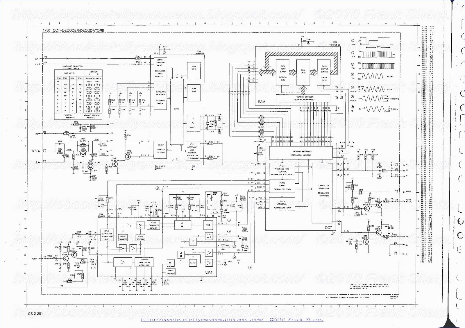


No comments:
Post a Comment
The most important thing to remember about the Comment Rules is this:
The determination of whether any comment is in compliance is at the sole discretion of this blog’s owner.
Comments on this blog may be blocked or deleted at any time.
Fair people are getting fair reply. Spam and useless crap and filthy comments / scrapers / observations goes all directly to My Private HELL without even appearing in public !!!
The fact that a comment is permitted in no way constitutes an endorsement of any view expressed, fact alleged, or link provided in that comment by the administrator of this site.
This means that there may be a delay between the submission and the eventual appearance of your comment.
Requiring blog comments to obey well-defined rules does not infringe on the free speech of commenters.
Resisting the tide of post-modernity may be difficult, but I will attempt it anyway.
Your choice.........Live or DIE.
That indeed is where your liberty lies.
Note: Only a member of this blog may post a comment.