


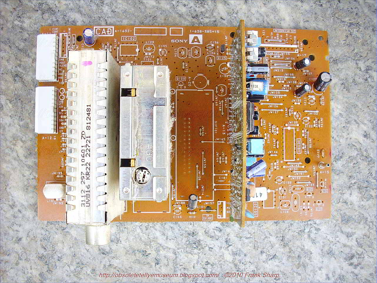


SONY KV-X2151A CHASSIS AE-1B 90° CIRCUITS DESCRIPTIONS:
-------------------------------
TDA4555 Multistandard decoder.
GENERAL DESCRIPTION
The TDA4555 and TDA4556 are monolithic integratedmultistandard colour decoders for the PAL, SECAM,
NTSC 3,58 MHz and NTSC 4,43 MHz standards. The
difference between the TDA4555 and TDA4556 is the
polarity of the colour difference output signals (B-Y)
and (R-Y).
Features
Chrominance part
· Gain controlled chrominance amplifier for PAL, SECAM
and NTSC
· ACC rectifier circuits (PAL/NTSC, SECAM)
· Burst blanking (PAL) in front of 64 ms glass delay line
· Chrominance output stage for driving the 64 ms glass
delay line (PAL, SECAM)
· Limiter stages for direct and delayed SECAM signal
· SECAM permutator
Demodulator part
· Flyback blanking incorporated in the two synchronous
demodulators (PAL, NTSC)
· PAL switch
· Internal PAL matrix
· Two quadrature demodulators with external reference
tuned circuits (SECAM)
· Internal filtering of residual carrier
· De-emphasis (SECAM)
· Insertion of reference voltages as achromatic value
(SECAM) in the (B-Y) and (R-Y) colour difference output
stages (blanking)
Identification part
· Automatic standard recognition by sequential inquiry
· Delay for colour-on and scanning-on
· Reliable SECAM identification by PAL priority circuit
· Forced switch-on of a standard
· Four switching voltages for chrominance filters, traps
and crystals
· Two identification circuits for PAL/SECAM (H/2) and
NTSC
· PAL/SECAM flip-flop
· SECAM identification mode switch (horizontal, vertical
or combined horizontal and vertical)
· Crystal oscillator with divider stages and PLL circuitry
(PAL, NTSC) for double colour subcarrier frequency
· HUE control (NTSC)
· Service switch.
SIEMENS TV Stereo Decoder with Matrix TDA6600-2
Preliminary Data Bipolar IC:The TDA6600-2 includes an advanced decoder for the identification signals for the
multichannel TV sound systems according to the dual-carrier system as well as a matrix
switched by the decoder to provide the L-Ft-information.
Features
0 Increased switching reliability and recognition by means of two PLLs for stereo
(117 Hz) and / or dual channel (274 Hz)
0 Separate bandwidth selection for dual-tone (pins 17-18) and stereo (pins 14-15)
0 Separate setting for the PLL time constants for dual-tone (pin 10) and stereo (pin 11)
0 Adjustable cut level for dual-tone (pin 8) and stereo (pin 9)
0 Cross-talk rejection independent of external component accuracy
0 Adjustment to minimal cross-talk level through external DC voltage
0 Suitable for TV sets with a 15625-Hz signal.
Type Ordering Code Package
TDA 6600-2 Q67000-A8210 P-DlP-24
Circuit Description
The circuitry has two functional sections:
Two phase locked loops for generating the required comparison frequencies (54.96
kHz and 54.8 kHz) from the line frequency. The phase detectors of the control loops
operate in a frequency range of 117 Hz and/or 274 Hz.
Four demodulators to evaluate the 54-kHz pilot signal. The capacitors at the mixer
outputs determine the bandwidth (and thus the signal-to-noise ratio) of the pilot tone
recognition.
An evaluation circuitry for decoding "stereo", "dual sound", and "mono" from the mixer
output levels. ln order to assure interference-free operation in case of high noise level
input signals, the individual signals "stereo" and "dual sound" are delayed via an
externally adjustable integrator. The subsequent digital evaluation provides the
information "mono", "dual sound", or "stereo" to the matrix and the 4 level input/output
(to drive the TDA 6200). If this four level input/output is connected to ground externally
(e.g. by the TDA 6200), the decoder will recognize this signal as "forced mono".
A stereo matrix with deemphasis and SCART output switched by the pilot frequency
decoder. The SCART output can be disabled by a MUTE signal (coincidence).
SONY KV-X2151A CHASSIS AE-1C 90° TEA2028 COLOR TV SCANNING AND POWER SUPPLY PROCESSOR
the TEA2028 combines 3
major functionsof a TV set as follows :
- Horizontal (line) and vertical (frame) time basegeneration for spot deviation. The video signal is
used for the synchronization of both time bases.
- On-chip switching power supply controller synchronized
on line frequency.
This integrated circuit has been implemented in
bipolar I2L technology, and various functions are
digitally processed. In fact, resorting to logic functions
has the advantage of working with pure and
accurate signals while full benefit is drawn from
high integration of logic gates (approx. 110 gates
per mm2).
The main objective is to drive all functions using an
accurate time base generated by a master 500kHz
oscillator.
Also, horizontal and vertical time bases, are obtained
by binary division of reference frequency.
This has the advantage of eliminating the 2 adjustments
which were necessary in former devices.
One section of this integrated circuit is designed to
drive a switching power supply of recent implementation
called ”master-slave”. Switching takes place
on the primary side (i.e., directly on mains) of a
transformer. The device ensures SMPS Control,
Start-up and Protection functions.Control signals
go through a small pulse transformer thereby providing
full isolation from mains supply.
This new approach fully eliminates the bulky mains
transformersused in the past. In addition, it offers
optimized power consumption and reduction of TV
cost-price.
- MAIN FUNCTIONS
- Detection and extraction of line and frame synchronization
pulses from the composite video
signal.
- Horizontal scanning control and synchronization
by two phase-locked loop devices.
- Video identification.
- 50 or 60Hz standardrecognition for vertical scanning.
- Generation of a self-synchronized frame sawtooth
for 50/60Hz standards.
- Line time constant switching for VCR operation
through an input labeled ”VCR” (Video Cassette
Recorder).
- Control and regulation of a primary-connected
switching power supply by on-chip controller device
combining :
• an error amplifier
• a pulse width modulator synchronized on line
frequency
• a start-up and protection system
- Overall TV set protection input
- Frame blanking and super sandcastle output signals
- Frame blanking safety input for CRT protection in
case of vertical stage failure.
Internal Voltage and Current References
V.1.1 - 1.26V Voltage reference
For optimum operation of the device, an accurate
and temperature-stable voltage generator independent
from VCC variations is used (Band-gap
type generator).
The generated 1.26V is particularly used as reference
setting on input comparators.
Line Sync. Extraction
Horizontal and vertical time bases should be synchronized
with corresponding sync. pulses transmitted
inside the infra-black portion of video signal.
The duty of this stage is to extract these sync
pulses. The output signal, called composite sync,
contains the vertical sync which is transmitted by
simple inversion of line sync. pulses.
The vertical sync pulse is then extracted from this
composite signal.
The main advantage of this arrangement is its
ability to operate at video input signal levels falling
within 0.2V to 3V peak-to-peak range and at any
average value.
The operating principle is to lock the black level of
the input signal (Pin 27) onto internaly fixed voltage
(VN) and then memorize the average voltage of the
sync pulse by using an integrating capacitor connected
to Pin 26.
Finally, the composite sync signal is delivered by a
comparator the inputs of which are driven by V50%
and video signals.
The video signal is applied to Pin 27 through the
coupling capacitor ”C27”. Since the sync pulse
amplitudeisgenerallyequal to 1/3 ofVPP (i.e.66mV
to 1V) and in order to obtaina good precision of the
black level, the sync pulse should be amplified by
a coefficient of - 14 before being applied to the
comparator ”C1”.
This comparator will charge the ”C27” capacitoras
long as VS1 >VN V VS1 will stabilize at VN during the
line flyback interval ”Tr” if the average charge of
”C27” capacitor is nil for one TH period.
IC/ID is calculated such that the locking occurs at
the middle of the back porch.
- Memorizing the sync pulse 50% value
The objective is to memorize the voltage corresponding
to 50% of theline sync pulseVS1 byusing
an external capacitor connected to Pin 26 (see
Figure 9).
The overall arrangement comprises two comparators.
- Comparator C2 : delivers an output voltage ”V1”
by comparingVS1 +VD, V26 and the voltage drop
across two resistors.
- ComparatorC3 : which delivers a constant output
current thereby maintaining on capacitor ”C26”,
the voltage V50% corresponding to 50% of peak
to peak sync pulse.
Sync pulse detection
This function is fulfilled by comparing the inverted
video signal (VS1 + VD) whose black level is constantat 2V, with the sync 50% voltage level on
Pin 26 (see Figure 10).
Comparator C4 will deliver the line sync pulse (LS)
which will be used for 3 functions :
- Horizontal scanning frequency locking : output to
j1 phase comparator.
- Frame sync extraction for vertical scanning synchronization.
- Detecting the presence of a video signal at circuit
input.
The LS signal in two latter functions is filtered for
noise by using combination of current generator I
and a zener diode equivalent to a capacitor.
Using this extraction technique at a very noisy
video signal yields remarkable display stability.
First Phase Locked-loop Stage ”j1”
This stage is commonly called the first Phase
Locked-Loop ”j1”.
Its duty is to lock the frequency and the phase of
the horizontal time base with respect to the line
sync signal.
In the absence of transmission (i.e. lack of line
sync), the horizontal scanning frequency is obtained
by dividing the output frequency of a VCO
device. This VCO oscillates at approximately
500kHz and uses a low frequency drift ceramic
resonator.This method eliminates the need of horizontal
frequency adjustment.
VCO centered on 500kHz
This is a voltage-controlled oscillator which generates
an output frequency proportional to the voltage
applied to its input.
This voltage is delivered by low-pass filter.
VCO (Voltage Controlled Oscillator)
Its function is to generatea frequency proportional
to a control voltage issued externally, by the lowpass
filter in our case.
The period of the output signal is used as timing
reference for various functions such as, horizontal
and vertical time bases. The frequency range must
be short and accurate :
- It must be short since the power dissipated within
the horizontal scanning block is inversely proportional
to the line frequency.
- The accuracy is required if the adjustment is to
be omitted.
The basic arrangement is to employ a ceramic
resonator (or ceramic filter) which has quite stable
characteristics as a function of frequency.
A filter whose resonating frequency is a multiple of
line frequency (15625Hz) is to be selected. An
example is 32 V 15625 = 500kHz.
Video identification stage
This stage will detect the coincidence between the
line sync pulse (if present) and a 2ms pulse issued
from the logic block. This 2ms pulse at line frequency
is positionned at the center of line sync
pulse when the first loop ”j1” is locked.
This sampled detection is stored by an external
capacitor connected to Pin 25. The video recognition
status is also available on Pin 24 so as to
enable Sound Muting during station search process
and the inhibition of Automatic FrequencyTuning.
- Generates the saw-tooth current for line yoke
- Generates the high voltage required by picture
tube and other supply voltages
The line flyback information is provided by the
EHT transformer.
Line deflection stage
This chapter will cover a general description of the
”horizontal deflection stage” employed almost
commonly in all recent TV sets.
Deflection of electron beam is proportional to the
intensity of magnetic field induced by the line yoke.
This yoke is equivalent to an inductor. The deflection
is therefore proportional to the current through
inductor.
In order to obtain a linear deflection from left to right
as a function of time, a saw-tooth current must be
generated within the yoke.The approachis toapply
a switched DC voltage to the line yoke.
Vertical deflection driver stage
This stage must constantly drive the vertical spot
deflection.Such deflectionwill horizontallyscan the
screen from top to bottom thus generating the
displayed image. Similar to horizontal deflection,
the vertical deflection is obtained by magnetic field
variations of a coil mounted on the picture tube.
A saw-tooth current at frame frequency will go
through this coil commonly called ”frame yoke”.
Frame period is the time required for the entire
screen to be scanned vertically.
C.C.I.R.and N.T.S.C.TVstandardsrequirerespectively
50Hz and 60Hz Frame Scanning Frequencies.
Also, a full screen display is obtained by two
successivevertical scanningssuch that the second
scanning is delayed by a half line period with
respect to the first.
This method increases the number of images per
second (50 half images/s or 50 frames/s in 50Hz
standard). This scanning mode called ”Interlaced
Scanning” eliminates the fliker which would have
been otherwise produced by scanning 25 entire
images per second.
The circuit will generate a saw-tooth voltage whichis linear as a function of time and called ”frame
saw-tooth”. A power amplifier will deliver to the
”frame yoke” a current proportional to this sawtooth
voltage. It is thus clear that this saw-tooth
voltage reflects the function of the vertical spot
deflection; which must itself be synchronized with
the video signal. Synchronization signals are obtained
from an extraction stage which will extract
the useful signal during line pulse inversion of the
composite sync signal.
Synchronization occurs at the end of scanning, in
other words, when the saw-tooth voltage at Pin 5
is reset. This function is accomplished by the
”frame logic circuitry” of full digital implementation.
This processing method offers various advantages
:
- Accurate free-running scanning frequency
eliminates the frequencyadjustment required by
previous devices.
- Digital synchronization locked onto half line
frequency thereby yielding perfect interlaced display
andexcellent stabilitywith noisy videosignal.
- Automatic 50/60Hz standard recognition and
switching the corresponding display amplitude.
- Optimized synchronization in VCR mode.
- Generationof variousaccurate time intervals,
such as narrow ”sync windows” thus reducing
considerably the vertical image instability in case
of for instance,mainsinterference,superimposed
on frame sync pulse.
- Generation of vertical blanking signal for spot
flyback and to protect the picture tube in case
of scanning failure.
Vertical synchronization window -
Free-running period
In the absence of sync pulse various free-running
periods are specified. Since vertical scanningmust
be always active, these free-running periods must
be higher than those of 50 and 60Hz standards so
as to ensure synchronization.
An other window, allowing synchronization only at
the end of scanning, is also necessary. Upon synchronization,
this window will allow vertical flybackonly at the bottom of screen. This window should
be narrow for good noise immunity but also wide
enough to yield, upon synchronization, a capture
time unperceptible on screen.
In our case, as long as no standard identification
takes place the window will remain wide, and once
one of the standards has been identified, the window
will be considerably reduced.
InVCRmode, thiswindow will bealways wide since
frame frequenciesdelivered in high-speed search,
slow review and picture pause modes are very
much variable and must be taken into consideration.
In the absenceof transmission (Mute = 0), synchronization
is disabled (so as to avoid incorrect synchronization
due to noise) and the free-running
frequency is around 50Hz. This will eliminate the
occurrence of picture overlay at the end of trace at
a lower free-running frequency.
- Frame blanking safety (TEA2028 only,for TEA2029 refer to section VII.5)
Its duty is to protect the phosphorcoating of picture
tube in case of any problem with vertical deflection
function such as scanning failure.
Asignal to monitor correct scanning is provided by
the frame yoke and applied to Pin 2.
In case of any failure, all frame blanking outputsare
disabled and go high thereby blanking the entire
screen.
During trace phase, the voltage across frame yoke
has a parabolicalshape due to the couplingcapacitor
in series with yoke. During frame flyback, the
current through frame yoke must be rapidly inverted.
Conventionally, a two-fold higher supply
voltage is applied across the yoke. This will produce
an overvoltage called ”flyback”.
The safety monitoring status is detected on the
falling-edge of flyback, i.e. at the beginning of
scanning. A differentiator network is used to transmit
only fast voltage variations.
Therequiredpulse is then compared to 1.26Vlevel.
Frame blanking goes high in the absence of negative
pulse (zero deflection current) or if the pulse
does not fall within the first 21 lines (exagerated
over-scanning).
SWITCHING POWER SUPPLY DRIVER STAGE
Switching takes place on the primary side (mains
side) of a transformer by using TEA2164 SMPS
Controller manufactured by SGS-THOMSON.Required voltage values are obtained by rectifying
different voltage outputs delivered through secondary
windings. The horizontal deflection stage is
powered by one of these outputs delivering around
hundred volts.
This voltage source must be regulated since any
voltage fluctuation will yield variations of the horizontal
display amplitude.
The TE2028 monitors this voltage and transmits
the regulation signal to the primary controller circuitry
via a small pulse transformer. The characteristics
of this regulation signal are directly related
to the conduction period of switching transistor.
General operating principles
A fraction of the 135V output voltage to be regulated
is compared to the 1.26V reference voltage.
Resulting error signal is amplified and then applied
to phase modulator ”M1”, which will deliver a
square waveform at line frequency whose duty
cycle depends on the value of input voltage ”V9”.
A second phase modulator ”M2” will determine the
conduction period as a function of voltage on
Pin 15. This function is mandatory for system startup.
A 28ms window is used to limit the conduction
period of the primary-connected transistor.
Supply output (Pin 7) and line output (Pin 10) will
be disabled if any information indicating abnormal
operation is applied to safety input (Pin 28). Consequently,
all power stages are disabled and the
TV set is thus protected.
SMPS WAVEFORMS
For discontinous mode ”flyback” configuration
The primary-connected transistor is turned-off during
the line flyback.
All interference signals due to switching and susceptible
to affect the video signal will not therefore
be visible on screen.
Power supply soft-start
When theTVset is initially turned on,control pulses
are not yet available and consequently the controller
block on primary side will impose a low-power
transfer to the secondary winding. This power is
produced by an intermittent switching mode called
”Burst Mode”.
 As soon as the VCC supply to TEA2028Bexceeds
6V level, line andSMPSoutputsareenabled.Since
the filtering capactitors on secondary side cannot
charge up instantaneously,the voltage to be regulated
would not yet be at its nominal value.Without
conduction period limitation upon start-up, the device
will set a maximum cycle of 28ms which will
result in a high current flow through the primary
winding and thus through the switching transistor
which will in turn activate the protection function
implemented on primary side.
Consequently, the primary controller block will be
inhibited and the set will not turn-on.
A start-up system has been implemented within
TEA2028B to overcome this problem.
This soft start system, will upon initial start-up, use
the image of the falling voltage on Pin 15 to increase
progressively the conduction cycle. The
phase modulator ”M2” compares this voltage with
line saw-tooth voltage and delivers the corresponding
limitation cycle.
During supply voltage rising cycle [VCC (Pin 8)
< 6V], the capacitor Pin 15 will charge up rapidly
while the voltage across it follows VCC.
At VCC . 6V, the capacitor is discharged via an
internal current generatorand the voltage across it
decays linearly.
At V15 3 3.5V (line saw-tooth peak-to-peak voltage),
phase comparator ”M2” delivers a low conductionperiod which will gradually increase.
The conduction period (Pin 7) will rise until the
secondary voltage reaches the value set by potentiometer
”P”. When this occurs, the loop is activated.
The Pin 15 discharge current value is 100mA for a
duration of 2ms line frequency.
- Protection features
As soon asa safety signal (V 3 1.26V) is applied to
Pin 28, line and supply outputs (Pins 10 and 7) are
both disabled. Capacitor ”C15” begins charging up
until the voltage across it reaches 4V (K V VCC).
Outputs are again enabled and conduction period
gradually increases as it occurs upon initial startup.
The device will be definitively inhibited if the cycle
of events is repeated 3 times.
For the device to restart, the internal 3-bit register
should be reset which requiresthe VCC to fall below
4V (see Figure 68).
Pin 15 charging current : IC(AV) = - ID(AV) = - 3.1mA
TV Power supply in standby mode
V.7.6.1 - Regulationby primary controller circuit
This mode of regulation called ”Burst Mode” is
performedonly by the primary controller circuit and
is activated in the case of missing control pulses or
in the absence of power supply to TEA2028B.
In this mode, power available through secondary
winding is limited. Refer to TEA2164 ApplicationNote for further details.
Higher powers can be obtained by using the regulation
feature offered by TEA2028B. In this case,
the horizontal output (Pin 10) must be disabled.
V.7.6.2 - Regulation by TEA2028
In this case, all that is required is to disable the line
scanning function thus reducing the overall power
by 90%.
The device power supply regulation loop remains
active, for minimum conduction period to be 1.5ms
the power delivered through secondary must be
higher than 3W.
Line Output Inhibition
Two alternativesare possible :
- Grounding flip-flop Pin 1
- Apply a voltage higher than 3V to Pin 12.
Super sandcastle signal generator
This signal used in video stage, is available on
Pin 11.
It has 3 levels at specified time intervals :
- 2.5V level
Used for vertical blanking at each frame flyback.
Its duration is 21 lines and is generated by the
frame logic.
This level will be maintained if vertical scanning
failure is detected on Pin 2.
- 4.5V level
Used for horizontal blanking, its duration is determined
by comparing the line flyback signal on
Pin 12 to an internal voltage of 0.25V.
- 10V level
This signal is used by color decoding stage. Its
duration of 4ms is determined by line logic circuitry.
With respect to the video signal on Pin 27,
this level is positioned such that it is used to
sample the burst frequency transmitted just after
the sync pulse.
TDA4565
Colour transient improvement
circuit
GENERAL DESCRIPTIONThe TDA4565 is a monolithic integrated circuit for colour transient improvement (CTI) and luminance delay line in gyrator
technique in colour television receivers.
Features
· Colour transient improvement for colour difference signals (R-Y) and (B-Y) with transient detecting-, storage- and
switching stages resulting in high transients of colour difference output signals
· A luminance signal path (Y) which substitutes the conventional Y-delay coil with an integrated Y-delay line
· Switchable delay time from 730 ns to 1000 ns in steps of 90 ns and additional fine adjustment of 50 ns
· Two Y output signals; one of 180 ns less delay.
TDA2556 QUASI-SPLIT-SOUND CIRCUIT WITH DUAL SOUND DEMODULATORS
GENERAL DESCRIPTION
The TDA2556 is a monolithic integrated circuit for quasi-split-sound processing, including two FM
demodulators, for two carrier stereo TV receivers and VTR.
Features
First IF (vision carrier plus sound carrier).
0 3 stage gain controlled IF amplifier
0 AGC circuit
0 Reference amplifier and limiter amplifier for vision carrier (V.C.) processing
0 Linear multiplier for quadrature demodulation
Second IF (two separate channels for both FM sound signals).
0 4-stage-limiting amplifier
0 Ouadrature demodulator
0 AF amplifier with de-emphasis
O Output buffer
0 Muting for one or both AF outputs
SONY KV-X2151A CHASSIS AE-1C 90° TEA2164 /2165 SWITCH MODE POWER SUPPLY PRIMARY CIRCUIT
.POSITIVE AND NEGATIVE OUTPUT CURRENTUP TO 1.2AAND – 1.7A .A TWO LEVEL COLLECTOR CURRENT LIMITATION
.COMPLETE TURN OFF AFTER LONG DURATION
OVERLOADS .UNDER AND OVER VOLTAGELOCK-OUT .SOFT START BY PROGRESSIVE CURRENT
LIMITATION .DOUBLE PULSE SUPPRESSION .BURST MODE OPERATION UNDER STANDBY
CONDITIONS
DESCRIPTION

In amaster slave architecture, the TEA2164control
IC achieves the slave function. Primarily designed
for TV receivers and monitors applications, this
circuit provides an easy synchronizationand smart
solution for low power stand by operation.
Located at the primary side the TEA2164 Control
IC ensures :
- the power supply start-up
- the power supply control under stand-by conditions
- the process of the regulation signals sent by the
master circuit located at the secondary side
- directbasedrive of the bipolarswitching transistor
- the protection of the transistor and the power
supply under abnormal conditions.
II. GENERAL DESCRIPTION
In a master slave architecture, the TEA2164 Control
IC, located at the primary side of an off line
power supply achievesthe slave function ;whereas
the master circuit is located at the secondary side.
The link between both circuits is realized by a small
pulse transformer

In the operation of the master-slave architecture,
four majors cases must be considered :
- normal operating
- stand-bymode
- power supply start-up
- abnormal conditions : off load, short circuit, ...
II.1. Normal Operating (master slave mode)
In this configuration, the master circuit generatesa
pulse widthmodulatedsignal issued from themonitoring
of the output voltage which needs the best
accuracy (in TV applications : the horizontal deflection
stagesupplyvoltage).Themaster circuit power
supply can be supplied by another output.
The PWM signal are sent towards the primary side
through small differentiating transformer. For the
TEA2164 positive pulses are transistor switchingon
commands ; and negative pulses are transistor
switching-offcommands (Figure 4). In this configuration,
only by synchronizing the master oscillator,
the switching transistor may be synchronized with
an external signal.
II.2. Stand-by Mode
In this configuration the master circuit no longer
sends PWM signals, the structure is not synchronized
; and the TEA2164 operates in burst mode.
The average power consumption at the secondary
side may be very low 1W 3 P 3 6W (as it is
consumed in TV set during stand by).
By action on the maximum duty cycle control, a
primary loop maintains a semi-regulation of the
output voltages.Voltage on feed-back is applied on
Pin 9.
Burst period is externally programmedby capacitor
C1.
II.3. Power Supply Start-up
After the mains have been switched-on, the VCCstorage capacitor of the TEA2164 is charged
through a high value resistor connected to the
rectified high voltage.When Vcc reaches VCC start
threshold (9V typ), the TEA2164 starts operatingin
burst mode. Since available output power is low in
burst mode the output power consumption must
remain low before complete setting-up of output
voltage. In TV application it can be achieved by
maintaining the TV in stand-by mode during startup.
Overvoltage Protection
When VCC exceeds VCC max, an internal flip-flop
stops output conduction signals. The circuit will
start again after the capacitor C1 discharge ; it
means : after loss of synchronization or after Vcc
stop crossing (Figure 7).
In flyback converters, this function protects the
power supply against output voltage runaway.
SONY KV-X2151A CHASSIS AE-1C 90° Synchronized switch-mode power supply:
In a switch mode power supply, a first switching transistor is coupled to a primary winding of an isolation transformer. A second switching transistor periodically applies a low impedance across a second winding of the transformer that is coupled to an oscillator for synchronizing the oscillator to the horizontal frequency. A third winding of the transformer is coupled via a switching diode to a capacitor of a control circuit for developing a DC control voltage in the capacitor that v
aries in accordance with a supply voltage B+. The control voltage is applied via the transformer to a pulse width modulator that is responsive to the oscillator output signal for producing a pulse-width modulated control signal. The control signal is applied to a mains coupled chopper transistor for generating and regulating the supply voltage B+ in accordance with the pulse width modulation of the control signal.Description:
The invention relates to switch-mode power supplies.
Some television receivers have signal terminals for receiving, for example, external video input signals such as R, G and B input signals, that are to be developed relative to the common conductor of the receiver. Such signal terminals and the receiver common conductor may be coupled to corresponding signal terminals and common conductors of external devices, such as, for example, a VCR or a teletext decoder.
To simplify the coupling of signals between the external devices and the television receiver, the common conductors of the receiver and of the external devices are connected together so that all are at the same potential. The signal lines of each external device are coupled to the corresponding signal terminals of the receiver. In such an arrangement, the common conductor of each device, such as of the television receiver, may be held "floating", or conductively isolated, relative to the corresponding AC mains supply source that energizes the device. When the common conductor is held floating, a user touching a terminal that is at the potential of the common conductor will not suffer an electrical shock.
Therefore, it may be desirable to isolate the common conductor, or ground, of, for example, the television receiver from the potentials of the terminals of the AC mains supply source that provide power to the television receiver. Such isolation is typically achieved by a transformer. The isolated common conductor is sometimes referred to as a "cold" ground conductor.
In a typical switch mode power supply (SMPS) of a television receiver the AC mains supply voltage is coupled, for example, directly, and without using transformer coupling, to a bridge rectifier. An unregulated direct current (DC) input supply vo
ltage is produced that is, for example, referenced to a common conductor, referred to as "hot" ground, and that is conductively isolated from the cold ground conductor. A pulse width modulator controls the duty cycle of a chopper transistor switch that applies the unregulated supply voltage across a primary winding of an isolating flyback transformer. A flyback voltage at a frequency that is determined by the modulator is developed at a secondary winding of the transformer and is rectified to produce a DC output supply voltage such as a voltage B+ that energizes a horizontal deflection circuit of the television receiver. The primary winding of the flyback transformer is, for example, conductively coupled to the hot ground conductor. The secondary winding of the flyback transformer and voltage B+ may be conductively isolated from the hot ground conductor by the hot-cold barrier formed by the transformer.It may be desirable to synchronize the operation of the chopper transistor to horizontal scanning frequency for preventing the occurrence of an objectionable visual pattern in an image displayed in a display of the television receiver.
It may be further desirable to couple a horizontal synchronizing signal that is referenced to the cold ground to the pulse-width modulator that is referenced to the hot ground such that isolation is maintained.
A synchronized switch mode power supply, embodying an aspect of the invention, includes a transfromer having first and second windings. A first switching arrangement is coupled to the first winding for generating a first switching current in the first winding to periodically energize the second winding. A source of a synchronizing input signal at a frequency that is related to a deflection frequency is provided. A second switching arrangement responsive to the input signal and coupled to the second winding periodically applies a low impedance across the energized second winding that by transformer action produces a substantial increase in the first switching current. A periodic first control signal is generated. The increase in the first switching current is sensed to synchronize the first control signal to the input signal. An output supply voltage is generated from an input supply voltage in accordance with the first control signal.SONY KV-X2151A CHASSIS AE-1C 90° Switch-mode power supply with burst mode standby operation:
In a switch mode power supply, a first switching transistor is coupled to a primary winding of a transformer for generating pulses of a switching current. A secondar
y winding of the transformer is coupled via a switching diode to a capacitor of a control circuit for developing a control signal in the capacitor. The control signal is applied to a mains coupled chopper second transistor for generating and regulating supply voltages in accordance with pulse width modulation of the control signal. During standby operation, the first and second transistors operate in a burst mode that is repetitive at a frequency of the AC mains supply voltage such as 50 Hz. In the burst mode operation, during intervals in which pulses of the switching current occur, the pulse width and peak amplitude of the switching current pulses progressively increase in accordance with the waveform of the mains supply voltage to provide a soft start operation in the standby mode of operation within each burst group.Description:
The invention relates to switch-mode power supplies.
In a typical switch mode power supply (SMPS) of a television receiver the AC mains supply voltage is coupled to a bridge rectifier. An unregulated direct current (DC) input supply voltage is produced. A pulse width modulator controls the duty cycle of a chopper transistor switch that applies the unregulated supply voltage across a primary winding of a flyback transformer. A flyback voltage at a frequency that is determined by the modulator is developed at a secondary winding of the transformer and is rectified to produce DC output supply voltages such as a voltage B+ that energizes a horizontal deflection circuit of the television receiver and a voltage that energizes a remote control unit.
During normal operation, the DC output supply voltages are regulated by the pulse width modulator in a negative feedback manner. During standby operation, the SMPS is required to generate the DC output supply voltage that energizes the remote control unit. However, most other stages of the television receiver are inoperative and do not draw supply currents. Consequently, the average value of the duty cycle of the chopper transistor may have to be substantially lower during standby than during normal operation.
Because of, for example, storage time limitation in the chopper transistor, it may not be possible to reduce the length of the conduction interval in a given cycle below a minimum level. Thus, in order to maintain the average value of the duty cycle low, it may be desirable to operate the chopper transistor in an intermittent or burst mode, during standby. During standby, a long dead time interval occurs between consecutively occurring burst mode operation intervals. Only during the burst mode operation interval switching operation occurs in the chopper transistor. The result is that each of the conduction intervals is of a sufficient length.
In accordance with an aspect of the invention, burst mode operation intervals are initiated and occur at a rate that is determined by a repetitive signal at the frequency of the AC mains supply voltage. For example, when the mains supply voltage is at 50 Hz, each burst mode operation interval, when switching cycles occur, may last 5 milliseconds and the dead time interval when no switching cycles occur, may last during the remainder portion or 15 milliseconds. Such arrangement that is triggered by a signal at the frequency of the mains supply voltage simplifies the design of the SMPS.The burst mode operation intervals that occur in standby operation are synchronized to the 50 Hz signal. During each such interval, pulses of current are produced in transformers and inductances of the SMPS. The pulses of current occur in clusters that are repetitive at 50 Hz. The pulses of current occur at a frequency that is equal to the switching frequency of the chopper transistor within each burst mode operation interval. Such qurrent pulses might produce an objectionable sound during power-off or standby operation. The objectionable sound might be produced due to possible parasitic mechanical vibrations as a result of the pulse currents in, for example, the inductances and transformers of the SMPS.
In accordance with another aspect of the invention, the change in the AC mains supply voltage during each period causes the length of the conduction interval in consecutively occurring switching cycle during the burst mode operation interval to increase progressively. Such operation that occurs during each burst mode operation interval may be referred to as soft start operation. The soft start operation causes, for example, gradual charging of capacitors in the SMPS. Consequently, the parasitic mechanical vibrations are substantially reduced. Also, the frequency of the switching cycles within each burst mode operation interval is maintained above the audible range for further reducing the level of such audible noise during standby operation.
A switch mode power supply, embodying an aspect of the invention, for generating an output supply voltage during both a standby-mode of operation and during a run-mode of operation includes a source of AC mains input supply voltage. A control signal at a given frequency is generated. A switching arrangement energized by the input supply voltage and responsive to the first control signal produces a switching current during both the standby-mode of operation and the run-mode operation. The output supply voltage is generated from the switching current. An arrangement coupled to the switching arrangement and responsive to a standby-mode/run-mode control signal and to a signal at a frequency that is determined by a frequency of the AC mains input supply voltag
e controls the switching arrangement in a burst mode manner during the standby-mode of operation. During a burst interval, a plurality of switching cycles are performed and during an alternating dead time interval no switching cycles are performed. The two intervals alternate at a frequency that is determined by the frequency of the AC mains input supply voltage.TDA8442 I2C-bus interface for colour decoders
GENERAL DESCRIPTION
The TDA8442 provides control of four analogue functionsand has one high-current and two switching outputs.
Control of the IC is performed via the two-line, bidirectional
I2C-bus.
Features
· Four analogue control outputs
· One high-current output port (npn open emitter)
· Two switching output ports (npn collector with internal
pull-up resistor)
· I2C-bus slave receiver
· Power-down reset.
SIEMENS TDA 6200 TV Stereo Tone Control IC with Quasi-Stereo Section,
Channel 1/2 Switch, SCART Input, and I2C Bus ControlFeatures
0 Treble, bass, balance, and volume control by means of an integrated digital-to-analog
converter
I Quasi~stereo circuit during mono operation
0 Stereo basewidth expansion during stereo operation
O Physiological volume control
I Channel 1/2 switch-over during dual audio transmission
0 SCART connection
0 Control of all functions via the IZC bus and the bidirectional 4 level line of the
TDA 6600-2 (stereo demodulator IC)
O LED driver
0 Volume control range 80 dB
0 Treble, bass control 1 ‘I2 dB
O Channel separation min. 60 dB, cross-talk rejection min. 60 dB
O Parasitic voltage spacing up to 78 dB
Type W W Ordering Code Package
TDA 6200 Q67000-A2461 P-DIP-28
The TDA 6200 is comprised of a SCART switch-over, channel 1/2 switch-over, quasi-
stereo circuit, stereo basewidth expansion, physiological volume control, a treble, bass,
and volume control of the injected AF signals as well as an LED driver. The IC is
controlled by means of an FC bus serial interface as well as by the bidirectional 4 level
line from the TDA 6600-2. The component is used for AF sound signal processing in
stereo TV sets.
SONY KV-X2151A CHASSIS AE-1C 90° SONY DST EHT FBT TRANSFORMER Bobbin structure for high voltage transformers EHT Output.
A coil bobbin for a fly-back transformer or the like having a bobbin proper. A plurality of partition members or flanges are formed on the bobbin proper with a slot between adjacent ones. At least first and second coil units are formed in the bobbin proper, each having s everal slots, formed between the flanges, and first and second high voltage coils are wound on the first and second coil units in opposite directions, respectively. A rectifying means is connected in series to the first and second coil units, and a cut-off portion or recess is provided on each of the partition members. In this case, a wire lead of the coil units passes from one slot to an adjacent slot through the cut-off portion which is formed as a delta groove, and one side of the delta groove is corresponded to the tangent direction to the winding direction.
1. A fly-back transformer comprising a coil bobbin comprising a plurality of parallel spaced discs with a first adjacent plurality of said disc formed with delta shaped slots having first edges which extend tangentially to a first winding direction and a first winding wound on said first adjacent plurality of said discs in said first winding direction, a second adjacent plurality of said discs formed with delta shaped slots having first edges which extend tangentially to a second winding direction opposite said first winding direction and a second winding wound on said second adjacent plurality of said discs in said second winding direction, a third adjacent plurality of said discs formed with delta shaped slots having first edges which extend tangentially to said first winding direction and a third winding wound on said third adjacent plurality of said discs in said first winding direction and said second plurality of adjacent discs mounted between said first and third plurality of adjacent discs. 2. A fly-back transformer according to claim 1 wherein adjacent ones of said first adjacent plurality of discs are mounted such that their delta shaped slots are orientated 180 degrees relative to each other. 3. A fly-back transformer according to claim 2 including a first winding turning partition mounted between said first and second adjacent plurality of discs and formed with grooves and notches for changing winding direction between said first and second windings and a second winding turning partition mounted between said second and third adjacent plurality of discs and formed with grooves and notches for changing the winding direction between said second and third windings. 4. A fly-back transformer according to claim 3 wherein said first and second winding turning partitions are formed with winding guiding slots for guiding the winding between the first, second and third adjacent plurality of discs. 5. A fly-back transformer according to claim 2 including a first rectifying means connected between one end of said first winding and one end of said second winding, and a second rectifying means connected between the second end of said second winding and one end of said third winding. 6. A fly-back trans
former according to claim 5 wherein the second end of said first winding is grounded and a third rectifying means connected between the second end of said third winding and an output terminal.
Model: AE1, AE1A, AE1B, KV-211XML, KV-211XMTL, ...
A coil bobbin for a fly-back transformer or the like having a bobbin proper. A plurality of partition members or flanges are formed on the bobbin proper with a slot between adjacent ones. At least first and second coil units are formed in the bobbin proper, each having s
everal slots, formed between the flanges, and first and second high voltage coils are wound on the first and second coil units in opposite directions, respectively. A rectifying means is connected in series to the first and second coil units, and a cut-off portion or recess is provided on each of the partition members. In this case, a wire lead of the coil units passes from one slot to an adjacent slot through the cut-off portion which is formed as a delta groove, and one side of the delta groove is corresponded to the tangent direction to the winding direction. 1. A fly-back transformer comprising a coil bobbin comprising a plurality of parallel spaced discs with a first adjacent plurality of said disc formed with delta shaped slots having first edges which extend tangentially to a first winding direction and a first winding wound on said first adjacent plurality of said discs in said first winding direction, a second adjacent plurality of said discs formed with delta shaped slots having first edges which extend tangentially to a second winding direction opposite said first winding direction and a second winding wound on said second adjacent plurality of said discs in said second winding direction, a third adjacent plurality of said discs formed with delta shaped slots having first edges which extend tangentially to said first winding direction and a third winding wound on said third adjacent plurality of said discs in said first winding direction and said second plurality of adjacent discs mounted between said first and third plurality of adjacent discs. 2. A fly-back transformer according to claim 1 wherein adjacent ones of said first adjacent plurality of discs are mounted such that their delta shaped slots are orientated 180 degrees relative to each other. 3. A fly-back transformer according to claim 2 including a first winding turning partition mounted between said first and second adjacent plurality of discs and formed with grooves and notches for changing winding direction between said first and second windings and a second winding turning partition mounted between said second and third adjacent plurality of discs and formed with grooves and notches for changing the winding direction between said second and third windings. 4. A fly-back transformer according to claim 3 wherein said first and second winding turning partitions are formed with winding guiding slots for guiding the winding between the first, second and third adjacent plurality of discs. 5. A fly-back transformer according to claim 2 including a first rectifying means connected between one end of said first winding and one end of said second winding, and a second rectifying means connected between the second end of said second winding and one end of said third winding. 6. A fly-back trans
Description:
BACKGROUND OF THE INVENTION
1. Field of the Invention
The present invention relates generally to a bobbin structure for high voltage transformers, and is directed more particularly to a bobbin structure for high voltage transformer suitable for automatically winding coils thereon.
2. Description of the Prior Art
In the art, when a wire lead is reversely wound on a bobbin separately at every winding block, a boss is provided at every winding block and the wire lead is wound on one block, then one end of the wire lead is tied to the boss where it will be cut off. The end of the wire lead is tied to another boss, and then the wire lead is wound in the opposite direction. Therefore, the prior art winding method requires complicated procedures and the winding of the wire lead cannot be rapidly done and also the winding can not be performed automatically. Further, the goods made by the prior art method are rather unsatisfactory and have a low yield.
OBJECTS AND SUMMARY OF THE INVENTION
Accordingly an object of the invention is to provide a coil bobbin for a fly-back transformer or the like by which a wire lead can be automatically wound on winding blocks of the coil bobbin even though the winding direction is different among the different winding blocks.
Another object of the invention is to provide a coil bobbin for a fly-back transformer or the like in which a bridge member and an inverse engaging device for transferring a wire lead from one wiring block to an adjacent wiring block of the coil bobbin and wiring the wire lead in opposite wiring directions between adjacent wiring blocks, and a guide member for positively guiding the wire lead are provided.
According to an aspect of the present invention, a coil bobbin for a fly-back transformer or the like is provided which comprises a plurality of partition members forming a plurality of slots, a first coil unit having several slots on which a first high voltage coil is wound in one winding direction, a second coil unit having several slots on which a second high voltage coil is wound in the other direction, a rectifying means connected in series to the first and second coil units, and a cut-off portion provided on each of the partition members, a wire lead passing from one slot to an adjacent slot through the cut-off portions, each of the cut-off portions being formed as a delta groove, and one side of the delta groove corresponding to a tangent to the winding direction.
The other objects, features and advantages of the present invention will become apparent from the following description taken in conjunction with the accompanying drawings through which the like reference numerals and letters designate the same elements and parts, respectively.
BRIEF DESCRIPTION OF THE DRAWINGS
FIG. 1 is a schematic diagram showing the construction of a fly-back transformer;
FIG. 2 is a connection diagram showing an example of the electrical connection of the fly-back transformer shown in FIG. 1;
FIG. 3 is a schematic diagram showing an example of a device for automatically winding a wire lead of the fly-back transformer on its bobbin;
FIG. 4 is a perspective view showing an example of the coil bobbin according to the present invention;
FIG. 5 is a plan view of FIG. 4;
FIGS. 6 and 7 are views used for explaining recesses or cut-off portions shown in FIGS. 4 and 5; and FIGS. 8A and 8B cross-sectional views showing an example of the inverse engaging means according to the present invention.
DESCRIPTION OF THE PREFERRED EMBODIMENT
When the high voltage winding of a fly-back transformer used in a high voltage generating circuit of a television receiver is divided into plural ones and then wound on a bobbin, the divided windings (divided coils) are connected in serie s through a plurality of rectifying diodes.
When the winding is divided into, for example, three portions, such as divided coils La, Lb and Lc, they are wound on a bobbin proper 1 from, for example, left to right sequentially in this order as shown in FIG. 1. In this case, if the divided coils La and Lc are selected to have the same sense of turn and the middle coil Lb is selected to have the opposite sense of turn from the coils La and Lc, the distance between the terminal end of coil La and the start of coil Lb and the distance between the terminal end of coil Lb and the start of coil Lc can be got relatively long. Therefore, diodes Da and Db can be mounted by utilizing the space above the block on which the middle coil Lb is wound as shown in FIG. 1, so that it becomes useless to provide spaces for diodes between the divided coils La and Lb and between the divided coils Lb and Lc and hence the bobbin proper 1 can be made compact.
FIG. 2 is a connection diagram showing the connection of the above fly-back transformer. In FIG. 2, reference numeral 2 designates a primary winding (Primary coil) of the fly-back transformer, reference letter L designates its high voltage winding (secondary coil), including divided coils La, Lb and Lc, 3 an output terminal, and 4 a lead wire connected to the anode terminal of a cathode ray tube (not shown), respectively.
An example of the bobbin structure according to the invention, which is suitable to automatically wind coils, which are different in sense of turn in each winding block as shown in FIG. 1, on the bobbin, will be hereinafter described with reference to the drawings.
FIG. 3 is a diagram showing an automatic winding apparatus of a wire lead on a coil bobbin. If it is assumed that the wire lead is wound in the order of w inding blocks A, B and C in FIG. 1 and the wire lead is wound on the block A with the bobbin proper 1 being rotated in the counter-clockwise direction as shown in FIG. 3, the relation between the bobbin proper 1 and the wire lead becomes as shown in FIG. 3. In this figure, reference numeral 6 designates a bobbin for feeding the wire lead.
Turning to FIG. 4, an example 10 of the bobbin structure or coil bobbin according to the present invention will be described now. In this example, the winding blocks A, B and C for the divided coils La, Lb and Lc are respectively divided into plural slots or sections by plural partition members or flanges 11, and a cut-off portion or recess 12 is formed on each of the flanges 11 through which the wire lead in one section is transferred to the following winding section.
As shown in FIG. 6, each recess 12 is so formed that its one side extends in the direction substantially coincident with the tangent to the circle of the bobbin proper 1 and its direction is selected in response to the sense of turn of the winding or wire lead. In this case, the direction of recess 12 means the direction of the opening of recess 12, and the direction of recess 12 is selected opposite to the sense of turn of the wi nding in the present invention.
Now, recesses 12A, which are formed in the winding block A, will be now described by way of example. The positions of recesses 12A formed on an even flange 11Ae and an odd flange 11A 0 are different, for example, about 180° as shown in FIGS. 6A and 6B. Since the bobbin proper 1 is rotated in the counter-clockwise direction in the winding block A and hence the sense of turn of the wire lead is in the clockwise direction, the recess 12A is formed on the even flange 11Ae at the position shown in FIG. 6A. That is, the direction of recess 12A is inclined with respect to the rotating direction of bobbin proper 1 as shown in FIG. 6A. In this case, one side 13a of recess 12A is coincident with the tangent to the circle of bobbin proper 1, while the other side 13b of recess 12A is selected to have an oblique angle with respect to the side 13a so that the recess 12A has a predetermined opening angle.
The opening angle of recess 12A is important but the angle between the side 13a of recess 12A and the tangent to the circle of bobbin proper 1 is also important in the invention. When the wire lead is bridged or transferred from one section to the following section through the recess 12A, the wire lead in one section advances to the following section in contact with the side 13a of recess 12A since the bobbin proper 1 is rotated. In the invention, if the side 13a of recess 12A is selected to be extended in the direction coincident with the tangent to the circle of bobbin proper 1, the wire lead can smoothly advance from one section to the next section without being bent.
In the invention, since the middle divided coil Lb is wound opposite to the divided coil La, a recess 12B provided on each of flanges 11B of the winding block B is formed to have an opening opposite to that of recess 12A formed in the winding block A as shown in FIGS. 6C and 6D.
As shown in FIG. 5, terminal attaching recesses 14 are provided between the winding blocks A and B to which diodes are attached respectively. In the illustrated example of FIG. 5, a flange 15AB is formed between the flanges 11A 0 and 11B 0 of winding blocks A and B, and the recesses 14 are formed between the flanges 11A 0 and 15AB and between 15AB and 11B 0 at predetermined positions. Then, terminal plates 16, shown in FIG. 4, are inserted into the recesses 14 and then fixed there to, respectively. The terminal plates 16 are not shown in FIG. 5. Between the winding blocks B and C and between the blocks A and B, similar terminal attaching recesses 14 are formed, and terminal plates 16 are also inserted thereinto and then fixed thereto.
As described above, since the divided coil Lb is wound opposite to the divided coils La and Lc, it is necessary that the winding direction of the wire lead be changed when the wire lead goes from the block A to block B and also from the block B to block C, respectively.
Turning to FIG. 7, an example of the winding or wire lead guide means according to the present invention will be now described. In FIG. 7, there are mainly shown a bridge member for the wire lead and an inve rse member or means for the wire lead which are provided between the winding blocks A and B. At first, a bridge means 20 and its guide means 21, which form the bridge member, will be described. The bridge means 20 is provided by forming a cut-out portion or recess in the middle flange 15AB located between the winding blocks A and B. In close relation to the bridge means or recess 20, the guide means 21 is provided on a bridge section X A at the side of block A. This guide means 21 is formed as a guide piece which connects an edge portion 20a of recess 20 at the winding direction side to the flange 11A 0 of block A in the oblique direction along the winding direction through the section X A .
Next, an inverse engaging means 22 will be now described with reference to FIGS. 7 and 8. If the flange 11B 0 of FIG. 7 is viewed from the right side, the inverse engaging means 22 can be shown in FIG. 8A. In this case, the tip end of one side 13a of recess 12B 1 is formed as a projection which is extended outwards somewhat beyond the outer diameter of flange 11B 0 . The inverse engaging means 22 may take any configuration but it is necessary that when the rotating direction of the bobbin proper 1 is changed to the clockwise direction, the wire lead can be engaged with the recess 12B 1 or projection of one side 13a and then suitably transferred to the next station.
Another guide means 23 is provided on a bridge section X B at the side of winding block B in close relation to the inverse engaging means 22. The guide means 23 is formed as a guide surface which is a projected surface from the bottom surface of section X B and extended obliquely in the winding direction. This guide means or guide surface 23 is inclinded low into the means 22 and has an edge 23a which is continuously formed between the middle flange 15AB and the flange 11B 0 .
In this case, it is possible that the guide means 21 and guide surface 23 are formed to be the same in construction. That is, both the guide means 21 and 23 can be made of either the guide piece, which crosses the winding section or guide surface projected upwards from the bottom surface of the winding section. It is sufficient if the guide means 21 and 23 are formed to smoothly transfer the wire lead from one section to the next section under the bobbin proper 1 being rotated.
Although not shown, in connection with the middle flange 15BC between the winding blocks B and C, there are provided similar bridge means 20, guide means 21, inverse engaging means 22 and another guide means 23, respectively. In this case, since the winding direction of the wire lead is reversed, the forming directions of the means are reverse but their construction is substantially the same as that of the former means. Therefore, their detailed description will be omitted.
 According to the bobbin structure of the invention with the construction set forth above, the wire lead, which is transferred from the block A to the section X A by the rotation of bobbin proper 1, is wound on the section X B from the section X A after being guided by the guide piece 21 to the recess 20 provided on the middle flange 15AB, and then transferred to the recess 22 provided on the flange 11B 0 guide surface 23, bridged once to the first section of winding block B through the recess 22 (refer to dotted lines b in FIG. 7). Then, if the rotating direction of the bobbin proper 1 is reversed, the wire lead is engaged with the bottom of recess 22 (refer to solid lines b in FIG. 7). Thus, if the above reverse rotation of bobbin proper 1 is maintained, the wire lead is wound on the block B in the direction reverse to that of block A. When the wire lead is transferred from the block B to block C, the same effect as that above is achieved. Therefore, according to the present invention, the wire lead can be automatically and continuously wound on the bobbin proper 1.
After the single wire lead is continuously wound on blocks A, B and C of bobbin proper 1 as set forth above, the wire lead is cut at the substantially center of each of its bridging portions. Then, the cut ends of the wire lead are connected through diodes Da, Db and Dc at the terminal plates 16, respectively by solder.
In the present invention, the projection piece, which has the diameter greater than that of the flange 11B, is provided in the bridge recess 12 to form the inverse engaging means 22 as described above, so that when the winding direction is changed, the wire lead engages with the inverse engaging means 22 without errors when reversing the winding direction of the wire lead.
If the diameter of the projection piece of means 22 is selected, for example, to be the same as that of the flange 11B, it will not be certain that the wire lead engages with the means 22 because it depends upon the extra length of the wire lead and hence errors in winding cannot be positively avoided.
Further, in this invention, the bridge means is provided on the flange positioned at the bridging portion of the bobbin which has a number of dividing blocks separated by flanges, and the inverse engaging means is provided and also the guide means is provided at the former winding section to cooperate with the inverse engaging means. Therefore, the wire lead can be positively fed to the bridge means, and the transfer of the wire lead to the following winding section can be carried out smoothly.
Further, in this invention sinc
e one side of the recess 12 is selected coincident with the tangent of the outer circle of the bobbin proper 1 and also with the winding direction, the wire lead can be smoothly bridged to the following section. Due to the fact that the direction of recess 12 is changed in response to the winding direction, even if there is a block on which the wire lead is wound in the opposite direction to that of the other block, the wire lead can be continuously and automatically wound through the respective blocks.
The above description is given for the case where the present invention is applied to the coil bobbin for the high voltage winding of a fly-back transformer, but it will be clear that the present invention can be applied to other coil bobbins which require divided windings thereon with the same effects.
It will be apparent that many modifications and variations could be effected by one skilled in the art without departing from the spirits or scope of the novel concepts of the present invention, so that the spirits or scope of the invention should be determined by the appended claims only.
1. Field of the Invention
The present invention relates generally to a bobbin structure for high voltage transformers, and is directed more particularly to a bobbin structure for high voltage transformer suitable for automatically winding coils thereon.
2. Description of the Prior Art
In the art, when a wire lead is reversely wound on a bobbin separately at every winding block, a boss is provided at every winding block and the wire lead is wound on one block, then one end of the wire lead is tied to the boss where it will be cut off. The end of the wire lead is tied to another boss, and then the wire lead is wound in the opposite direction. Therefore, the prior art winding method requires complicated procedures and the winding of the wire lead cannot be rapidly done and also the winding can not be performed automatically. Further, the goods made by the prior art method are rather unsatisfactory and have a low yield.
OBJECTS AND SUMMARY OF THE INVENTION
Accordingly an object of the invention is to provide a coil bobbin for a fly-back transformer or the like by which a wire lead can be automatically wound on winding blocks of the coil bobbin even though the winding direction is different among the different winding blocks.
Another object of the invention is to provide a coil bobbin for a fly-back transformer or the like in which a bridge member and an inverse engaging device for transferring a wire lead from one wiring block to an adjacent wiring block of the coil bobbin and wiring the wire lead in opposite wiring directions between adjacent wiring blocks, and a guide member for positively guiding the wire lead are provided.
According to an aspect of the present invention, a coil bobbin for a fly-back transformer or the like is provided which comprises a plurality of partition members forming a plurality of slots, a first coil unit having several slots on which a first high voltage coil is wound in one winding direction, a second coil unit having several slots on which a second high voltage coil is wound in the other direction, a rectifying means connected in series to the first and second coil units, and a cut-off portion provided on each of the partition members, a wire lead passing from one slot to an adjacent slot through the cut-off portions, each of the cut-off portions being formed as a delta groove, and one side of the delta groove corresponding to a tangent to the winding direction.
The other objects, features and advantages of the present invention will become apparent from the following description taken in conjunction with the accompanying drawings through which the like reference numerals and letters designate the same elements and parts, respectively.
BRIEF DESCRIPTION OF THE DRAWINGS
FIG. 1 is a schematic diagram showing the construction of a fly-back transformer;
FIG. 2 is a connection diagram showing an example of the electrical connection of the fly-back transformer shown in FIG. 1;
FIG. 3 is a schematic diagram showing an example of a device for automatically winding a wire lead of the fly-back transformer on its bobbin;
FIG. 4 is a perspective view showing an example of the coil bobbin according to the present invention;
FIG. 5 is a plan view of FIG. 4;
FIGS. 6 and 7 are views used for explaining recesses or cut-off portions shown in FIGS. 4 and 5; and FIGS. 8A and 8B cross-sectional views showing an example of the inverse engaging means according to the present invention.
DESCRIPTION OF THE PREFERRED EMBODIMENT
When the high voltage winding of a fly-back transformer used in a high voltage generating circuit of a television receiver is divided into plural ones and then wound on a bobbin, the divided windings (divided coils) are connected in serie
 s through a plurality of rectifying diodes.
 When the winding is divided into, for example, three portions, such as divided coils La, Lb and Lc, they are wound on a bobbin proper 1 from, for example, left to right sequentially in this order as shown in FIG. 1. In this case, if the divided coils La and Lc are selected to have the same sense of turn and the middle coil Lb is selected to have the opposite sense of turn from the coils La and Lc, the distance between the terminal end of coil La and the start of coil Lb and the distance between the terminal end of coil Lb and the start of coil Lc can be got relatively long. Therefore, diodes Da and Db can be mounted by utilizing the space above the block on which the middle coil Lb is wound as shown in FIG. 1, so that it becomes useless to provide spaces for diodes between the divided coils La and Lb and between the divided coils Lb and Lc and hence the bobbin proper 1 can be made compact.
FIG. 2 is a connection diagram showing the connection of the above fly-back transformer. In FIG. 2, reference numeral 2 designates a primary winding (Primary coil) of the fly-back transformer, reference letter L designates its high voltage winding (secondary coil), including divided coils La, Lb and Lc, 3 an output terminal, and 4 a lead wire connected to the anode terminal of a cathode ray tube (not shown), respectively.
An example of the bobbin structure according to the invention, which is suitable to automatically wind coils, which are different in sense of turn in each winding block as shown in FIG. 1, on the bobbin, will be hereinafter described with reference to the drawings.
FIG. 3 is a diagram showing an automatic winding apparatus of a wire lead on a coil bobbin. If it is assumed that the wire lead is wound in the order of w
 inding blocks A, B and C in FIG. 1 and the wire lead is wound on the block A with the bobbin proper 1 being rotated in the counter-clockwise direction as shown in FIG. 3, the relation between the bobbin proper 1 and the wire lead becomes as shown in FIG. 3. In this figure, reference numeral 6 designates a bobbin for feeding the wire lead.
 Turning to FIG. 4, an example 10 of the bobbin structure or coil bobbin according to the present invention will be described now. In this example, the winding blocks A, B and C for the divided coils La, Lb and Lc are respectively divided into plural slots or sections by plural partition members or flanges 11, and a cut-off portion or recess 12 is formed on each of the flanges 11 through which the wire lead in one section is transferred to the following winding section.
As shown in FIG. 6, each recess 12 is so formed that its one side extends in the direction substantially coincident with the tangent to the circle of the bobbin proper 1 and its direction is selected in response to the sense of turn of the winding or wire lead. In this case, the direction of recess 12 means the direction of the opening of recess 12, and the direction of recess 12 is selected opposite to the sense of turn of the wi
 nding in the present invention.
 Now, recesses 12A, which are formed in the winding block A, will be now described by way of example. The positions of recesses 12A formed on an even flange 11Ae and an odd flange 11A 0 are different, for example, about 180° as shown in FIGS. 6A and 6B. Since the bobbin proper 1 is rotated in the counter-clockwise direction in the winding block A and hence the sense of turn of the wire lead is in the clockwise direction, the recess 12A is formed on the even flange 11Ae at the position shown in FIG. 6A. That is, the direction of recess 12A is inclined with respect to the rotating direction of bobbin proper 1 as shown in FIG. 6A. In this case, one side 13a of recess 12A is coincident with the tangent to the circle of bobbin proper 1, while the other side 13b of recess 12A is selected to have an oblique angle with respect to the side 13a so that the recess 12A has a predetermined opening angle.
The opening angle of recess 12A is important but the angle between the side 13a of recess 12A and the tangent to the circle of bobbin proper 1 is also important in the invention. When the wire lead is bridged or transferred from one section to the following section through the recess 12A, the wire lead in one section advances to the following section in contact with the side 13a of recess 12A since the bobbin proper 1 is rotated. In the invention, if the side 13a of recess 12A is selected to be extended in the direction coincident with the tangent to the circle of bobbin proper 1, the wire lead can smoothly advance from one section to the next section without being bent.
In the invention, since the middle divided coil Lb is wound opposite to the divided coil La, a recess 12B provided on each of flanges 11B of the winding block B is formed to have an opening opposite to that of recess 12A formed in the winding block A as shown in FIGS. 6C and 6D.
As shown in FIG. 5, terminal attaching recesses 14 are provided between the winding blocks A and B to which diodes are attached respectively. In the illustrated example of FIG. 5, a flange 15AB is formed between the flanges 11A 0 and 11B 0 of winding blocks A and B, and the recesses 14 are formed between the flanges 11A 0 and 15AB and between 15AB and 11B 0 at predetermined positions. Then, terminal plates 16, shown in FIG. 4, are inserted into the recesses 14 and then fixed there to, respectively. The terminal plates 16 are not shown in FIG. 5. Between the winding blocks B and C and between the blocks A and B, similar terminal attaching recesses 14 are formed, and terminal plates 16 are also inserted thereinto and then fixed thereto.
As described above, since the divided coil Lb is wound opposite to the divided coils La and Lc, it is necessary that the winding direction of the wire lead be changed when the wire lead goes from the block A to block B and also from the block B to block C, respectively.
Turning to FIG. 7, an example of the winding or wire lead guide means according to the present invention will be now described. In FIG. 7, there are mainly shown a bridge member for the wire lead and an inve
 rse member or means for the wire lead which are provided between the winding blocks A and B. At first, a bridge means 20 and its guide means 21, which form the bridge member, will be described. The bridge means 20 is provided by forming a cut-out portion or recess in the middle flange 15AB located between the winding blocks A and B. In close relation to the bridge means or recess 20, the guide means 21 is provided on a bridge section X A at the side of block A. This guide means 21 is formed as a guide piece which connects an edge portion 20a of recess 20 at the winding direction side to the flange 11A 0 of block A in the oblique direction along the winding direction through the section X A .
 Next, an inverse engaging means 22 will be now described with reference to FIGS. 7 and 8. If the flange 11B 0 of FIG. 7 is viewed from the right side, the inverse engaging means 22 can be shown in FIG. 8A. In this case, the tip end of one side 13a of recess 12B 1 is formed as a projection which is extended outwards somewhat beyond the outer diameter of flange 11B 0 . The inverse engaging means 22 may take any configuration but it is necessary that when the rotating direction of the bobbin proper 1 is changed to the clockwise direction, the wire lead can be engaged with the recess 12B 1 or projection of one side 13a and then suitably transferred to the next station.
Another guide means 23 is provided on a bridge section X B at the side of winding block B in close relation to the inverse engaging means 22. The guide means 23 is formed as a guide surface which is a projected surface from the bottom surface of section X B and extended obliquely in the winding direction. This guide means or guide surface 23 is inclinded low into the means 22 and has an edge 23a which is continuously formed between the middle flange 15AB and the flange 11B 0 .
In this case, it is possible that the guide means 21 and guide surface 23 are formed to be the same in construction. That is, both the guide means 21 and 23 can be made of either the guide piece, which crosses the winding section or guide surface projected upwards from the bottom surface of the winding section. It is sufficient if the guide means 21 and 23 are formed to smoothly transfer the wire lead from one section to the next section under the bobbin proper 1 being rotated.
Although not shown, in connection with the middle flange 15BC between the winding blocks B and C, there are provided similar bridge means 20, guide means 21, inverse engaging means 22 and another guide means 23, respectively. In this case, since the winding direction of the wire lead is reversed, the forming directions of the means are reverse but their construction is substantially the same as that of the former means. Therefore, their detailed description will be omitted.
After the single wire lead is continuously wound on blocks A, B and C of bobbin proper 1 as set forth above, the wire lead is cut at the substantially center of each of its bridging portions. Then, the cut ends of the wire lead are connected through diodes Da, Db and Dc at the terminal plates 16, respectively by solder.
In the present invention, the projection piece, which has the diameter greater than that of the flange 11B, is provided in the bridge recess 12 to form the inverse engaging means 22 as described above, so that when the winding direction is changed, the wire lead engages with the inverse engaging means 22 without errors when reversing the winding direction of the wire lead.
If the diameter of the projection piece of means 22 is selected, for example, to be the same as that of the flange 11B, it will not be certain that the wire lead engages with the means 22 because it depends upon the extra length of the wire lead and hence errors in winding cannot be positively avoided.
Further, in this invention, the bridge means is provided on the flange positioned at the bridging portion of the bobbin which has a number of dividing blocks separated by flanges, and the inverse engaging means is provided and also the guide means is provided at the former winding section to cooperate with the inverse engaging means. Therefore, the wire lead can be positively fed to the bridge means, and the transfer of the wire lead to the following winding section can be carried out smoothly.
Further, in this invention sinc
The above description is given for the case where the present invention is applied to the coil bobbin for the high voltage winding of a fly-back transformer, but it will be clear that the present invention can be applied to other coil bobbins which require divided windings thereon with the same effects.
It will be apparent that many modifications and variations could be effected by one skilled in the art without departing from the spirits or scope of the novel concepts of the present invention, so that the spirits or scope of the invention should be determined by the appended claims only.
SONY AE1 - AE1A - AE1B - AE1C chassis
CHASSIS - TV - MODEL FAULT / REPAIR LIST:
CHASSIS - TV - MODEL FAULT / REPAIR LIST:
Model: AE1, AE1A, AE1B, KV-211XML, KV-211XMTL, ...
Subject:
NO PICTURE OR DARK PICTURE.(D803,R807)
Symptom:
No picture or dark picture
Cause:
R 807 is open
Remedy:
Change R807 (1K,1 W) and change D803 by another one(RGP02-17)
Model:
AE1, KV-211XML, KV-211XMTL, KV-211XMTU, KV-211XMU, ...
Subject:
SET GOES IN STAND-BY AFTER A WHILE.(C025,C026)
Symptom:
Set goes in stand-by after a while
Cause:
Bad reset
Remedy:
Change C025 and C026 (4,7 µF)
Model:
AE1, KV-211XML, KV-211XMTL, KV-211XMTU, KV-211XMU, ...
Subject:
REPROGRAMMING OF PRESETS DOESN'T WORK ANYMORE.(L80
Symptom:
Reprogramming of presets doesn't work anymore.
Cause:
-30V at pin 2 of IC003 is missing. L807 is open.(-30V is made by
FBT)
Remedy:
Change L807 The tension you normally messure having this problem
is -15V
Model:
AE1, AE1A, AE1B, KV-211XML, KV-211XMTL, ...
Subject:
NO PICTURE.(C327)
Symptom:
No picture
Cause:
C327 is defekt on the chroma board.
Remedy:
Change C327(0.01µF)
Model:
AE1, KV-211XML, KV-211XMTL, KV-211XMTU, KV-211XMU, ...
Subject:
DARK PICTURE.(TDA6600)
Symptom:
Dark picture
Cause:
TDA6600 on the KS board is defekt.
Remedy:
Change TDA6600 Perhaps due to overvoltage
Model:
AE1, AE1A, AE1B, AE1C, KV-211XML, ...
Subject:
INTERMITTENT NO POWER.(CF501)
Symptom:
Intermittent no power
Cause:
CF501 is unstabel and causes the set to stop running after a
while, or sometimes no power up at all.
Remedy:
Change CF501.
Model:
AE1, KV-211XML, KV-211XMTL, KV-211XMTU, KV-211XMU, ...
Subject:
No power.(C025,C026)
Symptom:
No power.(bad reset)
Cause:
C025 is short and hence the reset circuit doesn't work anymore.
Remedy:
Change this capacitor.Change preventifly also C026. Sometimes the
set starts and stops after a while.
Model:
AE1, KV-211XML, KV-211XMTL, KV-211XMTU, KV-211XMU, ...
Subject:
NO POWER OR NO SOUND.(IC251)
Symptom:
No power or no sound. Due to shortage of IC251 the set doesn't
power up.
Cause:
251 (. Due to shortage of IC251 the set doesn't power up.)
Remedy:
Change power amp. Both symtoms can occur: No sound, or complete
shortage causes no power
Model:
AE1, KV-211XML, KV-211XMTL, KV-211XMTU, KV-211XMU, ...
Subject:
SIZE OF PICTURE CHANGES INTERMITTENT.(D501)
Symptom:
Size of picture changes intermittent.
Cause:
D501
Remedy:
Change this diode.
Model:
AE1, KV-211XML, KV-211XMTL, KV-211XMTU, KV-211XMU, ...
Subject:
INTERMITTENT NO COLOUR.(X332)
Symptom:
Intermittent no colour.
Cause:
X 332
Remedy:
Change X 332 Normally the variabel capacitor of a AE1 chassis is
not in cause. (white capacitor)
Model:
AE1, KV-211XML, KV-211XMTL, KV-211XMTU, KV-211XMU, ...
Subject:
NO PICTURE, NO OSD,TXT AND SOUND OK.(R812)
Symptom:
No picture, no OSD, TXT and sound OK.
Cause:
R 812 (68 K)
Remedy:
Change R812. Normally R 812 is open.
Model:
AE1, KV-211XML, KV-211XMTL, KV-211XMTU, KV-211XMU, ...
Subject:
RATTLE NOISE, ALSO IN STAND-BY.
Symptom:
Rattle noise, also in stand-by.
Cause:
Bad contacts on audio heathsink.
Remedy:
Resolder.
Model:
AE1, KV-211XML, KV-211XMTL, KV-211XMTU, KV-211XMU, ...
Subject:
NO POWER, WHISTLING NOISE.(FBT)
Symptom:
No power, whistling noise.
Cause:
Flyback transformer.
Remedy:
Change FBT.
Model:
AE1, KV-211XML, KV-211XMTL, KV-211XMTU, KV-211XMU, ...
Subject:
NO POWER, SET GOES IN PROTECTION.(C517)
Symptom:
No power, set goes in protection.
Cause:
C 517 value has changed.
Remedy:
Change C 517.
Model:
AE1, KV-211XML, KV-211XMTL, KV-211XMTU, KV-211XMU, ...
Subject:
NO POWER, SET STOPS RUNNING AFTER A WHILE.(R614)
Symptom:
No power, or set stops running after a while.
Cause:
R 614 has a bad contact.
Remedy:
Change R 614. If the damage to the D-board is to big, please
check SB TV01392.
Model:
AE1, AE1A, AE1B, AE1C, KV-211XML, ...
Subject:
NO POWER.(D611)
Symptom:
No power.
Cause:
Lightening. D 611 is short.
Remedy:
Change D611
Model:
AE1, KV-211XML, KV-211XMTL, KV-211XMTU, KV-211XMU, ...
Subject:
PICTURE IS VERTICAL UNSTABEL.(C592)
Symptom:
Picture is vertical unstabel.
Cause:
C 592.
Remedy:
Change C 592. Symptom is more visabel with high brigtness level!
Model:
AE1, AE1A, AE1B, KV-211XML, KV-211XMTL, ...
Subject:
NO PICTURE, SOUND OK.(D803,R807)
Symptom:
No picture, sound OK.
Cause:
D 803 is defect and hence R 807 goes defect.
Remedy:
Change D 803 by improved type of diode RGP02-17. Check SB
TV02190.
Model:
AE1, KV-211XML, KV-211XMTL, KV-211XMTU, KV-211XMU, ...
Subject:
INTERMITTENT NO PICTURE, SOMETIMES NEGATIVE PICTUR
Symptom:
Intermittent no picture, sometimes negative picture.
Cause:
Bad contact T 101, T102, T103.
Remedy:
Resolder these coils.
Model:
AE1, AE1A, AE1B, AE1C, KV-211XML, ...
Subject:
PIN DISTORTION.(C815,L806)
Symptom:
Pin distortion.
Cause:
C 815 is defect and hence L 806 burns.
Remedy:
Change both components. Defect is visable when coil L806 has
burned.
Model:
AE1, KV-211XML, KV-211XMTL, KV-211XMTU, KV-211XMU, ...
Subject:
BLANKING LINES ON THE PICTURE.(R544)
Symptom:
Blanking lines on the picture.
Cause:
R 544 value has changed.
Remedy:
Change this resistor.
Model:
AE1, AE1A, AE1B, AE1C, KV-211XML, ...
Subject:
NO PICTURE, ONLY HORIZONTAL LINE.(IC502,R530)
Symptom:
No picture, only horizontal line.
Cause:
IC 502 is defect.
Remedy:
Change IC 502 and check also R 530. Change also C531 and C532.
Model:
AE1, KV-211XML, KV-211XMTL, KV-211XMTU, KV-211XMU, ...
Subject:
SET GOES OFF IN STAND-BY (D607,R623)
Symptom:
Set goes off in stand-by.
Cause:
D 607 and R 623 are defect.
Remedy:
Change both components.
Model:
AE1, KV-211XML, KV-211XMTL, KV-211XMTU, KV-211XMU, ...
Subject:
FLICKERING OR NEGATIVE PICTURE DURING START- UP.
Symptom:
Flickering picture.
Cause:
C 625 is defect and hence 12V output is not correct.
Remedy:
Change this capacitor.
Model:
AE1, AE1A, AE1B, AE1C, KV-211XML, ...
Subject:
POOR VERTICAL LINEARITY.(C531,C532)
Symptom:
Poor vertical linearity.
Cause:
C 531 :Top of the picture. C 532 :Bottom of the picture.
Remedy:
Change both capacitors.
Model:
AE1, AE1A, AE1B, AE1C, KV-211XML, ...
Subject:
BLANKING LINES ON THE PICTURE.(R722)
Symptom:
Blanking lines on the picture.
Cause:
R 722 value has changed.
Remedy:
Change this resistor.
Model:
AE1, AE1A, AE1B, AE1C, KV-211XML, ...
Subject:
PURITY ERROR.(POSITION DEFLECTION YOKE)
Symptom:
Purity error.
Cause:
Deflection Yoke has changed position backwards.
Remedy:
Complete readjustement of purity and linearity as explained in
the service manual. Fix scew of the DY securely
and
put locking compound to prevent repositio
Model:
AE1, AE1A, AE1B, AE1C, KV-211XML, ...
Subject:
NO POWER(D 606)
Symptom:
No power
Cause:
D 606 is leaking.
Remedy:
Change this diode.
Model:
AE1, KV-211XML, KV-211XMTL, KV-211XMTU, KV-211XMU, ...
Subject:
NO POWER.(D632)
Symptom:
No power.
Cause:
D 632 is defect.
Remedy:
Change this diode.
Model:
AE1, KV-211XML, KV-211XMTL, KV-211XMTU, KV-211XMU, ...
Subject:
SET SWITCHES IN STAND-BY.(C612)
Symptom:
Set switches in stand-by.
Cause:
C 612 has bad contact.
Remedy:
Resolder C 612.
Model:
AE1
Subject:
V LINEARITY FAULT
Symptom:
V LINEARITY FAULT
Cause:
FAILURE OF C531
Remedy:
REPLACE C531 (1-124-190-00) WITH A 680 µF±10%, 25V CAPACITOR
(1-107-866-51)
Model:
AE1
Subject:
Intermittent no power
Symptom:
Intermittent no power
Cause:
CF501 is unstabel and causes the set to stop running after a
while, or sometimes doesn't start at all.
Remedy:
Change CF501. Part(s): 1-567-888-11 (CF501)
Model:
AE1
Subject:
No picture, sound OK.
Symptom:
No picture, sound OK.
Cause:
D 803 is defect and hence R 807 goes defect.
Remedy:
Change D 803 by improved type of diode RGP02-17. Part(s):
8-719-976-64 (D 803)
Model:
AE1
Subject:
No picture, sound OK.
Symptom:
No picture, sound OK.
Cause:
D 803 is defect and hence R 807 goes defect.
Remedy:
Change D 803 by improved type of diode RGP02-17. Part(s):
8-719-976-64 (D 803)
Model:
AE1
Subject:
Intermittent no picture, sometimes negative pictur
Symptom:
Intermittent no picture, sometimes negative picture.
Cause:
Bad contact T 101, T102, T103.
Remedy:
Resolder these coils. Part(s): (T101)
Model:
AE1
Subject:
Set goes in stand-by after a while
Symptom:
Set goes in stand-by after a while
Cause:
Bad reset
Remedy:
Change C025 and C026 (4,7 µF) Part(s): 1 102 125 00 (C025) 1 102
125 00 (C026
Model:
AE1
Subject:
Pin distortion.
Symptom:
Pin distortion.
Cause:
C 815 is defect and hence L 806 burns.
Remedy:
Change both components. Part(s): Check SM (L806) Check SM (C815
Model:
AE1
Subject:
Blanking lines op the picture.
Symptom:
Blanking lines op the picture.
Cause:
R 544 value has changed.
Remedy:
Change this resistor. Part(s): 1-247-745-11 (R 544)
Model:
AE1
Subject:
No picture, only horizontal line.
Symptom:
No picture, only horizontal line.
Cause:
IC 502 is defect.
Remedy:
Change IC 502 and check also R 530. Change also C531 and C532.
Part(s): 8-759-944-57 (C502) 1-249-448-11
(R530
Model:
AE1
Subject:
Reprogramming of presets doesn't work anymore.
Symptom:
Reprogramming of presets doesn't work anymore.
Cause:
-30V at pin 2 of IC003 is missing. L807 is open.(-30V is made by
FBT)
Remedy:
Change L807 Part(s): 1-408-242-00 (L 807)
Model:
AE1
Subject:
No picture
Symptom:
No picture
Cause:
C327 is defekt on the chroma board.
Remedy:
Change C327(0.01µF) Part(s): 1-101-104-00 (C 327)
Model:
AE1
Subject:
Dark picture
Symptom:
Dark picture
Cause:
TDA6600 on the KS board is defekt.
Remedy:
Change TDA6600 Part(s): 8-759-013-17 (IC 201)
Model:
AE1
Subject:
No power.(bad reset)
Symptom:
No power.(bad reset)
Cause:
C025 is short and hence the reset circuit doesn't work anymore.
Remedy:
Change this capacitor.Change preventifly also C026. Part(s):
1-102-125-00 (C025) 1-102-125-00 (C026
Model:
AE1
Subject:
No power or no sound.
Symptom:
No power or no sound.
Cause:
IC 251
Remedy:
Change power amp. Part(s): 8-759-803-31 (IC 251) 8-759-803-31
(IC251
Model:
AE1
Subject:
Size of picture changes intermittent.
Symptom:
Size of picture changes intermittent.
Cause:
D501
Remedy:
Change this diode. Part(s): 8-719-911-19 (D501)
Model:
AE1
Subject:
Intermittent no colour.
Symptom:
Intermittent no colour.
Cause:
X 332
Remedy:
Change X 332 Part(s): 1-567-131-11 (X 332)
Model:
AE1
Subject:
No picture, no OSD, TXT and sound OK.
Symptom:
No picture, no OSD, TXT and sound OK.
Cause:
R 812 (68 K)
Remedy:
Change R812. Part(s): 1-244-917-00 (R 812)
Model:
AE1
Subject:
Rattle noise, also in stand-by.
Symptom:
Rattle noise, also in stand-by.
Cause:
Bad contacts on audio heathsink.
Remedy:
Resolder. Part(s): (IC 601)
Model:
AE1
Subject:
No power, whistling noise.
Symptom:
No power, whistling noise.
Cause:
Flyback transformer.
Remedy:
Change FBT. Part(s): Check SM (FBT)
Model:
AE1
Subject:
No power, set goes in protection.
Symptom:
No power, set goes in protection.
Cause:
C 517 value has changed.
Remedy:
Change C 517. Part(s): 1-124-252-00 (C 517)
Model:
AE1
Subject:
No power, set goes in protection.
Symptom:
No power, set goes in protection.
Cause:
C 517 value has changed.
Remedy:
Change C 517. Part(s): 1-124-252-00 (C 517)
Model:
AE1
Subject:
No power, or set stops running after a while.
Symptom:
No power, or set stops running after a while.
Cause:
R 614 has a bad contact.
Remedy:
Change R 614. Part(s): 1-205-919-11 (R614)
Model:
AE1
Subject:
No power.
Symptom:
No power.
Cause:
Lightening. D 611 is short.
Remedy:
Change D611 Part(s): Check SM (D 611)
Model:
AE1
Subject:
Picture is vertical unstabel.
Symptom:
Picture is vertical unstabel.
Cause:
C 592.
Remedy:
Change C 592. Part(s): 1-124-122-11 (C592)
Model:
AE1
Subject:
Set goes off in stand-by.
Symptom:
Set goes off in stand-by.
Cause:
D 607 and R 623 are defect.
Remedy:
Change both components. Part(s): 8-719-300-33 (D607) 1-249-385-00
(R623
Model:
AE1
Subject:
Flickering picture.
Symptom:
Flickering picture.
Cause:
C 625 is defect and hence 12V output is not correct.
Remedy:
Change this capacitor. Part(s): 1-124-360-00 (C 625)
Model:
AE1
Subject:
Poor vertical linearity.
Symptom:
Poor vertical linearity.
Cause:
C 531 :Top of the picture. C 532 :Bottom of the picture.
Remedy:
Change both capacitors. Part(s): 1-128-576-11 (C 532)
1-126-231-11 (C 531
Model:
AE1
Subject:
Blanking lines on the picture.
Symptom:
Blanking lines on the picture.
Cause:
R 722 value has changed.
Remedy:
Change this resistor. Part(s): 1-244-941-00 (R 722)
Model:
AE1
Subject:
Purity error.
Symptom:
Purity error.
Cause:
Deflection Yoke has changed position backwards.
Remedy:
Complete readjustement of purity and linearity as explained in
the service manual. Part(s): (DY)
Model:
AE1
Subject:
No power
Symptom:
No power
Cause:
D 606 is leaking.
Remedy:
Change this diode. Part(s): 8-719-300-33 (D 606)
Model:
AE1
Subject:
No power.
Symptom:
No power.
Cause:
D 632 is defect.
Remedy:
Change this diode. Part(s): 8-719-110-16 (D 632)
Model:
AE1
Subject:
Set switches in stand-by.
Symptom:
Set switches in stand-by.
Cause:
C 612 has bad contact.
Remedy:
Resolder C 612. Part(s): (C 612)
Model:
AE1A, AE1B, AE1C, KV2951A, KV-A2110B, ...
Subject:
NO COLOUR, OR INTERMITTENT NO COLOUR.(CT302,CT332)
Symptom:
No colour, or intermittenly no colour
Cause:
Value of CT302 or CT332 changes, due to a bad contact internally
Remedy:
Change variable capacitor by a fix one with a value of 15pF Check
SB TV01500!!!!!!!
Model:
AE1A, AE1B, AE1C, KV2951A, KV-A2110B, ...
Subject:
POWER SUPPLY POWERS UP, BUT STOPS AFTER 4 X.(C605,
Symptom:
Power supply tryes to start up, but stops after 4 times
Cause:
Values of C605 and C617 have changed, and due to this the load of
the chassis is to high to start the set.
Remedy:
Change C605 and C617. Warming up the capacitors can sometim
Model:
AE1A, AE1B, AE1C, KV2951A, KV-A2110B, ...
Subject:
SOMETIMES NO POWER.(C504)
Symptom:
TV doesn't start intermittenly, +B is 100V .
Cause:
C 504 is defekt.
Remedy:
Change C 504
Model:
AE1A, AE1B, AE1C, KV2951A, KV-A2110B, ...
Subject:
SET CHANGES INTERMITTENT PRESELECTION.(IC005)
Symptom:
Set changes intermittent his preselection.
Cause:
Heating causes IC005 to become unstabel.(SDA 2546)
Remedy:
Change this IC and reinitialate this new IC. Reinitialation:
Start the set by pressing prog+ and prog-, and the
power
switch at
Model:
AE1A, AE1B, AE1C, KV2951A, KV-A2110B, ...
Subject:
PLOP NOISE.
Symptom:
Plop-noise in speakers
Cause:
1)bad connections at IC251,IC261. 2)IC251 and IC261 are defect.
3)bad contacts at IC604 (5V stabilisor)
Remedy:
1)resoldering 2)change both ic's. 3)resolder IC604
Model:
AE1A, AE1B, AE1C, KV2951A, KV-A2110B, ...
Subject:
NO PICTURE.(Q332)
Symptom:
No picture
Cause:
Q332 is short on B or B1 board.(chroma board)
Remedy:
Change this Q332.
Model:
AE1A, AE1B, AE1C, KV2951A, KV-A2110B, ...
Subject:
NO POWER.(C518, Q804)
Symptom:
No power. (PSU is OK, but set doesn't start.
Cause:
C518 value has changed and hence Q804 has become short. Sometimes
even IC501 can be defect.
Remedy:
Controle and change these components.
Model:
AE1A, AE1B, AE1C, KV2951A, KV-A2110B, ...
Subject:
INTERMITTENT NO POWER ON OR CYCLIC POWER ON/OFF.(C604)
Symptom:
Cyclic power ON/OFF (constantly)
Cause:
Value off C604 has changed and hence the set doesn't power up any
more.
Remedy:
Change C604
Model:
AE1A, AE1B, AE1C, KV2951A, KV-A2110B, ...
Subject:
PIN DISTORTION.(IC1501,D1506)
Symptom:
Pin distortion.
Cause:
IC 1501 and D 1506 are defect.
Remedy:
Change both components.
Model:
AE1A, AE1B, AE1C, KV2951A, KV-A2110B, ...
Subject:
FAULTY VERTICAL DEFLECTION.(R570)
Symptom:
Faulty vertical deflection.
Cause:
R 570 value has changed.
Remedy:
Change this resistor.
Model:
AE1A, AE1B, AE1C, KV2951A, KV-A2110B, ...
Subject:
GREENISH PICTURE.(C339)
Symptom:
Greenish picture.
Cause:
C339 is defect.
Remedy:
Change this capacitor.
Model:
AE1A
Subject:
V LINEARITY FAULT
Symptom:
V LINEARITY FAULT
Cause:
FAILURE OF C531
Remedy:
REPLACE C531 (1-124-190-00) WITH A 680 µF±10%, 25V CAPACITOR
(1-107-866-51)
Model:
AE1A
Subject:
Plop-noise in speakers
Symptom:
Plop-noise in speakers
Cause:
1)bad connections at IC251,IC261. 2)IC251 and IC261 are defect.
3)bad contacts at IC604 (5V stabilisor)
Remedy:
1)resoldering 2)change both ic's. 3)resolder IC604 Part(s):
8-759-988-94 (IC251) 8-759-988-
Model:
AE1A
Subject:
No picture
Symptom:
No picture
Cause:
Q332 is short on B or B1 board.(chroma board)
Remedy:
Change this Q332. Part(s): 8-729-216-22 (Q332)
Model:
AE1A
Subject:
No power. (PSU is OK, but set doesn't start.
Symptom:
No power. (PSU is OK, but set doesn't start.
Cause:
C518 value has changed and hence Q804 has become short. Sometimes
even IC501 can be defect.
Remedy:
Controle and change these components. Part(s): 1-124-902-00 (C
518) 8-729-304-50
Model:
AE1A
Subject:
No colour, or intermittenly no colour
Symptom:
No colour, or intermittenly no colour
Cause:
Value of CT302 or CT332 changes, due to a bad contact internally
Remedy:
Change variable capacitor by a fix one with a value of 15pF.
Part(s): 1 102 316 00 (CT 332)
Model:
AE1A
Subject:
No picture or dark picture
Symptom:
No picture or dark picture
Cause:
R 807 is open
Remedy:
Change R807 (1K,1 W) and change D803 by another one(RGP02-17)
Part(s): 871997664 (D 803) 121777811 (R
807
Model:
AE1A
Subject:
Power supply tryes to start up, but stops after 4
Symptom:
Power supply tryes to start up, but stops after 4 times
Cause:
Values of C605 and C617 have changed, and due to this the load of
the chassis is to high to start the set.
Remedy:
Change C605 and C617. Part(s): 1-124-484-11 (C 605) 1-124-1
Model:
AE1A
Subject:
TV doesn't start intermittenly, +B is 100V .
Symptom:
TV doesn't start intermittenly, +B is 100V .
Cause:
C 504 is defekt.
Remedy:
Change C 504 Part(s): 1-163-121-00 (C 504)
Model:
AE1A
Subject:
Cyclic power ON/OFF (constantly)
Symptom:
Cyclic power ON/OFF (constantly)
Cause:
Value off C604 has changed and hence the set doesn't power up any
more.
Remedy:
Change C604 Part(s): 1-124-484-11 (C604)
Model:
AE1A
Subject:
Pin distortion.
Symptom:
Pin distortion.
Cause:
IC 1501 and D 1506 are defect.
Remedy:
Change both components. Part(s): 8-759-942-16 (IC1501)
8-719-931-66 (D 1506
Model:
AE1A
Subject:
Vertical folding picture.
Symptom:
Vertical folding picture.
Cause:
R 570 value has changed.
Remedy:
Change this resistor. Part(s): 1-216-045-00 (R 570)
Model:
AE1A
Subject:
Greenish picture.
Symptom:
Greenish picture.
Cause:
C339 is defect.
Remedy:
Change this capacitor. Part(s): 1-106-220-00 (C339)
Model:
AE1B, AE1C, KV2951A, KV-A2110B, KV-A2111A, ...
Subject:
DARK PICTURE.(Q608)
Symptom:
Picture is very dark.
Cause:
Q608 is leaking
Remedy:
Change Q608
Model:
AE1B, AE1C, KV2951A, KV-A2110B, KV-A2111A, ...
Subject:
NO POWER.(C611,Q602)
Symptom:
No power
Cause:
Q 602 is short.
Remedy:
Change Q 602, but change also C611. This capacitor has maybe
changed value and hence Q 602 goes short.
Control
also R600 and R643 before powering on the set.
Model:
AE1B, AE1C, KV2951A, KV-A2110B, KV-A2111A, ...
Subject:
NO POWER.(D1504)
Symptom:
No power
Cause:
The TDA 2028 gives no H-pulses at the start up. When we measure
at pin 12 , we have 5V DC. In fact D1504 is
leaking.
(D1504 you can find on the J board.)
Remedy:
Change D 1504.
Model:
AE1B
Subject:
V LINEARITY FAULT
Symptom:
V LINEARITY FAULT
Cause:
FAILURE OF C531
Remedy:
REPLACE C531 (1-124-190-00) WITH A 680 µF±10%, 25V CAPACITOR
(1-107-866-51)
Model:
AE1B
Subject:
INTERMITTENTLY NO SOUND, OR A CRACKING NOISE IS AU
Symptom:
INTERMITTENTLY NO SOUND, OR A CRACKING NOISE IS AUDIBLE,
ESPECIALLY WHEN SUBJECT TO
MECHANICAL
SHOCKS
Cause:
HE PROBLEM IS CAUSED BY THE POOR SOLDERING OF THE PINS OF IC 261
TDA 2052 (AUDIO OUT, R-CH)
ON
THE D-BOARD. MOSTLY PINS 2,4 A
Model:
AE1B
Subject:
Picture is very dark.
Symptom:
Picture is very dark.
Cause:
Q608 is leaking
Remedy:
Change Q608 Part(s): 8-729-120-28 (Q 608)
Model:
AE1B
Subject:
No power
Symptom:
No power
Cause:
Q 602 is short.
Remedy:
Change Q 602, but change also C611. This capacitor has maybe
changed value and hence Q 602 goes short.
Part(s):
8-729-209-02 (Q602) 1-124-910-11 (C611
Model:
AE1B
Subject:
Picture is deformed on the lower part.
Symptom:
Picture is deformed on the lower part.
Cause:
Value of C531 has changed.
Remedy:
Change C531 with same value(680 µF)but use a capacitor of 105°
Part(s): 1 111 123 11 (C531)
Model:
AE1B
Subject:
No power
Symptom:
No power
Cause:
The TDA 2028 gives no H-pulses at the start up. When we measure
at pin 12 , we have 5V DC. In fact D1504 is
leaking.
(D1504 you can find on the J board.)
Remedy:
Change D 1504. Part(s): 8-719-911-19 (D 1504)
Model:
AE1C, KV2951A, KV-A2110B, KV-A2111A, KV-A2111B, ...
Subject:
NO PICTURE OR INTERMITTENT NO PICTURE.(Q608)
Symptom:
No picture or intermittent no picture
Cause:
Q 608 is leaking and changes SCP.
Remedy:
Change Q608
Model:
AE1C, KV2951A, KV-A2110B, KV-A2111A, KV-A2111B, ...
Subject:
UNSTABEL IMAGE AND LOSS OF COLOUR.(IC310, SET WITH DIG. COMB
FILTER)
Symptom:
Unstabel image and los of colour.
Cause:
IC310 (CXD2011Q)has bad contacts.
Remedy:
Resolder IC 310
Model:
AE1C, KV2951A, KV-A2110B, KV-A2111A, KV-A2111B, ...
Subject:
CYCLIC POWER ON/OFF.(C605,C617)
Symptom:
Cyclic power ON/OFF(3 or 4 times)
Cause:
Values off C605 and C617 have changed.
Remedy:
Change both capacitors This phenomen can also be caused by IC 601
Model:
AE1C, KV2951A, KV-A2110B, KV-A2111A, KV-A2111B, ...
Subject:
INTERMITTENT NO PICTURE.(IC02)
Symptom:
Intermitent no picture
Cause:
IC02 on the V-board is defekt(SAA5246P/E).
Remedy:
Change this IC02 An easy way to know if V-board is in cause, is
to pull out this board and to make the connection
TXT-CUT
at the componentside of the D-boar
Model:
AE1C, KV2951A, KV-A2110B, KV-A2111A, KV-A2111B, ...
Subject:
MOZAIK NOISE.(IC310)
Symptom:
Mosa< noise>Cause: IC310 (CXD2011Q) is defect.
Remedy:
Change IC310
Model:
AE1C, KV2951A, KV-A2110B, KV-A2111A, KV-A2111B, ...
Subject:
LOSS OF COLOUR AND SYNC WHEN EDITING VIDEOTAPES.
Symptom:
Loss of colour and sync by editing videotapes.
Remedy:
Put a capacitor of 33 microF between pin 9 and ground. Only for
Models equipped with a digital comb filter.
Model:
AE1C, KV2951A, KV-A2110B, KV-A2111A, KV-A2111B, ...
Subject:
NO PICTURE.(Q330)
Symptom:
No picture
Cause:
Q330 is defect.
Remedy:
Change this transistor
Model:
AE1C
Subject:
V LINEARITY FAULT
Symptom:
V LINEARITY FAULT
Cause:
FAILURE OF C531
Remedy:
REPLACE C531 (1-124-190-00) WITH A 680 µF±10%, 25V CAPACITOR
(1-107-866-51)
Model:
AE1C
Subject:
AFTER SWITCHING INTO STANDBY MODE IT'S IMPOSSIBLE
Symptom:
AFTER SWITCHING INTO STANDBY MODE IT'S IMPOSSIBLE TO SWITCH THE
SET ON AGAIN
Cause:
+B VOLTAGE TOO LOW (<130V) WHICH PREVENTS SWITCHING ON THE
TV-SET FROM STANDBY
Remedy:
ADJUST RV601 (STANDBY +B VOLTAGE ADJ.) FOR CORRECT +B VOLTAGE
Model:
AE1C
Subject:
V-SIZE TOO LOW
Symptom:
V-SIZE TOO LOW
Cause:
THE VALUE OF R522 CHANGED WHICH RESULTS IN A TOO HIGH +B VOLTAGE
(±160V)
Remedy:
REPLACE R522
Model:
AE1C
Subject:
BLACK HORIZONTAL STRIPES OVER THE ENTIRE PICTURE
Symptom:
BLACK HORIZONTAL STRIPES OVER THE ENTIRE PICTURE
Cause:
VALUE OF R544 CHANGED
Remedy:
REPLACE R544
Model:
AE1C
Subject:
TOP PART OF PICTURE EXPANDED, BOTTOM PART COMPRESS
Symptom:
TOP PART OF PICTURE EXPANDED, BOTTOM PART COMPRESSED
Cause:
CAPACITOR C521 DEFECT
Remedy:
REPLACE C521
Model:
AE1C
Subject:
VERTICAL LINES CURVED IN THE CORNERS OF THE SCREEN
Symptom:
VERTICAL LINES CURVED IN THE CORNERS OF THE SCREEN
Cause:
C1514 DEFECT
Remedy:
REPLACE C1514
Model:
AE1C
Subject:
INTERMITTENTLY NO SOUND, OR A CRACKING NOISE IS AU
Symptom:
INTERMITTENTLY NO SOUND, OR A CRACKING NOISE IS AUDIBLE,
ESPECIALLY WHEN SUBJECT TO
MECHANICAL
SHOCKS
Cause:
HE PROBLEM IS CAUSED BY THE POOR SOLDERING OF THE PINS OF IC 261
TDA 2052 (AUDIO OUT, R-CH)
ON
THE D-BOARD. MOSTLY PINS 2,4 A
Model:
AE1C
Subject:
INTERFERENCE (BEAT) IN THE PICTURE OF MODELS EQUIP
Symptom:
INTERFERENCE (BEAT) IN THE PICTURE OF MODELS EQUIPPED WITH THE
TUNER BTP-EC401.
Cause:
STRONG UHF SIGNALS CAUSE INTERFERENCE ON THE VHF SIGNALS.
Remedy:
REPLACE THE TUNER WITH THE IMPROVED TYPE WITH PART NUMBER
1-465-611-23. NOTE TH
Model:
AE1C
Subject:
No picture or intermittent no picture
Symptom:
No picture or intermittent no picture
Cause:
Q 608 is leaking and changes SCP.
Remedy:
Change Q608 Part(s): 8-729-120-28 (Q 608)
Model:
AE1C
Subject:
Unstabel image and los of colour.
Symptom:
Unstabel image and los of colour.
Cause:
IC310 (CXD2011Q)has bad contacts.
Remedy:
Resolder IC 310 Part(s): 8-752-337-07 (IC310)
Model:
AE1C
Subject:
Set changes intermittent his preselection.
Symptom:
Set changes intermittent his preselection.
Cause:
Heating causes IC005 to become unstabel.(SDA 2546)
Remedy:
Change this IC and reinitialate this new IC. Reinitialation:
Start the set by pressing prog+ and prog-, and the
power
switch at the
Model:
AE1C
Subject:
Cyclic power ON/OFF(3 or 4 times)
Symptom:
Cyclic power ON/OFF(3 or 4 times)
Cause:
Values off C605 and C617 have changed.
Remedy:
Change both capacitors Part(s): 1-124-484-11 (C 605) 1-124-122-11
(C 617) 8-759-988-95 (IC 601)
Model:
AE1C
Subject:
Intermitent no picture
Symptom:
Intermitent no picture
Cause:
IC02 on the V-board is defekt(SAA5246P/E).
Remedy:
Change this IC02 Part(s): 8-759-510-46 (IC02)
Model:
AE1C
Subject:
Mosaïc noise
Symptom:
Mosaïc noise
Cause:
IC310 (CXD2011Q) is defect.
Remedy:
Change IC310 Part(s): 8-752-337-07 (IC310)
Model:
AE1C
Subject:
Loss of colour and sync by editing videotapes.
Symptom:
Loss of colour and sync by editing videotapes.
Remedy:
Put a capacitor of 33 microF between pin 9 and ground. Part(s):
(C ...)
Model:
AE1C
Subject:
No picture
Symptom:
No picture
Cause:
Q330 is defect.
Remedy:
Change this transistor Part(s): 8-729-216-22 (Q 330)
AE
Sony KVX2142U
AE
Sony KVX2542A
AE1
SONY KV0021XMB
AE1
SONY KV0021XSB
AE1
SONY KV0025XSB
AE1
SONY KV21
AE1
SONY KV211
AE1
SONY KV211XMTU
AE1
SONY KV211XMTV
AE1
SONY KV211XMU
AE1
SONY KV2121
AE1
SONY KV2121U
AE1
SONY KV21XMB
AE1
SONY KV21XMC
AE1
SONY KV21XMTC
AE1
SONY KV21XMU
AE1
SONY KV21XSB
AE1
SONY KV21XSD
AE1
SONY KV21XSTD
AE1
SONY KV25XSB
AE1
SONY KV25XSD
AE1
SONY KV25XSTD
AE1
SONY KV25XSTDC
AE1
SONY KVC0027B
AE1
SONY KVC25
AE1
SONY KVC25B
AE1
SONY KVC25TD
AE1
SONY KVC27
AE1
SONY KVC2721
AE1
SONY KVC2721D
AE1
SONY KVC27B
AE1
SONY KVC27TA
AE1
SONY KVC27TD
AE1
SONY KVC27TDC
AE1
SONY KVC2910B
AE1
SONY KVC2911
AE1
SONY KVC2911D
AE1
SONY KVD271T
AE1
SONY KVDX2112U
AE1
SONY KVDX21B
AE1
SONY KVDX21TA
AE1
SONY KVDX21TD
AE1
SONY KVDX21TU
AE1
SONY KVDX25TU
AE1
SONY KVDX271TU
AE1
SONY KVDX27B
AE1
SONY KVDX27FU
AE1
SONY KVDX27TD
AE1
SONY KVDX27TM
AE1
SONY KVDX27TU
AE1
SONY KVM21B
AE1
SONY KVM21TU
AE1
SONY KVM21U
AE1
SONY KVM2510B
AE1
SONY KVM2511
AE1
SONY KVM2511U
AE1
SONY KVX0021B
AE1
SONY KVX0025B
AE1
SONY KVX2120B
AE1
SONY KVX2121D
AE1
SONY KVX2121M
AE1
SONY KVX2121U
AE1
SONY KVX2129U
AE1
SONY KVX21B
AE1
SONY KVX21TD
AE1
SONY KVX21TU
AE1
SONY KVX21XSD
AE1
SONY KVX21XSTD
AE1
SONY KVX2520B
AE1
SONY KVX2521
AE1
SONY KVX2521D
AE1
SONY KVX2521M
AE1
SONY KVX2521U
AE1
SONY KVX2529U
AE1
SONY KVX25B
AE1
SONY KVX25T
AE1
SONY KVX25TD
AE1
SONY KVX25TU
AE1
SONY KVX25XSD
AE1
SONY KVX25XSTD
AE1
SONY KX2910
AE1
SONY KXM21SP
AE1
SONY KV211XMTU
AE1
SONY KV2121D
AE1
SONY KV21XMTA
AE1
Sony KV21XMU
AE1
Sony KV-2511
AE1
SONY KV25XSTD
AE1
SONY KVC25TD
AE1
SONY KVC2721D
AE1
SONY KVC2723D
AE1
SONY KVC27TD
AE1
SONY KVC2910B
AE1
SONY KVC2911D
AE1
SONY KVC2913D
AE1
SONY KVC2920B
AE1
Sony KVD2512U
AE1
Sony KVDX21
AE1
Sony KVDX2112
AE1
SONY KVDX2112U
AE1
SONY KVDX21TD
AE1
Sony KVDX271
AE1
Sony KVDX27T
AE1
SONY KVDX27TD
AE1
SONY KVM21BE
AE1
Sony KVM21TU
AE1
Sony KVM21U
AE1
SONY KVM2510B
AE1
Sony KVM2511
AE1
SONY KVM2511A
AE1
Sony KVS2911
AE1
SONY KVX2120B
AE1
Sony KVX2121
AE1
SONY KVX2121D
AE1
Sony KVX2121U
AE1
Sony KVX2129
AE1
SONY KVX2129U
AE1
Sony KVX2132U
AE1
SONY KVX21TD
AE1
Sony KVX21TU
AE1
Sony KVX25
AE1
SONY KVX2520B
AE1
SONY KVX2521D
AE1
Sony KVX2521U
AE1
Sony KVX2529
AE1
SONY KVX2529U
AE1
SONY KVX25TD
AE1
Sony KVX25TU
AE1
SONY KX2910
AE1
SONY KXM21SP
AE-1
Sony KV-211XMTU
AE-1
Sony KV2121U
AE-1
Sony KV-21XMTU
AE-1
Sony KV-2521U
AE-1
Sony KVC25
AE-1
Sony KVC27
AE-1
Sony KVC2721
AE-1
Sony KVC2911
AE-1
Sony KV-D2512
AE-1
Sony KV-DX21TU
AE-1
Sony KVDX27
AE-1
Sony KVM21XMU
AE-1
Sony KVX21
AE-1
Sony KVX2529U
AE-1
Sony KVX2910
AE-1
C and SCC-E23B-A Sony KV-2922U
AE1A
SONY KVD2510
AE1A
SONY KVD2510B
AE1A
SONY KVD2511B
AE1A
SONY KVD2511D
AE1A
SONY KVD2512U
AE1A
SONY KVD2910B
AE1A
SONY KVD2911D
AE1A
SONY KVD2912U
AE1A
SONY KVD2921D
AE1A
SONY KVE2510B
AE1A
SONY KVE2511D
AE1A
SONY KVE2512U
AE1A
SONY KVE2910B
AE1A
SONY KVE2911D
AE1A
SONY KVE2912U
AE1A
SONY KVD2510B
AE1A
SONY KVD2511D
AE1A
Sony KVD2512
AE1A
SONY KVD2512U
AE1A
SONY KVD2513E
AE1A
SONY KVD2910B
AE1A
SONY KVD2911D
AE1A
Sony KVD2912
AE1A
SONY KVD2912U
AE1A
SONY KVD2913E
AE1A
SONY KVD2921D
AE1A
SONY KVE2510B
AE1A
SONY KVE2511D
AE1A
Sony KVE2512U
AE1A
SONY KVE2512U
AE1A
SONY KVE2513E
AE1A
SONY KVE2910B
AE1A
SONY KVE2911D
AE1A
Sony KVE2912
AE1A
Sony KVE2912U
AE1A
SONY KVE2912U
AE1A
SONY KVE2913E
AE-1A
Sony KVD2511
AE-1A
Sony KVD2911
AE-1A
Sony KVD2921
AE-1A
Sony KVE2511
AE-1A
Sony KV-E2512
AE-1A
Sony KVE2911
AE1B
SONY KVC2121
AE1B
SONY KVC2121D
AE1B
SONY KVC2160B
AE1B
SONY KVC2161B
AE1B
SONY KVC2521D
AE1B
SONY KVC2523D
AE1B
SONY KVC2523E
AE1B
SONY KVC2531D
AE1B
SONY KVC2533D
AE1B
SONY KVC2560B
AE1B
SONY KVC2920B
AE1B
SONY KVC2921B
AE1B
SONY KVC2930B
AE1B
SONY KVC2931
AE1B
SONY KVC2931B
AE1B
SONY KVC2931D
AE1B
SONY KVC2960B
AE1B
SONY KVX2130
AE1B
SONY KVX2132
AE1B
SONY KVX2132U
AE1B
SONY KVX2531D
AE1B
SONY KVX2532
AE1B
SONY KVX2532U
AE1B
SONY KVX2930B
AE1B
SONY KVX2931D
AE1B
SONY KVX2932U
AE1B
SONY KVC2520B
AE1B
SONY KVC2521K
AE1B
SONY KVC2523D
AE1B
SONY KVC2530B
AE1B
SONY KVC2531D
AE1B
SONY KVC2533D
AE1B
SONY KVC2921K
AE1B
SONY KVC2923E
AE1B
SONY KVC2930B
AE1B
Sony KVC2931D
AE1B
SONY KVC2931D
AE1B
SONY KVC2933E
AE1B
SONY KVX2130B
AE1B
Sony KVX2131
AE1B
SONY KVX2131D
AE1B
Sony KVX2132
AE1B
SONY KVX2132U
AE1B
Sony KVX2133
AE1B
SONY KVX2133D
AE1B
SONY KVX2530B
AE1B
Sony KVX2531
AE1B
SONY KVX2531K
AE1B
Sony KVX2532
AE1B
SONY KVX2532U
AE1B
SONY KVX2533E
AE1B
SONY KVX2930B
AE1B
SONY KVX2931D
AE1B
Sony KVX2932
AE1B
SONY KVX2932U
AE1B
SONY KVX2933E
AE-1B
Sony KVC2521
AE-1B
Sony KVC2523
AE-1B
Sony KVC2531
AE-1B
Sony KVC2533
AE-1B
Sony KVC2921
AE-1B
Sony KVC2923
AE-1B
Sony KVC2931
AE-1B
Sony KVC2933
AE-1B
Sony KV-X2533
AE-1B
Sony KVX2931
AE-1B
Sony KVX2933
AE1C
SONY KV2921D
AE1C
SONY KVA2110B
AE1C
SONY KVA2111
AE1C
SONY KVA2111B
AE1C
SONY KVA2111D
AE1C
SONY KVA2112
AE1C
SONY KVA2112U
AE1C
SONY KVA2120B
AE1C
SONY KVA2121A
AE1C
SONY KVA2121B
AE1C
SONY KVA2121D
AE1C
SONY KVA2122U
AE1C
SONY KVA2510B
AE1C
SONY KVA2511
AE1C
SONY KVA2511B
AE1C
SONY KVA2511D
AE1C
SONY KVA2512
AE1C
SONY KVA2512U
AE1C
SONY KVA252
AE1C
SONY KVA2520B
AE1C
SONY KVA2521A
AE1C
SONY KVA2521B
AE1C
SONY KVA2521D
AE1C
SONY KVA2522U
AE1C
SONY KVA2910B
AE1C
SONY KVA2911D
AE1C
SONY KVA2912U
AE1C
SONY KVA2920B
AE1C
SONY KVA2921A
AE1C
SONY KVA2921B
AE1C
SONY KVA2921D
AE1C
SONY KVA2922U
AE1C
SONY KVC2120B
AE1C
SONY KVC2121B
AE1C
SONY KVC2122U
AE1C
SONY KVC2161C
AE1C
SONY KVC2161D
AE1C
SONY KVC2163E
AE1C
SONY KVC2520
AE1C
SONY KVC2520B
AE1C
SONY KVC2521DMKII
AE1C
SONY KVC2522U
AE1C
SONY KVC2530B
AE1C
SONY KVC2531DMKII
AE1C
SONY KVC2551D
AE1C
SONY KVC2551DMK2
AE1C
SONY KVC2561D
AE1C
SONY KVC2563E
AE1C
SONY KVC2569D
AE1C
SONY KVC2571D
AE1C
SONY KVC2921
AE1C
SONY KVC2921D
AE1C
SONY KVC2921DMKII
AE1C
SONY KVC2923E
AE1C
SONY KVC2931DMKII
AE1C
SONY KVC2941D
AE1C
SONY KVC2949D
AE1C
SONY KVC2951D
AE1C
SONY KVC2961D
AE1C
SONY KVC2963E
AE1C
SONY KVC2969D
AE1C
SONY KVC2971D
AE1C
SONY KVE2521
AE1C
SONY KVE2521B
AE1C
SONY KVE2521D
AE1C
SONY KVE2522U
AE1C
SONY KVE2912
AE1C
SONY KVE2921B
AE1C
SONY KVE2921D
AE1C
SONY KVE2922
AE1C
SONY KVE2922U
AE1C
SONY KVE2925U
AE1C
SONY KVE2931D
AE1C
SONY KVE3431D
AE1C
SONY KVH2511D
AE1C
SONY KVM1212U
AE1C
SONY KVM2521D
AE1C
SONY KVM2521U
AE1C
SONY KVM2531D
AE1C
SONY KVM2531U
AE1C
SONY KVX2130B
AE1C
SONY KVX2131
AE1C
SONY KVX2131D
AE1C
SONY KVX2131DMKII
AE1C
SONY KVX2141D
AE1C
SONY KVX2142U
AE1C
SONY KVX2151D
AE1C
SONY KVX2151U
AE1C
SONY KVX2152U
AE1C
SONY KVX2530B
AE1C
SONY KVX2531
AE1C
SONY KVX2541D
AE1C
SONY KVX2542U
AE1C
SONY KVX2545U
AE1C
SONY KVX2545U3D
AE1C
SONY KVX2550B
AE1C
SONY KVX2551D
AE1C
SONY KVX2552U
AE1C
SONY KVX2931
AE1C
SONY KVX2931DMKII
AE1C
SONY KVX2941D
AE1C
SONY KVX2942U
AE1C
SONY KVX2950B
AE1C
SONY KVX2951D
AE1C
SONY KVX2952U
AE1C
SONY KCC2570B
AE1C
SONY KVA2110B
AE1C
SONY KVA2111D
AE1C
Sony KVA2112
AE1C
SONY KVA2112U
AE1C
SONY KVA2113E
AE1C
SONY KVA2120B
AE1C
SONY KVA2121D
AE1C
SONY KVA2122U
AE1C
SONY KVA2123E
AE1C
SONY KVA2510B
AE1C
SONY KVA2511D
AE1C
Sony KVA2512
AE1C
SONY KVA2512U
AE1C
SONY KVA2513B
AE1C
SONY KVA2520B
AE1C
SONY KVA2521K
AE1C
Sony KVA2522
AE1C
SONY KVA2522U
AE1C
SONY KVA2523E
AE1C
SONY KVA2910B
AE1C
SONY KVA2911D
AE1C
Sony KVA2912
AE1C
SONY KVA2912U
AE1C
Sony KVA2913
AE1C
SONY KVA2913E
AE1C
SONY KVA2920B
AE1C
SONY KVA2921K
AE1C
Sony KVA2922
AE1C
SONY KVA2922U
AE1C
SONY KVA2923E
AE1C
SONY KVC2120B
AE1C
SONY KVC2121D
AE1C
Sony KVC2122
AE1C
SONY KVC2122U
AE1C
SONY KVC2123E
AE1C
SONY KVC2160B
AE1C
SONY KVC2161D
AE1C
SONY KVC2163E
AE1C
Sony KVC2522
AE1C
SONY KVC2522U
AE1C
SONY KVC2540B
AE1C
SONY KVC2543E
AE1C
SONY KVC2550B
AE1C
SONY KVC2551D
AE1C
SONY KVC2560B
AE1C
SONY KVC2561D
AE1C
SONY KVC2563E
AE1C
SONY KVC2569D
AE1C
SONY KVC2571D
AE1C
SONY KVC2573E
AE1C
SONY KVC2941D
AE1C
SONY KVC2949D
AE1C
SONY KVC2950B
AE1C
SONY KVC2951D
AE1C
SONY KVC2953E
AE1C
SONY KVC2960B
AE1C
SONY KVC2961D
AE1C
SONY KVC2963E
AE1C
SONY KVC2969D
AE1C
SONY KVC2970B
AE1C
SONY KVC2971D
AE1C
SONY KVC2973E
AE1C
SONY KVD2531A
AE1C
SONY KVD2533E
AE1C
SONY KVD2931A
AE1C
SONY KVD2933E
AE1C
SONY KVE2521D
AE1C
Sony KVE2522
AE1C
SONY KVE2522U
AE1C
SONY KVE2523E
AE1C
Sony KVE2921D
AE1C
Sony KVE2921D
AE1C
SONY KVE2921D
AE1C
Sony KVE2922U
AE1C
SONY KVE2922U
AE1C
SONY KVE2923E
AE1C
Sony KVE2925
AE1C
SONY KVE2925U
AE1C
SONY KVM2520K
AE1C
Sony KVM2521
AE1C
SONY KVM2521K
AE1C
SONY KVM2530K
AE1C
Sony KVM2531
AE1C
Sony KVM2531K
AE1C
SONY KVM2531K
AE1C
SONY KVM2901E
AE1C
SONY KVX2140B
AE1C
SONY KVX2141D
AE1C
Sony KVX2142
AE1C
SONY KVX2142U
AE1C
SONY KVX2150B
AE1C
SONY KVX2151D
AE1C
Sony KVX2152
AE1C
SONY KVX2152U
AE1C
SONY KVX2153E
AE1C
Sony KVX2521
AE1C
SONY KVX2539B
AE1C
SONY KVX2540B
AE1C
SONY KVX2541K
AE1C
Sony KVX2542
AE1C
SONY KVX2542U
AE1C
Sony KVX2545
AE1C
SONY KVX2545U
AE1C
SONY KVX2550B
AE1C
SONY KVX2551K
AE1C
Sony KVX2552
AE1C
SONY KVX2552U
AE1C
SONY KVX2553E
AE1C
SONY KVX2931K
AE1C
SONY KVX2940B
AE1C
SONY KVX2941D
AE1C
Sony KVX2942
AE1C
SONY KVX2942U
AE1C
SONY KVX2950B
AE1C
SONY KVX2951K
AE1C
Sony KVX2952
AE1C
SONY KVX2952U
AE1C
SONY KVX2953E
AE-1C
Sony KVA2111
AE-1C
Sony KVA2523
AE-1C
Sony KVA2923
AE-1C
Sony KVC2121
AE-1C
Sony KVC2123
AE-1C
Sony KVC2163
AE-1C
Sony KVC2561
AE-1C
Sony KVC2563
AE-1C
Sony KVC2573
AE-1C
Sony KVC2951
AE-1C
Sony KVC2953
AE-1C
Sony KVC2963
AE-1C
Sony KVC2973
AE-1C
Sony KVE2521
AE-1C
Sony KVE2523
AE-1C
Sony KVE2921
AE-1C
Sony KVE2922
AE-1C
Sony KVE2923
AE-1C
Sony KVH2513
AE-1C
Sony KVX2153
AE-1C
Sony KVX2163
AE-1C
Sony KV-X2553
AE1-C
Sony KVA2123
AE1-C
Sony KVA2511
AE1-C
Sony KVA2513
No comments:
Post a Comment
The most important thing to remember about the Comment Rules is this:
The determination of whether any comment is in compliance is at the sole discretion of this blog’s owner.
Comments on this blog may be blocked or deleted at any time.
Fair people are getting fair reply. Spam and useless crap and filthy comments / scrapers / observations goes all directly to My Private HELL without even appearing in public !!!
The fact that a comment is permitted in no way constitutes an endorsement of any view expressed, fact alleged, or link provided in that comment by the administrator of this site.
This means that there may be a delay between the submission and the eventual appearance of your comment.
Requiring blog comments to obey well-defined rules does not infringe on the free speech of commenters.
Resisting the tide of post-modernity may be difficult, but I will attempt it anyway.
Your choice.........Live or DIE.
That indeed is where your liberty lies.
Note: Only a member of this blog may post a comment.