


View of Internals of K12 Modular Chassis. Code: 8222 280 1286.2 and 3122 123 3282.0
Phonola (Philips) Type 66K4628 Chassis K12 Year 1978 Tube Philips 20 AX A66-510X.
Detailed Views Of Chassis K12 Mono print Code: 8222 280 1286.2 and 3122 123 3282.0
sections.
Includes CRT Socket with RGB Hybrid Modules
PHONOLA 66K4628 /88Z PHILIPS CHASSIS K12 CIRCUIT ARRANGEMENT IN A PICTURE DISPLAY DEVICE UTILIZING A STABILIZED SUPPLY VOLTAGE CIRCUIT:
Line synch Switched Mode Power Supply with Line deflection output Transistor Drive Circuit:
A stabilized supply voltage circuit for a picture display device comprising a chopper wherein the switching signal has the line frequency and is duration-modulated. The coil of the chopper constitutes the primary winding of a transformer a secondary winding of which drives the line output transistor so that the switching transistor of the chopper also functions as a driver for the line output stage. The oscillator generating the switching signal may be the line oscillator. In a special embodiment the driver and line output transistor conduct simultaneously and in order to limit the base current of the line output transistor a coil shunted by a diode is incorporated in the drive line of the line output transistor. Other secondary windings of the transformer drive diodes which conduct simultaneously with the efficiency diode of the chopper so as to generate further stabilized supply voltages.
1. An electrical circuit arrangement for a picture display device operating at a given line scanning frequency, comprising a source of unidirectional voltage, an inductor, first switching transistor means for periodically energizing said inductor at said scanning frequency with current from said source, an electrical load circuit coupled to said inductor and having applied thereto a voltage as determined by the ratio of the ON and OFF periods of said transistor, means for maintaining the voltage across said load circuit at a given value comprising means for comparing the voltage of said load circuit with a reference voltage, means responsive to departures of the value of the load circuit voltage from the value of said reference voltage for varying the conduction ratio of the ON and OFF periods of said transistor thereby to stabilize said load circuit voltage at the given value, a line deflection coil system for said picture display device, means for energizing said line deflection coil system from said load voltage circuit means, means for periodically interrupting the energization of said line deflection coil comprising second switching means and means coupled to said inductor for deriving therefrom a switching current in synchronism with the energization periods of said transistor and applying said switching current to said switching means thereby to actuate the same, and means coupled to said switching means and to said load voltage circuit for producing a voltage for energizing said 2. A circuit as claimed in claim 1 wherein the duty cycle of said switching 3. A circuit as claimed in claim 1 further comprising an efficiency first 4. A circuit as claimed in claim 3 further comprising at least a second diode coupled to said deriving means and to ground, and being poled to 5. A circuit as claimed in claim 1 wherein said second switching means comprises a second transistor coupled to said deriving means to conduct simultaneously with said first transistor, and further comprising a coil coupled between said driving means and said second transistor and a third diode shunt coupled to said coil and being poled to conduct when said 6. A circuit as claimed in claim 1 further comprising a horizontal oscillator coupled to said first transistor, said oscillator being the 7. A circuit as claimed in claim 1 further comprising means coupled to said inductor for deriving filament voltage for said display device.
Description:
The invention relates to a circuit arrangement in a picture display device wherein the input direct voltage between two input terminals, which is obtained be rectifying the mains alternating voltage, is converted into a stabilized output direct voltage by means of a switching transistor and a coil and wherein the transistor is connected to a first input terminal and an efficiency diode is connected to the junction of the transistor and the coil. The switching transistor is driven by a pulsatory voltage of line frequency which pulses are duration-modulated in order to saturate the switching transistor during part of the period dependent on the direct voltage to be stabilized and to cut off this transistor during the remaining part of the period. The pulse duration modulation is effected by means of a comparison circuit which compares the direct voltage to be stabilized with a substantially constant voltage, the coil constituting the primary winding of a transformer.Such a circuit arrangement is known from German "Auslegeschrift" 1.293.304. wherein a circuit arrangement is described which has for its object to convert an input direct voltage which is generated between two terminals into a different direct voltage. The circuit employs a switch connected to the first terminal of the input voltage and periodically opens and closes so that the input voltage is converted into a pulsatory voltage. This pulsatory voltage is then applied to a coil. A diode is arranged between the junction of the switch and the coil and the second terminal of the input voltage whilst a load and a charge capacitor in parallel thereto are arranged between the other end of the coil and the second terminal of the input voltage. The assembly operates in accordance with the known efficiency principle i.e., the current supplied to the load flows alternately through the switch and through the diode. The function of the switch is performed by a switching transistor which is driven by a periodical pulsatory voltage which saturates this transistor for a given part of the period. Such a configuration is known under different names in the literature; it will be referred to herein as a "chopper."

In the circuit arrangement according to the mentioned German "Auslegeschrift" the frequency of the load variations or a harmonic thereof is chosen as the frequency for the switching voltage. Particularly when the load fed by the chopper is the line deflection circuit of a picture display device, wherein thus the impedance of the load varies in the rhythm of the line frequency, the frequency of the switching voltage is equal to or is a multiple of the line frequency.
It is to be noted that the chopper need not necessarily be formed as that in the mentioned German "Auslegeschrift." In fact, it is known from literature that the efficiency diode and the coil may be exchanged. It is alternatively possible for the coil to be provided at the first terminal of the input voltage whilst the switching transistor is arranged between the other end and the second terminal of the input voltage. The efficiency diode is then provided between the junction of said end and the switching transistor and the load. It may be recognized that for all these modifications a voltage is present across the connections of the coil which voltage has the same frequency and the same shape as the pulsatory switching voltage. The control voltage of a line deflection circuit is a pulsatory voltage which causes the line output transistor to be saturates and cut off alternately. The invention is based on the recognition that the voltage present across the connections of the coil is suitable to function as such a control voltage and that the coil constitutes the primary of a transformer. To this end the circuit arrangement according to the invention is characterized in that a secondary winding of the transformer drives the switching element which applies a line deflection current to line deflection coils and by which the voltage for the final anode of a picture display tube which forms part of the picture display device is generated, and that the ratio between the period during which the switching transistor is saturated and the entire period, i.e., the switching transistor duty cycle is between 0.3 and 0.7 during normal operation.As will be further explained the use of the switching transistor as a driver for the line output transistor in an embodiment to be especially described hereinafter has the further advantage that the line output transistor automatically becomes non-conductive when this switching transistor is short circuited so that the deflection and the EHT for the display tube drop out and thus avoid damage thereof.Due to the step according to the invention the switching transistor in the stabilized supply functions as a driver for the line deflection circuit. The circuit arrangement according to the invention may in addition be equipped with a very efficient safety circuit so that the reliability is considerably enhanced, which is described in the U.S. Pat. No. 3,629,686. The invention is
furthermore based on the recognition of the fact that the pulsatory voltage present across the connections of the coil is furthermore used and to this end the circuit arrangement according to the invention is characterized in that secondary windings of the transformer drive diodes which conduct simultaneously with the efficiency diode so as to generate further stabilized direct voltages, one end of said diodes being connected to ground.In order that the invention may be readily carried into effect, a few embodiments thereof will now be described in detail by way of example with reference to the accompanying diagrammatic drawings in which:
FIG. 1 shows a principle circuit diagram wherein the chopper and the line deflection circuit are further shown but other circuits are not further shown.
FIGS. 2a, 2b and 2c show the variation as a function of time of two currents and of a voltage occurring in the circuit arrangement according to FIG. 1.
FIGS. 3a 3b, 3c and 3d show other embodiments of the chopper.
FIGS. 4a and 4b show modifications of part of the circuit arrangement of FIG. 1.
 In FIG. 1 the reference numeral 1 denotes a rectifier circuit which converts the mains voltage supplied thereto into a non-stabilized direct voltage. The collector of a switching transistor 2 is connected to one of the two terminals between which this direct voltage is obtained, said transistor being of the npn-type in this embodiment and the base of which receives a pulsatory voltage which originates through a control stage 4 from a modulator 5 and causes transistor 2 to be saturated and cut off alternately. The voltage waveform 3 is produced at the emitter of transistor 2. In order to maintain the output voltage of the circuit arrangement constant, the duration of the pulses provided is varied in modulator 5. A pulse oscillator 6 supplies the pulsatory voltage to modulator 5 and is synchronized by a signal of line frequency which originates from the line oscillator 6' present in the picture display device. This line oscillator 6' is in turn directly synchronized in known manner by pulses 7' of line frequency which are present in the device and originate for example from a received television signal if the picture display device is a television receiver. Pulse oscillator 6 thus generates a pulsatory voltage the repetition frequency of which is the line frequency.
The emitter of switching transistor 2 is connected at one end to the cathode of an efficiency diode 7 whose other end is connected to the second input voltage terminal and at the other end to primary winding 8 of a transformer 9. Pulsatory voltage 3 which is produced at the cathode of efficiency diode 7 is clamped against the potential of said second terminal during the intervals when this diode conducts. During the other intervals the pulsatory voltage 3 assumes the value V i . A charge capacitor 10 and a load 11 are arranged between the other end of winding 8 and the second input voltage terminal. The elements 2,7,8,10 and 11 constitute a so-called chopper producing a direct voltage across charge capacitor 10, provided that capacitor 10 has a sufficiently great value for the line frequency and the current applied to load 11 flowing alternately through switching transistor 2 or through efficiency diode 7. The output voltage V o which is the direct voltage produced across charge capacitor 10 is applied to a comparison circuit 12 which compares the voltage V o with a reference voltage. Comparison circuit 12 generates a direct voltage which is applied to modulator 5 so that the duration of the effective period δ T of switching transistor 2 relative to the period T of pulses 3 varies as a function of the variations of output voltage V 0 . In fact, it is readil
y evident that output voltage V o is proportional to the ratio δ :V o = V i . δ
Load 11 of the chopper consists in the consumption of parts of the picture display device which are fed by output voltage V 0 . In a practical embodiment of the circuit arrangement according to FIG. 1 wherein the mains alternating voltage has a nominal effective value of 220 V and the rectified voltage V i is approximately 270 V, output voltage V o for δ = 0.5 is approximately 135 V. This makes it also possible, for example, to feed a line deflection circuit as is shown in FIG. 1 wherein load 11 then represents different parts which are fed by the chopper. Since voltage V o is maintained constant due to pulse duration modulation, the supply voltage of this line deflection circuit remains constant with the favorable result that the line amplitude(= the width of the picture displayed on the screen of the picture display tube) likewise remains constant as well as the EHT required for the final anode of the picture display tube in the same circuit arrangement independent of the variations in the mains voltage and the load on the EHT generator (= variations in brightness).
However, variations in the line amplitude and the EHT may occur as a result of an insufficiently small internal impedance of the EHT generator. Compensation means are known for this purpose. A possibility within the scope of the present invention is to use comparison circuit 12 for this purpose. In fact, if the beam current passes through an element having a substantially quadratic characteristic, for example, a voltage-dependent resistor, then a variation for voltage V o may be obtained through comparison circuit 12 which variation is proportional to the root of the variation in the EHT which is a known condition for the line amplitude to remain constant.In addition this facilitates smoothing of voltage V o since the repetition frequency of pulsatory voltage 3 is many times higher than that of the mains and a comparatively small value may be sufficient for charge capacitor 10. If charge capacitor 10 has a sufficiently high value for the line frequency, voltage V o is indeed a direct voltage so that a voltage having the same form as pulsatory voltage 3 is produced across the terminals of primary winding 8. Thus voltages which have the same shape as pulsatory voltage 3 but have a greater or smaller amplitude are produced across secondary windings 13, 14 of transformer 9 (FIG. 1 shows only 2 secondary windings but there may be more). The invention is based on the recognition that one end of each secondary winding is connected to earth while the other end thereof drives a diode, the winding sense of each winding and the direction of conductance of each diode being chosen to be such that these diodes conduct during the same period as does efficiency diode 7. After smoothing, stabilized supply voltages, for example, at terminal 15 are generated in this manner at the amplitudes and polarities required for the circuit arrangements present in the picture display device. In FIG. 1 the voltage generated at terminal 15 is, for example, positive relative to earth. It is to be noted that the load currents of the supply voltages obtained in this manner cause a reduction of the switching power which is economized by efficiency diode 7. The sum of all diode currents including that of diode 7 is in fact equal to the current which would flow through diode 7 if no secondary winding were wound on transformer 9 and if no simultaneous diode were used. This reduction may be considered an additional advantage of the circuit arrangement according to the invention, for a diode suitable for smaller powers may then be used. However, it will be evident that the overall secondary load must not exceed the primary load since otherwise there is the risk of efficiency diode 7 being blocked so that stabilization of the secondary supply voltages would be out of the question.
It is to be noted that a parabola voltage of line frequency as shown at 28 is produced across the charge capacitor 10 if this capacitor is given a smaller capacitance so that consequently the so-called S-correction is established.
In FIG. 1 charge capacitors are arranged between terminals 15 etc. and earth so as to ensure that the voltages
on these points are stabilized direct voltages. If in addition the mean value of the voltage on one of these terminals has been made equal to the effective value of the alternating voltage which is required for heating the filament of the picture display tube present in the picture display device, this voltage is suitable for this heating. This is a further advantage of the invention since the cheap generation of a stabilized filament voltage for the picture display tube has always been a difficult problem in transistorized arrangements.A further advantage of the picture display device according to the invention is that transformer 9 can function as a separation transformer so that the different secondary windings can be separated from the mains and their lower ends can be connected to ground of the picture display device. The latter step makes it possible to connect a different apparatus such as, for example, a magnetic recording and/or playback apparatus to the picture display device without earth connection problems occurring.
In FIG. 1 the reference numeral 14 denotes a secondary winding of transformer 9 which in accordance with the previously mentioned recognition of the invention can drive line output transistor 16 of the line deflection circuit 17. Line deflection circuit 17 which is shown in a simplified form in FIG. 1 includes inter alia line deflection coils 18 and an EHT transformer 19 a secondary winding 20 of which serves for generating the EHT required for the acceleration anode of the picture display tube. Line deflection circuit 17 is fed by the output voltage V o of the chopper which voltage is stabilized due to the pulse duration modulation with all previously mentioned advantages. Line deflection circuit 17 corresponds, for example, to similar arrangements which have been described in U.S. Pat. No. 3,504,224 issued Mar. 31, 1970 to J.J. Reichgelt et al., U.S. patent application Ser. No. 737,009 filed June 14, 1968 by W. H. Hetterscheid and U.S. application Ser. No. 26,497 filed April 8, 1970 by W. Hetterscheid et al. It will be evident that differently formed lined deflection circuits are alternatively possible.
It will now be shown that secondary winding 14 can indeed drive a line deflection circuit so that switching transistor
2 can function as a driver for the line deflection. FIGS. 2a and b show the variation as a function of time of the current i C which flows in the collector of transistor 16 and of the drive voltage v 14 across the terminals of secondary winding 14. During the flyback period (0, t 1 ) transistor 16 must be fully cut off because a high voltage peak is then produced at its collector; voltage v 14 must then be absolutely negative. During the scan period (t 1 , t 4 ) a sawtooth current i C flows through the collector electrode of transistor 16 which current is first negative and then changes its direction. As the circuit arrangement is not free from loss, the instant t 3 when current i C becomes zero lies, as is known, before the middle of the scan period. At the end t 4 of the scan period transistor 16 must be switched off again. However, since transistor 16 is saturated during the scan period and since this transistor must be suitable for high voltages and great powers so that its collector layer is thick, this transistor has a very great excess of charge carriers in both its base and collector layers. The removal of these charge carriers takes a period t s which is not negligible whereafter the transistor is indeed switched off. Thus the fraction δ T of the line period T at which v 14 is positive must end at the latest at the instant (t 4 - t s ) located after the commencement (t = 0) of the previous flyback.The time δ T may be initiated at any instant t 2 which is located between the end t 1 of the flyback period and the instant t 3 when collector current i C reverses its direction. It is true that emitter current flows through transistor 16 at the instant t 2 , but collector current i C is not influenced thereby, at least not when the supply voltage (= V o ) for line deflection circuit 17 is high enough. All this has been described in the U.S. Pat. No. 3,504,224. The same applies to line deflection circuits wherein the collector base diode does not function as an efficiency diode as is the case in the described circuit 17, but wherein an efficiency diode is arranged between collector and emitter of the line output transistor. In such a case the negative part of the current i C of FIG. 2a represents the current flowing through the said efficiency diode.
After the instant t 3 voltage v 14 must be positive. In other words, the minimum duration of the period T when voltage v
14 must be positive is (t 4 - t s ) - t 3 whilst the maximum duration thereof is (t 4 - t s ) - t 1 . In a television system employing 625 lines per raster the line period t 4 is approximately 64 μus and the flyback period is approximately 12 μus. Without losses in the circuit arrangement instant t 3 would be located approximately 26 μus after the instant t 1 , and with losses a reasonable value is 22 μus which is 34 μus after the commencement of the period. If for safety's sake it is assumed that t s lasts approximately 10 μus, the extreme values of δ T are approximately 20 and 42 μus and consequently the values for δ are approximately 0.31 and 0.66 at a mean value which is equal to approximately 0.49. It was previously stated that a mean value of δ = 0.5 was suitable. Line deflection circuit 17 can therefore indeed be used in combination with the chopper in the manner described, and the relative variation of δ may be (0.66 - 0.31) : 0.49 = 71.5 percent. This is more than necessary to obviate the variations in the mains voltage or in the various loads and to establish the East-West modulation and ripple compensation to be described hereinafter. In fact, if it is assumed that the mains voltage varies between -15 and +10 percent of the nominal value of 220 V, while the 50 Hz ripple voltage which is superimposed on the input voltage V i has a peak-to-peak value of 40 V and V i is nominally 270 V, then the lowest occurring V i is:0.85 × 270 V - 20 V = 210 V and the highest occurring V i is
1.1 × 270 V + 20 V = 320 V. For an output voltage V o of 135 V the ratio must thus vary between
δ = 135 : 210 = 0.64 and δ = 135 : 320 = 0.42.
A considerable problem presenting itself is that of the simultaneous or non-simultaneous drive of line output transistor 16 with switching transistor 2, it being understood that in case of simultaneous drive both transistors are si
multaneously bottomed, that is during the period δ T. This depends on the winding sense of secondary winding 14 relative to that of primary winding 8. In FIG. 1 it has been assumed that the drive takes place simultaneously so that the voltage present across winding 14 has the shape shown in FIG. 2b. This voltage assumes the value n(V i - V o ) in the period δ T and the value -nVo in the period (1 - δ )T, wherein n is the ratio of the number of turns on windings 14 and 8 and wherein V o is maintained constant at nominal mains voltage V o = δ V inom . However, if as a result of an increase or a decrease of the mains voltage V i increases or decreases proportionally therewith, i.e., V i = V i nom + Δ V, the positive portion of V 14 becomes equal to n(V i nom - V o +Δ V) = n [(1 -δ)V i nom +ΔV] = n(0.5 V inom +ΔV) if δ = 0.5 for V i = V i nom. Relatively, this is a variation which is twice as great. For example, if V i nom = 270 V and V o = 135 V, a variation in the mains voltage of from -15 to +10 percent causes a variation of V i of from -40.5 V to +27 V which ranges from -30 to +20 percent of 135 V which is present across winding 8 during the period δ T. The result is that transistor 16 can always be bottomed over a large range of variation. If the signal of FIG. 2b would be applied through a resistor to the base of transistor 16, the base current thereof would have to undergo the same variation while the transistor would already be saturated in case of too low a voltage. In this case it is assumed that transformer 9 is ideal (without loss) and that coil 21 has a small inductance as is explained in the U.S. patent application Ser. No. 737,009 above mentioned. It is therefore found to be desirable to limit the base current of transistor 16.This may be effected by providing a coil 22 having a large value inductance, approximately 100 μH, between winding 14 and the small coil 21. The variation of said base current i b is shown in FIG. 2c but not to the same scale as the collector current of FIG. 2a. During the conducting interval δ T current i b varies as a linear function of time having a final value of wherein L represents the inductance of coil 22. This not only provides the advantage that this final value is not immediately reached, but it can be shown that variation of this final value as a function of the mains voltage has been reduced, for there applies at nominal mains voltage that: If the mains voltage V i = V i nom +Δ V, then ##SPC1## because V i nom = 2 V o . Thus this variation is equal to that of the mains voltage and is not twice as great.
 During switching off, t 2 , of transistor 16 coil 22 must exert no influence and coil 21 must exert influence which is achieved by arranging a diode 23 parallel to coil 22. Furthermore the control circuit of transistor 16 in this example comprises the two diodes 24 and 25 as described in U.S. application Ser. No. 26,497 above referred to, wherein one of these diodes, diode 25 in FIG. 1, must be shunted by a resistor.
The control circuit of transistor 16 may alternatively be formed as is shown in FIG. 4. In fact, it is known that coil 21 may be replaced by the parallel arrangement of a diode 21' and a resistor 21" by which the inverse current can be limited. To separate the path of the inverse current from that of the forward current the parallel arrangement of a the diode 29' and a resistor 29" must then be present. This leads to the circuit arrangement shown in the upper part of FIG. 4. This circuit arrangement may now be simplified if it is noted that diodes 25 and 21' on the one hand and diodes 23 and 29' on the other hand are series-arranged. The result is shown in the lower part of FIG. 4 which, as compared with the circuit arrangement of FIG. 1, employs one coil less and an additional resistor.
FIG. 3 shows possible modifications of the chopper. FIG. 3a shown in a simplified form the circuit arrangement according to FIG. 1 wherein the pulsatory voltage present across the connections of windings 8 has a peak-to-peak amplitude of V i - V o = 0.5 V i for δ = 0.5, As has been stated, the provision of coil 22 gives a relative variation for the base current of transistor 16 which is equal to that of the mains voltage. In the cases according to FIG. 3b, 3c and 3d the peak-to-peak amplitude of the voltage across winding 8 is equal to V i so that the provision of coil 22 results in a relative variation which is equal to half that of the mains voltage which is still more favorable than in the first case.
Transistors of the npn type are used in FIG. 3. If transistors of the pnp type are used, the relevant efficiency diodes must of course be reversed.
In this connection it is to be noted that it is possible to obtain an output voltage V o with the aid of the modifications according to FIGS. 3b, c and d, which voltage is higher than input voltage V i . These modifications may be used in countries such as, for example, the United of America or France where the nominal mains voltage is 117 or 110 V without having to modify the rest of the circuit arrangement.
The above-mentioned remark regarding the sum of the diode currents only applies, however, for the modifications shown in FIGS. 3a and d.
If line output transistor 16 is not simultaneously driven with switching transistor 2, efficiency diodes 7 conducts simultaneously with transistor 16 i.e., during the period which is denoted by δ T in FIGS. 1 and 2b. During that period the output voltage V o of the chopper is stabilized so that the base current of transistor 16 is stabilized without further difficulty. However, a considerable drawback occurs. In FIG. 1 the reference numeral 26 denotes a safety circuit the purpose of which is to safeguard switching transistor 2 when the current supplied to load 11 and/or line deflection circuit 17 becomes to high, which happens because the chopper stops. After a given period output voltage V o is built up again, but gradually which means that the ratio δ is initially small in the order of 0.1. All this is described in U.S. patent No. 3,629,686. The same phenomenon occurs when the display device is switched on. Since δ = 0.1 corresponds to approximately 6 μs when T = 64 μs, efficiency diode 7 conducts in that case for 64 - 6 = 58 μus so that transi
stor 16 is already switched on at the end of the scan or at a slightly greater ratio δ during the flyback. This would cause an inadmissibly high dissipation. For this reason the simultaneous drive is therefore to be preferred.The line deflection circuit itself is also safeguarded: in fact, if something goes wrong in the supply, the driver voltage of the line deflection circuit drops out because the switching voltage across the terminals of primary winding 8 is no longer present so that the deflection stops. This particularly happens when switching transistor 2 starts to constitute a short-circuit between emitter and collector with the result that the supply voltage V o for the line deflection circuit in the case of FIG. 1 becomes higher, namely equal to V i . However, the line output transformer is now cut off and is therefore also safe as well as the picture display tube and other parts of the display device which are fed by terminal 15 or the like. However, this only applies to the circuit arrangement according to FIG. 1 or 3a.
 Pulse oscillator 6 applies pulses of line frequency to modulator 5. It may be advantageous to have two line frequency generators as already described, to wit pulse oscillator 6 and line oscillator 6' which is present in the picture display device and which is directly synchronized in known manner by line synchronizing pulses 7'. In fact, in this case line oscillator 6' applies a signal of great amplitude and free from interference to pulse oscillator 6. However, it is alternatively possible to combine pulse oscillator 6 and line oscillator 6' in one single oscillator 6" (see FIG. 1) which results in an economy of components. It will be evident that line oscillator 6' and oscillator 6" may alternatively be synchronized indirectly, for example, by means of a phase discriminator. It is to be noted neither pulse oscillator 6, line oscillator 6' and oscillator 6" nor modulator 5 can be fed by the supply described since output voltage V o is still not present when the mains voltage is switched on. Said circuit arrangements must therefore be fed directly from the input terminals. If as described above these circuit arrangements are to be separated from the mains, a small separation transformer can be used whose primary winding is connected between the mains voltage terminals and whose secondary winding is connected to ground at one end and controls a rectifier at the other end.
Capacitor 27 is arranged parallel to efficiency diode 7 so as to reduce the dissipation in switching transistor 2. In fact, if transistor 2 is switched off by the pulsatory control voltage, its collector current decreases and its collector-emitter voltage increases simultaneously so that the dissipated power is not negligible before the collector current has becomes zero. If efficiency diode 7 is shunted by capacitor 27 the increase of the collector-emitter voltage is delayed i.e., this voltage does not assume high values until the collector current has already been reduced. It is true that in that case the dissipation in transistor 2 slightly increases when it is switched on by the pulsatory control voltage but on the other hand since the current flowing through diode 7 has decreased due to the presence of the secondary windings, its inverse current is also reduced when transistor 2 is switched on and hence its dissipation has become smaller. In addition it i
s advantageous to delay these switching-on and switching-off periods to a slight extent because the switching pulses then contain fewer Fourier components of high frequency which may cause interferences in the picture display device and which may give rise to visible interferences on the screen of the display tube. These interferences occupy a fixed position on the displayed image because the switching frequency is the line frequency which is less disturbing to the viewer. In a practical circuit wherein the line frequency is 15,625 Hz and wherein switching transistor 2 is an experimental type suitable for a maximum of 350 V collector-emitter voltage or 1 A collector current and wherein efficiency diode 7 is of the Philips type BA 148 the capacitance of capacitor 27 is approximately 680 pF whilst the load is 70 W on the primary and 20 W on the secondary side of transformer 9. The collector dissipation upon switching off is 0.3 W (2.5 times smaller than without capacitor 27) and 0.7 W upon switching on.As is known the so-called pincushion distortion is produced in the picture display tubes having a substantially flat screen and large deflection angles which are currently used. This distortion is especially a problem in color television wherein a raster
correction cannot be brought about by magnetic means. The correction of the so-called East-West pincushion distortion i.e., in the horizontal direction on the screen of the picture display tube can be established in an elegant manner with the aid of the circuit arrangement according to the invention. In fact, if the voltage generated by comparison circuit 12 and being applied to modulator 5 for duration-modulating pulsatory voltage 3 is modulated by a parabola voltage 28 of field frequency, pulsatory voltage 3 is also modulated thereby. If the power consumption of the line deflection circuit forms part of the load on the output voltage of the chopper, the signal applied to the line deflection coils is likewise modulated in the same manner. Conditions therefore are that the parabola voltage 28 of field frequency has a polarity such that the envelope of the sawtooth current of line frequency flowing through the line deflection coils has a maximum in the middle of the scan of the field period and that charge capacitor 10 has not too small an impedance for the field frequency. On the other hand the other supply voltages which are generated by the circuit arrangement according to the invention and which might be hampered by this component of field frequency must be smoothed satisfactorily.A practical embodiment of the described example with the reference numerals given provides an output for the supply of approximately 85 percent at a total load of 90 W, the internal resistance for direct current loads being 1.5 ohms and for pulsatory currents being approximately 10 ohms. In case of a variation of ± 10 percent of the mains voltage, output voltage V o is stable within 0.4 V. Under the nominal circumstances the collector dissipation of switching transistor 2 is approximately 2.5 W.
Since the internal resistance of the
supply is so small, it can be used advantageously, for example, at terminal 15 for supplying a class-B audio amplifier which forms part of the display device. Such an amplifier has the known advantages that its dissipation is directly proportional to the amplitude of the sound to be reproduced and that its output is higher than that of a class-A amplifier. On the other hand a class-A amplifier consumes a substantially constant power so that the internal resistance of the supply voltage source is of little importance. However, if this source is highly resistive, the supply voltage is modulated in the case of a class-B amplifier by the audio information when the sound intensity is great which may detrimentally influence other parts of the display device. This drawback is prevented by means of the supply according to the invention.The 50 Hz ripple voltage which is superimposed on the rectified input voltage V i is compensated by comparison circuit 12 and modulator 5 since this ripple voltage may be considered to be a variation of input voltage V i . A further compensation is obtained by applying a portion of this ripple voltage with suitable polarity to comparison circuit 12. It is then sufficient to have a lower value for the smoothing capacitor which forms part of rectifier circuit 1 (see FIG. 3). The parabola voltage 28 of field frequency originating from the field time base is applied to the same circuit 12 so as to correct the East-West pincushion distortion.
CONVERGENCE CORRECTION CIRCUIT 20AX PHILIPS CHASSIS K12
Colour television display apparatus incorporating a television display tube
1. Colour television display apparatus incorporating a television display tube having a display screen and two deflection coils for the deflection in two directions of electron beams which are generated in the tube substantially in one plane, a first direction of deflection being substantially parallel to the said plane whilst the second direction of deflection is substantially at right angles to the first direction, the field generated by the deflection coil for deflection in the first direction having a distribution in which its meridional image plane substantially coincides with the screen whilst the field generated by the deflection coil for deflection in the second direction has a distribution in which its sagittal image plane substantially coincides with the screen, the deflection errors due to comma and anisotropic astigmatism being substantially equal to zero, whilst at least one deflection coil is divided into two substantially equal coil halves, characterized in that in order to co
rrect for tolerance angular errors in the orientation of the plane in which the electron beams are generated relative to the first direction of deflection the split deflection coil generates a magnetic quadripolar field the polar axes of which substantially coincide with the directions of deflection and the field strength of which is a substantially quadratic function of the instantaneous strength of the deflection current flowing through at least one deflection coil, and means for clamping the peak of said quadratic field. 2. Apparatus as claimed in claim 1, characterized in that a substantially parabolic correction current which is adjustable in amplitude and in polarity flows in the same direction as the deflection current in one coil half and in the opposite direction in the other coil half and is zero at the middle of the trace interval of the deflection current. 3. Apparatus as claimed in claim 2, in which one direction of deflection is horizontal and the other is vertical, characterized in that a line-frequency correcting current flows through the coil halves of the deflection coil for horizontal deflection and a field-frequency correction current flows through the coil halves of the deflection coil for vertical deflection. 4. Apparatus as claimed in claim 2, characterized in that a sawtooth current supplied by the deflection current generator which produces the deflection current flows through a potentiometer the setting of the slider on which determines the adjustment of the polarity and of the amplitude of the correcting current. 5. Apparatus as claimed in claim 4, in which the deflection current is of field frequency, characterized in that the setting of the slider on the potentiometer also renders symmetrical the deflection fields generated by the coil halves. 6. A display apparatus as claimed in claim 1 wherein said split coil field strength is substantially the sum of quadratic functions of the current flowing through both coils. 7. A color television deflection system for a television display tube having a display screen, said system comprising two deflection coils for the deflection in two directions of electron beams which are generated in the tube substantially in one plane, said first direction of deflection being substantially parallel to the said plane, the second direction of deflection being substantially at right angles to the first direction, the field generated by the deflection coil for deflection in the first direction having a distribution in which its meridional image plane substantially coincides with the screen, the field generated by the deflection coil for deflection in the second direction having a distribution in which its sagittal image plane substantially coincides with the screen, the deflection errors due to comma and anisotropic astigmatism being substantially equal to zero, at least one deflection coil comprising two substantially equal coil halves, means for correcting for tolernace angular errors in the orientation of the plane in which the electron beams are generated relative to the first direction of deflection comprising means for providing that the split deflection coil generates a magnetic quadripolar field the polar axes of which substantially coincide with the directions of deflection and the field strength of which is a substantially quadratic function of the instantaneous strength of the deflection current flowing through at least one deflection coil, and means for clamping the peak of said quadratic field. 8. A deflection system as claimed in claim 7 wherein said split coil field strength is substantially the sum of quadratic functions of the current flowing through both coils.
Description:
The invention relates to a colour television display apparatus incorporating a television display tube having a display screen and two deflection coils for the deflection in two directions of electron beams which are generated in the tube substantially in one plane, a first direction of deflection being substantially parallel to the said plane whilst the second direction of deflection is substantially at right angles to the first direction, the field generated by the deflection coil for deflection in the first direction having a distribution in which its meridional image plane substantially coincides with the screen whilst the field generated by the deflection coil for deflection in the second direction has a distribution in which its sagittal image plane substantially coincides with the screen, the deflection errors due to comma and anisotropic astigmatism being substantially zero, whilst at least one deflection coil is split into two substantially equal coil halves.
 Such an apparatus is described by J. Haantjes and G. J. Lubben in "Philips Research Reports", Volume 14, February 1959, pages 65-97 and in U.S. Pat. No. 2,886,125. In this apparatus the landing points of the electron beams on the display screen coincide everywhere, in other words the various beams, which generally are three in number, which intersect the deflection plane along a straight line are imaged as points on the screen. It is assumed that both the construction of the device or devices which generate the beams, for example three cathodes, and the distribution of the deflection fields exactly satisfy the requirements derived in the said paper. In practice, however errors are produced which are due to tolerances so that the images of the beams on the screen are not points but lines which are substantially parallel to the second direction, i.e. convergence errors, for when a point is referred to what is actually meant is that each electron beam strikes a phosphor dot or stripe on the screen to cause it to luminesce in a given colour, the landing points being associated so as to be perceived as a single point. This is no longer the case if the aforementioned straight line, which is the projection of the plane of the three cathodes in the deflection plane, does not exactly coincide with the first direction of deflection but is at an angle thereto. This error is a tolerance error, i.e. it is small, and may be due to a slight misplacement of the cathodes and/or to a slightly incorrect field distribution within the display tube and hence to tolerances in the construction of the deflection coils.
If the first direction of deflection is horizontal and the second one is vertical, the said error entails a convergence error in the vertical direction. The aforementioned straight line in the deflection plane can be made to coincide with the horizontal direction of deflection by rotation. Attempts have been made to cancel the convergence errors due to this rotation by means of a coil which is axially arranged on the neck of the display tube and through which an adjustable direct current flows. The effect of this coil is comparable to that of a focussing coil; it exerts a force on the travelling electrons which causes their paths to be helical, so that some compensation is obtained. It has been found, however, that this solution has the following disadvantages: the residual errors in the corners are increased; the effect on the horizontal and vertical directions are different, so that satisfactory adjustment in both directions is difficult to realise; depending upon the axial position an undesirable influence may occur at the centre of the screen which in turn can be eliminated by the means, for example permanent magnets, provided for static convergence, requiring iterative and hence time-consuming trimming. Furthermore the coil is an expensive component.
 The present invention is based on the recognition that the aforementioned convergence errors due to tolerance errors in the construction of the display tube and/or of the deflection coils can be eliminated by means of simple circuits without the need for additional components to be mounted on the neck of the display tube whilst avoiding the aforementioned disadvantages. For this purpose the apparatus according to the invention is characterized in that to correct for tolerance angular errors in the orientation of the plane in which the electron beams are generated relative to the first direction of deflection the split deflection coil generates a magnetic quadripolar field the polar axes of which substantially coincide with the directions of deflection and the field strength of which is a substantially quadratic function of the instantaneous strength of the deflection current flowing through either deflection coil or the sum of both quadratic functions.
It should be mentioned that it is known to use a split deflection coil to generate a quadripolar field the polar axes of which substantially coincide with the directions of deflection. This is described in U. S. Pat. No. 3,440,483 in which, however, the field strength of the quadripolar field is a function of the product of the values of the two deflection currents so that deflection errors due to anisotropic astigmatism can be corrected. In contradistinction thereto the present application described an apparatus having substantially no anistropic astigmatism whilst the quadripolar field generated according to the invention has a field strength which depends upon the value of either deflection current or upon the sum of the squares of the two deflection currents. For the sake of clarity it should be mentioned that in the apparatus according to the said U.S. Patent, in the absence of the correction quadripolar field described, the image of a beam on the screen is a tilted ellipse, whereas in the present application the corresponding image when not corrected is a vertical line.
The known apparatus has some isotropic astigmatism so that the vertical focal lines, i.e. the Meridional focal lines of the horizontal deflection plane and the sagittal focal lines of the vertical deflection plane, coincide with the display screen. Since the imaginary ribbon-shaped beam produced by the three beams together has substantially no dimension in the vertical direction, its image on the screen is a point. In these circumstances the term "isotropic astigmatism" as used herein in actual fact is to be understood to mean that the coefficients which determine the isotropic astigmatism differ from the desired values. Consequently the cross-sectional area on the screen of the imaginary t hick beam of circular cross-section in the deflection plane (see FIG. 2 of the said paper in which, however, the three beams are generated in a vertical plane) does not degenerate into a straight line but takes the form of an ellipse the axes of which are parallel to the directions of deflection. Means for correcting such undesirable isotropic astigmatism is described in U.S. patent application Ser. No. 447,564 filed March 4, 1974. In this means a correcting quadripolar field which varies with the square of the strength of either deflection current is generated in the deflection region. However, the axes of said quadripolar field lie substantially along the diagonal between the axes of the deflection directions and the field is generated by separate windings and not by the deflection coil or coils. It should be noted that the apparatus according to the invention also may be subject to this defect which in this case may be corrected in the manner described in the said U.S. patent application. For the sake of simplicity this will be disregarded hereinafter, that is to say the deflection coil will be assumed to have the correct degree of isotropic astigmatism, causing the landing points of the beams on the screen to coincide in one point everywhere but for the abovementioned tolerance error.
In order that the invention may be more readily understood, embodiments thereof will now be described by way of example with reference to the accompanying diagrammatic drawings, in which:
FIG. 1 is a sectional view of a colour television display tube subject to the defect to be corrected,
FIG. 2 shows schematically the ensuring convergence error on the display screen of the tube,
FIGS. 3, 4, 5 and 7 are circuit diagrams of embodiments of correction circuits, and
FIG. 6 is a wave form obtained in the circuit of FIG. 5.
FIG. 1 is a simplified elevati on of a cross-section of a colour television display tube 1 taken on the deflection plane at right angles to the axis of the tube in a direction opposite to the direction of propagation of the electron beams, the deflection coils being omitted for simplicity. Three electron beams L, C and R are generated in one plane, the beam C substantially coinciding with the axis of the tube 1 and the beams L and R being located to the left and to the right respectively of the beam C. If the construction of the devices, for example cathodes, which generate the beams and the field distribution within the tube 1 were exactly as desired, the points of intersection of the beams L, C and R with the deflection plane would be a straight line coinciding for example with the X axis, which coincides with the direction of horizontal deflection, the Y axis coinciding with the direction of vertical deflection. However, owing to tolerances the points of intersection lie on a straight line D which is at an angle α to the X axis which it intersects in C.
The paper mentioned in the second paragraph of this application shows that an imaginary thick beam may be considered the cross-section S of which with the plane of deflection is a circle. The line section LCR of FIG. 1 is a diameter of this circle. If the horizontal deflection field has a distribution in which the meridional image plane substantially coincides with the display screen of the tube 1 whilst the vertical deflection field has a distribution in which the sagittal image plane substantially coincides with the screen, and if moreover the deflection errors due to comma and both anisotropic and isotropic astigmatism are substantially equal to zero, all the points on and within the circle S are imaged on vertical line everwhere on the screen. It is supposed that the correct degree of isotropic astigmatism is actually obtained. Otherwise the image of the circle S would be an ellipse the axes of which are parallel to the X and Y axes, i.e. there would be a horizontal convergence error.
In these circumstances the beams L, C and R of FIG. 3 are imaged on the screen 2 of the tube 1 along vertical lines, some of which are shown (in exaggerated form) in FIG. 2, with the exception of the image at the midpoint of the screen, i.e. without deflection, where they coincide. In the ideal case in which the beams L and R of FIG. 1 would lie on the X axis, i.e. with α = 0, in each triplet L', C', R' in FIG. 2 the points L' and R' would coincide with the point C'. Consequently the error angle α results in a vertical convergence error on the screen. In FIG. 1 the beam L lies above the X axis and the beam R beneath the X axis. Because the beams cross within the tube, the points L' and R' in FIG. 2 always lie beneath and above the point C' respectively.
According to the invention a magnetic correction quadripolar field is generated the polar axes of which substantially coincide with the X and Y axes and four lines of force of which are shown in FIG. 1. The quadripolar field does not influence the beam C which is located at the centre of the deflection plane. The beams L and R are s ubject to forces F L and F R respectively which are superposed on the forces exerted by the deflection fields. FIG. 1 shows that as a result the angle α is effectively reduced to substantially zero so that the convergence error of FIG. 2 is cancelled.
Such a quadripolar field is obtainable by causing an additional current, the difference current, to flow through a deflection coil divided in two coil halves in a manner such that the said current is added to the deflection current in one coil half and subtracted from it in the other coil half. FIG. 2 shows that the convergence errors on the left-hand and right-hand halves of the screen 2 have the same sign and that they have the same sign in the upper and lower halves. Hence it is desirable for the value of the difference current to vary substantially as the square of each deflection. Because initially the value and polarity of the angle α are unknown, the current must be adjustable both in amplitude and in polarity. At the middle of the line and field trace intervals the angle must be zero. For this purpose either one or both deflection coils may be used.
Because the images L', C', R' in FIG. 2 are vertical, i.e. are not tilted, the convergence error to be corrected is to be considered as an isotropic astigmatic deflection error. Hence the line-frequency component of the difference current must be a function of horizontal deflection only and its field-frequency component must be a function of vertical deflection only. Thus it is simpler, but not necessary, to cause the line-frequency component of the difference current to flow through the split deflection coil for horizontal deflection and its field-frequency component to flow through the split deflection coil for vertical deflection.
FIG. 3 shows a simple circuit for generating a line-frequency difference current which satisfies the said requirements. A line deflection current generator 3 at one terminal supplies a line-frequency sawtooth current i H to line deflection coil halves 4' and 4", which in this embodiment are connected in parallel for the current i H . Adjustable coils 5' and 5" of low inductance are connected in series with the coil halves 4' and 4" respectively. The coils 5' and 5" may be adjusted jointly and oppositely so as to eliminate in knwon manner any asymmetry of the deflection fields generated by coil halves 4' and 4". The ends of the coils 5' and 5" not connected to the coil halves 4' and 4" respectively are connected to one another via a potentiometer 6 the slider on which is connected to the other terminal of the generator 3. The resistance of, for example, 4.7 ohms of the potentiometer 6 is low compared with the impedance of the coil halves 4' and 4" for the line repetition frequency. Thus a sawtooth voltage the polarity and amplitude of which depend upon the position of the slider is produced across the potentiometer 6. As a first approximation this voltage may be considered as being produced by a voltage source of low internal impedance. The coil halves 4' and 4" pass a current which is proportioned to the integral of the voltage across the potentiometer 6 and consequently is the required parabolic correction difference current i KH . In one coil half it flows in the same direction as the current i H /2 and in the other coil half it flows in the opposite direction. For this purpose it is required that the position of the slider on the potentiometer 6 should differ from the electric midpoint thereof.
The potentiometer 6 is shunted by the series combination of two resistors 7' and 7" the junction point of which is connected to the anode of a diode 8 the cathode of which is connected to the slider on the potentiometer 6. The diode 8 and the resistors 7' and 7" ensure that the peak of the parabola will be at zero. In actual fact the diode 8 produces a direct current which compensates for the sagging of the parabola, provided that the resistances of the resistors 7' and 7" are equal and have the correct value, for example 8.2 ohms. This direct current also is a difference current and since the diode 8 is connected to the slider on the potentiometer 6 the reversal of its polarity is automatically effected together with that of the parabolic component.
A disadvantage of the circuit of FIG. 3 may be that the obtainable amplitude of the current i KH is limited because the permissible value of the potentiometer 6 is limited, for a comparatively large value of this potentiometer will increase dissipation and give rise to a linearity error of the deflection current whilst the current i KH will no longer be parabolic but will also include higher-order components. The amplitude i KH may be increased without increasing the resistance of the potentiometer 6 by coupling the latter to the remainder of the circuit by means of a transformer. This may be achieved by an autotransformer, as is shown in FIG. 4. Two windings 19' and 19" which are bifilarly wound on the same core and have the polarities shown are connected in series between the ends of the coils 5' and 5" not connected to the coil halves 4' and 4" respectively. The potentiometer 6 is connected between two tappings on the windings 19' and 19" which are symmetrical with respect to the junction point thereof and the potentiometer slider is connected to said junction point via the series combination of the diode 8 and a resistor 7.
In the circuit show n in FIG. 4 the operation of the balancing coils 5' and 5" is not disturbed, provided that the overall inductance value of the windings 19' and 19" between the junction point of the winding 19' and the coil 5' and the junction point between the winding 19" and the coil 5" is small compared with the inductance value of the coil halves 4' and 4" and the coils 5' and 5" measured between the same points. In a practical embodiment of the circuit of FIG. 4 the latter value is 3.55 mH and the former value is 1.25 mH. This means that the effect of the balancing coils 5' and 5" is reduced by only about one third. The tappings on the windings 19' and 19" are provided at the midpoints thereof, the value of the resistor 6 is about 3.3 ohms and that of the resistor 7 about 0.5 ohm. It should be noted that the resistance of the windings 19' and 19" should not be too small, for otherwise the direct component of the difference current would be short-circuited.
FIG. 5 shows a simple circuit for producing a field-frequency difference current in field-frequency deflection coil halves 9' and 9". Since these coil halves are predominantly resistive for the field repetition frequency, the circuits shown in FIGS. 3 and 4 cannot be used. A field deflection current generator 10 supplies a fieldfrequency sawtooth current i V to coil halves 9' and 9" which are connected in series in this embodiment. The series combination of a diode 11', a potentiometer 12' and a second diode 13' and the series combination of a third diode 11", a potentiometer 12" and a fourth diode 13" are connected in parallel with the series combination of the said coil halves, the said four diodes having the polarities shown in FIG. 5. An isolating resistor 14' is connected between the slider on the potentiometer 12' and the junction point of the coil halves 9' and 9", and an isolating resistor 14" is connected between the slider of the potentiometer 12" and the said junction point, the values of the isolating resistors being high relative to the impedance of the coil halves, for example about 100 ohms.
During one half of the field trace interval the current i V flows in the direction shown. Diodes 11' and 13' are conducting whereas diodes 11" and 13" are cutoff. Across the potentiometer 12' a sawtooth voltage is produced so that, if the position of the slider of the potentiometer 12' is different from the electric midpoint of the potentiometer, a sawtooth correction difference current i' KV flows through the coil half 9', for example in a direction opposite to that of the current i V , whilst the coil half 9" passes a sawtooth correction difference current i" KV in the same direction as the current i V , the currents i' KV and i" KV being substantially equal. It should be noted that a difference current, in this embodiment i" KV , flows through a diode, in this embodiment 13', from the cathode to the anode. However, because the elements 9', 9", 11', 12', 13' and 14' form a Wheatstone bridge comprising resistors, the diodes cannot be cut off.
 During the other half of the trace interval current i V flows in the other direction. The diodes 11" and 13" are conducting and the diodes 11' and 13' are cut off. Sawtooth difference currents are produced which are derived from the slider on potentiometer 12". In FIG. 6 the variation of the extreme value i KVmax of the difference currents is shown as a function of time, T denoting the field trace interval. At the middle of the interval T these currents are zero, because the current i V and hence the voltage across the potentiometer 12' or 12" respectively are zero. Owing to the voltage drop across the diode the difference currents are zero for a certain time before and after the middle of the interval T. The resulting curves may be regarded as approximate parabolas, for practice has shown that the residual convergence error is negligibly small. Because the difference currents produced are sawtooth currents, the potentiometers 12' and 12" ensure also that the deflection fields generated by the coil halves 9' and 9" are symmetrical. An advantage of the circuit of FIG. 5 is that the adjustments of the upper half and of the lower half are independent of one another, which conduces to clarity. In the embodiment described both potentiometers have a resistance of about 330 ohms.
It will be appreciated that the quadripolar field generated will only be capable of correcting for the vertical convergence error if the angle α is very small. The error introduced by the incorrect position of the line D is compensated for by the quadripolar field according to the invention, it is true, however, at large values of the angle α this field in turn introduces new errors, especially in the corners of the screen. Practice has shown that an angle of from 2° to 3° still can be corrected.
Hereinbefore no statement has been made about theconstruction of the deflection coils. If they are in the form of saddle coils, no special steps are required. If, however, they are wound toroidally, a step as described in U.S. patent application Ser. No. 390,701 filed August 23, 1973 must be used which consists in the introduction of the difference currents into the deflection coil halves via tappings. In this case the simple circuits of FIGS. 3, 4 and 5 are to be replaced by circuits in which the parabolic difference currents are generated in a different manner, for example by separate generators.
In the embodiments described the coil halves 4' and 4" for horizontal deflection are connected in parallel for the line deflection current i H , whereas the coil halves 9' and 9" for vertical deflection are connected in series for the field deflection current i V . Obviously this is not of importance for the invention and the coil halves may be connected in a different manner. FIG. 7 shows an embodiment in which the coil halves 4' and 4" are connected in series for the current i H . In this embodiment two diodes 8' and 8" are required. It will further be appreciated that the invention may also be applied if the electron beams are generated in a plane of substantially vertical orientation, in which case the convergence error to be corrected is horizontal.
If the first direction of deflection is horizontal and the second one is vertical, the said error entails a convergence error in the vertical direction. The aforementioned straight line in the deflection plane can be made to coincide with the horizontal direction of deflection by rotation. Attempts have been made to cancel the convergence errors due to this rotation by means of a coil which is axially arranged on the neck of the display tube and through which an adjustable direct current flows. The effect of this coil is comparable to that of a focussing coil; it exerts a force on the travelling electrons which causes their paths to be helical, so that some compensation is obtained. It has been found, however, that this solution has the following disadvantages: the residual errors in the corners are increased; the effect on the horizontal and vertical directions are different, so that satisfactory adjustment in both directions is difficult to realise; depending upon the axial position an undesirable influence may occur at the centre of the screen which in turn can be eliminated by the means, for example permanent magnets, provided for static convergence, requiring iterative and hence time-consuming trimming. Furthermore the coil is an expensive component.
The present invention is based on the recognition that the aforementioned convergence errors due to tolerance errors in the construction of the display tube and/or of the deflection coils can be eliminated by means of simple circuits without the need for additional components to be mounted on the neck of the display tube whilst avoiding the aforementioned disadvantages. For this purpose the apparatus according to the invention is characterized in that to correct for tolerance angular errors in the orientation of the plane in which the electron beams are generated relative to the first direction of deflection the split deflection coil generates a magnetic quadripolar field the polar axes of which substantially coincide with the directions of deflection and the field strength of which is a substantially quadratic function of the instantaneous strength of the deflection current flowing through either deflection coil or the sum of both quadratic functions.It should be mentioned that it is known to use a split deflection coil to generate a quadripolar field the polar axes of which substantially coincide with the directions of deflection. This is described in U. S. Pat. No. 3,440,483 in which, however, the field strength of the quadripolar field is a function of the product of the values of the two deflection currents so that deflection errors due to anisotropic astigmatism can be corrected. In contradistinction thereto the present application described an apparatus having substantially no anistropic astigmatism whilst the quadripolar field generated according to the invention has a field strength which depends upon the value of either deflection current or upon the sum of the squares of the two deflection currents. For the sake of clarity it should be mentioned that in the apparatus according to the said U.S. Patent, in the absence of the correction quadripolar field described, the image of a beam on the screen is a tilted ellipse, whereas in the present application the corresponding image when not corrected is a vertical line.
The known apparatus has some isotropic astigmatism so that the vertical focal lines, i.e. the Meridional focal lines of the horizontal deflection plane and the sagittal focal lines of the vertical deflection plane, coincide with the display screen. Since the imaginary ribbon-shaped beam produced by the three beams together has substantially no dimension in the vertical direction, its image on the screen is a point. In these circumstances the term "isotropic astigmatism" as used herein in actual fact is to be understood to mean that the coefficients which determine the isotropic astigmatism differ from the desired values. Consequently the cross-sectional area on the screen of the imaginary t
hick beam of circular cross-section in the deflection plane (see FIG. 2 of the said paper in which, however, the three beams are generated in a vertical plane) does not degenerate into a straight line but takes the form of an ellipse the axes of which are parallel to the directions of deflection. Means for correcting such undesirable isotropic astigmatism is described in U.S. patent application Ser. No. 447,564 filed March 4, 1974. In this means a correcting quadripolar field which varies with the square of the strength of either deflection current is generated in the deflection region. However, the axes of said quadripolar field lie substantially along the diagonal between the axes of the deflection directions and the field is generated by separate windings and not by the deflection coil or coils. It should be noted that the apparatus according to the invention also may be subject to this defect which in this case may be corrected in the manner described in the said U.S. patent application. For the sake of simplicity this will be disregarded hereinafter, that is to say the deflection coil will be assumed to have the correct degree of isotropic astigmatism, causing the landing points of the beams on the screen to coincide in one point everywhere but for the abovementioned tolerance error.In order that the invention may be more readily understood, embodiments thereof will now be described by way of example with reference to the accompanying diagrammatic drawings, in which:
FIG. 1 is a sectional view of a colour television display tube subject to the defect to be corrected,
FIG. 2 shows schematically the ensuring convergence error on the display screen of the tube,
FIGS. 3, 4, 5 and 7 are circuit diagrams of embodiments of correction circuits, and
FIG. 6 is a wave form obtained in the circuit of FIG. 5.
FIG. 1 is a simplified elevati
 on of a cross-section of a colour television display tube 1 taken on the deflection plane at right angles to the axis of the tube in a direction opposite to the direction of propagation of the electron beams, the deflection coils being omitted for simplicity. Three electron beams L, C and R are generated in one plane, the beam C substantially coinciding with the axis of the tube 1 and the beams L and R being located to the left and to the right respectively of the beam C. If the construction of the devices, for example cathodes, which generate the beams and the field distribution within the tube 1 were exactly as desired, the points of intersection of the beams L, C and R with the deflection plane would be a straight line coinciding for example with the X axis, which coincides with the direction of horizontal deflection, the Y axis coinciding with the direction of vertical deflection. However, owing to tolerances the points of intersection lie on a straight line D which is at an angle α to the X axis which it intersects in C.
The paper mentioned in the second paragraph of this application shows that an imaginary thick beam may be considered the cross-section S of which with the plane of deflection is a circle. The line section LCR of FIG. 1 is a diameter of this circle. If the horizontal deflection field has a distribution in which the meridional image plane substantially coincides with the display screen of the tube 1 whilst the vertical deflection field has a distribution in which the sagittal image plane substantially coincides with the screen, and if moreover the deflection errors due to comma and both anisotropic and isotropic astigmatism are substantially equal to zero, all the points on and within the circle S are imaged on vertical line everwhere on the screen. It is supposed that the correct degree of isotropic astigmatism is actually obtained. Otherwise the image of the circle S would be an ellipse the axes of which are parallel to the X and Y axes, i.e. there would be a horizontal convergence error.
In these circumstances the beams L, C and R of FIG. 3 are imaged on the screen 2 of the tube 1 along vertical lines, some of which are shown (in exaggerated form) in FIG. 2, with the exception of the image at the midpoint of the screen, i.e. without deflection, where they coincide. In the ideal case in which the beams L and R of FIG. 1 would lie on the X axis, i.e. with α = 0, in each triplet L', C', R' in FIG. 2 the points L' and R' would coincide with the point C'. Consequently the error angle α results in a vertical convergence error on the screen. In FIG. 1 the beam L lies above the X axis and the beam R beneath the X axis. Because the beams cross within the tube, the points L' and R' in FIG. 2 always lie beneath and above the point C' respectively.
According to the invention a magnetic correction quadripolar field is generated the polar axes of which substantially coincide with the X and Y axes and four lines of force of which are shown in FIG. 1. The quadripolar field does not influence the beam C which is located at the centre of the deflection plane. The beams L and R are s
ubject to forces F L and F R respectively which are superposed on the forces exerted by the deflection fields. FIG. 1 shows that as a result the angle α is effectively reduced to substantially zero so that the convergence error of FIG. 2 is cancelled.Such a quadripolar field is obtainable by causing an additional current, the difference current, to flow through a deflection coil divided in two coil halves in a manner such that the said current is added to the deflection current in one coil half and subtracted from it in the other coil half. FIG. 2 shows that the convergence errors on the left-hand and right-hand halves of the screen 2 have the same sign and that they have the same sign in the upper and lower halves. Hence it is desirable for the value of the difference current to vary substantially as the square of each deflection. Because initially the value and polarity of the angle α are unknown, the current must be adjustable both in amplitude and in polarity. At the middle of the line and field trace intervals the angle must be zero. For this purpose either one or both deflection coils may be used.
Because the images L', C', R' in FIG. 2 are vertical, i.e. are not tilted, the convergence error to be corrected is to be considered as an isotropic astigmatic deflection error. Hence the line-frequency component of the difference current must be a function of horizontal deflection only and its field-frequency component must be a function of vertical deflection only. Thus it is simpler, but not necessary, to cause the line-frequency component of the difference current to flow through the split deflection coil for horizontal deflection and its field-frequency component to flow through the split deflection coil for vertical deflection.
FIG. 3 shows a simple circuit for generating a line-frequency difference current which satisfies the said requirements. A line deflection current generator 3 at one terminal supplies a line-frequency sawtooth current i H to line deflection coil halves
4' and 4", which in this embodiment are connected in parallel for the current i H . Adjustable coils 5' and 5" of low inductance are connected in series with the coil halves 4' and 4" respectively. The coils 5' and 5" may be adjusted jointly and oppositely so as to eliminate in knwon manner any asymmetry of the deflection fields generated by coil halves 4' and 4". The ends of the coils 5' and 5" not connected to the coil halves 4' and 4" respectively are connected to one another via a potentiometer 6 the slider on which is connected to the other terminal of the generator 3. The resistance of, for example, 4.7 ohms of the potentiometer 6 is low compared with the impedance of the coil halves 4' and 4" for the line repetition frequency. Thus a sawtooth voltage the polarity and amplitude of which depend upon the position of the slider is produced across the potentiometer 6. As a first approximation this voltage may be considered as being produced by a voltage source of low internal impedance. The coil halves 4' and 4" pass a current which is proportioned to the integral of the voltage across the potentiometer 6 and consequently is the required parabolic correction difference current i KH . In one coil half it flows in the same direction as the current i H /2 and in the other coil half it flows in the opposite direction. For this purpose it is required that the position of the slider on the potentiometer 6 should differ from the electric midpoint thereof.The potentiometer 6 is shunted by the series combination of two resistors 7' and 7" the junction point of which is connected to the anode of a diode 8 the cathode of which is connected to the slider on the potentiometer 6. The diode 8 and the resistors 7' and 7" ensure that the peak of the parabola will be at zero. In actual fact the diode 8 produces a direct current which compensates for the sagging of the parabola, provided that the resistances of the resistors 7' and 7" are equal and have the correct value, for example 8.2 ohms. This direct current also is a difference current and since the diode 8 is connected to the slider on the potentiometer 6 the reversal of its polarity is automatically effected together with that of the parabolic component.
A disadvantage of the circuit of FIG. 3 may be that the obtainable amplitude of the current i KH is limited because the permissible value of the potentiometer 6 is limited, for a comparatively large value of this potentiometer will increase dissipation and give rise to a linearity error of the deflection current whilst the current i KH will no longer be parabolic but will also include higher-order components. The amplitude i KH may be increased without increasing the resistance of the potentiometer 6 by coupling the latter to the remainder of the circuit by means of a transformer. This may be achieved by an autotransformer, as is shown in FIG. 4. Two windings 19' and 19" which are bifilarly wound on the same core and have the polarities shown are connected in series between the ends of the coils 5' and 5" not connected to the coil halves 4' and 4" respectively. The potentiometer 6 is connected between two tappings on the windings 19' and 19" which are symmetrical with respect to the junction point thereof and the potentiometer slider is connected to said junction point via the series combination of the diode 8 and a resistor 7.
In the circuit show
 n in FIG. 4 the operation of the balancing coils 5' and 5" is not disturbed, provided that the overall inductance value of the windings 19' and 19" between the junction point of the winding 19' and the coil 5' and the junction point between the winding 19" and the coil 5" is small compared with the inductance value of the coil halves 4' and 4" and the coils 5' and 5" measured between the same points. In a practical embodiment of the circuit of FIG. 4 the latter value is 3.55 mH and the former value is 1.25 mH. This means that the effect of the balancing coils 5' and 5" is reduced by only about one third. The tappings on the windings 19' and 19" are provided at the midpoints thereof, the value of the resistor 6 is about 3.3 ohms and that of the resistor 7 about 0.5 ohm. It should be noted that the resistance of the windings 19' and 19" should not be too small, for otherwise the direct component of the difference current would be short-circuited.
FIG. 5 shows a simple circuit for producing a field-frequency difference current in field-frequency deflection coil halves 9' and 9". Since these coil halves are predominantly resistive for the field repetition frequency, the circuits shown in FIGS. 3 and 4 cannot be used. A field deflection current generator 10 supplies a fieldfrequency sawtooth current i V to coil halves 9' and 9" which are connected in series in this embodiment. The series combination of a diode 11', a potentiometer 12' and a second diode 13' and the series combination of a third diode 11", a potentiometer 12" and a fourth diode 13" are connected in parallel with the series combination of the said coil halves, the said four diodes having the polarities shown in FIG. 5. An isolating resistor 14' is connected between the slider on the potentiometer 12' and the junction point of the coil halves 9' and 9", and an isolating resistor 14" is connected between the slider of the potentiometer 12" and the said junction point, the values of the isolating resistors being high relative to the impedance of the coil halves, for example about 100 ohms.
During one half of the field trace interval the current i V flows in the direction shown. Diodes 11' and 13' are conducting whereas diodes 11" and 13" are cutoff. Across the potentiometer 12' a sawtooth voltage is produced so that, if the position of the slider of the potentiometer 12' is different from the electric midpoint of the potentiometer, a sawtooth correction difference current i' KV flows through the coil half 9', for example in a direction opposite to that of the current i V , whilst the coil half 9" passes a sawtooth correction difference current i" KV in the same direction as the current i V , the currents i' KV and i" KV being substantially equal. It should be noted that a difference current, in this embodiment i" KV , flows through a diode, in this embodiment 13', from the cathode to the anode. However, because the elements 9', 9", 11', 12', 13' and 14' form a Wheatstone bridge comprising resistors, the diodes cannot be cut off.
During the other half of the trace interval current i V flows in the other direction. The diodes 11" and 13" are conducting and the diodes 11' and 13' are cut off. Sawtooth difference currents are produced which are derived from the slider on potentiometer 12". In FIG. 6 the variation of the extreme value i KVmax of the difference currents is shown as a function of time, T denoting the field trace interval. At the middle of the interval T these currents are zero, because the current i V and hence the voltage across the potentiometer 12' or 12" respectively are zero. Owing to the voltage drop across the diode the difference currents are zero for a certain time before and after the middle of the interval T. The resulting curves may be regarded as approximate parabolas, for practice has shown that the residual convergence error is negligibly small. Because the difference currents produced are sawtooth currents, the potentiometers 12' and 12" ensure also that the deflection fields generated by the coil halves 9' and 9" are symmetrical. An advantage of the circuit of FIG. 5 is that the adjustments of the upper half and of the lower half are independent of one another, which conduces to clarity. In the embodiment described both potentiometers have a resistance of about 330 ohms.It will be appreciated that the quadripolar field generated will only be capable of correcting for the vertical convergence error if the angle α is very small. The error introduced by the incorrect position of the line D is compensated for by the quadripolar field according to the invention, it is true, however, at large values of the angle α this field in turn introduces new errors, especially in the corners of the screen. Practice has shown that an angle of from 2° to 3° still can be corrected.
Hereinbefore no statement has been made about the
construction of the deflection coils. If they are in the form of saddle coils, no special steps are required. If, however, they are wound toroidally, a step as described in U.S. patent application Ser. No. 390,701 filed August 23, 1973 must be used which consists in the introduction of the difference currents into the deflection coil halves via tappings. In this case the simple circuits of FIGS. 3, 4 and 5 are to be replaced by circuits in which the parabolic difference currents are generated in a different manner, for example by separate generators.In the embodiments described the coil halves 4' and 4" for horizontal deflection are connected in parallel for the line deflection current i H , whereas the coil halves 9' and 9" for vertical deflection are connected in series for the field deflection current i V . Obviously this is not of importance for the invention and the coil halves may be connected in a different manner. FIG. 7 shows an embodiment in which the coil halves 4' and 4" are connected in series for the current i H . In this embodiment two diodes 8' and 8" are required. It will further be appreciated that the invention may also be applied if the electron beams are generated in a plane of substantially vertical orientation, in which case the convergence error to be corrected is horizontal.
PHILIPS CHASSIS K12 HIGH-VOLTAGE GENERATING DEVICE / TRANSFORMER:
A high-voltage generating device which comprises a transformer having a secondary coil subdivided into sections which are series-connected via diodes. The beginning of the first section is connected to a point of fixed potential via a further diode. The beginning and the end of the first section are also connected to this fixed potential point via first and second capacitors, respectively. As a result, a tapping lead connected, for example, to the beginning of the second section provides a voltage of from one to two times the voltage difference across a section, as desired.
Inventors: Tol, Franciscus (Eindhoven, NL) Baggermans, Albertus B. A. (Eindhoven, NL) U.S. Philips Corporation (New York, NY)
1. A high-voltage generating device comprising, a transformer having a primary coil and a secondary coil which is divided into a plurality of sections, a plurality of diodes, means connecting the end of each section, except for the end of the last section, to the anode of a diode, the cathode of which is connected to the beginning of the next section, means connecting the end of the last section to the anode of a diode whose cathode is connected to a high-voltage lead, means connecting the cathode of at least one of the other diodes to a tapping lead, means connecting the beginning of the first section to the cathode of a diode whose anode is connected to a point of fixed potential, and means connecting the beginning and the end of the first section to the point of fixed potential via first and second capacitors, respectively.
2. A high-voltage generating device comprising, a transformer having a primary winding and a secondary winding with the secondary winding divided into a plurality of winding sections, a plurality of diodes, a high-voltage output terminal, means connecting said plurality of sections in series with said plurality of diodes between said output terminal and a point of fixed potential with each section coupled to the next section by a diode and with a first diode connecting the beginning of the first section to said point of fixed potential and a second diode connecting the end of the last section to said output terminal, first and second capacitors, means coupling the beginning and end of the first section to said point of fixed potential via said first and second capacitors respectively, and means for coupling the beginning of at least one other section to a further output terminal to supply a voltage of an amplitude determined in part by said capacitors.
3. A device as claimed in claim 2 wherein said first and second capacitors have equal capacitance values.
4. A device as claimed in claim 2 wherein said first and second capacitors have unequal capacitance values.
5. A device as claimed in claim 2 wherein said further output terminal is coupled to the beginning of the second section and wherein the voltage supplied by said further output terminal can be adjusted to a value between one and two times the voltage across a section by the choice of the relative capacitance values of said first and second capacitors.
6. A device as claimed in claims 2, 3 or 4 wherein the end of at least one winding section is directly connected to the beginning of the next winding section via said diode.
7. A device as claimed in claims 2 or 5 wherein said transformer comprises the horizontal deflection transformer of a television receiver, said output terminal supplying the high-voltage for the television receiver cathode ray tube and said further output terminal supplying the focus voltage for the cathode ray tube.
Description:
The invention relates to a high-voltage generating device, notably for a television picture tube, comprising a transformer with a secondary coil which is divided into a number of sections. The end of each section, except for the end of the last section, is connected to the anode of a diode, the cathode of each diode is connected to the beginning of the next section, but the end of the last section is connected to the anode of a diode whose cathode is connected to a high-voltage lead, the cathode of at least one of the other diodes also is connected to a tapping lead.
A device of this kind is known from the magazine "Funkschau" 1976, Heft 24, pages 1051-105
4.
For example, the focus voltage for a picture tube is derived from the
tapping lead. The voltage at the area of this tapping depends on the
number of sections and on the value of the high voltage. When a higher
voltage is required, the tapping lead must be connected behind the next
section on the secondary winding. In many cases, however, the voltage
which is tapped off behind, for example, the first section is just too
low, whereas that tapped off behind the second section is much too high.An object of the invention is to enable a direct voltage to be tapped off behind the first section which amounts to from one to two times the voltage difference between the beginning and the end of this section.
To this end, the device in accordance with the invention is characterized in that the beginning of the first section is connected to the cathode of a diode whose anode is connected to a point carrying a fixed potential, the beginning and the end of the first section also being connected, via capacitors, to the point carrying the fixed potential.
By a suitable choice of the capacitance of the two capacitors, any voltage between one and two times the voltage across a section can be tapped off at the beginning of the second section.
It is to be noted that a transformer whose secondary winding is formed by a number of sections which are connected in series via diodes, the beginning of the first section also being connected to the cathode of a diode, is known per se from U.S. Pat. No. 4,091,349. However, in this transformer none of the intermediate diodes is connected to a tapping lead and the ends of the first section are not connected to capacitors either.
The invention will be described in detail hereinafter with reference to the accompanying diagrammatic drawing in which:
FIG. 1 shows a diagram of a known high-voltage generating device,
FIG. 2 is a diagram of the voltage present at a number of locations in the device shown in FIG. 1 at a given instant,
FIG. 3 shows a diagram of an embodiment of the device in accordance with the invention,
FIG. 4 is a diagram of the voltage present at a number of locations in the device shown in FIG. 3 at a given instant,
FIG. 5 is a diagram which represents the variation with time of the voltage in a number of locations in the device shown in FIG. 3, and
FIG. 6 shows a diagram to illustrate the voltage variation wih time at a location in various versions of the device shown in FIG. 3.

FIG.1 shows a known high-voltage generating device, comprising a transformer 1 with a primary coil 3 to which a pulse-shaped voltage is applied, for example, a line output transformer in a colour television receiver. The secondary coil is subdivided into four sections 5, 7, 9 and 11, the end of each of the first three sections 5, 7, 9 being connected to the anode of a diode 13,15, 17, respectively, the cathode thereof being connected to the beginning of the next section. The end of the last section 11 is connected to the anode of a diode 19, the cathode of which is connected to a high voltage lead 21 which is connected, for example, to the high voltage connection of a picture tube (not shown). The cathode of the first diode 13 is also connected to a tapping lead 23 wherefrom, for example, the focus voltage for said picture tube can be derived. The beginning of the first section 5 is connected, via a connection lead 25, to a point which carries a fixed potential.
FIG. 2 illustrates the voltage variation in each section, the number of turns n being plotted horizontally and the voltage V being plotted vertically. Each section consists of N turns in which voltage pulses 27 are induced. At the beginning of the first section 5, which is connected to a point carrying a fixed potential, the magnitude of the voltage pulses is zero and at the end of the turn N it is maximum and equal to U volts. The envelope 29 of the voltage pulses 27 is a straight line. Due to the strong capacitive coupling between the sections, no alternating voltages occur between corresponding turns of successive sections, so that the voltage pulses in the second section 7 vary across the section in the same manner as the pulses in the first section 5. The beginning of this second section thus carries a direct voltage U (due to the rectification of the voltage across the first section) and a pulse voltage zero, while the end of this section carries a pulse voltage of the magnitude U which is superposed on the direct voltage U. The same is applicable to the subsequent sections so that the voltage at the end of the fourth section 11 amounts to 4 U. It will be clear that the tapping lead 23 carries a voltage U.
FIG. 3 diagrammatically shows an embodiment of a device of the described kind which has been improved in accordance with the invention. Corresponding parts of the device are denoted by the same reference numerals as in FIG. 1. The difference with respect to FIG. 1 consists in that the beginning of the first section 5 is connected, by means of the connection lead 25, to the cathode of a diode 31 whose anode is connected to a point carrying a fixed potential, and in that at the beginning of the first section there is connected a first capacitor 43, a second capacitor 45 being connected to the end thereof, said capacitors also being connected to the point carrying a fixed potential.
If the capacitances of these capacitors are equal, their combined effect corresponds to that of a capacitor 33 which connects the centre of the section to a point carrying a fixed potential (denoted by a broken line).
The result of these steps is shown in FIG. 4 which shows, like FIG. 2, the voltage variation in the various sections. Thanks to the diode 31 and the effective capacitance 33, no longer the beginning but the centre of the first section 5 is maintained at a fixed potential for alternating voltages. As a result, the voltage pulses 35 induced in this section equal zero at the area of the central turn N/2 and are oppositely directed at the two ends of the section: thus
-U/2 at the beginning and +U/2 at the end. The capacitance 33 is charged so far that the diode 31 just becomes a conductive for each pulse, that is to say to a voltage +U/2 with respect to the point of fixed potential to which the anode of this diode is connected. The first section thus carries a mean voltage +U/2 on which there are superposed voltage pulses of the magnitude -U/2 at the beginning and +U/2 at the end of the section. This is shown in FIG. 5 in which the curve 37 represents the voltage variation as a function of the time at the beginning of the section. The curve 39 represents the voltage variation at the end of the section.
Due to the capacitive coupling between the first section 5 and the second section 7, corresponding turns of these two sections do not carry an alternating voltage with respect to each other, so that the voltage variation at the beginning of the second section corresponds to that of the first section, the mean voltage level, of course, being higher by the amount of te rectified voltage across the first section, so U volts. This is represented by the curve 41 in FIG. 5. It follows that the mean voltage on the tapping lead 23 equals 3 U/2 volts. This voltage is a direct voltage on which voltage pulses of -U/2 volts are superposed. If desired, these superposed voltage pulses can be eliminated by an RC network (not shown) connected to the tapping lead. Thus, a voltage is obtained on the tapping lead which is one and a half times that of the device shown in FIG. 1.
As has already been stated, it has been assumed that the capacitances of the capacitors 43, 45 are equal, so that the overall effect thereof can be represented by a capacitor 33 connected to the central turn. However, the voltage carried by the tapping lead 23 can be influenced by choosing these capacitances to be different.
When the values of the capacitors 43 and 45 are not the same, their combined effect corresponds to that of a capacitor 33 which is connected to a turn other than the central turn. The point in the section where the induced voltage pulses have the value zero is shifted accordingly across the section. When the capacitance of the first capacitor 43 is larger than that of the second capacitor 45, this point is situated nearer to the beginning of the section and vice versa. In extreme cases, this point may be situated at the beginning or at the end of the section. This means that the mean voltage level of the first section can vary from 0 to U volts. The direct voltage level of the curve 41 in FIG. 5 can vary accordingly from U to 2 U volts, the peaks of the negative pulses, of course, always reaching the level of the rectified voltage across the first section (U volts).
This is shown in FIG. 6 for a number of cases. The curve 41 in this Figure is identical to the curve 41 in FIG. 5

and relates to the symmetrical condition in which the capacitances of the capacitors 43 and 45 are equal. The curve 47 is obtained when the capacitance of the capacitor 43 (referred to hereinafter as C43) exceeds that of the capacitor 45 (referred to hereinafter as C45), so C43>C45. Curve 49 is obtained when C43<C45. Curve 51 represents an extreme situation where C43 is so large that the diode 31 is actually short-circuited for alternating voltages. This corresponds to the situation shown in FIG. 1. Finally, curve 53 represents the other extreme situation where C45 is so large that C43 can be neglected.
The foregoing demonstrates that the voltage at the tapping lead 23 can be adjusted between U and 2 U Volts by the choice of C43 and C45. The capacitors 43, 45 may consist of discrete components, but they may alternatively be formed during the winding of the section by using an adapted winding technique.


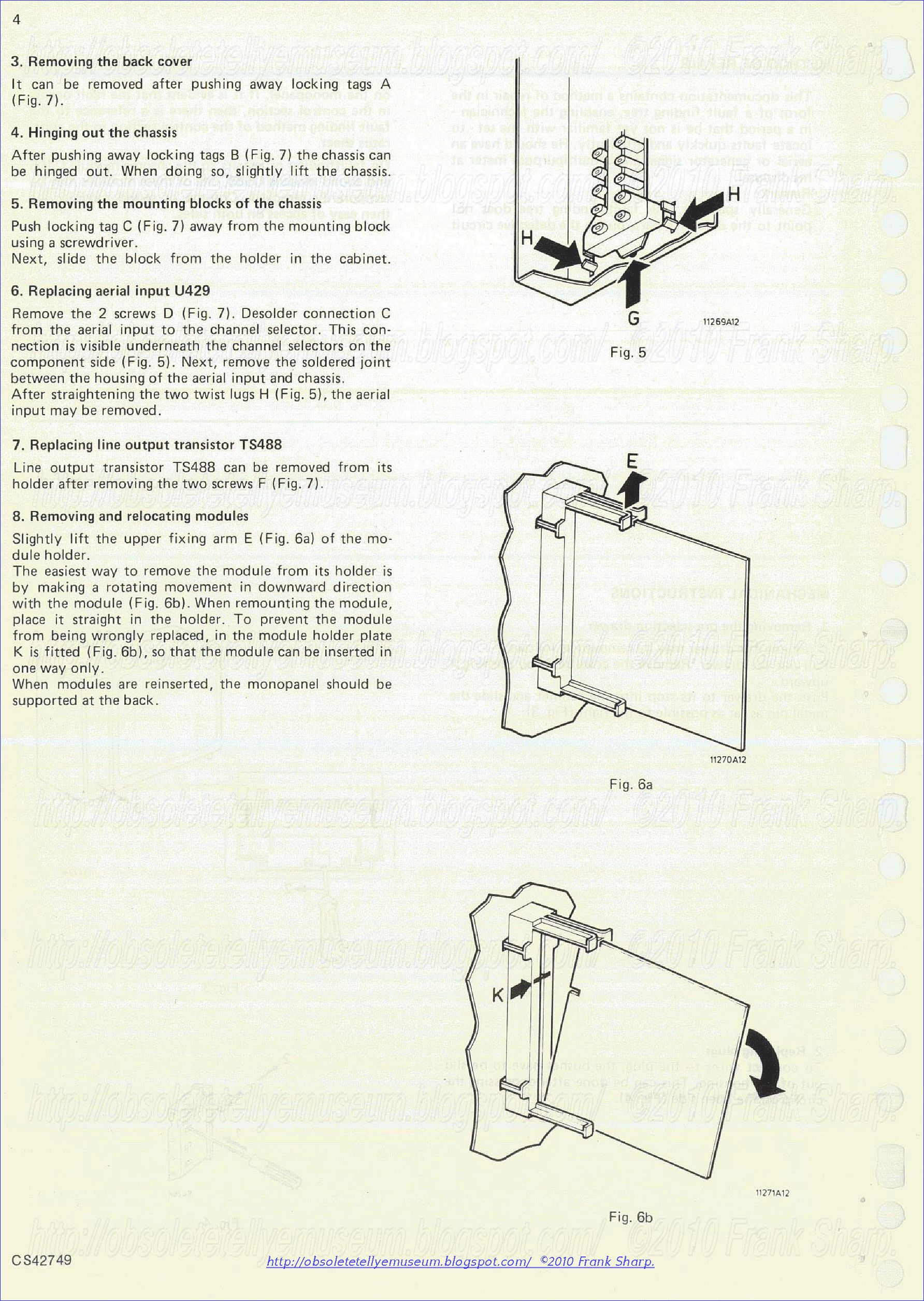


No comments:
Post a Comment
The most important thing to remember about the Comment Rules is this:
The determination of whether any comment is in compliance is at the sole discretion of this blog’s owner.
Comments on this blog may be blocked or deleted at any time.
Fair people are getting fair reply. Spam and useless crap and filthy comments / scrapers / observations goes all directly to My Private HELL without even appearing in public !!!
The fact that a comment is permitted in no way constitutes an endorsement of any view expressed, fact alleged, or link provided in that comment by the administrator of this site.
This means that there may be a delay between the submission and the eventual appearance of your comment.
Requiring blog comments to obey well-defined rules does not infringe on the free speech of commenters.
Resisting the tide of post-modernity may be difficult, but I will attempt it anyway.
Your choice.........Live or DIE.
That indeed is where your liberty lies.
Note: Only a member of this blog may post a comment.