


TUNING SYSTEM 30 PROGR. (ABSTIMMUNG BAUSTEIN 29504- 003.04)
30 Programs frequency synthesized tuning system based on SIEMENS uController and SIEMENS
synthesizer and memory.

- SDA2010 A013 uController
- SDA2112-3 (Uc controlled frequency systhesizer)
- SDA2006 (Memory x 1)
512-Bit Nonvolatile EAROM SIEMENS SDA2006 MOS circuit
General features
• Nonvolatile memory of electrical, word-organized reprogrammability, in n channel floating gate technology
• 512-bit storage capacity (32 words of 16 bits, each)
• Serial word address, chip select, and instruction input via an 8-b1t or 12-bit control word (switchable by means of external components)
• Erase and write duration determined with the aid of chip-internal control
• Signal outputs with open-drain stages active signal inputs and outputs can be inverted by terminal wiring
• Number of reprogrammings > 104
• Unlimited number of read-out procedures without refresh
• Min. 10 years storage time
Circuit description
Data transfer
Data transfer with the SDA 2006 is performed serially via a 5-line bus, consisting of:
Data input D;
Data output D q/D;;"
Data input signal REC/REC (receive data)
Clock input <P/iP
Programming output signal [/L (load)
The active input or output levels, respectively, may be inverted via the input INV. They are switchable, as a group, in order to facilitate adaptation to different external circuits.
Read-out (figure 1a and 1b)
Prior to the read operation of the memory the 8-bit or 12-bit control word must be serially clocked into the data input D. 8 or 12 clock pulses, respectively, at the input <PIP are necessary for the input of the control word. During the input, the REC/REC input is active (active high for low at INV, active low for high at INV). The information input is closed by means of the trailing edge of the REC/REC signal and at chip select the read-out instruction is decoded. In this way, also the data output D ;/D 9 becomes low-ohmic. With the aid of a further clock pulse S, the read-out operation is initialized. The data is shifted with the trailing edge of further clock pulses. The LSB arrives at the data output with the first of these pulses. During the read-out operation via the control word either the first data bit D 1 or the ninth data bit D 9 can be chosen as LSB. The read-out operation can be discontinued after any number of shift pulses. Thus.every stored 16-bit data word can also be read split into two 8-bit data words.
Reprogramming (figure 2a and 2b)
Prior to programming, the 16-bit data word (D 1 as LSB, first), then the 8-bit or 12-bit control word at the data input D; must be clocked in by means of the active REC/REC signal. It is the trailing edge of the REC/REC signal which decodes the programming instruction at chip select. The reprogramming operation, however, only starts with the trailing edge of a further clock pulse and is recorded to the memory controller via the [/L signal.
The duration tprog of reprogramming is determined by chip-internal control. Independent of the external operating voltages VpH and Vp1the erase and the write operation are only finished after every memory has reached the desired state. During rewriting, the memory cannot be influenced externally, because the input REC/REC, PIP and D; remain blocked. Premature termination of the operation can only be caused by zero level at the input RES.
Reset function
A low level voltage at the input RES moves the memory into the reset status. A voltage divider is internally connected to the input. It reliably finishes the reset status for V00 >11 V.
Voltage supply
The
SDA 2006 includes four brought out voltage inputs Vpp, Vp1, V00 , V88
with respect to Vss (ground). Normally, V00 and Vp1are externally
interconnected. The voltages VpH and Vp1 are only required during the
programming operation. During read out or in the quiescent state, they
may also be open or grounded. The values of these voltages are only of
influence on the duration, but not on the reliability of the nonvolatile
storage operation. Figure 3 shows an appropriate circuit configuration
as tuning memory in TV sets.


-----------------------------------------------------------------------------------------------------------------------
PLL Device for 125 kHz Resolution for TV Application SIEMENS SDA2112-2 Bipolar circuit
The SDA 2112-2 is fabricated in ASBC technology. In connection with a VCO (tuner) and a high-speed 1:64 divider, it forms a digitally programmable phase-locked loop for producing TV sets with PLL frequency-synthesis tuning. The PLL enables crystal-controlled setting of the tuner oscillator frequency for a 125 kHz rsolution in the frequency bands I/IIl, IV, and V.
A serial interface provides for simple connection to a microprocessor. The latter loads the programmable divider and the band-selection outputs with the appropriate information.
Features
@ No external integrator necessary
@ Internal buffer
@ Microprocessor compatible
SDA 2112-2 description (refer to block diagram) A switchable 16/17 counter is triggered by the ECL signal inputs F/F. The counter, in connection with a 4-bit and a 9-bit programmable, synchronous counter, forms a programmable, 13-bit synchronous divider using the dual-modulus technique, the 4-bit counter controlling the switchover from 16 to 17. Divider ratios of N = 256 to 8191 are possible. For test purposes the carry of the synchronous divider is available at the LDM output (open collector). The 16-bit shift register and latch is subdivided into 13 bits for storing the divider ratio N and 3 bits for controlling the three band-selection outputs. The telegram is shifted in via the serial data input IFO with the HL edge of the shift clock CPL when the enable input PLE is also on high level. First the complement of the divider ratio N, beginning with the LSB, is inserted in binary code, followed by the three control bits for the band-selection switching (see truth table). The 16-bit latch takes the data from the shift register when the enable input PLE is on low level. The IC includes a crystal-controlled, 3-MHz clock oscillator. The output signal is divided down to 1.953125 kHz (reference signal) by a 1/1536 reference divider. The oscillator frequency appears at the TTL output OSC. The clock of 62.5 kHz is available at the open-collector output CL. The divided input signal is compared with the reference signal in a digital phase detector. If the falling edge of the input signal appears prior to the falling edge of the reference signal, the DOWN output of the phase detector turns to high level for the duration of this phase difference. In the reverse case the UP output turns to high level. If the two signals are in phase, both outputs remain at low level. The UP/DOWN outputs control the two current sources I+ und! (charge pump). If the two outputs are low (PLL locked), the charge-pump output PD will turn to the high-impedance state (TRISTATE). An L signal appears at the LOCK IND output if frequency and phase are synchronous. The current sources I+ and I~ are then reduced from 300 to 100 pA. The current pulses generated by the charge pump are integrated to form the tuning voltage by means of an active lowpass filter (external pull-up resistor to supply Vso and external RC circuitry). The dc output signal appears at Viy, and serves as a tuning voltage for the VCO. The band-selection outputs (UHF, VHF, Bd I/II) contain current drains with open collectors. In this way PNP transistors working as band-selection switches can be connected directly without current-limiting resistors (see application circuit).


----------------------------------------------------------------------------------------------------------------------------------------
Application-Oriented Single Chip Microcomputer SIEMENS SDA2010 MOS circuit.
Features
@ 8 bit CPU, ROM, RAM, IN/OUT in a DIP 40 package
@ 4 analog outputs with 6 bit resolution
@ 30 digital IN/OUT lines
Two serial interfaces
Two 8 bit interfaces
Two 4 bit interfaces
Two test inputs
2 Kbyte ROM
64 byte RAM
10 ps cycle time — 1 or 2 cycles per instruction
Zero passage detector
Interface for mudulated digital signal
Interval timer/counter
5 V supply voltage
Instructions - subset of SAB 8048
Brief description
The SDA 2010 stresses application-specific control functions surpassing the former purely numeric computation performance. As a result, the use of additional hardware could be reduced and software operations have been simplified, optimizing cost savings during the developmental and production stages. Although the SDA 2010 was designed for electronic entertainment devices, it is equally suitable for mass-produced applications requiring highly economic components. The SDA 2010 includes a 2 Kbyte program memory (ROM), a 64 byte data memory (RAM) and four 6 bit D/A converters. The 30 digital IN/OUT lines are comprised of two 4 and 8 bit ports each, two test inputs and 2 serial interfaces consisting of one data and one clock line each. Test input TO processes signals modulated with approx. 30 kHz and is equipped with a digitai demoduiator, which derives the enveiope curve from the moduiaied digiiai signal. Since the digital demodulator forwards an unmodulated signal without changing it, test input TO can also function as a normal digital input during operations with standard H/L levels. Test input T1 includes a zero passage detector and can also serve as a normal digital input. The SDA 2010 is equipped with its own oscillator and timer/counter.
The instruction set includes 65 instructions (1-2 bytes), which can be processed in max. 2 cycles. Numerical problems can be processed in either binary or BCD arithmetic modes. The large number of available bit-handling instructions increases the efficiency of the controller functions. The program development and system testing for the SDA 2010 are carried out on the SME development system in conjunction with the SDA 2010 emulator board EMB U2. The EMB U2 emulator consists of one 2 K EPROM (SAB 2716) as well as a 40 pin plug which is used to insert an SAB 8035 type microprocessor or an ICE 48 plug. In addition, the EBM U2 contains all the necessary hardware to simulate the four analog outputs and the serial and parallel interfaces of the SDA 2010. A 40 wire cable is used to connect the U2 emulator with the user system. A version without the ROM (SDA 3010) is available for in-house software development on an SME system. Technical data of the SDA 2010
Maximum ratings must carefully be observed to prevent the IC from being permanently
damaged.


Siemens Digital Tuning System SDA200
Description of the system
A digital tuning system essentially consists of 3 blocks. Frequency synthesis Controller and display Station memory
Frequency synthesis
The desired frequencies are generated according to the PLL principle (Fig. 2). The PLL
comprises a VCO {the equivalent tuner oscillator), a prescaler with fixed divider factor P, a
divider with digitally selectable divider factor N, a phase detector, and an integrator. The
reference frequency for the phase detector can be obtained from a crystal oscillator with
following divider {divider factor Q).

The selection of the parameter is as follows: 1. VCO frequency range fosc. min· fosc. max• 2. Necessary frequency raster Llf 3. Max. permissible tuning time and noise phase shift. In TV applications a frequency raster of Llf = 125 kHz is sufficient. Therefore it follows that N _ fosc. min and N fosc. max min - Llf max= j f Hence a 13 bit programmable divider N = 2 ...... 8191 is required. The reference frequency fret decisively determines the tuning time and the noise phase shift of the oscilla- Llf tor. It results from the frequency raster Llfand the prescaler factor P: fret= p. On the other hand, the prescaler factor P determines the max. input frequency for the pro- grammable divider f.1max = fosc. p max · The reference frequency fret is obtained from an oscillator fref = ~ . Hence, it follows: fosc = p~ · fa. In the given system P = 64, Q = 2048, and fa = 4 MHz have been determined. The reference frequency thus results in: fret = ~f = ~ = 1.953125 kHz. 1.
The prescaler SDA 2001 is an ECL divider with a fixed divider factor P = 64. The max. input frequency is 1 GHz. A broadband preamplifier with 20 dB gain and separated switchover inputs for VHF and UHF is integrated in the SDA 2001. To ensure reliable operation, the sinusoidal input voltage covering a frequency range between 80 and 1000 MHz should be V; = 20 mV. The push-pull outputs result in good noise immunity against cross talking. The output levels of 1 VPP only cause low noise radiation.
2. The PLL IC SDA 2002 The IC contains a 13 bit binary programmable synchronous divider (divider factor N = 256 ....... 8191), a 16 bit shift register, a quartz oscillator (fosc = 4 MHz) with fol- lowing divider stage (divider factor Q = 2048), and a frequency and phase sensitive digital phase detector. Together with the 3-bit information "VHF Bd I", "VHF Bd Ill" and "UHF" the divider factor N is serially mored in the 16 bit dual code into the 16 bit shift register with parallel output. First the LSB (least significant bit) is put in, at least the MSB (most s.b.) as last bit. The transition at information input (IFO) is done only during the H state of the enable input (PLE).
The infeeding is done with the L-H slope of the clock (CPL). A 16-bit buffer memory fol- lows the 16-bit shift register. The information transition into the buffer is done with the L-level of the enable input (PLE). Referred to the H-L trailing edge of the enable input only the last 16 clocks are interpreted. Possibly preceding dummy bits will not be interpreted. A clock with the frequency f = 62.5 kHz. Appears at the open collector output CL· The out- puts VHF Bd I, VHF Bd Ill, and UHF are active low current sources (open collector). The sync divider has symmetrical push-pull inputs (F, F) for ECL level. In the case of frequency and phase synchronization, an L-signal is obtained at the output LOCK IND. The phase detector can be driven with a separated supply voltage ( V 52 ). The outputs PD and Vo are connected with an RC network. Vo delivers the tuning voltage for the VCO (tuner).
3. The SDA 2003 controller


The
integrated MOS circuit, part of the frequenc synthesis tuning system,
is located be- tween the programmable divider of the PLL circuit and
both the tuning memories which electrically memorize the allocation of
the tuning information (fine tuning) and the pro- gram number. The
controller converts the tuning information into frequency information
(divider ratio). The frequency information is a binary number,
representing the divider fac- tor for the PLL divider; it is serially
transferred into the PLL. Under usual operation, only the station
selection buttons of the TV set are actuated. A fixed program address in
the tuning memory is assigned to every static on button. This program
address is intended to store the actual tuning information as well as
the pertinent channel. After actuating a station button, a program
change instruction PC is issued from the remote control receiver or from
the front-end keyboard to the controller. This instruc- tion causes the
controller to read the tuning information (fine tuning) out of the
tuning memory and to assign it to the corresponding channel; hence the
TV set is precisely tuned to the requested frequency by means of the
PLL. Setting of a not yet stored TV transmitter is done by means of the
actuating buttons: K 1 for setting of channel units digits and K 10 for
setting of channel tens digits. By means of the button K 1 the channel
number units digits 0 to 9 without carry and by means of the button K 10
the channel number tens digits can be set. After every button
operation, the concerned channel number is incremented by 1. For every
adjustment of the channel number, the controller converts this
information into frequency information (the PLL divider factor) and
provides serial output to the PLL circuit. The success of every tuning
step can be watched on the screen. In addition to that, the SDA 2003 is
designed for station search, which can also be used for setting a TV
channel. The station search is started via the setting button: Search
Start SL. Thereupon the controller sequentially issues every frequency
information contained in the internal ROM individually to the PLL
circuit. This process is automatically stopped as soon as an operating
TV broadcast station is found. This is indicated to the controller by a
pulse (active low) at the input "Search STOP", which can be derived from
line synchronization and the video signal.
Via the setting buttons "fine tuning plus FT+" and "fine tuning minus FT - " frequency de- viations from the rated frequency of the individual channel can be set in steps of 125 kHz up to 3,875 MHz and down to - 4 MHz. Frequency tuning, moreover, readjusts automati- cally every 250 ms, as soon as the proper button is pressed. Within the tuning limits men- tioned above, fine tuning runs against a stop (owerflow inhibit). After having attained it, the channel number display lights up as long as the setting button is kept pressed. The tuning information of a tuned TV broadcast station can be stored in the tuning mem- ory by actuating the store button. The SDA 2003 then serially outputs the tuning data on the output IFO. The tuning data comprises the fine tuning information and the channel number information. From the tuning information serially read into the MOS memories, it is the channel num- ber which is used for addressing the internal ROM table. Frequency information from 100TV channels as well as band selection (2 bytes) are stored in the ROM table. There are some frequencies to which several TV channels are allocated (stored in the ROM), hence no unambiguous channel designition can be gathered from the frequency. This is the reason why the channel number is used as tuning information, since only in this way unambiguous channel designation and frequency information can be gained, simul- taneously. The frequency information is obtained by adding up the ROM divider factor and the center position of fine tuning. At every process of setting a new channel number, fine tuning is adjusted to center position. The PLL divider factor then complies with the nominal divider factor. The nominal divider factor results in an oscillator frequency lying only by f = 25 kHz below the nominal value. It represents the frequency information of the exact channel frequency, except the deviation of 25 kHz which is needed to attain a 125 kHz raster frequency at a given IF of 38.9 MHz. The band selection information is programmed in the internal ROM for every frequency information and is serially output from the con- troller. Band selection differentiates between VHF range I/Ill and UHF. The internal ROM table is made up such that between the CCIR channels - designated with corresponding channel numbers - other channels are allocated. Thus, the Italian TV channels A-H are stored between channel 12 and channel 21 under channel Nos. 13 to 20. Data communication between the SDA 2003 and the memory is done via a data bus that comprises shift clock CNVM, actual information (IFO), and an enable signal (EX/REC). The data word contains information on channel number and fine tuning.
4. Display driver SDA 2004
The LED display driver decodes in the remote-controlled tuning system of TV sets the channel and program numbers from a serially offered BCD code and drives in multiplex operation 2 or 4 digits, as required. The information D (active H) for the four digits is coded in 16 bits and is serially input in two shift registers of 8 bits, each. The input for the digits D, and D, and/or D3 and D. is provided by 8 falling edges of the driving clock pulses T,, or T3•. respectively, if Enable EN is on high level. The contents of both the shift registers is stored in an eight bit broad memory, if EN is on low level. The 16 memory outputs operate on a multiplexer. The multi- plexer and the digit selection outputs Dl 1, Dl 2, Dl 3 and Dl 4 (digit driver for the LED dis- plays, active low) are serviced by an internal clock generator. The 7 outputs of the de-coder, series-connected to the multiplexer, are used for driving the segments (active high)
in the LEDs.
If input 01 4 is grounded, the multiplexer only works for the digits 1 and 2. Thereby the duty
cycle for the clock pulse of the multiplexer is changed over.
5. On-screen IC SDA 2105
The SDA 2105 IC is intended to display channel and program numbers on the screen of the TV set and is adapted to the SDA 2003 Siemens channel processor. The on-screen device provides 2 display panels of 2 digits, each, and 1 display panel of 5 digits. The information for the display panels is serially transferred via the DATA line. The display panels are activated via the pertinent ENABLE line.
6. Nonvolatile memory SDA 2006
This IC allows the nonvolatile, wordoriented reprogrammable storage of 32 x 16 bit words. Thus, up to 32 programs or channels as well as their possible allocations can be stored. The SDA 2006 is fabricated in the n-channel floating gate technology in order to provide extremely long storage times and as many read-out operations as required refresh. Addressing and instruction input is done serially and may comprise 8 or 12 bits as re- quired. The entailing erase and write cycles are determined by a complex, chip-internal control.
7. IR remote control receiver SDA 2007
The device is a further development of the types SAB 3209 and SAB 4209. Like those, it utilizes the proven biphase code for IR transmission and, therefore, it can be applied with the SAB 3210 or SDA 2008 as IR instruction generator. It is, in particular, designed for operation in connection with the tuning system SDA 200. The program memory has, there- fore, been relocated from the remote control receiver to the channel processor SDA 2003.
Particulars:
2 combined series interfaces with common DATA line for information transfer (leading bit LB = H and 6 information bits A, B, C, D, E, and F). Distinction is made by the enable signals OLE and TE (7 pulses, each, i.e. 1 pulse/bit). Modification is possible through the outputs of the TUS 1/2 flip-flops, thus different groups of equipment such as teletext de- coder and the VCR device can be addressed precisely. H level at one of the TUS outputs drops the OLE pulses (OLE = L) out and switches the TE output over to single mode operation. For a better adaptation to a microprocessor the output is now executed by means of 4 T osc/bit (64 μs/bit at 62.5 kHz).
2 combined series interfaces with common DATA line for information transfer (leading bit LB = H and 6 information bits A, B, C, D, E, and F). Distinction is made by the enable signals OLE and TE (7 pulses, each, i.e. 1 pulse/bit). Modification is possible through the outputs of the TUS 1/2 flip-flops, thus different groups of equipment such as teletext de- coder and the VCR device can be addressed precisely. H level at one of the TUS outputs drops the OLE pulses (OLE = L) out and switches the TE output over to single mode operation. For a better adaptation to a microprocessor the output is now executed by means of 4 T osc/bit (64 μs/bit at 62.5 kHz).
During the "standby" status (ON/OFF = H), all outputs of the 4 analog memories VOLU, BRIG, COLO and CONT are kept on L level. Corrective instructions (instruction Nos. 8 to 15) will then not be executed, i.e. the last set status of the analog memories is retained. The connection VPM, included in the volume memory VOLU, is provided for front end con- trolling, which acts like the instructions "volume+" and "volume-", respectively. 2 spare outputs, controlled by 2 alternating flip-flops with different quiescent levels open up additional individual applications (e.g. clock time display).
There is, moreover, the possibility to switch over the start bit for IR reception. Thus, two
receiver units can be operated in the same room at the same clock frequency indepen-
dently of each other.
8. Remote control transmitter SDA 2008
The transmitter module SDA 2008 is an advanced product of the SAB 3210 IC within the
frame of the IR 60 Siemens infrared remote control system. In detail,the IC includes the
following:
1. The keyboard is completely latched against incorrect operation. Even in case of double operation as provided for instruction input within one column with one of the lines 1 to 7 incl. line 8, practically no misinstruction can be generated by pressing two buttons, since for that both the buttons had to be pressed absolutely simultaneously.
2. After outputting the first information instruction, the instruction can only be changed by switching off the transmitter (releasing all buttons). This avoids further incorrect ser- vicing because no unwanted instruction change can be effected by premature releasing the "shift button" (keyboard changeover) or pressing a further button.
3. Instruction expansion to more than 32 instructions can be done as previously by diode wiring, and recently additionally via a "shift button" (connects PPIN to SA). Moreover, the instructions 40 to 47 can be issued by connecting the line inputs to - Vs without re- quiring any additional component.
4. The start bit in infrared transmission can be changed over from outside (connecting PPIN to SC). Thus, selective addressing of 2 different receivers by one transmitter is possible. A TV transmitter and a broadcasting set with one transmitter can, therefore, be serviced independently of each other in one room.
5. The oscillator was converted to 8 times the frequency in order to permit operation with a ceramic resonator. Hence, also lowcost AM IF resonators (appr. 500 kHz or 455 kHz) can be used instead of the oscillator.
6. In addition to the hitherto existing final instruction, an "initial instruction" is transmit- ted. The initial instruction exactly complies with the final instruction, except that it is issued by information instructions. Thus separation between 2 button operations can be recognized even more precisely, and more time is provided for the gain control of the preamplifiers on the receiver side.
7. No external column resistors are required.
TDA1905 5W AUDIO AMPLIFIER WITH MUTING.DESCRIPTION
The TDA1905 is a monolithic integrated circuit in
POWERDIP package, intended for use as low
frequency power amplifier in a wide range of applications
in radio and TV sets:
– muting facility
– protection against chip over temperature
– very low noise
– high supply voltage rejection
– low ”switch-on” noise
– voltage range 4V to 30V
The TDA 1905 is assembled in a new plastic package,
thePOWERDIP, that offers the same assembly
ease, space and cost saving of a normal dual in-line
packagebutwith apower dissipationofup to6Wand
a thermal resistance of 15°C/W (junction to pins).
THERMAL SHUT-DOWN
The presence of a thermal limiting circuit offers the following advantages:
1) An overload on the output (even if it is permanent), or an above limit ambient temperature can be easily
tolerated since the Tj cannot be higher than 150 °C.
2) The heatsink can have a smaller factor of safety compared with that of a conventional circuit. There is
no possibility of device damage due to high junction temperature.
If for any reason, thejunction temperatureincreases upto 150°C, the thermalshut-down simply reduces
the power dissipation and the current consumption.
The maximum allowable power dissipation depends upon the size of the external heatsink (i.e. its thermal
resistance).
- TUA2000 (SIEMENS) OSC+ MIXER
- TDA5500 (SIEMENS) IF VIDEO
- TBA120T (TELEFUNKEN) IF AUDIO

TBA120T (Siemens) SIF (Sound IF)
VIDEO + RGB UNIT (FARB BAUSTEIN 29504-005... )
TDA3561A (PHILIPS) Luminance+Chrominance+RGB MATRIX

PAL decoder TDA3561A
GENERAL DESCRIPTION
The TDA3561A is a decoder for the PAL colour television standard. It combines all functions required for the identification
and demodulation of PAL signals.
Furthermore it contains a luminance amplifier, an RGB-matrix and amplifier. These
amplifiers supply output signals up to 5 V peak-to-peak (picture information) enabling direct drive of the discrete output
stages.

The circuit also contains separate inputs for data insertion, analogue as well as digital, which can be used for text display systems (e.g. (Teletext/broadcast antiope), channel number display, etc. Additional to the TDA3560, the
circuit includes the following features:
· The peak white limiter is only active during the time that the 9,3 V level at the output is exceeded.
The start of the
limiting function is delayed by one line period. This avoids peak white limiting by test patterns which have abrupt transitions from colour to white signals.
· The bri
ghtness control is obtained by inserting a variable pulse in the luminance channel. Therefore the ratio of brightness variation and signal amplitude at the three outputs will be identical and independent of the difference in gain of the three channels. Thus discolouring due to adjustment of contrast and brightness is avoided.· Improved suppression of the internal RGB signals when the device is switched to external signals, and vice versa.
· Non-synchronized external RGB signals do not disturb the black level of the internal signals.
· Improved suppression of the residual 4,4 MHz signal in the RGB output stages.
· Cascoded stages in the demodulators and burst phase detector minimize the radiation of the colour demodulator
inputs.
· High current capability of the RGB outputs and the chrominance output.
APPLICATION INFORMATION
The function is described against the corresponding pin
number.
1. + 12 V power supply
The circuit gives good operation in a supply voltage range
between 8 and 13,2 V provided that the supply voltage for
the controls is equal to the supply voltage for the
TDA3561A. All signal and control levels have a linear
dependency on the supply voltage. The current taken by
the device at 12 V is typically 85 mA. It is linearly
dependent on the supply voltage.
2. Control voltage for identification
This pin requires a detection capacitor of about 330 nF for
correct operation. The voltages available under various
signal conditions are given in the specification.
3. Chrominance input
The chroma signal must be a.c.-coupled to the input.
Its amplitude must be between 55 mV and 1100 mV
peak-to-peak (25 mV to 500 mV peak-to-peak burst
signal).
 All figures for the chroma signals are based on a
colour bar signal with 75% saturation, that is the
burst-to-chroma ratio of the input signal is 1 : 2,25.
4. Reference voltage A.C.C. detector
This pin must be decoupled by a capacitor of about 330
nF. The voltage at this pin is 4,9 V.
5. Control voltage A.C.C.
The A.C.C. is obtained by synchronous detection of the
burst signal followed by a peak detector. A good noise
immunity is obtained in this way and an increase of the
colour for weak input signals is prevented. The
recommended capacitor value at this pin is 2,2 µF.
6. Saturation control
The saturation control range is in excess of 50 dB.
The control voltage range is 2 to 4 V. Saturation control is
a linear function of the control voltage.
When the colour killer is active, the saturation control
voltage is reduced to a low level if the resistance of the
external saturation control network is sufficiently high.
Then the chroma amplifier supplies no signal to the
demodulator. Colour switch-on can be delayed by proper
choice of the time constant for the saturation control
setting circuit.
When the saturation control pin is connected to the power
supply the colour killer circuit is overruled so that the colour
signal is visible on the screen. In this way it is possible to
adjust the oscillator frequency without using a frequency
counter (see also pins 25 and 26).
7. Contrast control
The contrast control range is 20 dB for a control voltage
change from + 2 to + 4 V. Contrast control is a linear
function of the control voltage. The output signal is
suppressed when the control voltage is 1 V or less. If one
or more output signals surpasses the level of 9 V the peak
white limiter circuit becomes active and reduces the out
putsignals via the contrast control by discharging C2 via an
internal current sink.
8. Sandcastle and field blanking input
The output signals are blanked if the amplitude of the input
pulse is between 2 and 6,5 V. The burst gate and clamping
circuits are activated if the input pulse exceeds a level of
7,5 V.
The higher part of the sandcastle pulse should start just
after the sync pulse to prevent clamping of video signal on
the sync pulse. The width should be about 4 µs for proper
A.C.C. operation.
9. Video-data switching
The insertion circuit is activated by means of this input by
an input pulse between 1 V and 2 V. In that condition, the
internal RGB signals are switched off and the inserted
signals are supplied to the output amplifiers. If only normal
operation is wanted this pin should be connected to the
negative supply. The switching times are very short
(< 20 ns) to avoid coloured edges of the inserted signals
on the screen.
10. Luminance signal input
The input signal should have a peak-to-peak amplitude of
0,45 V (peak white to sync) to obtain a black-white output
signal to 5 V at nominal contrast. It must be a.c.-coupled to
the input by a capacitor of about 22 nF. The signal is
clamped at the input to an internal reference voltage.
A 1 kΩ luminance delay line can be applied because the
luminance input impedance is made very high.
Consequently the charging and discharging currents of the
coupling capacitor are very small and do not influence the
signal level at the input noticeably. Additionally the
coupling capacitor value may be small.
11. Brightness control
The black level of the RGB outputs can be set by the
voltage on this pin (see Fig.5). The black level can be set
higher than 4 V however the available output signal
amplitude is reduced (see pin 7). Brightness control also
operates on the black level of the inserted signals.
12, 14, 16. RGB outputs
The output circuits for red, green and blue are identical.
Output signals are 5,25 V (R, G and B) at nominal input
signals and control settings. The black levels of the three
outputs have the same value. The blanking level at the
outputs is 2,1 V. The peak white level is limited to 9,3 V.
When this level exceeded the output signal amplitude is
reduced via the contrast control (see pin 7).
13, 15, 17. Inputs for external RGB signals
The external signals must be a.c.-coupled to the inputs via
a coupling capacitor of about 100 nF. Source impedance
should not exceed 150 Ω. The input signal required for
a 5 V peak-to-peak output signal is 1 V peak-to-peak.
At the RGB outputs the black level of the inserted signal is
identical to that of normal RGB signals. When these inputs
are not used the coupling capacitors have to be connected
to the negative supply.
18, 19, 20. Black level clamp capacitors
The black level clamp capacitors for the three channels are
connected to these pins. The value of each capacitor
should be about 100 nF.
21, 22. Inputs (B-Y) and (R-Y) demodulators
The input signal is automatically fixed to the required level
by mean
s of the burst phase detector and A.C.C.generator which are connected to pin 21 and pin 22. As the
burst (applied differentially to those pins) is kept constant
by the A.C.C., the colour difference signals automatically
have the correct value.
23, 24. Burst phase detector outputs
At these pins the output of the burst phase detector is
filtered and controls the reference oscillator. An adequate
catching range is obtained with the time constants given in
the application circuit (see Fig.6).
25, 26. Reference oscillator
The frequency of the oscillator is adjusted by the variable
capacitor C1. For frequency adjustment interconnect pin
21 and pin 22. The frequency can be measured by
connecting a suitable frequency counter to pin 25.
28. Output of the chroma amplifier
Both burst and chroma signals are available at the output.
The burst-to-chroma ratio at the output is identical to that
at the input for nominal control settings. The burst signal is
not affected by the controls. The amplitude of the input
signal to the demodulator is kept constant by the A.C.C.
Therefore the output signal at pin 28 will depend on the
signal loss in the delay line.
- U264B (TELEFUNKEN) PRESCALER (Under the screen in the middle of PCB)
ABLENKUNG 90° 29504-007.21 TDA2594 HORIZONTAL COMBINATIONThe TDA2594 is a monolithic integrated circuit intended for use in colour television receivers.
The circuit incorporates the following functions:
0 Horizontal oscillator based on the threshold switching principle.
0 Phas
e comparison between sync pulse and oscillator voltage (tp1).0 Internal key pulse for phase detector (-D) fYP~ ‘I V
V3-1elp-pl WP- 1° V
* Permissible range: 1 t
TDA2653A Vertical deflection circuit
DESCRIPTION
The TDA2653A is a monolithic integrated circuit for vertical deflection in large screen colour television receivers.
The circuit incorporates the following functions:
· Oscillator; switch capability for 50 Hz/60 Hz operation
· Synchronization circuit
· Blanking pulse generator with guard circuit
· Sawtooth generator with buffer stage
· Preamplifier with fed-out inputs
· Output stage with thermal and short-circuit protection
· Flyback generator
· Voltage stabilizers
PINNING
1. Oscillator adjustment
2. Synchronization input/blanking output
3. Sawtooth generator output
4. Preamplifier input
5. Positive supply of output stage
6. Output
7. Flyback generator output
8. Ground
9. Positive supply (VS)
10. Reference voltage
11. Sawtooth capacitor
12. 50 Hz/ 60 Hz switching voltage
13. Oscillator capacitor.
APPLICATION INFORMATION
The function is described against the corresponding pin number
1, 13. Oscillator
The oscillator frequency is determined by a potentiometer at pin 1 and a capacitor at pin 13.
2. Sync input/blanking output
Combination of sync input and blanking output. The oscillator has to be synchronized by a positive-going
pulse between 1 and 12 V. The integrated frequency detector delivers a switching level at pin 12.
The blanking pulse amplitude is 20 V with a load of 1 mA.
3. Sawtooth generator output
The sawtooth signal is fed via a buffer stage to pin 3. It delivers the signal which is used for linearity control,
and drive of the preamplifier. The sawtooth is applied via a shaping network to pin 11 (linearity) and via a
resistor to pin 4 (preamplifier).
4. Preamplifier input
The DC voltage is proportional to the output voltage (DC feedback). The AC voltage is proportional to the
sum of the buffered sawtooth voltage at pin 3 and the voltage, with opposite polarity, at the feedback
resistor (AC feedback).
5. Positive supply of output stage
This supply is obtained from the flyback generator. An electrolytic capacitor between pins 7 and 5, and a
diode between pins 5 and 9 have to be connected for proper operation of the flyback generator.
6. Output of class-B power stage
The vertical deflection coil is connected to this pin, via a series connection of a coupling capacitor and a
feedback resistor, to ground.
7. Flyback generator output
An electrolytic capacitor has to be connected between pins 7 and 5 to complete the flyback generator.
8. Negative supply (ground)
Negative supply of output stage and small signal part.
9. Positive supply
The supply voltage at this pin is used to supply the flyback generator, voltage stabilizer, blanking pulse
generator and buffer stage.
10. Reference voltage of preamplifier
External adjustment and decoupling of reference voltage of the preamplifier.
11. Sawtooth capacitor
This sawtooth capacitor has been split to realize linearity control.
12. 50 Hz/60 Hz switching level
This pin delivers a LOW voltage level for 50 Hz and a HIGH voltage level for 60 Hz. The amplitudes of the
sawtooth signals can be made equal for 50 Hz and 60 Hz with these levels.
NF BAUSTEIN 29504-004.22
ABLENKUNG 90° 29504-007.21
TUNER 20504-001.03
Tone Control IC TDA 4290-2
TDA 4290-2 SBipolar IC
Tone control lC for the DC voltage control of volume, treble, and bass. The volume characteristic
can be changed from linear to physiological.
For mono application we recommend the TDA 4290-2, while the TDA 4290-2 S is especially
suitable for stereo application.
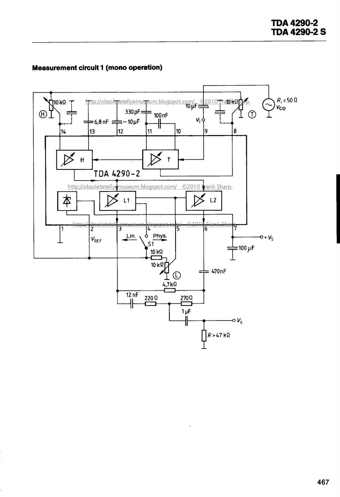
O Few external components
Q High signal-to-noise ratio
O Low total harmonic distortion
O Complies with the IEC 268-3 standards
Maximum ratings
Supply voltage VS 18 V
Control inputs V5, V8, V14 O to Vs V
Input signal V8,,“ 3 V
Load current I2 10 mA
Junction temperature 7] 150 °C
Storage temperature range Tm -40 to 125 “C
Thermal resistance (system-air) Rm SA 90 K/W
Operating range
Supply voltage VS 10.5 to 18 V
Volume control V5 0 to 0.51 x V2 V
Frequency (—1 dB) fi 20 to 20,000 Hz
Ambient temperature TA O to 70 °C
No comments:
Post a Comment
The most important thing to remember about the Comment Rules is this:
The determination of whether any comment is in compliance is at the sole discretion of this blog’s owner.
Comments on this blog may be blocked or deleted at any time.
Fair people are getting fair reply. Spam and useless crap and filthy comments / scrapers / observations goes all directly to My Private HELL without even appearing in public !!!
The fact that a comment is permitted in no way constitutes an endorsement of any view expressed, fact alleged, or link provided in that comment by the administrator of this site.
This means that there may be a delay between the submission and the eventual appearance of your comment.
Requiring blog comments to obey well-defined rules does not infringe on the free speech of commenters.
Resisting the tide of post-modernity may be difficult, but I will attempt it anyway.
Your choice.........Live or DIE.
That indeed is where your liberty lies.
Note: Only a member of this blog may post a comment.