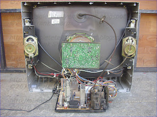
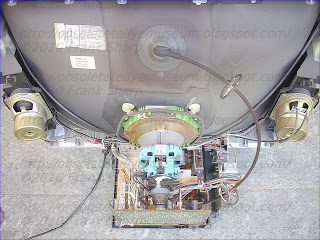
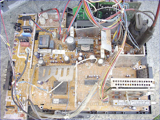
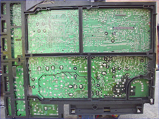
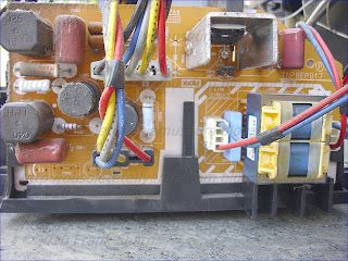
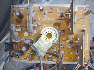
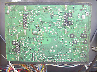
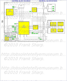
PANASONIC TX-29AS10C CHASSIS EURO-4H : This is a Full Digital Chassis.
The PANASONIC EURO- 4H is developing the 100HZ DIGITAL SCAN RATE TECHNOLOGY WITH ITT/MICRONAS DIGIT.3000 CHIPSET FAMILY.
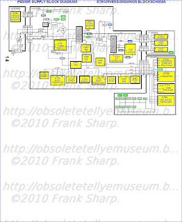
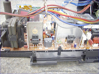
This chassis was reliable except for a high rate of various faults caused by dry joints around the chassis but expecially concentrated in the digital board box featuring all digital video functions.
These fault were mainly caused because the chipset is running discretely warm and for that developing spurious faults landing in fuzzy behaviours of the tellye itself.
A complete PROFESSIONAL REWORKING EXECUTION of the aforementioned digital unit was solving all problems definitely.
PANASONIC TX-29AS10C CHASSIS EURO-4H CIRCUITS DESCRIPTIONS:

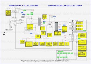
STRF6654LF51 OFF-LINE QUASI-RESONANT FLYBACK SWITCHING REGULATORS:
The Series STR-F6600 is specifically designed to satisfy the require-
ments for incre
 ased integration and reliability in off-line quasi-resonant
flyback converters. The series incorporates a primary control and drive
circuit with discrete avalanche-rated power MOSFETs.
Covering the power range from below 25 watts up to 300 watts for
100/115/230 VAC inputs, and up to 150 watts for 85 to 265 VAC
universal input, these devices can be used in a range of applications,
from battery chargers and set top boxes, to televisions, monitors, and
industrial power supply units.
Cycle-by-cycle current limiting, under-voltage lockout with hyster-
esis, over-voltage protection, and thermal shutdown protects the power
supply during the normal overload and fault conditions. Over-voltage
protection and thermal shutdown are latched after a short delay. The
latch may be reset by cycling the input supply. Low-current startup and
a low-power standby mode selected from the secondary circuit completes
a comprehensive suite of features. The series is provided in a five-pin
overmolded TO-3P style package, affording dielectric isolation without
compromising thermal characteristics.
FEATURES
I Flyback Operation with Quasi-Resonant Soft Switching
for Low Power Dissipation and EMI
I Rugged Avalanche-Rated MOSFET
I Choice of MOSFET Voltage and rDS(on)
I Full Over-Current Protection (no blanking)
I Under-Voltage Lockout with Hysteresis
I Over-Voltage Protection
I Direct Voltage Feedback
I Low Start-up Current (<400 br=""> I Low-Frequency, Low-Power Standby Operation
I Overmolded 5-Pin Package.
LA7845 Vertical Deflection Output Circuit:
Overview
The LA7845 is a vertical deflection output IC for high-
resolution television and CRT display systems that use a
bus controller system signal processing IC. It can directly
drive the deflection yoke (including the required DC
component) from the bus controller system signal
processing IC's sawtooth waveform output. Connecting
the LA7845 and a Sanyo TV bus control system signal
processing IC in th
 e LA7615 series allows all functions of
a color television signal system to be processed by the bus
system. Since the LA7845 has a maximum deflection
current of 2.2 Ap-p, it is optimal for use in large aperture
products, and is capable of driving 33 to 37 inch class
monitors.
Features
• Low power dissipation due to the provision of a built-in
pump circuit
• Vertical output circuit
• On-chip thermal protection circuit
• Good crossover characteristics
• Supports DC coupling.
PHILIPS TDA6111Q Video output amplifier:
GENERAL DESCRIPTION
The T
 DA6111Q is a video output amplifier with 16 MHz
bandwidth. The device is contained in a single in-line 9-pin
medium power (DBS9MPF) package, using high-voltage
DMOS technology, intended to drive the cathode of a
colour CRT.
FEATURES
• High bandwidth and high slew rate
• Black-current measurement output for Automatic
Black-current Stabilization (ABS)
• Two cathode outputs; one for DC currents, and one for
transient currents
• A feedback output separated from the cathode outputs
• Internal protection against positive appearing
Cathode-Ray Tube (CRT) flashover discharges
• ESD protection
• Simple application with a variety of colour decoders
• Differential input with a designed maximum common
mode input capacitance of 3 pF, a maximum differential
mode input capacitance of 0.5 pF and a differential input
voltage temperature drift of 50 µV/K
• Defined switch-off behaviour.
Cathode output
The cathode output is protected against peak currents
(caused by positive voltage peaks during high-resistance
flash) of 5 A maximum w
 ith a charge content of 100 µC.
The cathode is also protected against peak currents
(caused by positive voltage peaks during low-resistance
flash) of 10 A maximum with a charge content of 100 nC.
Flashover protection
The TDA6111Q incorporates protection diodes against
CRT flashover discharges that clamp the cathode output
pin to the VDDH pin. The DC supply voltage at the VDDH pin
has to be within the operating range of 180 to 210 V to
ensure that the Absolute Maximum Rating for VDDH of
250 V will not be exceeded during flashover. To limit the
diode current, an external 680 Ω carbon high-voltage
resistor in series with the cathode output and a 2 kV spark
gap are needed (for this resistor-value, the CRT has to be
connected to the main PCB). This addition produces an
increase in the rise and fall times of approximately 5 ns
and a decrease in the overshoot of approximately 4%.
VDDH to GND must be decoupled:
1.
With a capacitor >20 nF with good HF behaviour
(e.g. foil). This capacitance must be placed as close
as possible to pins 6 and 4, but definitely within 5 mm.
2.
With a capacitor >10 µF on the picture tube base print
(common for three output stages).
VDDL to GND must be decoupled:
1.

With a capacitor >20 nF with good HF behaviour
(e.g. ceramic). This capacitance must be placed as
close as possible to pins 2 and 4, but definitely within
10 mm.
Switch-off behaviour
The switch-off behaviour of the TDA6111Q is defined:
when the bias current becomes zero, at VDDL (pin 2) lower
than approximately 5 V, all the output pins
(pins 7, 8 and 9) will be high.
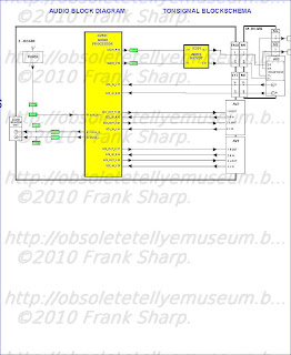
MSP3400C
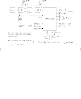
Multistandard Sound Processor
Release Notes: The hardware description in this
document is valid for the MSP 3400C – C8 and newer
codes. Revision bars indicate significant changes
to the previous version.
1. Introduction
The MSP 3400C is designed as single-chip Multistandard
Sound Processor for applications in analog and
digital TV sets, satellite receivers and video recorders.
The MSP-family, which is based on the MSP 2400, demonstrates
the progressive development towards highly
integrated multi-functional ICs.
The MSP 3400C, again, improves function integration:
The full TV sound processing, starting with analog
sound IF signal-in, down to processed analog AF-out, is
performed in a single chip. The IC is produced in 0.8 mm
CMOS technology, combined with high performance
digital signal processing.
The MSP 3400C 0.8 m CMOS version is fully pin and
software compatible to the 1.0 m MSP 3400 and MSP
3410. The main difference between the MSP 3400C and
the MSP 3410, consists of the MSP 3410 being able to
decode NICAM signals.
2. Features of the MSP 3400C:
2.1. Features of the Demodulator and Decoder
Sections
The MSP 3400C is designed to perform demodulation
of FM-mono TV sound and two carrier FM systems according
to the German or Korean terrestrial specs. With
certain constraints, it is also possible to do AM-demodulation
according to the SECAM system. Alternatively, the
satellite specs can be processed with the MSP 3400C.
For FM carrier detection in satellite operation, the AMdemodulation
offers a powerful feature to calculate the
carrier field strength, which
 can be used for automatic
search algorithms. So, the IC facilitates a first step towards
multistandard capability with its very flexible
application and may be used in TV-sets, satellite tuners,
and video recorders.
The MSP 3400C facilitates profitable multistandard capability,
offering the following advantages:
– two selectable analog inputs (TV and SAT-IF sources)
– Automatic Gain Control (AGC) for analog input: input
range: 0.14 – 3 Vpp
– integrated A/D converter for sound-IF inputs
– all demodulation and filtering is performed on chip and
is individually programmable
– no external filter hardware is required
– only one crystal clock (18.432 MHz) is necessary
– FM carrier level calculation for automatic search algorithms
and carrier mute function
– high deviation FM-mono mode (max. deviation:
approx. 360 kHz)
2.2. Features of the DSP-Section
– flexible selection of audio sources to be processed
– digital input and output interfaces via I2S-Bus for external
DSP-processors, surround sound, ADR etc.
– digital interface to process ADR (Astra Digital Radio)
together with DRP 3510 A
– performance of all deemphasis systems including
adaptive Wegener Panda 1 without external components
or controlling
– digitally performed FM-identification decoding and dematrixing
– digital baseband processing: volume, bass, treble,
5-band equalizer, loudness, pseudostereo, and basewidth
enlargement
– simple controlling of volume, bass, treble, equalizer
etc.
– increased audio bandwidth for FM-Audio-signals
(20 Hz – 15 kHz, 1 dB)
2.3. Features of the Analog Section
– three selectable analog pairs of audio baseband inputs
(= three SCART inputs)
input level: 32 V RMS,
input impedance: .25 kW
– one selectable analog mono input (i.e. AM sound),
input level: 32 V RMS,
input impedance: .10 kW
– two high quality A/D converters, S/N-Ratio: .85 dB
– 20 Hz to 20 kHz Bandwidth for SCART-to-SCARTCopy
facilities
– MAIN (loudspeaker) and AUX (headphones): two
pairs of 4-fold oversampled D/A-converters
output level per channel: max. 1.4 V RMS
output resistance: max. 5 kW
S/N-Ratio: .85 dB at maximum volume
max. noise voltage in mute mode: 310 mV (BW: 20 Hz
...16 kHz)
– one pair of four-fold oversampled D/A-converters supplying
two selectable pairs of SCART-Outputs. Output
level per channel: max. 2 V RMS, output resistance:
max. 0.5 kW, S/N-Ratio: .85 dB
(20 Hz...16 kHz).
-----------------------------------------------------------------------
DIGITAL BOARD CIRCUITS DESCRIPTIONS.

SDA 9401 SCARABAEUS Scan Rate Converter using Embedded DRAM Technology Units:
General description
The SDA 9401 is a new component of the Micronas MEGAVISION® IC set in a 0.35 µm embedded
DRAM technology (field memory embedded). The SDA 9401 is pin compatible to the SDA 9400
(frame memory embedded). The SDA 9401 comprises all main functionalities of a digital featurebox
in one monolithic IC.
The SDA 9401 does a simple 100/120 Hz interlaced (50/60 Hz progressive) scan rate conversion.
The scan rate converted picture can be vertically expanded. The SDA 9401 has a freerunning
mode, therefore features like multiple picture display (e.g. tuner scan) are possible.
The noise reduction is field based. Furthermore separate motion detectors for luminance and
chrominance have been implemented. For automatic controlling of the noise reduction parameters a
noise measurement algorithm is included, which measures the noise level in the picture or in the
blanking period. In addition a spatial noise reduction is implemented, which reduces the noise even
in the case of motion. The input signal can be compressed horizontally and vertically with a certain
number of factors. Therefore split screen modes are supported too.
Beside these additional functions like coloured background, windowing and flashing are
implemented.
2 Features
• Two input data formats
- 4:2:2 luminance and chrominance parallel (2 x 8 wires)
- ITU-R 656 data format (8 wires)
• Two different represen
 tations of input chrominance data
- 2‘s complement code
- Positive dual code
• Flexible input sync controller
• Flexible compression of the input signal
- Digital vertical compression of the input signal (1.0, 1.25, 1.5, 1.75, 2.0, 3.0, 4.0)
- Digital horizontal compression of the input signal (1.0, 2.0, 4.0)
• Noise reduction
- Motion adaptive spatial and temporal noise reduction (3D-NR)
- Temporal noise reduction for luminance field based
- Temporal noise reduction for chrominance field based
- Separate motion detectors for luminance and chrominance
- Flexible programming of the temporal noise reduction parameters
- Automatic measurement of the noise level (5 bit value, readable by I²C bus)
• TV mode detection by counting line numbers (PAL, NTSC, readable by I²C bus)
• Embedded memory
- 3.2 Mbit embedded DRAM core for field memories
- 128 kbit embedded DRAM core for line memories.
• Flexible clock and synchronization concept
- Decoupling of the input and output clock system possible
• Scan rate conversion
- Simple 100/120 Hz interlaced scan conversion (e.g. AABB, AA*B*B)
- Simple progressive scan conversion (e.g. AA*)
• Flexible digital vertical expansion of the output signal (1.0, ... [1/32] ... , 2.0)
• Flexible output sync controller
- Flexible positioning of the output signal
- Flexible programming of the output sync raster
• Signal manipulations
- Insertion of coloured background
- Vertical and/or horizontal windowing with four different speed factors
- Flash generation
- Still field
- Support of split screen applications
- Multiple picture display - Tuner scan (4 and 16 times for 4:3, 12 times for 16:9 tubes)
- Support of multi picture display with PIP or front-end processor with integrated scaler
(e.g. 9 times display of PIP pictures, picture tracking, random pictures,
still-in-moving picture, moving-in-still picture)
• I²C-bus control (400 kHz).
VPC 3215C Video Processor Family

The VPC 32x5 is a high-quality, single-chip video
front-end, which is targeted for 4:3 and 16:9, 50/60 and
100/120 Hz TV sets. It can be combined with other
members of the DIGIT3000 IC family (such as CIP
3250A, DDP 3300A, TPU 3040) and/or it can be used
with 3rd-party products.
The main features of the VPC 32x5 are
– all-digital video processing
– high-performance adaptive 4H comb filter Y/C separator
with adjustable vertical peaking
– multi-standard color decoder PAL/NTSC/SECAM
including all substandards
– 4 composite, 1 S-VHS input, 1 composite output
– integrated high-quality A/D converters and associated
clamp and AGC circuits
– multi-standard sync processing
– linear horizontal scaling (0.25 ... 4), as well as
non-linear horizontal scaling ‘panorama vision’
– PAL+ preprocessing (VPC 3215)
– line-locked clock, data and sync output (VPC 3215)
– display/deflection control (VPC 3205)
– submicron CMOS technology
– I2C-Bus Interface
– one 20.25 MHz crystal, few external components
– 68-pin PLCC package
1.1. System Architecture
Fig. 1–1 shows the block diagram of the video processor.
1.2. Video Processor Family
The VPC video processor family supports 15/32 kHz
systems and is available with different comb filter
options. The 50 Hz/single scan versions provide controlling
for the display and the vertical/east west deflection
of DDP 3300A. The 100 Hz/double scan versions
have a line-locked clock output interface and the
PAL+ preprocessing option. Table 1–1 gives an overview
of the VPC video processor family.
VPC Applications
Fig. 1–2 depicts several VPC applications. Since the
VPC functions as a video front-end, it must be complemented
with additional functionality to form a complete
TV set.
The DDP 33x0 contains the video back-end with video
postprocessing (contrast, peaking, DTI,...), H/V-deflection,
RGB insertion (SCART, Text, PIP,...) and tube
control (cutoff, white drive, beam current limiter). It
generates a beam scan velocity modulation output
from the digital YCrCb and RGB signals. Note that this
signal is not generated from the external analog RGB
inputs.
The CIP 3250A provides a high quality analog RGB
interface with chara
 cter insertion capability. This allows
appropriate processing of external sources, such as
MPEG2 set-top boxes in transparent (4:2:2) quality.
Furthermore, it translates RGB/Fastblank signals to
the common digital video bus and makes those signals
available for 100 Hz upconversion or double scan processing.
In some European countries (Italy), this feature
is mandatory.
The IP indicates memory based image processing,
such as scan rate conversion, vertical processing
(Zoom), or PAL+ reconstruction.
Examples:
– Europe: 15 kHz/50 Hz → 32 kHz/100 Hz interlaced
– US: 15 kHz/60 Hz → 32 kHz/60 Hz non-interlaced
Note that the VPC supports memor
 y based applications
through line-locked clocks, syncs, and data. CIP
may run either with the native DIGIT3000 clock but
also with a line-locked clock system.
Functional Description
2.1. Analog Front-End
This block provides the analog interfaces to all video
inputs and mainly carries out analog-to digital conversion
for the following digital video processing. A block
diagram is given in Fig. 2–1.
Most of the functional blocks in the front-end are digitally
controlled (clamping, AGC, and clock-DCO). The
control loops are closed by the Fast Processor (‘FP’)
embedded in the decoder.
2.1.1. Input Selector
Up to five analog inputs can be connected. Four inputs
are for input of composite video or S-VHS luma signal.
These inputs are clamped to the sync back porch and are
amplified by a variable gain amplifier. One input is for
connection of S-VHS carrier-chrominance signal. This
input is internally biased and has a fixed gain amplifier.
2.1.2. Clamping
The composite video input signals are AC coupled to
the IC. The clamping voltage is stored on the coupling
capacitors and is generated by digitally controlled current
sources. The clamping level is the back porch of
the video signal. S-VHS chroma is also AC coupled.
The input pin is internally biased to the center of the
ADC input range.
2.1.3. Automatic Gain Control
A digitally working automatic gain control adjusts the
magnitude of the selected baseband by +6/–4.5 dB in
64 logarithmic steps to the optimal range of the ADC.
The gain of the video input stage including the ADC is
213 steps/V with the AGC set to 0 dB.
2.1.4. Analog-to-Digital Converters
Two ADCs are provided to digitize the input signals.
Each converter runs with 20.25 MHz and has 8 bit resolution.
An integrated bandgap circuit generates the
required reference voltages for the converters. The
two ADCs are of a 2-stage subranging type.
2.1.5. Digitally Controlled Clock Oscillator
The clock generation is also a part of the analog front
end. The crystal oscillator is controlled digitally by the
control processor; the clock frequency can be adjusted
within ±150 ppm.
2.1.6. Analog Video Output
The input signal of
 the Luma ADC is available at the
analog video output pin. The signal at this pin must be
buffered by a source follower. The output voltage is
2 V, thus the signal can be used to drive a 75 Ω line.
The magnitude is adjusted with an AGC in 8 steps
together with the main AGC.
Adaptive Comb Filter
The 4H adaptive comb filter is used for high-quality
luminance/chrominance separation for PAL or NTSC
composite video signals. The comb filter improves the
luminance resolution (bandwidth) and reduces interferences
like cross-luminance and cross-color. The adaptive
algorithm eliminates most of the mentioned errors
without introducing new artifacts or noise.
A block diagram of the comb filter is shown in Fig. 2–2.
The filter uses four line delays to process the information
of three video lines. To have a fixed phase relationship
of the color subcarrier in the three channels,
the system clock (20.25 MHz) is fractionally locked to
the color subcarrier. This allows the processing of all
color standards and substandards using a single crystal
frequency.
The CVBS signal in the three channels is filtered at the
subcarrier frequency by a set of bandpass/notch filters.
The output of the three channels is used by the
adaption logic to select the weighting that is used to
reconstruct the luminance/chrominance signal from
the 4 bandpass/notch filter signals. By using soft mixing
of the 4 signals switching artifacts of the adaption
algorithm are completely suppressed.
The comb filter uses the middle line as reference,
therefore, the comb filter delay is two lines. If the comb
filter is switched off, the delay lines are used to pass
the luma/chroma signals from the A/D converters to
the luma/chroma outputs. Thus, the processing delay
is always two lines.
In order to obtain the best-suited picture quality , the
user has the possibility to influence the behaviour of
the adaption algorithm going from moderate combing
to strong combing. Therfore, the following three parameters
may be adjusted:
– HDG ( horizontal difference gain )
– VDG ( vertical difference gain )
– DDR ( diagonal dot reducer )
HDG typically defines the comb strength on horizontal
edges. It determines the amount of the remaining
cross-luminance and the sharpness on edges respectively.
As HDG increases, the comb strength, e. g.
cross luminance reduction and sharpness, increases.
VDG typically determines the comb filter behaviour on
vertical edges. As VDG increases, the comb strength,
e. g. the amount of hanging dots, decreases.
After selecting the combfilter performance in horizontal
and vertical direction, the diagonal picture performance
may further be optimized by adjusting DDR. As
DDR increases, the dot crawl on diagonal colored
edges is reduced.
To enhance the vertical resolution of the the picture,
the VPC 32x5 provides a vertical peaking circuitry. The
filter gain is adjustable between 0 – +6 dB and a coring
filter suppresses small amplitudes to reduce noise artifacts.
In relation to the comb filter, this vertical peaking
widely contributes to an optimal two-dimensional resolution
homogeneity.
2.3. Color Decoder
In this block, the standard luma/chroma separation
and multi-standard color demodulation is carried out.
The color demo
 dulation uses an asynchronous clock,
thus allowing a unified architecture for all color standards.
If the adaptive comb filter is used for luma chroma
separation, the color decoder uses the S-VHS mode
processing. The output of the color decoder is YCrCb
in a 4:2:2 format.
2.3.1. IF-Compensation
With off-air or mistuned reception, any attenuation at
higher frequencies or asymmetry around the color subcarrier
is compensated. Four different settings of the
IF-compensation are possible (see Fig. 2–3):
– flat (no compensation)
– 6 dB/octave
– 12 dB/octave
– 10 dB/MHz
The last setting gives a very large boost to high frequencies.
It is provided for SECAM signals that are
decoded using a SAW filter specified originally for the
PAL standard.
Frequency response of chroma IF-compensation
2.3.2. Demodulator
The entire signal (which might still contain luma) is
quadrature-mixed to the baseband. The mixing frequency
is equal to the subcarrier for PAL and NTSC,
thus achieving the chroma demodulation. For SECAM,
the mixing frequency is 4.286 MHz giving the quadrature
baseband components of the FM modulated
chroma. After the mixer, a lowpass filter selects the
chroma components; a downsampling stage converts
the color difference signals to a multiplexed half rate
data stream.

The subcarrier frequency in the demodulator is generated
by direct digital synthesis; therefore, substandards
such as PAL 3.58 or NTSC 4.43 can also be
demodulated.
2.3.3. Chrominance Filter
The demodulation is followed by a lowpass filter for the
color difference signals for PAL/NTSC. SECAM requires
a modified lowpass function with bell-filter characteristic.
At the output of the lowpass filter, all luma
information is eliminated.
The lowpass filters are calculated in time multiplex for
the two color signals. Three bandwidth settings (narrow,
normal, broad) are available for each standard
(see Fig. 2–5). For PAL/NTSC, a wide band chroma filter
can be selected. This filter is intended for high
bandwidth chroma signals, e.g. a nonstandard wide
bandwidth S-VHS signal.
2.3.4. Frequency Demodulator
The frequency demodulator for demodulating the SECAM
signal is implemented as a CORDIC-structure. It
calculates the phase and magnitude of the quadrature
components by coordinate rotation.
The phase output of the CORDIC processor is differentiated
to obtain the demodulated frequency. After
the deemphasis filter, the Dr and Db signals are scaled
to standard CrCb amplitudes and fed to the crossover-
switch.
2.3.5. Burst Detection
In the PAL/NTSC-syste
 m the burst is the reference for
the color signal. The phase and magnitude outputs of
the CORDIC are gated with the color key and used for
controlling the phase-lock-loop (APC) of the demodulator
and the automatic color control (ACC) in PAL/NTSC.
The ACC has a control range of +30 ... –6 dB.
For SECAM decoding, the frequency of the burst is
measured. Thus, the current chroma carrier frequency
can be identified and is used to control the SECAM
processing. The burst measurements also control the
color killer operation; they can be used for automatic
standard detection as well.
2.3.6. Color Killer Operation
The color killer uses the burst-phase/burst-frequency
measurement to identify a PAL/NTSC or SECAM color
signal. For PAL/NTSC, the color is switched off (killed)
as long as the color subcarrier PLL is not locked. For
SECAM, the killer is controlled by the toggle of the
burst frequency. The burst amplitude measurement is
used to switch-off the color if the burst amplitude is
below a programmable threshold. Thus, color will be
killed for very noisy signals. The color amplitude killer
has a programmable hysteresis.
2.3.7. PAL Compensation/1-H Comb Filter
The color decoder uses one fully integrated delay line.
Only active video is stored.
The delay line application depends on the color standard:
– NTSC: 1-H comb filter or color compensation
– PAL: color compensation
– SECAM: crossover-switch
In the NTSC compensated mode, Fig. 2–6 c), the color
signal is averaged for two adjacent lines. Thus,
cross-color distortion and chroma noise is reduced. In
the NTSC 1-H comb filter mode, Fig. 2–6 d), the delay
line is in the composite signal path, thus allowing
reduction of cross-color comp
 onents, as well as
cross-luminance. The loss of vertical resolution in the
luminance channel is compensated by adding the vertical
detail signal with removed color information. If the
4H adaptive comb filter is used, the 1-H NTSC comb
filter has to be deselected.
2.4. Horizontal Scaler
The 4:2:2 YCrCb signal from the color decoder is processed
by the horizontal scaler. The scaler block
allows a linear or nonlinear horizontal scaling of the
input video signal in the range of 0.25 to 4. Nonlinear
scaling, also called “panorama vision”, provides a
geometrical distortion of the input picture. It is used to
fit a picture with 4:3 format on a 16:9 screen by stretching
the picture geometry at the borders. Also, the
inverse effect can be produced by the scaler. A summary
of scaler modes is given in Table 2–1.
The scaler contains a programmable decimation filter,
a 1-line FIFO memory, and a programmable interpolation
filter. The scaler input filter is also used for pixel
skew correction, see 2.3.9. The decimator/interpolator
structure allows optimal use of the FIFO memory. The
controlling of the scaler is done by the internal Fast
Processor.
2.5. Blackline Detector

In case of a letterbox format input video, e.g. Cinemascope,
PAL+ etc., black areas at the upper and lower
part of the picture are visible. It is suitable to remove or
reduce these areas by a vertical zoom and/or shift
operation.
The VPC 32xx supports this feature by a letterbox
detector. The circuitry detects black video lines by
measuring the signal amplitude during active video.
For every field the number of black lines at the upper
and lower part of the picture are measured, compared
to the previous measurement and the minima are
stored in the I2C-register BLKLIN. To adjust the picture
amplitude, the external controller reads this register,
calculates the vertical scaling coefficient and transfers
the new settings, e.g. vertical sawtooth parameters,
horizontal scaling coefficient etc., to the VPC.
Letterbox signals containing logos on the left or right
side of the black areas are proce
 ssed as black lines,
while subtitles, inserted in the black areas, are processed
as non-black lines. Therefore the subtitles are
visible on the screen. To suppress the subtitles, the
vertical zoom coefficient is calculated by selecting the
larger number of black lines only. Dark video scenes
with a low contrast level compared to the letterbox
area are indicated by the BLKPIC bit.
2.6. Control and Data Output Signals
The VPC 32xx supports two output modes: In
DIGIT3000 mode, the output interfaces run at the main
system clock, in line-locked mode, the VPC generates
an asynchronous line-locked clock that is used for the
output interfaces.
2.6.1. Line-Locked Clock Generation
An on-chip rate multiplier will be used to synthesize
any desired output clock frequency of 13.5/16/18 MHz.
A double clock frequency output is available to support
100 Hz systems. The synthesizer is controlled by the
embedded RISC controller, which also controls all
front-end loops (clamp, AGC, PLL1, etc.). This allows
the generation of a line-locked output clock regardless
of the system clock (20.25 MHz) which is used for
comb filter operation and color decoding. The control
of scaling and output clock frequency is kept independent
to allow aspect ratio conversion combined with
sample rate conversion. The line-locked clock circuity
generates control signals, e.g. horizontal/vertical sync,
active video output, it is also the interface from the
internal (20.25 MHz) clock to the external line-locked
clock system.
If no line-locked clock is required, i.e. in the DIGIT3000
mode, the system runs at the 20.25 MHz main clock.
The horizontal timing reference in this mode is provided
by the front-sync signal. In this case, the
line-locked clock block and all interfaces run from the
20.25 MHz main clock. The synchro
 nization signals
from the line-locked clock block are still available, but
for every line the internal counters are reset with the
main-sync signal. A double clock signal is not available
in DIGIT3000 mode.
Sync Signals
The front end will provide a number of sync/control signals
which are output with the output clock. The sync
signals are generated in the line-locked clock block.
– Href : horizontal sync
– AVO: active video out (programmable)
– HC: horizontal clamp (programmable)
– Vref : vertical sync
– INTLC: interlace
– HELPER: PAL+ helper lines
All horizontal signals are not qualified with field information,
i.e. the signals are present on all lines.
2.6.3. DIGIT3000 Output Format
The picture bus format between all DIGIT3000 ICs is
4:2:2 YCrCb with 20.25 MHz samples/s. Only active
video is transferred, synchronized by the system main
sync signal (MSY) which indicates the start of valid
data for each scan line and which initializes the color
multiplex. The video data is orthogonally sampled
YCrCb, the output format is given in Table 2–2. The
number of active samples per line is 1080 for all standards
(525 and 625).
The output can be switched to 4:1:1 mode with the output
format according to Table 2–3.
Via the MSY line, serial data is transferred which contains
information about the main picture such as current
line number, odd/even field etc.). It is generated
by the deflection circuitry and represents the orthogonal
timebase for the entire system.
2.6.4. Line-Locked 4:2:2 Output Format
In line-locked mode, the VPC 32xx will produce the
industry standard pixel stream for YCrCb data. The difference
to DIGIT3000 native mode is only the number
of active samples, which of course, depends on the
chosen scaling factor. Thus, Table 2–2 is valid for both
4:2:2 modes.
2.6.5. Line-Locked 4:1:1 Output Format
The orthogonal 4:1:1 output format is compatible to the
industry standard. The YCrCb samples are skew-corrected
and interpolated to an orthogonal sampling raster
(see Table 2–3).
note: C*x
Y (x = pixel number and y = bit number)
2.6.6. Output Code Levels
Output Code Levels correspond to ITU-R code levels:
Y = 16...240
Black Level = 16
CrCb = 128±112
An overview over the output code levels is given in
Table 2–4.
2.6.7. Output Signal Levels
All data and sync lines operate at TTL compliant levels.
With an optional external 3.3 V supply for the output
pins, reduced voltage swings can be obtained.
2.6.8. Test Pattern Generator
The YCrCb outputs can be switched to a test mode
where YCrCb data are generated digitally in the
VPC32xx. Test patterns include luma/chroma ramps,
flat field, and a pseudo color bar.
Video Sync Processing
 To extract the sync information from the
video signal, a linear phase lowpass filter eliminates all
noise and video contents above 1 MHz. The sync is
separated by a slicer; the sync phase is measured. A
variable window can be selected to improve the noise
immunity of the slicer. The phase comparator measures
the falling edge of sync, as well as the integrated
sync pulse.
The sync phase error is filtered by a phase-locked loop
that is computed by the FP. All timing in the front-end is
derived from a counter that is part of this PLL, and it
thus counts synchronously to the video signal.
A separate hardware block measures the signal back
porch and also allows gathering the maximum/minimum
of the video signal. This information is processed
by the FP and used for gain control and clamping.
For vertical sync separation, the sliced video signal is
integrated. The FP uses the integrator value to derive
vertical sync and field information.
The information extracted by the video sync processing
is multiplexed onto the hardware front sync signal
(FSY) and is distributed to the rest of the video processing
system. The format of the front sync signal is
given in Fig. 2–13.
The data for the vertical deflection,
 the sawtooth, and
the East-West correction signal is calculated by the
VPC 32xx. The data is buffered in a FIFO and transferred
to the back-end IC DDP 3300A by a single wire
interface.
Frequency and phase characteristics of the analog
video signal are derived from PLL1. The results are fed
to the scaler unit for data interpolation and orthogonalization
and to the clock synthesizer for line-locked
clock generation. Horizontal and vertical syncs are
latched with the line-locked clock.
Pin Descriptions
(pin numbers for PLCC68 package)
Pin 1 – Ground, Analog Front-End GNDF
Pin 2 – Ground, Analog Front-End GNDF
Pin 3 – CCU 5 MHz Clock Output CLK5 (Fig. 4–11)
This pin provides a clock frequency for the TV microcontroller,
e.g. a CCU 3000 controller. It is also used
by the DDP 3300A display controller as a standby
clock.
Pin 4 – Standby Supply Voltage VSTDBY
In standby mode, only the clock oscillator is active,
GNDF should be ground reference. Please activate
RESQ before powering-up other supplies
Pins 6 and 5 – XTAL1 Crystal Input and XTAL2 Crystal
Output (Fig. 4–8)
These pins are connected to an 20.25 MHz crystal
oscillator which is digitally tuned by integrated shunt
capacitances. The CLK20 and CLK5 clock signals are
derived from this oscillator. An external clock can be
fed into XTAL1. In this case, clock frequency adjustment
must be switched off.
Pin 7 – Ground, Analog Front-End GNDF
Pin 9 – Ground, Output Pad C
 ircuitry GNDP
Pin 10 – Interlace Output, INTLC (Fig. 4–4)
This pin supplies the interlace information, 0 indicates
first field, 1 indicates second field.
Pin 12 – Vertical Sync Pulse, VS (Fig. 4–4)
This pin supplies the vertical sync signal.
Pin 13 – Front Sync Pulse, FSY (Fig. 4–4)
This pin supplies the front sync information.
Pin 14 – Main Sync/Horizontal Sync Pulse MSY/HS
(Fig. 4–4)
This pin supplies the horizontal sync pulse information
in line-locked mode. In DIGIT3000 mode, this pin is the
main sync input.
Pin 15 – Helper Line Output, Helper (Fig. 4–4)
This signal indicates a helper line in PAL+ mode.
Pin 16 – Horizontal Clamp Pulse, HC (Fig. 4–4)
This signal can be used to clamp an external video signal,
that is synchronous to the input signal. The timing
is programmable.
Pin 17 – Active Video Output, AVO (Fig. 4–4)
This pin indicates the active video output data. The
signal is clocked with the LLC1 clock.
Pin 18 – Double Output Clock, LLC2 (Fig. 4–6)
Pin 19 – Output Clock, LLC1 (Fig. 4–6)
This is the clock reference for the luma, chroma, and
status outputs.
Pin 26 – Ground, Output Pad Circuitry GNDP
Pins 20 to 25,28,29 – Luma Outputs Y0 – Y7 (Fig. 4–4)
These output pins carry the digital luminance data. The
data are clocked with the LLC1 clock.

Pin 30 – Main Clock Output CLK20 (Fig. 4–5)
This is the 20.25 MHz main clock output.
Pin 31 – Supply Voltage, Digital Circuitry VSUPD
Pin 34 – Ground, Digital Circuitry GNDD
Pin 35 – Ground, Output Pad Circuitry GNDP
Pin 36 – Supply Voltage, Output Pad Supply VSUPP
Pins 38 to 43,46,47 – Chroma Outputs C0–C7 (Fig. 4–4)
These outputs carry the digital CrCb chrominance data.
The data are clocked with the LL1 clock. The data are
sampled at half the clock rate and multiplexed. The
CrCb multiplex is reset for each TV line.
Pins 48 to 50 – Picture Bus Priority PR0–PR2 (Fig. 4–6)
The Picture Bus Priority lines carry the digital priority
selection signals. The priority interface allows digital
switching of up to 8 sources to the back-end processor.
Switching for different sources is prioritized and can be
on a per pixel basis.
Pin 51 – Ground, Output Pad Circuitry GNDP
Pin 52 – VGAV-Input. (Fig. 4–3)
This pin is connected to the vertical sync signal of a VGA
signal.
Pin 53 – Front-End/Back-End Data FPDAT (Fig. 4–6)
This pin interfaces to the DDP 3300A back-end processor.
The information for the deflection drives and
for the white drive control, i.e. the beam current limiter,
is transmitted by this pin.
Pin 54 – Reset Input RESQ (Fig. 4–3)
A low level on this pin resets the VPC 32xx.
Pin 55 – I2C Bus Data SDA (Fig. 4–13)
This pin connects to the I2C bus data line.
Pin 56 – I2C Bus Clock SCL (Fig. 4–3)
This pin connects to the I2C bus clock line.
Pin 57 – Test Input TEST (Fig. 4–3)
This pin enables factory test modes. For normal operation,
it must be connected to ground.
Pin 59 – Ground, Analog Front-End GNDF
Pins 62,61,60,58 – Video Input 1–4 (Fig. 4–12)
These are the analog video inputs. A CVBS or S-VHS
luma signal is converted using the luma (Video 1) AD
converter. The VIN1 input can also be switched to the
chroma (Video 2) ADC. The input signal must be
AC-coupled.
Pin 63 – Chroma Input CIN (Fig. 4–10)
This pin is connected to the S-VHS chroma signal. A
resistive divider is used to bias the input signal to the
middle of the converter input range. CIN can only be
connected to the chroma (Video 2) A/D converter. The
signal must be AC-coupled.
Pin 64 – Analog Video Output, VOUT (Fig. 4–7)
The analog video signal that is selected for the main
(luma, CVBS) ADC is output at this pin. An emitter follower
is required at this pin.
Pin 65 – Ground, Analog Shield Front-End GNDF
Pin 66 – Supply Voltage, Analog Front-End VSUPF
(Fig. 4–9)
Pin 67 – Signal GND for Analog Input ISGND (Fig. 4–
11) This is the high quality ground reference for the
video input signals.
Pin 68 – Reference Voltage Top VRT (Fig. 4–9)
Via this pin, the reference voltage for the A/D converters
is decoupled. The pin is connected with 10 µF/47 nF to
the Signal Ground Pin.
CIP 3250A Component Interface Processor
Introduction
The CIP 3250A is a new CMOS IC that contains on a
single chip the entire circuitry to interface analog YUV/
RGB/Fast Blank to a digital YUV system. The Fast Blank
signal is used to control a soft mixer between the digitized
RGB and an external digital YUV source. The CIP
supports various output formats such as YUV
4:1:1/4:2:2 or RGB 4:4:4.

Together with the DIGIT 3000 (e.g. VPC 32xxA) or DIGIT
2000 (e.g. DTI 2250), an interface to a TV-scanrate conversion
circuit and/or multi-media frame buffer can be
obtained.
1.1. Block Diagram
The CIP 3250A contains the following main functional
blocks (see Fig.1–1):
– analog input for RGB or YUV and Fast Blank
– triple 8 bit analog to digital converters for RGB/YUV
with internal programmable clamping
– single 6 bit analog to digital converter for Fast Blank
signal
– digital matrix RGB % YUV (Y, B–Y, R–Y)
– luma contrast and brightness correction for signals
from analog input
– color saturation and hue correction for signals from
analog input
– digital input for DIGIT 2000 or DIGIT 3000 formats
– digital interpolation to 4:4:4 format
– high quality soft mixer controlled by Fast Blank signal
– programmable delays to match digital YUVin and analog
RGB/YUV
– variable low pass filters for YUV output
– digital output in DIGIT 2000 and DIGIT 3000 formats,
as well as RGB 4:4:4
– I2C bus interface
– clock frequency 13.5...20.25 MHz
1.2. System Configurations
The following figures, 1–2 and 1–3, show different basic
system applications for the CIP 3250A in the DIGIT 3000
environment. Beyond that, a stand alone application
(figure 1–4) also shows the flexibility of the CIP 3250A
in implementing simple analog video interfaces to digital
standards.
YUV 4:1:1
YUV 4:2:2
Functional Description
This section describes th
 e functionality of the various
blocks shown in the block diagram of Fig. 2–1 in detail.
The CIP 3250A is controlled via an I2C bus interface. For
information regarding how to program the registers of
the CIP 3250A, please refer to the register list (see
Tables 2–9 and 2–10). The I2C bus interface uses subaddressing
to access the register. In the following, I2C
registers are referenced by the sub-addresses given in
parenthesis; for example, I2C register <9>. To interface
correctly, a pin description for the CIP 3250A is given in
section 3.3.
2.1. Analog Front End
– SCART-level inputs (RGB/YUV and
Fast Blank = 1.0 Vpp, Fast Blank must be ext. clipped)
– triple 8-bit ADC for RGB/YUV
– 6 bit ADC for Fast Blank
– sampling rate 13.5 to 20.25 MHz
– no sync separation included
All analog video input signals and the analog Fast Blank
signal must be band limited to 5 MHz before analog to
digital conversion.
The CIP 3250A can process either analog YUV input
signals or a
 nalog RGB input signals which are ACcoupled
with a nominal input voltage level of 700 mV +
3 dB (1 VPP). There is no circuitry implemented for internal
sync separation. Input voltage range of the Fast
Blank signal is 0 to 1 V. The Fast Blank input signal is
DC-coupled.
2.2. Clamping
– internal clamping for RGB and YUV with adjustable
start and width
– black level reference only during horizontal and vertical
blanking interval on RGB/YUV inputs
– no proper clamping if sync is on G
In RGB mode, clamping takes place on black level (digital
16 or 8) using a clamping window as described below.
In YUV mode, clamping is done on black level (digital 16)
for Y (luma) and on saturation level zero (digital 128) for
UV (chroma) using a clamping window. Select between
RGB mode and YUV mode via I2C register <09>YUV.
The black level reference value (digital 16 or 8) can be
selected via I2C register <09>CLMPOFS. In a standard
DIGIT 2000 application without a conversion of Y (luma)
to ITUR code levels at the digital inputs (see section 2.9.
<10>YLEVEL), convert the black level to digital 32 via
I2C register <04>CLSEL.
The clamping window is programmable in reference to
the H-sync signal (see Fig. 2–13) by a start and stop value
via I2C registers <18> and <19>. A window size of 32
or 64 sample clocks is recommended. Clamping is disabled
if start and stop values are equal after reset. Once
enabled it can not be switched off. Using a coupling capacitor
of 220 nF, a hum of approximately 400 mV at
50 Hz can be compensated.
2.3. Matrix
– matrix RGB % Y(R–Y)(B–Y):
Y = 0.299*R + 0.587*G + 0.114*B
(R–Y) = 0.701*R – 0.587*G – 0.114*B
(B–Y) = –0.299*R – 0.587*G + 0.886*B
– fixed coefficients with a resolution of 8 bits.
– matrix enable/disable for analog RGB/YUV input programmable
via I2C register
The matrix of the CIP 3250A converts the digitized RGB
signals to the intermediate signals Y, R–Y, and B–Y. Enable
the matrix via I2C register <04>MAON. The intermediate
signals at the output of the matrix can be converted
to YUV signals of the DIGIT 2000 system or to
YCrCb of the DIGIT 3000 system by the YUV control (see
section 2.4.). To omit conversion from RGB to
Y(R–Y)(B–Y), switch off the matrix and the CTBRST
block via I2C register <04>MAON and <04>CBSON.
2.4. YUV Control (on RGB-path only )
– Y contrast (ct) and brightness (br) with rounding or
noise shaping and limiting to 8 bit:
Y = Y*ct + br
ct = 0...63/32 in 64 steps
br = –128...+127 in 256 steps
– UV saturation (sat) with rounding or noise shaping and
limiting to 8 bit (controllable by CCU via I2C bus):
UEXT = (B–Y) * Usat
VEXT = (R–Y) * Vsat
Usat,Vsat = 0...63/32 in 64 steps
(UINT = [0.5*(B–Y)] * Usat
VINT = [0.875*(R–Y)] * Vsat)
Within the CTBRST block, switched on via I2C register
<04>CBSON, two different options can be used to convert
from (R–Y)(B–Y) to UV (PAL standard). In internal
mode (UVINT), conversion to PAL standard is done before
the multiplication of the contents of the saturation
registers. Using the external mode (UVEXT) of
<04>SMODE, the user has to implement the conversion
factors via the two saturation registers (Usat, Vsat).
Since the two sat
 uration registers can be programmed
separately, it is also very easy to convert to YCrCb (Studio
standard) of the DIGIT 3000 system.
Contrast, brightness, and saturation can be adjusted for
the video signals of the analog input via I2C registers
<00> to <03>. A functional description of this circuit can
be found in figures 2–2 and 2–3 respectively.
To improve the amplitude resolution of the luma (Y) and
chroma (UV) video signals after multiplication with the
weighting factors (ct) and (sat), the user can select between
rounding and two different modes of noise shaping
(1 bit error diffusion or 2 bit error diffusion).
Delay Adjustment
– DL1 to compensate internal processing delay of the
CIP 3250A in reference to digital YUVin
– DL1 to compensate processing delay of the DIGIT
2000 SPU chroma channel in SECAM mode
– DL2 to compensate delay between digital YUVin and
analog RGBin or FSY; as for example, produced by
ACVP or SPU.
To mix the analog RGB/YUV input signals and the digital
YUVin input signals at the soft mixer correctly, in reference
to the horizontal synchronization pulse, two processing
delay adjustments can be made. In many system
applications, ICs in front of the CIP 3250A cause a
fixed processing delay in the digital YUVin path. Therefore,
a delay of up to 210 sample clocks can be programmed
via I2C register <21>DL2 to match analog
RGB/YUV data with digital YUV data . If the delay is less
than 48
 sample clocks, the DL1 block can be activated
(80 sample clocks) via I2C register <10>DL1ON to get
a value for <21>DL2 within the range of 48 to 210.
In applications where there will be no fixed delay between
digital YUVin and analog RGB/YUV, the pixel
skew correction can be switched on via I2C register
<17>PXSKWON. In this mode, the DL2 block serves as
a variable delay to match the analog RGB/YUV data with
digital YUV data. The first pixel of analog RGB/YUV written
into the DL2 block (which works like a FIFO) is selected
by <21>DL2. Read of the DL2 block starts synchronously
with the AVI input, which in turn marks the
first pixel in digital YUV data (see Fig. 2–14). Care must
be taken that the number of pixels stored in DL2 block
must be within the limits of 48 to 210.
In case of SECAM processing in the DIGIT 2000 environment,
the digital luma and chroma signals do not
match in front of the CIP 3250A. Therefore, the I2C register
<10>SECAM must be enabled, and fine adjustment
has to be carried out within the ACVP.
2.6. Skew Filter
Two interpolation filters perform data orthogonalization
(= skew correction) for luma and chroma in case of a
non-line-locked system clock. The skew value is serially
input via the FSY input. In a system environment where
digital YUV data are orthogonal (e.g. DIGIT 3000), the
skew correction must be set to DIGIT 3000 mode via I2C
register <04>SKWCBS in order to apply skew correction
to analog RGB/YUV data only. Additionally, the skew
correction must be switched on via I2C register
<04>SKWON. This has to be done in order to mix the
analog input with the digital YUV input correctly and to
output the mixed YUV signal in an orthogonal format.
For standard DIGIT 2000 operation, the skew correction
should be switched off via I2C register <04>SKWON, in
order to output the mixed YUV data with the same skew
values as the digital YUV input. Only in special applications
(e.g. multi media), where the output connects to a
field or frame memory which processes orthogonal data,
the skew correction for mixed YUV data has to be
switched on and set to DIGIT 2000 mode via I2C register
<04>SKWCBS.
2.7. Fast Blank Processing
– mixing of RGB-path and YUV-path in YUV 4:4:4 format
controlled by the Fast Blank signal
– linear or nonlinear mixing technique selectable
– programmable polarity of Fast Blank signal
– programmable step response of Fast Blank signal
– RGB-path or YUV-path can be statically selected
– Fast Blank signal monitoring
2.7.1. Soft Mixer
In the Fast Blank signal path, special hardware is supplied
to improve edge effects, such as blurring because
of band limiting in the analog front end. Different step responses
are user selectable via I2C register <12>MIXAMP,
still obtaining high quality phase resolution. Also,
the polarity of the Fast Blank signal can be changed via
I2C register <12>MIXAMP. The I2C register
<11>FBLOFF influences the phase delay between the
RGB path and the Fast Blank signal (see Fig. 2–4).
Additionally, a delay of –1 to 2 clocks between the Fast
Blank signal and the RGB-path is programmable via I2C
register <16>FBLDEL. By selecting a positive delay,
shadowing of characters can be obtained, if the background
color of the RGB-path is set to black.
With the built-in linear mixer, the CIP 3250A is able to
support simple AB roll techniques between analog input
(A) and digital YUV input (B):
VideoOut = A * (1 – FBLMIX/32) + B * FBLMIX/32,
controllable via the Fast Blank signal (FBL):
FBLMIX = INT[(FBL – FBLOFF)* MIXAMP/2] + 16,
with FBL of values from 0 to 63. The mixing coefficient
FBLMIX resolves 32 steps within the range from 0 to 32
(dependent on step response chosen via I2C register
<12>MIXAMP) (see Fig. 2–4).
When the I2C register bit <16>FBLCLP is enabled, the
soft mixer operates independently of the analog Fast
Blank input. FBL is clamped to digital 31 (see Fig. 2–4).
Mixing between RGB-path and YUV-path is controllable
via the I2C register <11>FBLOFF.

Selectable RGB/YUV Output Formats
– RGB, 8-bit pure binary (24 bit)
– YUV 4:2:2 (16 bit) for DIGIT 2000, DIGIT 3000, and
Philips/Siemens
– YUV 4:1:1 (12 bit) for DIGIT 2000 and Philips/Siemens
– UV format selectable between 2’s complement and
binary offset
In a first stand alone application, the CIP 3250A can
serve as a RGB video analog-to-digital converter to output
digital R, G, and B in a pure binary format, 8 bits pure
binary per channel, and a sampling rate between 13.5
MHz and 20.25 MHz.
In a second stand alone application, the CIP 3250A can
serve as a YUV or RGB (with the matrix switched on) video
analog-to-digital converter
 to output digital YUV, supporting
various formats such as YUV 4:1:1 (12 bit) from
DIGIT 2000 and Philips, YUV 4:2:2 (16 bit) from DIGIT
2000 and DIGIT 3000, or YUV 4:2:2 (16 bit) industry
standard. Additionally, the signed format of the UV signal
is programmable between 2’s complement and
binary offset. A sampling rate between 13.5 MHz and
20.25 MHz can be selected, and the YUV output data
can be low pass filtered.
In a DIGIT 2000 environment, the CIP 3250A can process
either RGB or YUV signals from the analog Input,
mix it with the digital YUV Input data – controlled by the
Fast Blank input, and generate low pass filtered output
data in the YUV 4:1:1 (12 bit) DIGIT 2000 format. A sampling
rate locked to the color subcarrier frequency (4*fsc)
for the NTSC or PAL video standard has to be used.
In a DIGIT 3000 environment, the CIP 3250A can process
either RGB or YUV signals from the analog input,
mix it with the digital YUV input data – controlled by the
Fast Blank input, and generate low pass filtered output
data in the YUV 4:2:2 (16 bit) DIGIT 3000 format. Additionally,
the signed format of the UV signal is programmable
between 2’s complement and binary offset. The
sampling rate is derived from the VPC 320x and ranges
from 13.5 to 20.25 MHz for all of the video standards.
The U and V chrominance samples are transmitted in
multiplex operation. Depending on the application, the
CIP 3250A provides the following different output formats
of the YUV signals (selectable via I2C-Bus):
– 4:1:1 orthogonal output format for DIGIT 3000 applications
– 4:2:2 orthogonal output format for DIGIT 3000 applications
– 4:1:1 output format for standard DIGIT 2000 applications
– 4:2:2 output format for DIGIT 2000 applications
Refer to I2C registers <15> to <16> to select the desired
output format. Additionally, the CIP 3250A provides conversion
of ITURY (luma) to DIGIT 2000 Y (luma) output
black levels, selectable via I2C register <16>ADD16Q.
A programmable two-dimensional active video signal
(AVO) allows the write control of external video memory
directly. The characteristic of the YUV output is selectable
between open-drain or push-pull.
DDP 3315C Display and Deflection Processor
1. Introduction
The DDP 3315C is a mixed-signal single-chip digital
display and deflection processor, designed for highquality
backend applications in double scan and HDTV
TV sets with 4:3 or 16:9 picture tubes. The interfaces
qualify the IC to be combined with state of the art digital
scan rate converters, as well as analog HDTV

sources. The DDP 3315C contains the entire digital
video component, deflection processing, and all analog
interfaces to display the picture on a CRT. The
main features are
Video Processing
– linear horizontal scaling (0.25 ... 4), as well as
nonlinear horizontal scaling “panorama vision”
– dynamic black level expander
– luma sharpness enhancement by dynamic peaking
and luma transient improvement (LTI)
– color transient improvement (CTI)
– programmable RGB matrix
– black stretch, blue stretch, gamma correction via
programmable Non-linear Colorspace Enhancer
(NCE) on RGB
– two analog double scan inputs with fast blank (one
RGB and one RGB/YCrCb/YPrPb selectable)
– average and peak beam current limiter
– automatic picture tube adjustment (cutoff, drive)
Deflection Processing
– scan velocity modulation output
– digital EHT compensation for vertical / east-west
– vertical angle and bow correction
– differential vertical outputs
– vertical zoom via deflection adjustment
– horizontal and vertical protection circuit
– horizontal frequency for VGA/SVGA/1080I
– black switch off procedure
– supports horizontal and vertical dynamic focus
Miscellaneous
– selectable ITU-R 601 4:1:1 / 4:2:2 YCrCb input at
27/32 MHz or double
 scan ITU-R 656 input at
54 MHz line-locked clock
– crystal oscillator for horizontal safety
– picture frame generator
– hardware for simple 50/60 Hz to 100/120 Hz conversion
(display frequency doubling)
– PQFP80 package, 5 V analog and 3.3 V digital supply.
System Architecture
Fig. 1–1 shows the block diagram of the DDP 3315C.
A clock generator converts different external line
locked clock rates to a common internal sample rate of
~40 MHz, in order to provide a higher horizontal resolution.
The input interface accepts ITU-R 601 at 27 or
32 MHz and ITU-R 656 with encoded or external sync
at 54 MHz. The horizontal scaler is used for the scan
rate conversion and for the nonlinear aspect ratio conversion
as well.
For the picture improvement, luma and chroma are
processed separately. The luminance contrast ratio
can be extended with a dynamic black level expander.
In addition the frequency characteristic is improved by
a transient improvement (LTI) and an adaptive
dynamic peaking circuit. The peaking adapts to small
AC amplitudes of high frequency parts, while large AC
amplitudes are processed by the LTI. The chroma signal
is enhanced with a transient improvement (CTI)
with proper limitation to avoid wrong colors.
The full programmable RGB matrix covers control of
color saturation and temperature. A digital white drive
control is used to adjust the white balance and for the
beam current limitation to prevent the CRT from overload.
A non-linear colorspace enhancer (NCE) for
RGB gives full flexibility for any amplitude characteristic.
High speed10-bit D/A converters are used to convert
digital RGB to analog signals. Separate 9-bit D/A converters
control brightness and cutoff. For picture tubes
equipped with an appropriate yoke a scan velocity
modulation (SVM) signal is calculated using a differentiated
luminance signal.
Two analog sources can be inserted in the main RGB,
controlled by separate fastblank (FBL) signals. Contrast
and brightness are adjusted separately from main
RGB. One input is dedicated to RGB for on screen display
(OSD). The second input is processed with an
analog RGB matrix to insert YCbCr/YPbPr or RGB with
control of color saturation and programmable half contrast.
The bandwidth of ~30 MHz guarantees pixel
based graphics to be displayed with full accuracy.
All previously mentioned features are implemented in
dedicated hardware. An integrated processor controls
the horizontal and vertical deflection, tube measurement
loops and beam current limitation. It is also used
to calculate an amplitude histogram of the displayed
image.
The horizontal deflection is synchronized with two
numeric phase-locked loops (PLL) to the incoming
sync. One PLL generates the horizontal timing signals,
e.g. blanking and key-clamping. The second PLL
adjusts the phase of the horizontal drive pulse with a
subpixel accuracy less than 1 ns.
Vertical deflection and east/west correction waveforms
are calculated as 6th order polynomials. This allows
adjustment of an east/west parabola with trapezoidal,
pincushion and an upper/lower corner correction (even
for real flat CRT’s), as well as a vertical sawtooth with
linearity and S-correction. Scaling both waveforms,
and limiting to fix amplitudes, performs a vertical zoom
or compression of the displayed image. A field and line
frequent control loop compensates picture content
depending EHT distortions.
1.2. System Application
To form a complete TV set, the video backend must be
complemented with additional components. Due to the
flexible arch
 itecture of the DDP, it can be placed in
various environments (see Fig. 1–2). Applications to
display digital MPEG or PC graphics on large screens,
inserting analog VGA sources in a TV as well as memory
based image processing for 100/120 Hz or progressive
scan rate conversion of TV sources, are
intended with the DDP.
Functional Description
2.1. Display Part
The display part converts the digital YCrCb to analog
RGB (see Fig. 2–1). In case of YCrCb 4:1:1 an interpolation
converts the digital input signal to YCrCb 4:2:2
standard format. The 4:2:2 YCrCb signal is processed
by the horizontal scaler. In the luminance processing
path, contrast and brightness adjustments and a variety
of features, such as black level expander and luma
sharpness enhancer, are provided. In the chrominance
path, the CrCb signals are converted to 4:4:4 format
and filtered by a color transient improvement circuit.
The YCrCb signals are converted by a programmable
matrix to RGB color space.
2.1.1. Digital Input Interface
The digital input interface supports
– 16 bit 4:2:2 YCrCb with separate H/V-syncs and
clock (ITU-R-601 format)
– 12 bit 4:1:1 YCrCb with separate H/V-syncs and
clock (ITU-R-601 format)
– 8 bit 4:2:2 YCrCb multiplexed with encoded or separate
H/V-syncs and clock (ITU-R-656 format)
The data inputs Y0...Y7 and C0...C7 are clocked with
the external clock LLC2. The clock frequency is selectable
between 27 or 32 MHz for 12 and 16 bit data
input and 54 MHz for 8 bit data input. The horizontal
sync pulse at the HS pin should be an active video signal,
which is not vertically blanked.
A clock generator converts the different external line
locked clock rates to a common internal sample rate of
approximately 40.5 MHz, in order to provide a fix
bandwidth for all digital filters. Therefore the input data
is sample rate converted to the common processing
frequency by the horizontal scaler.
2.1.2. Chroma Input
The chroma input signal can either be YCrCb in 4:1:1
or in 4:2:2 format. For the digital signal processing the
time-multiplexed chroma samples will be demultiplexed,
synchronized with the signal at the H
 S Pin.
The input formatter accepts either two’s complement
or binary offset code. Also the delay can be adjusted
within a range of ±2 input clocks relative to the luma
signal; this doesn’t effect the chroma multiplex.
Horizontal Scaler
The horizontal scaler supports linear or nonlinear horizontal
scaling of the digital input video signal in the
range of 0.25 to 4. Nonlinear scaling, also called “panorama
vision”, provides a geometrical distortion of the
input picture. It is used to fit a picture with 4:3 format
on a 16:9 screen by stretching the picture geometry at
the borders. Also, the inverse effect can be produced
by the scaler.
A summary of scaler modes is given in Table 2–3.
2.1.4. Luma Contrast and Brightness
The luminance signal is multiplied by a factor of 0...2 in
64 steps. Simultaneously the matrix coefficients are
adapted to preserve the color saturation (see Section
2.1.9. on page 11)
With a contrast adjustment of 32 (gain=1) the signal
can be shifted by ±100% of its maximal amplitude with
the digital brightness value. This is for adjustment of
the headrooms for under- and overshoot. After the
brightness addition, the negative going signals are limited
to zero. It is desirable to keep a small positive offset
with the signal to prevent undershoots produced by
the peaking from being cut.
2.1.5. Black Level Expander/Compressor (BLEC)
The black level expander/compressor modifies the
luminance signal with an adjustable non-linear function
to enhance the contrast of the picture (see Fig. 2–2).
Dark areas are stretched to black, while bright areas
remain unchanged. Advantageously, this black level
processing is performed dynamically and only if it will
be most noticeable to the viewer.
The BLEC supports the following modes
(see Fig. 2–3):
– dynamic BLEC mode
This is the normal operation mode. The expansion
depends on a pixel analysis.
– auto contrast mode
In the auto contrast mode, the TILT point is shifted
to its maximum.
– static BLEC mode
In the static mode, the expansion depends on a programmable
value SBLE.
Luma Sharpness Enhancer (LSE)
Sharpness is one of the most critical features for optimum
picture quality. This important processing is performed
in the LSE circuitry of DDP 3315C.
It consists of the dynamic peaking, the luma transient
improvement (LTI) and an adaptive mixer. The luma
input signal is processed in the peaking and LTI block
in parallel. Both output signals are combined in the
mixer depending on the selected LSE characteristic.
2.1.6.1. Dynamic Peaking
The dynamic peaking improves the details of a picture
by contour emphasis. It adapts to the amplitude and
the frequency of the input signal. Small detail amplitudes
are sharpened, while large detail amplitudes
stay nearly unmodified.
The max. dynamic range of small high-frequency detail
amplitudes is 14 dB. The dynamic range of large detail
amplitudes is limited automatically by a non-linear
function that does not create any visible alias components
(see Fig. 2–4).
Fig. 2–4: Dynamic peaking frequency response
The peaking features two selectable center frequencies
of 2.5 MHz or 3.2 MHz (see Fig. 2–5). An adjustable
coring threshold prevents the enhancement of
small noise amplitudes.
2.1.6.2. Luma Transient Improvement (LTI)
For small detail amplitudes the dynamic peaking is the
most appropriate processing to improve the sharpness.
However, for large amplitudes even small overand/
or undershoots of the peaking are too annoying.
The luma transient improvement enhances the slope
of picture detail without these effects by a non-linear
processing. The contour correction signal calculated in
this block, is limited to the adjacent extreme values to
prevent over- and undershoots (see Fig. 2–7).
The LTI features an adjustable gain control and an
adjustable coring threshold to prevent the enhancement
of small noise amplitudes.
The contour correction signals of the dynamic peaking
and the LTI block are combined adaptively to achieve
best sharpness impression.
2.1.8. Chroma Transient Improvement
The intention
 of this block is to enhance the chroma
resolution. A correction signal is calculated by differentiation
of the color difference signals. The differentiation
can be selected according to the signal bandwidth,
e.g. for PAL/NTSC/SECAM or digital component signals,
respectively. The amplitude of the correction signal
is adjustable. Small noise amplitudes in the correction
signal are suppressed by an adjustable coring
circuit. To eliminate “wrong colors”, which are caused
by over and undershoots at the chroma transition, the
sharpened chroma signals are limited to a proper
value automatically.
Picture Frame Generator
The picture frame generator produces a programmable
border surrounding the displayed image. By swapping
the start and stop parameters a windows is produced
instead.
The color of the complete border is stored in a programmable
frame register. The format is 3x4 bit RGB.
The contrast can be adjusted separately.
2.1.11. Scan Velocity Modulation
Picture tubes equipped with an appropriate yoke can
use the Scan Velocity Modulation signal to vary the
speed of the electron gun during the entire video scan
line dependent upon its content. Transitions from dark
to bright will first speed up and then slow down the
scan; vice versa for the opposite transition
(see Fig. 2–8).
The signal delay is adjustable by ±3.5 clocks in halfclock
steps in respect to the analog RGB output signals.
This is useful to match the different groupdelay of
analog RGB amplifiers to the one for the SVM yoke
current.
Fig. 2–8: SVM signal waveform
2.1.12. Non-linear Colorspace Enhancer (NCE)
This block allows all kinds of non-linear functions such
as gamma correction, blue stretch, peak white limitation,
for each path R,G and B separately. In the following
only one path is described (see Fig. 2–9).
Whereas the full input range of the NCE is 0...2047,
the non-linear function is a combination of 8 I2C programmable
linear segments S0 to S7 lying in the range
0...1023. Beyond 1023, the non-linear curve consists
of the continuation of S7 and the limitation to 1023.
If the segments S0 to S7 cover the full input range from
0 to 1023 they can be p
 laced on a grid of 32. In the
case where all segments lie in a smaller range, the following
modes with higher precision are available.
Analog Back End
The digital RGB signals are converted to analog RGB
by three 10-bit digital to analog converters (DAC).
Each RGB signal has two additional DACs with 9-bit
resolution to adjust analog brightness (40% of the full
RGB range) and cutoff / black level (60% of the full
RGB range). An additional fixed current is applied for
the blanking level.
The back-end supports the insertion of two external
analog component signals, e. g. OSD or analog HDTV.
These signals are clamped, processed in an analog
matrix (RGB2), converted by a voltage/current converter
(VCC), and inserted into the main RGB by the
fast blank switch.
The analog RGB outputs are current outputs with current-
sink characteristics. The maximum current drawn
by the output stage is obtained with peak white RGB.
The controlling of the whitedrive/analog brightness and
also the external contrast and brightness adjustments
is done via the internal Processor.
2.2.1. Analog RGB Insertion
The DDP 3315C supports the insertion of
– 2 external analog RGB signals or
– 1 external analog RGB and 1 external YCrCb/YPrPb
signal.
Each component signal is clamped, converted to RGB
if required, and inserted into the main RGB by the fast
blank switch. The external component signals are
adjustable independently as regards DC level (brightness)
and magnitude (contrast).
The second external analog input is processed by an
analog matrix with control of color saturation and programmable
half contrast.
Fast Blank Monitor
The presence of external analog RGB sources can be
detected by means of a fast blank monitor. The status
of the selected fast blank input can be monitored via
an I2C register. There is a 2 bit information, giving
static and dynamic indication of a fast blank signal.
The static bit is directly reading the fast blank input
line, whereas the dynamic bit is reading the status of a
flip flop triggered by the negative edge of the fast blank
signal.
With this monitor logic it is possible to detect if there is
an external RGB source active and if it is a full screen
insertion or only a box. The monitor logic is connected
directly to the FBLIN1 or FBLIN2 pin. Selection is done
via I2C register.
2.2.3. Half Contrast Control
Insertion of transparent text pages or OSD onto the
video picture is often difficult to read, especially if the
video contrast is high. The DDP 3315C features a contrast
reduction of the video background of 30 or 50%
by means of a half contrast input (HCS pin). This input
can be supplied with a fast switching signal (similar to
the fast blank input), typically defining a rectangular
box. Inside this box the video picture is displayed with
reduced contrast, while the analog component signals
are still displayed with full contrast.
Fig. 2–11: Half Contrast switch logic
2.2.4. CRT Measurement and Control
In order to define accurate color on different CRT displays,
the cut-off and white drive settings have to be
adjusted depending on the characteristic of CRT phosphor.
To guarantee correct colo
 rs during the for the
lifetime of the display, a build in automatic tube control
loop measures and adjusts the black level on every
field and white point every third field.
The display processor is equipped with an 9/12-bit
PDM-ADC for all picture tube measuring purposes.
This MADC is connected to the SENSE input pin, the
input range is 0 to 2.6 V.
Cutoff and white drive current measurement are carried
out with 8-bit resolution during the vertical blanking
interval. The current range for cutoff measurement
is set by connecting the sense resistor R1 to the
SENSE input. Due to the fact of a 1:10 relation
between cutoff and white drive current the range select
2 output (RSW2) becomes active for the white drive
measurement and connects R3 in parallel to R1, thus
determining the correct current range. During the
active picture, the MADC is used for the average beam
current limiter with a 12-bit resolution. Again a different
measurement range is selected with active range
select 1&2 outputs (RSW1&RSW2) connecting R2 in
parallel to R3 and R1. See Fig. 2–12 and Fig. 2–13 for
the corresponding timing.
These measurements are typically done at the summation
point of the picture tube cathode currents.
Another method uses two different current measurements:
– The range switch 1 pin (RSW1) can be used as a
second sense input, selectable by software. In this
case, the cutoff and white drive currents are measured
as before at the SENSE input.
– The active picture measurement can be done with
the second sense input (RSW1). The signal may
come (via a proper interface) from the low end of the
EHT coil (CRT anode current). In this case, the
resistor R2 in Fig. 2–12 has to be removed.
The picture tube measurement returns results on
every field for:
– cutoff R
– cutoff G
– cutoff B
– white drive R or G or B (sequentially).
Thus a cutoff control cycle for RGB requires one field
only, while a complete white drive
 control cycle
requires three fields. During cutoff and whitedrive measurement,
the average beam current limiter function
(see Section 2.2.5.) is switched off. The amplitude of
the cutoff and white drive measurement lines can be
programmed separately with IBRM and WDRM (see
Fig. 2–13). The start line for the tube measurement
(cutoff red) can be programmed via I2C-bus (TML).
The built-in control loop for cutoff and white drive can
operate in three different modes selected by
CUT(WDR)_GAIN and CUT(WDR)_DIS.
– The user control mode is selected by setting
CUT(WDR)_GAIN = 0. In this mode the registers
CUT(WDR)_R/G/B are used as direct control values
for cutoff and drive. If the measurement lines are
enabled (CUT(WDR)_DIS = 0) the user can read
the measured cutoff & white drive values in the
CUTOFF(WDRIVE)_R/G/B registers. An external
software can now control the settings of the
CUT(WDR)_R/G/B registers.
– The automatic mode is selected by setting
CUT(WDR)_GAIN > 0 and CUT(WDR)_DIS = 0. In
this mode, the registers CUT(WDR)_R/G/B are
used as reference for the measured values (CUTOFF(
WDRIVE)_R/G/B). The calculated error is
used with a small hysteresis (1.5%) to adjust cutoff
and drive. The higher the loopgain
(CUT(WDR)_GAIN) the smaller the time constant
for the adjustment.
– If the automatic mode was once enabled
(CUT(WDR)_GAIN > 0), the control loop can be
stopped by setting CUT(WDR)_DIS = 1. In this
mode the calculated cutoff and drive values will no
longer be modified and the measurement lines are
suppressed. Changes of the reference values
(CUT(WDR)_R/G/B) have no effect.
If one of the calculated red, green or blue white drive
values exceeds it’s maximal possible value (WDR_R/
G/B>511), the white balance gets misadjusted. An
automatic drive saturation avoidance prevents from
this effect (WDR_SAT = 1). If one drive value exceeds
the maximum allowed threshold (MAX_WDR) the
amplitude of the white drive measurement line will be
increased and decreased if one of them goes below
the fixed threshold 475.
Average Beam Current Limiter
The average beam current limiter (BCL) works on both
the digital YCrCb input and the inserted analog RGB
signals by using either the sense input or the RSW1
input for the beam current measurement. The BCL
uses a different filter to average the beam current during
the active picture resulting in a 12-bit resolution.
The filter bandwidth is approximately 4 kHz.
The beam current limiter allows the setting of a threshold
current, a gain and an additional time constant. If
the beam current is above the threshold, the excess
current is low-pass filtered wi
 th the according gain and
time constant. The result is used to attenuate the RGB
outputs by adjusting the white drive multipliers for the
internal (digital) RGB signals, and the analog contrast
multipliers for the analog RGB inputs, respectively.
The lower limit of the attenuator is programmable, thus
a minimum contrast can always be set. If the minimum
contrast is reached, the brightness will be decreased
to a programmable minimum as well. Typical characteristics
of the BCL for different loop gains are shown
in Fig. 2–14; for this example the tube has been
assumed to have square law characteristics.
Fig. 2–14: Beam current limiter characteristics:
beam current output vs. drive
2.3. Synchronization and Deflection
2.3.1. Deflection Processing
The deflection processing generates the signals for the
horizontal and vertical drive (see Fig. 2–15). This block
contains two numeric phase-locked loops and a security
unit:
– PLL2 generates the horizontal and vertical timing,
e.g. blanking, clamping and sync signals. Phase
and frequency are synchronized by the incoming
sync signals.
– PLL3 adjusts the phase of the horizontal drive pulse
and compensates for the delay of the horizontal output
stage.
– The security unit observes the H-Drive output signal.
With an external 5 MHz reference clock this unit
controls the H-drive “off time” and period. In case of
an incorrect H-drive signal the security unit generates
a free running h-drive signal divided down from
the 5 MHz reference clock.
The DDP 3315C is able to synchronize to various horizontal
frequencies, even VGA frequencies. Supported
horizontal input frequencies are listed in Table 2–6.
2.3.2. Security Unit for H-Drive
The security unit observes the H-Drive output signal
with an external 5 MHz reference clock. For different
horizontal frequencies the security unit uses different
ranges to control the H-Drive signal. Selecting a specific
horizontal frequency via I2C-Register HFREQ,
automatically switches to the corresponding security
range. The control ranges are listed in Table 2–6.
The window of the control range has to lie within a
main control window which is selectable with the
FREQSEL input pin. With a low signal at this pin the
main control range is 28.8... 34.4 µs and with a high
signal the main control range is 25.6... 29.2 µs.
This is to prevent male functions if the horizontal
deflection stage is prepared for VGA frequencies.
The Horizontal Drive Output can be forced to the high
level during Flyback. This means, the falling edge of
the drive pulse is earliest possible at the end of the flyback
pulse. This function can be enabled via the I2C
bus (EFLB).
Horizontal Phase Adjustment
This section describes a simple way to get a correct
horizontal frame position and clamp window for analog
RGB insertion.
1. For a correct scaler function in panorama/waterglass
mode the digital input data should be centered to
the active video input signal.
2. The clamping pulse for analog RGB insertion can be
adjusted to the pedestal of the input signal with
POFS2.
3. The horizontal raster position of the analog inserted
RGB1/2 signal can be set to the desired frame position
with POFS3.
4. The horizontal position of the digital RGB signal can
be shifted to the left and right with NEWLIN. Following
values allowed in respect to POFS2:
90 < (POFS2+NEWLIN) − (clk • SFIF) < 580
clk = 3 @ LLC2 = 27 MHz
clk = 2,5 @ LLC2 = 32 MHz
5. Now the positioning of horizontal blanking and the
picture frame generator can be done.
2.3.4. Vertical Synchronization
The number of lines per field can be adjusted by software
(LPFD). This number is used to calculate the vertical
raster. The DDP synchronizes only to a ver
 tical
ticalsync within a programmable detection window (LPFD
± VSYNCWIN). If there is no vsync the DDP runs with
maximum allowed lines and if the vertical frequency is
to high it runs with minimum allowed lines. The smaller
the detection window the slower the DDP gets synchronized
to the incoming vertical sync. In case of an
interlaced input signal it is possible to display both
fields at the same raster position by setting R_MODE
to 1 or 2.
An automatic field length adaptation can be selected
(VA_MODE). In this case the vertical raster will be calculated
according to the counted number of lines per
field instead from LPFD. This is useful for video
recorder search mode when the number of lines per
field does not comply with the standard, or if you want
to use a common value of LPFD for PAL and NTSC
(e.g.: LPFD = 290; VSYNCWIN = 54).
2.3.5. Vertical and East/West Deflection
The calculations of the Vertical deflection and East/
West correction waveforms are done in the internal
processor. They are described as polynomials in x,
where x varies from −0.5•zoom to +0.5•zoom for one
field. For zoom>1, the range is limited between −0.5
and +0.5.
The vertical deflection waveform is calculated as follows
(without EHT compensation):
– VPOS defines the vertical raster position
– AMPL is the vertical raster amplitude
(zoom ≥ 1)
– LIN is the linearity coefficient
– SCOR is the coefficient for S-correction
– OFFSET is an internal parameter
The vertical sawtooth signal will be generated from a
differential current D/A converter and can drive a DC
coupled power stage. In order to get a faster vertical
retrace timing, the output current of the vertical D/Aconverter
can be increased during the retrace for a
programmable number of lines (FLYBL). The range
between the end of the flyback and the beginning of
the raster is also programmable (HOLDL).
2.3.7. EHT Compensation
The vertical deflection waveform can be scaled
according the average beam current. This is used to
compensate the effects of electric high tension
changes due to beam current variations. EHT compensation
for East/West deflection is done with an offset
corresponding to the average beam current. The time
constant of this process is free programmable with a
resolution of 18 bit. Both corrections can be enabled
separately. The maximum scaling coefficient for vertical
deflection is 1±x and the ma
 ximum offset for east/
west is y, where x, y are adjustable from 0 to 0.25. The
horizontal phase at the output HOUT can be influenced
according to the average beam current in a
range of ±1.5 µs.
2.3.8. Protection Circuitry
Picture tube and drive stage protection is provided
through the following measurements:
– Vertical protection input: this pin watches the vertical
sawtooth signal. In every field the sawtooth must
descend below the lower threshold A and ascend
above the upper threshold B. In this case the protection
flag is set (sawtooth o.k.). If an error occurs
the protection flag is cleared.
After a programmable number of fields with cleared
flag the RGB drive signals are blanked. The blanking
is cancelled if the flag is set a programmable
number of lines (see Fig. 2–18)
– Drive shutoff during flyback: this feature can be
selected by software (EFLB)
– Safety input pin: this pin has two thresholds. The
lower threshold A watches for a positive edge in
every line, and the upper threshold B must not be
overshoot, otherwise the RGB signals are blanked
and a soft stop can be performed (HPROT_SS).
Both thresholds have a small hysteresis.
2.3.9. Display Frequency Doubling
The DDP 3315C handles single or double vertical and
horizontal input frequencies. The display frequency
doubling is used when single H/V frequencies are
applied and an external FIFO for scan rate conversion
is used. In this mode it is mandatory to supply an
active video signal to the HS pin, which is not vertical
blanked.
Three different raster modes are selectable via I2C
bus:
A A‘ B‘ B (normal operation)
A A B B (improved vertical resolution)
A A B‘ B‘ (non interlaced)
A/B means field A/B in original raster position and A‘/B‘
means field A/B in the opposite raster position.
A minimum field length filter can be switched on (DFDFILT)
to write only the smallest field length of the past
up to four fields into the memory. This prevents read
before write errors in signals with a strong changing
field length (e.g. VCR signals).


---------------------------------------------------------------------------------

No comments:
Post a Comment
The most important thing to remember about the Comment Rules is this:
The determination of whether any comment is in compliance is at the sole discretion of this blog’s owner.
Comments on this blog may be blocked or deleted at any time.
Fair people are getting fair reply. Spam and useless crap and filthy comments / scrapers / observations goes all directly to My Private HELL without even appearing in public !!!
The fact that a comment is permitted in no way constitutes an endorsement of any view expressed, fact alleged, or link provided in that comment by the administrator of this site.
This means that there may be a delay between the submission and the eventual appearance of your comment.
Requiring blog comments to obey well-defined rules does not infringe on the free speech of commenters.
Resisting the tide of post-modernity may be difficult, but I will attempt it anyway.
Your choice.........Live or DIE.
That indeed is where your liberty lies.
Note: Only a member of this blog may post a comment.