


The CHASSIS CUC1837 DIGI-100 Is the last Digital chassis for the 100HZ digital scan feature from GRUNDIG officially developed and made.
All further products from 2002 with GRUNDIG brand name are BEKO (Crap) made, and are completely different.
Grundig's New Digi 100 chassis concept for increased comfort
1st February 2001 Nuremberg.With the new Digi 100 chassis, Grundig is setting another standard for television technology. In the 100-Hertz class
of the TV Elegance family, the Digi 100 concept offers not only more comfort, user-friendliness and future-oriented equipment, but is also master over the ever growing number of channels. Thanks to alphanumeric program selection, the Electronic Program Guide (EPG), Personal TV and the zapping button, selecting the correct channel number is child's play.In addition, Grundig has improved its already successful Easy Dialog electronic user guide and has made it even more straightforward to use. The integrated keyword index contains all the terms which the user needs to know. With a direct link between definition and execution, open questions are quickly answered. Moreover, a detailed graphical representation of the connections available makes it easy to add on peripheral devices such as video recorders, DVD players or personal digital recorders.
The qualities of the new Grundig Easy Dialog are best accessed with the ergonomically harmonized design concept developed by Alexander Neumeister for the Tele Pilot 100 C remote control. The "floating" remote control combines trend-setting design with intuitive touch functionality. Due to its unusual form, the Tele Pilot is not only easy to hold: the most important and often-used keys are in a practical place within thumb's reach, and are ideal for interaction with the Easy Dialog user guide.
The new alphanum
eric channel selection is one of the functional highlights of the Grundig Tele Pilot. In the same way as a mobile phone, the television viewer can enter letters that then take them to the desired channel at lightening speed. Several people can program their personal channel order using the "Personal TV" option, so that the channel sequence can be changed according to personal taste.A further innovation is the zapping button. The current channel is marked with a "bookmark" and, if the channel is changed, the marked channel can be immediately retrieved by pressing the Z key. The two channels viewed most recently can also be swapped at lightning speed with the touch of a key. The mode key with LED display completes the multi-faceted functionality of the Grundig Tele Pilot. Switching between the TV and external Grundig devices such as satellite receivers, video recorders or DVD players becomes child's play. The basic unit of the Grundig Digi 100 chassis can be expanded at any time thanks to an integrated interface. Thus, depending on the type of appliance, the equipment can be upgraded by a qualified dealer, for example with DVB, DVD, PDR, PIP, Dolby Digital or by increasing the teletext to 2000 pages.
The chassis GRUNDIG CUC1837 DIGI-100 is mainly based around ITT/MICRONAS Digital technology chipset (Micronas MEGAVISION® IC set) for the signal processing.
Other parts are based on Siemens/Infineon and PHILIPS and Thomson semiconductors techology.
TDA 16846 Controller for Switch Mode Power Supplies Supporting Low Power Standby and Power Factor Correction
Description
The TDA 16846 is optimized to control free running or fixed frequency flyback converters
with or without Power Factor Correction (Current Pump). To provide low power
consumption at light loads, this device reduces the switching frequency continuously
with load, towards an adjustable minimum (e. g. 20 kHz in standby mode). Additionally,
the start up current is very low
. To avoid switching stresses of the power devices, thepower transistor is always switched on at minimum voltage. A special circuit is
implemented to avoid jitter. The device has several protection functions: VCC over- and
undervoltage, mains undervoltage, current limiting and 2 free usable fault comparators.
Regulation can be done by using the internal error amplifier or an opto coupler feedback
(additional input). The output driver is ideally suited for driving a power MOSFET, but it
can also be used for a bipolar transistor. Fixed frequency and synchronized operation
are also possible.
Short Description of the Pin Functions
Pin Function
1 A parallel RC-circuit between this pin and ground determines the ringing
suppression time and the standby-frequency.
2 A capacitor between this pin and ground and a resistor between this pin and
the positive terminal of the primary elcap quantifies the max. possible output
power of the SMPS.
3 This is the input of the error amplifier and the zero crossing input. The output
of a voltage divider between the control winding and ground is connected to
this input. If the pulses at pin 3 exceed a 5 V threshold, the control voltage at
pin 4 is lowered.
4 This is the pin for the control voltage. A capacitor has to be connected
between this pin and ground. The value of this capacitor determines the
duration of the softstart and the speed of the control.
5 If an opto coupler for the control is used, it’s output has to be connected
between this pin and ground. The voltage divider at pin 3 has then to be
changed, so that the pulses at pin 3 are below 5 V.
6 Fault comparator 2: If a voltage > 1.2 V is applied to this pin, the SMPS stops.
7 If fixed frequency mode is wanted, a parallel RC circuit has to be connected
between this pin and ground. The RC-value determines the frequency. If
synchronized mode is wanted, sync pulses have to be fed into this pin.
8 Not connected (TDA 16846). /
This is the power measurement output of theTemporary High Power Circuit. A capacitor and a RC-circuit has to be
connected between this pin and ground (TDA 16847).
9 Output for reference voltage (5 V). With a resistor between this pin and ground
the fault comparator 2 (pin 6) is enabled.
10 Fault comparator 1: If a voltage > 1 V is applied to this pin, the SMPS stops.
11 This is the input of the primary voltage check. The voltage at the anode of the
primary elcap has to be fed to this pin via a voltage divider. If the voltage of
this pin falls below 1 V, the SMPS is switched off. A second function of this pin
is the primary voltage dependent fold back point correction (only active in free
running mode).
12 Common ground.
13 Output signal. This pin has to be connected across a serial resistor with the
gate of the power transistor.
14 Connection for supply voltage and startup capacitor. After startup the supply
voltage is produced by the control winding of the transformer and rectified by
an external diode.
Start Up Behaviour (Pin 14)
When power is applied to the chip and the voltage V14 at Pin 14 (VCC) is less than the
upper threshold (VON) of the Supply Voltage Comparator (SVC), input current I14 will be
less than 100 mA. The chip is not active and driver output (Pin 13) and control output
(Pin 4) will be actively held low. When V14 exceeds the upper SVC threshold (VON) the
chip starts working and I14 increases. When V14 falls below the lower SVC threshold
(VOFF) the chip starts again at his initial condition. Figure 4 shows the start-up circuit and
Figure 5 shows the voltage V14 during start up. Charging of C14 is done by resistor R2 of
the “Primary Current Simulation” (see later) and the internal diode D1, so no additional
start up resistor is needed. The capacitor C14 delivers the supply current until the
auxiliary winding of the transformer supplies the chip with current through the external
diode D14.
Protect
ion FunctionsThe chip has several protection functions:
Current Limiting
See “Primary Current Simulation PCS (Pin 2) / Current Limiting” and “Fold Back Point
Correction PVC (Pin 11)”.
Over- and Undervoltage Lockout OV/SVC (Pin 14)
When V14 at Pin 14 exceeds 16 V, e. g. due to a fault in the regulation circuit, the Error
Flip Flop ERR is set and the output driver is shut-down. When V14 goes below the lower
SVC threshold, ERR is reset and the driver output (Pin 13) and the soft-start (Pin 4) are
shut down and actively held low.
Primary Voltage Check PVC (Pin 11)
When the voltage V11 at Pin 11 goes below 1 V the Error Flip Flop (ERR) is set. E.g. a
voltage divider from the rectified mains at Pin 11 prevents from high input currents at too
low input voltage.
Free Usable Fault Comparator FC1 (Pin 10)
When the voltage at Pin 10 exceeds 1 V, the Error Flip Flop (ERR) is set. This can be
used e. g. for mains overvoltage shutdown.
Free Usable Fault Comparator FC2 (Pin 6)
When the voltage at Pin 6 exceeds 1.2 V, the Error Flip Flop (ERR) is set. A resistor
between Pin 9 (REF) and ground is necessary to enable this fault comparator.
Voltage dependent Ringing Suppression Time
During start-up and short-circuit operation, the output voltage of the converter is low and
parasitic zero crossings are applied for a longer time at Pin 3. Therefore the Ringing
Suppression Time TC1 (see “Off-Time Circuit OTC (Pin 1)”) is made longer with
factor 2.5 at low output voltage. To ensure start-up of the circuit, the value of resistor R1
(Pin 1, Figure 6) must be higher than 20 kW.
TDA8145 TV EAST/WEST CORRECTION CIRCUIT FOR SQUARE TUBES
FEATURES SUMMARY
■ L
OW DISSIPATION■ SQUARE GENERATOR FOR PARABOLIC
CURRENT SPECIALLY DESIGNED FOR
SQUARE C.R.T. CORRECTION
■ EXTERNAL KEYSTONE ADJUSTMENT
(symmetry of the parabola)
■ INPUT FOR DYNAMIC FIELD CORRECTION
(beam current change)
■ STATIC PICTURE WIDTH ADJUSTMENT
■ PULSE-WIDTH MODULATOR
■ FINAL STAGE D-CLASS WITH ENERGY
REDELIVERY
■ PARASITIC PARABOLA SUPPRESSION,
DURING FLYBACK TIME OF THE VERTICAL
SAWTOOTH
DESCRIPTION
The TDA8145 is a monolithic integrated circuit in a
8 pin minidip plastic package designed for use in
the square C.R.T. east-west pin-cushion correction
by driving a diode modulator in TV and monitor
applications.
CIRCUIT OPERATION
(see the shematic diagram)
A differential amplifier OP1 is driven by a vertical
frequency sawtooth current of ± 33µA which is
produced via an external resistor fromthe sawtooth
voltage. The non–inverting input of this amplifier
is connected with a reference voltage
corresponding to the DC level of the sawtooth voltage.
This DC voltage should be adjustable for the
keystone correction. The rectified output current of
this amplifier drives the parabola networkwhich
provides a parabolic output current.
This output current produces the corresponding
voltage due to the voltage drop across the external
resistor at pin 7.
If the input is overmodulated (> 40µA) the internal
current is limited to 40µA. This limitation can be
used for suppressing the parasitic parabolic current
generated during the flyback time of the frame
sawtooth.
A comparator OP2 is driven by the parabolic current.
The second input of the comparator is connected
with a horizontal frequency sawtooth
voltage the DC level of which can be changed by
the external circuitry for the adjustment of the picture
width.
The horizontal frequency pulse–width modulated
output signal drives the final stage. It consists of a
class D push–pull output amplifier that drives, via
an external inductor, the diode modulator.
TDA8177 VERTICAL DEFLECTION BOOSTER
DESCRIPTION
Designed for monitors and high performance TVs,
the TDA8177 vertical deflection booster delivers
flyback voltages up to 70V.
The TDA8177 operates with supplies up to 35V and
provides up to 3APP output current to drive the yoke.
The TDA8177 is offered in HEPTAWATT package.
---------------------------------------------------------------------------
SIGNAL BAUSTEIN UNIT: 29504-202.21
TEA6425 VIDEO CELLULAR MATRIX
DESCRIPTION
This device is intended for switching between video
and chroma signals such as CVBS, SVHS,
baseband CVBS, MAC. Each input clamp mode,
each output gain, all switching are controlled
through the I2C bus. The 8 outputs can be set separately
in high impedance state, to enable parallel
DC connection of several devices (up to 4).
FUNCTIONAL DESCRIPTION
This device is controlled via the I2C bus. 4 addresses
can be selected by a 4-level detector on Pin 7,
thus enabling parallel connection of 4 devices.
Via the I2C bus :
– The input signals can be clamped at their negative
peak (top sync).
– The gain factor of the outputs can be selected
between 0.5 and 6.5dB.
– Each of the 6 inputs can be connected to the 8
outputs.
– Each output can individually be set in a high impedance
state.
Two internal SVHS mixers will add the selected Y
and C inputs. Two dedicated outputs will have the
option to select this added signal also.
. 6 Video Inputs - 8 Video Outputs
. 2 Internal Selectable YC Adders
. 15MHz Bandwidth @ -3dB
. Selectable 0.5/6.5dB Gain FOR EACH Output
. High Impedance Switch for each Output (3-
state operation)
. Programmable Clamp Mode on each Input (sync bottom or average value)
. -60dB Crosstalk @ 5MHz
. 4 Sub-address Capability
. I2C Bus Control
TDA9885; TDA9886 ,I2C-bus controlled single and multistandard alignment-free IF-PLL demodulators:
FEATURES
· 5 V supply voltage
· Gain controlled wide-band Vision Intermediate
Frequency (VIF) amplifier, AC-coupled
· Multistandard true synchronous demodulation with
active carrier regeneration: very linear demodulation,
good intermodulation figures, reduced harmonics, and
excellent pulse response
· Gated phase detector for L and L-accent standard
· Fully integrated VIF Voltage Controlled Oscillator
(VCO), alignment-free, frequencies switchable for all
negative and positive modulated standards via I2C-bus
· Digital acquisition help, VIF frequencies of 33.4, 33.9,
38.0, 38.9, 45.75, and 58.75 MHz
· 4 MHz reference frequency input: signal from
Phase-Locked Loop (PLL) tuning system or operating
as crystal oscillator
· VIF Automatic Gain Control (AGC) detector for gain
control, operating as peak sync detector for negative
modulated signals and as a peak white detector for
positive modulated signals
· External AGC setting via pin OP1
· Precise fully digital Automatic Frequency Control (AFC)
detector with 4-bit digital-to-analog converter, AFC bits
readable via I2C-bus
· TakeOver Point (TOP) adjustable via I2C-bus or
alternatively with potentiometer
· Fully integrated sound carrier trap for 4.5, 5.5,
6.0, and 6.5 MHz, controlled by FM-PLL oscillator
· Sound IF (SIF) input for single reference Quasi Split
Sound (QSS) mode, PLL controlled
· SIF-AGC for gain controlled SIF amplifier, single
reference QSS mixer able to operate in high
performance single reference QSS mode and in
intercarrier mode, switchable via I2C-bus
· AM demodulator without extra reference circuit
· Alignment-free selective FM-PLL demodulator with high
linearity and low noise
· Four selectable I2C-bus addresses
· I2C-bus control for all functions
· I2C-bus transceiver with pin programmable Module
Address (MAD).
2 GENERAL DESCRIPTION
The TDA9885 is an alignment-free multistandard
(PAL and NTSC) vision and sound IF signal PLL
demodulator for negative modulation only and
FM processing.
The TDA9886 is an alignment-free multistandard
(PAL, SECAM and NTSC) vision and sound IF signal PLL
demodulator for positive and negative modulation,
including sound AM and FM processing.
3 APPLICATIONS
· TV, VTR, PC, and STB applications.
FUNCTIONAL DESCRIPTION
Figure 1 shows the simplified block diagram of the device
which comprises the following functional blocks:
· VIF amplifier
· Tuner AGC and VIF-AGC
· VIF-AGC detector
· Frequency Phase-Locked Loop (FPLL) detector
· VCO and divider
· AFC and digital acquisition help
· Video demodulator and amplifier
· Sound carrier trap
· SIF amplifier
· SIF-AGC detector
· Single reference QSS mixer
· AM demodulator
· FM demodulator and acquisition help
· Audio amplifier and mute time constant
· Internal voltage stabilizer
· I2C-bus transceiver and MAD (module address).
8.1 VIF amplifier
The VIF amplifier consists of three AC-coupled differential
stages. Gain control is performed by emitter degeneration.
The total gain control range is typically 66 dB. The
differential input impedance is typically 2 kWin parallel with
3 pF.
8.2 T
uner AGC and VIF-AGCThis block adapts the voltages, generated at the VIF-AGC
and SIF-AGC detectors, to the internal signal processing
at the VIF and SIF amplifiers and performs the tuner AGC
control current generation. The onset of the tuner AGC
control current generation can be set either via the I2C-bus
(see Table 13) or optionally by a potentiometer at pin TOP
(in case that the I2C-bus information cannot be stored,
related to the device). The presence of a potentiometer is
automatically detected and the I2C-bus setting is disabled.
Furthermore, derived from the AGC detector voltage, a
comparator is used to test if the corresponding VIF input
voltage is higher than 200 mV. This information can be
read out via the I2C-bus (bit VIFLEV = 1).
8.3 VIF-AGC detector
Gain control is performed by sync level detection (negative
modulation) or peak white detection (positive modulation).
For negative modulation, the sync level voltage is stored at
an integrated capacitor by means of a fast peak detector.
This voltage is compared with a reference voltage
(nominal sync level) by a comparator which charges or
discharges the integrated AGC capacitor for the
generation of the required VIF gain. The time constants for
decreasing or increasing the gain are nearly equal and the
total AGC reaction time is fast to cope with ‘aeroplane
fluttering’.
For positive modulation, the white peak level voltage is
compared with a reference voltage (nominal white level)
by a comparator which charges (fast) or discharges (slow)
the external AGC capacitor directly for the generation of
the required VIF gain. The need of a very long time
constant for VIF gain increase is because the peak white
level may appear only once in a field. In order to reduce
this time constant, an additional level detector increases
the discharging current of the AGC capacitor (fast mode)
in the event of a decreasing VIF amplitude step controlled
by the detected actual black level voltage. The threshold
level for fast mode AGC is typically -6 dB video amplitude.
The fast mode state is also transferred to the SIF-AGC
detector for speed-up. In case of missing peak white
pulses, the VIF gain increase is limited to typically +3 dB
by comparing the detected actual black level voltage with
a corresponding reference voltage.
8.4 FPLL detector
The VIF amplifier output signal is fed into a frequency
detector and into a phase detector via a limiting amplifier
for removing the video AM.
During acquisition the frequency detector produces a
current proportional to the frequency difference between
the VIF and the VCO signals. After frequency lock-in the
phase detector produces a current proportional to the
phase difference between the VIF and the VCO signals.
The currents from the frequency and phase detectors are
charged into the loop filter which controls the VIF VCO and
locks it to the frequency and phase of the VIF carrier.
For a positive modulated VIF signal, the charging currents
are gated by the composite sync in order to avoid signal
distortion in case of overmodulation. The gating depth is
switchable via the I2C-bus.
VCO and divider
The VCO of the VIF-FPLL operates as an integrated low
radiation relaxation oscillator at double the picture carrier
frequency. The control voltage, required to tune the VCO
to double the picture carrier frequency, is generated at the
loop filter by the frequency phase detector. The possible
frequency range is 50 to 140 MHz (typical value).
The oscillator frequency is divided-by-two to provide two
differential square wave signals with exactly 90 degrees
phase difference, independent of the frequency, for use in
the FPLL detectors, the video demodulator and the
intercarrier mixer.
8.6 AFC and digital acquisition help
Each relaxation oscillator of the VIF-PLL and FM-PLL
demodulator has a wide frequency range. To prevent false
locking of the PLLs and with respect to the catching range,
the digital acquisition help provides an individual control,
until the frequency of the VCO is within the preselected
standard dependent lock-in window of the PLL.
The in-window and out-window control at the FM-PLL is
additionally used to mute the audio stage (if auto mute is
selected via the I2C-bus).
The working principle of the digital acquisition help is as
follows. The PLL VCO output is connected to a down
counter which has a predefined start value (standard
dependent). The VCO frequency clocks the down counter
for a fixed gate time. Thereafter, the down counter stop
value is analysed. In case the stop value is higher (lower)
than the expected value range, the VCO frequency is
lower (higher) than the wanted lock-in window frequency
range. A positive (negative) control current is injected into
the PLL loop filter and consequently the VCO frequency is
increased (decreased) and a new counting cycle starts.
The gate time as well as the control logic of the acquisition
help circuit is dependent on the precision of the reference
signal at pin REF. Operation as a crystal oscillator is
possible as well as connecting this input via a serial
capacitor to an external reference frequency, e.g. the
tuning system oscillator.
The AFC signal is derived from the corresponding down
counter stop value after a counting cycle. The last four bits
are latched and can be read out via the I2C-bus
(see Table 7). Also the digital-to-analog converted value is
given as current at pin AFC.
8.7 Video demodulator and amplifier
The video demodulator is realized by a multiplier which is
designed for low distortion and large bandwidth. The VIF
signal is multiplied with the ‘in phase’ signal of the VIF-PLL
VCO.
The demodulator output signal is fed into the video
preamplifier via a level shift stage with integrated low-pass
filter to achieve carrier harmonics attenuation.
The output signal of the preamplifier is fed to the VIF-AGC
detector (see Section 8.3) and in the sound trap mode also
fed internally to the integrated sound carrier trap
(see Section 8.8). The differential trap output signal is
converted and amplified by the following postamplifier.
The video output level at pin CVBS is 2 V (p-p).
In the bypass mode the output signal of the preamplifier is
fed directly through the postamplifier to pin CVBS. The
output video level is 1.1 V (p-p) for using an external sound
trap with 10 % overall loss.
Noise clipping is provided in both cases.
8.8 Sound carrier trap
The sound carrier trap consists of a reference filter, a
phase detector and the sound trap itself.
A sound carrier reference signal is fed into the reference
low-pass filter and is shifted by nominal 90 degrees. The
phase detector compares the original reference signal with
the signal shifted by the reference filter and produces a
DC voltage by charging or discharging an integrated
capacitor with a current proportional to the phase
difference between both signals, respectively to the
frequency error of the integrated filters. The DC voltage
controls the frequency position of the reference filter and
the sound trap. So the accurate frequency position for the
different standards is set by the sound carrier reference
signal.
The sound trap itself is constructed of three separate traps
to realize sufficient suppression of the first and second
sound carriers.
8.9 SIF amplifier
The SIF amplifier consists of three AC-coupled differential
stages. Gain control is performed by emitter degeneration.
The total gain control range is typically 66 dB. The
differential input impedance is typically 2 kWin parallel with
3 pF.
SIF-AGC detector
SIF gain control is performed by the detection of the
DC component of the AM demodulator output signal. This
DC signal corresponds directly to the SIF voltage at the
output of the SIF amplifier so that a constant SIF signal is
supplied to the AM demodulator and to the single
reference QSS mixer.
By switching the gain of the input amplifier of the SIF-AGC
detector via the I2C-bus, the internal SIF level for
FM sound is 5.5 dB lower than for AM sound. This is to
adapt the SIF-AGC characteristic to the VIF-AGC
characteristic. The adaption is ideal for a picture-to-sound
FM carrier ratio of 13 dB.
Via a comparator, the integrated AGC capacitor is charged
or discharged for the generation of the required SIF gain.
Due to AM sound, the AGC reaction time is slow
(fc < 20 Hz for the closed AGC loop). For reducing this
AM sound time constant in the event of a decreasing
IF amplitude step, the load current of the AGC capacitor is
increased (fast mode) when the VIF-AGC detector (at
positive modulation mode) operates in the fast mode too.
An additional circuit (threshold approximately 7 dB)
ensures a very fast gain reduction for a large increasing
IF amplitude step.
8.11 Single reference QSS mixer
With the present system a high performance Hi-Fi stereo
sound processing can be achieved. For a simplified
application without a SIF SAW filter, the single reference
QSS mixer can be switched to the intercarrier mode via the
I2C-bus.
The single reference QSS mixer generates the 2nd FM
TV sound intercarrier signal. It is realized by a linear
multiplier which multiplies the SIF amplifier output signal
and the VIF-PLL VCO signal (90 degrees output) which is
locked to the picture carrier. In this way the QSS mixer
operates as a quadrature mixer in the intercarrier mode
and provides suppression of the low frequency video
signals.
The QSS mixer output signal is fed internally via a
high-pass and low-pass combination to the
FM demodulator as well as via an operational amplifier to
the intercarrier output pin SIOMAD.
8.12 AM demodulator
The amplitude modulated SIF amplifier output signal is fed
both to a two-stage limiting amplifier that removes the AM
and to a linear multiplier. The result of the multiplication of
the SIF signal with the limiter output signal is
AM demodulation (passive synchronous demodulator).
The demodulator output signal is fed via a low-pass filter
that attenuates the carrier harmonics and via the input
amplifier of the SIF-AGC detector to the audio amplifier.
8.13 FM demodulator and acquisition help
The narrow-band FM-PLL detector consists of:
· Gain controlled FM amplifier and AGC detector
· Narrow-band PLL.
The intercarrier signal from the intercarrier mixer is fed to
the input of an AC-coupled gain controlled amplifier with
two stages. The gain controlled output signal is fed to the
phase detector of the narrow-band FM-PLL
(FM demodulator). For good selectivity and robustness
against disturbance caused by the video signal, a high
linearity of the gain controlled FM amplifier and of the
phase detector as well as a constant signal level are
required. The gain control is done by means of an ‘in
phase’ demodulator for the FM carrier (from the output of
the FM amplifier). The demodulation output is fed into a
comparator for charging or discharging the integrated
AGC capacitor. This leads to a mean value AGC loop to
control the gain of the FM amplifier.
The FM demodulator is realized as a narrow-band PLL
with an external loop filter, which provides the necessary
selectivity (bandwidth approximately 100 kHz). To achieve
good selectivity, a linear phase detector and a constant
input level are required. The gain controlled intercarrier
signal from the FM amplifier is fed to the phase detector.
The phase detector controls via the loop filter the
integrated low radiation relaxation oscillator. The designed
frequency range is from 4 to 7 MHz.
The VCO within the FM-PLL is phase-locked to the
incoming 2nd SIF signal, which is frequency modulated.
As well as this, the VCO control voltage is superimposed
by the AF voltage. Therefore, the VCO tracks with the FM
of the 2nd SIF signal. So, the AF voltage is present at the
loop filter and is typically 5 mV (RMS) for 27 kHz
FM deviation. This AF signal is fed via a buffer to the audio
amplifier.
Audio amplifier and mute time constant
The audio amplifier consists of two parts:
· AF preamplifier
· AF output amplifier.
The AF preamplifier used for FM sound is an operational
amplifier with internal feedback, high gain and high
common mode rejection. The AF voltage from the
PLL demodulator is 5 mV (RMS) for a frequency deviation
of 27 kHz and is amplified by 30 dB. By the use of a
DC operating point control circuit (with external
capacitor CAF), the AF preamplifier is decoupled from the
PLL DC voltage. The low-pass characteristic of the
amplifier reduces the harmonics of the sound intercarrier
signal at the AF output terminal.
For FM sound a switchable de-emphasis network (with
external capacitor) is implemented between the
preamplifier and the output amplifier.
The AF output amplifier provides the required AF output
level by a rail-to-rail output stage. A preceding stage
makes use of an input selector for switching between
FM sound, AM sound and mute state. The gain can be
switched between 10 dB (normal) and 4 dB (reduced).
Switching to the mute state is controlled automatically,
dependent on the digital acquisition help in case the VCO
of the FM-PLL is not in the required frequency window.
This is done by a time constant: fast for switching to the
mute state and slow (typically 40 ms) for switching to the
no-mute state.
All switching functions are controlled via the I2C-bus:
· AM sound, FM sound and forced mute
· Auto mute enable or disable
· De-emphasis off or on with 50 or 75 ms
· Audio gain normal or reduced.
8.15 Internal voltage stabilizer
The band gap circuit internally generates a voltage of
approximately 2.4 V, independent of supply voltage and
temperature. A voltage regulator circuit, connected to this
voltage, produces a constant voltage of 3.55 V which is
used as an internal reference voltage.
8.16 I2C-bus transceiver and module address
The device can be controlled via the 2-wire I2C-bus by a
microcontroller. Two wires carry serial data (SDA) and
serial clock (SCL) info
rmation between the devicesconnected to the I2C-bus.
The device has an I2C-bus slave transceiver with
auto-increment. The circuit operates up to clock
frequencies of 400 kHz.
A slave address is sent from the master to the slave
receiver. To avoid conflicts in a real application with other
devices providing similar or complementing functions,
there are four possible slave addresses available. These
Module Addresses (MADs) can be selected by connecting
resistors on pin SIOMAD and/or pins SIF1 and SIF2 (see
Fig.23). Pin SIOMAD relates with bit A0 and pins SIF1
and SIF2 relate with bit A3. The slave addresses of this
device are given in Table 1.
The power-on preset value is dependent on the use of
pin SIOMAD and can be chosen for 45.75 MHz NTSC as
default (pin SIOMAD left open-circuit) or 58.75 MHz NTSC
(resistor on pin SIOMAD). In this way the device can be
used without the I2C-bus as an NTSC only device.
MSP 3411G Multistandard Sound Processor Family with Virtual Dolby Surround
1. IntroductionThe MSP 34x1G family of single-chip Multistandard
Sound Processors covers the sound processing of all
analog TV-Standards worldwide, as well as the NICAM
digital sound standards. The full TV sound processing,
starting with analog sound IF signal-in, down to processed
analog AF-out, is performed on a single chip.
Figure 1–1 shows a simplified functional block diagram
of the MSP 34x1G.
The MSP 34x1G has all functions of the MSP 34x0G
with the addition of Virtual Dolby Surround.
Surround sound can be reproduced to a certain extent
with two loudspeakers. The MSP 34x1G includes the
Micronas virtualizer 3D-PANORAMA® which has been
approved by the Dolby1) Laboratories for compliance
with the "Virtual Dolby Surround" technology. In addition,
the MSP 34x1G includes the “PANORAMA” algorithm.
These TV sound processing ICs include versions for
processing the multichannel television sound (MTS)
signal conforming to the standard recommended by
the Broadcast Television Systems Committee (BTSC).
The DBX noise reduction, or alternatively, Micronas
Noise Reduction (MNR) is performed alignment free.
Other processed standards are the Japanese FM-FM
multiplex standard (EIA-J) and the FM Stereo Radio
standard.
Current ICs have to perform adjustment procedures in
order to achieve good stereo separation for BTSC and
EIA-J. The MSP 34x1G has optimum stereo performance
without any adjustments.
All MSP 34xxG versions are pin compatible to the
MSP 34xxD. Only minor modifications are necessary
to adapt a MSP 34xxD controlling software to the
MSP 34xxG. The MSP 34x1G further simplifies controlling
software. Standard selection requires a single
I2C transmission only.
The MSP 34x1G has built-in automatic functions: The
IC is able to detect the actual sound standard automatically
(Automatic Standard Detection). Furthermore,
pilot levels and identification signals can be evaluated
internally with subsequent switching between mono/
stereo/bilingual; no I2C interaction is necessary (Automatic
Sound Selection).
The ICs are produced in submicron CMOS technology.
2.1. Architecture of the MSP 34x1G Family
Fig. 2–1 on page 9 shows a simplified block diagram of
the IC. The block diagram contains all features of the
MSP 3451G. Other members of the MSP 34x1G family
do not have the complete set of features: The
demodulator handles only a subset of the standards
presented in the demodulator block; NICAM processing
is only possible in the MSP 3411G and
MSP 3451G.
2.2. Sound IF Processing
2.2.1. Analog Sound IF Input
The input pins ANA_IN1+, ANA_IN2+, and ANA_IN−
offer the possibility to connect two different sound IF
(SIF) sources to the MSP 34x1G. The analog-to-digital
conversion of the preselected sound IF signal is done
by an A/D-converter. An analog automatic gain circuit
(AGC) allows a wide range of input levels. The highpass
filters formed by the coupling capacitors at pins
ANA_IN1+ and ANA_IN2+ see Section 7.2. “Application
Circuit” on page 107 are sufficient in most cases to
suppress video components. Some combinations of
SAW filters and sound IF mixer ICs, however, show
large picture components on their outputs. In this case,
further filtering is recommended.
2.2.2. Demodulator: Standards and Features
The MSP 34x1G is able to demodulate all TV-sound
standards worldwide including the digital NICAM system.
Depending on the MSP 34x1G version, the following
demodulation modes can be performed:
A2 Systems: Detection and demodulation of two separate
FM carriers (FM1 and FM2), demodulation and
evaluation of the identification signal of carrier FM2.
NICAM Systems: Demodulation and decoding of the
NICAM carrier, detection and demodulation of the analog
(FM or AM) carrier. For D/K-NICAM, the FM carrier
may have a maximum deviation of 384 kHz.
Very high deviation FM-Mono: Detection and robust
demodulation of one FM carrier with a maximum deviation
of 540 kHz.
BTSC-Stereo: Detection and FM demodulation of the
aural carrier resulting in the MTS/MPX signal. Detection
and evaluation of the pilot carrier, AM demodulation
of the (L−R)-carrier and detection of the SAP subcarrier.
Processing of DBX noise reduction or
Micronas Noise Reduction (MNR).
BTSC-Mono + SAP: Detection and FM demodulation
of the aural carrier resulting in the MTS/MPX signal.
Detection and evaluation of the pilot carrier, detection
and FM demodulation of the SAP subcarrier. Processing
of DBX noise reduction or Micronas Noise Reduction
(MNR).
Japan Stereo: Detection and FM demodulation of the
aural carrier resulting in the MPX signal. Demodulation
and evaluation of the identification signal and FM
demodulation of the (L−R)-carrier.
FM-Satellite Sound: Demodulation of one or two FM
carriers. Processing of high-deviation mono or narrow
bandwidth mono, stereo, or bilingual satellite sound
according to the ASTRA specification.
FM-Stereo-Radio: Detection and FM demodulation of
the aural carrier resulting in the MPX signal. Detection
and evaluation of the pilot carrier and AM demodulation
of the (L−R)-carrier.
The demodulator blocks of all MSP 34x1G versions
have identical user interfaces. Even completely different
systems like the BTSC and NICAM systems are
controlled the same way. Standards are selected by
means of MSP Standard Codes. Automatic processes
handle standard detection and identification without
controller interaction. The key features of the
MSP 34x1G demodulator blocks are
Standard Selection: The controlling of the demodulator
is minimized: All parameters, such as tuning frequencies
or filter bandwidth, are adjusted automatically
by transmitting one single value to the
STANDARD SELECT register. For all standards, specific
MSP standard codes are defined.
Automatic Standard Detection: If the TV sound standard
is unknown, the MSP 34x1G can automatically
detect the actual standard, switch to that standard, and
respond the actual MSP standard code.
Automatic Carrier Mute: To prevent noise effects or
FM identification problems in the absence of an FM
carrier, the MSP 34x1G offers a configurable carrier
mute feature, which is activated automatically if the TV
sound standard is selected by means of the STANDARD
SELECT register. If no FM carrier is detected at
one of the two MSP demodulator channels, the corresponding
demodulator
output is muted. This is indicatedin the STATUS register.
2.2.3. Preprocessing of Demodulator Signals
The NICAM signals must be processed by a deemphasis
filter and adjusted in level. The analog demodulated
signals must be processed by a deemphasis filter,
adjusted in level, and dematrixed. The correct
deemphasis filters are already selected by setting the
standard in the STANDARD SELECT register. The
level adjustment has to be done by means of the FM/
AM and NICAM prescale registers. The necessary
dematrix function depends on the selected sound standard
and the actual broadcasted sound mode (mono,
stereo, or bilingual). It can be manually set by the FM
Matrix Mode register or automatically by the Automatic
Sound Selection.
2.2.4. Automatic Sound Select
In the Automatic Sound Select mode, the dematrix
function is automatically selected based on the identification
information in the STATUS register. No I2C
interaction is necessary when the broadcasted sound
mode changes (e.g. from mono to stereo).
The demodulator supports the identification check by
switching between mono-compatible standards (standards
that have the same FM-Mono carrier) automatically
and non-audible. If B/G-FM or B/G-NICAM is
selected, th
e MSP will switch between these standards.The same action is performed for the standards:
D/K1-FM, D/K2-FM, D/K3-FM and D/K-NICAM.
Switching is only done in the absence of any stereo or
bilingual identification. If identification is found, the
MSP keeps the detected standard.
In case of high bit-error rates, the MSP 34x1G automatically
falls back from digital NICAM sound to analog
FM or AM mono.
Table 2–1 summarizes all actions that take place when
Automatic Sound Select is switched on.
To provide more flexibility, the Automatic Sound Select
block prepares four different source channels of
demodulated sound (Fig. 2–2). By choosing one of the
four demodulator channels, the preferred sound mode
can be selected for each of the output channels (loudspeaker,
headphone, etc.). This is done by means of
the Source Select registers.
The following source channels of demodulated sound
are defined:
– “FM/AM” channel: Analog mono sound, stereo if
available. In case of NICAM, analog mono only
(FM or AM mono).
– “Stereo or A/B” channel: Analog or digital mono
sound, stereo if available. In case of bilingual broadcast,
it contains both languages A (left) and B
(right).
– “Stereo or A” channel: Analog or digital mono
sound, stereo if available. In case of bilingual broadcast,
it contains language A (on left and right).
– “Stereo or B” channel: Analog or digital mono
sound, stereo if available. In case of bilingual broadcast,
it contains language B (on left and right).
2.4. Source Selection and Output Channel Matrix
The Source Selector makes it possible to distribute all
source signals (one of the demodulator source channels,
SCART, or I2S input) to the desired output channels
(loudspeaker, headphone, etc.). All input and output
signals can be processed simultaneously. Each
source channel is identified by a unique source
address.
For each output channel, the sound mode can be set
to sound A, sound B, stereo, or mono by means of the
output channel matrix.
If Automatic Sound Select is on, the output channel
matrix can stay fixed to stereo (transparent) for
demodulated signals.
2.5.4. Automatic Volume Correction (AVC)
Different sound sources (e.g. terrestrial channels, SAT
channels, or SCART) fairly often do not have the same
volume level. Advertisements during movies usually
have a higher volume level than the movie itself. This
results in annoying volume changes. The AVC solves
this problem by equalizing the volume level.
To prevent clipping, the AVC’s gain decreases quickly
in dynamic boost conditions. To suppress oscillation
effects, the gain increases rather slowly for low level
inputs. The decay time is programmable by means of
the AVC register (see page 34).
For input signals ranging from −24 dBr to 0 dBr, the
AVC maintains a fixed output level of −18 dBr. Fig. 2–4
shows the AVC output level versus its input level. For
prescale and volume registers set to 0 dB, a level of
0 dBr c
orresponds to full scale input/output. This is– SCART input/output 0 dBr = 2.0 Vrms
– Loudspeaker output 0 dBr = 1.4 Vrms
2.5.5. Loudspeaker and Headphone Outputs
The following baseband features are implemented in
the loudspeaker and headphone output channels:
bass/treble, loudness, balance, and volume. A square
wave beeper can be added to the loudspeaker and
headphone channel. The loudspeaker channel additionally
performs: equalizer (not simultaneously with
bass/treble), spatial effects, and a subwoofer crossover
filter.
2.5.6. Subwoofer Output
The subwoofer signal is created by combining the left
and right channels directly behind the loudness block
using the formula (L+R)/2. Due to the division by 2, the
D/A converter will not be overloaded, even with full
scale input signals. The subwoofer signal is filtered by
a third-order low-pass with programmable corner frequency
followed by a level adjustment. At the loudspeaker
channels, a complementary high-pass filter
can be switched on. Subwoofer and loudspeaker output
use the same volume (Loudspeaker Volume Register).
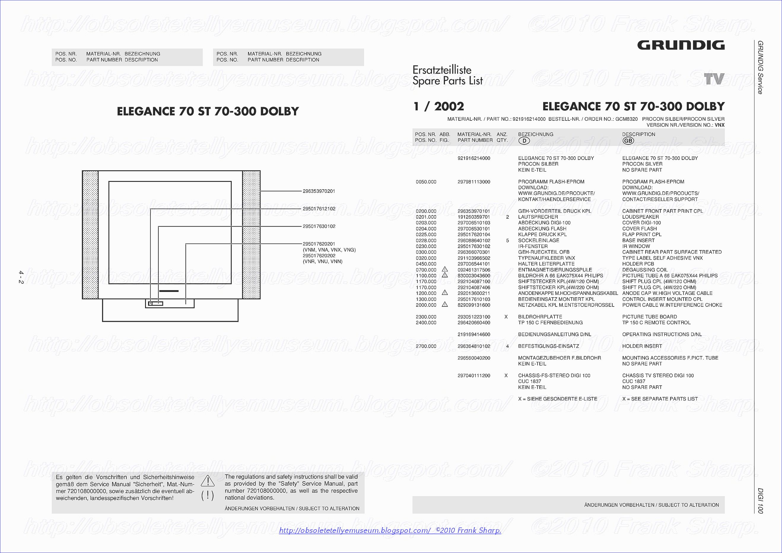
GRUNDIG ELEGANCE 63 ST63-300 DOLBY CHASSIS CUC1837 DIGI-100 FEATURE BAUSTEIN UNIT: 29504-203.2200
VPC 3215C Video Processor Family
The VPC 32x5 is a high-quality, single-chip video
front-end, which is targeted for 4:3 and 16:9, 50/60 and
100/120 Hz TV sets. It can be combined with other
members of the DIGIT3000 IC family (such as CIP
3250A, DDP 3300A, TPU 3040) and/or it can be used
with 3rd-party products.
The main features of the VPC 32x5 are
– all-digital video processing
– high-performance adaptive 4H comb filter Y/C separator
with adjustable vertical peaking
– multi-standard color decoder PAL/NTSC/SECAM
including all substandards
– 4 composite, 1 S-VHS input, 1 composite output
– integrated high-quality A/D converters and associated
clamp and AGC circuits
– multi-standard sync processing
– linear horizontal scaling (0.25 ... 4), as well as
non-linear horizontal scaling ‘panorama vision’
– PAL+ preprocessing (VPC 3215)
– line-locked clock, data and sync output (VPC 3215)
– display/deflection control (VPC 3205)
– submicron CMOS technology
– I2C-Bus Interface
– one 20.25 MHz crystal, few external components
– 68-pin PLCC package
1.1. System Architecture
Fig. 1–1 shows the block diagram of the video processor.
1.2. Video Processor Family
The VPC video processor family supports 15/32 kHz
systems and is available with different comb filter
options. The 50 Hz/single scan versions provide controlling
for the display and the vertical/east west deflection
of DDP 3300A. The 100 Hz/double scan versions
have a line-locked clock output interface and the
PAL+ preprocessing option. Table 1–1 gives an overview
of the VPC video processor family.
VPC Applications
Fig. 1–2 depicts several VPC applications. Since the
VPC functions as a video front-end, it must be complemented
with additional functionality to form a complete
TV set.
The DDP 33x0 contains the video back-end with video
postprocessing (contrast, peaking, DTI,...), H/V-deflection,
RGB insertion (SCART, Text, PIP,...) and tube
control (cutoff, white drive, beam current limiter). It
generates a beam scan velocity modulation output
from the digital YCrCb and RGB signals. Note that this
signal is not generated from the external analog RGB
inputs.
The CIP 3250A provides a high quality analog RGB
interface with character insertion capability. This allows
appropriate processing of external sources, such as
MPEG2 set-top boxes in transparent (4:2:2) quality.
Furthermore, it translates RGB/Fastblank signals to
the common digital video bus and makes those signals
available for 100 Hz upconversion or double scan processing.
In some European countries (Italy), this feature
is mandatory.
The IP indicates memory based image processing,
such as scan rate conversion, vertical processing
(Zoom), or PAL+ reconstruction.
Examples:
– Europe: 15 kHz/50 Hz → 32 kHz/100 Hz interlaced
– US: 15 kHz/60 Hz → 32 kHz/60 Hz non-interlaced
Note that the VPC supports memory based applications
through line-locked clocks, syncs, and data. CIP
may run either with the native DIGIT3000 clock but
also with a line-locked clock system.
Functional Description
2.1. Analog Front-End
This block provides the analog interfaces to all video
inputs and mainly carries out analog-to digital conversion
for the following digital video processing. A block
diagram is given in Fig. 2–1.
Most of the functional blocks in the front-end are digitally
controlled (clamping, AGC, and clock-DCO). The
control loops are closed by the Fast Processor (‘FP’)
embedded in the decoder.
2.1.1. Input Selector
Up to five analog inputs can be connected. Four inputs
are for input of composite video or S-VHS luma signal.
These inputs are clamped to the sync back porch and are
amplified by a variable gain amplifier. One input is for
connection of S-VHS carrier-chrominance signal. This
input is internally biased and has a fixed gain amplifier.
2.1.2. Clamping
The composite video input signals are AC coupled to
the IC. The clamping voltage is stored on the coupling
capacitors and is generated by digitally controlled current
sources. The clamping level is the back porch of
the video signal. S-VHS chroma is also AC coupled.
The input pin is internally biased to the center of the
ADC input range.
2.1.3. Automatic Gain Control
A digitally working automatic gain control adjusts the
magnitude of the selected baseband by +6/–4.5 dB in
64 logarithmic steps to the optimal range of the ADC.
The gain of the video input stage including the ADC is
213 steps/V with the AGC set to 0 dB.
2.1.4. Analog-to-Digital Converters
Two ADCs are provided to digitize the input signals.
Each converter runs with 20.25 MHz and has 8 bit resolution.
An integrated bandgap circuit generates the
required reference voltages for the converters. The
two ADCs are of a 2-stage subranging type.
2.1.5. Digitally Controlled Clock Oscillator
The clock generation is also a part of the analog front
end. The crystal oscillator is controlled digitally by the
control processor; the clock frequency can be adjusted
within ±150 ppm.
2.1.6. Analog Video Output
Th
e input signal of the Luma ADC is available at theanalog video output pin. The signal at this pin must be
buffered by a source follower. The output voltage is
2 V, thus the signal can be used to drive a 75 Ω line.
The magnitude is adjusted with an AGC in 8 steps
together with the main AGC.
Adaptive Comb Filter
The 4H adaptive comb filter is used for high-quality
luminance/chrominance separation for PAL or NTSC
composite video signals. The comb filter improves the
luminance resolution (bandwidth) and reduces interferences
like cross-luminance and cross-color. The adaptive
algorithm eliminates most of the mentioned errors
without introducing new artifacts or noise.
A block diagram of the comb filter is shown in Fig. 2–2.
The filter uses four line delays to process the information
of three video lines. To have a fixed phase relationship
of the color subcarrier in the three channels,
the system clock (20.25 MHz) is fractionally locked to
the color subcarrier. This allows the processing of all
color standards and substandards using a single crystal
frequency.
The CVBS signal in the three channels is filtered at the
subcarrier frequency by a set of bandpass/notch filters.
The output of the three channels is used by the
adaption logic to select the weighting that is used to
reconstruct the luminance/chrominance signal from
the 4 bandpass/notch filter signals. By using soft mixing
of the 4 signals switching artifacts of the adaption
algorithm are completely suppressed.
The comb filter uses the middle line as reference,
therefore, the comb filter delay is two lines. If the comb
filter is switched off, the delay lines are used to pass
the luma/chroma signals from the A/D converters to
the luma/chroma outputs. Thus, the processing delay
is always two lines.
In order to obtain the best-suited picture quality , the
user has the possibility to influence the behaviour of
the adaption algorithm going from moderate combing
to strong combing. Therfore, the following three parameters
may be adjusted:
– HDG ( horizontal difference gain )
– VDG ( vertical difference gain )
– DDR ( diagonal dot reducer )
HDG typically defines the comb strength on horizontal
edges. It determines the amount of the remaining
cross-luminance and the sharpness on edges respectively.
As HDG increases, the comb strength, e. g.
cross luminance reduction and sharpness, increases.
VDG typically determines the comb filter behaviour on
vertical edges. As VDG increases, the comb strength,
e. g. the amount of hanging dots, decreases.
After selecting the combfilter performance in horizontal
and vertical direction, the diagonal picture performance
may further be optimized by adjusting DDR. As
DDR increases, the dot crawl on diagonal colored
edges is reduced.
To enhance the vertical resolution of the the picture,
the VPC 32x5 provides a vertical peaking circuitry. The
filter gain is adjustable between 0 – +6 dB and a coring
filter suppresses small amplitudes to reduce noise artifacts.
In relation to the comb filter, this vertical peaking
widely contributes to an optimal two-dimensional resolution
homogeneity.
2.3. Color Decoder
In this block, the standard luma/chroma separation
and multi-standard color demodulation is carried out.
The color demodulation uses an asynchronous clock,
thus allowing a unified architecture for all color standards.
If the adaptive comb filter is used for luma chroma
separation, the color decoder uses the S-VHS mode
processing. The output of the color decoder is YCrCb
in a 4:2:2 format.
2.3.1. IF-Compensation
With off-air or mistuned reception, any attenuation at
higher frequencies or asymmetry around the color subcarrier
is compensated. Four different settings of the
IF-compensation are possible (see Fig. 2–3):
– flat (no compensation)
– 6 dB/octave
– 12 dB/octave
– 10 dB/MHz
The last setting gives a very large boost to high frequencies.
It is provided for SECAM signals that are
decoded using a SAW filter specified originally for the
PAL standard.
Frequency response of chroma IF-compensation
2.3.2. Demodulator
The entire signal (which might still contain luma) is
quadrature-mixed to the baseband. The mixing frequency
is equal to the subcarrier for PAL and NTSC,
thus achieving the chroma demodulation. For SECAM,
the mixing frequency is 4.286 MHz giving the quadrature
baseband components of the FM modulated
chroma. After the mixer, a lowpass filter selects the
chroma components; a downsampling stage converts
the color difference signals to a multiplexed half rate
data stream.
The subcarrier frequency in the demodulator is generated
by direct digital synthesis; therefore, substandards
such as PAL 3.58 or NTSC 4.43 can also be
demodulated.
2.3.3. Chrominance Filter
The demodulation is followed by a lowpass filter for the
color difference signals for PAL/NTSC. SECAM requires
a modified lowpass function with bell-filter characteristic.
At the output of the lowpass filter, all luma
information is eliminated.
The lowpass filters are calculated in time multiplex for
the two color signals. Three bandwidth settings (narrow,
normal, broad) are available for each standard
(see Fig. 2–5). For PAL/NTSC, a wide band chroma filter
can be selected. This filter is intended for high
bandwidth chroma signals, e.g. a nonstandard wide
bandwidth S-VHS signal.
2.3.4. Frequency Demodulator
The frequency demodulator for demodulating the SECAM
signal is implemented as a CORDIC-structure. It
calculates the phase and magnitude of the quadrature
components by coordinate rotation.
The phase output of the CORDIC processor is differentiated
to obtain the demodulated frequency. After
the deemphasis filter, the Dr and Db signals are scaled
to standard CrCb amplitudes and fed to the crossover-
switch.
2.3.5. Burst Detection
In the PAL/NTSC-system the burst is the reference for
the color signal. The phase and magnitude outputs of
the CORDIC are gated with the color key and used for
controlling the phase-lock-loop (APC) of the demodulator
and the automatic color control (ACC) in PAL/NTSC.
The ACC has a control range of +30 ... –6 dB.
For SECAM decoding, the frequency of the burst is
measured. Thus, the current chroma carrier frequency
can be identified and is used to control the SECAM
processing. The burst measurements also control the
color killer operation; they can be used for automatic
standard detection as well.
2.3.6. Color Killer Operation
The color killer uses the burst-phase/burst-frequency
measurement to identify a PAL/NTSC or SECAM color
signal. For PAL/NTSC, the color is switched off (killed)
as long as the color subcarrier PLL is not locked. For
SECAM, the killer is controlled by the toggle of the
burst frequency. The burst amplitude measurement is
used to switch-off the color if the burst amplitude is
below a programmable threshold. Thus, color will be
killed for very noisy signals. The color amplitude killer
has a programmable hysteresis.
2.3.7. PAL Compensation/1-H Comb Filter
The color decoder uses one fully integrated delay line.
Only active video is stored.
The delay line application depends on the color standard:
– NTSC: 1-H comb filter or color compensation
– PAL: color compensation
– SECAM: crossover-switch
In the NTSC compensated mode, Fig. 2–6 c), the color
signal is averaged for two adjacent lines. Thus,
cross-color distortion and chroma noise is reduced. In
the NTSC 1-H comb filter mode, Fig. 2–6 d), the delay
line is in the composite signal path, thus allowing
reduction of cross-color components, as well as
cross-luminance. The loss of vertical resolution in the
luminance channel is compensated by adding the vertical
detail signal with removed color information. If the
4H adaptive comb filter is used, the 1-H NTSC comb
filter has to be deselected.
2.4. Horizontal Scaler
The 4:2:2 YCrCb signal from the color decoder is processed
by the horizontal scaler. The scaler block
allows a linear or nonlinear horizontal scaling of the
input video signal in the range of 0.25 to 4. Nonlinear
scaling, also called “panorama vision”, provides a
geometrical distortion of the input picture. It is used to
fit a picture with 4:3 format on a 16:9 screen by stretching
the picture geometry at the borders. Also, the
inverse effect can be produced by the scaler. A summary
of scaler modes is given in Table 2–1.
The scaler contains a programmable decimation filter,
a 1-line FIFO memory, and a programmable interpolation
filter. The scaler input filter is also used for pixel
skew correction, see 2.3.9. The decimator/interpolator
structure allows optimal use of the FIFO memory. The
controlling of the scaler is done by the internal Fast
Processor.
2.5. Blackline Detector
In case of a letterbox format input video, e.g. Cinemascope,
PAL+ etc., black areas at the upper and lower
part of the picture are visible. It is suitable to remove or
reduce these areas by a vertical zoom and/or shift
operation.
The VPC 32xx supports this feature by a letterbox
detector. The circuitry detects black video lines by
measuring the signal amplitude during active video.
For every field the number of black lines at the upper
and lower part of the picture are measured, compared
to the previous measurement and the minima are
stored in the I2C-register BLKLIN. To adjust the picture
amplitude, the external controller reads this register,
calculates the vertical scaling coefficient and transfers
the new settings, e.g. vertical sawtooth parameters,
horizontal scaling coefficient etc., to the VPC.
Letterbox signals containing logos on the left or right
side of the black areas are processed as black lines,
while subtitles, inserted in the black areas, are processed
as non-black lines. Therefore the subtitles are
visible on the screen. To suppress the subtitles, the
vertical zoom coefficient is calculated by selecting the
larger number of black lines only. Dark video scenes
with a low contrast level compared to the letterbox
area are indicated by the BLKPIC bit.
2.6. Control and Data Output Signals
The VPC 32x
x supports two output modes: InDIGIT3000 mode, the output interfaces run at the main
system clock, in line-locked mode, the VPC generates
an asynchronous line-locked clock that is used for the
output interfaces.
2.6.1. Line-Locked Clock Generation
An on-chip rate multiplier will be used to synthesize
any desired output clock frequency of 13.5/16/18 MHz.
A double clock frequency output is available to support
100 Hz systems. The synthesizer is controlled by the
embedded RISC controller, which also controls all
front-end loops (clamp, AGC, PLL1, etc.). This allows
the generation of a line-locked output clock regardless
of the system clock (20.25 MHz) which is used for
comb filter operation and color decoding. The control
of scaling and output clock frequency is kept independent
to allow aspect ratio conversion combined with
sample rate conversion. The line-locked clock circuity
generates control signals, e.g. horizontal/vertical sync,
active video output, it is also the interface from the
internal (20.25 MHz) clock to the external line-locked
clock system.
If no line-locked clock is required, i.e. in the DIGIT3000
mode, the system runs at the 20.25 MHz main clock.
The horizontal timing reference in this mode is provided
by the front-sync signal. In this case, the
line-locked clock block and all interfaces run from the
20.25 MHz main clock. The synchronization signals
from the line-locked clock block are still available, but
for every line the internal counters are reset with the
main-sync signal. A double clock signal is not available
in DIGIT3000 mode.
Sync Signals
The front end will provide a number of sync/control signals
which are output with the output clock. The sync
signals are generated in the line-locked clock block.
– Href : horizontal sync
– AVO: active video out (programmable)
– HC: horizontal clamp (programmable)
– Vref : vertical sync
– INTLC: interlace
– HELPER: PAL+ helper lines
All horizontal signals are not qualified with field information,
i.e. the signals are present on all lines.
2.6.3. DIGIT3000 Output Format
The picture bus format between all DIGIT3000 ICs is
4:2:2 YCrCb with 20.25 MHz samples/s. Only active
video is transferred, synchronized by the system main
sync signal (MSY) which indicates the start of valid
data for each scan line and which initializes the color
multiplex. The video data is orthogonally sampled
YCrCb, the output format is given in Table 2–2. The
number of active samples per line is 1080 for all standards
(525 and 625).
The output can be switched to 4:1:1 mode with the output
format according to Table 2–3.
Via the MSY line, serial data is transferred which contains
information about the main picture such as current
line number, odd/even field etc.). It is generated
by the deflection circuitry and represents the orthogonal
timebase for the entire system.
2.6.4. Line-Locked 4:2:2 Output Format
In line-locked mode, the VPC 32xx will produce the
industry standard pixel stream for YCrCb data. The difference
to DIGIT3000 native mode is only the number
of active samples, which of course, depends on the
chosen scaling factor. Thus, Table 2–2 is valid for both
4:2:2 modes.
2.6.5. Line-Locked 4:1:1 Output Format
The orthogonal 4:1:1 output format is compatible to the
industry standard. The YCrCb samples are skew-corrected
and interpolated to an orthogonal sampling raster
(see Table 2–3).
note: C*x
Y (x = pixel number and y = bit number)
2.6.6. Output Code Levels
Output Code Levels correspond to ITU-R code levels:
Y = 16...240
Black Level = 16
CrCb = 128±112
An overview over the output code levels is given in
Table 2–4.
2.6.7. Output Signal Levels
All data and sync lines operate at TTL compliant levels.
With an optional external 3.3 V supply for the output
pins, reduced voltage swings can be obtained.
2.6.8. Test Pattern Generator
The YCrCb outputs can be switched to a test mode
where YCrCb data are generated digitally in the
VPC32xx. Test patterns include luma/chroma ramps,
flat field, and a pseudo color bar.
Video Sync Processing
To extract the sync information from thevideo signal, a linear phase lowpass filter eliminates all
noise and video contents above 1 MHz. The sync is
separated by a slicer; the sync phase is measured. A
variable window can be selected to improve the noise
immunity of the slicer. The phase comparator measures
the falling edge of sync, as well as the integrated
sync pulse.
The sync phase error is filtered by a phase-locked loop
that is computed by the FP. All timing in the front-end is
derived from a counter that is part of this PLL, and it
thus counts synchronously to the video signal.
A separate hardware block measures the signal back
porch and also allows gathering the maximum/minimum
of the video signal. This information is processed
by the FP and used for gain control and clamping.
For vertical sync separation, the sliced video signal is
integrated. The FP uses the integrator value to derive
vertical sync and field information.
The information extracted by the video sync processing
is multiplexed onto the hardware front sync signal
(FSY) and is distributed to the rest of the video processing
system. The format of the front sync signal is
given in Fig. 2–13.
The data for the vertical deflection, the sawtooth, and
the East-West correction signal is calculated by the
VPC 32xx. The data is buffered in a FIFO and transferred
to the back-end IC DDP 3300A by a single wire
interface.
Frequency and phase characteristics of the analog
video signal are derived from PLL1. The results are fed
to the scaler unit for data interpolation and orthogonalization
and to the clock synthesizer for line-locked
clock generation. Horizontal and vertical syncs are
latched with the line-locked clock.
Pin Descriptions
(pin numbers for PLCC68 package)
Pin 1 – Ground, Analog Front-End GNDF
Pin 2 – Ground, Analog Front-End GNDF
Pin 3 – CCU 5 MHz Clock Output CLK5 (Fig. 4–11)
This pin provides a clock frequency for the TV microcontroller,
e.g. a CCU 3000 controller. It is also used
by the DDP 3300A display controller as a standby
clock.
Pin 4 – Standby Supply Voltage VSTDBY
In standby mode, only the clock oscillator is active,
GNDF should be ground reference. Please activate
RESQ before powering-up other supplies
Pins 6 and 5 – XTAL1 Crystal Input and XTAL2 Crystal
Output (Fig. 4–8)
These pins are connected to an 20.25 MHz crystal
oscillator which is digitally tuned by integrated shunt
capacitances. The CLK20 and CLK5 clock signals are
derived from this oscillator. An external clock can be
fed into XTAL1. In this case, clock frequency adjustment
must be switched off.
Pin 7 – Ground, Analog Front-End GNDF
Pin 9 – Ground, Output Pad Circuitry GNDP
Pin 10 – Interlace Output, INTLC (Fig. 4–4)
This pin supplies the interlace information, 0 indicates
first field, 1 indicates second field.
Pin 12 – Vertical Sync Pulse, VS (Fig. 4–4)
This pin supplies the vertical sync signal.
Pin 13 – Front Sync Pulse, FSY (Fig. 4–4)
This pin supplies the front sync information.
Pin 14 – Main Sync/Horizontal Sync Pulse MSY/HS
(Fig. 4–4)
This pin supplies the horizontal sync pulse information
in line-locked mode. In DIGIT3000 mode, this pin is the
main sync input.
Pin 15 – Helper Line Output, Helper (Fig. 4–4)
This signal indicates a helper line in PAL+ mode.
Pin 16 – Horizontal Clamp Pulse, HC (Fig. 4–4)
This signal can be used to clamp an external video signal,
that is synchronous to the input signal. The timing
is programmable.
Pin 17 – Active Video Output, AVO (Fig. 4–4)
This pin indicates the active video output data. The
signal is clocked with the LLC1 clock.
Pin 18 – Double Output Clock, LLC2 (Fig. 4–6)
Pin 19 – Output Clock, LLC1 (Fig. 4–6)
This is the clock reference for the luma, chroma, and
status outputs.
Pin 26 – Ground, Output Pad Circuitry GNDP
Pins 20 to 25,28,29 – Luma Outputs Y0 – Y7 (Fig. 4–4)
These output pins carry the digital luminance data. The
data are clocked with the LLC1 clock.
Pin 30 – Main Clock Output CLK20 (Fig. 4–5)
This is the 20.25 MHz main clock output.
Pin 31 – Supply Voltage, Digital Circuitry VSUPD
Pin 34 – Ground, Digital Circuitry GNDD
Pin 35 – Ground, Output Pad Circuitry GNDP
Pin 36 – Supply Voltage, Output Pad Supply VSUPP
Pins 38 to 43,46,47 – Chroma Outputs C0–C7 (Fig. 4–4)
These outputs carry the digital CrCb chrominance data.
The data are clocked with the LL1 clock. The data are
sampled at half the clock rate and multiplexed. The
CrCb multiplex is reset for each TV line.
Pins 48 to 50 – Picture Bus Priority PR0–PR2 (Fig. 4–6)
The Picture Bus Priority lines carry the digital priority
selection signals. The priority interface allows digital
switching of up to 8 sources to the back-end processor.
Switching for different sources is prioritized and can be
on a per pixel basis.
Pin 51 – Ground, Output Pad Circuitry GNDP
Pin 52 – VGAV-Input. (Fig. 4–3)
This pin is connected to the vertical sync signal of a VGA
signal.
Pin 53 – Front-End/Back-End Data FPDAT (Fig. 4–6)
This pin interfaces to the DDP 3300A back-end processor.
The information for the deflection drives and
for the white drive control, i.e. the beam current limiter,
is transmitted by this pin.
Pin 54 – Reset Input RESQ (Fig. 4–3)
A low level on this pin resets the VPC 32xx.
Pin 55 – I2C Bus Data SDA (Fig. 4–13)
This pin connects to the I2C bus data line.
Pin 56 – I2C Bus Clock SCL (Fig. 4–3)
This pin connects to the I2C bus clock line.
Pin 57 – Test Input TEST (Fig. 4–3)
This pin enables factory test modes. For normal operation,
it must be connected to ground.
Pin 59 – Ground, Analog Front-End GNDF
Pins 62,61,60,58 – Video Input 1–4 (Fig. 4–12)
These are the analog video inputs. A CVBS or S-VHS
luma signal is converted using the luma (Video 1) AD
converter. The VIN1 input can also be switched to the
chroma (Video 2) ADC. The input signal must be
AC-coupled.
Pin 63 – Chroma Input CIN (Fig. 4–10)
This pin is connected to the S-VHS chroma signal. A
resistive divider is used to bias the input signal to the
middle of the converter input range. CIN can only be
connected to the chroma (Video 2) A/D converter. The
signal must be AC-coupled.
Pin 64 – Analog Video Output, VOUT (Fig. 4–7)
The analog video signal that is selected for the main
(luma, CVBS) ADC is output at this pin. An emitter follower
is required at this pin.
Pin 65 – Ground, Analog Shield Front-End GNDF
Pin 66 – Supply Voltage, Analog Front-End VSUPF
(Fig. 4–9)
Pin 67 – Signal GND for Analog Input ISGND (Fig. 4–
11) This is the high quality ground reference for the
video input signals.
Pin 68 – Reference Voltage Top VRT (Fig. 4–9)
Via this pin, the reference voltage for the A/D converters
is decoupled. The pin is connected with 10 µF/47 nF to
the Signal Ground Pin
SDA 9401 SCARABAEUS Scan Rate Converter using Embedded DRAM Technology Units
1 General descriptionThe SDA 9401 is a new component of the Micronas MEGAVISION® IC set in a 0.35 µm embedded
DRAM technology (field memory embedded). The SDA 9401 is pin compatible to the SDA 9400
(frame memory embedded). The SDA 9401 comprises all main functionalities of a digital featurebox
in one monolithic IC.
The SDA 9401 does a simple 100/120 Hz interlaced (50/60 Hz progressive) scan rate conversion.
The scan rate converted picture can be vertically expanded. The SDA 9401 has a freerunning
mode, therefore features like multiple picture display (e.g. tuner scan) are possible.
The noise reduction is field based. Furthermore separate motion detectors for luminance and
chrominance have been implemented. For automatic controlling of the noise reduction parameters a
noise measurement algorithm is included, which measures the noise level in the picture or in the
blanking period. In addition a spatial noise reduction is implemented, which reduces the noise even
in the case of motion. The input signal can be compressed horizontally and vertically with a certain
number of factors. Therefore split screen modes are supported too.
Beside these additional functions like coloured background, windowing and flashing are
implemented.
2 Features
• Two input data formats
- 4:2:2 luminance and chrominance parallel (2 x 8 wires)
- ITU-R 656 data format (8 wires)
• Two different representations of input chrominance data
- 2‘s complement code
- Positive dual code
• Flexible input sync controller
• Flexible compression of the input signal
- Digital vertical compression of the input signal (1.0, 1.25, 1.5, 1.75, 2.0, 3.0, 4.0)
- Digital horizontal compression of the input signal (1.0, 2.0, 4.0)
• Noise reduction
- Motion adaptive spatial and temporal noise reduction (3D-NR)
- Temporal noise reduction for luminance field based
- Temporal noise reduction for chrominance field based
- Separate motion detectors for luminance and chrominance
- Flexible programming of the temporal noise reduction parameters
- Automatic measurement of the noise level (5 bit value, readable by I²C bus)
• TV mode detection by counting line numbers (PAL, NTSC, readable by I²C bus)
• Embedded memory
- 3.2 Mbit embedded DRAM core for field memories
- 128 kbit embedded DRAM core for line memories
• Flexible clock and synchronization concept
- Decoupling of the input and output clock system possible
• Scan rate conversion
- Simple 100/120 Hz interlaced scan conversion (e.g. AABB, AA*B*B)
- Simple progressive scan conversion (e.g. AA*)
• Flexible digital vertical expansion of the output signal (1.0, ... [1/32] ... , 2.0)
• Flexible output sync controller
- Flexible positioning of the output signal
- Flexible programming of the output sync raster
• Signal manipulations
- Insertion of coloured background
- Vertical and/or horizontal windowing with four different speed factors
- Flash generation
- Still field
- Support of split screen applications
- Multiple picture display - Tuner scan (4 and 16 times for 4:3, 12 times for 16:9 tubes)
- Support of multi picture display with PIP or front-end processor with integrated scaler
(e.g. 9 times display of PIP pictures, picture tracking, random pictures,
still-in-moving picture, moving-in-still picture)
• I²C-bus control (400 kHz)
• P-MQFP-64 package
• 3.3 V ± 5% supply voltage.
The SDA 9401 contains the blocks, which will be briefly described below:
ISC - Flexible input sync controller
IFC - Input format conversion
LDR - Low data rate processing (noise reduction and measurement, vertical compression,
horizontal compression)
MC - Memory controller
OSC - Flexible output sync controller
OFC - Output format conversion
HDR - High data rate processing (scan rate conversion, vertical expansion)
I²C - I²C bus interface
PLL1/2 - PLL for frequency doubling
LM - Line memory core
ED - eDRAM core
DDP 3310B Display and Deflection Processor
Display and Deflection Processor1. Introduction
The DDP 3310B is a single-chip digital Display and
Deflection Processor designed for high-quality backend
applications in 100/120-Hz TV sets with 4:3- or
16:9 picture tubes. The IC can be combined with members
of the DIGIT 3000 IC family (VPC 32xx,
TPU 3040), or it can be used with third-party products.
The IC contains the entire digital video component and
deflection processing and all analog interface components.
1.1. Main Features
Video processing
– linear horizontal scaling (0.25 … 4)
– non-linear horizontal scaling “panoramavision”
– dynamic peaking
– soft limiter (gamma correction)
– color transient improvement
– programmable RGB matrix
– picture frame generator
– two analog RGB/Fast-Blank inputs
Deflection processing
– scan velocity modulation output
– high-performance H/V deflection
– EHT compensation for vertical / East/West
– soft start/stop of H-Drive
– vertical angle and bow
– differential vertical output
– vertical zoom via deflection
– horizontal and vertical protection circuit
– adjustable horizontal frequency for VGA/SVGA display
Miscellaneous
– selectable 4:1:1/4:2:2 YCrCb input
– selectable 27/32-MHz line-locked clock input
– crystal oscillator for horizontal protection
– automatic picture tube adjustment (cutoff, whitedrive)
– single 5-V power supply
– hardware for simple 50/60-Hz to 100/120-Hz conversion
(display frequency doubling)
– two I2C-controlled PWM outputs
– beam current limiter
1.2. System ArchitectureThe DDP 3310B is a mixed-signal IC containing the
entire digital video component processing such as
chroma transient improvement (CTI), adaptive luma
peaking, and a non-linear ‘Panorama’ aspect ratio conversion.
All deflection related signals can be adapted
to different scan rates. The analog section contains all
analog interface components and an ADC, to compensate
long term changes of the picture tube parameters
and extreme high-tension effects. Fig. 1–1 shows the
block diagram of the single-chip Display and Deflection
Processor.
1.3. System Application
Fig. 1–2 depicts several DDP applications. Since the
DDP functions as a video back-end, it must be complemented
with additional functionality to form a complete
TV set.
The VPC 32xx family processes all worldwide analog
video signals (including the European PALplus) and
allows non-linear Panorama aspect ratio conversion.
Thus, 4:3 and 16:9 systems can easily be configured
by software. The aspect ratio scaling is also used as a
sample rate converter to provide a line-locked digital
component output bus (YCrCb) compliant to ITU-R-601.
All video processing and line-locked clock/data generation
is derived from a single 20.25-MHz crystal. An
optional adaptive 2H/4H comb filter (VPC 32xx) performs
Y/C separation for PAL and NTSC and all of their
substandards.
The VPC 32xxD and the CIP 3250A provide a highquality
analog RGB interface with character insertion
capability. This allows appropriate processing of external
sources such as MPEG 2 set-top boxes in transparent
(4:2:2) quality. Furthermore, it translates RGB/
Fast-Blank signals to the common digital video bus
and makes those signals available for 100-Hz processing.
In some European countries (Italy), this feature is
mandatory.
The IP indicates memory-based image processing,
such as scan rate conversion, vertical processing
(Zoom), or PAL+ reconstruction.
Examples:
– Europe: 15 kHz/ 50 Hz → 32 kHz/100 Hz interlaced
– US: 15 kHz/60 Hz → 31 kHz/120 Hz non-interlaced
Note: The DDP 3310B and the VPC 32xx families
support memory-based applications through linelocked
clocks, syncs, and data. The CIP 3250A may
run either with the native DIGIT3000 clock but also
with a line-locked clock system.
2. Functional Description
2.1. Display Part
The display part converts the digital YCrCb to analog
RGB (see Fig. 2–7) and provides contrast and saturation
adjustment. In case of YCrCb 4:1:1 an interpolation
filter is used, which converts the digital input signal
to YCrCb 4:2:2 standard. The 4:2:2 YCrCb signal is
processed by the horizontal scaler. In the luminance
processing path, a variety of features, such as
dynamic peaking and soft limiting, are provided. In the
chrominance path, the CrCb signals are converted to
4:4:4 format and filtered by a color transient improvement
circuit. The YCrCb signal is converted by a programmable
matrix to RGB color space.
2.1.1. Input Interface
The data inputs Y0…Y7 and C0…C7 are clocked with
the external clock LLC2. The clock frequency is selectable
for 27 or 32 MHz. A clock generator converts the
different external line-locked clock rates to a common
internal sample rate of appr. 40.5 MHz in order to provide
a fix bandwidth for all digital filters. The horizontal
scaler is used for conversion of scan rate and non-linear
aspect ratio. The horizontal sync puls at the HS pin
should be an active video signal, which is not vertically
blanked.
The input interface signals are
– external clock (LLC2)
– luma / chroma inputs (Y0…Y7 / C0…C7)
– horizontal sync (HS) / vertical sync (VS, VS2)
2.1.2. Horizontal Scaler
The scaler block allows linear or non-linear horizontal
scaling of the digital input video signal in the range of
0.25 to 4. Non-linear scaling, also called “panorama
vision”, provides a geometrical distortion of the input
picture. It is used to fit a picture with 4:3 format on a
16:9 screen by stretching the picture geometry at the
borders. The inverse effect can be produced by the
scaler, also. The scaler consists of a programmable
decimation and interpolation filter and a 1/2H FIFO
memory.
2.1.4. Dynamic Peaking
Especially with decoded composite signals and notch
filter luminance separation as input signals, it is necessary
to improve the luminance frequency characteristics.
With transparent high-bandwidth signals, it is
sometimes desirable to soften the image.
In the DDP 3310B, the luma frequency response is
improved by “dynamic” peaking. It adapts to the amplitude
and the frequency of the input signal. Small AC
amplitudes are sharpened while large AC amplitudes
remain nearly unmodified.
The dynamic range can be adjusted from −14 to
+14 dB for small high-frequency signals. There is separate
adjustment for signal overshoot and for signal
undershoot. For large signals, the dynamic range is
limited by a non-linear function that does not create
any visible alias components. The peaking can be
switched over to “softening” by inverting the peaking
term by software.
The center frequency of the peaking filter is selectable
from 2.5 MHz to 3.2 MHz. For S-VHS and for notch filter
color decoding, the total system frequency
responses for both PAL and NTSC are shown in Fig.
2–1 and Fig. 2–2. (All frequencies refer to a 50/60-Hz
video signal).
2.1.5. Soft Limiter
The dynamic range of the processed luma signal must
be limited to prevent the CRT from overload. An appropriate
headroom for contrast, peaking, and brightness
can be adjusted by the TV manufacturer according to
the CRT characteristics. All signals above this limit will
be “soft”-clipped. A characteristic diagram of the soft
limiter is shown in Fig. 2–3. The total limiter consists of
three parts:
Part A includes adjustable tilt point and gain. The gain
before the tilt value is 1. Above the tilt value, a part
(0…15/16) of the input signal is subtracted from the
input signal itself. Therefore, the gain is adjustable
from 16/16 to 1/16, when the slope value varies from 0
to 15. The tilt value can be adjusted from 0 to 511.
Part B has the same characteristics as part A. The
subtracting part is also relative to the input signal, so
the total differential gain will become negative if the
sum of slope A and slope B is greater than 16 and the
input signal is above the both tilt values (see characteristics).
Finally, the output signal of the soft limiter will be
clipped by a hard limiter adjustable from 256 to 511.
2.1.6. Chroma Input
The chroma input signal can either be YCrCb in 4:1:1
or in 4:2:2 format. For the digital signal processing, the
time-multiplexed chroma samples will be demultiplexed
and synchronized with the signal at the HS pin.
The input formatter accepts either two’s complement
or binary offset code. Also, the delay can be adjusted
within a range of ±2 input clocks relative to the luma
signal; this doesn’t affect the chroma multiplex.
2.1.7. Chroma Interpolation
In case of YCrCb 4:1:1 input format, an interpolation filter
is used which converts the digital input signal to
4:2:2 format. This filter runs with the incoming pixel
clock frequency.
The signal is passed to the scaler in YCrCb 4:2:2 format
in order to convert the incoming pixel clock frequency
(27/32 MHz) to the internal frequency (40.5/
40 MHz). A linear phase interpolator is used to convert
the chroma sampling rate from 4:2:2 to 4:4:4.
The frequency response of the interpolator is shown in
Fig. 2–4. All further processing is carried out at the full
sampling rate.
2.1.8. Chroma Transient Improvement
The intention of this block is to enhance the chroma
resolution. A correction signal is calculated by differentiation
of the color difference signals. The differentiation
can be selected according to the signal bandwidth,
e.g. for PAL/NTSC/SECAM or digital component signals,
respectively. The amplitude of the correction signal
is adjustable. Small noise amplitudes in the correction
signal are suppressed by an adjustable coring
circuit. To eliminate “wrong colors”, which are caused
by over and undershoots at the chroma transition, the
sharpened chroma signals are limited to a proper
value automatically.
2.1.9. Inverse Matrix and Digital RGB Processing
Six multipliers in parallel perform the matrix multiplication
to transform the Cr and Cb signals to R−Y, B−Y,
and G−Y. The initialization values for the matrix are
computed from the standard ITU-R (CCIR) matrix:
2.1.10. Picture Frame Generator
When the picture does not fill the total screen (height
or width too small) it is surrounded with black areas.
These areas (and more) can be colored with the picture
frame generator. Another possibility is the insertion
of a vertical and a horizontal stripe into the picture.
This is done by switching over the RGB signal from the
matrix to the signal from the frame color register.
The width of each area (left, right, upper, lower) can be
adjusted separately. The generator starts on the right,
respectively lower side of the screen and stops on the
left, respectively upper side of the screen. This means,
it runs during horizontal, respectively vertical flyback.
The color of the complete border can be stored in
a programmable frame color register. The format is
3×4 bit RGB. The contrast can be adjusted separately.
If the start value for the generator is larger than the
stop value, the picture frame is inserted at the borders.
If the start value is smaller than the stop value a vertical
or horizontal stripe is inserted.
2.1.11. Scan Velocity Modulation
Picture tubes equipped with an appropriate yoke can
use the Scan Velocity Modulation signal to vary the
speed of the electron gun during the entire video scan
line depending on its content. Transitions from dark to
bright will first speed up and then slow down the scan;
vice-versa for the opposite transition (see Fig. 2–6).
The digital RGB input signal for the SVM is converted
to Y in a simple matrix. Then the Y signal is differentiated
by a filter of the transfer function 1−Z−N, where N
is programmable from 1 to 6. With a coring some noise
can be suppressed. This is followed by a gain adjustment
and an adjustable limiter. The analog output signal
is generated by an 8-bit D/A converter. The signal
delay can be adjusted by ±3.5 clocks in half-clock
steps in respect to the analog RGB output signals.
This is useful to adjust the different group delays of
analog RGB amplifiers to the one for the SVM yoke
current.
2.2. Analog Back-End
The digital RGB signals are converted to analog RGB
using three video digital to analog converters (DAC)
with 10-bit resolution. The analog RGB-outputs are
current outputs with current-sink characteristics. The
maximum current drawn by the output stage is
obtained with peak white RGB.
Each RGB signal has two additional DAC’s with 9-bit
resolution to adjust analog brightness (40 % of the full
RGB range) and cutoff / black level (60 % of the full
RGB range). An additional fixed current is applied for
the blanking level.
In order to define accurate color on different CRT displays,
you must exactly adjust what color the CRT
phosphorous produces to display the color on screen.
To have the same colors for the life of the display, a
build-in automatic tube control loop checks and adjusts
the black level on every field and white point every third
field.
The back-end allows insertion of two external analog
RGB signals. The RGB signals are key-clamped and
inserted into the main RGB by the Fast-Blank switch.
The external RGB signals can be adjusted independently
as regarding DC-level (brightness) and magnitude
(contrast). An external Half-Contrast signal can
be used to reduce the output current of the internal
RGB outputs to 50 %.
The controlling of the white-drive/analog brightness
and also the external contrast and brightness adjustments
is done via the internal processor.
2.2.1. Analog RGB Insertion
The DDP 3310B allows insertion of two external analog
RGB signals. Each RGB signal is key-clamped and
inserted into the main RGB by the Fast-Blank switch.
The selected external RGB input can be overlaid or
underlaid to the digital picture. The external RGB signals
can be adjusted independently as regards DC
level (brightness) and magnitude (contrast).
It depends on the Fast-Blank input signals and the programming
of a number of I2C-register settings which
analog RGB input is selected. Both Fast-Blank inputs
must be either active-Low or active-High.
All signals for analog RGB insertion (RIN1/2, GIN1/2,
BIN1/2, FBLIN1/2, HCS) must be synchronized to the
horizontal flyback, otherwise a horizontal jitter will be
visible. The DDP 3310B has no means for timing correction
of the analog RGB input signals.
2.2.2. Half-Contrast Control
Insertion of transparent text pages or OSD onto the
video picture is often difficult to read, especially if the
video contrast is high. The DDP 3310B allows contrast
reduction of the video background by means of a Half-
Contrast input (HCS pin). This input can be supplied
with a fast switching signal (similar to the Fast-Blank
input), typically defining a rectangular box in which the
video picture is displayed with reduced contrast. The
analog RGB inputs are still displayed with full contrast.
2.2.3. Fast-Blank Monitor
The presence of external analog RGB sources can be
detected by means of a Fast-Blank monitor. The status
of the selected Fast-Blank input can be monitored via
an I2C register. There is a 2-bit information, giving
static and dynamic indication of a Fast-Blank signal.
The static bit is directly reading the Fast-Blank input
line, whereas the dynamic bit is reading the status of a
flip flop triggered by the negative edge of the Fast-
Blank signal.
With this monitor logic it is possible to detect if there is
an external RGB source active and if it is a full-screen
insertion or only a box. The monitor logic is connected
directly to the FBLIN1 or FBLIN2 pin. Selection is done
via I2C register.
Fig. 2–9: Fast-Blank selection logic
2.2.4. CRT Measurement and Control
The display processor is equipped with an 8/12-bit
PDM-ADC for all picture tube measuring purposes.
This MADC is connected to the SENSE input pin, the
input range is 0 to 1.6V.
Cutoff and white-drive current measurement are carried
out with 8-bit resolution during the vertical blanking
interval. The current range for cutoff measurement
is set by connecting the resistor R1 to the SENSE
input. Due to the fact of a 1:10 relation between cutoff
and white-drive current, the range select 2 output
(RSW2) becomes active for the white-drive measurement
and connects R3 in parallel to R1, thus determining
the correct current range. During the active picture,
the MADC is used for the average beam current limiter
with a 12-bit resolution. Again, a different measurement
range is selected with active range select 1&2
outputs (RSW1&RSW2) connecting R2 in parallel to
R3 and R1. See Fig. 2–10 and Fig. 2–11 for the corresponding
timing. These measurements are typically
done at the summation point of the picture tube cathode
currents.
Another method uses two different current measurements.
The range switch 1 pin (RSW1) can be used as
a second Sense input, selectable by software. In this
case, the cutoff and white-drive currents are measured
as before at the SENSE input. The active picture measurement
can be done with the second Sense input
(RSW1). The signal may come (via a proper interface)
from the low end of the EHT coil (CRT anode current).
In this case, the resistor R2 in Fig. 2–10 has to be
removed.
The picture tube measurement returns results on
every field for:
– cutoff R
– cutoff G
– cutoff B
– white-drive R or G or B (sequentially)
Thus, a cutoff control cycle for RGB requires one field
only while a complete white-drive control cycle
requires three fields. During cutoff and white-drive
measurement the average beam current limiter function
(see Section 2.2.5.) is switched off. The amplitude
of the cutoff and white-drive measurement lines can be
programmed separately with IBRM and WDRM (see
Fig. 2–11). The start line for the tube measurement
(cutoff red) can be programmed via I2C-bus (TML).
The built-in control loop for cutoff and white-drive can
operate in three different modes selected by
CUT(WDR)_GAIN and CUT(WDR)_DIS.
– The user control mode is selected by setting
CUT(WDR)_GAIN = 0. In this mode the registers
CUT(WDR)_R/G/B are used as direct control values
for cutoff and drive using the whole 9-bit range. If
the measurement lines are enabled
(CUT(WDR)_DIS = 0) the user can read the measured
cutoff & white drive values in the CUTOFF(
WDRIVE)_R/G/B registers. An external software
can now control the settings of the
CUT(WDR)_R/G/B registers.
– The automatic mode is selected by setting
CUT(WDR)_GAIN > 0 and CUT(WDR)_DIS = 0. In
this mode, the registers CUT(WDR)_R/G/B are
used as reference for the measured values (CUTOFF(
WDRIVE)_R/G/B). Due to the 8-bit resolution
of the ADC, only 8 LSB can be used as reference
values. The calculated error is used with a small
hysteresis (1,5 %) to adjust cutoff and drive. The
higher the loop gain (CUT(WDR)_GAIN), the
smaller the time constant for the adjustment.
– If the automatic mode was once enabled
(CUT(WDR)_GAIN > 0), the control loop can be
stopped by setting CUT(WDR)_DIS = 1. In this
mode, the calculated cutoff and drive values will no
longer be modified and the measurement lines are
suppressed. Changes of the reference values
(CUT(WDR)_R/G/B) have no effect.
If one of the calculated red, green, or blue white-drive
values exceeds its maximal possible value (WDR_R/
G/B>511), the white balance gets misadjusted. An
automatic drive saturation avoidance prevents from
this effect (WDR_SAT = 1) from occurring. If one drive
value exceeds the maximum allowed threshold
(MAX_WDR), the amplitude of the white-drive measurement
line will be increased and decreased if one
of them goes below the fixed threshold 475.
2.2.5. Average Beam Current Limiter
The average beam current limiter (BCL) works on both
the digital YUV input and the inserted analog RGB signals
by using either the sense input or the RSW1 input
for the beam current measurement. The BCL uses a
different filter to average the beam current during the
active picture resulting in a 12-bit resolution. The filter
bandwidth is approximately 4 kHz.
The beam current limiter allows the setting of a threshold
current, a gain and an additional time constant. If
the beam current is above the threshold, the excess
current is low-pass filtered with the according gain and
time constant. The result is used to attenuate the RGB
outputs by adjusting the white-drive multipliers for the
internal (digital) RGB signals and the analog contrast
multipliers for the analog RGB inputs, respectively. The
lower limit of the attenuator is programmable, thus a
minimum contrast can always be set. If the minimum
contrast is reached, the brightness will be decreased
down to a programmable minimum as well. Typical
characteristics of the BCL for different loop gains are
shown in Fig. 2–12; for this example the tube has been
assumed to have square-law characteristics.
2.3. Synchronization and Deflection
2.3.1. Deflection Processing
The deflection processing generates the signals for the
horizontal and vertical drive (see Fig. 2–13). This block
contains two numeric phase-locked loops and a security
unit:
– PLL2 generates the horizontal and vertical timing,
e.g. blanking, clamping, and sync signals. Phase
and frequency are synchronized by the incoming
sync signals.
– PLL3 adjusts the phase of the horizontal drive pulse
and compensates for the delay of the horizontal output
stage.
– The security unit observes the H-Drive output signal.
With an external 5-MHz reference clock, this
unit controls the H-Drive “off time” and period. In
case of an incorrect H-Drive signal the security unit
generates a free-running H-Drive signal divided
down from the 5-MHz reference clock.
The DDP 3310B is able to synchronize various horizontal
frequencies, even VGA frequencies. Allowed
horizontal frequencies are listed in Table 2–5. The horizontal
drive uses a high-voltage (8 V) open-drain output
transistor.
2.3.2. Security Unit for H-Drive
The security unit observes the H-Drive output signal
with an external 5-MHz reference clock. For different
horizontal frequencies the security unit uses different
ranges to control the H-Drive signal. Selecting a specific
horizontal frequency via I2C-register HFREQ
automatically switches to the corresponding security
range. The control ranges are listed in Table 2–5.
The window of the control range has to fit into a main
control window which is selectable with the FREQSEL
input pin. With a Low signal at this pin, the main control
range is 28.8…34.4 µs and with a High signal, the
main control range is 25.6…29.2 µs. This is to prevent
malfunctions if the horizontal deflection stage is prepared
for VGA frequencies.
The Horizontal Drive Output can be forced to the High
level during Flyback. This means, the falling edge of
the drive pulse occurs at the earliest to the end of the
flyback pulse. This function can be enabled via the I2C
bus (EFLB).
2.3.3. Soft Start/Stop of Horizontal Drive
In order to increase the energy supply of the horizontal
deflection stage smoothly, a soft start decreases the
drive frequency from 55 kHz to 31.25 kHz within
85 ms. The High time tH is always 14.4 µs. This
means, the duty factor decreases from 79.2 % to 45 %
(see Fig. 2–14).
The soft stop is needed, when the protection circuitry
wants to turn off the H-Drive. It has the inverse behavior
of the soft start and ends with a High level at the
HOUT Pin.
2.3.4. Horizontal Phase Adjustment
This section describes a simple way to get a correct
horizontal frame position and clamp window for analog
RGB insertion.
1. For a correct scaler function in panorama/waterglass
mode, the digital input data should be centered
to the active video input signal.
2. The clamping pulse for analog RGB insertion can be
adjusted to the pedestal of the input signal with
POFS2.
3. The horizontal raster position of the analog inserted
RGB1/2 signal can be set to the desired frame position
with POFS3.
4. The horizontal position of the digital RGB signal can
be shifted to the left and right with NEWLIN. Following
values allowed in respect to POFS2:
− 90 < (POFS2+NEWLIN) − (Clk×SFIF) < 580
− Clk = 3 @ LLC2 = 27 MHz
− Clk = 2.5 @ LLC2 = 32 MHz
5. Now the positioning of horizontal blanking and the
picture frame generator can be done.
2.3.5. Vertical Synchronization
The number of lines per field can be adjusted by software
(LPFD). This number is used to calculate the vertical
raster. The DDP synchronizes only to a vertical
sync within a programmable detection window (LPFD
± VSYNCWIN). If there is no vsync, the DDP runs with
maximum allowed lines and if the vertical frequency is
to high, it runs with minimum allowed lines. The
smaller the detection window, the slower the DDP gets
synchronized to the incoming vertical sync. In case of
an interlaced input signal, it is possible to display both
fields at the same raster position by setting R_MODE
to 1 or 2.
An automatic field length adaptation can be selected
(VA_MODE). In this case, the vertical raster will be calculated
according to the counted number of lines per
field instead from LPFD. This is useful for video
recorder search mode when the number of lines per
field does not comply with the standard, or if you want
to use a common value of LPFD for PAL and NTSC
(e.g.: LPFD = 290; VSYNCWIN = 54).
2.3.6. Vertical and East/West Deflection
The calculations of the Vertical deflection and East/
West correction waveforms are done in the internal
processor. They are described as polynomials in x,
where x varies from −0.5×zoom to +0.5×zoom for one
field. For zoom>1 the range is limited between −0.5
and +0.5.
The vertical deflection waveform is calculated as follows
(without EHT compensation):
– VPOS defines the vertical raster position
– AMPL is the vertical raster amplitude (zoom≥1)
– LIN is the linearity coefficient
– SCORR is the coefficient for S-correction
The vertical sawtooth signal will be generated from a
differential current D/A converter and can drive a DC
coupled power stage. In order to get a faster vertical
retrace timing, the output current of the vertical D/Aconverter
can be increased during the retrace for a
programmable number of lines (FLYBL). The range
between the end of the flyback and the beginning of
the raster is also programmable (HOLDL).
The East/West deflection waveform, generated from a
single-ended D/A converter, is given with the equation:
– WIDTH is a DC value for the picture width
– TCORR is the trapezoidal correction
– CUSH is the pincushion correction
– CRNU is the upper corner correction
– CRNL is the lower corner correction
Fig. 2–15: Vertical and East/West deflection waveforms
V vpos ampl x( lin x2 scorr x3 ) ⋅ + ⋅ + ⋅ + =
E W ⁄ width tcorr x cush x2 corner x4
2.3.7. Vertical Zoom
With vertical zoom, the DDP 3310B is able to display
different aspect ratios of the source signal on tubes
with 4:3 or 16:9 aspect ratio by adapting the corresponding
raster.
Fig. 2–16: Vertical zoom
2.3.8. EHT Compensation
The vertical deflection waveform can be scaled
according to the average beam current. This is used to
compensate the effects of electric high-tension
changes due to beam current variations. EHT compensation
for East/West deflection is done with an offset
corresponding to the average beam current. The time
constant of this process is freely programmable with a
resolution of 18 bit. Both corrections can be enabled
separately. The maximum scaling coefficient for vertical
deflection is 1±x and the maximum offset for East/
West is y, where x, y are adjustable from 0 to 0.25. The
horizontal phase at the output HOUT can be influenced
according to the average beam current in a
range of ±1.5 µs.
2.3.9. Protection Circuitry
Picture tube and drive stage protection is provided
through the following measurements:
– Vertical protection input: this pin watches the vertical
sawtooth signal. In every field the sawtooth must
descend below the lower threshold A and ascend
above the upper threshold B. In this case the protection
flag is set (sawtooth o.k.). If an error occurs the
protection flag is cleared.
After approx. 10 fields with cleared flag, the RGB
drive signals are blanked. The blanking is cancelled
if the flag is set for 40 fields (see Fig. 2–17).
– Drive shutoff during flyback: this feature can be
selected by software (EFLB)
– Safety input pin: This pin has two thresholds. The
applied signal has to meet the following conditions:
1. threshold B must not be overshot
2. threshold A has to be exceeded permanently or
at least once per line
otherwise the RGB signals are blanked . Both
thresholds have a small hysteresis.
2.3.10. Display Frequency Doubling
The DDP 3310B handles single or double vertical and
horizontal input frequencies. The Display Frequency
Doubling is used when single H/V frequencies are
applied and a FIFO for video frequency doubling is
used. In this mode it is mandatory to supply an active
video signal to the HS pin, which is not vertical
blanked.
Three different raster modes are selectable via I2C
bus:
A A‘ B‘ B (reduced line flicker)
A A B B (improved vertical resolution)
A A B‘ B‘ (non-interlaced)
A/B means field A/B in original raster position and A‘/B‘
means field A/B in the opposite raster position.
A minimum field length filter can be switched on (DFDFILT)
to write only the smallest field length of the past
up to four fields into the memory. This prevents readbefore-
write errors in signals with a strong changing
field length (e.g. VCR signals).
SDA 6000 Teletext Decoder with Embedded 16-bit Controller
Preface
M2 is a 16-bit controller based on Infineon’s C16x core with embedded teletext and
graphic controller functions. M2 can be used for a wide range of TV and OSD
applications.
Overview
M2 is designed to provide absolute top performance for a wide spectrum of teletext and
graphic applications in standard and high end TV-sets and VCRs. M2 contains a data
caption unit, a display unit and a high performance Infineon C16x based microcontroller
(so that M2 becomes a one chip TV-controller) an up to level 3.5 teletext decoder and
display processor with enhanced graphic accelerator capabilities. It is not only optimized
for teletext usage but also, due to its extremely efficient architecture, can be used as a
universal graphic engine.
M2 is able to support a wide range of standards like PAL, NTSC or applications like
Teletext, VPS, WSS, Chinatext, Closed Caption and EPG (Electronic Program Guide).
With the support of a huge number of variable character sets and graphic capabilities a
wide range of OSD applications are also open for M2.
A new flexible data caption system enables M2 to slice most data, making the IC an
universal data decoder. The digital slicer concept contains measurement circuitries that
help identify bad signal conditions and therefore support the automatic compensation of
the most common signal disturbances. M2’s enhanced data caption control logic allows
individual programming, which means that every line can carry an individual service to
be sliced and stored in the memory.
The display generation of M2 is based on frame buffer technology. A frame buffer
concept displays information which is individually stored for each pixel, allowing greater
flexibility with screen menus. Proportional fonts, asian characters and even HTML
browsers are just some examples of applications that can now be supported.
Thus, with the M2, the process of generation and display of on-screen graphics is split
up into two independent tasks. The generation of the image in the frame buffer is
supported by a hardware graphics accelerator which frees the CPU from power intensive
address calculations. The graphics accelerator ‘prints’ the characters, at the desired
‘screen’ position, into the frame buffer memory based on a display list provided by the
software.
The second part of the display generator (the screen refresh unit) then reads the frame
buffer according to the programmed display mode and screen refresh rate and converts
the pixel information into an analog RGB signal.
Furthermore, M2 has implemented an RGB-DAC for a maximum color resolution of
state-of-the-art up to 65536 colors, so that the complete graphic functionality is
implemented as a system on chip. The screen resolution is programmable up to SVGA,
to cover today’s and tomorrow’s applications, only limited by the available memory
(64 Mbit) and the maximum pixel clock frequency (50 MHz).
The memory architecture is based on the concept of a unified memory - placing program
code, variables, application data, bitmaps and data captured from the analog TV signal’s
vertical blanking interval (VBI) in the same physical memory. M2’s external bus interface
supports SDRAMs as well as ROMs or FLASH ROMs. The organization of the memory
is linear, so that it is easy to program the chip for graphic purposes.
The SW development environment “MATE” is available to simplify and speed up the
development of the software and displayed information. MATE stands for: M2 Advanced
Tool Environment. Using MATE, two primary goals are achieved: shorter Time-to-Market
and improved SW qualitiy. In detail:
• Re-usability
• Target independent development
• Verification and validation before targeting
• General test concept
• Documentation
• Graphical interface design for non-programmers
• Modular and open tool chain, configurable by customer
Features
General
• Level 1.5, 2.5, 3.5 WST Display Compatible
• Fast External Bus Interface for SDRAM (Up to
8 MByte) and ROM or Flash-ROM (Up to 4 MByte)
• Embedded General Purpose 16 Bit CPU (Also used
as TV-System Controller, C16x Compatible)
• Display Generation Based on Pixel Memory
• Program Code also Executable From External
SDRAM
• Embedded Refresh Controller for External SDRAM
• Enhanced Programmable Low Power Modes
• Single 6 MHz Crystal Oscillator
• Multinorm H/V-Display Synchronization in Master or Slave Mode
• Free Programmable Pixel Clock from 10 MHz to 50 MHz
• Pixel Clock Independent from CPU Clock
• 3 ⌠ 6 Bits RGB-DACs On-Chip
• Supply Voltage 2.5 and 3.3 V
• P-MQFP-128 Package
Microcontroller Features
• 16-bit C166-CPU Kernel (C16x Compatible)
• 60 ns Instruction Cycle Time
• 2 KBytes Dual Ported IRAM
• 2 KBytes XRAM On-chip
• General Purpose Timer Units (GPT1 and GPT2).
• Asynchronous/Synchronous Serial Interface (ASC0) with IrDA Support. Full-duplex
Asynchronous Up To 2 MBaud or Half-duplex Synchronous up to 4.1 MBaud.
• High-speed Synchronous Serial Interface (SSC). Full- and Half-duplex synchronous
up to 16.5 Mbaud
• 3 Independent, HW-supported Multi Master/Slave I2C Channels at 400 Kbit/s
• 16-Bit Watchdog Timer (WDT)
• Real Time Clock (RTC)
• On Chip Debug Support (OCDS)
• 4-Channel 8-bit A/D Converter
• 42 Multiple Purpose Ports
• 8 External Interrupts
• 33 Interrupt Nodes
Display Features
• OSD size from 0 to 2046 (0 to 1023) pixels in horizontal (vertical) direction
• Frame Buffer Based Display
• 2 HW Display Layers
• Support of Double Page Level 2.5 TTX in 100 Hz Systems
• Support of Transparency for both Layers Pixel by Pixel
• User Programmable Pixel Frequency from 10.0 MHz to 50 MHz
• Up to 65536 Displayable Colors in one Frame
• DMA Functionality
• Graphic Accelerator Functions (Draw Lines, Draw and Fill Rectangle, etc.)
• 1, 2, 4 or 8-bit Bitmaps (up to 256 out of 4096 colors)
• 12 bit/16 bit RGB Mode for Display of up to 65535 Colors
• HW-support for Proportional Characters
• HW-support for Italic Characters
• User Definable Character Fonts
• Fast Blanking and Contrast Reduction Output
Acquisition Features
• Two Independent Data Slicers (One Multistandard Slicer + one WSS-only Slicer)
• Parallel Multi-norm Slicing (TTX, VPS, WSS, CC, G+)
• Four Different Framing Codes Available
• Data Caption only Limited by available Memory
• Programmable VBI-buffer
• Full Channel Data Slicing Supported
• Fully Digital Signal Processing
• Noise Measurement and Controlled Noise Compensation
• Attenuation Measurement and Compensation
• Group Delay Measurement and Compensation
• Exact Decoding of Echo Disturbed Signals
Architectural Overview
The architecture of M2 comprises of a 16-bit microcontroller which is derived from the
well known Infineon Technologies C16x controller family. Due to the core philosophy of
M2, the architecture of the CPU core is the same as described in other Infineon
Technologies C16x derivatives.
The CPU, with its peripherals, can be used on one hand to perform all TV controlling
tasks, and on the other hand to process the data, sliced by the slicer, and the acquisition
unit according to the TTX standard. Furthermore it is used to generate an “instruction list”
for the graphic accelerator which supports the CPU by generating the display.
M2 has integrated two digital slicers for two independent CVBS signals. One slicer is
used to capture the data (e.g. Teletext or EPG) from the main channel, the other slicer
can be used to slice the WSS information from a different channel, which is helpful e.g.
to support PIP applications in 16:9 TVs. Both slicers separate the data from the analog
signal and perform the bit synchronization and framing code selection before the data is
stored in a programmable VBI buffer in the external RAM. Capturing and storing the raw
data in the RAM does not need any CPU power.
M2’s display concept has improved in comparison to the common known state of the art
Teletext-ICs. The display concept is based on a pixel orientated attribute definition
instead of the former character orientated attribute definition.
For the processing of this new pixel based attribute definition the display generator
architecture is divided in two subblocks: the graphic accelerator (GA) and the screen
refresh unit (SRU).
The graphic accelerator is used to modify the frame buffer. From an abstract point of
view, the graphic accelerator is a DMA which is optimized for OSD functionality, so e.g.
bitmaps can be copied to the frame buffer. The graphic accelerator is used to draw
rectangles, parallelograms, horizontal, vertical and diagonal lines. The user does not
need to access the graphic accelerator directly, thanks to an easy to handle SW-GDI
function which is available with the M2 hardware.
The DMA functionality of the display generator (DG) supports the pixel transfer between
any address of entire external memory. The teletext and graphic capabilities can be used
simultaneously, so that M2 can combine teletext information with e.g. background
images and advanced high resolution OSD graphics.
M2 uses the frame buffer located in external memory so every bitmap can be placed at
any location on the screen. The contents of the frame buffer does not have to be set up
in real time. The duration of the set up of the screen depends on the contents of the
displayed information.
M2 supports two hardware display layers. To refresh the screen the M2 reads and mixes
two independent pixel sources simultaneously.
Different formats of the pixels which are part of different applications (e.g. Teletext
formats, 12-bit RGB or 16-bit RGB values) can be stored in the same frame buffer at the
same time.
The screen refresh unit is used to read the frame buffer pixel by pixel in real time and to
process the transparency and RGB data. A color look up table (CLUT) can be used to
get the RGB data of the current pixel. Afterwards the RGB data is transferred to the D/A
converter. The blank signal and contrast reduction signal (COR) is also processed for
each pixel by the SRU and transferred to the corresponding output pins.
The pixel, line and field frequencies are widely programmable so that the sync system
can be used from low end 50 Hz to high end 100 HZ TV applications as well as for any
other standard.
The on chip clock system provides the M2 with its basic clock signals. Independent
clock domains are provided for the embedded controller, the bus interface and the
display system. The pixel clock can vary between 10 MHz and 50 MHz.
Due to the unified memory architecture of M2, a new bus concept is implemented. An
arbiter handles the bus requests from the different request sources. These are:
• Slicer 1 requests (normally used as a TTX slicer)
• Slicer 2 requests (used as a WSS slicer)
• Graphic accelerator requests
• Screen refresh unit requests
• Data requests from the CPU via XBUS
• Instruction requests via the CPU program bus
For exploiting the full computational power of the controller core the code of time critical
routines can be stored in one bank of the external SDRAM separated from all display
information (frame buffer, character set etc.). An instruction cache (I-CACHE) is used
for buffering instructi
on words in order to minimize the probability of wait states to occurwhen the microcontroller is interfering with the display generator (DG) for access rights
to the external memory devices. The data cache (D-CACHE) serves for operand reads
and writes via the XBUS from/to external memory devices.
The external bus interface (EBI) features interleaved access cycles to one or two static
external memory devices (ROM, Flash-ROM or SRAM) with a total maximum size of
4 MByte and one PC100 compliant (Intel standard) SDRAM device (16 MBit organized
as 2 memory banks or 64 MBit organized as 4 memory banks).
For TV controlling tasks M2 provides three serial interfaces (I2C, ASC, SSC), two general
purpose timers, (GPT1, GPT2), a real time clock (RTC), a watch dog timer (WDT), an A/
D converter and eight external interrupts.
M2’s microcontroller and its peripherals are based on a Cell-Based Core (CBC) which is
compatible to the well known C166 architecture.
In M2, the CPU and its peripherals are generally clocked with 33.33 MHz which results
in an instruction cycle time of 60 ns. The implementation of the microcontroller within M2
deviates from other known C16x derivates since the controller’s XBUS is not used as the
external bus. All external access cycles of the microcontroller, the display generator and
the acquisition unit are performed via a high performance time interlocking SDRAM bus.
The external bus interface (EBI) manages the arbitration procedure for access cycles to
the external synchronous DRAM in parallel to an external static memory (ROM or
FLASH; for more details refer to Chapter 4.4).
Due to the realtime critical bus bandwidth requirements of the display generator,
unpredictable wait-states for the controller may occur. These wait-states do not destroy
the overall average system performance, because they are mostly buffered by the CPU
related instruction and data buffers. Nevertheless they can influence, for example, the
worst disconnection response time.
Emulation is now performed by an on-chip debug module which can be accessed by a
JTAG interface.
The following microcontroller peripherals are implemented:
• 2 KByte IRAM (System RAM)
• 2 KByte XRAM (XBUS located)
• 32 Interrupt Nodes
• General Purpose Timer Units (GPT1 and GPT2)
• Real Time Clock (RTC)
• Asynchronous/Synchronous Serial Interface (ASC0)
• High-Speed Synchronous Serial Interface (SSC)
• I2C Bus Interface (I2C)
• 4-Channel 8-bit A/D Converter (ADC)
• Watchdog Timer (WDT)
• On-Chip Debug Support Module (OCDS)
• 42 Multiple Purpose Ports
Central Processing Unit
The CPU executes the C166 instruction set (with the extensions of the C167 products).
Its main features are the following:
• 4-stage pipeline (Fetch, Decode, Execute and Write-Back).
• 16 ⌠ 16-bit General Purpose Registers
• 16-bit Arithmetic and Logic Unit
• Barrel shifter
• Bit processing capability
• Hardware support for multiply and divide instructions
Internal RAM (IRAM)
The internal dual-port RAM is the physical support for the General Purpose Registers,
the system stack and the PEC pointers. Due to its close connections with the CPU, the
internal RAM provides fast access to these resources. As the GPR bank can be mapped
anywhere in the internal RAM through a base pointer (Context Pointer CP), fast context
switching is allowed. The internal RAM is mapped in the memory space of the CPU and
can be used also to store user variables or code.
Interrupt Controller
Up to 32 interrupt sources can be managed by the Interrupt Controller through a multiple
priority system which provides the user with the ability to customize the interrupt
handling.
The interrupt system of M2 includes a Peripheral Event Controller (PEC). This processor
performs single-cycle interrupt-driven byte or word transfers between any two locations
in the entire memory space of M2.
In M2, the PEC functionalities are extended by the External PEC which allows an
external device to trigger a PEC transfer while providing the source and destination
pointers. New features also include the packet transfer mode and the channel link mode.
Besides user interrupts, the Interrupt Controller provides mechanisms to process
exceptions or error conditions, so-called “hardware traps”, that arise during program
execution.
System Control Unit
M2’s System Control Unit (CSCU) is used to control system specific tasks such as reset
control or power management within an on-chip system built around the core. The power
management features of the CSCU provide effective means to realize standby
conditions for the system with an optimum balance between power reduction, peripheral
operation and system functionality. The CSCU also provides an interface to the Clock
Generation Unit (CG
U) and is able to control the operation of the Real Time Clock (RTC).The CSCU includes the following functions:
• System configuration control
• Reset sequence control
• External interrupt and frequency output control
• Watchdog timer module
• General XBUS peripherals control
• Power management additional to the standard Idle and Power Down modes
• Control interface for Clock Generation Unit
• Identification register block for chip and CSCU identification
OCDS
The On-Chip Debug System allows the detection of specific events during user program
execution through software and hardware breakpoints. An additional communication
module allows communication between the OCDS and an external debugger, through a
standard JTAG port. This communication is performed in parallel to program execution.
can you set the tv to not upscale or doublescan scart inputs?
ReplyDelete240p material looks blocky or washedout if doublescaned or upscaled
NO You can't.
ReplyDeleteTo obtain better results, turn OFF Noise reduction filter feature in TV Menu, and feed video signals with Interlaced Mode.